WO2016113971A1 - 接続部材を介して接続された複数の配線基板を備える複合配線基板、接続部材の製造方法および接続部材、並びに圧力センサ - Google Patents
接続部材を介して接続された複数の配線基板を備える複合配線基板、接続部材の製造方法および接続部材、並びに圧力センサ Download PDFInfo
- Publication number
- WO2016113971A1 WO2016113971A1 PCT/JP2015/080105 JP2015080105W WO2016113971A1 WO 2016113971 A1 WO2016113971 A1 WO 2016113971A1 JP 2015080105 W JP2015080105 W JP 2015080105W WO 2016113971 A1 WO2016113971 A1 WO 2016113971A1
- Authority
- WO
- WIPO (PCT)
- Prior art keywords
- conductive
- layer
- transistor
- connection member
- electrode
- Prior art date
- Legal status (The legal status is an assumption and is not a legal conclusion. Google has not performed a legal analysis and makes no representation as to the accuracy of the status listed.)
- Ceased
Links
Images




Classifications
-
- H—ELECTRICITY
- H05—ELECTRIC TECHNIQUES NOT OTHERWISE PROVIDED FOR
- H05K—PRINTED CIRCUITS; CASINGS OR CONSTRUCTIONAL DETAILS OF ELECTRIC APPARATUS; MANUFACTURE OF ASSEMBLAGES OF ELECTRICAL COMPONENTS
- H05K1/00—Printed circuits
- H05K1/02—Details
- H05K1/14—Structural association of two or more printed circuits
-
- H—ELECTRICITY
- H10—SEMICONDUCTOR DEVICES; ELECTRIC SOLID-STATE DEVICES NOT OTHERWISE PROVIDED FOR
- H10D—INORGANIC ELECTRIC SEMICONDUCTOR DEVICES
- H10D30/00—Field-effect transistors [FET]
- H10D30/60—Insulated-gate field-effect transistors [IGFET]
- H10D30/67—Thin-film transistors [TFT]
Definitions
- the present invention relates to a composite wiring board including a plurality of wiring boards connected via connection members.
- the present invention also relates to a connection member for electrically connecting a plurality of wiring boards and a method for manufacturing the connection member. Furthermore, this invention relates to a pressure sensor provided with a composite wiring board.
- a transistor circuit having a transistor including a semiconductor layer is widely used.
- a transistor circuit is used as a drive circuit for individually driving a plurality of light emitting elements of an organic EL (Organic Electroluminescence) display device or as a sensor circuit for detecting sensor signals at a plurality of positions of a pressure sensor device.
- the transistor circuit is generally provided in the form of a transistor substrate including a base material, a plurality of transistor circuits formed on the base material, and wiring connected to the transistor circuit.
- inorganic semiconductor materials such as silicon, gallium arsenide, and indium gallium arsenide have been used as semiconductor materials used in transistors.
- organic semiconductor materials can generally be formed on a substrate at a lower temperature than inorganic semiconductor materials. For this reason, a flexible plastic substrate etc. can be utilized as a board
- an organic semiconductor material can be formed on a substrate using a coating process such as a printing method, a larger number of organic transistors can be efficiently formed on the substrate than when an inorganic semiconductor material is used. Is possible. For this reason, there is a possibility that the manufacturing cost of the semiconductor element can be lowered. For these reasons, organic semiconductor materials are expected to be applied to drive circuits such as organic EL and electronic paper, or electronic tags.
- a substrate on which wiring is formed is also referred to as a wiring substrate.
- a transistor substrate on which a transistor circuit and wiring are formed, a flexible substrate on which wiring is formed, and the like are examples of wiring substrates.
- Patent Document 1 proposes that a large-area transistor array including a large number of transistor circuits is formed by arranging a plurality of transistor substrates so that they are adjacent to each other. Has been. In this case, two adjacent transistor substrates are electrically connected by connecting a connecting member formed using a flexible substrate to an electrode portion formed on the transistor substrate. This connection of a plurality of transistor substrates to each other is also referred to as tiling.
- the area of each transistor substrate can be made relatively small. For this reason, it can suppress that a defect arises in the manufacturing process of each transistor substrate.
- the composite wiring board is configured at the time of a test before shipment or use after shipment.
- a defect or defect may occur or be found only in a part of the plurality of wiring boards, for example, only one wiring board.
- connection member including an anisotropic conductive material provided on a flexible substrate is used.
- the connection member is placed on the electrode portion of the wiring board, and then the connection member and the wiring board are electrically connected by thermocompression bonding to the wiring board.
- thermocompression bonding since the connection member and the wiring board are conventionally connected by thermocompression bonding, it is difficult to remove the connection member from the wiring board after the connection member is once attached to the wiring board. For this reason, even if a defect or defect occurs only in some of the wiring boards, it is not easy to repair the transistor array by replacing only some of the wiring boards.
- the connecting member in order to appropriately perform the thermocompression bonding process, it is required to press the connecting member in parallel to the wiring board over a certain area. That is, the area of the connecting member needs to be equal to or greater than the minimum value determined from the viewpoint of appropriate pressing.
- the thermocompression bonding step it is necessary to at least partially melt the conductive particles contained in the anisotropic conductive material by heating the connection member.
- the area of the connecting member needs to be not more than the maximum value determined from the viewpoint of appropriate heating.
- the area of a connection member will be restrict
- the present invention has been made in consideration of such points, and an object of the present invention is to provide a composite wiring board that can be easily partially repaired, and a pressure sensor including the same. It is another object of the present invention to provide a connection member for electrically connecting a plurality of wiring boards and a method for manufacturing the connection member.
- An embodiment of the present invention includes a plurality of wiring boards arranged so as to be adjacent to each other, and a connection member that electrically connects the two adjacent wiring boards, the wiring board including a base material A plurality of electrode portions arranged along the outer edge of the base material, and a wiring connected to the electrode portion, and the connection member includes a plurality of the electrode portions of one of the wiring boards, A plurality of conductive members that electrically connect the plurality of electrode portions of the other wiring substrate adjacent to the one wiring substrate, and the conductive member includes an adhesive and the adhesive A conductive adhesive layer including a plurality of conductive particles added, and the conductive member includes the electrode portion of the one wiring substrate and the electrode of the other wiring substrate. It is arranged so as to contact the part, the conductive adhesive layer is In any of the thickness direction and the surface direction has conductivity, a composite wiring board.
- the conductive member further includes a conductive layer including a first surface and a second surface located on the opposite side of the first surface, and the conductive adhesive layer is provided on the first surface side of the conductive layer. It may be done.
- connection member may further include an insulating support member provided on the second surface side of the conductive layer of the conductive member.
- the support member may extend over a plurality of the conductive members.
- the conductive particles of the conductive adhesive layer may contain at least one of metal or carbon.
- the metal contained in the conductive particles may contain at least one of nickel, gold, silver, copper or aluminum.
- the conductive particles include a powder and a metal layer covering the powder, and the metal layer may include the metal.
- the width of the conductive member may be larger than the width of the electrode part in the direction in which the electrode part is arranged on the outer edge of the base material.
- the wiring substrate may be a transistor substrate having a plurality of transistor circuits formed on the base material, and the plurality of electrode portions of the transistor substrate may be electrically connected to the transistor circuits.
- the transistor circuit includes a transistor including a gate electrode, a source electrode, a drain electrode, and a semiconductor layer, and a pressure sensitive body electrically connected to the source electrode or the drain electrode of the transistor, and the pressure sensitive body May be configured such that the electrical resistance or capacitance of the pressure sensitive body changes according to the pressure applied to the pressure sensitive body.
- Another embodiment of the present invention is a pressure sensor that includes the above-described composite wiring board and detects pressure according to a change in electric resistance or capacitance of the pressure-sensitive body included in the transistor circuit. is there.
- the semiconductor layer included in the transistor circuit may be made of an organic semiconductor material.
- Another embodiment of the present invention is a method for manufacturing a connection member that electrically connects a plurality of wiring boards arranged adjacent to each other, and a laminate including a separator and a conductive material layer is prepared.
- Forming a connecting member, and the conductive material layer is provided on the separator and includes a pressure-sensitive adhesive and a plurality of conductive particles added to the pressure-sensitive adhesive.
- the conductive adhesive layer is conductive in both the thickness direction and the surface direction.
- the conductive material layer further includes a conductive layer including a first surface and a second surface located on the opposite side of the first surface, and the conductive adhesive layer includes the first surface of the conductive layer and the first surface.
- the conductive member including the conductive layer and the conductive adhesive layer may be formed by cutting in the cutting step.
- the manufacturing method further includes a step of attaching a supporting member to the plurality of conductive members formed on the separator, and a step of peeling the separator from the plurality of conductive members.
- the conductive member and the support member may be formed.
- the wiring board electrically connected by the connecting member may be a transistor board having a plurality of transistor circuits formed on a base material.
- connection member that electrically connects a plurality of wiring boards arranged adjacent to each other, and the connection member includes a plurality of electrode portions of one of the wiring boards.
- a plurality of conductive members that respectively electrically connect the plurality of electrode portions of the other wiring board adjacent to the one wiring board, and the conductive member includes an adhesive and the adhesive
- the conductive adhesive layer is electrically conductive in both the thickness direction and the surface direction, and the connecting member has the conductive adhesive layer as the electrode. Placed on the opposite side of the side Further comprising a support member having an insulating property, a plurality of the conductive member, wherein are physically separated from each other on the support member, the connection member, a.
- the conductive member further includes a conductive layer including a first surface and a second surface located on the opposite side of the first surface, and the conductive adhesive layer is provided on the first surface side of the conductive layer.
- the support member may be provided on the second surface side of the conductive layer.
- the wiring board electrically connected by the connecting member may be a transistor board having a plurality of transistor circuits formed on a base material.
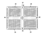
- FIG. 1 is a plan view showing a transistor array according to an embodiment of the present invention.
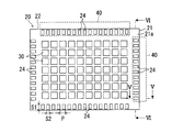
- 2 is an enlarged plan view showing one transistor substrate of the transistor array shown in FIG.
- FIG. 3 is a longitudinal sectional view showing an example of a transistor circuit formed on a transistor substrate.
- FIG. 4 is a longitudinal sectional view for explaining an application example of a transistor circuit.
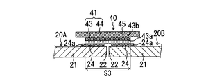
- FIG. 5 is a longitudinal sectional view showing a case where the transistor substrate and the connection member of FIG. 2 are cut in the VV direction.
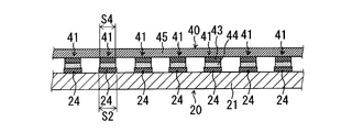
- 6 is a longitudinal sectional view showing a case where the transistor substrate and the connection member of FIG. 2 are cut in the VI-VI direction.
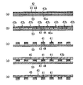
- 7A to 7E are views showing an example of a method for manufacturing a connection member.
- FIG. 1 is a plan view showing a transistor array according to an embodiment of the present invention.
- FIG. 3 is a longitudinal sectional view showing an example of a transistor circuit formed on a transistor substrate.
- FIG. 4 is a longitudinal sectional view for explaining an application
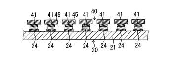
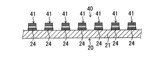
- FIG. 8 is a longitudinal sectional view showing a modification of the connection member.
- FIG. 9 is a longitudinal sectional view showing a modification of the connection member.
- FIG. 10A is a longitudinal sectional view showing a modification of the transistor circuit.
- FIG. 10B is a longitudinal sectional view showing a modification of the connection member.
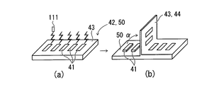
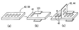
- FIGS. 11A and 11B are diagrams illustrating a manufacturing process of the connection member in the second embodiment.
- 12 (a) to 12 (c) are diagrams illustrating a manufacturing process of a connection member in Example 3.
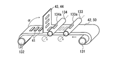
- FIG. FIG. 13 is a diagram for explaining a connection member manufacturing process according to the fourth embodiment.
- FIGS. 1 to 7A to 7E In the drawings attached to the present specification, for the sake of illustration and ease of understanding, the scale, the vertical / horizontal dimension ratio, and the like are appropriately changed and exaggerated from those of the actual ones. Further, in this specification, the terms “substrate”, “base material”, and “film” are not distinguished from each other only based on the difference in names. For example, “substrate” and “base material” are concepts including members that can be called sheets and films. Furthermore, as used in this specification, the shape and geometric conditions and the degree thereof are specified. For example, terms such as “rectangular”, values of length and angle, and the like are not limited to strict meanings. The range of functions that can be expected is interpreted.
- the transistor array 10 includes a plurality of transistor substrates 20 arranged adjacent to each other, and a connection member 40 that electrically connects the two adjacent transistor substrates 20.
- the transistor array 10 is configured by combining four transistor substrates 20 having a rectangular shape. Note that the shape of the transistor substrate 20 and the number of transistor substrates 20 to be combined are not particularly limited as long as the adjacent transistor substrates 20 can be electrically connected appropriately.
- FIG. 2 is an enlarged plan view showing one transistor substrate 20 of the transistor array 10 shown in FIG.
- a connecting member 40 for connecting adjacent transistor substrates 20 is indicated by a dotted line for convenience.
- the transistor substrate 20 is arranged along a base material 21, a plurality of transistor circuits 30 formed on the base material 21, and an outer edge 22 of the base material 21, and is electrically connected to the transistor circuit 30. And a plurality of electrode portions 24 connected to each other, and a wiring formed on the base material 21 and connected to the transistor circuit 30 or the electrode portion 24.
- the plurality of transistor circuits 30 are arranged in a matrix as shown in FIG. Note that in FIG. 1 and FIG. 2, wirings connected to the transistor circuit 30 or the electrode unit 24 are omitted in order to prevent the drawings from becoming complicated.
- FIG. 2 shows an example in which the transistor circuit 30 and the electrode part 24 are both formed on the first surface 21a side of the base material 21.
- the transistor circuit 30 and the electrode unit 24 may be formed on different surfaces.
- the electrode part 24 may be formed on the first surface 21a side of the base material 21, and the transistor circuit 30 may be formed on the second surface side opposite to the first surface 21a. .
- the electrode unit 24 is used to transmit a signal for controlling or driving the transistor circuit 30 or a signal detected by the transistor circuit 30 to a circuit outside the transistor array 10 or an adjacent transistor substrate 20. It is. Note that it is not necessary for all the electrode portions 24 to be electrically connected to the transistor circuit 30, and at least a part of the electrode portions 24 may be connected to the transistor circuit 30. In the example illustrated in FIG. 2, the electrode portions 24 are arranged along each of the four sides included in the rectangular outer edge 22. Further, in two of the four sides, the electrode part 24 is electrically connected to the electrode part 24 of the adjacent transistor substrate 20 via the connection member 40. In addition, although not shown, a substrate or a cable connected to a circuit outside the transistor array 10 may be coupled to the electrode portions 24 arranged along the remaining two sides of the four sides. .
- the dimensions of the electrode portions 24 and the arrangement pitch P of the electrode portions 24 are appropriately set according to the specifications of the transistor substrate 20 and the like.
- the length S1 of the electrode part 24 is in the range of 0.5 mm to 5 mm
- the width S2 of the electrode part 24 is in the range of 0.05 mm to 50 mm.
- the arrangement pitch P of the electrode portions 24 is in the range of 0.1 mm to 100 mm.
- the length S1 of the electrode part 24 is a dimension of the electrode part 24 in a direction orthogonal to the direction in which the sides of the base material 21 on which the electrode parts 24 are arranged are extended, as shown in FIG.
- the width S2 of the electrode part 24 and the arrangement pitch P of the electrode part 24 are the dimension of the electrode part 24 and the arrangement pitch of the electrode part 24 in the direction in which the sides of the base material 21 on which the electrode parts 24 are arranged are extended. .
- the material constituting the electrode part 24 is not particularly limited.
- silver, aluminum, copper, or the like can be used as a material constituting the electrode unit 24.
- the material constituting the base material 21 is not particularly limited.
- the base material 21 may be a flexible substrate having flexibility or a rigid substrate having no flexibility.
- transistor circuit 30 formed on the transistor substrate 20
- the transistor circuit 30 is configured as a pressure sensor circuit for detecting the distribution of pressure applied from the outside
- the transistor array 10 in the present embodiment functions as one member constituting the pressure sensor.
- the transistor circuit 30 includes a gate electrode 31 provided on the first surface 21 a of the substrate 21 and a gate provided on the first surface 21 a of the substrate 21 so as to cover the gate electrode 31.
- a source electrode 33 and a drain electrode 34 provided on the gate insulating film 32 so as to face the insulating film 32 with a certain space therebetween, and a source electrode 33 and a drain electrode 34 so as to be in contact with the source electrode 33 and the drain electrode 34.
- a semiconductor layer 35 provided between and an insulating layer 36 provided so as to cover the source electrode 33, the drain electrode 34, and the semiconductor layer 35.
- a first electrode 37 is provided on the insulating layer 36, and the first electrode 37 is electrically connected to the source electrode 33 or the drain electrode 34 through a through hole 36 a formed in a part of the insulating layer 36. It is connected to the.
- a through hole 36a is formed on the drain electrode 34, and the drain electrode 34 and the first electrode 37 are electrically connected through the through hole 36a.
- the first electrode 37 may be filled in the entire area of the through hole 36a, or may be provided only on the wall surface of the through hole 36a.
- the gate electrode 31 As the material constituting the gate electrode 31, the gate insulating film 32, the source electrode 33, the drain electrode 34, the insulating layer 36, and the first electrode 37, known materials used in transistors are used. For example, the material disclosed in Patent Document 1 described above can be used.
- an inorganic semiconductor material or an organic semiconductor material may be used, but an organic semiconductor material is preferably used.
- an organic semiconductor material a low molecular organic semiconductor material such as pentacene or a high molecular organic semiconductor material such as polypyrrole can be used. More specifically, a low molecular organic semiconductor material or a high molecular organic semiconductor material disclosed in JP2013-21190A can be used.
- the “low molecular organic semiconductor material” means, for example, an organic semiconductor material having a molecular weight of less than 10,000.
- the “polymeric organic semiconductor material” means, for example, an organic semiconductor material having a molecular weight of 10,000 or more.
- a pressure sensitive body 38 is provided on the first electrode 37, and a second electrode 39 is provided on the pressure sensitive body 38.
- the pressure-sensitive body 38 is configured such that the electric resistance value of the pressure-sensitive body 38 in the direction in which the pressure is applied, here in the thickness direction, changes according to the pressure applied to the pressure-sensitive body 38. That is, in the present embodiment, the pressure sensitive body 38 is configured as a so-called pressure sensitive conductor.
- the pressure-sensitive conductor includes, for example, rubber such as silicone rubber and a plurality of conductive particles such as carbon added to the rubber.
- FIG. 3 shows an example in which the transistor type included in the transistor circuit 30 is a so-called bottom gate / bottom contact type.
- the type of transistor included in the transistor circuit 30 is not limited to the bottom gate / bottom contact type.
- a transistor circuit 30 including a top gate / bottom contact type, bottom gate / top contact type, or top gate / top contact type transistor may be used.
- FIG. 4 is a longitudinal sectional view showing a portion of the transistor substrate 20 including a plurality of transistor circuits 30.
- the pressure sensitive body 38 and the second electrode 39 described above may be provided continuously across the plurality of transistor circuits 30. That is, the pressure sensitive body 38 and the second electrode 39 may be used in common in each transistor circuit 30.
- An overcoat layer 26 having an insulating property may be provided on the second electrode 39.
- the pressure sensitive body 38 when pressure is applied to the transistor substrate 20 via a pen 60 or the like in a part of the transistor substrate 20, the pressure sensitive body 38 is compressed in the thickness direction in the applied portion. As a result, the particles in the pressure sensitive body 38 come into contact with each other in the thickness direction, and the electric resistance value of the pressure sensitive body 38 in the thickness direction becomes low. For this reason, in the transistor circuit 30 including the pressure-sensitive body 38 to which pressure is applied, the current flowing through the source electrode 33 and the drain electrode 34 increases. Therefore, the distribution of the pressure applied to the transistor substrate 20 can be calculated by detecting the value of the current flowing through each transistor circuit 30.
- the transistor circuit 30 when the transistor circuit 30 is configured as a pressure sensor circuit, various pressures are applied to each transistor substrate 20 of the transistor array 10 during a test before shipment or during use after shipment.
- the pressure sensor circuit when the pressure sensor circuit is for measuring the pressure applied from the foot during walking as disclosed in JP2013-113780A, the pressure applied to the transistor substrate 20 is extremely large. It becomes. Therefore, it is preferable that the connection member 40 that connects the plurality of transistor substrates 20 is configured to be able to individually replace the transistor substrate 20 in which a defect or defect has occurred.
- the connection member 40 in the present embodiment will be described in detail with reference to FIGS. 5 and 6.
- FIG. 5 is a longitudinal sectional view showing a case where the transistor substrate 20 and the connection member 40 of FIG. 2 are cut in the VV direction, that is, in a direction crossing the outer edge 22 of the base material 21.
- 6 is a longitudinal sectional view showing a case where the transistor substrate 20 and the connecting member 40 of FIG. 2 are cut in the VI-VI direction, that is, in the direction along the outer edge 22 of the base material 21.
- one of the two adjacent transistor substrates 20 is represented by reference numeral 20A.
- the other transistor substrate 20 adjacent to one transistor substrate 20A is represented by reference numeral 20B.
- connection member 40 includes a plurality of electrode portions 24 that electrically connect the plurality of electrode portions 24 of the one transistor substrate 20A and the plurality of electrode portions 24 of the other transistor substrate 20B, respectively.
- the conductive member 41 and a support member 45 extending across the plurality of conductive members 41 so as to support the conductive member 41 are included.
- One conductive member 41 is connected to one electrode portion 24 of one transistor substrate 20A and one electrode portion 24 of the other transistor substrate 20B so as to be peelable and reattachable.
- the conductive member 41 in the present embodiment includes a plurality of conductive layers.
- the conductive member 41 includes a conductive layer 43 including a first surface 43 a and a second surface 43 b located on the opposite side of the first surface 43 a, and a conductive layer 43 on the first surface 43 a side.
- a conductive adhesive layer 44 provided.
- FIG. 5 by disposing the connecting member 40 so that the conductive adhesive layer 44 is in contact with the electrode portion 24 of one transistor substrate 20A and the electrode portion 24 of the other transistor substrate 20B, one transistor substrate 20A is disposed. Electrical connection between the first electrode portion 24 and the second electrode portion 24 of the transistor substrate 20B is ensured.
- the size of the conductive member 41 is not particularly limited.
- the length S ⁇ b> 3 of the conductive member 41 is set so that the conductive member 41 does not cover the end 24 a of the electrode portion 24, but the present invention is not limited to this, and the conductive member 41 is not limited thereto.
- the length S3 of the conductive member 41 may be set so as to cover the end 24a of the electrode part 24.
- 6 shows an example in which the width S4 of the conductive member 41 is smaller than the width S2 of the electrode portion 24.
- the present invention is not limited to this, and the conductive member 41, more specifically, the conductive adhesive layer, is shown.
- the width S4 of 44 may be larger than the width S2 of the electrode portion 24.
- the electrode part 24 of one transistor substrate 20A and the electrode part 24 of the other transistor substrate 20B are Even if it is shifted in the width direction, the electrode member 24 to be connected can be entirely covered in the width direction by the conductive member 41, so that a good electrical connection can be ensured.
- the transistor substrates 20A and 20B are organic thin film transistor substrates using organic semiconductor materials, that is, OTFT substrates, due to their flexibility, the electrode portions 24 to be connected may be easily displaced. . In such a case, the connection member 40 in which the width S4 of the conductive member 41 is larger than the width S2 of the electrode part 24 can be used particularly beneficially.
- the conductive layer 43 is a layer configured to have higher conductivity than the conductive adhesive layer 44.
- a metal material such as silver, copper, or aluminum can be used.
- the conductive layer 43 may be configured using an oxide conductor such as indium tin oxide or indium zinc oxide.
- the conductive layer 43 may be configured by combining a plurality of conductive layers.
- the thickness of the conductive layer 43 is in the range of 5 ⁇ m to 200 ⁇ m, for example.
- the conductive adhesive layer 44 is a layer configured to have adhesiveness and conductivity.
- the conductive adhesive layer 44 includes an adhesive and a plurality of conductive particles added to the adhesive.
- the conductive adhesive layer 44 may be formed by applying a paste-like material containing an adhesive and conductive particles to the conductive layer 43, or a tape-like member or film containing the adhesive and conductive particles. It may be formed as a shaped member.
- an adhesive and electroconductive particle the material used in a general electroconductive tape can be employ
- a silicone resin or an acrylic resin can be employed as the adhesive.
- the conductive particles may contain at least one of metal and carbon.
- the metal contained in the conductive particles may contain at least one of nickel, gold, silver, copper, or aluminum.
- carbon contained in electroconductive particle what has electroconductivity can be used among the substances comprised, such as graphite and carbon black, for example.
- the conductive particles may contain a plating powder.
- the plating powder is particles obtained by forming a metal layer on the surface of the base powder by electroless plating or the like.
- nickel, gold, silver, copper, aluminum, or the like can be used as a metal contained in the metal layer of the plating powder.
- the conductive adhesive layer 44 is formed not only after the connection member 40 is connected to the electrode part 24 of the transistor substrate 20 but also before the connection member 40 is connected to the electrode part 24 in the thickness direction of the conductive adhesive layer 44. It is comprised so that it may have electroconductivity. For example, the plurality of conductive particles of the conductive adhesive layer 44 are in contact with each other in the thickness direction so that the conductivity in the thickness direction of the conductive adhesive layer 44 is ensured. This means that when the connection member 40 is attached to the electrode portion 24 of the transistor substrate 20, a thermocompression bonding step as performed in conventional tiling is not necessary.
- the dimension and arrangement pitch of the electroconductive member 41 of the connection member 40 are not restrict
- the width S4 of the conductive member 41 can be set to a value substantially equal to the width S2 of the electrode portion 24, that is, within a range of 0.05 mm to 50 mm.
- the thermocompression bonding process is unnecessary, the attaching work and the removing work of the connecting member 40 are facilitated as compared with the conventional case. Therefore, when a defect or defect occurs in a part of the transistor substrates 20, the transistor array 10 can be easily repaired by replacing only part of the transistor substrates 20.
- the adhesive strength of the conductive adhesive layer 44 in the connection member 40 can be set as appropriate depending on the weight of the transistor substrate 20 to be connected, the usage environment, and the like. For example, when measured in a test based on JIS Z 0237, The value may be about 25 mm.
- the present inventor can connect the transistor substrate 20 in a state where the connection member 40 is stable when the adhesive force is in the above range, can remove the connection member 40 relatively easily, and can remove the electrode portion 24 at the time of removal. It has been found that is not impaired.
- the conductive adhesive layers 44 of the plurality of conductive members 41 are physically separated from each other. For this reason, even if the conductive adhesive layer 44 has conductivity not only in the thickness direction but also in the plane direction, the two adjacent electrode portions 24 of the transistor substrate 20 do not conduct. Therefore, the conductive adhesive layer 44 may be configured to have conductivity in both the thickness direction and the surface direction. That is, the plurality of conductive particles of the conductive adhesive layer 44 may be in contact with each other also in the plane direction in addition to the thickness direction.
- the “plane direction” is a direction along the first surface 43 a of the conductive layer 43.
- ⁇ 2 is within the range of 0.5 ⁇ ⁇ 1 to 1.0 ⁇ ⁇ 1, for example. It has become.
- the conductive member 41 is provided on the second surface 43b side of the conductive layer 43 in addition to the conductive layer 43 and the conductive adhesive layer 44 provided on the first surface 43a side of the conductive layer 43.
- the conductive adhesive layer 44 provided may be further included. Thereby, the adhesive force between the conductive member 41 and the support member 45 can be increased, and thereby the reliability of the connection member 40 can be increased.
- the support member 45 is a member provided on the second surface 43 b side of the conductive layer 43 so as to support the plurality of conductive members 41 while having insulating properties.
- the support member 45 is configured to have flexibility.
- a resin such as polyimide, polyethylene naphthalate, or polyethylene terephthalate can be used.
- the thickness of the support member 45 is preferably set in the range of 5 ⁇ m to 200 ⁇ m.
- connection member 40 Manufacturing method of connecting member
- a laminate including a separator 50 and a conductive laminate 42 as a conductive material layer provided on the separator 50 is prepared.
- the conductive laminate 42 includes a conductive layer 43 including a first surface 43a and a second surface 43b located on the opposite side of the first surface 43a, and a conductive adhesive layer provided on the first surface 43a side of the conductive layer 43. 44.
- the separator 50 is a member that supports the conductive laminate 42 during the manufacturing process of the connection member 40 and is peeled from the connection member 40 including the conductive laminate 42 after the manufacturing process of the connection member 40 is completed. is there.
- the separator 50 is configured so that the conductive adhesive layer 44 can be easily peeled off.
- the adhesive force of the conductive adhesive layer 44 to the separator 50 is smaller than the adhesive force of the conductive adhesive layer 44 to the conductive layer 43.
- a conductive tape having a thickness of several tens of ⁇ m including a conductive layer 43 made of copper or aluminum and a conductive adhesive layer 44 is used.
- the separator 50 what contains resin, glass, etc. is used, for example.
- the shape and thickness of the separator 50 are not specifically limited.
- the separator 50 may be a film having flexibility that can be bent or curved. Alternatively, it may be a plate having a certain degree of rigidity.
- a cutting process for cutting the conductive laminate 42 on the separator 50 is performed. Specifically, first, as shown in FIG. 7B, cuts 42 a are formed at each position of the conductive laminate 42 from the second surface 43 b of the conductive layer 43 to the surface of the separator 50. At this time, the cuts 42a are formed so that a plurality of portions represented by reference numeral 42b in FIG. 7B in the conductive laminate 42 are at least partially connected to each other in the depth direction of the paper surface. Thereafter, by separating the portions 42b connected to each other from the separator 50, as shown in FIG. 7C, each of the conductive layers 42 includes the above-described conductive laminate 42 and is physically separated from each other. The member 41 can be formed on the separator 50.
- the support member 45 is attached to each conductive member 41 from the second surface 43 b side of the conductive layer 43.
- an adhesive layer or the like for attaching the conductive member 41 to the support member 45 may be provided on the surface of the support member 45 on the conductive member 41 side.
- the separator 50 is peeled off from each conductive member 41.
- a connection member 40 including a support member 45 and a plurality of conductive members 41 provided on the support member 45 can be obtained.
- the conductive member 41 of the connection member 40 has the conductive adhesive layer 44.
- the conductive adhesive layer 44 is formed not only after the connection member 40 is connected to the electrode part 24 of the transistor substrate 20 but also before the connection member 40 is connected to the electrode part 24 in the thickness direction of the conductive adhesive layer 44. It is comprised so that it may have electroconductivity. For this reason, the connection member 40 can be attached to the electrode part 24 of the transistor substrate 20 without performing a thermocompression bonding process. Therefore, it is possible to suppress changes in the hardness and adhesive strength of the conductive member 41 before and after the connection member 40 is attached to the electrode portion 24 of the transistor substrate 20.
- connection member 40 once attached to the electrode portion 24 of the transistor substrate 20 can be easily removed as necessary. Accordingly, the transistor array 10 can be repaired by exchanging only a part of the transistor substrates 20 in which defects or defects have occurred. For this reason, the man-hour and cost which are required for repair of the transistor array 10 can be reduced.
- the conductive member 41 includes the conductive adhesive layer 44 and the conductive layer 43.
- the conductive adhesive layer 44 includes an adhesive, so that the conductivity can be reduced with respect to a material made entirely of a conductive material, but the conductive layer 43 provided in contact with the conductive adhesive layer 44.
- the conductivity of the entire conductive member 41 can be improved. Thereby, the favorable electrical connection between the mutually different electrode parts 24 connected by the connection member 40 can be ensured, and the applicable range can be expanded.
- the transistor array 10 tiled by the connection member 40 functions as one member constituting the pressure sensor.
- the pressure applied to the transistor substrate 20 when receiving pressure from the outside may be extremely large, and there is a high possibility that problems and defects are likely to occur.
- the semiconductor layer 35 of the transistor circuit 30 is preferably an organic thin film transistor circuit made of an organic semiconductor material. In this case, the durability can be improved by stabilizing the mechanical strength of the semiconductor layer 35.
- FIG. 10A shows a transistor circuit 30 including a top-gate / bottom-contact transistor as an example of a modification of the transistor circuit 30 in this embodiment.
- the transistor circuit 30 according to this modification includes a source electrode 33 and a drain electrode 34 provided on the base material 21 so as to face each other with a certain interval, and a source electrode 33 so as to be in contact with the source electrode 33 and the drain electrode 34.
- a transistor including A first electrode 37 is provided on the insulating layer 36, and the first electrode 37 is electrically connected to the source electrode 33 through a through hole 36 a formed in a part of the insulating layer 36.
- a bottom-gate transistor can be easily manufactured by using printing or the like, so that production efficiency can be improved.
- a top-gate transistor generally can ensure high semiconductor characteristics, so that power consumption can be reduced and the quality of an embedded device can be improved.
- connection member 40 may include a plurality of conductive members 41 and a plurality of support members 45 provided on the respective conductive members 41. That is, the plurality of support members 45 may be physically separated from each other according to the corresponding conductive member 41.
- connection member 40 may include a plurality of support members 45 configured to spread over a small number of conductive members 41 such as two or three. Thus, by setting the extending range of the support member 45 to be smaller, the transistor array 10 can be repaired for each smaller section.
- the example in which the conductive laminate 42 is separated into a plurality of island-shaped portions by performing the cutting step of cutting the conductive laminate 42 on the separator 50 has been described.
- the method used is not limited to cutting.
- the conductive laminate 42 may be separated into a plurality of portions by using an etching method.
- connection member 40 includes the support member 45 provided on the second surface 43b side of the conductive layer 43 of the conductive member 41 .
- the present invention is not limited to this.
- the connection member 40 only needs to include at least a conductive member 41 coupled to the electrode portion 24 of the transistor substrate 20. That is, the support member 45 may not be provided on the connection member 40.
- Such a connection member 40 is obtained by attaching a plurality of conductive members 41 formed on the separator 50 to the electrode part 24 of the transistor substrate 20 one by one as shown in FIG. Also good. Alternatively, it may be obtained by attaching the connecting member 40 having the conductive member 41 and the support member 45 to the electrode portion 24 of the transistor substrate 20 and then peeling the support member 45 from the conductive member 41.
- FIG. 10B shows As shown, the conductive member 41 may have only the conductive adhesive layer 44.
- a connecting member 40 shown in FIG. 10B includes a conductive member 41 having only a conductive adhesive layer 44 and a support member 45.
- the transistor array 10 can be thinned by suppressing the thickness of the connection member 40.
- the connection member 40 shown to FIG. 10B has the supporting member 45, the supporting member 45 does not need to be provided.
- the surface of the conductive adhesive layer 44 opposite to the surface in contact with the electrode portion 24 is treated so as not to have adhesiveness.
- another film-like member may be provided on the surface of the conductive adhesive layer 44 opposite to the surface in contact with the electrode portion 24.
- the pressure-sensitive body 38 is a so-called pressure-sensitive conductor in which the electric resistance of the pressure-sensitive body 38 changes according to the pressure applied to the pressure-sensitive body 38.
- An example is shown.
- the specific configuration of the pressure sensitive body 38 is not particularly limited.
- the pressure sensitive body 38 may be configured such that the capacitance of the pressure sensitive body 38 changes in accordance with the pressure applied to the pressure sensitive body 38.
- the transistor circuit 30 is configured as a pressure sensor circuit for detecting the distribution of pressure applied from the outside.
- the physical quantity detected by the transistor circuit 30 is not limited to pressure, and may be a physical quantity such as light intensity, electromagnetic field intensity, and temperature.
- the specific application of the transistor circuit 30 is not limited to the sensor circuit.
- the transistor circuit 30 may be configured as a drive circuit for individually driving a plurality of elements of the display device. According to the present embodiment, it is possible to provide the transistor array 10 that can be easily partially repaired regardless of the application of the transistor circuit 30.
- the composite wiring board composed of a plurality of wiring boards electrically connected via the connection member 40 is electrically connected via the connection member 40, and the transistor circuit 30 is connected.
- the example which is the transistor array 10 comprised by the several transistor substrate 20 which has is shown. That is, an example in which the plurality of wiring boards electrically connected via the connection member 40 is the transistor substrate 20 has been shown.
- the wiring boards that are electrically connected via the connection member 40 are not limited to the transistor substrates 20.
- the connection member 40 described above may be used when a plurality of flexible boards on which wiring and electrode portions are formed are electrically connected to each other. Examples of the flexible substrate mentioned here include a flexible printed circuit board, so-called FPC, and the like.
- connection member 40 when the adjacent transistor substrate 20 and the flexible substrate are electrically connected to each other, the connection member 40 described above may be used. Therefore, the composite wiring board constituted by a plurality of wiring boards electrically connected via the connection member 40 is configured by electrically connecting the plurality of transistor substrates 20 to each other using the connection member 40.
- the connection member 40 is used to electrically connect a plurality of flexible substrates to each other, or the connection member 40 is used to connect the transistor substrate 20 and the flexible substrate to each other. What is comprised by electrically connecting is also included.
- Examples 1 to 4 of the present invention will be described.
- the transistor array 10 is manufactured by tiling a plurality of organic thin film transistor substrates, that is, OTFT substrates, manufactured as the transistor substrate 20 with the connection member 40 manufactured separately will be described. .
- Example 1 in the production of the transistor substrate 20 which is an organic thin film transistor substrate, first, a negative photosensitive resin was spin-coated on a base material 21 made of a PEN (polyethylene naphthalate) film having a thickness of 0.1 mm. This was applied, and then baked at 150 ° C. for 30 minutes to form a negative photosensitive resin planarizing layer. Next, an Al sputtered film having a thickness of 200 nm was formed by sputtering aluminum on the entire surface of the flat layer of the negative photosensitive resin on the base material 21. Then, a positive photoresist was applied on the Al sputtered film by spin coating to form a resist layer.
- PEN polyethylene naphthalate
- the resist layer was patterned by performing exposure and development using a photomask on the resist layer. Then, in the etching process, after etching the Al sputtered film exposed from the portion of the patterned resist layer where the resist is not formed, the resist layer was removed. Thereby, the gate electrode 31 and the data wiring connected thereto were formed on the base material 21.
- an ultraviolet photosensitive acrylic resin was applied onto the gate electrode 31 by spin coating, thereby forming a gate insulating layer covering the gate electrode 31.
- the gate insulating layer was patterned by performing exposure using a photomask and alkali development on the gate insulating layer.
- the gate insulating film 32 having a thickness of 1 ⁇ m was formed by heat curing at 150 ° C. in an oven for 30 minutes.
- a silver sputtering film having a thickness of 40 nm was formed by sputtering silver on the gate insulating film 32.
- a positive photoresist was applied on the sputtered silver film by spin coating to form a resist layer.
- the resist layer was patterned by performing exposure and development using a photomask on the resist layer.
- the resist layer was removed.
- the source electrode 33, the drain electrode 34, and the data wiring connected thereto were formed on the gate insulating film 32.
- a xylene solution of an organic semiconductor in which a thiophone-based polymer is dissolved in xylene at a solid content concentration of 1 wt% is prepared, and this xylene solution is applied to the surface of the substrate on which the source electrode 33, the drain electrode 34, and the data wiring are formed.
- the organic semiconductor layer with a film thickness of 50 nm was formed in the whole base-material surface by apply
- a positive resist was applied on the organic semiconductor layer by spin coating to form a resist layer. Then, the resist layer was patterned by performing exposure using a photomask and alkali development on the resist layer.
- the organic semiconductor layer other than the portion covered with the resist layer on the organic semiconductor layer is etched and removed.
- the organic semiconductor layer was patterned, and then the resist layer was removed. Thereby, a semiconductor layer 35 made of an organic semiconductor material was formed.
- a passivation layer was formed by applying an ultraviolet photosensitive acrylic resin on the semiconductor layer 35 by spin coating. Then, the passivation layer was patterned so that a through-hole 36a exposing the drain electrode 34 was formed by performing exposure using a photomask and alkali development on the passivation layer. Next, a cured passivation layer was formed by heat curing at 150 ° C. for 30 minutes in an oven. Thereafter, an electrode or the like electrically connected to the drain electrode 34 was formed. In addition, an electrode portion 24 arranged along the outer edge 22 of the substrate 21 was provided. A part of the electrode part 24 is connected to the gate electrode 31, the source electrode 33, or the drain electrode 34 through a data wiring formed on the substrate 21 by processes such as patterning and etching. Thus, a transistor substrate 20 having a plurality of transistor circuits 30 according to Example 1 was produced.
- a conductive adhesive tape was prepared as a laminate including the separator 50 and the conductive laminate 42 provided on the separator 50.
- the conductive adhesive tape has a thickness of about 80 ⁇ m, and the conductive laminate 42 including the conductive layer 43 and the conductive adhesive layer 44 has a thickness of about 50 ⁇ m.
- the conductive layer 43 is made of aluminum.
- the conductive adhesive tape is cut with a cutting machine so that a plurality of rectangular cuts of 2 mm ⁇ 5 mm are formed at intervals of 2 mm in the conductive layer 43 and the conductive adhesive layer 44 in the conductive adhesive tape. Cutting was performed from the 43 side toward the separator 50 side. Then, the conductive layer 43 and the conductive adhesive layer 44 that are integrally connected to the outside of the above-mentioned notches are peeled from the separator 50, whereby the separator 50 is arranged in an island-like pattern at intervals of 2 mm. A plurality of 5 mm rectangular conductive members 41 were formed.
- connection member 40 was produced.
- the two transistor substrates 20 manufactured as described above were prepared, and the two transistor substrates 20 were arranged in a line so that the electrode portions 24 to be connected to each transistor substrate 20 face each other.
- the transistor array 10 by which the two transistor substrates 20 were tiled was produced by attaching the above-mentioned connection member 40 to each electrode part 24 so that each electrode part 24 might be straddled.
- the electrical resistance value between the one substrate 20 and the other substrate 20 is measured to be 10 ⁇ or less via the connection member 40, and the substrate It was confirmed that 20 was well connected electrically. Further, when the connecting member 40 was peeled off and again attached to the electrode portion 24 of each transistor substrate 20 and tiled, the two transistor substrates 20 were well connected. Moreover, the electrical resistance value at this time was the same value as the state before peeling. Thus, it was confirmed that the transistor substrate 20 can be partially repaired in the transistor array 10 in which the plurality of transistor substrates 20 are tiled.
- Example 2 Next, Example 2 will be described.
- the transistor substrate 20 was produced in the same procedure as in Example 1.
- the manufacturing procedure of the connection member 40 is different from that of the first embodiment. Below, the preparation procedure of the connection member 40 which concerns on Example 2 is explained in full detail.
- Example 2 when producing the connection member 40, first, a conductive adhesive tape was prepared as a laminate including the separator 50 and the conductive laminate 42 provided on the separator 50.
- the conductive adhesive tape has a thickness of about 50 ⁇ m, and the conductive laminate 42 including the conductive layer 43 and the conductive adhesive layer 44 has a thickness of about 30 ⁇ m.
- the conductive layer 43 is made of copper.
- the conductive layer 43 and the conductive adhesive layer 44 in the conductive adhesive tape are conductive so that a plurality of 2 mm ⁇ 5 mm rectangular cuts are formed at intervals of 2 mm.
- the adhesive tape was cut from the conductive layer 43 side toward the separator 50 side by irradiation with a CO 2 laser having a wavelength of 10.6 ⁇ m from the CO 2 laser oscillation device 111.
- the conductive layer 43 and the conductive adhesive layer 44 that are integrally connected outside the above-mentioned notch are separated from the separator 50 in the direction of the arrow ⁇ , thereby separating the separator.
- a plurality of 2 mm ⁇ 5 mm rectangular conductive members 41 that are patterned in an island shape and arranged at intervals of 2 mm are formed on 50.
- the polyimide tape as the support member 45 is adhered to the conductive portion 43 of the conductive member 41 by adhesion, and then the plurality of conductive members 41 are peeled off from the separator 50 to thereby support the plurality of conductive members 41 as the support members. 45.
- the connection member 40 according to Example 2 was produced.
- the transistor array 10 including the two transistor substrates 20 that are tiled by the connection member 40 according to the second embodiment may be well electrically connected as in the first embodiment. confirmed. Further, even when the connecting member 40 is peeled off and again attached to the electrode portion 24 of each transistor substrate 20 and tiled, the two transistor substrates 20 are well connected and the electric resistance value at this time was the same value as in the state before peeling.
- Example 3 Next, Example 3 will be described. Also in Example 3, the transistor substrate 20 was produced in the same procedure as in Example 1. On the other hand, the manufacturing procedure of the connection member 40 is different from those in the first and second embodiments. A procedure for producing the connection member 40 according to Example 3 will be described in detail below.
- Example 3 when manufacturing the connection member 40, first, as shown in FIG. 12A, as a laminate including the separator 50 and the conductive laminate 42 provided on the separator 50, a conductive material is used. Adhesive tape was prepared. The conductive adhesive tape has a thickness of about 50 ⁇ m, and the conductive laminate 42 including the conductive layer 43 and the conductive adhesive layer 44 has a thickness of about 30 ⁇ m. The conductive layer 43 is made of copper.
- the conductive layer 43 and the conductive adhesive layer 44 in the above-mentioned conductive adhesive tape are electrically conductive so that a plurality of rectangular cuts of 2 mm ⁇ 5 mm are formed at intervals of 2 mm.
- the adhesive tape was cut from the conductive layer 43 side toward the separator 50 side by continuous punching of the metal mold 121.
- the mold 121 is formed with a frame-shaped punching portion for forming a rectangular cut of 2 mm ⁇ 5 mm.
- the conductive layer 43 and the conductive adhesive layer 44 that are integrally connected to the outside of the notch are peeled from the separator 50 in the direction of the arrow ⁇ , thereby separating the separator.
- a plurality of 2 mm ⁇ 5 mm rectangular conductive members 41 that are patterned in an island shape and arranged at intervals of 2 mm are formed on 50.
- the polyimide tape as the support member 45 is adhered to the conductive portion 43 of the conductive member 41 by adhesion, and then the plurality of conductive members 41 are peeled off from the separator 50 to thereby support the plurality of conductive members 41 as the support members. 45.
- the connection member 40 according to Example 3 was produced.
- the transistor array 10 including the two transistor substrates 20 tiled by the connection member 40 according to the third embodiment may be well electrically connected as in the first embodiment. confirmed. Further, even when the connecting member 40 is peeled off and again attached to the electrode portion 24 of each transistor substrate 20 and tiled, the two transistor substrates 20 are well connected and the electric resistance value at this time was the same value as in the state before peeling.
- Example 4 Next, Example 4 will be described. Also in Example 4, the transistor substrate 20 was produced in the same procedure as in Example 1. On the other hand, the manufacturing procedure of the connecting member 40 is different from those in the first to third embodiments. The procedure for producing the connection member 40 according to Example 4 will be described in detail below.
- Example 4 when the connection member 40 was produced, first, a conductive adhesive tape was prepared as a laminate including the separator 50 and the conductive laminate 42 provided on the separator 50.
- the conductive adhesive tape has a thickness of about 50 ⁇ m, and the conductive laminate 42 including the conductive layer 43 and the conductive adhesive layer 44 has a thickness of about 30 ⁇ m.
- the conductive layer 43 is made of copper.
- the conductive adhesive tape was wound around the supply roller 131 shown in FIG. 13 with the conductive layer 43 positioned outside. Thereafter, the conductive adhesive tape is unwound from the supply roller 131 and hung around the transport roller 132 disposed away from the supply roller 132, so that the conductive adhesive tape is placed between the supply roller 131 and the transport roller 132. It arranged in the state which straddles. As a result, the conductive adhesive tape was placed in a state where it was fed from the supply roller 131 and conveyed to the conveying roller 132 side.
- a first die roll 133 formed by projecting a frame-shaped punching portion 133a for forming a rectangular cut of 2 mm ⁇ 5 mm on the conductive adhesive tape is formed on the outer surface.
- the punching portion 133a is rotated, It arrange
- a second die roll 134 having a frame-shaped punching portion 134a formed on the outer surface for forming a rectangular cut of 2 mm ⁇ 5 mm on the conductive adhesive tape is formed by rotating the punching portion 134a. It arrange
- die roll 133 is a member for forming a notch in the conductive layer 43, and is arrange
- the second mold roll 134 is a member for forming a cut in the conductive adhesive layer 44, and is disposed downstream of the first mold roll 133 in the transport direction of the conductive adhesive tape.
- the conductive layer 43 and the conductive adhesive layer 44 that are integrally connected to the outside of the notch are peeled from the separator 50 in the direction of the arrow ⁇ , so that the separator 50 is placed on the separator 50.
- a plurality of 2 mm ⁇ 5 mm rectangular conductive members 41 that were patterned in an island shape at intervals of 2 mm were formed.
- the separator 50 having a plurality of conductive members 41 formed thereon was removed from the supply roller 131 and the transport roller 132, and the polyimide tape as the support member 45 was adhered to the conductive portion 43 of the conductive member 41 by adhesion.
- the plurality of conductive members 41 were transferred to the support member 45 by peeling the plurality of conductive members 41 from the separator 50.
- the connection member 40 according to Example 4 was produced.
- the transistor array 10 including the two transistor substrates 20 tiled by the connection member 40 according to the fourth embodiment as described above may be well electrically connected as in the first embodiment. confirmed. Further, even when the connecting member 40 is peeled off and again attached to the electrode portion 24 of each transistor substrate 20 and tiled, the two transistor substrates 20 are well connected and the electric resistance value at this time was the same value as in the state before peeling.
Landscapes
- Engineering & Computer Science (AREA)
- Microelectronics & Electronic Packaging (AREA)
- Thin Film Transistor (AREA)
Abstract
【課題】部分的な修復を容易に実施することができる複合配線基板を提供する。 【解決手段】複合配線基板は、互いに隣接するよう並べられた複数の配線基板と、隣接する2つの配線基板を電気的に接続する接続部材と、を備えている。接続部材は、一方の配線基板の複数の電極部と、他方の配線基板の複数の電極部と、をそれぞれ電気的に接続する複数の導電性部材を含んでいる。導電性部材は、粘着剤と、粘着剤に添加された複数の導電性粒子と、を含む導電性粘着層を有している。導電性部材は、導電性粘着層が一方の配線基板の電極部および他方の配線基板の電極部に接するように配置されている。導電性粘着層は、厚み方向および面方向のいずれにおいても導電性を有している。
Description
本発明は、接続部材を介して接続された複数の配線基板を備える複合配線基板に関する。また本発明は、複数の配線基板を電気的に接続するための接続部材およびその製造方法に関する。さらに本発明は、複合配線基板を備える圧力センサに関する。
ディスプレイ装置やセンサ装置などの様々な分野において、半導体層を含むトランジスタを有するトランジスタ回路が広く利用されている。例えばトランジスタ回路は、有機EL(Organic Electroluminescence)ディスプレイ装置の複数の発光素子を個々に駆動するための駆動回路としてや、圧力センサ装置の複数の位置におけるセンサ信号を各々検出するためのセンサ回路として利用されている。トランジスタ回路は一般に、基材と、基材上に形成された複数のトランジスタ回路と、トランジスタ回路に接続された配線と、を備えるトランジスタ基板の形態で提供される。
従来、トランジスタに用いられる半導体材料としては、シリコン、ガリウム砒素やインジウムガリウム砒素などの無機半導体材料が用いられてきた。一方、近年は、有機半導体材料を用いたトランジスタに関する研究も盛んにおこなわれている。有機半導体材料は一般に、無機半導体材料に比べて低い温度で基板上に形成され得る。このため、有機半導体材料を用いた回路や、回路に接続される配線が形成された基板として、フレキシブルなプラスチック基板などを利用することができる。このことにより、機械的衝撃に対する安定性を有し、かつ軽量な半導体素子を提供することが可能となる。また、印刷法等の塗布プロセスを用いて有機半導体材料を基板上に形成することができるので、無機半導体材料が用いられる場合に比べて、多数の有機トランジスタを基板上に効率的に形成することが可能となる。このため、半導体素子の製造コストを低くすることができる可能性がある。これらのことから、有機半導体材料は、有機ELや電子ペーパーなどの駆動回路、または電子タグなどに応用されることが期待されている。なお以下の説明において、配線が形成された基板のことを配線基板とも称する。トランジスタ回路および配線が形成されたトランジスタ基板や、配線が形成されたフレキシブル基板などは、配線基板の例である。
ところで、欠陥が無い、または欠陥が極めて少ないトランジスタ基板を製造するためには、圧力や清浄度が精密に調整された環境が必要になる。従って、基材の面積を拡大することによってトランジスタ基板の大型化を実現することは容易ではない。このような課題を考慮し、例えば特許文献1においては、複数のトランジスタ基板を、それらが互いに隣接するように並べることにより、多数のトランジスタ回路を備えた大面積のトランジスタアレイを構成することが提案されている。この場合、隣接する2つのトランジスタ基板は、トランジスタ基板上に形成された電極部に、フレキシブル基板を用いて構成された接続部材を連結することによって、電気的に接続される。このように複数のトランジスタ基板を互いに連結することは、タイリングとも称される。
上述のように複数のトランジスタ基板を組み合わせて大面積のトランジスタアレイを作製することにより、個々のトランジスタ基板の面積を比較的に小さくすることができる。このため、個々のトランジスタ基板の製造工程において欠陥が生じることを抑制することができる。
上述のトランジスタアレイなど、接続部材を介して電気的に接続された複数の配線基板によって構成される複合配線基板においては、出荷前の試験時や、出荷後の使用時に、複合配線基板を構成する複数の配線基板のうちの一部、例えば1枚の配線基板についてのみ不具合や欠陥が生じるまたは判明することがある。この場合、その他の配線基板は正常な状態にあるので、1枚の配線基板のみを交換することによってトランジスタアレイなどの複合配線基板を修復することが好ましい。
一方、従来のタイリングにおいては、特許文献1にも記載されているように、フレキシブル基板に設けられた異方性導電材料を含む接続部材が利用される。この場合、はじめに、接続部材を配線基板の電極部の上に載置し、次に、接続部材を配線基板へ熱圧着することにより、接続部材と配線基板とが電気的に接続される。このように従来は熱圧着によって接続部材と配線基板とが連結されているため、接続部材をいったん配線基板に取り付けた後に接続部材を配線基板から取り外すことは困難である。このため、一部の配線基板にのみ不具合や欠陥が生じた場合であっても、一部の配線基板のみを交換してトランジスタアレイを修復することは容易ではない。
また、熱圧着工程を適切に実施するためには、ある程度の面積にわたって接続部材を配線基板に対して平行に押圧することが求められる。すなわち接続部材の面積は、適切な押圧という観点で定められる最小値以上になっている必要がある。一方、熱圧着工程においては、接続部材を加熱することによって、異方性導電材料に含まれる導電性粒子を少なくとも部分的に溶融させることが必要になる。一方、広域にわたって均一に接続部材に熱を加えることは容易ではない。従って、接続部材の面積は、適切な加熱という観点で定められる最大値以下になっている必要がある。このように接続部材が異方性導電材料を含む場合、押圧や加熱の観点から接続部材の面積が制約されることになる。このような制約も、トランジスタアレイの部分的な修復を妨げる要因となり得る。
本発明は、このような点を考慮してなされたものであり、部分的な修復を容易に実施することができる複合配線基板およびこれを備える圧力センサを提供することを目的とする。また本発明は、複数の配線基板を電気的に接続するための接続部材およびその製造方法を提供することを目的とする。
本発明の一実施の形態は、互いに隣接するよう並べられた複数の配線基板と、隣接する2つの前記配線基板を電気的に接続する接続部材と、を備え、前記配線基板は、基材と、前記基材の外縁に沿って並べられた複数の電極部と、前記電極部に接続された配線と、を有し、前記接続部材は、一方の前記配線基板の複数の前記電極部と、一方の前記配線基板に隣接する他方の前記配線基板の複数の前記電極部と、をそれぞれ電気的に接続する複数の導電性部材を含み、前記導電性部材は、粘着剤と、前記粘着剤に添加された複数の導電性粒子と、を含む導電性粘着層を有し、前記導電性部材は、前記導電性粘着層が一方の前記配線基板の前記電極部および他方の前記配線基板の前記電極部に接するように配置されており、前記導電性粘着層は、厚み方向および面方向のいずれにおいても導電性を有している、複合配線基板、である。
前記導電性部材は、第1面および前記第1面の反対側に位置する第2面を含む導電層をさらに有し、前記導電性粘着層は、前記導電層の前記第1面側に設けられていてもよい。
前記接続部材は、前記導電性部材の前記導電層の前記第2面側に設けられ、絶縁性を有する支持部材をさらに含んでいてもよい。
前記支持部材は、複数の前記導電性部材に跨って広がっていてもよい。
前記導電性粘着層の前記導電性粒子は、金属または炭素の少なくとも一方を含んでいてもよい。
前記導線性粒子に含まれる前記金属は、ニッケル、金、銀、銅またはアルミのうちの少なくとも1つを含んでいてもよい。
前記導線性粒子は、粉体と、前記粉体を覆う金属層と、を含み、前記金属層は、前記金属を含んでいてもよい。
前記基材の外縁に前記電極部が並ぶ方向で、前記導電性部材の幅は、前記電極部の幅よりも大きくなっていてもよい。
前記配線基板は、前記基材上に形成された複数のトランジスタ回路を有するトランジスタ基板であり、前記トランジスタ基板の複数の前記電極部は、前記トランジスタ回路に電気的に接続されていてもよい。
前記トランジスタ回路は、ゲート電極、ソース電極、ドレイン電極および半導体層を含むトランジスタと、前記トランジスタの前記ソース電極または前記ドレイン電極に電気的に接続された感圧体と、を含み、前記感圧体は、前記感圧体に加えられる圧力に応じて前記感圧体の電気抵抗または静電容量が変化するよう構成されていてもよい。
また、本発明の一実施の形態は、前記の複合配線基板を備え、前記トランジスタ回路に含まれる前記感圧体の電気抵抗または静電容量の変化に応じて圧力を検出する、圧力センサ、である。
前記圧力センサにおいて、前記トランジスタ回路に含まれる前記半導体層は、有機半導体材料からなっていてもよい。
前記圧力センサにおいて、前記トランジスタ回路に含まれる前記半導体層は、有機半導体材料からなっていてもよい。
また、本発明の一実施の形態は、互いに隣接するよう並べられた複数の配線基板を電気的に接続する接続部材の製造方法であって、セパレータおよび導電性材料層を含む積層体を準備する工程と、前記セパレータ上において前記導電性材料層を切断して、前記導電性材料層を含む導電性部材を前記セパレータ上に複数形成する切断工程と、前記切断工程で形成された前記導電性部材から接続部材を形成する工程と、を備え、前記導電性材料層は、前記セパレータ上に設けられ、粘着剤と、前記粘着剤に添加された複数の導電性粒子と、を含む導電性粘着層を有し、前記導電性粘着層は、厚み方向および面方向のいずれにおいても導電性を有している、接続部材の製造方法、である。
前記導電性材料層は、第1面および前記第1面の反対側に位置する第2面を含む導電層をさらに有し、前記導電性粘着層は、前記導電層の前記第1面と前記セパレータとの間に設けられており、前記切断工程では、切断によって、前記導電層と前記導電性粘着層とを含む前記導電性部材が形成されてもよい。
前記製造方法は、前記セパレータ上に形成された複数の前記導電性部材に支持部材を付着させる工程と、前記セパレータを複数の前記導電性部材から剥離させる工程と、をさらに備え、前記接続部材は、前記導電性部材および前記支持部材から形成されてもよい。
前記接続部材によって電気的に接続される前記配線基板は、基材上に形成された複数のトランジスタ回路を有するトランジスタ基板であってもよい。
また、本発明の一実施の形態は、互いに隣接するよう並べられた複数の配線基板を電気的に接続する接続部材であって、前記接続部材は、一方の前記配線基板の複数の電極部と、一方の前記配線基板に隣接する他方の前記配線基板の複数の電極部と、をそれぞれ電気的に接続する複数の導電性部材を含み、前記導電性部材は、粘着剤と、前記粘着剤に添加された複数の導電性粒子と、を含む導電性粘着層を有し、前記導電性部材は、前記導電性粘着層が一方の前記配線基板の前記電極部および他方の前記配線基板の前記電極部に接するように配置される状態で用いられ、前記導電性粘着層は、厚み方向および面方向のいずれにおいても導電性を有しており、前記接続部材は、前記導電性粘着層が前記電極部に接する側とは反対側に配置され、絶縁性を有する支持部材をさらに含み、複数の前記導電性部材は、前記支持部材上で互いに物理的に分離されている、接続部材、である。
前記導電性部材は、第1面および前記第1面の反対側に位置する第2面を含む導電層をさらに有し、前記導電性粘着層は、前記導電層の前記第1面側に設けられ、前記支持部材は、前記導電層の前記第2面側に設けられていてもよい。
前記接続部材によって電気的に接続される前記配線基板は、基材上に形成された複数のトランジスタ回路を有するトランジスタ基板であってもよい。
本発明によれば、部分的な修復を容易に実施することができる複合配線基板を提供することができる。
以下、図1乃至図7(a)~(e)を参照して、本発明の実施の形態について説明する。なお、本明細書に添付する図面においては、図示と理解のしやすさの便宜上、適宜縮尺および縦横の寸法比等を、実物のそれらから変更し誇張してある。また本明細書において、「基板」、「基材」や「フィルム」の用語は、呼称の違いのみに基づいて、互いから区別されるものではない。例えば、「基板」や「基材」はシートやフィルムと呼ばれ得るような部材も含む概念である。さらに、本明細書において用いる、形状や幾何学的条件並びにそれらの程度を特定する、例えば、「矩形」等の用語や長さや角度の値等については、厳密な意味に縛られることなく、同様の機能を期待し得る程度の範囲を含めて解釈することとする
(トランジスタアレイ)
まず図1により、トランジスタアレイ10について説明する。図1に示すように、トランジスタアレイ10は、互いに隣接するよう並べられた複数のトランジスタ基板20と、隣接する2つのトランジスタ基板20を電気的に接続する接続部材40と、を備えている。ここでは、矩形状の形状を有する4枚のトランジスタ基板20を組み合わせることによって、トランジスタアレイ10が構成される例が示されている。なお隣接するトランジスタ基板20を電気的に適切に接続することができる限りにおいて、トランジスタ基板20の形状や、組み合わされるトランジスタ基板20の枚数が特に限られることはない。
まず図1により、トランジスタアレイ10について説明する。図1に示すように、トランジスタアレイ10は、互いに隣接するよう並べられた複数のトランジスタ基板20と、隣接する2つのトランジスタ基板20を電気的に接続する接続部材40と、を備えている。ここでは、矩形状の形状を有する4枚のトランジスタ基板20を組み合わせることによって、トランジスタアレイ10が構成される例が示されている。なお隣接するトランジスタ基板20を電気的に適切に接続することができる限りにおいて、トランジスタ基板20の形状や、組み合わされるトランジスタ基板20の枚数が特に限られることはない。
(トランジスタ基板)
次に図2を参照して、トランジスタ基板20について詳細に説明する。図2は、図1に示すトランジスタアレイ10の1つのトランジスタ基板20を拡大して示す平面図である。図2においては、隣接するトランジスタ基板20を接続するための接続部材40が便宜上、点線で示されている。
次に図2を参照して、トランジスタ基板20について詳細に説明する。図2は、図1に示すトランジスタアレイ10の1つのトランジスタ基板20を拡大して示す平面図である。図2においては、隣接するトランジスタ基板20を接続するための接続部材40が便宜上、点線で示されている。
図2に示すように、トランジスタ基板20は、基材21と、基材21上に形成された複数のトランジスタ回路30と、基材21の外縁22に沿って並べられ、トランジスタ回路30に電気的に接続された複数の電極部24と、基材21上に形成され、トランジスタ回路30または電極部24に接続された配線と、を有している。複数のトランジスタ回路30は、図2に示すようにマトリクス状に配置されている。なお図1および図2においては、図が煩雑になることを防ぐため、トランジスタ回路30または電極部24に接続された配線が省略されている。
図2においては、トランジスタ回路30および電極部24がいずれも基材21の第1面21a側に形成される例が示されている。しかしながら、トランジスタ回路30および電極部24は、互いに異なる面にそれぞれ形成されていてもよい。例えば、図示はしないが、電極部24が基材21の第1面21a側に形成され、トランジスタ回路30が、第1面21aの反対側に位置する第2面側に形成されていてもよい。
電極部24は、トランジスタ回路30を制御したり駆動したりするための信号や、トランジスタ回路30によって検知された信号を、トランジスタアレイ10の外部の回路や隣接するトランジスタ基板20に伝達するためのものである。なお全ての電極部24がトランジスタ回路30に電気的に接続されている必要はなく、少なくとも一部の電極部24がトランジスタ回路30に接続されていればよい。図2に示す例において、電極部24は、矩形状の外縁22に含まれる4つの辺のそれぞれに沿って並べられている。また4つの辺のうちの2つの辺において、電極部24が、隣接するトランジスタ基板20の電極部24に、接続部材40を介して電気的に接続されている。また4つの辺のうちの残りの2辺に沿って並べられた電極部24には、図示はしないが、トランジスタアレイ10の外部の回路に接続された基板やケーブルなどが連結されていてもよい。
電極部24の寸法や電極部24の配列ピッチPは、トランジスタ基板20の仕様などに応じて適宜設定される。例えば電極部24の長さS1は、0.5mm~5mmの範囲内になっており、電極部24の幅S2は、0.05mm~50mmの範囲内になっている。また電極部24の配列ピッチPは、0.1mm~100mmの範囲内になっている。なお電極部24の長さS1とは、図2に示すように、電極部24が並べられた基材21の辺が延びる方向に直交する方向における電極部24の寸法のことである。また電極部24の幅S2および電極部24の配列ピッチPとは、電極部24が並べられた基材21の辺が延びる方向における電極部24の寸法および電極部24の配列ピッチのことである。
電極部24が導電性を備える限りにおいて、電極部24を構成する材料が特に限られることはない。例えば電極部24を構成する材料として、銀、アルミニウム、銅などを用いることができる。
トランジスタ回路30や電極部24を適切に支持することができる限りにおいて、基材21を構成する材料が特に限られることはない。例えば基材21は、可撓性を有するフレキシブル基板であってもよく、可撓性を有しないリジット基板であってもよい。
(トランジスタ回路)
次に図3を参照して、トランジスタ基板20に形成されるトランジスタ回路30の一例について説明する。本実施の形態においては、トランジスタ回路30が、外部から加えられた圧力の分布を検出するための圧力センサ回路として構成されている例について説明する。したがって、本実施の形態におけるトランジスタアレイ10は、圧力センサを構成する一部材として機能する。
次に図3を参照して、トランジスタ基板20に形成されるトランジスタ回路30の一例について説明する。本実施の形態においては、トランジスタ回路30が、外部から加えられた圧力の分布を検出するための圧力センサ回路として構成されている例について説明する。したがって、本実施の形態におけるトランジスタアレイ10は、圧力センサを構成する一部材として機能する。
図3に示すように、トランジスタ回路30は、基材21の第1面21a上に設けられたゲート電極31と、ゲート電極31を覆うよう基材21の第1面21a上に設けられたゲート絶縁膜32と、一定の間隔を空けて対向するようゲート絶縁膜32上に設けられたソース電極33およびドレイン電極34と、ソース電極33およびドレイン電極34に接するようにソース電極33とドレイン電極34との間に設けられた半導体層35と、ソース電極33、ドレイン電極34および半導体層35を覆うように設けられた絶縁層36と、を含むトランジスタを有している。また絶縁層36上には第1電極37が設けられており、この第1電極37は、絶縁層36の一部に形成された貫通孔36aを介してソース電極33またはドレイン電極34に電気的に接続されている。図3に示す例においては、貫通孔36aがドレイン電極34上に形成されており、この貫通孔36aを介してドレイン電極34と第1電極37とが電気的に接続されている。なお第1電極37は、貫通孔36a内の全域に充填されていてもよく、若しくは貫通孔36aの壁面上にのみ設けられていてもよい。
ゲート電極31、ゲート絶縁膜32、ソース電極33、ドレイン電極34、絶縁層36や第1電極37を構成する材料としては、トランジスタにおいて用いられる公知の材料が用いられる。例えば、上述の特許文献1において開示されている材料を用いることができる。
半導体層35を構成する材料としては、無機半導体材料または有機半導体材料のいずれが用いられてもよいが、好ましくは有機半導体材料が用いられる。有機半導体材料としては、ペンタセン等の低分子系有機半導体材料や、ポリピロール類等の高分子有機半導体材料が用いられ得る。より具体的には、特開2013-21190号公報において開示されている低分子系有機半導体材料や高分子有機半導体材料を用いることができる。ここで「低分子有機半導体材料」とは、例えば、分子量が10000未満の有機半導体材料を意味している。また「高分子有機半導体材料」とは、例えば、分子量が10000以上の有機半導体材料を意味している。
また図3に示すように、第1電極37上には感圧体38が設けられており、感圧体38上には第2電極39が設けられている。感圧体38は、感圧体38に加えられる圧力に応じて、圧力が加えられた方向ここでは厚み方向における感圧体38の電気抵抗値が変化するよう構成されたものである。すなわち本実施の形態において、感圧体38は、いわゆる感圧導電体として構成されている。感圧導電体は例えば、シリコーンゴムなどのゴムと、ゴムに添加されたカーボンなどの複数の導電性を有する粒子と、を含んでいる。
なお、図3においては、トランジスタ回路30に含まれるトランジスタのタイプがいわゆるボトムゲート・ボトムコンタクト型となっている例を示した。しかしながら、同等の機能を有する限りにおいて、トランジスタ回路30に含まれるトランジスタのタイプがボトムゲート・ボトムコンタクト型に限られることはない。例えば、トップゲート・ボトムコンタクト型、ボトムゲート・トップコンタクト型またはトップゲート・トップコンタクト型のトランジスタを含むトランジスタ回路30が用いられてもよい。
図4は、複数のトランジスタ回路30を含むトランジスタ基板20の部分を示す縦断面図である。図4に示すように、上述の感圧体38および第2電極39は、複数のトランジスタ回路30に跨って連続的に設けられていてもよい。すなわち感圧体38および第2電極39は、各トランジスタ回路30において共通に使用されるものであってもよい。また第2電極39上には、絶縁性を有するオーバーコート層26が設けられていてもよい。
図4に示す例において、トランジスタ基板20の一部分においてペン60などを介してトランジスタ基板20に圧力が加えられると、圧力を加えられた部分において、感圧体38が厚み方向において圧縮される。この結果、厚み方向において感圧体38内の粒子が互いに接触し、厚み方向における感圧体38の電気抵抗値が低くなる。このため、圧力が加えられた感圧体38を含むトランジスタ回路30においては、ソース電極33およびドレイン電極34に流れる電流が増加する。従って、各トランジスタ回路30に流れる電流値を検出することにより、トランジスタ基板20に加えられている圧力の分布を算出することができる。
ところでトランジスタ回路30が圧力センサ回路として構成されている場合、トランジスタアレイ10の各トランジスタ基板20には、出荷前の試験時や出荷後の使用時に様々な圧力が加えられることになる。特に圧力センサ回路が、特開2013-113780号公報に開示されているような、歩行時に足から加えられる圧力を測定するためのものである場合、トランジスタ基板20に加えられる圧力が極めて多大なものとなる。従って、複数のトランジスタ基板20を連結する接続部材40は、不具合や欠陥が生じたトランジスタ基板20を個別に交換することができるよう構成されていることが好ましい。以下、本実施の形態における接続部材40について、図5および図6を参照して詳細に説明する。
(接続部材)
図5は、図2のトランジスタ基板20および接続部材40を、V-V方向すなわち基材21の外縁22を横断する方向において切断した場合を示す縦断面図である。図6は、図2のトランジスタ基板20および接続部材40を、VI-VI方向すなわち基材21の外縁22に沿った方向において切断した場合を示す縦断面図である。図5においては、隣接する2つのトランジスタ基板20のうちの一方のトランジスタ基板20が符号20Aで表されている。また、一方のトランジスタ基板20Aに隣接する他方のトランジスタ基板20が符号20Bで表されている。
図5は、図2のトランジスタ基板20および接続部材40を、V-V方向すなわち基材21の外縁22を横断する方向において切断した場合を示す縦断面図である。図6は、図2のトランジスタ基板20および接続部材40を、VI-VI方向すなわち基材21の外縁22に沿った方向において切断した場合を示す縦断面図である。図5においては、隣接する2つのトランジスタ基板20のうちの一方のトランジスタ基板20が符号20Aで表されている。また、一方のトランジスタ基板20Aに隣接する他方のトランジスタ基板20が符号20Bで表されている。
図5および図6に示すように、接続部材40は、一方のトランジスタ基板20Aの複数の電極部24と、他方のトランジスタ基板20Bの複数の電極部24と、をそれぞれ電気的に接続する複数の導電性部材41と、導電性部材41を支持するよう複数の導電性部材41に跨って広がっている支持部材45と、を含んでいる。1つの導電性部材41は、一方のトランジスタ基板20Aの1つの電極部24、および他方のトランジスタ基板20Bの1つの電極部24に剥離可能で且つ再付着可能に連結されている。
本実施の形態における導電性部材41は、導電性を有する複数の層を含んでいる。例えば図5に示すように、導電性部材41は、第1面43aおよび第1面43aの反対側に位置する第2面43bを含む導電層43と、導電層43の第1面43a側に設けられた導電性粘着層44と、を有している。図5に示すように、導電性粘着層44が一方のトランジスタ基板20Aの電極部24および他方のトランジスタ基板20Bの電極部24に接するように接続部材40を配置することによって、一方のトランジスタ基板20Aの電極部24と他方のトランジスタ基板20Bの電極部24との間における電気的な接続が確保されている。
一方のトランジスタ基板20Aの電極部24と他方のトランジスタ基板20Bの電極部24とを電気的に接続させることができる限りにおいて、導電性部材41の寸法が特に限られることはない。例えば図5においては、導電性部材41が電極部24の端部24aを覆わないように導電性部材41の長さS3が設定されているが、これに限られることはなく、導電性部材41が電極部24の端部24aを覆うように導電性部材41の長さS3を設定してもよい。また図6においては、導電性部材41の幅S4が電極部24の幅S2よりも小さい例が示されているが、これに限られることはなく、導電性部材41、詳しくは導電性粘着層44の幅S4が電極部24の幅S2よりも大きくなっていてもよい。
上記のように導電性部材41の幅S4が電極部24の幅S2よりも大きくなっている場合には、一方のトランジスタ基板20Aの電極部24と他方のトランジスタ基板20Bの電極部24とが、仮に幅方向にずれていたとしても、導電性部材41によって接続対象となる各電極部24を幅方向において全体的に覆うことができるため、良好な電気的な接続を確保できる。また、タイリング時にトランジスタ回路20A,20Bの位置決め作業を厳密に行うことなく良好に電気的に接続されたトランジスタアレイ10を作製することが可能となり、組立効率も向上させることができる。なお、トランジスタ基板20A,20Bが有機半導体材料を用いた有機薄膜トランジスタ基板すなわちOTFT基板である場合には、その柔軟性に起因して、接続対象となる各電極部24がずれ易くなる可能性がある。このような場合に、導電性部材41の幅S4が電極部24の幅S2よりも大きい接続部材40は、特に有益に用いられ得る。
以下、導電層43、導電性粘着層44および支持部材45の構成についてそれぞれ説明する。
〔導電層〕
導電層43は、導電性粘着層44よりも高い導電性を有するよう構成された層である。例えば導電層43を構成する材料として、銀、銅、アルミニウムなどの金属材料を用いることができる。また、インジウムスズ酸化物やインジウム亜鉛酸化物などの酸化物導電体を用いて導電層43を構成してもよい。また、導電性を有する複数の層を組み合わせて導電層43を構成してもよい。導電層43の厚みは、例えば5μm~200μmの範囲内になっている。
導電層43は、導電性粘着層44よりも高い導電性を有するよう構成された層である。例えば導電層43を構成する材料として、銀、銅、アルミニウムなどの金属材料を用いることができる。また、インジウムスズ酸化物やインジウム亜鉛酸化物などの酸化物導電体を用いて導電層43を構成してもよい。また、導電性を有する複数の層を組み合わせて導電層43を構成してもよい。導電層43の厚みは、例えば5μm~200μmの範囲内になっている。
〔導電性粘着層〕
導電性粘着層44は、粘着性および導電性を有するよう構成された層である。例えば導電性粘着層44は、粘着剤と、粘着剤に添加された複数の導電性粒子と、を含んでいる。導電性粘着層44は、粘着剤及び導電性粒子を含むペースト状材料が導電層43に対して塗布されることで形成されてもよいし、粘着剤及び導電性粒子を含むテープ状部材或いはフィルム状部材として形成されてもよい。粘着剤および導電性粒子としては、一般的な導電性テープにおいて用いられる材料を適宜採用することができる。例えば粘着剤としては、シリコーン系樹脂やアクリル系樹脂を採用することができる。導電性粒子は、金属または炭素の少なくとも一方を含んでいてもよい。導電性粒子に含まれる金属は、ニッケル、金、銀、銅またはアルミのうちの少なくとも1つを含んでいてもよい。導電性粒子に含まれる炭素としては、例えば、グラファイトやカーボンブラックなど、炭素によって構成される物質のうち導電性を有するものを用いることができる。また導電性粒子は、メッキ粉を含んでいてもよい。なおメッキ粉とは、ベースとなる粉体の表面に金属層を無電解めっきなどによって形成することによって得られる粒子のことである。メッキ粉の金属層に含まれる金属としては、ニッケル、金、銀、銅またはアルミなどを用いることができる。
導電性粘着層44は、粘着性および導電性を有するよう構成された層である。例えば導電性粘着層44は、粘着剤と、粘着剤に添加された複数の導電性粒子と、を含んでいる。導電性粘着層44は、粘着剤及び導電性粒子を含むペースト状材料が導電層43に対して塗布されることで形成されてもよいし、粘着剤及び導電性粒子を含むテープ状部材或いはフィルム状部材として形成されてもよい。粘着剤および導電性粒子としては、一般的な導電性テープにおいて用いられる材料を適宜採用することができる。例えば粘着剤としては、シリコーン系樹脂やアクリル系樹脂を採用することができる。導電性粒子は、金属または炭素の少なくとも一方を含んでいてもよい。導電性粒子に含まれる金属は、ニッケル、金、銀、銅またはアルミのうちの少なくとも1つを含んでいてもよい。導電性粒子に含まれる炭素としては、例えば、グラファイトやカーボンブラックなど、炭素によって構成される物質のうち導電性を有するものを用いることができる。また導電性粒子は、メッキ粉を含んでいてもよい。なおメッキ粉とは、ベースとなる粉体の表面に金属層を無電解めっきなどによって形成することによって得られる粒子のことである。メッキ粉の金属層に含まれる金属としては、ニッケル、金、銀、銅またはアルミなどを用いることができる。
導電性粘着層44は、接続部材40がトランジスタ基板20の電極部24に連結された後だけでなく、接続部材40が電極部24に連結される前にも、導電性粘着層44の厚み方向において導電性を有するよう、構成されている。例えば導電性粘着層44の複数の導電性粒子は、導電性粘着層44の厚み方向における導電性が確保されるよう、厚み方向において互いに接触している。このことは、接続部材40をトランジスタ基板20の電極部24に取り付ける際に、従来のタイリングにおいて実施されるような熱圧着工程が不要であることを意味している。このため本実施の形態によれば、接続部材40の導電性部材41の寸法や配列ピッチが、熱圧着工程に基づいて制限されることがない。従って、トランジスタ基板20の電極部24の寸法や配列ピッチに応じて任意に接続部材40の導電性部材41の寸法や配列ピッチを定めることが可能になる。例えば、導電性部材41の幅S4を、電極部24の幅S2とほぼ同等の値に、すなわち0.05mm~50mmの範囲内にすることができる。
また本実施の形態によれば、熱圧着工程が不要であるので、接続部材40の取り付け作業および取り外し作業が従来に比べて容易になる。従って、一部のトランジスタ基板20に不具合や欠陥が生じた場合に、一部のトランジスタ基板20のみを交換してトランジスタアレイ10を容易に修復することができる。接続部材40における導電性粘着層44の粘着力は、接続するトランジスタ基板20の重量や使用環境などによって適宜設定され得るが、例えばJIS Z 0237に準拠する試験で測定した場合に、8~11N/25mm程度の値となっていてもよい。本件発明者は、粘着力が上記の範囲である場合に、接続部材40が安定した状態でトランジスタ基板20を接続でき、接続部材40を比較的容易に取り外すことができ、且つ取り外し時に電極部24が損なわれないことを知見した。
なお本実施の形態においては、図6に示すように、複数の導電性部材41の導電性粘着層44が互いに物理的に分離されている。このため、導電性粘着層44が厚み方向だけでなく面方向において導電性を有している場合であっても、トランジスタ基板20の隣接する2つの電極部24が導通してしまうことはない。従って、導電性粘着層44は、厚み方向および面方向のいずれにおいても導電性を有するよう構成されていてもよい。すなわち導電性粘着層44の複数の導電性粒子は、厚み方向に加えて面方向においても互いに接触していてもよい。なお「面方向」とは、導電層43の第1面43aに沿った方向のことである。厚み方向における導電性粘着層44の導電率をσ1とし、面方向における導電性粘着層44の導電率をσ2とした場合、σ2は、例えば0.5×σ1~1.0×σ1の範囲内になっている。
なお図示はしないが、導電性部材41は、導電層43と、導電層43の第1面43a側に設けられた導電性粘着層44とに加えて、導電層43の第2面43b側に設けられた導電性粘着層44をさらに含んでいてもよい。これによって、導電性部材41と支持部材45との間の密着力を高めることができ、このことにより、接続部材40の信頼性を高めることができる。
〔支持部材〕
支持部材45は、絶縁性を有するとともに複数の導電性部材41を支持するように導電層43の第2面43b側に設けられた部材である。好ましくは支持部材45は、可撓性を有するよう構成されている。例えば支持部材45を構成する材料として、ポリイミド、ポリエチレンナフタレート、ポリエチレンテレフタラートなどの樹脂を用いることができる。また支持部材45の厚みは、好ましくは5μm~200μmの範囲内に設定される。支持部材45に可撓性を持たせることによって、接続部材40全体に可撓性を持たせることが可能になり、これによって、接続部材40の取り付け作業および取り外し作業をより容易化することができる。なお図示はしないが、支持部材45の片面または両面には、絶縁性を有する粘着層が設けられていてもよい。
支持部材45は、絶縁性を有するとともに複数の導電性部材41を支持するように導電層43の第2面43b側に設けられた部材である。好ましくは支持部材45は、可撓性を有するよう構成されている。例えば支持部材45を構成する材料として、ポリイミド、ポリエチレンナフタレート、ポリエチレンテレフタラートなどの樹脂を用いることができる。また支持部材45の厚みは、好ましくは5μm~200μmの範囲内に設定される。支持部材45に可撓性を持たせることによって、接続部材40全体に可撓性を持たせることが可能になり、これによって、接続部材40の取り付け作業および取り外し作業をより容易化することができる。なお図示はしないが、支持部材45の片面または両面には、絶縁性を有する粘着層が設けられていてもよい。
(接続部材の製造方法)
次に、上述の接続部材40の製造方法の一例について、図7(a)~(e)を参照して説明する。
次に、上述の接続部材40の製造方法の一例について、図7(a)~(e)を参照して説明する。
はじめに図7(a)に示すように、セパレータ50と、セパレータ50上に設けられた導電性材料層としての導電性積層体42と、を含む積層体を準備する。導電性積層体42は、第1面43aおよび第1面43aの反対側に位置する第2面43bを含む導電層43と、導電層43の第1面43a側に設けられた導電性粘着層44と、を有している。セパレータ50は、接続部材40の製造工程の間、導電性積層体42を支持し、かつ接続部材40の製造工程が完了した後、導電性積層体42を含む接続部材40から剥離される部材である。セパレータ50は、導電性粘着層44が容易に剥離され得るよう構成されている。例えば、セパレータ50に対する導電性粘着層44の粘着力は、導電層43に対する導電性粘着層44の粘着力よりも小さくなっている。導電性積層体42としては例えば、銅やアルミニウムから構成された導電層43と、導電性粘着層44とを含む、数十μmの厚みを有する導電性テープが用いられる。セパレータ50としては、例えば、樹脂やガラスなどを含むものが用いられる。なおセパレータ50が導電性積層体42を適切に支持することができる限りにおいて、セパレータ50の形状や厚みが特に限られることはない。例えばセパレータ50は、折り曲げたり湾曲させたりすることが可能な程度の可撓性を有する、フィルム状のものであってもよい。若しくは、ある程度の剛性を有する板状のものであってもよい。
次に、セパレータ50上において導電性積層体42を切断する切断工程を実施する。具体的には、はじめに図7(b)に示すように、導電層43の第2面43bからセパレータ50の表面に至るように導電性積層体42の各位置に切込み42aを形成する。この際、導電性積層体42のうち図7(b)において符号42bで表される複数の部分は、紙面の奥行方向において少なくとも部分的に互いに繋がるように、切込み42aが形成される。その後、互いに繋がっている部分42bをセパレータ50から剥離させることにより、図7(c)に示すように、各々が上述の導電性積層体42を含むとともに互いに物理的に分離された複数の導電性部材41をセパレータ50上に形成することができる。
その後、図7(d)に示すように、支持部材45を導電層43の第2面43b側から各導電性部材41に付着させる。この際、支持部材45の表面のうち導電性部材41側の表面には、導電性部材41を支持部材45に付着させるための粘着層などが設けられていてもよい。その後、セパレータ50を各導電性部材41から剥離させる。これによって、図7(e)に示すように、支持部材45と、支持部材45上に設けられた複数の導電性部材41と、を備える接続部材40を得ることができる。
以上に説明した本実施の形態によれば、接続部材40の導電性部材41は、導電性粘着層44を有している。導電性粘着層44は、接続部材40がトランジスタ基板20の電極部24に連結された後だけでなく、接続部材40が電極部24に連結される前にも、導電性粘着層44の厚み方向において導電性を有するよう、構成されている。このため、熱圧着工程を実施することなく接続部材40をトランジスタ基板20の電極部24に取り付けることができる。従って、接続部材40をトランジスタ基板20の電極部24に取り付ける前後で導電性部材41の硬度や粘着力が変化することを抑制することができる。このことにより、いったんトランジスタ基板20の電極部24に取り付けられた後の接続部材40を、必要に応じて容易に取り外すことが可能になる。従って、不具合や欠陥が生じた一部のトランジスタ基板20のみを交換してトランジスタアレイ10を修復することができる。このため、トランジスタアレイ10の修復に要する工数やコストを低減することができる。
また、本実施の形態では、導電性部材41が、導電性粘着層44と導電層43と有している。これにより、導電性粘着層44は、粘着剤を含むことで、全体が導電材料からなる材料に対して導電率が小さくなり得るが、導電性粘着層44に接した状態で設けられる導電層43が導電領域を確保することにより、導電性部材41全体の導電率を向上させることができる。これにより、接続部材40によって接続された互いに異なる電極部24の間の良好な電気的な接続を確保することができ、適用範囲を拡大させることができる。
また、本実施の形態において、接続部材40によってタイリングされたトランジスタアレイ10は、圧力センサを構成する一部材として機能する。圧力センサは、外部から圧力を受ける際にトランジスタ基板20に加えられる圧力が極めて多大なものとなる場合があり、不具合や欠陥が生じ易くなる可能性が高い。本実施の形態では、このような圧力センサにおいて、接続部材40により複数のトランジスタ基板20を容易に取り外し可能に接続することで、特に有益に、トランジスタアレイ10の修復に要する工数やコストを低減することができる。また、圧力センサに設けられるトランジスタアレイ10では、トランジスタ回路30の半導体層35が有機半導体材料からなる有機薄膜トランジスタ回路であることが好ましい。この場合、半導体層35の機械的強度が安定することにより、耐久性を向上させることができる。
なお、上述した各実施の形態に対して様々な変更を加えることが可能である。以下、必要に応じて図面を参照しながら、変形例について説明する。以下の説明および以下の説明で用いる図面では、上述した各実施の形態と同様に構成され得る部分について、上述の各実施の形態における対応する部分に対して用いた符号と同一の符号を用いることとし、重複する説明を省略する。また、上述した各実施の形態において得られる作用効果が変形例においても得られることが明らかである場合、その説明を省略することもある。
上述の実施の形態においては、トランジスタ回路30に含まれるトランジスタのタイプが、ボトムゲート・ボトムコンタクト型となっている例を示したが、これに限られることはない。図10Aには、本実施の形態におけるトランジスタ回路30の変形例の一例として、トップゲート・ボトムコンタクト型のトランジスタを含むトランジスタ回路30が示されている。この変形例に係るトランジスタ回路30は、一定の間隔を空けて対向するよう基材21上に設けられたソース電極33およびドレイン電極34と、ソース電極33およびドレイン電極34に接するようにソース電極33とドレイン電極34との間に設けられた半導体層35と、ソース電極33、ドレイン電極34および半導体層35を覆うように設けられた絶縁層36と、絶縁層36上に設けられたゲート電極31と、を含むトランジスタを有している。絶縁層36上には第1電極37が設けられており、第1電極37は、絶縁層36の一部に形成された貫通孔36aを介してソース電極33に電気的に接続されている。ボトムゲート型のトランジスタは、一般に、印刷などを利用することで容易に製造可能であるため、生産効率の向上を図ることができる。一方、トップゲート型のトランジスタは、一般に、高い半導体特性を確保できるため、電力消費量の低減や組込装置の品質向上を図ることができる。
また上述の実施の形態においては、接続部材40の支持部材45が、複数の導電性部材41に跨って広がるよう構成されている例を示したが、これに限られることはない。例えば図8に示すように、接続部材40は、複数の導電性部材41と、各導電性部材41上にそれぞれ設けられた複数の支持部材45と、を有していてもよい。すなわち複数の支持部材45が、対応する導電性部材41に応じて互いに物理的に分離されていてもよい。また図示はしないが、接続部材40は、2つや3つなどの少数の導電性部材41に跨って広がるよう構成された複数の支持部材45を有していてもよい。このように支持部材45の延在範囲をより小さく設定することにより、より小さな区画ごとにトランジスタアレイ10を修復することが可能になる。
また上述の実施の形態においては、セパレータ50上において導電性積層体42を切断する切断工程を実施することによって、導電性積層体42を複数の島状の部分に分離する例を示した。しかしながら、導電性積層体42を複数の島状の部分に分離することができる限りにおいて、用いられる方法が切断に限られることはない。例えば、エッチング法を用いることによって導電性積層体42を複数の部分に分離してもよい。
また上述の実施の形態および変形例においては、接続部材40が、導電性部材41の導電層43の第2面43b側に設けられた支持部材45を有する例を示した。しかしながら、これに限られることはなく、図9に示すように、接続部材40は、トランジスタ基板20の電極部24に連結される導電性部材41を少なくとも有していればよい。すなわち接続部材40に支持部材45が設けられていなくてもよい。このような接続部材40は、図7(c)に示すような、セパレータ50上に形成された複数の導電性部材41を、1つずつトランジスタ基板20の電極部24に取り付けることによって得られてもよい。若しくは、導電性部材41および支持部材45を有する接続部材40をトランジスタ基板20の電極部24に取り付けた後、支持部材45を導電性部材41から剥離させることによって得られてもよい。
また上述の実施の形態および変形例においては、接続部材40における導電性部材41が導電層43と導電性粘着層44とを有する例を示したが、これに限られることはなく、図10Bに示すように、導電性部材41が導電性粘着層44のみを有していてもよい。図10Bに示す接続部材40は、導電性粘着層44のみを有する導電性部材41と、支持部材45とを有している。導電性部材41が導電性粘着層44のみを有する場合には、接続部材40の厚さが抑えられることで、トランジスタアレイ10の薄型化を図ることができる。また、図10Bに示す接続部材40は、支持部材45を有するが、支持部材45は設けられなくてもよい。この場合には、取り扱いを良好とするために、導電性粘着層44の電極部24に接する側の面とは反対側の面が、粘着性を有さないように処理されることが好ましい。例えば、導電性粘着層44の電極部24に接する側の面とは反対側の面に、他のフィルム状の部材が設けられてよい。
また上述の本実施の形態においては、感圧体38が、感圧体38に加えられる圧力に応じて感圧体38の電気抵抗が変化するよう構成されたもの、いわゆる感圧導電体である例を示した。しかしながら、感圧体に加えられる圧力に応じた情報を取り出すことができる限りにおいて、感圧体38の具体的な構成が特に限られることはない。例えば感圧体38は、感圧体38に加えられる圧力に応じて感圧体38の静電容量が変化するよう構成されたものであってもよい。
また上述の実施の形態においては、トランジスタ回路30が、外部から加えられた圧力の分布を検出するための圧力センサ回路として構成される例を示した。しかしながら、トランジスタ回路30によって検出される物理量が圧力に限られることはなく、光の強度、電磁場の強度、温度などの物理量であってもよい。また、トランジスタ回路30の具体的な用途がセンサ回路に限られることもない。例えばトランジスタ回路30は、ディスプレイ装置の複数の素子を個々に駆動するための駆動回路として構成されていてもよい。本実施の形態によれば、トランジスタ回路30の用途によらず、部分的な修復を容易に実施することができるトランジスタアレイ10を提供することができる。
また上述の実施の形態においては、接続部材40を介して電気的に接続された複数の配線基板によって構成される複合配線基板が、接続部材40を介して電気的に接続され、トランジスタ回路30を有する複数のトランジスタ基板20によって構成されるトランジスタアレイ10である例を示した。すなわち、接続部材40を介して電気的に接続される複数の配線基板が、トランジスタ基板20である例を示した。しかしながら、接続部材40を介して電気的に接続される配線基板が、トランジスタ基板20同士に限られることはない。例えば、配線および電極部が形成された複数のフレキシブル基板同士を互いに電気的に接続する場合に、上述の接続部材40を利用してもよい。ここで言うフレキシブル基板の例としては、フレキシブルプリント回路基板、いわゆるFPCなどが挙げられる。また、隣接するトランジスタ基板20とフレキシブル基板とを互いに電気的に接続する場合に、上述の接続部材40を利用してもよい。従って、接続部材40を介して電気的に接続された複数の配線基板によって構成される複合配線基板には、接続部材40を用いて複数のトランジスタ基板20同士を電気的に接続することによって構成される上述のトランジスタアレイ10だけでなく、接続部材40を用いて複数のフレキシブル基板同士を互いに電気的にすることによって構成されるものや、接続部材40を用いてトランジスタ基板20とフレキシブル基板とを互いに電気的に接続することによって構成されるものなども含まれる。
なお、上述した実施の形態に対するいくつかの変形例を説明してきたが、当然に、複数の変形例を適宜組み合わせて適用することも可能である。
(実施例)
次に本発明の実施例1~4について説明する。以下の実施例1~4では、トランジスタ基板20として作製された複数の有機薄膜トランジスタ基板すなわちOTFT基板を、別途作製された接続部材40によってタイリングすることにより、トランジスタアレイ10を作製した例を説明する。
次に本発明の実施例1~4について説明する。以下の実施例1~4では、トランジスタ基板20として作製された複数の有機薄膜トランジスタ基板すなわちOTFT基板を、別途作製された接続部材40によってタイリングすることにより、トランジスタアレイ10を作製した例を説明する。
〔実施例1〕
実施例1では、有機薄膜トランジスタ基板であるトランジスタ基板20の作製において、まず、0.1mmの厚さのPEN(ポリエチレンナフタレート)フィルムからなる基材21上にネガ型感光性樹脂をスピンコートにて塗布し、その後、30分間、150℃で焼成することにより、ネガ型感光性樹脂の平坦化層を形成した。次いで、基材21上のネガ型感光性樹脂の平坦化層の全面に、アルミニウムをスパッタすることにより、200nmの厚さのAlスパッタ膜を形成した。そして、このAlスパッタ膜上にポジ型フォトレジストをスピンコートにて塗布することにより、レジスト層を形成した。
実施例1では、有機薄膜トランジスタ基板であるトランジスタ基板20の作製において、まず、0.1mmの厚さのPEN(ポリエチレンナフタレート)フィルムからなる基材21上にネガ型感光性樹脂をスピンコートにて塗布し、その後、30分間、150℃で焼成することにより、ネガ型感光性樹脂の平坦化層を形成した。次いで、基材21上のネガ型感光性樹脂の平坦化層の全面に、アルミニウムをスパッタすることにより、200nmの厚さのAlスパッタ膜を形成した。そして、このAlスパッタ膜上にポジ型フォトレジストをスピンコートにて塗布することにより、レジスト層を形成した。
次いで、上記のレジスト層に対してフォトマスクを用いた露光及び現像を行うことにより、レジスト層をパターニングした。そして、エッチング処理において、パターニングされたレジスト層におけるレジストが形成されていない部分から露出するAlスパッタ膜をエッチングした後、レジスト層を除去した。これにより、基材21上にゲート電極31及びこれに接続されたデータ配線を形成した。
次いで、ゲート電極31上に紫外線感光性アクリル系樹脂をスピンコートにて塗布することにより、ゲート電極31を覆うゲート絶縁層を形成した。このゲート絶縁層に対してフォトマスクを用いた露光及びアルカリ現像を行うことにより、ゲート絶縁層をパターニングした。そして、30分間、オーブンにおいて150℃で加熱硬化することにより、膜厚が1μmのゲート絶縁膜32を形成した。
次いで、ゲート絶縁膜32上に銀をスパッタすることにより、40nmの厚さの銀スパッタ膜を形成した。そして、銀スパッタ膜上にポジ型フォトレジストをスピンコートにて塗布することにより、レジスト層を形成した。そして、このレジスト層に対してフォトマスクを用いた露光及び現像を行うことにより、レジスト層をパターニングした。次いで、パターニングされたレジスト層におけるレジストが形成されていない部分から露出する銀スパッタ膜をエッチングした後、レジスト層を除去した。これにより、ゲート絶縁膜32上にソース電極33、ドレイン電極34及びこれらに接続されたデータ配線を形成した。
次いで、チオフォン系ポリマーをキシレンに固形分濃度1wt%にて溶解させた有機半導体のキシレン溶液を準備し、このキシレン溶液を、ソース電極33、ドレイン電極34及びデータ配線が形成された基材表面上にスピンコートにて塗布することにより、基材表面の全体に膜厚50nmの有機半導体層を形成した。そして、この有機半導体層上にポジ型レジストをスピンコートにて塗布することにより、レジスト層を形成した。そして、このレジスト層に対してフォトマスクを用いた露光及びアルカリ現像を行うことにより、レジスト層をパターニングした。
そして、大気下で、波長172nm、照度3mW/cm2の真空紫外線を60秒間照射することにより、上記の有機半導体層上のレジスト層で覆われている部分以外の有機半導体層をエッチングして除去し、これにより有機半導体層をパターニングして、その後、レジスト層を除去した。これにより、有機半導体材料からなる半導体層35を形成した。
次いで、半導体層35上に紫外線感光性アクリル系樹脂をスピンコートにて塗布することにより、パッシベーション層を形成した。そして、このパッシベーション層に対してフォトマスクを用いた露光及びアルカリ現像を行うことにより、ドレイン電極34を露出させる貫通口36aが形成されるように、パッシベーション層をパターニングした。次いで、30分間、オーブンにおいて150℃で加熱硬化することにより、硬化されたパッシベーション層を形成した。その後は、ドレイン電極34に電気的に接続される電極等を形成した。また、基材21の外縁22に沿って並ぶ電極部24を設けた。電極部24の一部は、パターニング及びエッチング等の工程により基材21上に形成されたデータ配線を介して、ゲート電極31、ソース電極33またはドレイン電極34に接続されている。以上により、実施例1に係る複数のトランジスタ回路30を有するトランジスタ基板20を作製した。
一方、実施例1における接続部材40の作製の際には、まず、セパレータ50と、セパレータ50上に設けられた導電性積層体42と、を含む積層体として、導電性粘着テープを準備した。この導電性粘着テープの厚さは約80μmとなっており、導電層43及び導電性粘着層44を含む導電性積層体42の厚さは約50μmとなっている。導電層43はアルミニウムから形成されている。
次いで、上記の導電性粘着テープにおける導電層43及び導電性粘着層44において2mm×5mmの矩形状の切込みが2mm間隔で複数形成されるように、導電性粘着テープを、カッティングマシンにより、導電層43側からセパレータ50側に向けて切断した。そして、上記の切込みの外側において一体に接続されている導電層43及び導電性粘着層44をセパレータ50から剥離することにより、セパレータ50上に、2mm間隔で並んで島状にパターニングされた2mm×5mmの矩形状の導電性部材41を複数形成した。その後、支持部材45であるポリイミドテープを導電性部材41の導電部43に粘着により付着し、その後、複数の導電性部材41をセパレータ50から剥離することにより、複数の導電性部材41を支持部材45に転写した。これにより、接続部材40を作製した。
そして、上述のようにして作製された2枚のトランジスタ基板20を準備し、各トランジスタ基板20の接続対象となる電極部24が向き合うように、2枚のトランジスタ基板20を並ぶ状態に配置した。そして、各電極部24に跨がるように、上述の接続部材40を各電極部24に付着することにより、2枚のトランジスタ基板20がタイリングされたトランジスタアレイ10を作製した。
以上のように作製された実施例1に係るトランジスタアレイ10では、接続部材40を介して一方の基板20と他方の基板20との間の電気抵抗値が10Ω以下であることが測定され、基板20間が良好に電気的に接続されていることが確認された。また、接続部材40を剥離して、再度、各トランジスタ基板20の電極部24に付着してタイリングしたところ、2枚のトランジスタ基板20は良好に連結された。また、この際の電気抵抗値は、剥離前の状態と同様の値であった。これにより、複数のトランジスタ基板20がタイリングされたトランジスタアレイ10において、部分的にトランジスタ基板20を修復できることが、確認された。
〔実施例2〕
次に実施例2について説明する。実施例2では、実施例1と同様の手順でトランジスタ基板20を作製した。一方、接続部材40の作製手順は、実施例1とは異なる。以下に実施例2に係る接続部材40の作製手順について詳述する。
次に実施例2について説明する。実施例2では、実施例1と同様の手順でトランジスタ基板20を作製した。一方、接続部材40の作製手順は、実施例1とは異なる。以下に実施例2に係る接続部材40の作製手順について詳述する。
実施例2では、接続部材40の作製の際、まず、セパレータ50と、セパレータ50上に設けられた導電性積層体42と、を含む積層体として、導電性粘着テープを準備した。この導電性粘着テープの厚さは約50μmとなっており、導電層43及び導電性粘着層44を含む導電性積層体42の厚さは約30μmとなっている。導電層43は銅から形成されている。
次いで、図11(a)に示すように、上記の導電性粘着テープにおける導電層43及び導電性粘着層44において2mm×5mmの矩形状の切込みが2mm間隔で複数形成されるように、導電性粘着テープを、CO2レーザ発振装置111からの波長10.6μmのCO2レーザの照射により、導電層43側からセパレータ50側に向けて切断した。
そして、図11(b)に示すように、上記の切込みの外側において一体に接続されている導電層43及び導電性粘着層44を矢印αの方向に向けてセパレータ50から剥離することにより、セパレータ50上に、2mm間隔で並んで島状にパターニングされた2mm×5mmの矩形状の導電性部材41を複数形成した。次いで、支持部材45であるポリイミドテープを導電性部材41の導電部43に粘着により付着し、その後、複数の導電性部材41をセパレータ50から剥離することにより、複数の導電性部材41を支持部材45に転写した。これにより、実施例2に係る接続部材40を作製した。
このような実施例2に係る接続部材40によってタイリングされた2枚のトランジスタ基板20を含むトランジスタアレイ10についても、上述の実施例1と同様に、良好に電気的に接続されていることが確認された。また、接続部材40を剥離して、再度、各トランジスタ基板20の電極部24に付着してタイリングした場合においても、2枚のトランジスタ基板20は良好に連結され、且つこの際の電気抵抗値は、剥離前の状態と同様の値であった。
〔実施例3〕
次に実施例3について説明する。実施例3においても、実施例1と同様の手順でトランジスタ基板20を作製した。一方、接続部材40の作製手順は、実施例1,2とは異なる。以下に実施例3に係る接続部材40の作製手順について詳述する。
次に実施例3について説明する。実施例3においても、実施例1と同様の手順でトランジスタ基板20を作製した。一方、接続部材40の作製手順は、実施例1,2とは異なる。以下に実施例3に係る接続部材40の作製手順について詳述する。
実施例3では、接続部材40の作製の際、まず、図12(a)に示すように、セパレータ50と、セパレータ50上に設けられた導電性積層体42と、を含む積層体として、導電性粘着テープを準備した。この導電性粘着テープの厚さは約50μmとなっており、導電層43及び導電性粘着層44を含む導電性積層体42の厚さは約30μmとなっている。導電層43は銅から形成されている。
次いで、図12(b)に示すように、上記の導電性粘着テープにおける導電層43及び導電性粘着層44において2mm×5mmの矩形状の切込みが2mm間隔で複数形成されるように、導電性粘着テープを、金属製の金型121の連続的な打ち抜きにより、導電層43側からセパレータ50側に向けて切断した。金型121には、2mm×5mmの矩形状の切込みを形成するための、枠状の打ち抜き部が形成されている。
次いで、図12(c)に示すように、上記の切込みの外側において一体に接続されている導電層43及び導電性粘着層44を矢印αの方向に向けてセパレータ50から剥離することにより、セパレータ50上に、2mm間隔で並んで島状にパターニングされた2mm×5mmの矩形状の導電性部材41を複数形成した。次いで、支持部材45であるポリイミドテープを導電性部材41の導電部43に粘着により付着し、その後、複数の導電性部材41をセパレータ50から剥離することにより、複数の導電性部材41を支持部材45に転写した。これにより、実施例3に係る接続部材40を作製した。
このような実施例3に係る接続部材40によってタイリングされた2枚のトランジスタ基板20を含むトランジスタアレイ10についても、上述の実施例1と同様に、良好に電気的に接続されていることが確認された。また、接続部材40を剥離して、再度、各トランジスタ基板20の電極部24に付着してタイリングした場合においても、2枚のトランジスタ基板20は良好に連結され、且つこの際の電気抵抗値は、剥離前の状態と同様の値であった。
〔実施例4〕
次に実施例4について説明する。実施例4においても、実施例1と同様の手順でトランジスタ基板20を作製した。一方、接続部材40の作製手順は、実施例1~3とは異なる。以下に実施例4に係る接続部材40の作製手順について詳述する。
次に実施例4について説明する。実施例4においても、実施例1と同様の手順でトランジスタ基板20を作製した。一方、接続部材40の作製手順は、実施例1~3とは異なる。以下に実施例4に係る接続部材40の作製手順について詳述する。
実施例4では、接続部材40の作製の際、まず、セパレータ50と、セパレータ50上に設けられた導電性積層体42と、を含む積層体として、導電性粘着テープを準備した。この導電性粘着テープの厚さは約50μmとなっており、導電層43及び導電性粘着層44を含む導電性積層体42の厚さは約30μmとなっている。導電層43は銅から形成されている。
次いで、上記の導電性粘着テープを、導電層43が外側に位置する状態で、図13に示す供給ローラ131に巻き回した。その後、供給ローラ131から導電性粘着テープを繰り出して、供給ローラ132に対して離間して配置された搬送ローラ132に掛け回して、導電性粘着テープを、供給ローラ131と搬送ローラ132との間に跨がる状態に配置した。これにより、導電性粘着テープを、供給ローラ131から繰り出されて搬送ローラ132側に搬送される状態に配置した。
そして、2mm×5mmの矩形状の切込みを導電性粘着テープに形成するための枠状の打ち抜き部133aが外表面に突出して形成された第1金型ロール133を、回転時にその打ち抜き部133aが導電性粘着テープに押し込まれる状態となるように配置した。また、2mm×5mmの矩形状の切込みを導電性粘着テープに形成するための枠状の打ち抜き部134aが外表面に突出して形成された第2金型ロール134を、回転時にその打ち抜き部134aが導電性粘着テープに押し込まれる状態となるように配置した。第1金型ロール133は、導電層43に切込みを形成するための部材であり、導電性粘着テープの搬送方向において上流側に配置されている。第2金型ロール134は、導電性粘着層44に切込みを形成するための部材であり、導電性粘着テープの搬送方向において、第1金型ロール133よりも下流側に配置されている。
そして、図13に示すように、導電性粘着テープを供給ローラ131から搬送ローラ132側に搬送するとともに、第1金型ロール133及び第2金型ロール134を導電性粘着テープに接した際に当該導電性粘着テープを搬送方向の下流側に送り出す方向に回転させた。そして、第1金型ロール133の打ち抜き部133aの打ち抜きによる切断によって、導電層43に2mm×5mmの矩形状の切込みを連続的に形成し、その後、第2金型ロール134の打ち抜き部134aの打ち抜きによる切断によって、導電性粘着層44に、導電層43に形成された切込みを通して、2mm×5mmの矩形状の切込みを連続的に形成した。これにより、上記の導電性粘着テープにおける導電層43及び導電性粘着層44において2mm×5mmの矩形状の切込みを2mm間隔で複数形成した。
その後、図13に示すように、上記の切込みの外側において一体に接続されている導電層43及び導電性粘着層44を矢印αの方向に向けてセパレータ50から剥離することにより、セパレータ50上に、2mm間隔で並んで島状にパターニングされた2mm×5mmの矩形状の導電性部材41を複数形成した。次いで、導電性部材41が複数形成されたセパレータ50を供給ローラ131及び搬送ローラ132から取り外して、支持部材45であるポリイミドテープを導電性部材41の導電部43に粘着により付着した。その後、複数の導電性部材41をセパレータ50から剥離することにより、複数の導電性部材41を支持部材45に転写した。これにより、実施例4に係る接続部材40を作製した。
このような実施例4に係る接続部材40によってタイリングされた2枚のトランジスタ基板20を含むトランジスタアレイ10についても、上述の実施例1と同様に、良好に電気的に接続されていることが確認された。また、接続部材40を剥離して、再度、各トランジスタ基板20の電極部24に付着してタイリングした場合においても、2枚のトランジスタ基板20は良好に連結され、且つこの際の電気抵抗値は、剥離前の状態と同様の値であった。
10 トランジスタアレイ
20 トランジスタ基板
21 基材
22 外縁
24 電極部
30 トランジスタ回路
31 ゲート電極
32 ゲート絶縁膜
33 ソース電極
34 ドレイン電極
35 半導体層
36 絶縁層
36a 貫通孔
37 第1電極
38 感圧体
39 第2電極
40 接続部材
41 導電性部材
42 導電性積層体
43 導電層
44 導電性粘着層
45 支持部材
50 セパレータ
20 トランジスタ基板
21 基材
22 外縁
24 電極部
30 トランジスタ回路
31 ゲート電極
32 ゲート絶縁膜
33 ソース電極
34 ドレイン電極
35 半導体層
36 絶縁層
36a 貫通孔
37 第1電極
38 感圧体
39 第2電極
40 接続部材
41 導電性部材
42 導電性積層体
43 導電層
44 導電性粘着層
45 支持部材
50 セパレータ
Claims (19)
- 互いに隣接するよう並べられた複数の配線基板と、
隣接する2つの前記配線基板を電気的に接続する接続部材と、を備え、
前記配線基板は、基材と、前記基材の外縁に沿って並べられた複数の電極部と、前記電極部に接続された配線と、を有し、
前記接続部材は、一方の前記配線基板の複数の前記電極部と、一方の前記配線基板に隣接する他方の前記配線基板の複数の前記電極部と、をそれぞれ電気的に接続する複数の導電性部材を含み、
前記導電性部材は、粘着剤と、前記粘着剤に添加された複数の導電性粒子と、を含む導電性粘着層を有し、
前記導電性部材は、前記導電性粘着層が一方の前記配線基板の前記電極部および他方の前記配線基板の前記電極部に接するように配置されており、
前記導電性粘着層は、厚み方向および面方向のいずれにおいても導電性を有している、複合配線基板。 - 前記導電性部材は、第1面および前記第1面の反対側に位置する第2面を含む導電層をさらに有し、
前記導電性粘着層は、前記導電層の前記第1面側に設けられている、請求項1に記載の複合配線基板。 - 前記接続部材は、前記導電性部材の前記導電層の前記第2面側に設けられ、絶縁性を有する支持部材をさらに含む、請求項2に記載の複合配線基板。
- 前記支持部材は、複数の前記導電性部材に跨って広がっている、請求項3に記載の複合配線基板。
- 前記導電性粘着層の前記導電性粒子は、金属または炭素の少なくとも一方を含む、請求項1乃至4のいずれか一項に記載の複合配線基板。
- 前記導線性粒子に含まれる前記金属は、ニッケル、金、銀、銅またはアルミのうちの少なくとも1つを含む、請求項5に記載の複合配線基板。
- 前記導線性粒子は、粉体と、前記粉体を覆う金属層と、を含み、
前記金属層は、前記金属を含む、請求項5または6に記載の複合配線基板。 - 前記基材の外縁に前記電極部が並ぶ方向で、前記導電性部材の幅は、前記電極部の幅よりも大きくなっている、請求項1乃至7のいずれか一項に記載の複合配線基板。
- 前記配線基板は、前記基材上に形成された複数のトランジスタ回路を有するトランジスタ基板であり、
前記トランジスタ基板の複数の前記電極部は、前記トランジスタ回路に電気的に接続されている、請求項1乃至8のいずれか一項に記載の複合配線基板。 - 前記トランジスタ回路は、ゲート電極、ソース電極、ドレイン電極および半導体層を含むトランジスタと、前記トランジスタの前記ソース電極または前記ドレイン電極に電気的に接続された感圧体と、を含み、
前記感圧体は、前記感圧体に加えられる圧力に応じて前記感圧体の電気抵抗または静電容量が変化するよう構成されている、請求項9に記載の複合配線基板。 - 請求項10に記載の複合配線基板を備え、前記トランジスタ回路に含まれる前記感圧体の電気抵抗または静電容量の変化に応じて圧力を検出する、圧力センサ。
- 前記トランジスタ回路に含まれる前記半導体層は、有機半導体材料からなる、請求項11に記載の圧力センサ。
- 互いに隣接するよう並べられた複数の配線基板を電気的に接続する接続部材の製造方法であって、
セパレータおよび導電性材料層を含む積層体を準備する工程と、
前記セパレータ上において前記導電性材料層を切断して、前記導電性材料層を含む導電性部材を前記セパレータ上に複数形成する切断工程と、
前記切断工程で形成された前記導電性部材から接続部材を形成する工程と、を備え、
前記導電性材料層は、前記セパレータ上に設けられ、粘着剤と、前記粘着剤に添加された複数の導電性粒子と、を含む導電性粘着層を有し、
前記導電性粘着層は、厚み方向および面方向のいずれにおいても導電性を有している、接続部材の製造方法。 - 前記導電性材料層は、第1面および前記第1面の反対側に位置する第2面を含む導電層をさらに有し、
前記導電性粘着層は、前記導電層の前記第1面と前記セパレータとの間に設けられており、
前記切断工程では、切断によって、前記導電層と前記導電性粘着層とを含む前記導電性部材が形成される、請求項13に記載の接続部材の製造方法。 - 前記セパレータ上に形成された複数の前記導電性部材に支持部材を付着させる工程と、
前記セパレータを複数の前記導電性部材から剥離させる工程と、をさらに備え、
前記接続部材は、前記導電性部材および前記支持部材から形成される、請求項13または14に記載の接続部材の製造方法。 - 前記接続部材によって電気的に接続される前記配線基板は、基材上に形成された複数のトランジスタ回路を有するトランジスタ基板である、請求項13乃至15のいずれか一項に記載の接続部材の製造方法。
- 互いに隣接するよう並べられた複数の配線基板を電気的に接続する接続部材であって、
前記接続部材は、一方の前記配線基板の複数の電極部と、一方の前記配線基板に隣接する他方の前記配線基板の複数の電極部と、をそれぞれ電気的に接続する複数の導電性部材を含み、
前記導電性部材は、粘着剤と、前記粘着剤に添加された複数の導電性粒子と、を含む導電性粘着層を有し、
前記導電性部材は、前記導電性粘着層が一方の前記配線基板の前記電極部および他方の前記配線基板の前記電極部に接するように配置される状態で用いられ、
前記導電性粘着層は、厚み方向および面方向のいずれにおいても導電性を有しており、
前記接続部材は、前記導電性粘着層が前記電極部に接する側とは反対側に配置され、絶縁性を有する支持部材をさらに含み、
複数の前記導電性部材は、前記支持部材上で互いに物理的に分離されている、接続部材。 - 前記導電性部材は、第1面および前記第1面の反対側に位置する第2面を含む導電層をさらに有し、
前記導電性粘着層は、前記導電層の前記第1面側に設けられ、
前記支持部材は、前記導電層の前記第2面側に設けられている、請求項17に記載の接続部材。 - 前記接続部材によって電気的に接続される前記配線基板は、基材上に形成された複数のトランジスタ回路を有するトランジスタ基板である、請求項17または18に記載の接続部材。
Applications Claiming Priority (4)
| Application Number | Priority Date | Filing Date | Title |
|---|---|---|---|
| JP2015006082 | 2015-01-15 | ||
| JP2015-006082 | 2015-01-15 | ||
| JP2015-202952 | 2015-10-14 | ||
| JP2015202952A JP5983845B2 (ja) | 2015-01-15 | 2015-10-14 | 圧力センサおよび接続部材の製造方法 |
Publications (1)
| Publication Number | Publication Date |
|---|---|
| WO2016113971A1 true WO2016113971A1 (ja) | 2016-07-21 |
Family
ID=56405528
Family Applications (1)
| Application Number | Title | Priority Date | Filing Date |
|---|---|---|---|
| PCT/JP2015/080105 Ceased WO2016113971A1 (ja) | 2015-01-15 | 2015-10-26 | 接続部材を介して接続された複数の配線基板を備える複合配線基板、接続部材の製造方法および接続部材、並びに圧力センサ |
Country Status (1)
| Country | Link |
|---|---|
| WO (1) | WO2016113971A1 (ja) |
Citations (8)
| Publication number | Priority date | Publication date | Assignee | Title |
|---|---|---|---|---|
| JPS6310588A (ja) * | 1986-07-02 | 1988-01-18 | アルプス電気株式会社 | プリント配線板の製造方法 |
| JPH10284818A (ja) * | 1997-04-04 | 1998-10-23 | Matsushita Electric Ind Co Ltd | 配線基板 |
| JP2971722B2 (ja) * | 1993-12-29 | 1999-11-08 | 矢崎総業株式会社 | 基板接続方法、基板接続構造、及びフレキシブル連結材 |
| JP2000299544A (ja) * | 1999-04-12 | 2000-10-24 | Denso Corp | リジッド回路基板の接続構造 |
| JP2010079196A (ja) * | 2008-09-29 | 2010-04-08 | Dainippon Printing Co Ltd | タイリング用トランジスタアレイ、トランジスタアレイ、および表示装置 |
| JP2012132960A (ja) * | 2010-12-20 | 2012-07-12 | Dainippon Printing Co Ltd | トランジスタアレイとトランジスタアレイの連結方法 |
| JP2013068562A (ja) * | 2011-09-26 | 2013-04-18 | Fujikura Ltd | 圧力センサ |
| JP2014222701A (ja) * | 2013-05-13 | 2014-11-27 | 日立化成株式会社 | 回路部材、接続構造体及び接続構造体の製造方法 |
-
2015
- 2015-10-26 WO PCT/JP2015/080105 patent/WO2016113971A1/ja not_active Ceased
Patent Citations (8)
| Publication number | Priority date | Publication date | Assignee | Title |
|---|---|---|---|---|
| JPS6310588A (ja) * | 1986-07-02 | 1988-01-18 | アルプス電気株式会社 | プリント配線板の製造方法 |
| JP2971722B2 (ja) * | 1993-12-29 | 1999-11-08 | 矢崎総業株式会社 | 基板接続方法、基板接続構造、及びフレキシブル連結材 |
| JPH10284818A (ja) * | 1997-04-04 | 1998-10-23 | Matsushita Electric Ind Co Ltd | 配線基板 |
| JP2000299544A (ja) * | 1999-04-12 | 2000-10-24 | Denso Corp | リジッド回路基板の接続構造 |
| JP2010079196A (ja) * | 2008-09-29 | 2010-04-08 | Dainippon Printing Co Ltd | タイリング用トランジスタアレイ、トランジスタアレイ、および表示装置 |
| JP2012132960A (ja) * | 2010-12-20 | 2012-07-12 | Dainippon Printing Co Ltd | トランジスタアレイとトランジスタアレイの連結方法 |
| JP2013068562A (ja) * | 2011-09-26 | 2013-04-18 | Fujikura Ltd | 圧力センサ |
| JP2014222701A (ja) * | 2013-05-13 | 2014-11-27 | 日立化成株式会社 | 回路部材、接続構造体及び接続構造体の製造方法 |
Similar Documents
| Publication | Publication Date | Title |
|---|---|---|
| JP5983845B2 (ja) | 圧力センサおよび接続部材の製造方法 | |
| US8362488B2 (en) | Flexible backplane and methods for its manufacture | |
| KR101261638B1 (ko) | 유기 전자 장치를 위한 수직 상호연결 | |
| RU2671935C1 (ru) | Матричная подложка и способ ее производства, гибкая панель отображения и устройство отображения | |
| US20130092426A1 (en) | Anisotropic conductive film and fabrication method thereof | |
| TW200305235A (en) | Releasing layer transfer film and laminate film | |
| US11178764B2 (en) | Flexible substrate, electronic device, and method for manufacturing electronic device | |
| CN103337500B (zh) | 主动元件阵列基板及其制造方法 | |
| CN1606796A (zh) | 具有小形体尺寸和大形体尺寸元件的装置以及制造这种装置的方法 | |
| CN101779255A (zh) | 导电体连接用部件及其制造方法、连接结构和太阳能电池模块 | |
| CN103928473B (zh) | 可挠式显示面板及可挠式显示面板的制作方法 | |
| TWI816902B (zh) | 元件連結體之製造方法 | |
| TW201723767A (zh) | 具有包含已固化有機聚合材料之互連電路突片的透明導電組件 | |
| CN106605294A (zh) | 元件制造方法及转印基板 | |
| JP2010079196A (ja) | タイリング用トランジスタアレイ、トランジスタアレイ、および表示装置 | |
| JP6064502B2 (ja) | 積層体製造方法、積層体製造装置および積層体 | |
| CN103985739A (zh) | 一种曲面显示面板和显示装置 | |
| US20090050352A1 (en) | Substrate structures for flexible electronic devices and fabrication methods thereof | |
| CN111315131A (zh) | 电路板及其制作方法 | |
| CN113838963B (zh) | 一种显示面板及其制备方法 | |
| CN102762034B (zh) | 线路板制造方法及基层线路板 | |
| US20150208513A1 (en) | Manufacturing method for electronic device | |
| CN102315202B (zh) | 具有线路的基板条及其制造方法 | |
| TWI628564B (zh) | 感測電極疊層結構、觸控疊層結構與形成電極疊層結構之方法 | |
| CN113488457A (zh) | 发光基板及其制备方法 |
Legal Events
| Date | Code | Title | Description |
|---|---|---|---|
| 121 | Ep: the epo has been informed by wipo that ep was designated in this application |
Ref document number: 15877923 Country of ref document: EP Kind code of ref document: A1 |
|
| NENP | Non-entry into the national phase |
Ref country code: DE |
|
| 122 | Ep: pct application non-entry in european phase |
Ref document number: 15877923 Country of ref document: EP Kind code of ref document: A1 |