WO2016111140A1 - 光電変換素子およびこれを用いたイメージセンサ - Google Patents
光電変換素子およびこれを用いたイメージセンサ Download PDFInfo
- Publication number
- WO2016111140A1 WO2016111140A1 PCT/JP2015/085503 JP2015085503W WO2016111140A1 WO 2016111140 A1 WO2016111140 A1 WO 2016111140A1 JP 2015085503 W JP2015085503 W JP 2015085503W WO 2016111140 A1 WO2016111140 A1 WO 2016111140A1
- Authority
- WO
- WIPO (PCT)
- Prior art keywords
- group
- photoelectric conversion
- general formula
- compound represented
- conversion element
- Prior art date
- Legal status (The legal status is an assumption and is not a legal conclusion. Google has not performed a legal analysis and makes no representation as to the accuracy of the status listed.)
- Ceased
Links
Images





Classifications
-
- C—CHEMISTRY; METALLURGY
- C07—ORGANIC CHEMISTRY
- C07D—HETEROCYCLIC COMPOUNDS
- C07D333/00—Heterocyclic compounds containing five-membered rings having one sulfur atom as the only ring hetero atom
- C07D333/02—Heterocyclic compounds containing five-membered rings having one sulfur atom as the only ring hetero atom not condensed with other rings
- C07D333/04—Heterocyclic compounds containing five-membered rings having one sulfur atom as the only ring hetero atom not condensed with other rings not substituted on the ring sulphur atom
- C07D333/26—Heterocyclic compounds containing five-membered rings having one sulfur atom as the only ring hetero atom not condensed with other rings not substituted on the ring sulphur atom with hetero atoms or with carbon atoms having three bonds to hetero atoms with at the most one bond to halogen, e.g. ester or nitrile radicals, directly attached to ring carbon atoms
- C07D333/30—Hetero atoms other than halogen
- C07D333/36—Nitrogen atoms
-
- H—ELECTRICITY
- H10—SEMICONDUCTOR DEVICES; ELECTRIC SOLID-STATE DEVICES NOT OTHERWISE PROVIDED FOR
- H10K—ORGANIC ELECTRIC SOLID-STATE DEVICES
- H10K85/00—Organic materials used in the body or electrodes of devices covered by this subclass
- H10K85/60—Organic compounds having low molecular weight
- H10K85/649—Aromatic compounds comprising a hetero atom
- H10K85/657—Polycyclic condensed heteroaromatic hydrocarbons
- H10K85/6574—Polycyclic condensed heteroaromatic hydrocarbons comprising only oxygen in the heteroaromatic polycondensed ring system, e.g. cumarine dyes
-
- C—CHEMISTRY; METALLURGY
- C07—ORGANIC CHEMISTRY
- C07D—HETEROCYCLIC COMPOUNDS
- C07D333/00—Heterocyclic compounds containing five-membered rings having one sulfur atom as the only ring hetero atom
- C07D333/50—Heterocyclic compounds containing five-membered rings having one sulfur atom as the only ring hetero atom condensed with carbocyclic rings or ring systems
- C07D333/52—Benzo[b]thiophenes; Hydrogenated benzo[b]thiophenes
- C07D333/54—Benzo[b]thiophenes; Hydrogenated benzo[b]thiophenes with only hydrogen atoms, hydrocarbon or substituted hydrocarbon radicals, directly attached to carbon atoms of the hetero ring
- C07D333/56—Radicals substituted by oxygen atoms
-
- C—CHEMISTRY; METALLURGY
- C07—ORGANIC CHEMISTRY
- C07D—HETEROCYCLIC COMPOUNDS
- C07D333/00—Heterocyclic compounds containing five-membered rings having one sulfur atom as the only ring hetero atom
- C07D333/50—Heterocyclic compounds containing five-membered rings having one sulfur atom as the only ring hetero atom condensed with carbocyclic rings or ring systems
- C07D333/72—Benzo[c]thiophenes; Hydrogenated benzo[c]thiophenes
-
- C—CHEMISTRY; METALLURGY
- C07—ORGANIC CHEMISTRY
- C07D—HETEROCYCLIC COMPOUNDS
- C07D407/00—Heterocyclic compounds containing two or more hetero rings, at least one ring having oxygen atoms as the only ring hetero atoms, not provided for by group C07D405/00
- C07D407/14—Heterocyclic compounds containing two or more hetero rings, at least one ring having oxygen atoms as the only ring hetero atoms, not provided for by group C07D405/00 containing three or more hetero rings
-
- C—CHEMISTRY; METALLURGY
- C07—ORGANIC CHEMISTRY
- C07D—HETEROCYCLIC COMPOUNDS
- C07D409/00—Heterocyclic compounds containing two or more hetero rings, at least one ring having sulfur atoms as the only ring hetero atoms
- C07D409/02—Heterocyclic compounds containing two or more hetero rings, at least one ring having sulfur atoms as the only ring hetero atoms containing two hetero rings
- C07D409/04—Heterocyclic compounds containing two or more hetero rings, at least one ring having sulfur atoms as the only ring hetero atoms containing two hetero rings directly linked by a ring-member-to-ring-member bond
-
- C—CHEMISTRY; METALLURGY
- C07—ORGANIC CHEMISTRY
- C07D—HETEROCYCLIC COMPOUNDS
- C07D409/00—Heterocyclic compounds containing two or more hetero rings, at least one ring having sulfur atoms as the only ring hetero atoms
- C07D409/02—Heterocyclic compounds containing two or more hetero rings, at least one ring having sulfur atoms as the only ring hetero atoms containing two hetero rings
- C07D409/06—Heterocyclic compounds containing two or more hetero rings, at least one ring having sulfur atoms as the only ring hetero atoms containing two hetero rings linked by a carbon chain containing only aliphatic carbon atoms
-
- C—CHEMISTRY; METALLURGY
- C07—ORGANIC CHEMISTRY
- C07D—HETEROCYCLIC COMPOUNDS
- C07D409/00—Heterocyclic compounds containing two or more hetero rings, at least one ring having sulfur atoms as the only ring hetero atoms
- C07D409/02—Heterocyclic compounds containing two or more hetero rings, at least one ring having sulfur atoms as the only ring hetero atoms containing two hetero rings
- C07D409/12—Heterocyclic compounds containing two or more hetero rings, at least one ring having sulfur atoms as the only ring hetero atoms containing two hetero rings linked by a chain containing hetero atoms as chain links
-
- C—CHEMISTRY; METALLURGY
- C07—ORGANIC CHEMISTRY
- C07D—HETEROCYCLIC COMPOUNDS
- C07D495/00—Heterocyclic compounds containing in the condensed system at least one hetero ring having sulfur atoms as the only ring hetero atoms
- C07D495/02—Heterocyclic compounds containing in the condensed system at least one hetero ring having sulfur atoms as the only ring hetero atoms in which the condensed system contains two hetero rings
- C07D495/04—Ortho-condensed systems
-
- C—CHEMISTRY; METALLURGY
- C07—ORGANIC CHEMISTRY
- C07D—HETEROCYCLIC COMPOUNDS
- C07D495/00—Heterocyclic compounds containing in the condensed system at least one hetero ring having sulfur atoms as the only ring hetero atoms
- C07D495/12—Heterocyclic compounds containing in the condensed system at least one hetero ring having sulfur atoms as the only ring hetero atoms in which the condensed system contains three hetero rings
- C07D495/14—Ortho-condensed systems
-
- C—CHEMISTRY; METALLURGY
- C09—DYES; PAINTS; POLISHES; NATURAL RESINS; ADHESIVES; COMPOSITIONS NOT OTHERWISE PROVIDED FOR; APPLICATIONS OF MATERIALS NOT OTHERWISE PROVIDED FOR
- C09B—ORGANIC DYES OR CLOSELY-RELATED COMPOUNDS FOR PRODUCING DYES, e.g. PIGMENTS; MORDANTS; LAKES
- C09B23/00—Methine or polymethine dyes, e.g. cyanine dyes
- C09B23/10—The polymethine chain containing an even number of >CH- groups
- C09B23/105—The polymethine chain containing an even number of >CH- groups two >CH- groups
-
- C—CHEMISTRY; METALLURGY
- C09—DYES; PAINTS; POLISHES; NATURAL RESINS; ADHESIVES; COMPOSITIONS NOT OTHERWISE PROVIDED FOR; APPLICATIONS OF MATERIALS NOT OTHERWISE PROVIDED FOR
- C09B—ORGANIC DYES OR CLOSELY-RELATED COMPOUNDS FOR PRODUCING DYES, e.g. PIGMENTS; MORDANTS; LAKES
- C09B57/00—Other synthetic dyes of known constitution
- C09B57/008—Triarylamine dyes containing no other chromophores
-
- H—ELECTRICITY
- H10—SEMICONDUCTOR DEVICES; ELECTRIC SOLID-STATE DEVICES NOT OTHERWISE PROVIDED FOR
- H10F—INORGANIC SEMICONDUCTOR DEVICES SENSITIVE TO INFRARED RADIATION, LIGHT, ELECTROMAGNETIC RADIATION OF SHORTER WAVELENGTH OR CORPUSCULAR RADIATION
- H10F30/00—Individual radiation-sensitive semiconductor devices in which radiation controls the flow of current through the devices, e.g. photodetectors
- H10F30/20—Individual radiation-sensitive semiconductor devices in which radiation controls the flow of current through the devices, e.g. photodetectors the devices having potential barriers, e.g. phototransistors
-
- H—ELECTRICITY
- H10—SEMICONDUCTOR DEVICES; ELECTRIC SOLID-STATE DEVICES NOT OTHERWISE PROVIDED FOR
- H10F—INORGANIC SEMICONDUCTOR DEVICES SENSITIVE TO INFRARED RADIATION, LIGHT, ELECTROMAGNETIC RADIATION OF SHORTER WAVELENGTH OR CORPUSCULAR RADIATION
- H10F39/00—Integrated devices, or assemblies of multiple devices, comprising at least one element covered by group H10F30/00, e.g. radiation detectors comprising photodiode arrays
- H10F39/10—Integrated devices
- H10F39/12—Image sensors
-
- H—ELECTRICITY
- H10—SEMICONDUCTOR DEVICES; ELECTRIC SOLID-STATE DEVICES NOT OTHERWISE PROVIDED FOR
- H10K—ORGANIC ELECTRIC SOLID-STATE DEVICES
- H10K30/00—Organic devices sensitive to infrared radiation, light, electromagnetic radiation of shorter wavelength or corpuscular radiation
-
- H—ELECTRICITY
- H10—SEMICONDUCTOR DEVICES; ELECTRIC SOLID-STATE DEVICES NOT OTHERWISE PROVIDED FOR
- H10K—ORGANIC ELECTRIC SOLID-STATE DEVICES
- H10K30/00—Organic devices sensitive to infrared radiation, light, electromagnetic radiation of shorter wavelength or corpuscular radiation
- H10K30/20—Organic devices sensitive to infrared radiation, light, electromagnetic radiation of shorter wavelength or corpuscular radiation comprising organic-organic junctions, e.g. donor-acceptor junctions
-
- H—ELECTRICITY
- H10—SEMICONDUCTOR DEVICES; ELECTRIC SOLID-STATE DEVICES NOT OTHERWISE PROVIDED FOR
- H10K—ORGANIC ELECTRIC SOLID-STATE DEVICES
- H10K30/00—Organic devices sensitive to infrared radiation, light, electromagnetic radiation of shorter wavelength or corpuscular radiation
- H10K30/30—Organic devices sensitive to infrared radiation, light, electromagnetic radiation of shorter wavelength or corpuscular radiation comprising bulk heterojunctions, e.g. interpenetrating networks of donor and acceptor material domains
-
- H—ELECTRICITY
- H10—SEMICONDUCTOR DEVICES; ELECTRIC SOLID-STATE DEVICES NOT OTHERWISE PROVIDED FOR
- H10K—ORGANIC ELECTRIC SOLID-STATE DEVICES
- H10K30/00—Organic devices sensitive to infrared radiation, light, electromagnetic radiation of shorter wavelength or corpuscular radiation
- H10K30/451—Organic devices sensitive to infrared radiation, light, electromagnetic radiation of shorter wavelength or corpuscular radiation comprising a metal-semiconductor-metal [m-s-m] structure
-
- H—ELECTRICITY
- H10—SEMICONDUCTOR DEVICES; ELECTRIC SOLID-STATE DEVICES NOT OTHERWISE PROVIDED FOR
- H10K—ORGANIC ELECTRIC SOLID-STATE DEVICES
- H10K85/00—Organic materials used in the body or electrodes of devices covered by this subclass
- H10K85/60—Organic compounds having low molecular weight
- H10K85/615—Polycyclic condensed aromatic hydrocarbons, e.g. anthracene
-
- H—ELECTRICITY
- H10—SEMICONDUCTOR DEVICES; ELECTRIC SOLID-STATE DEVICES NOT OTHERWISE PROVIDED FOR
- H10K—ORGANIC ELECTRIC SOLID-STATE DEVICES
- H10K85/00—Organic materials used in the body or electrodes of devices covered by this subclass
- H10K85/60—Organic compounds having low molecular weight
- H10K85/615—Polycyclic condensed aromatic hydrocarbons, e.g. anthracene
- H10K85/621—Aromatic anhydride or imide compounds, e.g. perylene tetra-carboxylic dianhydride or perylene tetracarboxylic di-imide
-
- H—ELECTRICITY
- H10—SEMICONDUCTOR DEVICES; ELECTRIC SOLID-STATE DEVICES NOT OTHERWISE PROVIDED FOR
- H10K—ORGANIC ELECTRIC SOLID-STATE DEVICES
- H10K85/00—Organic materials used in the body or electrodes of devices covered by this subclass
- H10K85/60—Organic compounds having low molecular weight
- H10K85/615—Polycyclic condensed aromatic hydrocarbons, e.g. anthracene
- H10K85/622—Polycyclic condensed aromatic hydrocarbons, e.g. anthracene containing four rings, e.g. pyrene
-
- H—ELECTRICITY
- H10—SEMICONDUCTOR DEVICES; ELECTRIC SOLID-STATE DEVICES NOT OTHERWISE PROVIDED FOR
- H10K—ORGANIC ELECTRIC SOLID-STATE DEVICES
- H10K85/00—Organic materials used in the body or electrodes of devices covered by this subclass
- H10K85/60—Organic compounds having low molecular weight
- H10K85/615—Polycyclic condensed aromatic hydrocarbons, e.g. anthracene
- H10K85/623—Polycyclic condensed aromatic hydrocarbons, e.g. anthracene containing five rings, e.g. pentacene
-
- H—ELECTRICITY
- H10—SEMICONDUCTOR DEVICES; ELECTRIC SOLID-STATE DEVICES NOT OTHERWISE PROVIDED FOR
- H10K—ORGANIC ELECTRIC SOLID-STATE DEVICES
- H10K85/00—Organic materials used in the body or electrodes of devices covered by this subclass
- H10K85/60—Organic compounds having low molecular weight
- H10K85/615—Polycyclic condensed aromatic hydrocarbons, e.g. anthracene
- H10K85/624—Polycyclic condensed aromatic hydrocarbons, e.g. anthracene containing six or more rings
-
- H—ELECTRICITY
- H10—SEMICONDUCTOR DEVICES; ELECTRIC SOLID-STATE DEVICES NOT OTHERWISE PROVIDED FOR
- H10K—ORGANIC ELECTRIC SOLID-STATE DEVICES
- H10K85/00—Organic materials used in the body or electrodes of devices covered by this subclass
- H10K85/60—Organic compounds having low molecular weight
- H10K85/631—Amine compounds having at least two aryl rest on at least one amine-nitrogen atom, e.g. triphenylamine
- H10K85/633—Amine compounds having at least two aryl rest on at least one amine-nitrogen atom, e.g. triphenylamine comprising polycyclic condensed aromatic hydrocarbons as substituents on the nitrogen atom
-
- H—ELECTRICITY
- H10—SEMICONDUCTOR DEVICES; ELECTRIC SOLID-STATE DEVICES NOT OTHERWISE PROVIDED FOR
- H10K—ORGANIC ELECTRIC SOLID-STATE DEVICES
- H10K85/00—Organic materials used in the body or electrodes of devices covered by this subclass
- H10K85/60—Organic compounds having low molecular weight
- H10K85/631—Amine compounds having at least two aryl rest on at least one amine-nitrogen atom, e.g. triphenylamine
- H10K85/636—Amine compounds having at least two aryl rest on at least one amine-nitrogen atom, e.g. triphenylamine comprising heteroaromatic hydrocarbons as substituents on the nitrogen atom
-
- H—ELECTRICITY
- H10—SEMICONDUCTOR DEVICES; ELECTRIC SOLID-STATE DEVICES NOT OTHERWISE PROVIDED FOR
- H10K—ORGANIC ELECTRIC SOLID-STATE DEVICES
- H10K85/00—Organic materials used in the body or electrodes of devices covered by this subclass
- H10K85/60—Organic compounds having low molecular weight
- H10K85/649—Aromatic compounds comprising a hetero atom
- H10K85/654—Aromatic compounds comprising a hetero atom comprising only nitrogen as heteroatom
-
- H—ELECTRICITY
- H10—SEMICONDUCTOR DEVICES; ELECTRIC SOLID-STATE DEVICES NOT OTHERWISE PROVIDED FOR
- H10K—ORGANIC ELECTRIC SOLID-STATE DEVICES
- H10K85/00—Organic materials used in the body or electrodes of devices covered by this subclass
- H10K85/60—Organic compounds having low molecular weight
- H10K85/649—Aromatic compounds comprising a hetero atom
- H10K85/655—Aromatic compounds comprising a hetero atom comprising only sulfur as heteroatom
-
- H—ELECTRICITY
- H10—SEMICONDUCTOR DEVICES; ELECTRIC SOLID-STATE DEVICES NOT OTHERWISE PROVIDED FOR
- H10K—ORGANIC ELECTRIC SOLID-STATE DEVICES
- H10K85/00—Organic materials used in the body or electrodes of devices covered by this subclass
- H10K85/60—Organic compounds having low molecular weight
- H10K85/649—Aromatic compounds comprising a hetero atom
- H10K85/657—Polycyclic condensed heteroaromatic hydrocarbons
- H10K85/6576—Polycyclic condensed heteroaromatic hydrocarbons comprising only sulfur in the heteroaromatic polycondensed ring system, e.g. benzothiophene
-
- C—CHEMISTRY; METALLURGY
- C07—ORGANIC CHEMISTRY
- C07C—ACYCLIC OR CARBOCYCLIC COMPOUNDS
- C07C255/00—Carboxylic acid nitriles
- C07C255/01—Carboxylic acid nitriles having cyano groups bound to acyclic carbon atoms
- C07C255/32—Carboxylic acid nitriles having cyano groups bound to acyclic carbon atoms having cyano groups bound to acyclic carbon atoms of a carbon skeleton containing at least one six-membered aromatic ring
- C07C255/34—Carboxylic acid nitriles having cyano groups bound to acyclic carbon atoms having cyano groups bound to acyclic carbon atoms of a carbon skeleton containing at least one six-membered aromatic ring with cyano groups linked to the six-membered aromatic ring, or to the condensed ring system containing that ring, by unsaturated carbon chains
-
- C—CHEMISTRY; METALLURGY
- C07—ORGANIC CHEMISTRY
- C07C—ACYCLIC OR CARBOCYCLIC COMPOUNDS
- C07C255/00—Carboxylic acid nitriles
- C07C255/49—Carboxylic acid nitriles having cyano groups bound to carbon atoms of six-membered aromatic rings of a carbon skeleton
- C07C255/50—Carboxylic acid nitriles having cyano groups bound to carbon atoms of six-membered aromatic rings of a carbon skeleton to carbon atoms of non-condensed six-membered aromatic rings
- C07C255/51—Carboxylic acid nitriles having cyano groups bound to carbon atoms of six-membered aromatic rings of a carbon skeleton to carbon atoms of non-condensed six-membered aromatic rings containing at least two cyano groups bound to the carbon skeleton
-
- H—ELECTRICITY
- H10—SEMICONDUCTOR DEVICES; ELECTRIC SOLID-STATE DEVICES NOT OTHERWISE PROVIDED FOR
- H10K—ORGANIC ELECTRIC SOLID-STATE DEVICES
- H10K39/00—Integrated devices, or assemblies of multiple devices, comprising at least one organic radiation-sensitive element covered by group H10K30/00
- H10K39/30—Devices controlled by radiation
- H10K39/32—Organic image sensors
-
- H—ELECTRICITY
- H10—SEMICONDUCTOR DEVICES; ELECTRIC SOLID-STATE DEVICES NOT OTHERWISE PROVIDED FOR
- H10K—ORGANIC ELECTRIC SOLID-STATE DEVICES
- H10K85/00—Organic materials used in the body or electrodes of devices covered by this subclass
- H10K85/20—Carbon compounds, e.g. carbon nanotubes or fullerenes
- H10K85/211—Fullerenes, e.g. C60
-
- H—ELECTRICITY
- H10—SEMICONDUCTOR DEVICES; ELECTRIC SOLID-STATE DEVICES NOT OTHERWISE PROVIDED FOR
- H10K—ORGANIC ELECTRIC SOLID-STATE DEVICES
- H10K85/00—Organic materials used in the body or electrodes of devices covered by this subclass
- H10K85/30—Coordination compounds
- H10K85/311—Phthalocyanine
-
- H—ELECTRICITY
- H10—SEMICONDUCTOR DEVICES; ELECTRIC SOLID-STATE DEVICES NOT OTHERWISE PROVIDED FOR
- H10K—ORGANIC ELECTRIC SOLID-STATE DEVICES
- H10K85/00—Organic materials used in the body or electrodes of devices covered by this subclass
- H10K85/60—Organic compounds having low molecular weight
- H10K85/649—Aromatic compounds comprising a hetero atom
- H10K85/657—Polycyclic condensed heteroaromatic hydrocarbons
- H10K85/6572—Polycyclic condensed heteroaromatic hydrocarbons comprising only nitrogen in the heteroaromatic polycondensed ring system, e.g. phenanthroline or carbazole
-
- Y—GENERAL TAGGING OF NEW TECHNOLOGICAL DEVELOPMENTS; GENERAL TAGGING OF CROSS-SECTIONAL TECHNOLOGIES SPANNING OVER SEVERAL SECTIONS OF THE IPC; TECHNICAL SUBJECTS COVERED BY FORMER USPC CROSS-REFERENCE ART COLLECTIONS [XRACs] AND DIGESTS
- Y02—TECHNOLOGIES OR APPLICATIONS FOR MITIGATION OR ADAPTATION AGAINST CLIMATE CHANGE
- Y02E—REDUCTION OF GREENHOUSE GAS [GHG] EMISSIONS, RELATED TO ENERGY GENERATION, TRANSMISSION OR DISTRIBUTION
- Y02E10/00—Energy generation through renewable energy sources
- Y02E10/50—Photovoltaic [PV] energy
- Y02E10/549—Organic PV cells
Definitions
- the present invention relates to a photoelectric conversion element capable of converting light into electric energy and an image sensor using the photoelectric conversion element.
- a photoelectric conversion element that can convert light into electrical energy can be used for solar cells, image sensors, and the like.
- image sensors that read current generated from incident light by a photoelectric conversion element using a CCD or a CMOS circuit are widely used.
- an image sensor using a photoelectric conversion element has used an inorganic substance as a material constituting the photoelectric conversion film.
- inorganic materials have low color selectivity, it has been necessary to selectively transmit red, green, and blue colors to incident light using a color filter, and to absorb each light with a photoelectric conversion film.
- a color filter when a fine target is photographed, the pitch of the target interferes with the pitch of the image sensor, and an image different from the original image (this is called a moire defect) is generated.
- an optical lens or the like is required, but there is a disadvantage that the light use efficiency and the aperture ratio are lowered by the color filter and the optical lens.
- the organic compound can selectively absorb light in a specific wavelength region among incident light due to the design of the molecular structure, so that a color filter is not necessary. Furthermore, since the absorption coefficient is high, the light use efficiency can be increased.
- Patent Document 1 an element having a configuration in which a pn junction structure or a bulk heterojunction structure is introduced into a photoelectric conversion film sandwiched between both electrodes is known (for example, Patent Document 1). To 3). Further, an element having a structure in which a charge blocking layer is inserted to reduce dark current is also known (see, for example, Patent Document 4).
- the absorption wavelength range is widened, and selective absorption of a specific color becomes difficult.
- Another problem is to form a stable film with few defects and reduce dark current. Furthermore, optimizing the transport balance between holes and electrons and improving the photoelectric conversion efficiency are issues.
- an object of the present invention is to solve these problems of the prior art, and to provide a photoelectric conversion element that exhibits high color selectivity, low dark current, and high photoelectric conversion efficiency.
- the present invention is a photoelectric conversion element in which at least one organic layer is present between a first electrode and a second electrode, wherein the organic layer includes a compound represented by the general formula (1) and the general formula (2). It is a photoelectric conversion element characterized by containing the compound represented.
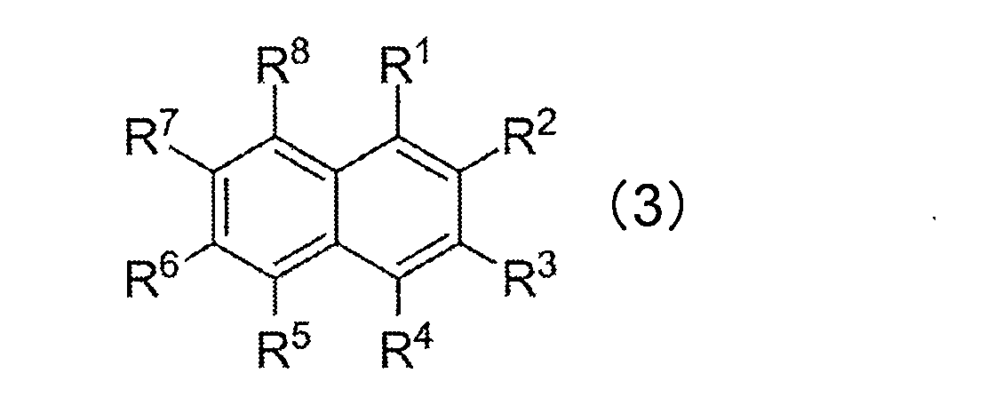
- A is a group represented by the general formula (3)
- B is an alkoxy group, alkylthio group, aryl ether group, aryl thioether group, amino group, furanyl group, thiophenyl group, pyrrolyl group, benzofuranyl group, benzothiophenyl group, indolyl group, dibenzofuranyl group, dibenzothiophenyl group and carbazolyl
- C is an aromatic heterocyclic group containing an electron-accepting nitrogen or a group selected from the group consisting of an alkyl group, a cycloalkyl group, an alkenyl group, a cycloalkenyl group, an alkynyl group, an aryl group, and a heteroaryl group.
- m and n each represents an integer of 1 to 4.
- R 1 to R 8 may be the same or different and each is a group selected from the group consisting of hydrogen, an alkyl group, a cycloalkyl group, an alkenyl group, a cycloalkenyl group, an alkynyl group, and an aryl group.
- adjacent groups may be bonded to each other to form a single ring or a condensed ring.
- R 1 ⁇ R 8 and monocyclic or condensed ring any adjacent group is formed by bonding of R 1 ⁇ R 8, in either the m position of coupled by B
- any single ring or condensed ring adjacent group is formed by bonding, either the n of R 1 ⁇ R 8, and R 1 ⁇ R 8 It connects with C in the position of.
- a in General formula (1) and A in General formula (2) are the same groups.
- a photoelectric conversion element that exhibits high color selectivity, a low dark current, and high photoelectric conversion efficiency can be provided.
- the schematic cross section which shows an example of the photoelectric conversion element of this invention The schematic cross section which shows an example of the photoelectric conversion element of this invention.
- the photoelectric conversion element of the present invention is a photoelectric conversion element in which at least one organic layer is present between the first electrode and the second electrode, and converts light into electric energy. It contains a compound represented by 1) and a compound represented by the general formula (2).
- Both the compound represented by the general formula (1) and the compound represented by the general formula (2) are preferable in that they have a high light absorption coefficient in the visible region.
- the visible region is a range of wavelengths from 400 nm to 700 nm.
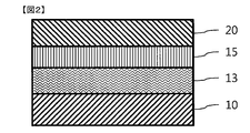
- FIG. 1 is an example of a photoelectric conversion element having a first electrode 10 and a second electrode 20 and at least one organic layer 15 interposed therebetween.
- the organic layer includes a photoelectric conversion layer that converts light into electrical energy.
- first electrode 10 is a cathode and the second electrode 20 is an anode will be described as an example.
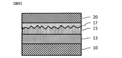
- a charge blocking layer may be inserted between the cathode and the anode as shown in FIGS.
- the charge blocking layer is a layer having a function of blocking electrons or holes, and is inserted between the anode and the photoelectric conversion layer as the electron blocking layer 13 when inserted between the cathode and the photoelectric conversion layer. In this case, it functions as a hole blocking layer 17.
- the photoelectric conversion element may contain only one kind of these layers, or may contain both.
- the photoelectric conversion layer may be a single layer in which two or more types of photoelectric conversion materials are mixed, or each layer is composed of one or more types of photoelectric conversion materials.
- a plurality of layers may be laminated. Furthermore, the structure by which the mixed layer and each single layer were laminated
- A is a group represented by the general formula (3)
- B is an alkoxy group, alkylthio group, aryl ether group, aryl thioether group, amino group, furanyl group, thiophenyl group, pyrrolyl group, benzofuranyl group, benzothiophenyl group, indolyl group, dibenzofuranyl group, dibenzothiophenyl group and carbazolyl
- C is an aromatic heterocyclic group containing an electron-accepting nitrogen or a group selected from the group consisting of an alkyl group, a cycloalkyl group, an alkenyl group, a cycloalkenyl group, an alkynyl group, an aryl group, and a heteroaryl group.
- m and n each represents an integer of 1 to 4.
- R 1 to R 8 may be the same or different and each is a group selected from the group consisting of hydrogen, an alkyl group, a cycloalkyl group, an alkenyl group, a cycloalkenyl group, an alkynyl group, and an aryl group.
- adjacent groups may be bonded to each other to form a single ring or a condensed ring.
- R 1 ⁇ R 8 and monocyclic or condensed ring any adjacent group is formed by bonding of R 1 ⁇ R 8, in either the m position of coupled by B
- any single ring or condensed ring adjacent group is formed by bonding, either the n of R 1 ⁇ R 8, and R 1 ⁇ R 8 It connects with C in the position of.
- a in General formula (1) and A in General formula (2) are the same groups.
- the alkyl group represents, for example, a saturated aliphatic hydrocarbon group such as a methyl group, an ethyl group, an n-propyl group, an isopropyl group, an n-butyl group, a sec-butyl group, or a tert-butyl group. It may or may not have a substituent.
- a substituent There is no restriction
- the number of carbon atoms of the alkyl group is not particularly limited, but is usually in the range of 1 to 20 and more preferably 1 to 8 from the viewpoint of availability and cost.
- the cycloalkyl group represents, for example, a saturated alicyclic hydrocarbon group such as cyclopropyl, cyclohexyl, norbornyl, adamantyl, etc., which may or may not have a substituent.
- carbon number of an alkyl group part is not specifically limited, Usually, it is the range of 3-20.
- alkenyl group refers to an unsaturated aliphatic hydrocarbon group containing a double bond such as a vinyl group, an allyl group, or a butadienyl group, which may or may not have a substituent.
- carbon number of an alkenyl group is not specifically limited, Usually, it is the range of 2-20.
- the cycloalkenyl group refers to an unsaturated alicyclic hydrocarbon group containing a double bond such as a cyclopentenyl group, a cyclopentadienyl group, or a cyclohexenyl group, which may have a substituent. You don't have to. Although carbon number of a cycloalkenyl group is not specifically limited, Usually, it is the range of 2-20.
- the alkynyl group indicates, for example, an unsaturated aliphatic hydrocarbon group containing a triple bond such as an ethynyl group, which may or may not have a substituent.
- carbon number of an alkynyl group is not specifically limited, Usually, it is the range of 2-20.
- An aryl group refers to an aromatic hydrocarbon group such as a phenyl group, a naphthyl group, a biphenyl group, a fluorenyl group, a phenanthryl group, a triphenylenyl group, or a terphenyl group.
- the aryl group may or may not have a substituent. Although carbon number of an aryl group is not specifically limited, Usually, it is the range of 6-40.
- An alkoxy group refers to a functional group in which an aliphatic hydrocarbon group is bonded through an ether bond such as a methoxy group, an ethoxy group, or a propoxy group. This aliphatic hydrocarbon group may or may not have a substituent. Although carbon number of an alkoxy group is not specifically limited, Usually, it is the range of 1-20.
- the alkylthio group is a group in which an oxygen atom of an ether bond of an alkoxy group is substituted with a sulfur atom.
- the hydrocarbon group of the alkylthio group may or may not have a substituent. Although carbon number of an alkylthio group is not specifically limited, Usually, it is the range of 1-20.
- An aryl ether group refers to a functional group to which an aromatic hydrocarbon group is bonded via an ether bond, such as a phenoxy group, and the aromatic hydrocarbon group may or may not have a substituent. Good. Although carbon number of an aryl ether group is not specifically limited, Usually, it is the range of 6-40.
- the aryl thioether group is a group in which an oxygen atom of an ether bond of an aryl ether group is substituted with a sulfur atom.
- the aromatic hydrocarbon group in the aryl ether group may or may not have a substituent. Although carbon number of an aryl ether group is not specifically limited, Usually, it is the range of 6-40.
- the amino group may or may not have a substituent, and examples of the substituent include an aryl group and a heteroaryl group, and these substituents may be further substituted.
- the furanyl group may or may not have a substituent, and examples of the substituent include an alkyl group, an aryl group, and a heteroaryl group, and these substituents may be further substituted. .
- the thiophenyl group may or may not have a substituent.
- substituents include an alkyl group, an aryl group, and a heteroaryl group, and these substituents may be further substituted. .
- the pyrrolyl group may or may not have a substituent.
- substituents include an alkyl group, an aryl group, and a heteroaryl group, and these substituents may be further substituted. .
- the benzofuranyl group may or may not have a substituent, and examples of the substituent include an alkyl group, an aryl group, and a heteroaryl group, and these substituents may be further substituted. .
- the benzothiophenyl group may or may not have a substituent, and examples of the substituent include an alkyl group, an aryl group, and a heteroaryl group, and these substituents are further substituted. Also good.
- the indolyl group may or may not have a substituent.
- substituents include an alkyl group, an aryl group, and a heteroaryl group, and these substituents may be further substituted. .
- the dibenzofuranyl group may or may not have a substituent, and examples of the substituent include an alkyl group, an aryl group, and a heteroaryl group, and these substituents are further substituted. Also good.
- the dibenzothiophenyl group may or may not have a substituent, and examples of the substituent include an alkyl group, an aryl group, and a heteroaryl group, and these substituents are further substituted. Also good.
- the carbazolyl group may or may not have a substituent, and examples of the substituent include an alkyl group, an aryl group, and a heteroaryl group, and these substituents may be further substituted. .
- a heteroaryl group is one or more atoms other than carbon such as furanyl, thiophenyl, pyridyl, quinolinyl, pyrazinyl, pyrimidinyl, triazinyl, naphthyridyl, benzofuranyl, benzothiophenyl, indolyl, etc.
- the cyclic aromatic group which has in an individual ring is shown, This may be unsubstituted or substituted.
- carbon number of heteroaryl group is not specifically limited, Usually, it is the range of 2-30.
- Halogen means fluorine, chlorine, bromine and iodine.
- R 1 ⁇ R 8 In any position of R 1 ⁇ R 8 and connects the B or C refers to a carbon atom and B or C of the root of R 1 ⁇ R 8 is attached at the naphthalene ring of A is directly bonded.
- Linking to B or C at any position of a monocyclic ring or condensed ring formed by bonding any adjacent groups of R 1 to R 8 to each other constitutes the mother skeleton of the monocyclic ring or condensed ring
- any carbon atom and B or C are directly bonded.
- R 2 and R 3 are bonded to each other to form a 6-membered ring
- any one or more of four carbon atoms that can be bonded to another atom in the 6-membered ring and B or C Is the case where is directly coupled.
- the compound represented by the general formula (1) has a group represented by B in the molecule.
- the groups represented by B are as described above, and these are electron donating groups.
- the compound represented by the general formula (1) has a high hole transporting property by including B which is an electron donating property in the molecule. Therefore, holes generated in the photoelectric conversion layer can be efficiently carried to the electrode side, and high photoelectric conversion efficiency can be obtained.
- B when B is contained in the molecule, the intermolecular interaction is suppressed and the width of the absorption spectrum is narrowed. Therefore, the selectivity of the absorption wavelength is improved. In addition, since aggregation of molecules can be prevented, high photoelectric conversion efficiency stable over time can be obtained.
- B is an amino group, furanyl group, thiophenyl group, pyrrolyl group, benzofuranyl group, benzothiophenyl group, indolyl group, dibenzofuranyl group, dibenzothiophenyl group and carbazolyl group, phenoxy group, methoxy group, methylthio group and phenylthio group.
- B is more preferably a benzofuranyl group, a benzothiophenyl group, an indolyl group, a dibenzofuranyl group, a phenoxy group, a methoxy group, a methylthio group, and a phenylthio group, more preferably a benzofuranyl group, a benzothiophenyl group, and an indolyl group.
- the group is particularly preferred.
- each B may be the same or different.
- the compound represented by the general formula (2) has a group represented by C in the molecule. Although the group which C shows is as above-mentioned, these are electron-accepting groups.
- the compound represented by the general formula (2) has a high electron transport property by containing C, which is an electron accepting group, in the molecule. Therefore, electrons generated in the photoelectric conversion layer can be efficiently carried to the electrode side, and high photoelectric conversion efficiency can be obtained. Furthermore, in the compound represented by the general formula (2), when C is contained in the molecule, the intermolecular interaction is suppressed and the width of the absorption spectrum is narrowed. Therefore, the selectivity of the absorption wavelength is improved. In addition, since aggregation of molecules can be prevented, high photoelectric conversion efficiency stable over time can be obtained.
- C is preferably an aromatic heterocyclic group containing an electron-accepting nitrogen, or an alkyl group, an alkenyl group, an aryl group or a heteroaryl group, which is substituted with a halogen or a cyano group.
- the maximum absorption wavelength of the compound represented by the general formula (2) can be arbitrarily selected.
- a pyrimidyl group is preferable as the aromatic heterocyclic group containing electron-accepting nitrogen.
- the aryl group here is preferably a phenyl group.
- the heteroaryl group here is preferably a pyrimidyl group.
- C is preferably an alkenyl group, an aryl group or a heteroaryl group, which is substituted with a cyano group, a group represented by —CH ⁇ C (CN) 2 , a phenyl substituted with a cyano group And a pyrimidyl group substituted with a cyano group is particularly preferred.
- C is an alkyl group or an aryl group and is substituted with a halogen, more preferably one substituted with fluorine because it has the highest electron accepting property, and phenyl substituted with fluorine.
- the group is particularly preferred.
- each C may be the same or different.
- R 1 to R 8 may be any group selected from hydrogen, alkyl groups, cycloalkyl groups, alkenyl groups, cycloalkenyl groups, alkynyl groups, and aryl groups. From the viewpoint of facilitating vacuum deposition, it is preferable that substituents are appropriately combined so that the molecular weight of the compound represented by the general formula (1) and the compound represented by the general formula (2) is 300 to 700. . Among these groups, hydrogen is preferable because it can easily obtain a narrow half width in the absorption spectrum.
- R 1 to R 8 are bonded to any adjacent groups (for example, R 1 and R 2 in the general formula (3)) to form a conjugated condensed ring. May be.
- the skeleton represented by the general formula (3) greatly contributes to the improvement of charge transportability by the formation of ⁇ electron interaction. And the improvement effect of charge transport property becomes remarkable because the number of rings of the formed condensed ring becomes three or more as a whole. Moreover, if it is a condensed ring of 3 or more rings, it becomes possible to have an absorption wavelength in the visible region and a high charge transport property.
- A is a condensed ring composed of 3 to 6 rings as a whole, and more preferably, A is a condensed ring composed of 4 to 6 rings as a whole. More preferably, A forms a condensed ring having 4 to 5 rings in total, and particularly preferably A forms a condensed ring having 4 rings in total.
- carbon is preferable because it is a material capable of transporting both holes and electrons.
- it is not limited to this, but includes an element selected from nitrogen, oxygen, sulfur, phosphorus and silicon in addition to carbon A configuration may be taken.
- the condensed ring may be further condensed with another ring.
- Examples of the skeleton represented by the general formula (3) include ring structures such as anthracene, phenanthrene, naphthacene, pyrene, chrysene, triphenylene, fluoranthene, benzofluoranthene, perylene, pentacene, and hexacene. It is not limited.
- the connecting positions of the substituent B and the substituent C may be any positions as long as they are connected to a bondable carbon atom, but the following skeleton bonds are shown from the viewpoint of ease of synthesis. Of the positions, it is preferable to use the location a.
- the number m of the substituents B and the number n of the substituents C bonded to the skeleton represented by the general formula (3) are not particularly limited, but are usually in the range of 1 to 8.
- the absorption spectra of the compounds represented by the general formula (1) and the general formula (2) become longer. Therefore, by adjusting the number of substituents B and C, it is possible to arbitrarily select the maximum absorption wavelength of the compounds represented by general formula (1) and general formula (2).
- M and n are preferably set so that the absorption spectra of the compounds represented by the general formula (1) and the general formula (2) are in the same wavelength range from the viewpoint of improving color selectivity.
- the same wavelength range does not need to be exactly the same.
- the difference between the maximum value of the compound represented by the general formula (1) and the maximum value of the absorption spectrum of the compound represented by the general formula (2) is preferably 50 nm or less.
- M is more preferably 1 to 3, and even more preferably 3.
- n is more preferably 1 to 3, and still more preferably 1.
- the respective substituents may be of the same type or different types.
- pyrene, perylene, pentacene, and hexacene are preferable because of their good charge transporting ability.
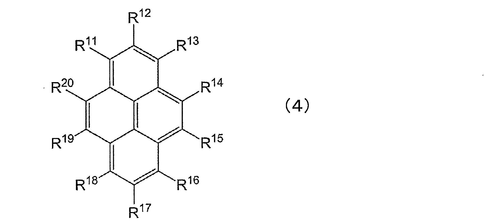
- pyrene represented by the general formula (4) is easy to synthesize, has a high light absorption coefficient, and is excellent. From the viewpoint of the wavelength selectivity, it is mentioned as a preferable skeleton.
- R 11 to R 20 in the general formula (4) may be the same or different and are selected from the group consisting of hydrogen, an alkyl group, a cycloalkyl group, an alkenyl group, a cycloalkenyl group, an alkynyl group, and an aryl group. Group.
- adjacent groups may be bonded to each other to form a single ring or a condensed ring.
- the substituent B and the substituent C may be arranged at any position among R 11 to R 20 of the pyrene skeleton represented by the general formula (4). However, R 11 , R 13 , It is preferably substituted at at least one position of R 16 and R 18 or at least one position of R 12 and R 17 . Further, when the positions of the substituent B and the substituent C are arranged in R 11 , R 13 , R 16 , and R 18 , the electron cloud spreads more favorably, so that the charge transport property is improved.
- the number of substituents arranged on the pyrene skeleton is arbitrarily set according to the target absorption wavelength. Since the molecular weight of the compound is set to be 300 to 700 so as to facilitate vacuum deposition, it is usually 1 or more and 4 or less including the number of B and C.
- R 11 to R 20 are preferably hydrogen or an aryl group.
- R 11 , R 13 , R 16 and R 18 which is not the substituent B and the substituent C (hereinafter referred to as “remaining R”) is hydrogen or an aryl group. Further, it is particularly preferable that all remaining Rs are hydrogen.
- the compound represented by the general formula (1) and the compound represented by the general formula (2) may be contained in any layer of the organic layer in the photoelectric conversion element, but the organic layer is a plurality of layers. Preferably, both of the compound represented by the general formula (1) and the compound represented by the general formula (2) are included in one of them.
- the layer is preferably a bulk heterojunction layer composed of the compound represented by the general formula (1) and the compound represented by the general formula (2).
- the bulk heterojunction layer will be described later.
- the layer preferably has a mixing ratio of the compound represented by the general formula (1) and the compound represented by the general formula (2) of 1: 3 to 3: 1.
- the configuration of the photoelectric conversion layer is a bulk heterojunction layer in which the compound represented by the general formula (1) and the compound represented by the general formula (2) are mixed in the same layer by a method such as co-evaporation. Is preferred.
- the photoelectric conversion layer can form a stable amorphous structure.
- the bulk heterojunction layer is a structure in which two or more compounds are randomly mixed in one layer and the compounds are joined at the nano level.
- Amorphous is a non-crystalline structure with a flat thin film surface. Then, by forming a stable amorphous structure in the photoelectric conversion layer, it is possible to reduce a current (referred to as “dark current”) that flows when the photoelectric conversion element is not irradiated with light. When the dark current is reduced, the contrast between the current that flows during light irradiation (referred to as “photocurrent”) and the dark current increases, so that a high-performance imaging device with less noise can be realized.
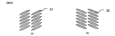
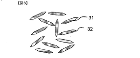
- FIG. 5 to FIG. 7 are schematic views showing the orientation state of compound molecules in the photoelectric conversion film.
- FIG. 8 is a schematic cross-sectional view of the photoelectric conversion element.
- the bulk heterojunction layer is represented by the general formula (1).
- the compound represented by the general formula (2) has the same skeleton, the substituents are different from each other, so that it is difficult to form an aggregated structure.
- an amorphous photoelectric conversion film is formed.
- the film surface has a flat structure as shown in FIG. 4, so that a uniform electric field is applied to the entire photoelectric conversion film in the photoelectric conversion element, and dark current can be reduced. It becomes.
- the mixing ratio of the compound represented by the general formula (1) and the compound represented by the general formula (2) is expressed as a molar ratio (represented by the general formula (1) from the viewpoint of the transport balance between holes and electrons.
- the charge mobility (namely, hole mobility) of the compound represented by the general formula (1) and the charge mobility (namely, electron mobility) of the compound represented by the general formula (2) are 1 ⁇ 10 ⁇ 9 , respectively. It is preferably at least cm 2 / Vs, more preferably at least 1 ⁇ 10 ⁇ 8 cm 2 / Vs, and even more preferably at least 1 ⁇ 10 ⁇ 7 cm 2 / Vs.
- the charge mobility in this specification is the mobility measured by the space charge limited current method (SCLC method).
- SCLC method space charge limited current method
- the thickness of the organic layer is preferably 20 nm or more and 200 nm or less from the viewpoint of suppressing current leakage and reducing power consumption.
- the shape of the absorption spectrum of the organic thin film varies greatly depending on the type of skeleton, but the compound represented by the general formula (1) and the compound represented by the general formula (2) Since they have the structure of the general formula (3) having the same skeleton, the shape of each absorption spectrum is almost similar. Therefore, as in the present invention, when the photoelectric conversion layer includes both the compound represented by the general formula (1) and the compound represented by the general formula (2), the shape of the absorption spectrum becomes sharp, Color selectivity can be improved.
- red light indicates a wavelength region of approximately 580 to 720 nm
- green light indicates a wavelength region of approximately 480 to 620
- blue light indicates a wavelength region of approximately 380 to 520 nm.
- the absorption spectrum of the photoelectric conversion layer containing both the compound represented by the general formula (1) and the compound represented by the general formula (2) -It is preferable to exist in each wavelength region of green light and blue light.
- the absorption spectrum of the photoelectric conversion layer is preferably in the wavelength region of approximately 580 to 720 nm.
- the wavelength is approximately 480 to 620 in the case of green light and approximately 380 to 520 nm in the case of blue light.
- the half value width of the absorption spectrum of the photoelectric converting layer containing the compound represented by General formula (1) and the compound represented by General formula (2) is 120 nm or less, and is 100 nm or less. Is more preferable.
- the half-value widths of the absorption spectra of the compound represented by the general formula (1) and the compound represented by the general formula (2) are both from the viewpoint of achieving both good color selectivity and color reproducibility. It is preferably 25 nm or more and 100 nm or less, and more preferably 40 nm or more and 100 nm or less.
- the difference between the maximum value of the absorption spectrum of the compound represented by the general formula (1) and the maximum value of the absorption spectrum of the compound represented by the general formula (2) is preferably 50 nm or less, and 40 nm or less. More preferably. Thereby, the peak of an absorption spectrum becomes single and color selectivity improves.
- a photoelectric conversion layer is a layer in which photoelectric conversion that absorbs incident light and generates charges occurs. This may be composed of a single photoelectric conversion material, but is preferably composed of a p-type semiconductor material and an n-type semiconductor material. At this time, each of the p-type semiconductor material and the n-type semiconductor material may be single or plural.
- the photoelectric conversion layer after the photoelectric conversion material absorbs light and forms excitons, electrons and holes are separated by an n-type semiconductor material and a p-type semiconductor material, respectively. The separated electrons and holes flow to the both poles through the conduction level and the valence level, respectively, and generate electric energy.
- the compound represented by the general formula (1) and the compound represented by the general formula (2) have a high light absorption coefficient and a high charge transport property in the visible region, they are particularly suitable for the photoelectric conversion layer among the organic layers. It is preferable to be used. Furthermore, the photoelectric conversion layer is composed of two or more types of photoelectric conversion element materials, and two of them are a compound represented by the general formula (1) and a compound represented by the general formula (2). Is preferred.
- the compound represented by the general formula (1) is preferably used as a p-type semiconductor material.
- the compound represented by (2) is preferably used as an n-type semiconductor material. Since the compound represented by the general formula (1) contains B which is an electron donating property in the molecule, it has the property of transporting holes more than electrons, and the compound represented by the general formula (2) This is because, since C containing electron-accepting is contained in the molecule, it has the property of transporting electrons more easily than holes.
- the n-type semiconductor material refers to an electron-transporting semiconductor material having an electron accepting property and a property of easily receiving electrons (high electron affinity).
- the p-type semiconductor material refers to a hole-transporting semiconductor material having an electron donating property and a property of easily releasing electrons (low ionization potential).
- the ionization potential of the compound represented by the general formula (1) is represented as Ip 1
- the electron affinity is represented as Ea 1
- the ionization potential of the compound represented by the general formula (2) is represented as Ip 2
- the electron affinity is represented as Ea 2 .
- Ip 1 ⁇ Ip 2 and Ea 1 ⁇ Ea 2 it is preferable that Ip 1 ⁇ Ip 2 and Ea 1 ⁇ Ea 2 .
- the ionization potential is defined as the energy difference between the occupied energy orbit with the highest energy among the molecular orbitals of the compound and the vacuum level, and the value is measured using ultraviolet photoelectron spectroscopy.
- the electron affinity is defined as the energy difference between the lowest orbital empty orbit and the vacuum level among the molecular orbitals of the compound, and is obtained from the difference between the measured value of the ionization potential and the measured value of the band gap.
- the photoelectric conversion element of the present invention is not limited to a structure in which the photoelectric conversion layer includes only the compound represented by the general formula (1) and the compound represented by the general formula (2).
- the electron blocking layer may include the compound represented by the general formula (1).
- a compound represented by the general formula (1) and a compound represented by the general formula (2) are added to the photoelectric conversion layer.
- the structure which contains both and the compound represented by General formula (2) in a hole-blocking layer may be sufficient.
- the electron blocking layer and the hole blocking layer contain both the compound represented by the general formula (1) and the compound represented by the general formula (2) for the purpose of improving the light absorption of the entire device. May be.
- the photoelectric conversion material constituting the photoelectric conversion layer is preferably composed of only the compound represented by the above general formula (1) and the compound represented by the general formula (2), but is not limited thereto.
- the photoelectric conversion layer may further include a material that has been known as a photoelectric conversion material.
- the p-type semiconductor material may be any organic compound as long as it has a relatively small ionization potential, an electron donating property, and a hole transporting compound.
- p-type organic semiconductor materials include compounds having derivatives such as naphthalene, anthracene, phenanthrene, pyrene, chrysene, naphthacene, triphenylene, perylene, fluoranthene, fluorene, indene, derivatives thereof, cyclopentadiene derivatives, furan Derivatives, thiophene derivatives, pyrrole derivatives, benzofuran derivatives, benzothiophene derivatives, indole derivatives, pyrazoline derivatives, dibenzofuran derivatives, dibenzothiophene derivatives, carbazole derivatives, indolocarbazole derivatives, N, N'-dinaphthyl-N, N'-diphenyl- Aromatic amine derivatives such as 4,4
- polystyrene resin examples include, but are not limited to, polyphenylene vinylene derivatives, polyparaphenylene derivatives, polyfluorene derivatives, polyvinylcarbazole derivatives, and polythiophene derivatives.
- the above material group can be used, but is not particularly limited.
- the n-type semiconductor material may be any material as long as it has a high electron affinity and is an electron transporting compound.
- n-type semiconductor materials include condensed polycyclic aromatic derivatives such as naphthalene and anthracene, styryl aromatic ring derivatives represented by 4,4′-bis (diphenylethenyl) biphenyl, tetraphenylbutadiene derivatives, coumarin derivatives, Oxadiazole derivatives, pyrrolopyridine derivatives, perinone derivatives, pyrrolopyrrole derivatives, thiadiazolopyridine derivatives, aromatic acetylene derivatives, aldazine derivatives, pyromethene derivatives, diketopyrrolo [3,4-c] pyrrole derivatives, imidazoles, thiazoles, thiadiazoles, Azole derivatives such as oxazole, oxadiazole, triazole and metal complexes thereof, quinone derivatives such
- organic compounds having a nitro group, cyano group, halogen or trifluoromethyl group in the molecule include fullerene derivatives.
- the electron-accepting nitrogen mentioned here represents a nitrogen atom forming a multiple bond with an adjacent atom. Since the nitrogen atom has a high electronegativity, the multiple bond has an electron accepting property. Therefore, an aromatic heterocycle containing electron-accepting nitrogen has high electron affinity and is preferable as an n-type semiconductor material.
- heteroaryl ring containing an electron-accepting nitrogen examples include, for example, a pyridine ring, pyrazine ring, pyrimidine ring, quinoline ring, quinoxaline ring, naphthyridine ring, pyrimidopyrimidine ring, benzoquinoline ring, phenanthroline ring, imidazole ring, oxazole ring, Examples thereof include an oxadiazole ring, a triazole ring, a thiazole ring, a thiadiazole ring, a benzoxazole ring, a benzothiazole ring, a benzimidazole ring, and a phenanthrimidazole ring.
- Examples of these compounds having a heteroaryl ring structure include benzimidazole derivatives, benzoxazole derivatives, benzthiazole derivatives, oxadiazole derivatives, thiadiazole derivatives, triazole derivatives, pyrazine derivatives, phenanthroline derivatives, quinoxaline derivatives, quinoline derivatives, benzoins.
- Preferred compounds include quinoline derivatives, oligopyridine derivatives such as bipyridine and terpyridine, quinoxaline derivatives and naphthyridine derivatives.
- imidazole derivatives such as tris (N-phenylbenzimidazol-2-yl) benzene, oxadiazole derivatives such as 1,3-bis [(4-tert-butylphenyl) 1,3,4-oxadiazolyl] phenylene, Triazole derivatives such as N-naphthyl-2,5-diphenyl-1,3,4-triazole, phenanthroline derivatives such as bathocuproine and 1,3-bis (1,10-phenanthroline-9-yl) benzene, 2,2 ′
- a benzoquinoline derivative such as bis (benzo [h] quinolin-2-yl) -9,9′-spirobifluorene, 2,5-bis (6 ′-(2 ′, 2 ′′ -bipyridyl))-1, Bipyridine derivatives such as 1-dimethyl-3,4-diphenylsilole, 1,3-bis (4 ′-(2,2 )
- the above-mentioned material group can be used, but is not particularly limited.
- the cathode and the anode have a role for allowing electrons and holes generated in the element to flow and sufficiently flowing current. It is desirable that at least one of these is transparent or translucent in order to allow light to enter the photoelectric conversion layer.
- the cathode formed on the substrate is preferably a transparent electrode.
- the cathode may be any transparent material that can efficiently extract holes from the photoelectric conversion layer.
- Materials include conductive metal oxides such as tin oxide, indium oxide and indium tin oxide (ITO), metals such as gold, silver and chromium, inorganic conductive materials such as copper iodide and copper sulfide, polythiophene, polypyrrole, Conductive polymers such as polyaniline are preferred, and ITO glass or Nesa glass is particularly preferred.
- the resistance of the transparent electrode only needs to be sufficient to allow a current generated by the element to flow, and is preferably a low resistance from the viewpoint of photoelectric conversion efficiency of the element.
- an ITO substrate having a resistance of 300 ⁇ / ⁇ or less functions as an element electrode, so that it is particularly preferable to use a low resistance product.
- the thickness of ITO can be arbitrarily selected according to the resistance value, but is usually used in a range of 50 to 300 nm.
- the ITO film forming method is not particularly limited, such as an electron beam method, a sputtering method, or a chemical reaction method.
- the glass substrate soda lime glass, non-alkali glass, or the like is used, and it is sufficient that the thickness is sufficient to maintain the mechanical strength, so 0.5 mm or more is sufficient.
- the glass material is preferably alkali-free glass because it is better that there are fewer ions eluted from the glass, and soda lime glass with a barrier coating such as SiO 2 can also be used.
- the cathode functions stably, the substrate does not have to be glass.
- the anode may be formed on a plastic substrate.
- the anode is preferably a substance that can efficiently extract electrons from the photoelectric conversion layer. Platinum, gold, silver, copper, iron, tin, zinc, aluminum, indium, chromium, lithium, sodium, potassium, calcium, magnesium, cesium, strontium Etc. Low work function metals such as lithium, sodium, potassium, calcium, magnesium, and cesium or alloys containing these are effective for improving the device characteristics by increasing the electron extraction efficiency.
- a method in which a compound used as a hole blocking layer described later is doped with a small amount of lithium, magnesium, or cesium (1 nm or less in a vacuum vapor deposition thickness meter display) is used as a highly stable anode. Can be mentioned.
- inorganic salts such as lithium fluoride can be used.
- metals such as platinum, gold, silver, copper, iron, tin, aluminum, indium, or alloys using these metals, and inorganic substances such as silica, titania, silicon nitride, polyvinyl alcohol, vinyl chloride, It is preferable to laminate a hydrocarbon polymer or the like.
- a resistance heating method As the electrode manufacturing method, a resistance heating method, an electron beam beam method, a sputtering method, an ion plating method, a coating method and the like are preferable.
- the photoelectric conversion element When used as an image sensor, it is preferable to apply an electric field from the outside so that the cathode has a negative potential with respect to the anode. This is because the electrons generated in the photoelectric conversion layer are easily guided to the anode side and the holes are easily guided to the cathode side, so that an effect of improving the photoelectric conversion efficiency occurs. Therefore, the photoelectric conversion element preferably includes a voltage application unit that applies a voltage to the organic layer.
- the applied voltage is preferably 10 5 V / m or more and 10 9 V / m or less from the viewpoint of improving photoelectric conversion efficiency and suppressing current leakage.
- the charge blocking layer is a layer used to efficiently and stably take out electrons and holes photoelectrically converted in the photoelectric conversion layer from the electrode, and an electron blocking layer that blocks electrons and a hole that blocks holes. And a blocking layer. These may be comprised from the inorganic substance and may be comprised from the organic compound. Furthermore, you may consist of a mixed layer of an inorganic substance and an organic compound.
- the hole blocking layer is a layer for blocking holes generated in the photoelectric conversion layer from flowing to the anode side and recombining with electrons. Depending on the type of material constituting each layer, insertion of this layer suppresses recombination of holes and electrons and improves photoelectric conversion efficiency. Therefore, the hole blocking material preferably has a HOMO level lower in energy than the photoelectric conversion material.
- a compound that can efficiently block the movement of holes from the photoelectric conversion layer is preferable.
- quinolinol derivative metal complexes represented by 8-hydroxyquinoline aluminum, tropolone metal complexes, flavonol metal complexes, perylene derivatives, perinone derivatives examples include naphthalene derivatives, coumarin derivatives, oxadiazole derivatives, aldazine derivatives, bisstyryl derivatives, pyrazine derivatives, oligopyridine derivatives such as bipyridine and terpyridine, phenanthroline derivatives, quinoline derivatives, and aromatic phosphorus oxide compounds.
- These hole blocking materials are used alone, but may be used by being laminated or mixed with different hole blocking materials.
- the electron blocking layer is a layer for blocking electrons generated in the photoelectric conversion layer from flowing to the cathode side and recombining with holes.
- the electron blocking material preferably has an LUMO level higher in energy than the photoelectric conversion material.
- the above hole-blocking layer and electron-blocking layer may be used alone or in combination of two or more materials, or polyvinyl chloride, polycarbonate, polystyrene, poly (N-vinylcarbazole), polymethyl methacrylate as a polymer binder.
- Solvent soluble resins such as polybutyl methacrylate, polyester, polysulfone, polyphenylene oxide, polybutadiene, hydrocarbon resin, ketone resin, phenoxy resin, polysulfone, polyamide, ethyl cellulose, vinyl acetate, ABS resin, polyurethane resin, phenol resin, xylene
- the resin, petroleum resin, urea resin, melamine resin, unsaturated polyester resin, alkyd resin, epoxy resin, curable resin such as silicone resin, and the like can also be used by being dispersed.
- the method for forming the organic layer is not particularly limited, such as resistance heating vapor deposition, electron beam vapor deposition, sputtering, molecular lamination method, and coating method, but resistance heating vapor deposition and electron beam vapor deposition are usually preferred in terms of characteristics.
- An image sensor is a semiconductor element that converts an optical image into an electrical signal.
- an image sensor includes the photoelectric conversion element that converts light into electric energy and a circuit that reads the electric energy into an electric signal.
- a plurality of photoelectric conversion elements can be arranged in a one-dimensional straight line or a two-dimensional plane.
- a mono-color image sensor it may be composed of one type of photoelectric conversion element.
- a color image sensor it is composed of two or more types of photoelectric conversion elements, such as a photoelectric conversion element that detects red light, a photoelectric conversion element that detects green light, and a photoelectric conversion element that detects blue light.
- the photoelectric conversion elements of the respective colors have a stacked structure, that is, may be stacked in one pixel, or may be configured in a matrix structure side by side.
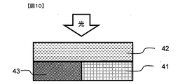
- a photoelectric conversion element 42 that detects green light, a photoelectric conversion element 43 that detects blue light, and a red light are detected.
- a three-layer structure in which the photoelectric conversion elements 41 are sequentially stacked may be used.
- a photoelectric conversion element 42 for detecting green light is arranged on the entire upper surface, the photoelectric conversion element 41 for detecting red light, and blue light is detected.
- the photoelectric conversion element 43 to be formed may have a two-layer structure formed in a matrix structure. In these structures, a photoelectric conversion element that detects green light is arranged in a layer closest to incident light.
- each color is not limited to these, and may be different from that shown in FIG.
- a matrix structure In the case of a matrix structure, it can be selected from an array such as a Bayer array, a honeycomb array, a stripe array, or a delta array.
- an organic photoelectric conversion material is used for the photoelectric conversion element that detects green light, and the photoelectric conversion element that detects red light and the photoelectric conversion element that detects blue light are conventionally used inorganic photoelectric conversion materials. Or organic photoelectric conversion materials may be used in appropriate combination.
- the image sensor of the present invention is composed of two or more types of photoelectric conversion elements, and at least one of them is preferably the above-described photoelectric conversion element.
- the two or more types of photoelectric conversion elements preferably have a laminated structure.
- the photoelectric conversion layer composed of the compound represented by the general formula (1) and the compound represented by the general formula (2) is excellent in the ability to selectively detect a specific wavelength region.
- the image sensor of the present invention is configured by photoelectric conversion elements that detect red light, green light, and blue light, and at least one type of photoelectric conversion element in the stacked structure detects light of these colors.
- a photoelectric conversion element is preferable.
- the ionization potential of the compounds used in this example and comparative examples was measured using AC-2 (manufactured by Riken Keiki Co., Ltd.).
- the electron affinity was calculated by using an absorption spectrum measured with a U-3200 spectrophotometer (manufactured by Hitachi, Ltd.).
- a glass substrate manufactured by Asahi Glass Co., Ltd., 15 ⁇ / ⁇ , electron beam evaporated product
- ITO transparent conductive film was deposited to 150 nm was cut into 30 ⁇ 40 mm and etched.
- the obtained substrate was ultrasonically washed with acetone and “Semicoclean (registered trademark) 56” (manufactured by Furuuchi Chemical Co., Ltd.) for 15 minutes, respectively, and then washed with ultrapure water. Subsequently, it was ultrasonically cleaned with isopropyl alcohol for 15 minutes and then immersed in hot methanol for 15 minutes and dried. This substrate was treated with UV-ozone for 1 hour immediately before producing the device.
- PEDOT / PSS Lithm TM PVP AI4083
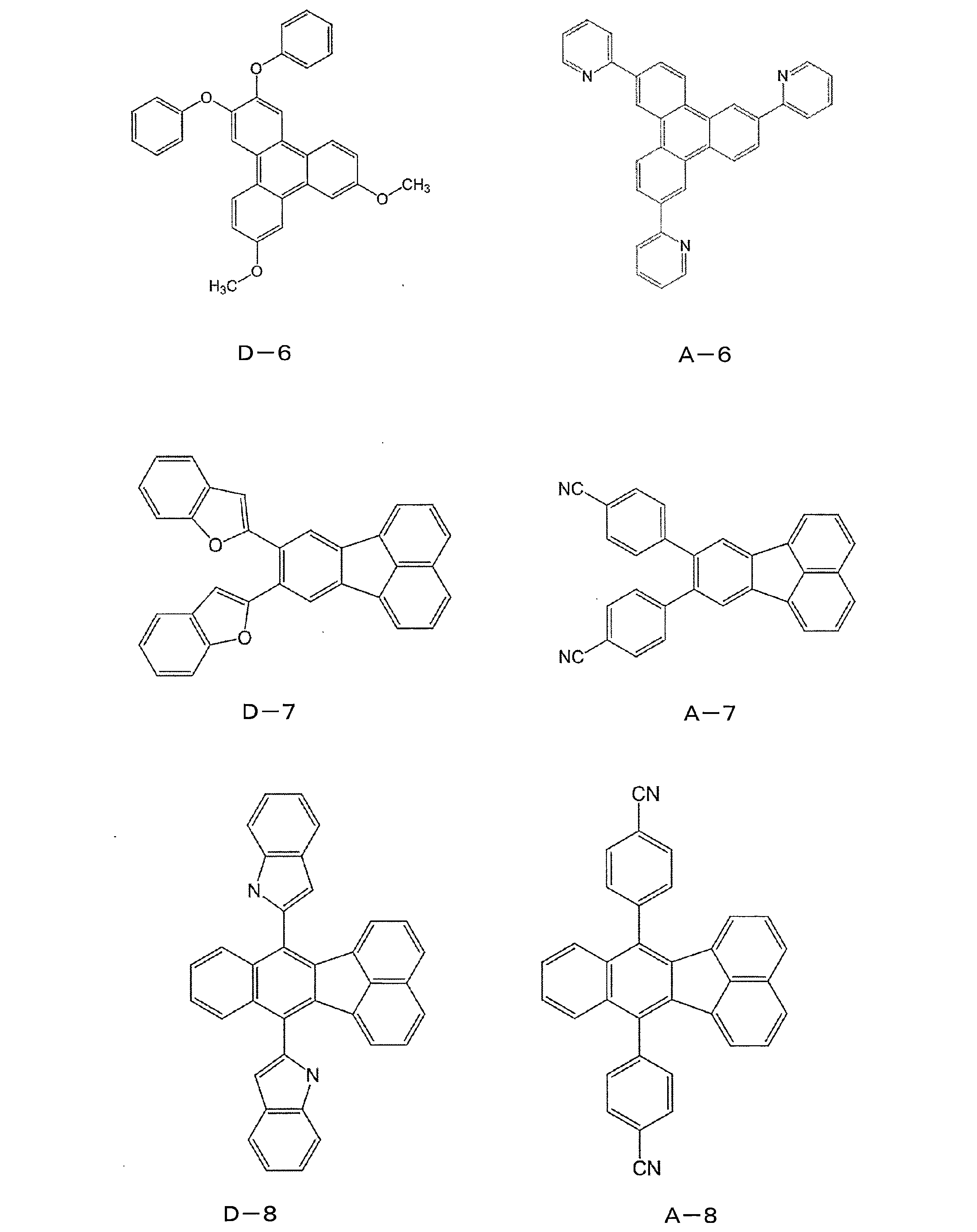
- This substrate is placed in a vacuum evaporation apparatus, and after evacuating until the degree of vacuum in the apparatus becomes 5 ⁇ 10 ⁇ 5 Pa or less, compound D-1 which is a p-type semiconductor material and an n-type semiconductor are used as a photoelectric conversion layer.
- Compound A-1 as a material was co-deposited at a deposition rate ratio of 1: 1 at 70 nm.
- 60 nm of aluminum was vapor-deposited to make an anode, and a 2 ⁇ 2 mm square photoelectric conversion element was produced.
- the film thickness referred to here is a crystal oscillation type film thickness monitor display value.
- a quartz substrate was placed in the same chamber simultaneously with the deposition of the photoelectric conversion layer to produce a 70 nm thin film.
- the spectral sensitivity characteristics, photocurrent value, and dark current value when a bias voltage (-3 V) was applied to the photoelectric conversion element were as follows.
- the ON / OFF ratio here means (photocurrent value at maximum sensitivity wavelength) / (dark current value).
- Maximum sensitivity wavelength 460 nm
- External quantum efficiency at maximum sensitivity wavelength 40%.
- Photocurrent value at maximum sensitivity wavelength 5.0 ⁇ 10 ⁇ 4 A / cm 2
- Dark current value 4.9 ⁇ 10 ⁇ 6 A / cm 2 ON / OFF ratio: 101
- Examples 2 to 11 Photoelectric conversion was performed in the same manner as in Example 1 except that the photoelectric conversion layer was vapor-deposited with a combination of the p-type semiconductor material and the n-type semiconductor material shown in Table 1 instead of Compound D-1 and Compound A-1. An element was produced. The results are shown in Tables 1-2.
- Comparative Examples 1 to 3 Except for depositing any one of compounds D-12, D-13, and D-14 having a skeleton different from that of compound A-1 instead of compound D-1 when depositing the photoelectric conversion layer, Examples In the same manner as in Example 1, a photoelectric conversion element was produced. The results are shown in Tables 1-2. Since the full width at half maximum at the maximum absorption wavelength was larger than that in Example 1, the device had poor color selectivity. Further, the balance between the hole transport property and the electron transport property was lost, and the external quantum efficiency at the maximum sensitivity wavelength was lowered as compared with Example 1. Furthermore, since the dark current value was larger than that in Example 1, the ON / OFF ratio was lowered.
- Comparative Example 4 A photoelectric conversion element was produced in the same manner as in Example 1 except that, when the photoelectric conversion layer was deposited, instead of the compound A-1, a compound A-15 having a skeleton different from that of the compound D-1 was deposited. .
- the results are shown in Tables 1-2. Although the external quantum efficiency at the maximum sensitivity wavelength was improved, the full width at half maximum at the maximum absorption wavelength was larger than that of the example, so that the device had poor color selectivity. In addition, the ON / OFF ratio was lower than that in Example 1.
- Comparative Example 5 A photoelectric conversion element was produced in the same manner as in Example 1 except that, when the photoelectric conversion layer was deposited, instead of compound D-1, compound A-16 having a skeleton different from that of compound A-1 was deposited. .
- the results are shown in Tables 1-2. Since the full width at half maximum at the maximum absorption wavelength was larger than that in Example 1, the device had poor color selectivity. Further, the balance between the hole transport property and the electron transport property was lost, and the external quantum efficiency at the maximum sensitivity wavelength was lowered as compared with Example 1. Furthermore, since the dark current value was larger than that in Example 1, the ON / OFF ratio was lowered.
- Comparative Examples 6 and 7 A photoelectric conversion element was produced in the same manner as in Example 1 except that only one of the compound D-1 and the compound A-1 was deposited when the photoelectric conversion layer was deposited. The results are shown in Tables 1-2. The external quantum efficiency at the maximum sensitivity wavelength was lower than that in Example 1. Furthermore, since the dark current value was larger than that in Example 1, the ON / OFF ratio was lowered.
- the photoelectric conversion element of the present invention can be applied to fields such as image sensors and solar cells.
- an image pickup element mounted on a mobile phone, a smartphone, a tablet personal computer, a digital still camera, or a photovoltaic device. It can be used in fields such as generators and sensing devices such as visible light sensors.
Landscapes
- Chemical & Material Sciences (AREA)
- Organic Chemistry (AREA)
- Physics & Mathematics (AREA)
- Materials Engineering (AREA)
- Spectroscopy & Molecular Physics (AREA)
- Engineering & Computer Science (AREA)
- Electromagnetism (AREA)
- Light Receiving Elements (AREA)
- Solid State Image Pick-Up Elements (AREA)
- Furan Compounds (AREA)
- Pyridine Compounds (AREA)
- Indole Compounds (AREA)
- Organic Low-Molecular-Weight Compounds And Preparation Thereof (AREA)
Abstract
Description
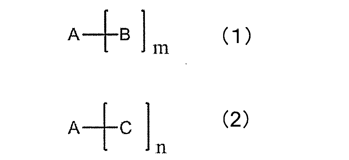
Bはアルコキシ基、アルキルチオ基、アリールエーテル基、アリールチオエーテル基、アミノ基、フラニル基、チオフェニル基、ピロリル基、ベンゾフラニル基、ベンゾチオフェニル基、インドリル基、ジベンゾフラニル基、ジベンゾチオフェニル基およびカルバゾリル基からなる群より選ばれる基であり、
Cは電子受容性窒素を含む芳香族複素環基であるか、もしくはアルキル基、シクロアルキル基、アルケニル基、シクロアルケニル基、アルキニル基、アリール基およびヘテロアリール基からなる群より選ばれる基であってハロゲンまたはシアノ基で置換されたものであり、
mおよびnはそれぞれ1~4の整数を表す。
ただし、一般式(1)においては、R1~R8、およびR1~R8のうち任意の隣接した基が互いに結合して形成した単環または縮合環、のいずれかm個の位置においてBと連結し、一般式(2)においては、R1~R8、およびR1~R8のうち任意の隣接した基が互いに結合して形成した単環または縮合環、のいずれかn個の位置においてCと連結する。
また、一般式(1)におけるAと一般式(2)におけるAは同一の基である。)
本発明の光電変換素子は、第一電極と第二電極の間に少なくとも一層の有機層が存在し、光を電気エネルギーに変換する光電変換素子であって、その有機層に後述の一般式(1)で表される化合物と一般式(2)で表される化合物を含有するものである。
本発明における一般式(1)および一般式(2)で表される化合物について詳細を説明する。
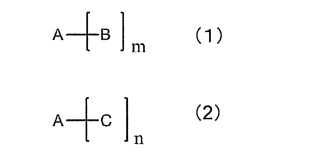
Bはアルコキシ基、アルキルチオ基、アリールエーテル基、アリールチオエーテル基、アミノ基、フラニル基、チオフェニル基、ピロリル基、ベンゾフラニル基、ベンゾチオフェニル基、インドリル基、ジベンゾフラニル基、ジベンゾチオフェニル基およびカルバゾリル基からなる群より選ばれる基であり、
Cは電子受容性窒素を含む芳香族複素環基であるか、もしくはアルキル基、シクロアルキル基、アルケニル基、シクロアルケニル基、アルキニル基、アリール基およびヘテロアリール基からなる群より選ばれる基であってハロゲンまたはシアノ基で置換されたものであり、
mおよびnはそれぞれ1~4の整数を表す。

ただし、一般式(1)においては、R1~R8、およびR1~R8のうち任意の隣接した基が互いに結合して形成した単環または縮合環、のいずれかm個の位置においてBと連結し、一般式(2)においては、R1~R8、およびR1~R8のうち任意の隣接した基が互いに結合して形成した単環または縮合環、のいずれかn個の位置においてCと連結する。
また、一般式(1)におけるAと一般式(2)におけるAは同一の基である。

光電変換層とは入射光を吸収して電荷を発生する光電変換が生じる層である。これは単独の光電変換材料で構成されても良いが、p型半導体材料とn型半導体材料とで構成されることが好ましい。この際、p型半導体材料とn型半導体材料はそれぞれ単独でも複数でもよい。光電変換層では光電変換材料が光を吸収し、励起子を形成した後、電子と正孔がそれぞれn型半導体材料とp型半導体材料により、分離される。このように分離された電子と正孔はそれぞれ伝導準位と価電子準位を通して両極まで流され、電気エネルギーを発生させる。
本発明の光電変換素子において、陰極と陽極は素子の中で作られた電子及び正孔を流し、十分に電流を流せるための役割を有するものである。これらは、光を光電変換層に入らせるために、少なくとも一方は透明または半透明であることが望ましい。通常、基板上に形成される陰極を透明電極とすることが好ましい。
電荷阻止層とは、光電変換層で光電変換された電子および正孔を効率よくかつ安定に電極から取り出すために用いられる層であり、電子を阻止する電子阻止層と正孔を阻止する正孔阻止層とが挙げられる。これらは無機物から構成されても良いし、有機化合物から構成されても良い。さらに、無機物と有機化合物の混合層からなってもよい。
本発明の光電変換素子はイメージセンサに好適に利用できる。イメージセンサは光学的な映像を電気的な信号に変換する半導体素子である。一般的にイメージセンサは光を電気エネルギーに変換する前述の光電変換素子と電気エネルギーを電気信号に読み出す回路で構成される。イメージセンサの用途によって、複数の光電変換素子を一次元直線または二次元平面に配列することができる。
ともに同一骨格を有する化合物D-1および化合物A-1を用いた光電変換素子を次のように作製した。
最大吸収波長:471nm
最大吸収波長における半値幅:98nm
最大吸収波長における吸収係数:6.41×10⁴/cm。
最大感度波長:460nm
最大感度波長における外部量子効率:40%。
最大感度波長における光電流値:5.0×10⁻⁴A/cm2
暗電流値:4.9×10⁻⁶A/cm2
ON/OFF比:101

光電変換層を蒸着する時、化合物D-1、化合物A-1のかわりに、表1に示すp型半導体材料およびn型半導体材料の組み合わせで蒸着した以外は、実施例1と同様に光電変換素子を作製した。結果を表1~2に示す。



光電変換層を蒸着する時、化合物D-1のかわりに、化合物A-1とは異なる骨格を有する化合物D-12、D-13、D-14のいずれかを蒸着したこと以外は、実施例1と同様にして光電変換素子を作製した。結果を表1~2に示す。最大吸収波長における半値幅が実施例1と比べ大きくなったので、色選択性の悪い素子となった。また、正孔輸送性と電子輸送性のバランスが崩れ、実施例1と比べ最大感度波長における外部量子効率が低下した。さらに、暗電流値が実施例1と比べて大きくなったので、ON/OFF比が低下した。

光電変換層を蒸着する時、化合物A-1のかわりに、化合物D-1とは異なる骨格を有する化合物A-15を蒸着したこと以外は、実施例1と同様にして光電変換素子を作製した。結果を表1~2に示す。最大感度波長における外部量子効率は向上したものの、最大吸収波長における半値幅が実施例と比べ大きくなったので、色選択性の悪い素子となった。また、実施例1と比べON/OFF比が低下した。

光電変換層を蒸着する時、化合物D-1のかわりに、化合物A-1とは異なる骨格を有する化合物A-16を蒸着したこと以外は、実施例1と同様にして光電変換素子を作製した。結果を表1~2に示す。最大吸収波長における半値幅が実施例1と比べ大きくなったので、色選択性の悪い素子となった。また、正孔輸送性と電子輸送性のバランスが崩れ、実施例1と比べ最大感度波長における外部量子効率が低下した。さらに、暗電流値が実施例1と比べて大きくなったので、ON/OFF比が低下した。
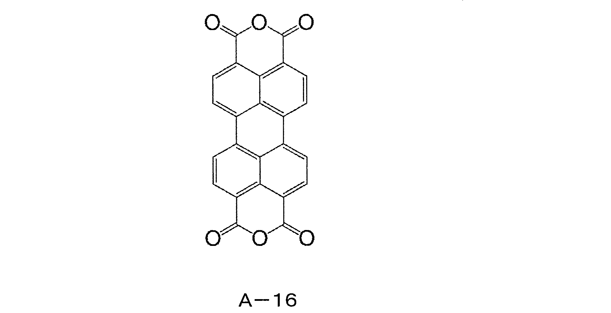
光電変換層を蒸着する時、化合物D-1および化合物A-1のいずれか一方のみを蒸着したこと以外は、実施例1と同様にして光電変換素子を作製した。結果を表1~2に示す。最大感度波長における外部量子効率が実施例1と比べて低下した。さらに、暗電流値が実施例1と比べて大きくなったので、ON/OFF比が低下した。


13 電子阻止層
15 有機層
17 正孔阻止層
20 第二電極
31 一般式(1)で表される化合物の分子
32 一般式(2)で表される化合物の分子
33 特定骨格を有する化合物の分子
34 化合物分子33とは異なる骨格を有する化合物の分子
41 赤色光を検出する光電変換素子
42 緑色光を検出する光電変換素子
43 青色光を検出する光電変換素子
Claims (15)
- 第一電極と第二電極の間に少なくとも一層の有機層が存在する光電変換素子であって、前記有機層に一般式(1)で表される化合物と一般式(2)で表される化合物とを含有することを特徴とする光電変換素子。

Bはアルコキシ基、アルキルチオ基、アリールエーテル基、アリールチオエーテル基、アミノ基、フラニル基、チオフェニル基、ピロリル基、ベンゾフラニル基、ベンゾチオフェニル基、インドリル基、ジベンゾフラニル基、ジベンゾチオフェニル基およびカルバゾリル基からなる群より選ばれる基であり、
Cは電子受容性窒素を含む芳香族複素環基であるか、もしくはアルキル基、シクロアルキル基、アルケニル基、シクロアルケニル基、アルキニル基、アリール基およびヘテロアリール基からなる群より選ばれる基であってハロゲンまたはシアノ基で置換されたものであり、
mおよびnはそれぞれ1~4の整数を表す。
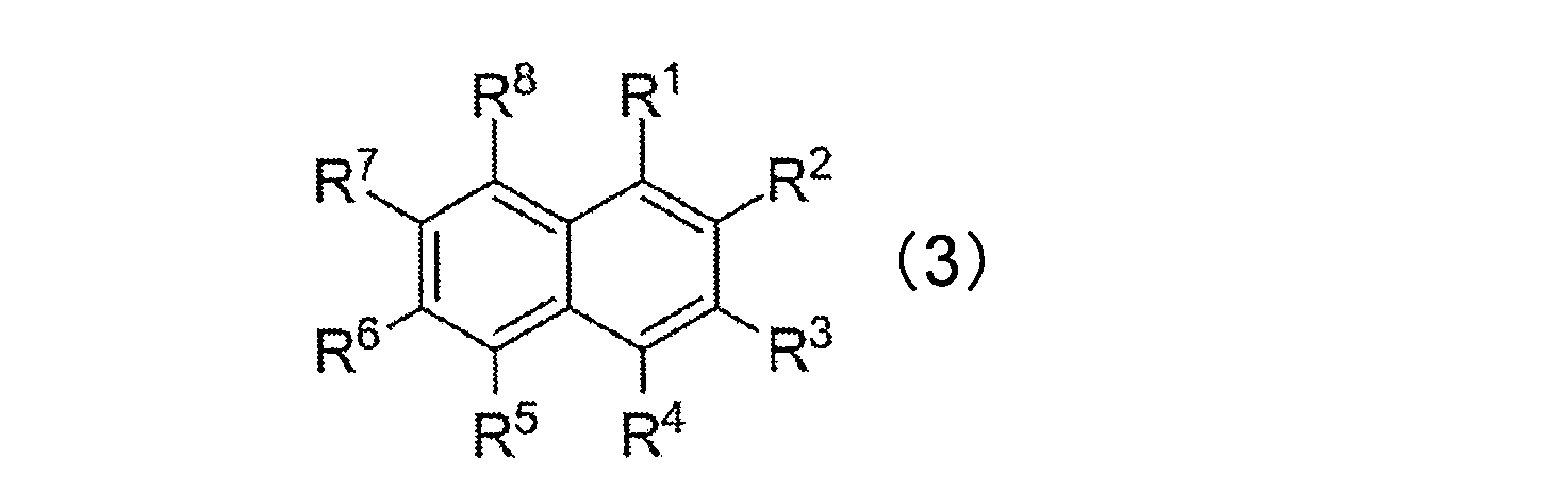
ただし、一般式(1)においてはR1~R8およびR1~R8のうち任意の隣接した基が互いに結合して形成した縮合環、のいずれかm個の位置においてBと連結し、一般式(2)においてはR1~R8およびR1~R8のうち任意の隣接した基が互いに結合して形成した縮合環、のいずれかn個の位置においてCと連結する。
また、一般式(1)におけるAと一般式(2)におけるAは同一の基である。) - 一般式(3)のR1~R8において隣接する基が互いに結合し、全体で3~6環からなる縮合環を形成することを特徴とする請求項1記載の光電変換素子。
- 一般式(3)がアントラセン、フェナンスレン、ナフタセン、ピレン、クリセン、トリフェニレン、フルオランテン、ベンゾフルオランテン、ペリレン、ペンタセン、ヘキサセンの中から選ばれる環構造である請求項2記載の光電変換素子。
- 一般式(1)で表される化合物のイオン化ポテンシャル(Ip1)と電子親和力(Ea1)、および一般式(2)で表される化合物のイオン化ポテンシャル(Ip2)と電子親和力(Ea2)が、Ip1<Ip2かつEa1<Ea2である請求項1~3のいずれか記載の光電変換素子。
- 一般式(1)で表される化合物の吸収スペクトルの極大値と、一般式(2)で表される化合物の吸収スペクトルの極大値との差が50nm以下である請求項1~4いずれか記載の光電変換素子。
- 一般式(1)で表される化合物の吸収スペクトルの半値幅と、一般式(2)で表される化合物の吸収スペクトルの半値幅が、いずれも25nm以上100nm以下である請求項1~5いずれか記載の光電変換素子。
- 前記有機層が複数層で構成され、それらのうちの一層に一般式(1)で表される化合物と一般式(2)で表される化合物の両方が含まれる請求項1~6のいずれか記載の光電変換素子。
- 前記有機層のうち一般式(1)で表される化合物と一般式(2)で表される化合物の両方が含まれる層が、それらによるバルクヘテロ接合層であることを特徴とする請求項7記載の光電変換素子。
- 一般式(1)で表される化合物と上記一般式(2)で表される化合物の混合比が1:3乃至3:1である請求項7または8記載の光電変換素子。
- 前記有機層の膜厚が20nm以上200nm以下である請求項1~9のいずれか記載の光電変換素子。
- さらに、前記有機層に電界を印加する電圧印加部を備えた請求項1~10のいずれか記載の光電変換素子。
- 前記電圧印加部は、前記有機層に105V/m以上109V/m以下の電界を印加するものである請求項1~11のいずれか記載の光電変換素子。
- 請求項1~12いずれか記載の光電変換素子を含むイメージセンサ。
- 2種類以上の光電変換素子で構成され、そのうちの少なくとも1種類の光電変換素子が請求項1~12いずれか記載の光電変換素子である請求項13記載のイメージセンサ。
- 前記2種類以上の光電変換素子が積層構造を有し、そのうちの少なくとも1種類の光電変換素子が請求項1~12いずれか記載の光電変換素子である請求項14記載のイメージセンサ。
Priority Applications (4)
| Application Number | Priority Date | Filing Date | Title |
|---|---|---|---|
| JP2015562230A JP5988001B1 (ja) | 2015-01-09 | 2015-12-18 | 光電変換素子およびこれを用いたイメージセンサ |
| US15/534,768 US10199589B2 (en) | 2015-01-09 | 2015-12-18 | Photoelectric conversion element and image sensor using same |
| KR1020177017528A KR102190596B1 (ko) | 2015-01-09 | 2015-12-18 | 광전 변환 소자 및 이것을 사용한 이미지 센서 |
| CN201580072492.8A CN107112380B (zh) | 2015-01-09 | 2015-12-18 | 光电转换元件及使用其的图像传感器 |
Applications Claiming Priority (2)
| Application Number | Priority Date | Filing Date | Title |
|---|---|---|---|
| JP2015-002862 | 2015-01-09 | ||
| JP2015002862 | 2015-01-09 |
Publications (1)
| Publication Number | Publication Date |
|---|---|
| WO2016111140A1 true WO2016111140A1 (ja) | 2016-07-14 |
Family
ID=56355842
Family Applications (1)
| Application Number | Title | Priority Date | Filing Date |
|---|---|---|---|
| PCT/JP2015/085503 Ceased WO2016111140A1 (ja) | 2015-01-09 | 2015-12-18 | 光電変換素子およびこれを用いたイメージセンサ |
Country Status (6)
| Country | Link |
|---|---|
| US (1) | US10199589B2 (ja) |
| JP (1) | JP5988001B1 (ja) |
| KR (1) | KR102190596B1 (ja) |
| CN (1) | CN107112380B (ja) |
| TW (1) | TWI683463B (ja) |
| WO (1) | WO2016111140A1 (ja) |
Cited By (3)
| Publication number | Priority date | Publication date | Assignee | Title |
|---|---|---|---|---|
| JP2022175575A (ja) * | 2021-05-14 | 2022-11-25 | 日本化薬株式会社 | 有機半導体材料及びその用途 |
| US11557741B2 (en) | 2018-11-14 | 2023-01-17 | Samsung Electronics Co., Ltd. | Photoelectric conversion devices and organic sensors and electronic devices |
| KR20230113324A (ko) | 2020-11-27 | 2023-07-28 | 닛테츠 케미컬 앤드 머티리얼 가부시키가이샤 | 촬상용 광전 변환 소자용 재료 |
Families Citing this family (6)
| Publication number | Priority date | Publication date | Assignee | Title |
|---|---|---|---|---|
| CN108039422B (zh) * | 2017-12-19 | 2019-07-09 | 天津大学 | 应用于溶液加工型有机电致发光器件的电子传输材料及制备方法 |
| JP2019186500A (ja) * | 2018-04-17 | 2019-10-24 | ソニー株式会社 | 光電変換素子および撮像装置 |
| CN109651346A (zh) * | 2018-12-31 | 2019-04-19 | 瑞声科技(南京)有限公司 | 一种萘基杂环化合物及其应用 |
| CN110386895B (zh) * | 2019-07-19 | 2022-11-01 | 河南省科学院化学研究所有限公司 | 一种合成n-乙烯基咔唑的方法 |
| CN112694394B (zh) * | 2020-08-25 | 2022-05-27 | 天津大学 | 超灵敏多输出信号生物传感器及其制备方法和应用 |
| CN114773169B (zh) * | 2022-04-21 | 2023-12-19 | 湖南大学 | peri-位化学修饰的苝衍生物功能分子及其制备和应用 |
Citations (3)
| Publication number | Priority date | Publication date | Assignee | Title |
|---|---|---|---|---|
| JP2007335760A (ja) * | 2006-06-16 | 2007-12-27 | Fujifilm Corp | 光電変換膜、並びに、該光電変換膜を含む太陽電池、光電変換素子、又は撮像素子 |
| JP2011009622A (ja) * | 2009-06-29 | 2011-01-13 | Asahi Kasei Corp | 有機薄膜太陽電池用薄膜の製造方法 |
| JP2012519382A (ja) * | 2009-03-05 | 2012-08-23 | コモンウェルス サイエンティフィック アンド インダストリアル リサーチ オーガニゼイション | 多環式芳香族化合物を含有する感光性光電子デバイス |
Family Cites Families (14)
| Publication number | Priority date | Publication date | Assignee | Title |
|---|---|---|---|---|
| JPH05129576A (ja) | 1991-11-06 | 1993-05-25 | Mitsubishi Kasei Corp | 画像読み取り素子 |
| JP3423279B2 (ja) | 2000-09-01 | 2003-07-07 | 科学技術振興事業団 | 有機半導体薄膜太陽電池 |
| EP1730795A2 (en) * | 2004-03-31 | 2006-12-13 | Matsushita Electric Industrial Co., Ltd. | Organic photoelectric conversion element utilizing an inorganic buffer layer placed between an electrode and the active material |
| JP2006100766A (ja) * | 2004-08-31 | 2006-04-13 | Fuji Photo Film Co Ltd | 光電変換素子、及び撮像素子、並びに、これらに電場を印加する方法。 |
| KR101378047B1 (ko) * | 2006-06-15 | 2014-03-27 | 도레이 카부시키가이샤 | 발광소자재료 및 발광소자 |
| KR20090123540A (ko) | 2008-05-28 | 2009-12-02 | 삼성전자주식회사 | 유기 광전 변환막, 이를 구비하는 광전 변환 소자 및이미지 센서 |
| JP2010034494A (ja) | 2008-06-30 | 2010-02-12 | Sumitomo Chemical Co Ltd | 有機光電変換素子 |
| JP5520560B2 (ja) | 2009-09-29 | 2014-06-11 | 富士フイルム株式会社 | 光電変換素子、光電変換素子材料、光センサ、及び撮像素子 |
| WO2012017842A1 (en) * | 2010-08-02 | 2012-02-09 | Semiconductor Energy Laboratory Co., Ltd. | Triazole derivative, heterocyclic compound, light-emitting element, light-emitting device, electronic device and lighting device |
| KR101996649B1 (ko) * | 2011-04-15 | 2019-07-04 | 에스에프씨 주식회사 | 피렌 유도체 화합물 및 이를 포함하는 유기전계발광소자 |
| KR102069891B1 (ko) * | 2011-08-31 | 2020-01-28 | 삼성전자주식회사 | 광전 변환 소자 |
| CN103814453B (zh) * | 2011-09-16 | 2016-12-28 | 东丽株式会社 | 发光元件材料及发光元件 |
| JP2015013804A (ja) * | 2011-09-16 | 2015-01-22 | 出光興産株式会社 | 芳香族アミン誘導体およびそれを用いた有機エレクトロルミネッセンス素子 |
| US9508945B2 (en) * | 2012-06-27 | 2016-11-29 | Regents Of The University Of Minnesota | Spectrally tunable broadband organic photodetectors |
-
2015
- 2015-12-18 WO PCT/JP2015/085503 patent/WO2016111140A1/ja not_active Ceased
- 2015-12-18 KR KR1020177017528A patent/KR102190596B1/ko active Active
- 2015-12-18 JP JP2015562230A patent/JP5988001B1/ja active Active
- 2015-12-18 CN CN201580072492.8A patent/CN107112380B/zh active Active
- 2015-12-18 US US15/534,768 patent/US10199589B2/en active Active
-
2016
- 2016-01-06 TW TW105100215A patent/TWI683463B/zh not_active IP Right Cessation
Patent Citations (3)
| Publication number | Priority date | Publication date | Assignee | Title |
|---|---|---|---|---|
| JP2007335760A (ja) * | 2006-06-16 | 2007-12-27 | Fujifilm Corp | 光電変換膜、並びに、該光電変換膜を含む太陽電池、光電変換素子、又は撮像素子 |
| JP2012519382A (ja) * | 2009-03-05 | 2012-08-23 | コモンウェルス サイエンティフィック アンド インダストリアル リサーチ オーガニゼイション | 多環式芳香族化合物を含有する感光性光電子デバイス |
| JP2011009622A (ja) * | 2009-06-29 | 2011-01-13 | Asahi Kasei Corp | 有機薄膜太陽電池用薄膜の製造方法 |
Cited By (5)
| Publication number | Priority date | Publication date | Assignee | Title |
|---|---|---|---|---|
| US11557741B2 (en) | 2018-11-14 | 2023-01-17 | Samsung Electronics Co., Ltd. | Photoelectric conversion devices and organic sensors and electronic devices |
| KR20230113324A (ko) | 2020-11-27 | 2023-07-28 | 닛테츠 케미컬 앤드 머티리얼 가부시키가이샤 | 촬상용 광전 변환 소자용 재료 |
| US12426503B2 (en) | 2020-11-27 | 2025-09-23 | Nippon Steel Chemical & Material Co., Ltd. | Material for photoelectric conversion element for imaging |
| JP2022175575A (ja) * | 2021-05-14 | 2022-11-25 | 日本化薬株式会社 | 有機半導体材料及びその用途 |
| JP7741493B2 (ja) | 2021-05-14 | 2025-09-18 | 日本化薬株式会社 | 有機半導体材料及びその用途 |
Also Published As
| Publication number | Publication date |
|---|---|
| CN107112380A (zh) | 2017-08-29 |
| KR20170104999A (ko) | 2017-09-18 |
| US10199589B2 (en) | 2019-02-05 |
| US20170309849A1 (en) | 2017-10-26 |
| TW201631815A (zh) | 2016-09-01 |
| JPWO2016111140A1 (ja) | 2017-04-27 |
| TWI683463B (zh) | 2020-01-21 |
| JP5988001B1 (ja) | 2016-09-07 |
| CN107112380B (zh) | 2019-06-21 |
| KR102190596B1 (ko) | 2020-12-14 |
Similar Documents
| Publication | Publication Date | Title |
|---|---|---|
| JP5988001B1 (ja) | 光電変換素子およびこれを用いたイメージセンサ | |
| EP3961737B1 (en) | Composition for photoelectric device, and image sensor and electronic device including the same | |
| EP3026722B1 (en) | Compound for organic photoelectric device and organic photoelectric device, image sensor, and electronic device including the same | |
| KR102480671B1 (ko) | 광전 변환 소자 및 이미지 센서 | |
| JP6610257B2 (ja) | 光電変換素子ならびにそれを用いたイメージセンサ、太陽電池、単色検知センサおよびフレキシブルセンサ | |
| EP3228623A1 (en) | Compound and organic photoelectric device, image sensor and electronic device including the same | |
| CN113105458A (zh) | 化合物以及包括其的光电器件、图像传感器、和电子设备 | |
| US9997718B2 (en) | Organic photoelectric device image sensor and electronic device | |
| CN105712993A (zh) | 用于有机光电器件的化合物以及包括其的有机光电器件、图像传感器和电子器件 | |
| JP2016152239A (ja) | 光電変換素子およびそれを用いたイメージセンサ | |
| EP4024484B1 (en) | Composition for photoelectric device, and photoelectric device, image sensor, and electronic device including the same | |
| KR102798537B1 (ko) | 화합물, 및 이를 포함하는 광전 소자, 이미지 센서 및 전자 장치 | |
| JP2016072547A (ja) | 光電変換素子およびこれを用いたイメージセンサ | |
| KR20220096214A (ko) | 청색 흡수용 필름, 광전 소자 및 이를 포함하는 이미지 센서와 전자 장치 | |
| JP7572830B2 (ja) | 化合物及びこれを含む光電素子並びにイメージセンサー及び電子装置 | |
| EP4458829A1 (en) | 4h,8h-thieno[3',2':5,6]pyrido[3,2,1-de]acridine derivatives derivatives with high extinction coefficients for use as materials in photoelectronic devices and image sensors | |
| JP2016100551A (ja) | 光電変換素子およびこれを用いたイメージセンサ |
Legal Events
| Date | Code | Title | Description |
|---|---|---|---|
| ENP | Entry into the national phase |
Ref document number: 2015562230 Country of ref document: JP Kind code of ref document: A |
|
| 121 | Ep: the epo has been informed by wipo that ep was designated in this application |
Ref document number: 15877013 Country of ref document: EP Kind code of ref document: A1 |
|
| WWE | Wipo information: entry into national phase |
Ref document number: 15534768 Country of ref document: US |
|
| ENP | Entry into the national phase |
Ref document number: 20177017528 Country of ref document: KR Kind code of ref document: A |
|
| NENP | Non-entry into the national phase |
Ref country code: DE |
|
| 122 | Ep: pct application non-entry in european phase |
Ref document number: 15877013 Country of ref document: EP Kind code of ref document: A1 |