WO2016110892A1 - 太陽電池用fzシリコン単結晶の製造方法及び太陽電池 - Google Patents
太陽電池用fzシリコン単結晶の製造方法及び太陽電池 Download PDFInfo
- Publication number
- WO2016110892A1 WO2016110892A1 PCT/JP2015/005860 JP2015005860W WO2016110892A1 WO 2016110892 A1 WO2016110892 A1 WO 2016110892A1 JP 2015005860 W JP2015005860 W JP 2015005860W WO 2016110892 A1 WO2016110892 A1 WO 2016110892A1
- Authority
- WO
- WIPO (PCT)
- Prior art keywords
- silicon single
- single crystal
- gallium
- solar cell
- producing
- Prior art date
- Legal status (The legal status is an assumption and is not a legal conclusion. Google has not performed a legal analysis and makes no representation as to the accuracy of the status listed.)
- Ceased
Links
Images

Classifications
-
- C—CHEMISTRY; METALLURGY
- C30—CRYSTAL GROWTH
- C30B—SINGLE-CRYSTAL GROWTH; UNIDIRECTIONAL SOLIDIFICATION OF EUTECTIC MATERIAL OR UNIDIRECTIONAL DEMIXING OF EUTECTOID MATERIAL; REFINING BY ZONE-MELTING OF MATERIAL; PRODUCTION OF A HOMOGENEOUS POLYCRYSTALLINE MATERIAL WITH DEFINED STRUCTURE; SINGLE CRYSTALS OR HOMOGENEOUS POLYCRYSTALLINE MATERIAL WITH DEFINED STRUCTURE; AFTER-TREATMENT OF SINGLE CRYSTALS OR A HOMOGENEOUS POLYCRYSTALLINE MATERIAL WITH DEFINED STRUCTURE; APPARATUS THEREFOR
- C30B13/00—Single-crystal growth by zone-melting; Refining by zone-melting
- C30B13/08—Single-crystal growth by zone-melting; Refining by zone-melting adding crystallising materials or reactants forming it in situ to the molten zone
- C30B13/10—Single-crystal growth by zone-melting; Refining by zone-melting adding crystallising materials or reactants forming it in situ to the molten zone with addition of doping materials
- C30B13/12—Single-crystal growth by zone-melting; Refining by zone-melting adding crystallising materials or reactants forming it in situ to the molten zone with addition of doping materials in the gaseous or vapour state
-
- C—CHEMISTRY; METALLURGY
- C30—CRYSTAL GROWTH
- C30B—SINGLE-CRYSTAL GROWTH; UNIDIRECTIONAL SOLIDIFICATION OF EUTECTIC MATERIAL OR UNIDIRECTIONAL DEMIXING OF EUTECTOID MATERIAL; REFINING BY ZONE-MELTING OF MATERIAL; PRODUCTION OF A HOMOGENEOUS POLYCRYSTALLINE MATERIAL WITH DEFINED STRUCTURE; SINGLE CRYSTALS OR HOMOGENEOUS POLYCRYSTALLINE MATERIAL WITH DEFINED STRUCTURE; AFTER-TREATMENT OF SINGLE CRYSTALS OR A HOMOGENEOUS POLYCRYSTALLINE MATERIAL WITH DEFINED STRUCTURE; APPARATUS THEREFOR
- C30B13/00—Single-crystal growth by zone-melting; Refining by zone-melting
-
- C—CHEMISTRY; METALLURGY
- C30—CRYSTAL GROWTH
- C30B—SINGLE-CRYSTAL GROWTH; UNIDIRECTIONAL SOLIDIFICATION OF EUTECTIC MATERIAL OR UNIDIRECTIONAL DEMIXING OF EUTECTOID MATERIAL; REFINING BY ZONE-MELTING OF MATERIAL; PRODUCTION OF A HOMOGENEOUS POLYCRYSTALLINE MATERIAL WITH DEFINED STRUCTURE; SINGLE CRYSTALS OR HOMOGENEOUS POLYCRYSTALLINE MATERIAL WITH DEFINED STRUCTURE; AFTER-TREATMENT OF SINGLE CRYSTALS OR A HOMOGENEOUS POLYCRYSTALLINE MATERIAL WITH DEFINED STRUCTURE; APPARATUS THEREFOR
- C30B15/00—Single-crystal growth by pulling from a melt, e.g. Czochralski method
-
- C—CHEMISTRY; METALLURGY
- C30—CRYSTAL GROWTH
- C30B—SINGLE-CRYSTAL GROWTH; UNIDIRECTIONAL SOLIDIFICATION OF EUTECTIC MATERIAL OR UNIDIRECTIONAL DEMIXING OF EUTECTOID MATERIAL; REFINING BY ZONE-MELTING OF MATERIAL; PRODUCTION OF A HOMOGENEOUS POLYCRYSTALLINE MATERIAL WITH DEFINED STRUCTURE; SINGLE CRYSTALS OR HOMOGENEOUS POLYCRYSTALLINE MATERIAL WITH DEFINED STRUCTURE; AFTER-TREATMENT OF SINGLE CRYSTALS OR A HOMOGENEOUS POLYCRYSTALLINE MATERIAL WITH DEFINED STRUCTURE; APPARATUS THEREFOR
- C30B15/00—Single-crystal growth by pulling from a melt, e.g. Czochralski method
- C30B15/02—Single-crystal growth by pulling from a melt, e.g. Czochralski method adding crystallising materials or reactants forming it in situ to the melt
- C30B15/04—Single-crystal growth by pulling from a melt, e.g. Czochralski method adding crystallising materials or reactants forming it in situ to the melt adding doping materials, e.g. for n-p-junction
-
- C—CHEMISTRY; METALLURGY
- C30—CRYSTAL GROWTH
- C30B—SINGLE-CRYSTAL GROWTH; UNIDIRECTIONAL SOLIDIFICATION OF EUTECTIC MATERIAL OR UNIDIRECTIONAL DEMIXING OF EUTECTOID MATERIAL; REFINING BY ZONE-MELTING OF MATERIAL; PRODUCTION OF A HOMOGENEOUS POLYCRYSTALLINE MATERIAL WITH DEFINED STRUCTURE; SINGLE CRYSTALS OR HOMOGENEOUS POLYCRYSTALLINE MATERIAL WITH DEFINED STRUCTURE; AFTER-TREATMENT OF SINGLE CRYSTALS OR A HOMOGENEOUS POLYCRYSTALLINE MATERIAL WITH DEFINED STRUCTURE; APPARATUS THEREFOR
- C30B15/00—Single-crystal growth by pulling from a melt, e.g. Czochralski method
- C30B15/20—Controlling or regulating
-
- C—CHEMISTRY; METALLURGY
- C30—CRYSTAL GROWTH
- C30B—SINGLE-CRYSTAL GROWTH; UNIDIRECTIONAL SOLIDIFICATION OF EUTECTIC MATERIAL OR UNIDIRECTIONAL DEMIXING OF EUTECTOID MATERIAL; REFINING BY ZONE-MELTING OF MATERIAL; PRODUCTION OF A HOMOGENEOUS POLYCRYSTALLINE MATERIAL WITH DEFINED STRUCTURE; SINGLE CRYSTALS OR HOMOGENEOUS POLYCRYSTALLINE MATERIAL WITH DEFINED STRUCTURE; AFTER-TREATMENT OF SINGLE CRYSTALS OR A HOMOGENEOUS POLYCRYSTALLINE MATERIAL WITH DEFINED STRUCTURE; APPARATUS THEREFOR
- C30B29/00—Single crystals or homogeneous polycrystalline material with defined structure characterised by the material or by their shape
- C30B29/02—Elements
- C30B29/06—Silicon
-
- H—ELECTRICITY
- H10—SEMICONDUCTOR DEVICES; ELECTRIC SOLID-STATE DEVICES NOT OTHERWISE PROVIDED FOR
- H10F—INORGANIC SEMICONDUCTOR DEVICES SENSITIVE TO INFRARED RADIATION, LIGHT, ELECTROMAGNETIC RADIATION OF SHORTER WAVELENGTH OR CORPUSCULAR RADIATION
- H10F10/00—Individual photovoltaic cells, e.g. solar cells
- H10F10/10—Individual photovoltaic cells, e.g. solar cells having potential barriers
- H10F10/14—Photovoltaic cells having only PN homojunction potential barriers
-
- H—ELECTRICITY
- H10—SEMICONDUCTOR DEVICES; ELECTRIC SOLID-STATE DEVICES NOT OTHERWISE PROVIDED FOR
- H10F—INORGANIC SEMICONDUCTOR DEVICES SENSITIVE TO INFRARED RADIATION, LIGHT, ELECTROMAGNETIC RADIATION OF SHORTER WAVELENGTH OR CORPUSCULAR RADIATION
- H10F77/00—Constructional details of devices covered by this subclass
- H10F77/10—Semiconductor bodies
- H10F77/12—Active materials
- H10F77/122—Active materials comprising only Group IV materials
- H10F77/1223—Active materials comprising only Group IV materials characterised by the dopants
-
- Y—GENERAL TAGGING OF NEW TECHNOLOGICAL DEVELOPMENTS; GENERAL TAGGING OF CROSS-SECTIONAL TECHNOLOGIES SPANNING OVER SEVERAL SECTIONS OF THE IPC; TECHNICAL SUBJECTS COVERED BY FORMER USPC CROSS-REFERENCE ART COLLECTIONS [XRACs] AND DIGESTS
- Y02—TECHNOLOGIES OR APPLICATIONS FOR MITIGATION OR ADAPTATION AGAINST CLIMATE CHANGE
- Y02E—REDUCTION OF GREENHOUSE GAS [GHG] EMISSIONS, RELATED TO ENERGY GENERATION, TRANSMISSION OR DISTRIBUTION
- Y02E10/00—Energy generation through renewable energy sources
- Y02E10/50—Photovoltaic [PV] energy
-
- Y—GENERAL TAGGING OF NEW TECHNOLOGICAL DEVELOPMENTS; GENERAL TAGGING OF CROSS-SECTIONAL TECHNOLOGIES SPANNING OVER SEVERAL SECTIONS OF THE IPC; TECHNICAL SUBJECTS COVERED BY FORMER USPC CROSS-REFERENCE ART COLLECTIONS [XRACs] AND DIGESTS
- Y02—TECHNOLOGIES OR APPLICATIONS FOR MITIGATION OR ADAPTATION AGAINST CLIMATE CHANGE
- Y02E—REDUCTION OF GREENHOUSE GAS [GHG] EMISSIONS, RELATED TO ENERGY GENERATION, TRANSMISSION OR DISTRIBUTION
- Y02E10/00—Energy generation through renewable energy sources
- Y02E10/50—Photovoltaic [PV] energy
- Y02E10/547—Monocrystalline silicon PV cells
Definitions
- the present invention relates to a method for producing an FZ silicon single crystal for a solar cell, and a solar cell produced using the FZ silicon single crystal.
- the single-crystal silicon manufacturing method includes a CZ (Czochralsky) method in which high-purity polysilicon is melted in a quartz crucible, and a seed crystal is brought into contact with it to slowly grow and pull up, and part of a rod-like high-purity polysilicon. Is heated, and a molten part is formed between the lower single crystal serving as a seed crystal and a rod-shaped raw material crystal (polysilicon, etc.), and the whole is moved downward while supporting the melt part by surface tension.
- FZ Float Zone
- a silicon single crystal manufactured by the CZ method contains oxygen from a quartz crucible. If the concentration is high, a large number of oxygen defect nuclei are retained. On the other hand, the silicon crystal produced by the above FZ method has few oxygen defect nuclei because of its low oxygen content. Further, Patent Document 1 discloses that an FZ silicon single crystal is produced by the FZ method using a CZ silicon single crystal produced by the CZ method as a raw material rod, and the FZ silicon single crystal produced in this way is also disclosed. Patent Document 1 also discloses that the oxygen content is low.
- a p-type silicon substrate doped with gallium is used as a silicon substrate used in a solar cell in order to suppress a decrease in the lifetime of minority carriers (see, for example, Patent Document 2). .
- the present inventor manufactures a solar cell from an FZ silicon single crystal manufactured by the FZ method using a CZ silicon single crystal as a raw material rod, since the oxygen content in the silicon single crystal is small, oxygen defects are not easily generated. Unlike the case of manufacturing from CZ silicon crystal manufactured by the CZ method, the lifetime of minority carriers due to oxygen defects is suppressed even after going through the same process, and a solar cell with high conversion efficiency is manufactured. I found that it was possible. The present inventor further paid attention to improving the minority carrier lifetime by using a p-type silicon substrate doped with gallium, and developed a CZ silicon single crystal in which a silicon single crystal for solar cells was doped with gallium. It tried to manufacture by FZ method using it as a raw material stick.
- gallium-doped FZ silicon single crystal when an attempt is made to produce a gallium-doped FZ silicon single crystal by the FZ method using a gallium-doped CZ silicon single crystal as a raw material rod, the gallium as a dopant evaporates when the float zone of the raw material rod is melted. In addition, only a high resistance gallium-doped FZ silicon single crystal can be obtained. When a solar cell is manufactured using such a silicon single crystal, there is a problem that the internal resistance becomes too high and the conversion efficiency is lowered.
- An object of the present invention is to provide a method for producing an FZ silicon single crystal for a solar cell, which can suppress the evaporation amount of the gallium dopant during the float zone treatment and prevent the FZ silicon single crystal from increasing in resistance.
- the present invention provides a method for producing an FZ silicon single crystal for a solar cell, the step of pulling up a CZ silicon single crystal doped with gallium by the Czochralski method, and the CZ silicon.
- a process for producing an FZ silicon single crystal for a solar cell comprising a step of producing a FZ silicon single crystal by using a single crystal as a raw material rod and subjecting the raw material rod to a float zone treatment at 1.6 atm or higher. I will provide a.
- the FZ silicon single crystal by subjecting the raw material rod to the float zone treatment at 1.6 atm or higher, it is possible to suppress the evaporation amount of the gallium dopant during the float zone treatment.
- the resistance of the crystal can be suppressed.
- oxygen inevitably entering the CZ crystal can be reduced by outward diffusion.
- boron is not used as a dopant. Therefore, it is possible to prevent the formation of a B—O pair which is a problem with respect to the characteristics of the solar cell. For this reason, if a solar cell is manufactured using the silicon substrate manufactured from the FZ silicon single crystal for solar cells manufactured in this way, the conversion efficiency of the manufactured solar cell can be improved.
- the FZ silicon single crystal is additionally doped with gallium using a dopant gas in the float zone treatment.
- the gallium evaporated during the float zone process can be supplemented by additionally doping gallium into the FZ silicon single crystal using the dopant gas. It is possible to more effectively suppress the resistance.
- any of an organic gallium compound, a gallium halide compound, and gallium hydride can be used as the dopant gas.
- the above gas can be suitably used as a dopant gas for additionally doping gallium.
- the float zone treatment is preferably performed in an atmosphere containing argon or helium.
- the FZ silicon single crystal to be manufactured has a diameter of 150 mm or more.
- the FZ silicon single crystal to be manufactured has a diameter of 150 mm or more, the dopant is more easily evaporated, and thus the present invention can be suitably applied.
- the present invention provides a solar cell manufactured using the FZ silicon single crystal manufactured by the above-described method for manufacturing a solar cell FZ silicon single crystal. .
- Such a solar cell can suppress an increase in resistance of the silicon single crystal substrate used as the substrate, so that the conversion efficiency of the solar cell can be improved.
- the FZ silicon single crystal is produced by subjecting the raw material rod to the float zone treatment at 1.6 atm or higher, thereby producing the float zone treatment.
- the amount of evaporation of the gallium dopant therein can be suppressed.
- it can suppress that FZ silicon single crystal becomes high resistance by it, and if a solar cell is manufactured using the silicon substrate produced from the FZ silicon single crystal for solar cells manufactured in this way, The conversion efficiency of the manufactured solar cell can be improved.
- it is a solar cell of this invention, since it can suppress that the silicon single crystal substrate used as a board
- the present inventor uses a CZ silicon single crystal in which a silicon single crystal for solar cells is doped with gallium as a raw material rod. Attempts to manufacture, but the gallium as a dopant evaporates when the float zone of the raw material rod is melted, and only a very high resistance gallium-doped FZ silicon single crystal is obtained. When a solar cell is manufactured, there is a problem that the internal resistance becomes too high and the conversion efficiency is lowered.
- the inventor has intensively studied a method for producing an FZ silicon single crystal for solar cells that can suppress the evaporation amount of the gallium dopant during the float zone treatment and prevent the FZ silicon single crystal from increasing in resistance. Piled up.
- a FZ silicon single crystal by subjecting the raw material rod to a float zone treatment at 1.6 atm or higher, it is possible to suppress the evaporation amount of the gallium dopant during the float zone treatment.
- the inventors have found that it is possible to suppress the increase in resistance of the crystal and have reached the present invention.
- a CZ silicon single crystal doped with gallium is pulled by the CZ method (see step S11 in FIG. 1).
- Various methods can be used as the CZ method.
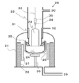
- the CZ silicon single crystal (single crystal rod) 23 doped with gallium is pulled using the CZ single crystal manufacturing apparatus 20 of FIG.
- a CZ single crystal manufacturing apparatus 20 includes a main chamber 21 in which a heater 27 and a quartz crucible 25 for containing a raw material melt 24 are disposed, a pulling chamber 22 provided on the main chamber 21, A cooling cylinder 31 is provided which extends downward from the ceiling of the chamber 21 and is provided immediately above the raw material melt 24 to cool the pulled single crystal rod 23.
- a gas outlet 29 can be provided in the lower part of the main chamber 21, and a gas inlet 30 can be provided in the upper part of the pulling chamber 22.
- the quartz crucible 25 is supported by, for example, a graphite crucible 26, and the graphite crucible 26 is supported by, for example, a crucible rotating shaft 36.
- a heat insulating member 28 is provided outside the heater 27 that heats the quartz crucible 25 so as to surround the periphery.
- a pulling mechanism (not shown) is provided on the upper portion of the pulling chamber 22.
- a pulling wire 33 is unwound from the pulling mechanism.
- a seed holder 35 for attachment is connected.
- the cooling cylinder 31 is provided with, for example, a refrigerant inlet 32.
- step S11 for example, by introducing a predetermined amount of gallium into the quartz crucible 25, gallium can be doped into the single crystal to be grown.
- the FZ silicon single crystal is manufactured by using the CZ silicon single crystal manufactured in step S11 as a raw material rod and subjecting the raw material rod to a float zone treatment at 1.6 atm or higher (see step S12 in FIG. 1).
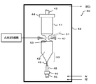
- the gallium-doped CZ silicon single crystal manufactured by the CZ method using the FZ single crystal manufacturing apparatus 40 of FIG. 4 is placed in the chamber 52 of the FZ single crystal manufacturing apparatus 40.
- the upper holding jig 44 is fixed to the upper holding jig 44 with screws or the like to form a raw material rod 41, and the lower holding jig 46 of the lower shaft 45 is attached with a seed crystal 48 having a small diameter.
- the lower end of the cone portion 53 of the raw material rod 41 (in FIG. 4, since the float zone process has been progressed to some extent, the cone portion 53 is illustrated as the cone portion of the FZ single crystal rod 42).
- Ar gas containing nitrogen gas is supplied from the lower part of the chamber 52, exhausted from the upper part of the chamber 52, and the pressure in the chamber 52 is increased to 1.6 atmospheres or more.
- the flow rate of Ar gas can be 20 l / min, and the nitrogen concentration in the chamber can be 0.5%.
- the raw material rod 41 is heated and melted by an induction heating coil (high frequency coil) 47
- the tip of the cone portion 53 is fused to the seed crystal 48
- dislocation is eliminated by the throttle portion 49
- the upper shaft 43 and the lower shaft 45 are rotated.
- the floating zone (float zone) 50 is moved to the upper end of the raw material rod 41 for zoning, and the raw material rod 41 is recrystallized to produce a single crystal rod. Grow 42.
- step S12 it is preferable that dopant gas is sprayed from the dopant gas spray nozzle 51 to the floating zone 50 to further dope gallium to the FZ silicon single crystal.
- the gallium evaporated during the float zone process can be supplemented by additionally doping gallium into the FZ silicon single crystal using the dopant gas. It is possible to more effectively suppress the resistance.
- the axis of the gallium concentration of the FZ silicon single crystal is changed by changing the flow rate and / or concentration of the dopant gas in the axial direction according to the axial distribution of the gallium concentration of the CZ silicon single crystal. It is preferable to make the direction distribution uniform. By uniforming the axial distribution of the gallium concentration of the FZ silicon single crystal in this way, variation in the resistivity in the axial direction of the FZ silicon single crystal can be suppressed, and the FZ silicon single crystal manufactured in this way Yield (ratio of the region where the resistivity falls within the standard) can be improved.
- any of an organic gallium compound, a gallium halide compound, and gallium hydride can be used as the dopant gas.
- the above gas can be suitably used as a dopant gas for additionally doping gallium.
- the float zone treatment is preferably performed in an atmosphere containing argon or helium.
- the FZ silicon single crystal to be manufactured has a diameter of 150 mm or more.
- the float zone also becomes large and gallium is likely to evaporate, so that the present invention can be suitably applied.
- the FZ silicon single crystal is manufactured by carrying out the float zone process of the raw material stick
- the evaporation amount of the dopant can be suppressed, and the increase in resistance of the FZ silicon single crystal can be suppressed.
- oxygen inevitably entering the CZ crystal can be reduced by outward diffusion.
- boron is not used as a dopant. Therefore, it is possible to prevent the formation of a B—O pair which is a problem with respect to the characteristics of the solar cell. In the method of the present invention, these can be achieved simultaneously. For this reason, if a solar cell is manufactured using the silicon substrate manufactured from the FZ silicon single crystal for solar cells manufactured in this way, the conversion efficiency of the manufactured solar cell can be improved.
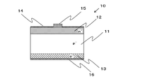
- the solar cell 10 of FIG. 2 is manufactured using the FZ silicon single crystal manufactured using the method for manufacturing a solar cell FZ silicon single crystal described above.
- the solar cell 10 includes a gallium-doped silicon substrate 11 cut out from an FZ silicon single crystal, an emitter layer (phosphorus diffusion layer) 12 provided on the light-receiving surface side of the gallium-doped silicon substrate 11, and a back surface of the gallium-doped silicon substrate 11. And a BSF layer (aluminum diffusion layer) 13 provided on the side, and a light receiving surface antireflection film 14 is provided on the light receiving surface side surface of the emitter layer 12.
- the solar cell 10 further includes a light receiving surface electrode 15 provided on the light receiving surface side surface of the emitter layer 12 and a back surface aluminum electrode 16 provided on the back surface side of the BSF layer 13.
- the light receiving surface electrode 15 penetrates the light receiving surface antireflection film 14 and is electrically connected to the emitter layer 12, and the back surface aluminum electrode 16 is electrically connected to the BSF layer 13. .
- the oxygen that inevitably enters the CZ crystal is reduced, the formation of B—O pairs that are problematic for the characteristics of the solar cell is prevented, and the increase in resistance is suppressed. Since the manufactured FZ silicon single crystal is used, the conversion efficiency of the solar cell can be improved.
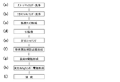
- cleaning is performed after removing the damaged layer of the gallium-doped silicon substrate 11 cut out from the silicon single crystal ingot (see FIG. 5A).
- the removal of the damaged layer can be performed, for example, by immersing the gallium-doped silicon substrate 11 in a hot concentrated potassium hydroxide aqueous solution.
- the gallium doped silicon substrate 11 from which the damaged layer has been removed is subjected to texture etching and then cleaned (see FIG. 5B).
- Texture etching can be performed, for example, by dipping in an aqueous solution of potassium hydroxide / 2-propanol. By performing texture etching, fine unevenness called texture can be formed, and the reflectance of the light receiving surface can be reduced.
- a diffusion mask for forming the emitter layer (phosphorus diffusion layer) 12 is formed on the gallium-doped silicon substrate 11 subjected to texture etching (see FIG. 5C).
- the diffusion mask can be formed by placing the gallium-doped silicon substrate 11 in a horizontal furnace, growing an oxide film by thermal oxidation, and etching one side.
- Phosphorus diffusion is performed on the gallium-doped silicon substrate 11 on which the diffusion mask is formed (see FIG. 5D).
- Phosphorus diffusion can be performed, for example, by placing the gallium-doped silicon substrate 11 in a horizontal furnace and performing a heat treatment in an oxygen and POCl 3 gas atmosphere.
- two gallium doped substrates 11 are put in one groove of a quartz boat at the time of diffusion so that POCl 3 gas does not wrap around on one side, and the other side It is also possible to form a phosphorus diffusion layer.
- a light-receiving surface antireflection film 14 is formed on the light-receiving surface-side surface of the emitter layer 12 of the gallium-doped silicon substrate 11 (see FIG. 5F).
- the formation of the light-receiving surface antireflection film 14 can be performed, for example, by forming a silicon nitride film by plasma CVD.
- a back surface aluminum electrode 16 is formed on the back surface of the gallium-doped silicon substrate 11 (see FIG. 5G).
- the back surface aluminum electrode 16 can be formed, for example, by screen-printing Al paste on a portion other than the bus bar electrode portion on the back surface of the gallium-doped silicon substrate 11.
- a silver electrode (not shown) is formed by screen printing using a silver paste on the bus bar electrode portion on the back surface of the gallium-doped silicon substrate 11.
- a light receiving surface electrode 15 is formed on the light receiving surface side surface of the light receiving surface antireflection film 14 (see FIG. 5H).
- the formation of the light receiving surface electrode 15 can be performed, for example, by screen printing in a desired pattern using a silver paste.
- the gallium-doped silicon substrate 11 on which the back surface aluminum electrode 16 and the light receiving surface electrode 15 have been formed is baked (see FIG. 5I).
- aluminum diffuses from the back surface aluminum electrode 16 into the gallium-doped silicon substrate 11 to form a BSF layer (aluminum diffusion layer) 13.
- the light-receiving surface electrode 15 and the emitter layer 12 can be electrically connected by passing the film through the light-receiving surface electrode 15 during firing without opening the light-receiving surface antireflection film 14.
- Example 1 An FZ silicon single crystal was manufactured by the manufacturing method described with reference to FIG. However, the pressure during the float zone treatment was 1.6 atmospheres, and additional gallium doping with the dopant gas during the float zone treatment was not performed.
- the solar cell 10 of FIG. 2 was manufactured by the manufacturing method demonstrated using FIG. 5 using the gallium dope silicon substrate cut out from the manufactured FZ silicon single crystal.
- the characteristics (short circuit current density, open voltage, fill factor, conversion efficiency) of the solar cell were measured.
- the results are shown in Table 1.
- the short-circuit current density is the current density value when the resistance of the resistor connected to the solar cell is 0 ⁇
- the open circuit voltage is the voltage when the resistance of the resistor connected to the solar cell is very large.
- the fill factor (shape factor) is the maximum generated power / (short circuit current ⁇ open circuit voltage), and the conversion efficiency is (output from the solar cell / solar energy entering the solar cell) ⁇ 100.
- Example 2 In the same manner as in Example 1, an FZ silicon single crystal was produced. However, the pressure during the float zone treatment was 1.8 atm.
- the solar cell 10 of FIG. 2 was manufactured by the manufacturing method demonstrated using FIG. 5 using the gallium dope silicon substrate cut out from the manufactured FZ silicon single crystal.
- Example 3 In the same manner as in Example 1, an FZ silicon single crystal was produced. However, the pressure during the float zone treatment was 2.0 atm.
- the solar cell 10 of FIG. 2 was manufactured by the manufacturing method demonstrated using FIG. 5 using the gallium dope silicon substrate cut out from the manufactured FZ silicon single crystal.
- Example 4 In the same manner as in Example 1, an FZ silicon single crystal was produced. However, additional gallium doping with a dopant gas was performed during the float zone treatment.
- the solar cell 10 of FIG. 2 was manufactured by the manufacturing method demonstrated using FIG. 5 using the gallium dope silicon substrate cut out from the manufactured FZ silicon single crystal.
- Example 1 In the same manner as in Example 1, an FZ silicon single crystal was produced. However, the pressure during the float zone treatment was 1.2 atm.
- the solar cell 10 of FIG. 2 was manufactured by the manufacturing method demonstrated using FIG. 5 using the gallium dope silicon substrate cut out from the manufactured FZ silicon single crystal.
- Example 2 In the same manner as in Example 1, an FZ silicon single crystal was produced. However, the pressure during the float zone treatment was 1.4 atm.
- the solar cell 10 of FIG. 2 was manufactured by the manufacturing method demonstrated using FIG. 5 using the gallium dope silicon substrate cut out from the manufactured FZ silicon single crystal.
- Example 3 In the same manner as in Example 1, an FZ silicon single crystal was produced. However, boron was used as a dopant. Using the boron-doped silicon substrate cut out from the manufactured FZ silicon single crystal, a solar cell was manufactured by the manufacturing method described with reference to FIG.
- Example 1-4 in which the pressure during the float zone treatment is 1.6 atmospheres or more is compared with Comparative Example 1-2 where the pressure during the float zone treatment is less than 1.6 atmospheres. Conversion efficiency is improved. Further, in Example 1 in which the dopant is gallium, the conversion efficiency is improved as compared with Comparative Example 3 in which the dopant is boron. Furthermore, in Example 1 in which the silicon single crystal was manufactured by the FZ method using the CZ crystal as a raw material rod, the conversion efficiency was improved as compared with Comparative Example 4 in which the silicon single crystal was manufactured by the CZ method.
- Example 4 in which the additional gallium doping with the dopant gas was performed, the conversion efficiency was further improved as compared with Example 1-3 in which the additional gallium doping with the dopant gas was not performed, and the ratio of the crystals having the desired resistivity (Yield) improved.
- the present invention is not limited to the above embodiment.
- the above-described embodiment is an exemplification, and the present invention has substantially the same configuration as the technical idea described in the claims of the present invention, and any device that exhibits the same function and effect is the present invention. It is included in the technical scope of the invention.
Landscapes
- Chemical & Material Sciences (AREA)
- Crystallography & Structural Chemistry (AREA)
- Engineering & Computer Science (AREA)
- Materials Engineering (AREA)
- Metallurgy (AREA)
- Organic Chemistry (AREA)
- Crystals, And After-Treatments Of Crystals (AREA)
- Photovoltaic Devices (AREA)
- Life Sciences & Earth Sciences (AREA)
- Sustainable Development (AREA)
Abstract
本発明は、太陽電池用のFZシリコン単結晶の製造方法であって、チョクラルスキー法により、ガリウムがドープされたCZシリコン単結晶を引き上げる工程と、前記CZシリコン単結晶を原料棒として、該原料棒を1.6気圧以上でフロートゾーン処理することにより、FZシリコン単結晶を製造する工程とを含むことを特徴とする太陽電池用FZシリコン単結晶の製造方法である。これにより、CZ結晶に不可避的に入る酸素を低減させ、太陽電池の特性に対して問題となるB-Oペアの生成を防止しながらも、フロートゾーン処理中のガリウムドーパントの蒸発量を抑制し、シリコン単結晶が高抵抗化することを防止することができる太陽電池用FZシリコン単結晶の製造方法が提供される。
Description
本発明は、太陽電池用FZシリコン単結晶の製造方法、及びFZシリコン単結晶を用いて製造された太陽電池に関する。
単結晶シリコンの製造方法には、石英るつぼ内に高純度ポリシリコンを溶かし、それに種結晶を接触させてゆっくりと成長、引き上げを行うCZ(Czochralsky)法と、棒状の高純度ポリシリコンの一部を加熱し、種結晶となる下部の単結晶と棒状の原料結晶(ポリシリコン等)との間に溶融部を作り、その融液部を表面張力によって支えながら全体を下方に移動させ、融液部を冷却して単結晶を得るFZ(Float Zone)法とがある。
CZ法で製造したシリコン単結晶には石英るつぼからの酸素の混入があり、その濃度が高ければ、酸素欠陥核を多数保有していることになる。一方、上記のFZ法で製造したシリコン結晶は、酸素含有量が少ないことから、酸素欠陥核が少ない。
また、CZ法により作製したCZシリコン単結晶を原料棒として用いて、FZ法によりFZシリコン単結晶を作製することが特許文献1に開示されており、このようにして作製したFZシリコン単結晶も酸素含有量が少ないことも特許文献1に開示されている。
また、CZ法により作製したCZシリコン単結晶を原料棒として用いて、FZ法によりFZシリコン単結晶を作製することが特許文献1に開示されており、このようにして作製したFZシリコン単結晶も酸素含有量が少ないことも特許文献1に開示されている。
また、太陽電池に用いられるシリコン基板として、少数キャリアのライフタイムの低下を抑制するために、ガリウムがドーピングされたp型シリコン基板を用いることが知られている(例えば、特許文献2を参照)。
本発明者は、CZシリコン単結晶を原料棒として用いてFZ法で製造したFZシリコン単結晶から太陽電池を製造すると、シリコン単結晶中の酸素含有量が少ないことから、酸素欠陥ができにくいため、CZ法で作製したCZシリコン結晶から製造する場合とは異なり、全く同一のプロセスを経ても、酸素欠陥に起因する少数キャリアのライフタイムの低下が抑制され、高い変換効率の太陽電池を製造することが可能であることを見出した。本発明者は、さらに、ガリウムがドーピングされたp型シリコン基板を用いることにより少数キャリアのライフタイムを向上させることに着目して、太陽電池用シリコン単結晶をガリウムドープさせたCZシリコン単結晶を原料棒として用いてFZ法で製造することを試みた。
しかしながら、ガリウムドープさせたCZシリコン単結晶を原料棒として用いてFZ法でガリウムドープのFZシリコン単結晶を製造しようとすると、原料棒のフロートゾーンの溶融時にドーパントであるガリウムが蒸発して、非常に高抵抗のガリウムドープFZシリコン単結晶しか得られず、このようなシリコン単結晶を用いて太陽電池を製造すると、内部抵抗が高くなりすぎて、変換効率が低下するという問題があった。
本発明は、上記問題点に鑑みてなされたものであって、CZ結晶に不可避的に入る酸素を低減させ、太陽電池の特性に対して問題となるB-Oペアの生成を防止しながらも、フロートゾーン処理中のガリウムドーパントの蒸発量を抑制し、FZシリコン単結晶が高抵抗化することを防止することができる太陽電池用FZシリコン単結晶の製造方法を提供することを目的とする。
上記目的を達成するために、本発明は、太陽電池用のFZシリコン単結晶の製造方法であって、チョクラルスキー法により、ガリウムがドープされたCZシリコン単結晶を引き上げる工程と、前記CZシリコン単結晶を原料棒として、該原料棒を1.6気圧以上でフロートゾーン処理することにより、FZシリコン単結晶を製造する工程とを含むことを特徴とする太陽電池用FZシリコン単結晶の製造方法を提供する。
このように原料棒を1.6気圧以上でフロートゾーン処理することによりFZシリコン単結晶を製造することで、フロートゾーン処理中のガリウムドーパントの蒸発量を抑制することができ、それによってFZシリコン単結晶が高抵抗化することを抑制することができる。また、CZシリコン単結晶をフロートゾーン処理するので、CZ結晶に不可避的に入る酸素を外方拡散により低減することができる。また、ガリウムドープ基板であるので、ドーパントとしてホウ素を用いない。従って、太陽電池の特性に対して問題となるB-Oペアの生成を防止できる。このため、このようにして製造された太陽電池用FZシリコン単結晶から作製されたシリコン基板を用いて太陽電池を製造すれば、製造された太陽電池の変換効率を向上させることができる。
このとき、前記フロートゾーン処理において、ドーパントガスを用いて、前記FZシリコン単結晶にガリウムを追加ドープすることが好ましい。
このように、フロートゾーン処理において、ドーパントガスを用いて、FZシリコン単結晶にガリウムを追加ドープすることで、フロートゾーン処理中に蒸発したガリウムを補うことができ、それによりFZシリコン単結晶が高抵抗化することをより効果的に抑制することができる。
このとき、前記ガリウムの追加ドープにおいて、前記CZシリコン単結晶のガリウム濃度の軸方向分布に応じて、軸方向で前記ドーパントガスの流量及び/又は濃度を変化させることにより、前記FZシリコン単結晶のガリウム濃度の軸方向分布を均一化することが好ましい。
このようにFZシリコン単結晶のガリウム濃度の軸方向分布を均一化することで、FZシリコン単結晶の軸方向の抵抗率のばらつきを抑えることができ、このようにして製造されたFZシリコン単結晶の歩留まり(抵抗率が規格内に入る領域の割合)を向上させることができる。
このとき、前記ドーパントガスとして、有機ガリウム化合物、ハロゲン化ガリウム化合物及び水素化ガリウムのいずれかを用いることができる。
ガリウムを追加ドープするためのドーパントガスとして、上記のガスを好適に用いることができる。
このとき、前記フロートゾーン処理を、アルゴン又はヘリウムを含有する雰囲気下で行うことが好ましい。
フロートゾーン処理を上記のような雰囲気下で行うことで、FZシリコン単結晶中に不純物が取り込まれることを防止することができる。
このとき、前記製造するFZシリコン単結晶を直径150mm以上とすることが好ましい。
製造するFZシリコン単結晶が直径150mm以上である場合に、ドーパントがより蒸発しやすいので、本発明を好適に適用することができる。
上記目的を達成するために、本発明は、上記の太陽電池用FZシリコン単結晶の製造方法により製造したFZシリコン単結晶を用いて製造されたものであることを特徴とする太陽電池を提供する。
このような太陽電池であれば、基板として用いるシリコン単結晶基板が高抵抗化することを抑制することができるので、太陽電池の変換効率を向上させることができる。
以上のように、本発明の太陽電池用FZシリコン単結晶の製造方法によれば、原料棒を1.6気圧以上でフロートゾーン処理することによりFZシリコン単結晶を製造することで、フロートゾーン処理中のガリウムドーパントの蒸発量を抑制することができる。また、それによってFZシリコン単結晶が高抵抗化することを抑制することができ、このようにして製造された太陽電池用FZシリコン単結晶から作製されたシリコン基板を用いて太陽電池を製造すれば、製造された太陽電池の変換効率を向上させることができる。また、本発明の太陽電池であれば、基板として用いるシリコン単結晶基板が高抵抗化することを抑制することができるので、太陽電池の変換効率を向上させることができる。
以下、本発明について、実施態様の一例として、図を参照しながら詳細に説明するが、本発明はこれに限定されるものではない。
前述のように、本発明者は、基板中の少数キャリアのライフタイムの低下を抑制するために、太陽電池用シリコン単結晶をガリウムドープさせたCZシリコン単結晶を原料棒として用いてFZ法で製造することを試みたが、原料棒のフロートゾーンの溶融時にドーパントであるガリウムが蒸発して、非常に高抵抗のガリウムドープFZシリコン単結晶しか得られず、このようなシリコン単結晶を用いて太陽電池を製造すると、内部抵抗が高くなりすぎて、変換効率が低下するという問題があった。
そこで、発明者は、フロートゾーン処理中のガリウムドーパントの蒸発量を抑制し、FZシリコン単結晶が高抵抗化することを防止することができる太陽電池用FZシリコン単結晶の製造方法について鋭意検討を重ねた。その結果、原料棒を1.6気圧以上でフロートゾーン処理することによりFZシリコン単結晶を製造することで、フロートゾーン処理中のガリウムドーパントの蒸発量を抑制することができ、それによってFZシリコン単結晶が高抵抗化することを抑制することができることを見出し、本発明をなすに至った。
以下、図1、3-4を参照しながら、本発明の太陽電池用FZシリコン単結晶の製造方法を説明する。
まず、CZ法により、ガリウムがドープされたCZシリコン単結晶を引上げる(図1のステップS11を参照)。CZ法としては種々の方法を用いることできる。具体的には、例えば、図3のCZ単結晶製造装置20を用いて、ガリウムがドープされたCZシリコン単結晶(単結晶棒)23を引上げる。図3において、CZ単結晶製造装置20は、加熱ヒータ27と原料融液24を収容する石英ルツボ25とが配置されたメインチャンバー21と、メインチャンバー21上に設けられた引上げチャンバー22と、メインチャンバー21の天井部より下方に延設され、原料融液24の直上に設けられ、引上げられた単結晶棒23を冷却する冷却筒31とを有している。メインチャンバー21の下部にはガス流出口29を設けることができ、引上げチャンバー22の上部にはガス導入口30を設けることができる。石英ルツボ25は、例えば、黒鉛ルツボ26によって支持され、黒鉛ルツボ26は、例えば、ルツボ回転軸36によって支持される。石英ルツボ25を加熱する加熱ヒータ27の外側には、例えば、断熱部材28が周囲を取り囲むように設けられている。引上げチャンバー22の上部には、例えば、引上げ機構(不図示)が設けられており、引上げ機構からは、例えば、引上げワイヤ33が巻出されており、その先端には、例えば、種結晶34を取り付けるための種ホルダ35が接続されている。冷却筒31には、例えば、冷媒導入口32が設けられている。ステップS11において、例えば、石英ルツボ25内にガリウムを所定の量だけ投入することにより、育成される単結晶中にガリウムをドープすることができる。
次に、ステップS11で製造したCZシリコン単結晶を原料棒として、原料棒を1.6気圧以上でフロートゾーン処理することにより、FZシリコン単結晶を製造する(図1のステップS12を参照)。具体的には、例えば、図4のFZ単結晶製造装置40を用いて、CZ法により製造されたガリウムドープCZシリコン単結晶を、FZ単結晶製造装置40のチャンバー52内に設置された上軸43の上部保持冶具44にネジ等で固定して原料棒41とし、下軸45の下部保持冶具46には直径の小さい種結晶48を取り付ける。次いで、原料棒41のコーン部53(図4中では、ある程度フロートゾーン処理が進んだ状態を示しているため、コーン部53はFZ単結晶棒42のコーン部として図示している)の下端をカーボンリング(不図示)で予備加熱し、その後、チャンバー52の下部より窒素ガスを含んだArガスを供給して、チャンバー52上部より排気して、チャンバー52内の圧力を1.6気圧以上にする。例えば、Arガスの流量を20l/min、チャンバー内窒素濃度を0.5%とすることができる。そして、原料棒41を誘導加熱コイル(高周波コイル)47で加熱溶融した後、コーン部53先端を種結晶48に融着させ、絞り部49により無転位化し、上軸43と下軸45を回転させながら原料棒41を例えば2.0mm/minの成長速度で下降させることで浮遊帯域(フロートゾーン)50を原料棒41上端まで移動させてゾーニングし、原料棒41を再結晶化して単結晶棒42を成長させる。
ここで、ステップS12のフロートゾーン処理において、ドーパントガス吹き付け用ノズル51からドーパントガスを浮遊帯域50に吹き付けて、FZシリコン単結晶にガリウムを追加ドープすることが好ましい。このように、フロートゾーン処理において、ドーパントガスを用いて、FZシリコン単結晶にガリウムを追加ドープすることで、フロートゾーン処理中に蒸発したガリウムを補うことができ、それによりFZシリコン単結晶が高抵抗化することをより効果的に抑制することができる。
ここで、ガリウムの追加ドープにおいて、CZシリコン単結晶のガリウム濃度の軸方向分布に応じて、軸方向でドーパントガスの流量及び/又は濃度を変化させることにより、FZシリコン単結晶のガリウム濃度の軸方向分布を均一化することが好ましい。このようにFZシリコン単結晶のガリウム濃度の軸方向分布を均一化することで、FZシリコン単結晶の軸方向の抵抗率のばらつきを抑えることができ、このようにして製造されたFZシリコン単結晶の歩留まり(抵抗率が規格内に入る領域の割合)を向上させることができる。
ここで、ドーパントガスとして、有機ガリウム化合物、ハロゲン化ガリウム化合物及び水素化ガリウムのいずれかを用いることができる。ガリウムを追加ドープするためのドーパントガスとして、上記のガスを好適に用いることができる。
ここで、フロートゾーン処理を、アルゴン又はヘリウムを含有する雰囲気下で行うことが好ましい。フロートゾーン処理を上記のような雰囲気下で行うことで、FZシリコン単結晶中に不純物が取り込まれることを防止することができる。
ここで、製造するFZシリコン単結晶を直径150mm以上とすることが好ましい。直径150mm以上の太陽電池用FZシリコン単結晶を製造する場合に、フロートゾーンも大きくなり、ガリウムの蒸発も生じやすくなるので、本発明を好適に適用することができる。
上記で説明した太陽電池用FZシリコン単結晶の製造方法であれば、原料棒41を1.6気圧以上でフロートゾーン処理することによりFZシリコン単結晶を製造することで、フロートゾーン処理中のガリウムドーパントの蒸発量を抑制することができ、FZシリコン単結晶の高抵抗化を抑制できる。また、CZシリコン単結晶をフロートゾーン処理するので、CZ結晶に不可避的に入る酸素を外方拡散により低減することができる。また、ガリウムドープ基板であるので、ドーパントとしてホウ素を用いない。従って、太陽電池の特性に対して問題となるB-Oペアの生成を防止できる。本発明の方法では、これらを同時に達成できる。このため、このようにして製造された太陽電池用FZシリコン単結晶から作製されたシリコン基板を用いて太陽電池を製造すれば、製造された太陽電池の変換効率を向上させることができる。
次に、図2を参照しながら、本発明の太陽電池を説明する。
図2の太陽電池10は、上記で説明した太陽電池用FZシリコン単結晶の製造方法を用いて製造したFZシリコン単結晶を用いて製造されているものである。太陽電池10は、FZシリコン単結晶から切り出されたガリウムドープシリコン基板11と、ガリウムドープシリコン基板11の受光面側に設けられたエミッタ層(リン拡散層)12と、ガリウムドープシリコン基板11の裏面側に設けられたBSF層(アルミニウム拡散層)13とを有しており、エミッタ層12の受光面側表面には受光面反射防止膜14が設けられている。太陽電池10は、さらに、エミッタ層12の受光面側表面上に設けられた受光面電極15と、BSF層13の裏面側表面に設けられた裏面アルミニウム電極16とを有している。なお、太陽電池10において、受光面電極15は受光面反射防止膜14を貫通してエミッタ層12と電気的に接続されており、裏面アルミニウム電極16はBSF層13と電気的に接続されている。
このような太陽電池であれば、CZ結晶に不可避的に入る酸素を低減させ、太陽電池の特性に対して問題となるB-Oペアの生成が防止され、かつ、高抵抗化することが抑制されたFZシリコン単結晶を用いて製造されているものであるので、太陽電池の変換効率を向上させることができる。
次に、図5を参照しながら、図2の太陽電池10の製造方法の一例を具体的に説明する。
まず、シリコン単結晶インゴットから切り出したガリウムドープシリコン基板11のダメージ層を除去してから洗浄を行う(図5(a)を参照)。ダメージ層の除去は、例えば、ガリウムドープシリコン基板11を熱濃水酸化カリウム水溶液中に浸漬することで行うことができる。
次に、ダメージ層を除去したガリウムドープシリコン基板11に対してテクスチャエッチングを行ってから洗浄を行う(図5(b)を参照)。テクスチャエッチングは、例えば、水酸化カリウム/2-プロパノールの水溶液中に浸漬することで行うことができる。なお、テクスチャエッチングを行うことでテクスチャと呼ばれる微細な凹凸を形成することができ、受光面の反射率を低減することができる。
次に、テクスチャエッチングを行ったガリウムドープシリコン基板11に対してエミッタ層(リン拡散層)12形成用の拡散マスクを形成する(図5(c)を参照)。拡散マスクの形成は、ガリウムドープシリコン基板11を横型炉に入れ、熱酸化により酸化膜を成長させ、片面をエッチングすることで行うことができる。
次に、拡散マスクを形成したガリウムドープシリコン基板11に対してリン拡散を行う(図5(d)を参照)。リン拡散は、例えば、ガリウムドープシリコン基板11を横型炉に入れ、酸素およびPOCl3ガス雰囲気の中で熱処理することで行うことができる。製造コストを低減するために、上記の拡散マスクを形成せずに、拡散時にガリウムドープ基板11を石英ボートの一溝に2枚入れ、片面にPOCl3ガスが回り込まないようにして、他方の片面にリン拡散層を形成することも可能である。
次に、ガリウムドープシリコン基板11の表面に形成されたリンガラスおよび酸化珪素膜をふっ酸で除去する(図5(e)を参照)。
次に、ガリウムドープシリコン基板11のエミッタ層12の受光面側表面に受光面反射防止膜14を形成する(図5(f)を参照)。受光面反射防止膜14の形成は、例えば、プラズマCVDにより窒化珪素膜を形成することで行うことができる。
次に、ガリウムドープシリコン基板11の裏面側表面に裏面アルミニウム電極16を形成する(図5(g)を参照)。裏面アルミニウム電極16の形成は、例えば、Alペーストをガリウムドープシリコン基板11の裏面のバスバー電極部以外にスクリーン印刷することで行うことができる。引き続き、ガリウムドープシリコン基板11の裏面のバスバー電極部に銀ペーストを用いて、スクリーン印刷により銀電極(不図示)を形成する。
次に、受光面反射防止膜14の受光面側表面に受光面電極15を形成する(図5(h)を参照)。受光面電極15の形成は、例えば、銀ペーストを用いて所望のパターンにスクリーン印刷することで行うことができる。
次に、裏面アルミニウム電極16及び受光面電極15の形成を行ったガリウムドープシリコン基板11に対して焼成を行う(図5(i)を参照)。この焼成時に、裏面アルミニウム電極16からアルミニウムがガリウムドープシリコン基板11内に拡散し、BSF層(アルミニウム拡散層)13が形成される。なお、受光面反射防止膜14を開口せずに、焼成時に受光面電極15にこの膜を貫通させることにより、受光面電極15とエミッタ層12を電気的に接続させることができる。
上記のようにして、図2の太陽電池10を製造することができる。
以下、実施例及び比較例を示して本発明をより具体的に説明するが、本発明はこれらに限定されるものではない。
(実施例1)
図1を用いて説明した製造方法でFZシリコン単結晶を製造した。ただし、フロートゾーン処理時の圧力は1.6気圧とし、フロートゾーン処理時のドーパントガスによる追加ガリウムドープは行わなかった。製造したFZシリコン単結晶から切り出したガリウムドープシリコン基板を用いて、図5を用いて説明した製造方法により、図2の太陽電池10を製造した。
図1を用いて説明した製造方法でFZシリコン単結晶を製造した。ただし、フロートゾーン処理時の圧力は1.6気圧とし、フロートゾーン処理時のドーパントガスによる追加ガリウムドープは行わなかった。製造したFZシリコン単結晶から切り出したガリウムドープシリコン基板を用いて、図5を用いて説明した製造方法により、図2の太陽電池10を製造した。
製造した太陽電池について、太陽電池の特性(短絡電流密度、開放電圧、フィルファクタ、変換効率)を測定した。その結果を表1に示す。ここで、短絡電流密度は、太陽電池に接続される抵抗器の抵抗が0Ωの時の電流密度値であり、開放電圧は、太陽電池に接続される抵抗器の抵抗が非常に大きい時の電圧値であり、フィルファクタ(形状因子)は、最大発電電力/(短絡電流×開放電圧)であり、変換効率は、(太陽電池からの出力/太陽電池に入った太陽エネルギー)×100である。
(実施例2)
実施例1と同様にして、FZシリコン単結晶を製造した。ただし、フロートゾーン処理時の圧力は1.8気圧とした。製造したFZシリコン単結晶から切り出したガリウムドープシリコン基板を用いて、図5を用いて説明した製造方法により、図2の太陽電池10を製造した。
実施例1と同様にして、FZシリコン単結晶を製造した。ただし、フロートゾーン処理時の圧力は1.8気圧とした。製造したFZシリコン単結晶から切り出したガリウムドープシリコン基板を用いて、図5を用いて説明した製造方法により、図2の太陽電池10を製造した。
製造した太陽電池について、太陽電池の特性(短絡電流密度、開放電圧、フィルファクタ、変換効率)を測定した。その結果を表1に示す。
(実施例3)
実施例1と同様にして、FZシリコン単結晶を製造した。ただし、フロートゾーン処理時の圧力は2.0気圧とした。製造したFZシリコン単結晶から切り出したガリウムドープシリコン基板を用いて、図5を用いて説明した製造方法により、図2の太陽電池10を製造した。
実施例1と同様にして、FZシリコン単結晶を製造した。ただし、フロートゾーン処理時の圧力は2.0気圧とした。製造したFZシリコン単結晶から切り出したガリウムドープシリコン基板を用いて、図5を用いて説明した製造方法により、図2の太陽電池10を製造した。
製造した太陽電池について、太陽電池の特性(短絡電流密度、開放電圧、フィルファクタ、変換効率)を測定した。その結果を表1に示す。
(実施例4)
実施例1と同様にして、FZシリコン単結晶を製造した。ただし、フロートゾーン処理時にドーパントガスによる追加ガリウムドープを行った。製造したFZシリコン単結晶から切り出したガリウムドープシリコン基板を用いて、図5を用いて説明した製造方法により、図2の太陽電池10を製造した。
実施例1と同様にして、FZシリコン単結晶を製造した。ただし、フロートゾーン処理時にドーパントガスによる追加ガリウムドープを行った。製造したFZシリコン単結晶から切り出したガリウムドープシリコン基板を用いて、図5を用いて説明した製造方法により、図2の太陽電池10を製造した。
製造した太陽電池について、太陽電池の特性(短絡電流密度、開放電圧、フィルファクタ、変換効率)を測定した。その結果を表1に示す。
(比較例1)
実施例1と同様にして、FZシリコン単結晶を製造した。ただし、フロートゾーン処理時の圧力は1.2気圧とした。製造したFZシリコン単結晶から切り出したガリウムドープシリコン基板を用いて、図5を用いて説明した製造方法により、図2の太陽電池10を製造した。
実施例1と同様にして、FZシリコン単結晶を製造した。ただし、フロートゾーン処理時の圧力は1.2気圧とした。製造したFZシリコン単結晶から切り出したガリウムドープシリコン基板を用いて、図5を用いて説明した製造方法により、図2の太陽電池10を製造した。
製造した太陽電池について、太陽電池の特性(短絡電流密度、開放電圧、フィルファクタ、変換効率)を測定した。その結果を表1に示す。
(比較例2)
実施例1と同様にして、FZシリコン単結晶を製造した。ただし、フロートゾーン処理時の圧力は1.4気圧とした。製造したFZシリコン単結晶から切り出したガリウムドープシリコン基板を用いて、図5を用いて説明した製造方法により、図2の太陽電池10を製造した。
実施例1と同様にして、FZシリコン単結晶を製造した。ただし、フロートゾーン処理時の圧力は1.4気圧とした。製造したFZシリコン単結晶から切り出したガリウムドープシリコン基板を用いて、図5を用いて説明した製造方法により、図2の太陽電池10を製造した。
製造した太陽電池について、太陽電池の特性(短絡電流密度、開放電圧、フィルファクタ、変換効率)を測定した。その結果を表1に示す。
(比較例3)
実施例1と同様にして、FZシリコン単結晶を製造した。ただし、ドーパントとしてボロンを用いた。製造したFZシリコン単結晶から切り出したボロンドープシリコン基板を用いて、図5を用いて説明した製造方法により、太陽電池を製造した。
実施例1と同様にして、FZシリコン単結晶を製造した。ただし、ドーパントとしてボロンを用いた。製造したFZシリコン単結晶から切り出したボロンドープシリコン基板を用いて、図5を用いて説明した製造方法により、太陽電池を製造した。
製造した太陽電池について、太陽電池の特性(短絡電流密度、開放電圧、フィルファクタ、変換効率)を測定した。その結果を表1に示す。
(比較例4)
CZ法により、ガリウムドープされたCZシリコン単結晶を製造した。製造したCZシリコン単結晶から切り出したガリウムドープシリコン基板を用いて、図5を用いて説明した製造方法により、図2の太陽電池10を製造した。
CZ法により、ガリウムドープされたCZシリコン単結晶を製造した。製造したCZシリコン単結晶から切り出したガリウムドープシリコン基板を用いて、図5を用いて説明した製造方法により、図2の太陽電池10を製造した。
製造した太陽電池について、太陽電池の特性(短絡電流密度、開放電圧、フィルファクタ、変換効率)を測定した。その結果を表1に示す。

表1からわかるように、フロートゾーン処理時の圧力が1.6気圧以上である実施例1-4では、フロートゾーン処理時の圧力が1.6気圧未満である比較例1-2と比較して変換効率が向上している。また、ドーパントをガリウムとした実施例1では、ドーパントをボロンとした比較例3と比較して変換効率が向上している。さらに、CZ結晶を原料棒に用いたFZ法によりシリコン単結晶を製造した実施例1では、CZ法によりシリコン単結晶を製造した比較例4と比較して変換効率が向上している。また、ドーパントガスによる追加ガリウムドープを行った実施例4では、ドーパントガスによる追加ガリウムドープを行わなかった実施例1-3と比較して変換効率がさらに向上し、所望抵抗率を有する結晶の割合(歩留まり)が向上した。
なお、本発明は、上記実施形態に限定されるものではない。上記実施形態は、例示であり、本発明の特許請求の範囲に記載された技術的思想と実質的に同一な構成を有し、同様な作用効果を奏するものは、いかなるものであっても本発明の技術的範囲に包含される。
Claims (7)
- 太陽電池用のFZシリコン単結晶の製造方法であって、
チョクラルスキー法により、ガリウムがドープされたCZシリコン単結晶を引き上げる工程と、
前記CZシリコン単結晶を原料棒として、該原料棒を1.6気圧以上でフロートゾーン処理することにより、FZシリコン単結晶を製造する工程と
を含むことを特徴とする太陽電池用FZシリコン単結晶の製造方法。 - 前記フロートゾーン処理において、ドーパントガスを用いて、前記FZシリコン単結晶にガリウムを追加ドープすることを特徴とする請求項1に記載の太陽電池用FZシリコン単結晶の製造方法。
- 前記ガリウムの追加ドープにおいて、前記CZシリコン単結晶のガリウム濃度の軸方向分布に応じて、軸方向で前記ドーパントガスの流量及び/又は濃度を変化させることにより、前記FZシリコン単結晶のガリウム濃度の軸方向分布を均一化することを特徴とする請求項2に記載の太陽電池用FZシリコン単結晶の製造方法。
- 前記ドーパントガスとして、有機ガリウム化合物、ハロゲン化ガリウム化合物及び水素化ガリウムのいずれかを用いることを特徴とする請求項2又は請求項3に記載の太陽電池用FZシリコン単結晶の製造方法。
- 前記フロートゾーン処理を、アルゴン又はヘリウムを含有する雰囲気下で行うことを特徴とする請求項1から請求項4のいずれか1項に記載の太陽電池用FZシリコン単結晶の製造方法。
- 前記製造するFZシリコン単結晶を直径150mm以上とすることを特徴とする請求項1から請求項5のいずれか1項に記載の太陽電池用FZシリコン単結晶の製造方法。
- 請求項1から請求項6のいずれか1項に記載の太陽電池用FZシリコン単結晶の製造方法により製造したFZシリコン単結晶を用いて製造されたものであることを特徴とする太陽電池。
Priority Applications (3)
| Application Number | Priority Date | Filing Date | Title |
|---|---|---|---|
| US15/538,103 US10487417B2 (en) | 2015-01-06 | 2015-11-26 | Method for manufacturing a FZ silicon single crystal subject to additional gallium doping for solar cells |
| DE112015005591.6T DE112015005591T5 (de) | 2015-01-06 | 2015-11-26 | Verfahren zur Herstellung eines FZ-Silizium-Einkristalls für Solarzelle und Solarzelle |
| CN201580072597.3A CN107109692B (zh) | 2015-01-06 | 2015-11-26 | 太阳能电池用区熔单晶硅的制造方法及太阳能电池 |
Applications Claiming Priority (2)
| Application Number | Priority Date | Filing Date | Title |
|---|---|---|---|
| JP2015-001004 | 2015-01-06 | ||
| JP2015001004A JP5892527B1 (ja) | 2015-01-06 | 2015-01-06 | 太陽電池用fzシリコン単結晶の製造方法及び太陽電池の製造方法 |
Publications (1)
| Publication Number | Publication Date |
|---|---|
| WO2016110892A1 true WO2016110892A1 (ja) | 2016-07-14 |
Family
ID=55541195
Family Applications (1)
| Application Number | Title | Priority Date | Filing Date |
|---|---|---|---|
| PCT/JP2015/005860 Ceased WO2016110892A1 (ja) | 2015-01-06 | 2015-11-26 | 太陽電池用fzシリコン単結晶の製造方法及び太陽電池 |
Country Status (6)
| Country | Link |
|---|---|
| US (1) | US10487417B2 (ja) |
| JP (1) | JP5892527B1 (ja) |
| CN (1) | CN107109692B (ja) |
| DE (1) | DE112015005591T5 (ja) |
| TW (1) | TWI599684B (ja) |
| WO (1) | WO2016110892A1 (ja) |
Families Citing this family (5)
| Publication number | Priority date | Publication date | Assignee | Title |
|---|---|---|---|---|
| JP5892527B1 (ja) | 2015-01-06 | 2016-03-23 | 信越化学工業株式会社 | 太陽電池用fzシリコン単結晶の製造方法及び太陽電池の製造方法 |
| JP6720841B2 (ja) * | 2016-11-17 | 2020-07-08 | 信越半導体株式会社 | 半導体シリコン単結晶の製造方法 |
| CN111270300A (zh) * | 2018-12-04 | 2020-06-12 | 有研半导体材料有限公司 | 一种气相掺杂区熔硅单晶的制备方法 |
| CN110438565A (zh) * | 2019-08-09 | 2019-11-12 | 湖南红太阳光电科技有限公司 | 掺镓硅锭的制备方法、掺镓硅锭和硅片 |
| JP7272239B2 (ja) * | 2019-11-08 | 2023-05-12 | 株式会社Sumco | 単結晶の製造方法 |
Citations (3)
| Publication number | Priority date | Publication date | Assignee | Title |
|---|---|---|---|---|
| JP2007314374A (ja) * | 2006-05-26 | 2007-12-06 | Shin Etsu Handotai Co Ltd | Cz法により製造したシリコン結晶棒を原料としたfz単結晶シリコンの製造方法 |
| JP2008184374A (ja) * | 2007-01-31 | 2008-08-14 | Sumco Techxiv株式会社 | シリコン結晶素材及びその製造方法 |
| JP2013058741A (ja) * | 2011-08-17 | 2013-03-28 | Hitachi Cable Ltd | 金属塩化物ガス発生装置、ハイドライド気相成長装置、及び窒化物半導体テンプレート |
Family Cites Families (7)
| Publication number | Priority date | Publication date | Assignee | Title |
|---|---|---|---|---|
| US3494742A (en) * | 1968-12-23 | 1970-02-10 | Western Electric Co | Apparatus for float zone melting fusible material |
| JP3679366B2 (ja) | 1999-05-28 | 2005-08-03 | 信越半導体株式会社 | Ga添加太陽電池用CZシリコン単結晶および太陽電池用シリコン単結晶ウエーハ並びにその製造方法 |
| JP2002083981A (ja) * | 2000-09-07 | 2002-03-22 | Shin Etsu Handotai Co Ltd | 太陽電池セルおよびその製造方法 |
| US7682940B2 (en) * | 2004-12-01 | 2010-03-23 | Applied Materials, Inc. | Use of Cl2 and/or HCl during silicon epitaxial film formation |
| US20100107968A1 (en) * | 2007-04-13 | 2010-05-06 | Topsil Simiconductor Materials A/S | Method and apparatus for producing a single crystal |
| JP5594257B2 (ja) * | 2011-08-19 | 2014-09-24 | 信越半導体株式会社 | 単結晶製造方法 |
| JP5892527B1 (ja) | 2015-01-06 | 2016-03-23 | 信越化学工業株式会社 | 太陽電池用fzシリコン単結晶の製造方法及び太陽電池の製造方法 |
-
2015
- 2015-01-06 JP JP2015001004A patent/JP5892527B1/ja active Active
- 2015-11-26 DE DE112015005591.6T patent/DE112015005591T5/de active Pending
- 2015-11-26 US US15/538,103 patent/US10487417B2/en active Active
- 2015-11-26 CN CN201580072597.3A patent/CN107109692B/zh active Active
- 2015-11-26 WO PCT/JP2015/005860 patent/WO2016110892A1/ja not_active Ceased
-
2016
- 2016-01-05 TW TW105100160A patent/TWI599684B/zh active
Patent Citations (3)
| Publication number | Priority date | Publication date | Assignee | Title |
|---|---|---|---|---|
| JP2007314374A (ja) * | 2006-05-26 | 2007-12-06 | Shin Etsu Handotai Co Ltd | Cz法により製造したシリコン結晶棒を原料としたfz単結晶シリコンの製造方法 |
| JP2008184374A (ja) * | 2007-01-31 | 2008-08-14 | Sumco Techxiv株式会社 | シリコン結晶素材及びその製造方法 |
| JP2013058741A (ja) * | 2011-08-17 | 2013-03-28 | Hitachi Cable Ltd | 金属塩化物ガス発生装置、ハイドライド気相成長装置、及び窒化物半導体テンプレート |
Also Published As
| Publication number | Publication date |
|---|---|
| JP2016124766A (ja) | 2016-07-11 |
| JP5892527B1 (ja) | 2016-03-23 |
| US20170350035A1 (en) | 2017-12-07 |
| CN107109692B (zh) | 2020-11-06 |
| DE112015005591T5 (de) | 2017-09-28 |
| TW201638405A (zh) | 2016-11-01 |
| CN107109692A (zh) | 2017-08-29 |
| TWI599684B (zh) | 2017-09-21 |
| US10487417B2 (en) | 2019-11-26 |
Similar Documents
| Publication | Publication Date | Title |
|---|---|---|
| JP3679366B2 (ja) | Ga添加太陽電池用CZシリコン単結晶および太陽電池用シリコン単結晶ウエーハ並びにその製造方法 | |
| JP5892527B1 (ja) | 太陽電池用fzシリコン単結晶の製造方法及び太陽電池の製造方法 | |
| JP5194146B2 (ja) | シリコン単結晶の製造方法、シリコン単結晶、およびウエハ | |
| US12237435B2 (en) | Method for manufacturing substrate for solar cell and substrate for solar cell | |
| JP2004140120A (ja) | 多結晶シリコン基板 | |
| JP2004296598A (ja) | 太陽電池 | |
| US9546436B2 (en) | Polycrystalline silicon and method of casting the same | |
| JP4383639B2 (ja) | Gaドープシリコン単結晶の製造方法およびGaドープシリコン単結晶、並びにこれから作製されたシリコン単結晶太陽電池 | |
| JP6139466B2 (ja) | 太陽電池の製造方法 | |
| Serra et al. | The silicon on dust substrate path to make solar cells directly from a gaseous feedstock | |
| JP2005277186A (ja) | シートおよびその製造方法、ならびにシートを用いた太陽電池 | |
| TW201623703A (zh) | 用以製造具有經控制濃度之基於氧氣的熱施體的n型單晶矽之晶棒的方法 | |
| CN116043321A (zh) | 一种控制硼富集的单晶硅拉制方法 | |
| CN108588816A (zh) | 低阻单晶硅掺杂方法 | |
| JP4282278B2 (ja) | 基板、その基板を用いた板状体の製造方法、板状体およびその板状体から作製した太陽電池 | |
| TW201736647A (zh) | 單晶矽錠及晶圓的形成方法 | |
| JP4002721B2 (ja) | Gaドープ太陽電池用シリコン単結晶ウエーハおよびその製造方法 | |
| US20250092562A1 (en) | Crystal rod manufacturing method and crystal rod | |
| CN121610895A (zh) | 一种用于bc电池的单晶硅材料及其制备方法和应用 | |
| JP2011046565A (ja) | 単結晶シリコンインゴット、単結晶シリコンウェハ、単結晶シリコン太陽電池セル、および単結晶シリコンインゴットの製造方法 | |
| CN118773737A (zh) | 一种n型单晶硅的制备方法及n型单晶硅 | |
| JP2010095421A (ja) | 多結晶シリコンの製造方法及び多結晶シリコンウェーハ | |
| JP2004277239A (ja) | 板状シリコンの製造方法、板状シリコン及び太陽電池 | |
| JP2005093617A (ja) | 光電変換装置 |
Legal Events
| Date | Code | Title | Description |
|---|---|---|---|
| 121 | Ep: the epo has been informed by wipo that ep was designated in this application |
Ref document number: 15876773 Country of ref document: EP Kind code of ref document: A1 |
|
| WWE | Wipo information: entry into national phase |
Ref document number: 15538103 Country of ref document: US |
|
| WWE | Wipo information: entry into national phase |
Ref document number: 112015005591 Country of ref document: DE |
|
| 122 | Ep: pct application non-entry in european phase |
Ref document number: 15876773 Country of ref document: EP Kind code of ref document: A1 |