WO2016104637A1 - 多層絶縁膜記憶素子 - Google Patents
多層絶縁膜記憶素子 Download PDFInfo
- Publication number
- WO2016104637A1 WO2016104637A1 PCT/JP2015/086084 JP2015086084W WO2016104637A1 WO 2016104637 A1 WO2016104637 A1 WO 2016104637A1 JP 2015086084 W JP2015086084 W JP 2015086084W WO 2016104637 A1 WO2016104637 A1 WO 2016104637A1
- Authority
- WO
- WIPO (PCT)
- Prior art keywords
- conductive electrode
- film
- semiconductor region
- aluminum oxide
- insulating film
- Prior art date
- Legal status (The legal status is an assumption and is not a legal conclusion. Google has not performed a legal analysis and makes no representation as to the accuracy of the status listed.)
- Ceased
Links
Images




Classifications
-
- H—ELECTRICITY
- H10—SEMICONDUCTOR DEVICES; ELECTRIC SOLID-STATE DEVICES NOT OTHERWISE PROVIDED FOR
- H10B—ELECTRONIC MEMORY DEVICES
- H10B69/00—Erasable-and-programmable ROM [EPROM] devices not provided for in groups H10B41/00 - H10B63/00, e.g. ultraviolet erasable-and-programmable ROM [UVEPROM] devices
-
- H—ELECTRICITY
- H10—SEMICONDUCTOR DEVICES; ELECTRIC SOLID-STATE DEVICES NOT OTHERWISE PROVIDED FOR
- H10D—INORGANIC ELECTRIC SEMICONDUCTOR DEVICES
- H10D30/00—Field-effect transistors [FET]
- H10D30/60—Insulated-gate field-effect transistors [IGFET]
- H10D30/68—Floating-gate IGFETs
-
- H—ELECTRICITY
- H10—SEMICONDUCTOR DEVICES; ELECTRIC SOLID-STATE DEVICES NOT OTHERWISE PROVIDED FOR
- H10D—INORGANIC ELECTRIC SEMICONDUCTOR DEVICES
- H10D30/00—Field-effect transistors [FET]
- H10D30/60—Insulated-gate field-effect transistors [IGFET]
- H10D30/69—IGFETs having charge trapping gate insulators, e.g. MNOS transistors
Definitions
- the present invention relates to a memory element using a multilayer insulating film structure for a gate insulating film, or a memory element further suitable for a fine structure and low temperature manufacturing technology.
- Non-Patent Document 1 In the category of multilayer insulating film storage elements, it was the MONOS element that was used for high integration and practical application to the memory card at an early stage (Non-Patent Document 1, Patent Document 1).
- This MONOS element is a multilayer insulating film in which O (first silicon oxide film) ⁇ N (silicon nitride film) ⁇ O (second silicon oxide film) is stacked on a semiconductor S (silicon in the case of Non-patent Document 1). It was provided as storage means.
- M is a conductive electrode.
- the film thickness of the first silicon oxide film is so thin that electrons and holes (hereinafter sometimes collectively referred to as carriers) may pass through the first silicon oxide film by a tunneling phenomenon (direct tunneling or FN tunneling). Therefore, it was essential to have a uniform, defect-free, and low carrier trap level film.
- thermal oxidation in a diluted oxygen atmosphere has been used. In this thermal oxidation process, it is difficult to obtain a silicon oxide film satisfying the above requirements at a low temperature, and a temperature of 800 ° C. or more is required.
- the manufacturing process of the silicon nitride film also requires a thermal CVD process of 690 ° C. or higher.
- TEOSCVD CVD using ozone and tetraethoxysilane (tetraethoxysilane) as a raw material
- plasma CVD plasma CVD
- the above-described conventional material configuration and manufacturing method require a heat process at 500 ° C. or less, for example, an application requiring a low temperature film forming process such as integrating a memory element on a wiring layer of LSI Is too expensive to use.
- a heat process at 500 ° C. or less, for example, an application requiring a low temperature film forming process such as integrating a memory element on a wiring layer of LSI Is too expensive to use.
- the first aluminum oxide film formed on a silicon semiconductor is a single film, and when the film thickness is large (10 nm or more), the carrier trap characteristics are remarkably observed, but the film thickness is as thin as 5 nm or less In this case, carrier trapping is reduced, and when the silicon nitride film is deposited there, there is a passivation effect to the trap of the first aluminum oxide film, and it is considered that multilayer insulation can not be used conventionally. It is found that it can be used in place of the silicon oxide film 1 (tunneled silicon oxide film) of the film storage element, 3) Furthermore, by heat treating the deposited first aluminum oxide film at 300 ° C.
- the present invention provides a multilayer insulating film storage element technology that can be applied to a three-dimensional structure element in a low temperature process at 500 ° C. or less. The configuration and manufacturing process are shown below.
- the first configuration provided is as shown in FIG. (1)
- 100 is a first semiconductor region
- 101 is a first surface
- 200 is a multilayer insulating film
- 201 is a first aluminum oxide film
- 202 is a first silicon nitride film
- 203 is a second aluminum oxide film
- a second configuration is provided in which a second silicon nitride film is further stacked for the purpose of passivation of the second aluminum oxide film or resist peeling improvement in a photoresist process.
- a multilayer insulating film storage element according to (1) characterized in that a second silicon nitride film is further laminated on the second aluminum oxide film.
- a desirable first aluminum oxide film thickness for operating at a program voltage of 17 V or less of the conventional flash memory as a memory element is as follows. (3) The multilayer insulating film storage element according to (1) or (2), wherein the film thickness of the first aluminum oxide film is 1.5 nm to 5 nm.
- the film thickness at which the second silicon nitride film does not greatly affect the electrical characteristics of the multilayer insulating film is as follows. (4) The multilayer insulating film storage element according to (1) or (2), wherein the thickness of the second silicon nitride film is 1.5 to 2 nm.
- the multilayer insulating film storage element of the present invention is subjected to heat treatment at 300 ° C. to 450 ° C. after depositing the first aluminum oxide film or after laminating the multilayer insulating film, and the interface state density at the interface between the first aluminum oxide film and the first semiconductor region Is significantly reduced, and the change in electrical characteristics with frequency is improved.
- the present invention provides this technique. That is, (5) After the first aluminum oxide film deposition, or after the first silicon nitride film, the second aluminum oxide film deposition, or after the second silicon nitride film deposition, heat treatment is performed at a temperature of 300 ° C. to 450 ° C.
- the manufacturing method of the multilayer insulating film memory element as described in (1) or (2).
- the heat treatment atmosphere is carried out with nitrogen and argon gas containing hydrogen at an explosive limit of 5% or less for safety, but it is effective in an atmosphere of 100% hydrogen or an inert gas atmosphere such as nitrogen without hydrogen, argon and helium. .
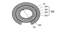
- the multilayer insulating film of the present invention has an arbitrary cross-sectional shape such as a circle, an arbitrary closed curve including an oval, etc., a triangle, a quadrangle (including a trapezoid), a polygon including a pentagon, a hexagon etc. Since the film can be deposited almost uniformly on the first surface of the first semiconductor region of the three-dimensional structure, the multilayer insulating film memory element of the following structure can be provided. Note that FIG. 2 is an example in which the multilayer insulating film configuration described in (2) is applied, and 204 is a second silicon nitride film. (6) The multilayer insulating film storage element according to (1) or (2), wherein the first semiconductor region has a three-dimensional structure of an arbitrary cross-sectional shape such as a closed curve or a polygon.
- the transistor which controls the current flowing between the second and third conductive electrodes by the potential of the first conductive electrode is: (7) The multilayer insulation according to (1) or (2), wherein the second conductive electrode and the third conductive electrode are provided in contact with the first surface with the first conductive electrode interposed therebetween. Film storage element.
- the second conductive electrode and the third conductive electrode have a rectifying junction with the first semiconductor region. When the semiconductor region is a thin film, it may have an ohmic junction.
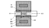
- FIG. 3 is a plan view showing this structural example, wherein 100 is a first semiconductor region (indicated by vertical hatching in FIG. 3), 200 is a multilayer insulating film, and 10 is a first conductive electrode. 20 is a second conductive electrode provided in contact with the first surface, 30 is a third conductive electrode provided in contact with the first surface, and 302 and 303 are passivations provided on the first surface as needed. Insulating film.
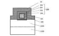
- FIG. 4 shows an example of a cross-sectional view taken along the alternate long and short dash line X1-X2 (corresponding to the channel portion of the transistor) passing over the first conductive electrode in FIG. 3, 101 is a first surface, 1100 is a support substrate, 1200 is an insulating film provided on the support substrate.
- the multilayer insulating film 200 includes four layers of a first aluminum oxide film 201, a first silicon nitride film 202, a second aluminum oxide film 203, and a second silicon nitride film 204.
- FIG. 4 shows an example in which the first surface covered by the first conductive electrode has a three-dimensional structure, and has a portion (X1-X2 cross section) in which the first semiconductor region 100 is provided floating from the support substrate,
- the multilayer insulating film 200 is formed not only on the main surface (upper surface in the case of illustration) of the first surface but also on the side surface adjacent to the main surface and the surface (bottom surface in the case of illustration) opposite to the main surface.
- the first conductive electrode can be attached to the multilayer insulating film 200 continuously from the main surface (upper surface in FIG. 4) to the lower portion of the side surface adjacent to at least the main surface (upper surface in the case shown).
- the device to which the present invention is applied is, of course, applicable to a device having a so-called planar structure in which the thickness of the first semiconductor region is very small compared to the dimension of the main surface (upper surface in the drawing).
- the first conductivity is formed on the first surface;
- the fourth conductive electrode and the second semiconductor region, and the fifth conductive electrode and the third semiconductor region have an ohmic junction.
- the second and third semiconductor regions are not in contact with the first conductive electrode.
- the positional relationship between the second semiconductor region and the third semiconductor region is the same as 302 and 303 in FIG.
- This structural example is shown in a plan view in FIG.
- reference numeral 400 denotes a second semiconductor region
- 500 denotes a third semiconductor region
- 40 denotes a fourth conductive electrode bonded to the second semiconductor region
- 50 denotes a fifth conductive electrode bonded to the third semiconductor region.
- the second semiconductor region extends to one end of the first conductive electrode
- the third semiconductor region extends to the other end of the first conductive electrode, but each is insulated from the first conductive electrode.
- the first semiconductor region is silicon, but the first semiconductor region is a compound semiconductor such as Al x Ga y As, GaAs, In x Ga y As, or a semiconductor containing Ge such as Ge or SiGe. It is valid.
- a manufacturing process of a temperature (for example, 500 ° C. or less) which the wiring layer can withstand is required. Can be produced at a temperature of 500 ° C. or less, which makes it possible to realize this stacked structure, and enables high performance and high performance of an LSI system by stacking logic and memory.
- a temperature for example, 500 ° C. or less
- the storage element of the present invention can be applied to an element of several tens of nm or less in nm size, and further to an element having a three-dimensional structure It can be used for next-generation information processing chips to realize even higher functionality and performance.
- FIG. 4 is a cross-sectional view of the case where the channel portion of the field effect transistor of FIG. 3 has a three-dimensional structure. It is a figure showing CV hysteresis curve of Example 1 of the present invention. It is a figure showing the relationship between the 1st aluminum oxide film thickness of the Example group of this invention, and the program voltage Vprg1 for obtaining a 1 V memory window.
- FIG. 6 is a diagram showing a CV hysteresis curve when heat treatment is applied to one embodiment of the present invention.
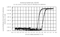
- FIG. 6 is a diagram showing a memory window obtained when the present invention is applied to a three-dimensional structure transistor.
- FIG. 4 is a plan view of an embodiment in which second and third semiconductor regions are provided in the field effect transistor of FIG. 3;
- a single crystal silicon substrate having p-type, 10 ⁇ cm, (100) plane was used.
- degreasing washing, piranha washing or nitric acid immersion, deionized water running water washing, dilute buffered hydrofluoric acid dip, deionized water running water washing, and drying were performed.
- the first aluminum oxide film is formed on the atomic layer by alternately flowing a gaseous aluminum source (here, trimethylaluminum) and an oxidant (here, plasma activated oxygen) on a heated silicon substrate in a vacuum chamber.
- a gaseous aluminum source here, trimethylaluminum
- an oxidant here, plasma activated oxygen
- the film was deposited on a silicon substrate by a method of depositing a film of close film thickness. This method is known as ALD (atomic layer deposition).
- ALD atomic layer deposition
- the first silicon nitride film is continuously formed, in the same vacuum chamber, on a heated silicon substrate, a gaseous silicon source (organic silicon, tri-dimethylaminosilane (TDMAS)) and a nitriding agent (plasma activated nitrogen). It was deposited on the first aluminum oxide film on the silicon substrate by an alternating flow method.
- TDMAS tri-dimethylaminosilane
- the second aluminum oxide film was continuously deposited on the first silicon nitride in the same manner as the first aluminum oxide film.
- the second silicon nitride film was continuously deposited on the second aluminum oxide film in the same manner as the first silicon nitride film.
- the heating temperature of the silicon substrate at the time of deposition was 250.degree.
- an aluminum electrode was mask-deposited as a first conductive electrode on the laminated multilayer insulating film.
- the multilayer films were deposited in various film thickness combinations.
- the thickness of the first aluminum oxide film is 1.5 to 5 nm
- the thickness of the second aluminum oxide film is 5 to 20 nm
- the thickness of the first silicon nitride film is 3 to 5 nm
- the thickness of the second silicon nitride film is 1.5 to 2 nm. chosen.
- FIG. 5 is a CV characteristic group of one embodiment of the multilayer insulating film storage element having the planar structure of FIG. 1 created.
- the thickness of the first aluminum oxide film was 2 nm
- the thickness of the first silicon nitride film was 3 nm
- the thickness of the second aluminum oxide film was 10 nm
- the deposited aluminum film was used as the first conductive electrode.
- the voltage between the first conductive electrode of the element and the first semiconductor region (in this case, the semiconductor substrate) is ⁇ 5 V ⁇ + 5 V ⁇ ⁇ 5 V, ⁇ 6 V ⁇ + 6 V ⁇ -6 V, ⁇ 7 V ⁇ + 7 V ⁇ -7 V, ⁇ 8 V ⁇
- the innermost hysteresis curve corresponds to -5V to + 5V to -5V sweep, and the outermost hysteresis curve corresponds to -9V to + 9V to -9V.
- ⁇ Vw is a so-called memory window.
- Vprg is changed, a plurality of CV hysteresis curves as shown in FIG. 5 are measured, and Vprg for setting the memory window ⁇ Vw to 1 V is applied to the plurality of multilayer insulating film storage elements having the plurality of film thickness combinations created above. Derived. The results for selected elements are shown in FIG. In FIG. 6, the horizontal axis is plotted as the first aluminum oxide film thickness.
- the thickness of the first aluminum oxide film is in the range of 1.5 nm to 5 nm, and the voltage Vprg1 required for programming is 4 V to 12 V, and the voltage value range of the conventional nonvolatile memory (for example, NAND flash memory It has been shown that high voltages above 17 V) are not necessary.
- the extrapolated value Vprg1 obtained by increasing the thickness of the second aluminum oxide film to 20 nm is also in the range of the voltage value of the conventional nonvolatile memory.
- FIG. 7 is a CV characteristic group after heat treatment of the element of the embodiment whose CV characteristic is shown in FIG. 5 at 350 ° C. for 30 minutes.
- the display method is set to the same as in FIG.
- the qualitative difference from Fig. 5 is the sweep curve of -9 V ⁇ +9 V ⁇ -9 V, where the area of the difference between the measurement frequencies 1 kHz and 100 KHz (shaded area) is less than half the difference partial area without heat treatment.
- the interface state density is improved to 1 ⁇ 2 or less by the heat treatment at 350 ° C. by the observation fact that the slope of the large portion of the CV curve is approximately doubled by the heat treatment. I understand.
- the heat treatment temperature is 400.degree. C.
- the area of the difference between the measurement frequency 1 kHz and 100 KHz is 1/4 to 1/5 when heat treatment is not performed, and becomes smaller by one digit when the heat treatment temperature is 450.degree.
- the heat treatment atmosphere is carried out with nitrogen and argon gas containing hydrogen at a detonation limit of 5% or less for safety, but an atmosphere with 100% hydrogen is also effective.
- the present invention since the first silicon nitride film contains hydrogen, the present invention is effective even in the atmosphere of an inert gas such as nitrogen, argon or helium which does not contain hydrogen.
- a multi-layer insulating film of the present invention was laminated on the surface of a single-crystal silicon (first semiconductor region) of a fine three-dimensional structure having a square cross section of about 25 nm on a side, and a field effect transistor using the first conductive electrode as a gate was fabricated.
- This transistor has a planar structure similar to that of FIG. 3 and a cross section similar to that of FIG.
- the laminated multi-layer insulating film has a first aluminum oxide film thickness of 2 nm, a first silicon nitride film thickness of 3 nm, a second aluminum oxide film thickness of 10 nm, and a second silicon nitride film thickness of 1.5 nm.
- the first conductive electrode is adhered to the multilayer insulating film on the surface (bottom surface in the case of FIG. 4) opposed to the main surface (upper surface in the case of FIG.
- the Id-Vg characteristics were not affected by the potential of the support substrate 1100 underlying the fine three-dimensional structure.
- the distance from the supporting substrate 1100 where the first conductive electrode adhering to the lower side of the side surface adjacent to the main surface is lower than the supporting substrate 1100 to the surface (bottom surface in the case of FIG. 4) of the first semiconductor region
- the potential of the surface (bottom surface in the case of FIG. 4) near the main surface is also mainly controlled from the first conductive electrode.
- the current flowing between the second electrode and the third electrode is controlled by the potential of the first electrode to 1E-14A or less of the measurement limit of the measurement system.
- the memory element can be mounted at low temperature on the multilayer wiring of LSI, it is possible to give flexibility to signal processing and to speed up. The advancement of electronic devices is promoted. Furthermore, since the present invention can be applied to an element having a size of several tens of nm or less, it can be used for enhancing the functions of a future nm-size LSI. In addition, according to the low temperature technology of the present invention, a control and memory function can be mounted on a display circuit or a sensor circuit on a glass substrate or an organic flexible substrate.
Landscapes
- Non-Volatile Memory (AREA)
- Semiconductor Memories (AREA)
Abstract
従来のMONOSメモリのような多層絶縁膜メモリの材料構成、製造方法は、LSIの配線層の上にメモリ素子を集積するようなたとえば500℃以下の低温製膜工程を必要とする応用には製膜温度が高くて使用できない。微細構造、特に3次元構造の半導体素子のメモリ手段として応用する場合には半導体素子の側面および底面への均一な製膜が必要であるが不完全であった。 第1表面と第1導電形を有する第1半導体領域と、該第1表面に設けられた少なくとも第1酸化アルミニュウム膜、第1窒化シリコン膜、第2酸化アルミニュウム膜を積層した多層絶縁膜と、該多層絶縁膜上に設けた第1導電電極とから少なくとも構成されることを特徴とする多層絶縁膜記憶素子を提供する。
Description
本発明は、ゲート絶縁膜に多層絶縁膜構造を用いた記憶素子、または、さらに微細構造、低温製造技術に適した記憶素子に関する。
多層絶縁膜記憶素子のカテゴリの中で、早期にメモリカードまで高集積かつ実用レベルの応用がなされたのはMONOS素子であった(非特許文献1、特許文献1)。
このMONOS素子は、半導体S(非特許文献1の場合はシリコン)上にO(第1酸化シリコン膜)\N(窒化シリコン膜)\O(第2酸化シリコン膜)を積層した多層絶縁膜を記憶手段として設けていた。なお、Mは導電電極である。
このMONOS素子は、半導体S(非特許文献1の場合はシリコン)上にO(第1酸化シリコン膜)\N(窒化シリコン膜)\O(第2酸化シリコン膜)を積層した多層絶縁膜を記憶手段として設けていた。なお、Mは導電電極である。
第1酸化シリコン膜の膜厚は、トンネル現象(direct tunneling または FN tunneling)により電子、正孔(以後総称してキャリアと呼ぶ場合がある)が該第1酸化シリコン膜を通過する程度に薄いことが必要であり、そのため均一で欠陥の少ない、しかもキャリア捕獲準位の少ない膜が不可欠であった。これを実現する製造技術としては希釈酸素雰囲気中での熱酸化が用いられていた。この熱酸化工程は、低温だと上記の要求を満たす酸化シリコン膜は得難く、800℃以上の温度を必要とした。また、窒化シリコン膜の製造工程も再現性、信頼性の優れた、凹凸の少ない薄膜を得るには690℃以上の熱CVD工程を必要とした。
酸化シリコンの低温製膜技術として、TEOSCVD(オゾンとテトラエトキシシラン(tetraethoxysilane)を原料としたCVD)、プラズマCVDが知られているが、発明者の知る限りでは、上記熱酸化品質の薄膜は得られない。
酸化シリコンの低温製膜技術として、TEOSCVD(オゾンとテトラエトキシシラン(tetraethoxysilane)を原料としたCVD)、プラズマCVDが知られているが、発明者の知る限りでは、上記熱酸化品質の薄膜は得られない。
T.Nozaki et al.,"A 1Mbit EEPROM with MONOS memory cell for semiconductor disk application",session10-4, Symposium on VLSI Circuit, 1990.
上記の従来の材料構成、製造方法は、500℃以下の熱工程が必要な、たとえばLSIの配線層の上にメモリ素子を集積するような低温製膜工程を必要とする応用には製膜温度が高くて使用できない。微細構造、特に3次元構造の半導体素子のメモリ手段として応用する場合には、半導体素子の側面および底面への均一な製膜が必要であるが、TEOSCVDやプラズマCVDで、たとえ良質の酸化シリコン膜が形成できたとしても、3次元構造のすべての面にほぼ均一な成膜は不可能であった。
上記課題を解決するために本発明では、
1)半導体表面に接触する第1酸化シリコン膜に代えて第1酸化アルミニュウム膜(AlOx、x=1~1.5)を使う。第1酸化アルミニュウム膜はnmレベルの膜厚でも均一に350℃以下の低温で製膜できることを確認し、
2)また、シリコン半導体上に製膜した第1酸化アルミニュウム膜は単一膜で、膜厚が厚い(10nm以上)時はキャリアトラップ特性が顕著に観測されるが、膜厚が5nm以下と薄くなるとキャリアトラッピングは少なくなり、かつ、その上に窒化シリコン膜を堆積した場合は、第1酸化アルミニュウム膜のトラップへのパッシベーション効果があり、従来使えないと判断されていたのに反して、多層絶縁膜記憶素子の酸化シリコン膜1(トンネル酸化シリコン膜)の代わりに使用できることを見出し、
3)さらに、上記堆積した第1酸化アルミニュウム膜を300℃~450℃で熱処理することにより、半導体表面と酸化アルミニュウム界面に存在する界面準位密度を減少させることができることを見出し、
500℃以下の低温工程で、3次元構造の素子にも適用可能な多層絶縁膜記憶素子技術を提供する。以下にその構成、製造工程を示す。
1)半導体表面に接触する第1酸化シリコン膜に代えて第1酸化アルミニュウム膜(AlOx、x=1~1.5)を使う。第1酸化アルミニュウム膜はnmレベルの膜厚でも均一に350℃以下の低温で製膜できることを確認し、
2)また、シリコン半導体上に製膜した第1酸化アルミニュウム膜は単一膜で、膜厚が厚い(10nm以上)時はキャリアトラップ特性が顕著に観測されるが、膜厚が5nm以下と薄くなるとキャリアトラッピングは少なくなり、かつ、その上に窒化シリコン膜を堆積した場合は、第1酸化アルミニュウム膜のトラップへのパッシベーション効果があり、従来使えないと判断されていたのに反して、多層絶縁膜記憶素子の酸化シリコン膜1(トンネル酸化シリコン膜)の代わりに使用できることを見出し、
3)さらに、上記堆積した第1酸化アルミニュウム膜を300℃~450℃で熱処理することにより、半導体表面と酸化アルミニュウム界面に存在する界面準位密度を減少させることができることを見出し、
500℃以下の低温工程で、3次元構造の素子にも適用可能な多層絶縁膜記憶素子技術を提供する。以下にその構成、製造工程を示す。
提供される第1の構成は、図1にその断面図を示すように、
(1)第1表面と第1導電形を有する第1半導体領域と
該第1表面に設けられた少なくとも第1酸化アルミニュウム膜、第1窒化シリコン膜、第2酸化アルミニュウム膜を積層した多層絶縁膜と、該多層絶縁膜上に設けた第1導電電極とから少なくとも構成される多層絶縁膜記憶素子。
なお、図1で、100は第1半導体領域、101は第1表面、200は多層絶縁膜、201は第1酸化アルミニュウム膜、202は第1窒化シリコン膜、203は第2酸化アルミニュウム膜、10は第1導電電極である。
(1)第1表面と第1導電形を有する第1半導体領域と
該第1表面に設けられた少なくとも第1酸化アルミニュウム膜、第1窒化シリコン膜、第2酸化アルミニュウム膜を積層した多層絶縁膜と、該多層絶縁膜上に設けた第1導電電極とから少なくとも構成される多層絶縁膜記憶素子。
なお、図1で、100は第1半導体領域、101は第1表面、200は多層絶縁膜、201は第1酸化アルミニュウム膜、202は第1窒化シリコン膜、203は第2酸化アルミニュウム膜、10は第1導電電極である。
第2酸化アルミニュウム膜のパッシベーション、またはフォトレジスト工程でのレジスト剥離改善のために更に第2窒化シリコン膜を積層した第2の構成を提供する。
(2)該第2酸化アルミニュウム膜上に更に第2窒化シリコン膜を積層したことを特徴とする(1)記載の多層絶縁膜記憶素子。
(2)該第2酸化アルミニュウム膜上に更に第2窒化シリコン膜を積層したことを特徴とする(1)記載の多層絶縁膜記憶素子。
記憶素子として従来のフラッシュメモリのプログラム電圧17V以下で動作するための望ましい第1酸化アルミニュウム膜の膜厚は下記のようになる。
(3)該第1酸化アルミニュウム膜の膜厚が1.5nm~5nmであることを特徴とする(1)、(2)記載の多層絶縁膜記憶素子。
(3)該第1酸化アルミニュウム膜の膜厚が1.5nm~5nmであることを特徴とする(1)、(2)記載の多層絶縁膜記憶素子。
該第2窒化シリコン膜が多層絶縁膜の電気特性に大きな影響を与えない膜厚は下記のようになる。
(4)該第2窒化シリコン膜厚は1.5~2nmであることを特徴とする(1)、(2)記載の多層絶縁膜記憶素子。
(4)該第2窒化シリコン膜厚は1.5~2nmであることを特徴とする(1)、(2)記載の多層絶縁膜記憶素子。
本発明の多層絶縁膜記憶素子は、第1酸化アルミニュウム膜堆積後、または多層絶縁膜積層後300℃~450℃で熱処理を行うと第1酸化アルミニュウム膜と第1半導体領域界面の界面準位密度が大幅に減少し、周波数による電気特性の変化が改善された。本発明ではこの技術を提供する。すなわち、
(5)該第1酸化アルミニュウム膜堆積後、または、さらに第1窒化シリコン膜、第2酸化アルミニュウム膜堆積後、またはさらに第2窒化シリコン膜を堆積後、300℃から450℃の温度で熱処理を行った(1)または(2)記載の多層絶縁膜記憶素子の製造方法。
熱処理の雰囲気は安全のため水素を爆発限界5%以下含む窒素、アルゴンガスで行われるが、水素100%の雰囲気でも、水素を含まない窒素、アルゴン、ヘリウムなどの不活性ガス雰囲気でも効果がある。
(5)該第1酸化アルミニュウム膜堆積後、または、さらに第1窒化シリコン膜、第2酸化アルミニュウム膜堆積後、またはさらに第2窒化シリコン膜を堆積後、300℃から450℃の温度で熱処理を行った(1)または(2)記載の多層絶縁膜記憶素子の製造方法。
熱処理の雰囲気は安全のため水素を爆発限界5%以下含む窒素、アルゴンガスで行われるが、水素100%の雰囲気でも、水素を含まない窒素、アルゴン、ヘリウムなどの不活性ガス雰囲気でも効果がある。
本発明の多層絶縁膜は図2に例示するような円形、長円形などを含む任意閉曲線、三角形、四角形(含む台形)、5角形、6角形等を含む多角形、など任意の断面形状を有する三次元構造の第1半導体領域の第1表面にほぼ一様に製膜することが可能であるので下記の構造の多層絶縁膜メモリ素子を提供できる。なお、図2は(2)記載の多層絶縁膜構成を適用した例で204は第2窒化シリコン膜である。
(6)該第1半導体領域は、閉曲線、多角形などの任意断面形状の3次元構造を有することを特徴とする(1)または(2)記載の多層絶縁膜記憶素子。
(6)該第1半導体領域は、閉曲線、多角形などの任意断面形状の3次元構造を有することを特徴とする(1)または(2)記載の多層絶縁膜記憶素子。
該第1導電電極の電位により、第2、第3導電電極間に流れる電流を制御するトランジスタは、
(7)前記第1導電電極を間に挟み離間して第2導電電極、第3導電電極を前記第1表面に接して設けたことを特徴とする(1)、(2)記載の多層絶縁膜記憶素子。
該第2導電電極、該第3導電電極は該第1半導体領域に対して整流性接合を有している。該半導体領域が薄膜である場合はオーム性接合を有していてもよい。
(7)前記第1導電電極を間に挟み離間して第2導電電極、第3導電電極を前記第1表面に接して設けたことを特徴とする(1)、(2)記載の多層絶縁膜記憶素子。
該第2導電電極、該第3導電電極は該第1半導体領域に対して整流性接合を有している。該半導体領域が薄膜である場合はオーム性接合を有していてもよい。
図3は、この構造例を示した平面図で、100は第1半導体領域(図3において縦斜線で示される)、200は多層絶縁膜、10は第1導電電極である。20は第1表面に接して設けられた第2導電電極、30は第1表面に接して設けられた第3導電電極であり、302、303は必要に応じて第1表面に設けられたパッシベーション用絶縁膜である。
図4は、図3において第1導電電極上を通る一点鎖線X1-X2(トランジスタのチャネル部分に相当)に沿って切り取られた断面図例を示し、101は第1表面、1100は支持基板、1200は支持基板上に設けられた絶縁膜である。多層絶縁膜200は図2の場合と同様、第1酸化アルミニュウム膜201、第1窒化シリコン膜202、第2酸化アルミニュウム膜203、第2窒化シリコン膜204の4層からなる場合を示している。
図4は、図3において第1導電電極上を通る一点鎖線X1-X2(トランジスタのチャネル部分に相当)に沿って切り取られた断面図例を示し、101は第1表面、1100は支持基板、1200は支持基板上に設けられた絶縁膜である。多層絶縁膜200は図2の場合と同様、第1酸化アルミニュウム膜201、第1窒化シリコン膜202、第2酸化アルミニュウム膜203、第2窒化シリコン膜204の4層からなる場合を示している。
図4は、第1導電電極が覆う第1表面が3次元構造を有する例を示し、第1半導体領域100が支持基板から浮いて設けられている部分(X1-X2断面)を有する場合は、第1表面の主面(図示の場合は上面)だけでなく、主面に隣接する側面、主面に対向する面(図示の場合は底面)にまで多層絶縁膜200が製膜される。第1導電電極は少なくとも該主面(図示の場合は上面)に隣接する側面の下部まで主面(図4では上面)から連続して多層絶縁膜200に接着して設けることができる。
本発明を適用する素子は、第1半導体領域の厚みが上記主面(図示では上面)寸法に比べて非常に小さい、いわゆるプレーナ構造の素子にももちろん適用できる。
本発明を適用する素子は、第1半導体領域の厚みが上記主面(図示では上面)寸法に比べて非常に小さい、いわゆるプレーナ構造の素子にももちろん適用できる。
該第1導電形と逆のキャリアのチャネル電流を引き出すためには、
(8)該第1導電形と逆導電形の第2半導体領域を該第1導電電極の一方の端に至るまで第1導電電極と絶縁された状態で該第1表面に、該第1導電形と逆導電形の第3半導体領域を該第1導電電極を挟み該第2半導体領域と離間して該第1導電電極の他方の端に至るまで第1導電電極と絶縁された状態で該第1表面に設け、該第2半導体領域上に第4導電電極を、該第3半導体領域上に第5導電電極を設けたことを特徴とする(7)記載の多層絶縁膜記憶素子、が提供される。
この場合は、該第4導電電極と該第2半導体領域、および該第5導電電極と該第3半導体領域はオーム性接合を有する。ただし該第2、第3半導体領域は第1導電電極には接しない。該第2半導体領域と第3半導体領域位置関係は図3の302と303と同様である。図9にこの構造例を平面図で示した。図において400は第2半導体領域、500は第3半導体領域、40は第2半導体領域へ接着された第4導電電極、50は第3半導体領域へ接着された第5導電電極である。第2半導体領域は第1導電電極の一方の端、第3半導体領域は第1導電電極の他方の端まで延在しているが、それぞれ第1導電電極とは絶縁されている。
(8)該第1導電形と逆導電形の第2半導体領域を該第1導電電極の一方の端に至るまで第1導電電極と絶縁された状態で該第1表面に、該第1導電形と逆導電形の第3半導体領域を該第1導電電極を挟み該第2半導体領域と離間して該第1導電電極の他方の端に至るまで第1導電電極と絶縁された状態で該第1表面に設け、該第2半導体領域上に第4導電電極を、該第3半導体領域上に第5導電電極を設けたことを特徴とする(7)記載の多層絶縁膜記憶素子、が提供される。
この場合は、該第4導電電極と該第2半導体領域、および該第5導電電極と該第3半導体領域はオーム性接合を有する。ただし該第2、第3半導体領域は第1導電電極には接しない。該第2半導体領域と第3半導体領域位置関係は図3の302と303と同様である。図9にこの構造例を平面図で示した。図において400は第2半導体領域、500は第3半導体領域、40は第2半導体領域へ接着された第4導電電極、50は第3半導体領域へ接着された第5導電電極である。第2半導体領域は第1導電電極の一方の端、第3半導体領域は第1導電電極の他方の端まで延在しているが、それぞれ第1導電電極とは絶縁されている。
以下の実施例では、第1半導体領域はシリコンであるが、第1半導体領域はAlxGayAs、GaAs、InxGayAs、などの化合物半導体、Ge、SiGeなどのGeを含む半導体で有効である。
ロジックLSIの配線層の上に更にメモリなどの機能層を積層する場合は、配線層が耐える温度(たとえば500℃以下)の製造工程が必要であるが、本発明の記憶素子を製造するためには500℃以下の製造で可能であるので、この積層構造の実現を可能とし、ロジックとメモリの積層によるLSIシステムの高機能、高性能化が可能となる。また、本発明の高温を必要としない記憶素子構成を、ガラス、有機フィルムへ集積することにより、低温形成電界効果素子による電子回路、ディスプレイ、センサなどの製造を行うことが出来る。
しかも酸化アルミニュウムは3次元構造の上面、側面、底面にもほぼ均一に堆積できるので、本発明の記憶素子は数十nm以下のnmサイズの素子、さらに3次元構造を有する素子にも適用できるので次世代の情報処理チップに活用して一層の高機能化、高性能化を実現することができる。
しかも酸化アルミニュウムは3次元構造の上面、側面、底面にもほぼ均一に堆積できるので、本発明の記憶素子は数十nm以下のnmサイズの素子、さらに3次元構造を有する素子にも適用できるので次世代の情報処理チップに活用して一層の高機能化、高性能化を実現することができる。
第1半導体領域を単結晶シリコンで実施するために、p形,10Ωcm,(100)面を有する単結晶シリコン基板を用いた。第1酸化アルミニュウム膜を堆積する前に、脱脂洗浄、ピラニア洗浄または硝酸浸漬、脱イオン水流水洗浄、稀バッファード弗酸ディップ、脱イオン水流水洗浄、乾燥を行った。
第1酸化アルミニュウム膜は、真空チャンバー内で、加熱シリコン基板上に、ガス状のアルミニュウム原料(ここではトリメチルアルミニュウム)と酸化剤(ここではプラズマ活性化酸素)を交互に流すことにより、原子層に近い膜厚の膜を堆積する方法で、シリコン基板上に堆積した。この方法はALD(atomic layer deposition )として知られている。
第1窒化シリコン膜は連続して、同一真空チャンバー内で、加熱シリコン基板上に、ガス状のシリコン原料(有機シリコン、トリ・ディメチルアミノシラン(TDMAS))と窒化剤(プラズマ活性窒素)とを交互に流す方法で、シリコン基板上の第1酸化アルミニュウム膜上に堆積した。
第2酸化アルミニュウム膜は、第1酸化アルミニュウム膜と同様な方法で第1窒化シリコン上へ連続して堆積した。
第2窒化シリコン膜が必要な場合は、第1窒化シリコン膜と同様な方法で連続して第2酸化アルミニュウム膜上に堆積した。
堆積時のシリコン基板の加熱温度は250℃とした。
第1窒化シリコン膜は連続して、同一真空チャンバー内で、加熱シリコン基板上に、ガス状のシリコン原料(有機シリコン、トリ・ディメチルアミノシラン(TDMAS))と窒化剤(プラズマ活性窒素)とを交互に流す方法で、シリコン基板上の第1酸化アルミニュウム膜上に堆積した。
第2酸化アルミニュウム膜は、第1酸化アルミニュウム膜と同様な方法で第1窒化シリコン上へ連続して堆積した。
第2窒化シリコン膜が必要な場合は、第1窒化シリコン膜と同様な方法で連続して第2酸化アルミニュウム膜上に堆積した。
堆積時のシリコン基板の加熱温度は250℃とした。
ついで、上記積層した多層絶縁膜の上へ第1導電電極としてアルミニュウム電極をマスク蒸着した。
上記多層膜は各種膜厚の組み合わせで堆積された。第1酸化アルミニュウム膜厚は1.5~5nm、第2酸化アルミニュウム膜厚は5~20nm、第1窒化シリコン膜厚は3~5nm、第2窒化シリコン膜厚は1.5~2nmの範囲から選択された。
その結果、作成された多層絶縁膜記憶素子のIV特性、CV特性を評価した。
その結果、作成された多層絶縁膜記憶素子のIV特性、CV特性を評価した。
図5は、作成された図1の平面構造を有する多層絶縁膜記憶素子の1実施例のCV特性群である。第1酸化アルミニュウム膜厚を2nm、第1窒化シリコン膜厚を3nm、第2酸化アルミニュウム膜厚を10nmとし、蒸着アルミニュウム膜を第1導電電極とした。素子の第1導電電極と第1半導体領域(この場合は半導体基板)間の電圧を、-5V→+5V→-5V、-6V→+6V→-6V、-7V→+7V→-7V、-8V→+8V→-8V、-9V→+9V→-9Vと掃印(スイープ)して測定したCVヒステリシス曲線を重ねて表示した図である。一番内側のヒステリシス曲線は、-5V→+5V→-5Vスイープ対応、一番外側のヒステリシス曲線は-9V→+9V→-9V対応である。曲線群全体で電気容量(capacitance)の測定周波数が1KHzの場合を示してあるが、-9V→+9V→-9V対応ヒステリシス曲線のみ1KHzと100KHzの両方が示されている。
スイープ電圧の負側端をVprg-、正側端をVprg+と表記し、Vprg-からVprg+へスイープしたときに得られるCV曲線のC=Cmax/2に対応する電圧をVw-、Vprg+からVprg-へスイープしたときに得られるCV曲線のC=Cmax/2に対応する電圧をVw+、とし、ΔVw=Vw+ - Vw-と定義する。ΔVwはいわゆるメモリウィンドウ(memory window)となる。スイープ電圧の両端の絶対値が等しいときは、+-を付記しないVprgと記す。
上記作成された複数の膜厚組み合わせを有する複数の多層絶縁膜記憶素子について、Vprgを変化させ、図5のような多数のCVヒステリシス曲線を測定し、メモリウィンドウΔVwを1VとするためのVprgを導出した。選択された素子についての結果を図6に示す。図6は横軸を第1酸化アルミニュウム膜厚としてプロットされている。
第1酸化アルミニュウム膜厚が1.5nm~5nmの範囲ではメモリ特性が示され、プログラムに必要な電圧Vprg1は4V~12Vであり、従来の不揮発性メモリの電圧値の範囲(たとえばNANDフラッシュメモリの17V)を超える高電圧は不要であることが示されている。第2酸化アルミニュウム膜厚を20nmまで大きくした外挿値のVprg1も従来の不揮発性メモリの電圧値の範囲である。
図5のVprg=9Vの曲線で測定周波数1KHzの曲線と100KHzの曲線とで曲線の裾の方で差がある。この差分を斜線で示している。これは第1半導体領域表面と第1酸化アルミニュウム膜の間に界面準位が存在することを示しており、斜線の面積はその界面準位密度に比例する。この界面準位は本発明の多層絶縁膜を電界効果トランジスタのチャネル部分(第1半導体領域)上へ設け、記憶機能を有するトランジスタとして実施するときは、トランジスタ電流に雑音、短時間経時変化、ゲート閾値電圧の変動を生じさせる。
本発明では、この界面準位密度を減少させるために300℃~450℃で熱処理を行う方法をとる。
図7は、図5にCV特性を示した実施例の素子を350℃、30分熱処理した後のCV特性群である。表示の方法は図5と同じに設定されている。図5との定性的な差異は、-9V→+9V→-9Vのスイープ曲線で、測定周波数1KHzと100KHzとの差部分(斜線部分)の面積が熱処理のない差部分面積の1/2以下となっていること、及びCV曲線の勾配の大きい部分の傾きが熱処理によって約2倍にシャープになっている観測事実により界面準位密度は350℃の熱処理により1/2以下に改善されていることがわかる。
図7は、図5にCV特性を示した実施例の素子を350℃、30分熱処理した後のCV特性群である。表示の方法は図5と同じに設定されている。図5との定性的な差異は、-9V→+9V→-9Vのスイープ曲線で、測定周波数1KHzと100KHzとの差部分(斜線部分)の面積が熱処理のない差部分面積の1/2以下となっていること、及びCV曲線の勾配の大きい部分の傾きが熱処理によって約2倍にシャープになっている観測事実により界面準位密度は350℃の熱処理により1/2以下に改善されていることがわかる。
熱処理温度を400℃としたときは、測定周波数1KHzと100KHzとの差部分の面積は熱処理をしない時の1/4~1/5となり、熱処理温度450℃の時は一桁小さくなる。ただし、メモリウィンドウは熱処理温度が350℃の時約0.85倍に、400℃の時さらに0.85倍に縮減するので応用によって最適温度を選ぶ必要がある。
熱処理の雰囲気は、安全のため水素を爆発限界5%以下含む窒素、アルゴンガスで行われるが、水素100%の雰囲気でも効果はある。本発明の場合は第1窒化シリコン膜に水素が含まれているので、水素を含まない窒素、アルゴン、ヘリウムなどの不活性ガス雰囲気でも効果がある。
熱処理の雰囲気は、安全のため水素を爆発限界5%以下含む窒素、アルゴンガスで行われるが、水素100%の雰囲気でも効果はある。本発明の場合は第1窒化シリコン膜に水素が含まれているので、水素を含まない窒素、アルゴン、ヘリウムなどの不活性ガス雰囲気でも効果がある。
本発明の多層絶縁膜を一辺約25nmの四角形断面を有する微細3次元構造の単結晶シリコン(第1半導体領域)表面に積層し、第1導電電極をゲートとする電界効果トランジスタを作製した。このトランジスタは図3と同様な平面構造、図4と同様な断面を有する。積層された多層絶縁膜の構成は、第1酸化アルミニュウム膜厚が2nm、第1窒化シリコン膜厚が3nm、第2酸化アルミニュウム膜厚が10nm、第2窒化シリコン膜厚が1.5nmである。この電界効果トランジスタのドレイン電流―ゲート電圧依存性(Id-Vg特性)のメモリヒステリシス曲線を測定した結果を図8に示す。Vprg=7Vの時、ΔVw=1.9Vが得られた。図2の断面は閉曲線で示されているが本実施例の第1半導体領域の断面は図4に示されているような多角形断面の一つである。
図2、4に例示されているように本実施例では主面(図4の場合は上面)に対向する面(図4の場合は底面)には第1導電電極が該多層絶縁膜へ接着していない部分があるが、該微細3次元構造の下方にある支持基板1100の電位の影響をId-Vg特性は受けなかった。
該主面に隣接する側面下方まで接着している第1導電電極の方が下方にある支持基板1100より第1半導体領域の該主面に対向する面(図4の場合は底面)に距離が近く、該主面に対向する面(図4の場合は底面)の電位も第1導電電極から主として制御している。また、第2電極と第3電極間を流れる電流(通常の電界効果トランジスタのドレイン・ソース電流に相当)が測定システムの測定限界の1E-14A以下まで第1電極の電位で制御されている。
これら得られた特徴は、第1表面の主面(図4の場合は上面)、該主面に隣接する側面、該主面に対向する面(図4の場合は底面)にほぼ一様に本発明の多層絶縁膜が付着していることを示唆している。
本発明の技術により、LSIの多層配線の上に低温でメモリ素子が搭載できるので、信号処理にフレキシビリティを与えることができ、高速化も可能となる。電子機器の高機能化が促進される。さらに数十nm以下のnmサイズの素子にも提要できるので、将来のnmサイズのLSIの高機能化にも活用することができる。
また、本発明の低温技術により、ガラス基板、有機フレキシブル基板上のディスプレイ回路またはセンサ回路に制御、メモリ機能を搭載することができる。
また、本発明の低温技術により、ガラス基板、有機フレキシブル基板上のディスプレイ回路またはセンサ回路に制御、メモリ機能を搭載することができる。
10 第1導電電極
20 第2導電電極
30 第3導電電極
40 第4導電電極
50 第5導電電極
100 第1半導体領域
101 第1表面
200 多層絶縁膜
201 第1酸化アルミニュウム膜
202 第1窒化シリコン膜
203 第2酸化アルミニュウム膜
204 第2窒化シリコン膜
302、303 パッシベーション用絶縁膜
400 第2半導体領域
500 第3半導体領域
1100 支持基板
1200 絶縁膜
20 第2導電電極
30 第3導電電極
40 第4導電電極
50 第5導電電極
100 第1半導体領域
101 第1表面
200 多層絶縁膜
201 第1酸化アルミニュウム膜
202 第1窒化シリコン膜
203 第2酸化アルミニュウム膜
204 第2窒化シリコン膜
302、303 パッシベーション用絶縁膜
400 第2半導体領域
500 第3半導体領域
1100 支持基板
1200 絶縁膜
Claims (8)
- 第1表面と第1導電形を有する第1半導体領域と、
該第1表面に設けられた少なくとも第1酸化アルミニュウム膜、第1窒化シリコン膜、第2酸化アルミニュウム膜を積層した多層絶縁膜と、
該多層絶縁膜上に設けた第1導電電極とから少なくとも構成されることを特徴とする多層絶縁膜記憶素子。 - 該第2酸化アルミニュウム膜上に更に第2窒化シリコン膜を積層したことを特徴とする請求項1記載の多層絶縁膜記憶素子。
- 該第1酸化アルミニュウム膜の膜厚が1.5nm~5nmであることを特徴とする請求項1または請求項2のいずれか1項に記載の多層絶縁膜記憶素子。
- 該第2窒化シリコン膜厚は1.5~2nmであることを特徴とする請求項1または請求項2のいずれか1項に記載の多層絶縁膜記憶素子。
- 該第1酸化アルミニュウム膜堆積後、またはさらに第1窒化シリコン膜、第2酸化アルミニュウム膜堆積後、またはさらに第2窒化シリコン膜を堆積後、300℃から450℃の温度で熱処理を行うことを特徴とする請求項1または請求項2のいずれか1項に記載の多層絶縁膜記憶素子の製造方法。
- 該第1半導体領域は、閉曲線、多角形などの任意断面形状の3次元構造を有することを特徴とする請求項1または請求項2のいずれか1項に記載の多層絶縁膜記憶素子。
- 前記第1導電電極を間に挟み離間して第2導電電極、第3導電電極を前記第1表面に接して設けたことを特徴とする請求項1または請求項2のいずれか1項に記載の多層絶縁膜記憶素子。
- 該第1導電形と逆導電形の第2半導体領域を該第1導電電極の一方の端に至るまで第1導電電極と絶縁された状態で該第1表面に、該第1導電形と逆導電形の第3半導体領域を該第1導電電極を挟み該第2半導体領域と離間して該第1導電電極の他方の端に至るまで第1導電電極と絶縁された状態で該第1表面に設け、該第2半導体領域上に第4導電電極を、該第3半導体領域上に第5導電電極を設けたことを特徴とする請求項7記載の多層絶縁膜記憶素子。
Applications Claiming Priority (2)
| Application Number | Priority Date | Filing Date | Title |
|---|---|---|---|
| JP2014-262484 | 2014-12-25 | ||
| JP2014262484 | 2014-12-25 |
Publications (1)
| Publication Number | Publication Date |
|---|---|
| WO2016104637A1 true WO2016104637A1 (ja) | 2016-06-30 |
Family
ID=56150650
Family Applications (1)
| Application Number | Title | Priority Date | Filing Date |
|---|---|---|---|
| PCT/JP2015/086084 Ceased WO2016104637A1 (ja) | 2014-12-25 | 2015-12-24 | 多層絶縁膜記憶素子 |
Country Status (1)
| Country | Link |
|---|---|
| WO (1) | WO2016104637A1 (ja) |
Citations (4)
| Publication number | Priority date | Publication date | Assignee | Title |
|---|---|---|---|---|
| JP2003068892A (ja) * | 2001-08-24 | 2003-03-07 | Sony Corp | 不揮発性半導体メモリ装置の製造方法 |
| JP2009194311A (ja) * | 2008-02-18 | 2009-08-27 | Toshiba Corp | 不揮発性半導体メモリ装置およびその製造方法 |
| JP2011171771A (ja) * | 2011-06-06 | 2011-09-01 | Toshiba Corp | 不揮発性半導体メモリ |
| JP2012074633A (ja) * | 2010-09-29 | 2012-04-12 | Toshiba Corp | 半導体記憶装置 |
-
2015
- 2015-12-24 WO PCT/JP2015/086084 patent/WO2016104637A1/ja not_active Ceased
Patent Citations (4)
| Publication number | Priority date | Publication date | Assignee | Title |
|---|---|---|---|---|
| JP2003068892A (ja) * | 2001-08-24 | 2003-03-07 | Sony Corp | 不揮発性半導体メモリ装置の製造方法 |
| JP2009194311A (ja) * | 2008-02-18 | 2009-08-27 | Toshiba Corp | 不揮発性半導体メモリ装置およびその製造方法 |
| JP2012074633A (ja) * | 2010-09-29 | 2012-04-12 | Toshiba Corp | 半導体記憶装置 |
| JP2011171771A (ja) * | 2011-06-06 | 2011-09-01 | Toshiba Corp | 不揮発性半導体メモリ |
Similar Documents
| Publication | Publication Date | Title |
|---|---|---|
| KR101623961B1 (ko) | 트랜지스터와 그 제조방법 및 트랜지스터를 포함하는 전자소자 | |
| TWI570850B (zh) | 記憶體裝置及其製造方法 | |
| US20110266611A1 (en) | Nonvolatile memory device and method for fabricating the same | |
| JP2020010050A (ja) | 半導体装置 | |
| KR101603768B1 (ko) | 트랜지스터와 그 제조방법 및 트랜지스터를 포함하는 평판표시장치 | |
| KR101638977B1 (ko) | 트랜지스터와 그 제조방법 및 트랜지스터를 포함하는 전자소자 | |
| TWI769929B (zh) | 半導體元件及使用其之電氣機器 | |
| TW201212210A (en) | Semiconductor device and driving method thereof | |
| US9780228B2 (en) | Oxide semiconductor device and method for manufacturing same | |
| KR101587129B1 (ko) | 양방향성 트랜지스터 및 그 제조방법 | |
| KR20090010758A (ko) | 전하 트랩형 메모리 소자 | |
| WO2010087265A1 (ja) | 不揮発性半導体記憶装置およびその製造方法 | |
| CN102231365B (zh) | 不挥发电荷存储器件的制备方法、所得不挥发电荷存储器件及其应用 | |
| JP2015508569A (ja) | ダイヤモンドの基板にmos積層体を製造する方法 | |
| CN111989865A (zh) | 半导体装置 | |
| Chen et al. | Metal floating gate memory device with SiO 2/HfO 2 dual-layer as engineered tunneling barrier | |
| TWI515912B (zh) | 半導體元件 | |
| JPH05129630A (ja) | 不揮発性半導体記憶装置の製造方法 | |
| JP2011142246A (ja) | 半導体記憶装置 | |
| KR100905276B1 (ko) | 다층 터널 절연막을 포함하는 플래시 메모리 소자 및 그제조 방법 | |
| US20130240976A1 (en) | Nonvolatile semiconductor memory device and manufacturing method thereof | |
| TWI536505B (zh) | 不揮發性半導體記憶裝置、不揮發性半導體記憶裝置之製造方法、及製造裝置 | |
| JP2008053554A (ja) | 電子デバイスとその製造方法 | |
| JP6015992B2 (ja) | 水素化アモルファスシリコン系膜を有する記憶素子 | |
| US20100246269A1 (en) | Nonvolatile memory and methods for manufacturing the same with molecule-engineered tunneling barriers |
Legal Events
| Date | Code | Title | Description |
|---|---|---|---|
| 121 | Ep: the epo has been informed by wipo that ep was designated in this application |
Ref document number: 15873205 Country of ref document: EP Kind code of ref document: A1 |
|
| NENP | Non-entry into the national phase |
Ref country code: DE |
|
| 122 | Ep: pct application non-entry in european phase |
Ref document number: 15873205 Country of ref document: EP Kind code of ref document: A1 |
|
| NENP | Non-entry into the national phase |
Ref country code: JP |