WO2016104251A1 - セラミック素地及びその製造方法 - Google Patents
セラミック素地及びその製造方法 Download PDFInfo
- Publication number
- WO2016104251A1 WO2016104251A1 PCT/JP2015/085062 JP2015085062W WO2016104251A1 WO 2016104251 A1 WO2016104251 A1 WO 2016104251A1 JP 2015085062 W JP2015085062 W JP 2015085062W WO 2016104251 A1 WO2016104251 A1 WO 2016104251A1
- Authority
- WO
- WIPO (PCT)
- Prior art keywords
- mass
- ceramic substrate
- terms
- ceramic
- peak intensity
- Prior art date
- Legal status (The legal status is an assumption and is not a legal conclusion. Google has not performed a legal analysis and makes no representation as to the accuracy of the status listed.)
- Ceased
Links
Images

Classifications
-
- C—CHEMISTRY; METALLURGY
- C04—CEMENTS; CONCRETE; ARTIFICIAL STONE; CERAMICS; REFRACTORIES
- C04B—LIME, MAGNESIA; SLAG; CEMENTS; COMPOSITIONS THEREOF, e.g. MORTARS, CONCRETE OR LIKE BUILDING MATERIALS; ARTIFICIAL STONE; CERAMICS; REFRACTORIES; TREATMENT OF NATURAL STONE
- C04B35/00—Shaped ceramic products characterised by their composition; Ceramics compositions; Processing powders of inorganic compounds preparatory to the manufacturing of ceramic products
- C04B35/01—Shaped ceramic products characterised by their composition; Ceramics compositions; Processing powders of inorganic compounds preparatory to the manufacturing of ceramic products based on oxide ceramics
- C04B35/16—Shaped ceramic products characterised by their composition; Ceramics compositions; Processing powders of inorganic compounds preparatory to the manufacturing of ceramic products based on oxide ceramics based on silicates other than clay
- C04B35/18—Shaped ceramic products characterised by their composition; Ceramics compositions; Processing powders of inorganic compounds preparatory to the manufacturing of ceramic products based on oxide ceramics based on silicates other than clay rich in aluminium oxide
Definitions
- the present invention relates to a ceramic substrate, for example, a ceramic substrate suitable for use in a ceramic package, a high-frequency circuit board, or the like in which elements such as vibrators are mounted, and a method for manufacturing the same.
- Ceramic bodies for example, ceramic bodies (mullite bodies) mainly composed of mullite (3Al 2 O 3 .2SiO 2 ) are disclosed in JP 2010-098049 A, JP 2012-137345 A and JP 2012-138432 A.
- a ceramic substrate described in the publication No. is known.
- the multilayer ceramic substrate described in JP 2010-098049 A has a mullite content of 93 to 99% by mass of the ceramic component, and contains at least one of Mg and Y as a component other than mullite.
- the multilayer ceramic substrate contains at least one of W and Mo as a component of the conductive layer.
- Si is 1.0 to 3.0% by mass in terms of SiO 2 and Al is Al 2.
- O 3 0.4 ⁇ 1.0 wt% in terms of 1.0-4.0 parts by mass of Mn in Mn 2 O 3 in terms contains 2.0-8.0 parts by mass of Ti in terms of TiO 2.
- the mullite sintered body described in Japanese Patent Application Laid-Open No. 2012-138432 has a first region present in at least a part of the periphery of the internal wiring layer and a second region other than the first region.
- the ratio of the main peak intensity of alumina to the main peak intensity of mullite in the first region is 0.4 or more.
- the ratio of the main peak intensity of alumina to the main peak intensity of mullite in the second region is 0.3 or less.
- the Young's modulus increases as the bending strength increases.
- the Young's modulus is high, there is a problem that cracking is likely to occur because the material is difficult to deform and brittle, and chipping at the time of chip division is likely to occur.
- a ceramic substrate on which an electrode layer and a wiring layer are formed can be obtained by simultaneously firing a ceramic molded body and a metal film.
- the Young's modulus of the ceramic substrate is increased, cracks are likely to occur against bending stress in a small and low-profile package mounted on a wearable device, an IC card or the like.
- the mullite substrate has a low Young's modulus but has a low strength, it has not been applied to a ceramic package in which an element such as a vibrator is mounted inside, which requires strength.
- the techniques described in Japanese Patent Application Laid-Open No. 2010-098049, Japanese Patent Application Laid-Open No. 2012-137345 and Japanese Patent Application Laid-Open No. 2012-138432 also place importance on the dimensional accuracy and chemical resistance required for the probe card, No consideration is given to strength or Young's modulus.
- the present invention has been made in consideration of such problems, and is also suitable for a high-frequency circuit board, has a high bending strength, has a low Young's modulus, and uses a ceramic substrate (ceramic package, high-frequency). It is an object of the present invention to provide a ceramic substrate and a method for manufacturing the same, which can realize a reduction in size of a circuit board for use at a low cost.
- the ceramic substrate according to the first aspect of the present invention is characterized in that the crystal phase includes 3Al 2 O 3 .2SiO 2 as a main crystal phase and Al 2 O 3 and ZrO 2 in addition.
- the peak intensity of (113) plane in the X-ray diffraction result of the ceramic substrate containing 92% or more of Al 2 O 3 is Pa, and 3Al 2 O in the X-ray diffraction result of the ceramic substrate.
- the ratio of the peak intensity Pb to the peak intensity Pa (Pb / Pa) is preferably 5 to 50%.
- the peak intensity of the (113) plane in the X-ray diffraction result of the ceramic substrate containing 92% or more of Al 2 O 3 is Pa, and Al 2 O in the X-ray diffraction result of the ceramic substrate.
- the ratio of the peak intensity Pc to the peak intensity Pa (Pc / Pa) is preferably 5 to 25%.
- the peak intensity of the (113) plane in the X-ray diffraction result of the ceramic substrate containing 92% or more of Al 2 O 3 is Pa, and t-ZrO in the X-ray diffraction result of the ceramic substrate.
- the peak intensity of 2 (111) plane Pt when the m-ZrO 2 (/ 111) peak intensity of a peak intensity Pm1, m-ZrO 2 (111) plane of the surface Pm2, the peak intensity Pa
- the total ratio ⁇ (Pt + Pm1 + Pm2) / Pa) ⁇ of the peak intensities Pt, Pm1 and Pm2 with respect to is preferably 15 to 200%.
- Al is 40.0 to 70.0% by mass in terms of Al 2 O 3
- Zr is 5.0 to 40.0% by mass in terms of ZrO 2
- Si is in terms of SiO 2 . It is preferable to contain 10.0 to 30.0% by mass and Mn to be 2.0 to 8.0% by mass in terms of MnO.
- Ba is When it contains, it contains 1.5 mass% or less in terms of BaO, when it contains Ti, it contains 1.5 mass% or less in terms of TiO 2 , and when Y is contained, it contains 1.5 mass% in terms of Y 2 O 3.
- containing Ca it may contain 1.5 mass% or less in terms of CaO, and in the case of Mg, it may contain 1.5 mass% or less in terms of MgO.
- sintering is preferably performed at a temperature of 1200 to 1400 ° C.
- the bending strength is 450 Ma or more and the Young's modulus is 240 GPa or less.
- the bending strength is 450 MPa to 900 MPa and the Young's modulus is 170 GPa to 240 GPa.
- the dielectric loss tangent is preferably 50 ⁇ 10 ⁇ 4 or less at 1 MHz, and the relative dielectric constant is preferably 7 to 13.
- the method for producing a ceramic substrate according to the second aspect of the present invention comprises: Al is 40.0 to 70.0% by mass in terms of Al 2 O 3 , and Zr is 5.0 to 40.0% by mass in terms of ZrO 2. , A molded body preparation step of manufacturing a molded body containing 10.0 to 30.0 mass% of Si in terms of SiO 2 and 2.0 to 8.0 mass% of Mn in terms of MnO; And a firing step of firing at ⁇ 1400 ° C.
- the molded body contains at least one element of Ba, Ti, Y, Ca and Mg, and the total of Al 2 O 3 , ZrO 2 , SiO 2 and MnO.
- Ba 1.5% by mass or less in terms of BaO is included.
- Ti 1.5% by mass or less in terms of TiO 2 is included
- Y Y 2
- it may be contained in an amount of 1.5 mass% or less in terms of CaO
- in the case of containing Mg it may be contained in an amount of 1.5 mass% or less in terms of MgO.
- the method further comprises a step of forming a conductor layer containing a metal on the molded body after the molded body manufacturing step, wherein the conductor layer is formed in the firing step. May be fired.
- the firing step may be performed in a hydrogen and nitrogen forming gas containing 5% or more of hydrogen.
- the ceramic substrate and the method for manufacturing the same according to the present invention the following effects can be obtained.
- A High bending strength and low Young's modulus.
- B It is also suitable for a high frequency circuit board.
- C The chipping occurrence rate at the time of chip division is also small.
- D It is difficult to break due to bending stress when mounted as a package component or the like.
- E It is difficult for cracks to occur during brazing.
- F Yield can be improved, and downsizing of products (ceramic package, high frequency circuit board, etc.) using a ceramic substrate can be realized at low cost.
- G For low-temperature firing, a low-resistance conductor such as Cu (copper) -W (tungsten) can be used as an electrode or wiring.
- ⁇ indicating a numerical range is used as a meaning including numerical values described before and after the numerical value as a lower limit value and an upper limit value.
- the crystal phase includes 3Al 2 O 3 .2SiO 2 as a main crystal phase, and additionally includes Al 2 O 3 and ZrO 2 .
- the peak intensity of the (113) plane in the X-ray diffraction results of the ceramic substrate containing 92% or more of Al 2 O 3 is Pa
- the ratio of the peak intensity Pb to the peak intensity Pa (Pb / Pa) is preferably 5 to 50%.
- the ratio of the peak intensity Pc to the peak intensity Pa is 5 to It is preferably 25%.
- the ratio ⁇ (Pt + Pm1 + Pm2) / Pa) ⁇ of the sum of the peak intensities Pt, Pm1 and Pm2 to the peak intensity Pa is preferably 15 to 200%.
- Al is 40.0 to 70.0% by mass in terms of Al 2 O 3
- Zr is 5.0 to 40.0% by mass in terms of ZrO 2
- Si is 10.0 to 30 in terms of SiO 2. It is preferable that 0.0 mass% and Mn is contained in an amount of 2.0 to 8.0 mass% in terms of MnO.
- At least one element of Ba, Ti, Y, Ca, and Mg may be included.
- the total of Al 2 O 3 , ZrO 2 , SiO 2 and MnO is 100% by mass
- when Ba is included 1.5% by mass or less in terms of BaO is included
- when Ti is included 1 in terms of TiO 2 It includes .5 wt% or less
- it contains Ca comprises 1.5 wt% or less in terms of CaO
- a bending strength of 450 Ma or more and a Young's modulus of 240 GPa or less can be realized. More specifically, it is possible to realize a bending strength of 450 MPa to 900 MPa and a Young's modulus of 170 GPa to 240 GPa.
- the “bending strength” refers to a four-point bending strength, which is a value measured at room temperature based on JIS R1601 (bending test method for fine ceramics).
- the dielectric loss tangent can be 50 ⁇ 10 ⁇ 4 or less and the relative dielectric constant of 7 to 13 at 1 MHz.
- this ceramic substrate is made of 3Al 2 O 3 .2SiO 2 (mullite) powder of 50 to 93 mass%, ZrO 2 powder of 5 to 40 mass%, Al 2 O 3 powder of 0 to 36 mass%, and SiO 2 powder.
- the molded body is fired at 1200 to 1400 ° C.
- the average particle size of 3Al 2 O 3 .2SiO 2 powder is 0.5 to 4.0 ⁇ m
- the average particle size of ZrO 2 powder is 0.05 to 1.0 ⁇ m
- the average particle size of Al 2 O 3 powder is 0.3
- the average particle size of the SiO 2 powder is 0.1 to 2.5 ⁇ m
- the average particle size of the MnO powder is 0.5 to 4.0 ⁇ m.
- the additive include at least one powder among BaO powder, TiO 2 powder, Y 2 O 3 powder, CaO powder, and MgO powder.
- the amount of the additive when the total of the Al 2 O 3 powder, the ZrO 2 powder, the SiO 2 powder and the MnO powder is 100% by mass, it is preferable that at least one kind of powder is contained by 1.5% by mass or less.
- the average particle size of the BaO powder is 0.5 to 4.0 ⁇ m
- the average particle size of the TiO 2 powder is 0.05 to 1.0 ⁇ m
- the average particle size of the Y 2 O 3 powder is 0.1 to 5.0 ⁇ m
- CaO The average particle size of the powder is preferably 0.5 to 2.0 ⁇ m
- the average particle size of the MgO powder is preferably 0.1 to 1.0 ⁇ m.
- the average particle size of the raw material is 50% of the passage size from the small particle size side (cumulative passage rate) in the volume-based particle size distribution obtained by laser diffraction scattering type particle size distribution measurement method (LA-920, manufactured by HORIBA). % Particle size.
- the strength of a ceramic substrate mainly composed of mullite (3Al 2 O 3 .2SiO 2 ) having a low Young's modulus can be improved.
- the silica component of mullite can be extracted with an additive, and thereby the alumina (Al 2 O 3 ) can be precipitated to increase the strength.
- the Young's modulus and strength can be controlled by adjusting the amount of the additive and increasing or decreasing the amount of precipitation of alumina.
- the ceramic substrate according to the present embodiment can be sintered at a low temperature of 1200 to 1400 ° C., and a ceramic substrate having a bending strength of 450 MPa or more and a Young's modulus of 240 GPa or less can be realized. . Specifically, a ceramic substrate having a bending strength of 450 MPa to 900 MPa and a Young's modulus of 170 GPa to 240 GPa can be realized.
- the Young's modulus increases as the bending strength increases.
- the Young's modulus is high, there is a problem that cracking is likely to occur because the material is difficult to deform and brittle, and chipping at the time of chip division is likely to occur.
- the ceramic substrate according to the present embodiment is also suitable for a high-frequency circuit board, and even if the bending strength is 450 MPa or more, the Young's modulus is as low as 240 GPa, so the chipping occurrence rate at the time of chip division is Small, difficult to break due to bending stress when mounted as a package component, etc., cracks are difficult to occur when brazing, can improve yield, ceramic products (ceramic package, high frequency circuit) Substrate etc. can be downsized at low cost.
- the bending strength can be easily improved and the Young's modulus can be suppressed from increasing, and the dielectric constant can be increased. And a decrease in thermal conductivity can be suppressed.
- the Si content By setting the Si content to 10.0 to 30.0 mass% in terms of SiO 2 , it is possible to suppress a decrease in the amount of the generated glass phase, and it is easy to achieve densification at 1200 to 1400 ° C. Moreover, the fall of the softening temperature of the glass produced
- the Mn content By setting the Mn content to 2.0 to 8.0% by mass in terms of MnO, it is possible to suppress a decrease in the amount of the generated glass phase, and it becomes easy to achieve densification at 1200 to 1400 ° C. Moreover, the fall of the softening temperature of the glass produced
- the firing temperature of the porcelain can be optimized, the strength of the glass phase produced can be increased, and the ceramic substrate containing mullite with a low Young's modulus
- the bending strength of can be improved.
- it can be produced at a low firing temperature, which is advantageous for cost reduction.
- the chipping occurrence rate in chip division by the pressing roller can be reduced, and productivity can be improved.
- Electrical characteristics (dielectric loss tangent) can also be kept low, which is preferable for use in, for example, high-frequency circuit boards.
- a low-resistance conductor such as Cu (copper) -W (tungsten) can be used as the electrode and wiring.
- the low resistance means that the surface resistance with a thickness of 15 ⁇ m is 10 m ⁇ / sq. It means the following.
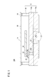
- the ceramic package according to the first configuration example (hereinafter referred to as the first package 10A) is similar to the multilayer substrate 12 configured with the ceramic substrate according to the present embodiment. And a lid body 14 made of a ceramic body according to the embodiment.
- the laminated substrate 12 is configured by laminating at least a plate-like first substrate 16a, a plate-like second substrate 16b, and a frame 18 in this order.
- the laminated substrate 12 includes an upper surface electrode 20 formed on the upper surface of the second substrate 16b, a lower surface electrode 22 formed on the lower surface of the first substrate 16a, an inner layer electrode 24 formed inside, and the inner layer.
- a first via hole 26a that electrically connects the electrode 24 and the lower surface electrode 22 and a second via hole 26b that electrically connects the inner layer electrode 24 and the upper surface electrode 20 are provided.
- a crystal resonator 30 is electrically connected to the upper surface electrode 20 via a conductor layer 32 in an accommodation space 28 surrounded by the upper surface of the second substrate 16b and the frame body 18. Yes. Further, in order to protect the crystal unit 30, the lid 14 is hermetically sealed on the upper surface of the frame 18 through the glass layer 34.
- the crystal resonator 30 is mounted in the accommodation space 28 , but in addition, at least one or more of resistors, filters, capacitors, and semiconductor elements may be mounted. Good.
- the dielectric loss tangent is 50 ⁇ 10 ⁇ 4 or less and the relative dielectric constant is 7 to 13 at 1 MHz, which is suitable as a high-frequency circuit board.
- the bending strength is 450 MPa or more and the Young's modulus is 240 GPa or less.
- the “bending strength” refers to a four-point bending strength, which is a value measured at room temperature based on JIS R1601 (bending test method for fine ceramics).
- the ceramic substrate according to the present embodiment has the above-described composition, it can be sintered at a low temperature of 1200 to 1400 ° C. Therefore, the precursor of the ceramic base (molded body before firing), the electrodes (upper surface electrode 20, lower surface electrode 22, inner layer electrode 24) and via hole 26 (first via hole 26a, second via hole 26b) are simultaneously fired. Thus, the laminated substrate 12 can be manufactured, and the manufacturing process can be simplified.
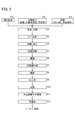
- step S1a of FIG. 2 3Al 2 O 3 .2SiO 2 (mullite) powder is 50 to 93 mass%, ZrO 2 powder is 5 to 40 mass%, Al 2 O 3 powder is 0 to 36 mass%, SiO 2 2 A mixed powder containing 0 to 16% by mass of powder and 2 to 8% by mass of MnO powder is prepared, an organic component (binder) is prepared in step S1b, and a solvent is prepared in step S1c.
- the average particle size of the 3Al 2 O 3 .2SiO 2 powder is preferably 0.5 to 4.0 ⁇ m.
- the average particle size of the ZrO 2 powder is preferably 0.05 to 1.0 ⁇ m.
- the average particle size of the Al 2 O 3 powder is preferably 0.3 to 2.5 ⁇ m. This range is suitable for obtaining a uniform porcelain, it is possible to improve the strength due to densification, improvement of the Al 2 O 3 and ZrO 2 itself sinterability.
- the average particle size of the SiO 2 powder is preferably 0.1 to 2.5 ⁇ m.
- the average particle size of the MnO powder is preferably 0.5 to 4.0 ⁇ m. If these SiO 2 powders and MnO powders are in a preferred range, the dispersibility of the particles can be improved, the composition can be made uniform, and the strength can be improved.
- Examples of the organic component (binder) prepared in step S1b include a resin, a surfactant, and a plasticizer.
- examples of the resin include polyvinyl butyral
- examples of the surfactant include tertiary amines
- examples of the plasticizer include phthalic acid esters (for example, diisononyl phthalate: DINP).
- Examples of the solvent prepared in step S1c include alcohol solvents and aromatic solvents.
- Examples of the alcohol solvent include IPA (isopropyl alcohol), and examples of the aromatic solvent include toluene.
- step S2 after mixing and dispersing the organic component and the solvent in the above-mentioned mixed powder, in step S3, by a known molding method such as a press method, a doctor blade method, a rolling method, an injection method, A ceramic molded body (also referred to as a ceramic tape) that is a precursor of the ceramic substrate is produced.
- a known molding method such as a press method, a doctor blade method, a rolling method, an injection method
- a ceramic molded body also referred to as a ceramic tape
- an organic component and a solvent are added to the mixed powder to prepare a slurry, and then a ceramic tape having a predetermined thickness is produced by a doctor blade method.
- an organic component is added to the mixed powder, and a ceramic tape having a predetermined thickness is produced by press molding, rolling molding, or the like.
- step S4 the ceramic tape is cut and processed into a desired shape, and the first tape having a large area for the first substrate 16a, the second tape having a large area for the second substrate 16b, and the frame 18 are used.
- a third tape and a fourth tape for the lid 14 are prepared, and through holes for forming the first via hole 26a and the second via hole 26b are formed by punching with a mold, micro drilling, laser processing, or the like. Form.
- step S5 a conductor paste for forming the upper surface electrode 20, the lower surface electrode 22, and the inner layer electrode 24 is applied to the first tape and the second tape manufactured as described above by screen printing, gravure printing, or the like.
- a printing paste is applied by a method, and further, a conductor paste is filled in the through holes as desired.
- the conductor paste uses at least one of high melting point metals such as W (tungsten) and Mo (molybdenum), a mixture of Cu and W, or a mixture of Cu and Mo as a conductor component. It is preferable to add 2 O 3 powder, SiO 2 powder, or a powder equivalent to the ceramic base in a proportion of, for example, 1 to 20% by mass, particularly 8% by mass or less. Thereby, the adhesiveness of the alumina sintered body and the conductor layer can be enhanced while maintaining the conduction resistance of the conductor layer low, and the occurrence of defects such as lack of plating can be prevented.
- high melting point metals such as W (tungsten) and Mo (molybdenum)
- 2 O 3 powder, SiO 2 powder, or a powder equivalent to the ceramic base in a proportion of, for example, 1 to 20% by mass, particularly 8% by mass or less.
- step S6 the first tape and the second tape on which the conductive paste is printed and applied, and the third tape for the frame are aligned and laminated and pressure-bonded to produce a laminated body.
- step S7 dividing grooves for dividing the chip are formed on both surfaces of the laminate by, for example, knife cutting.
- a laminated original plate (multiple substrate) in which the laminate and the conductor paste are simultaneously fired is produced.
- a ceramic substrate containing 3Al 2 O 3 .2SiO 2 as the main crystal phase and Al 2 O 3 and ZrO 2 is prepared, that is, a multi-chip substrate is prepared.
- a mixture of Cu and W or a mixture of Cu and Mo is used as the conductor paste, a Cu—W or Cu—Mo low resistance conductor can be obtained.
- the oxidation of the metal in the conductor paste can be prevented by performing the firing atmosphere in the forming gas atmosphere as described above.
- the firing temperature is preferably in the temperature range described above. Densification can be promoted and bending strength can be improved. In addition, the variation in shrinkage rate of the first tape, the second tape, and the third tape constituting the laminate can be reduced, and the dimensional accuracy can be improved and the yield can be improved. Since it is not necessary to increase the firing temperature, it is not necessary to cost the equipment.
- step S9 the above-mentioned multi-cavity substrate is plated, and the conductor layer formed on the surface of the multi-cavity substrate is made of Ni, Co, Cr, Au, Pd and Cu.
- a plating layer composed of at least one kind is formed, and a large number of upper surface electrodes 20 and a large number of lower surface electrodes 22 are formed on the surface of the multi-piece substrate.
- step S10 the multi-piece substrate is pressed with a pressing roller or the like to be divided into a plurality of pieces (chip division), and a plurality of laminated substrates 12 having the accommodation spaces 28 are produced.
- step S ⁇ b> 11 the crystal resonator 30 is mounted on the upper surface electrode 20 via the conductor layer 32 in each accommodation space 28 of the plurality of laminated substrates 12.
- step S12 the crystal resonator 30 is internally sealed by sealing (covering) the top surface of each laminated substrate 12 with a ceramic lid body 14 on which a sealing glass layer 34 is formed.
- a plurality of first packages 10A mounted with is completed.
- the crystal phase is 3Al 2 O 3 .2SiO 2 as the main crystal phase, and Al 2 O 3 and ZrO 2 are also used.
- it is also suitable for a high-frequency circuit board, and a ceramic substrate having a bending strength of 450 MPa or more and a Young's modulus of 240 GPa or less can be produced.
- the chipping occurrence rate at the time of chip division is small, the yield can be improved, and the ceramic substrate that can reduce the size of products (ceramic package, high frequency circuit board, etc.) using the ceramic substrate at low cost. Can be produced at a low firing temperature.
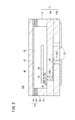
- a ceramic package according to a second configuration example (hereinafter referred to as a second package 10B) will be described with reference to FIGS.
- the second package 10B has substantially the same configuration as the first package 10A described above, but differs in the following points.
- the metal lid 40 is hermetically sealed on the frame 18 of the laminated substrate 12 using a high-temperature sealing material 42 such as silver solder.
- a bonding layer 44 is interposed between the upper surface of the frame 18 of the laminated substrate 12 and the high temperature sealing material 42.
- the bonding layer 44 includes a metallized layer 46 formed of the same material as the upper surface electrode 20 on the upper surface of the frame 18, an electrolytic plating layer 48 of, for example, nickel (Ni) formed on the metalized layer 46,
- an electroless plating layer 50 made of gold (Au) is formed on the electrolytic plating layer 48 made of Ni.
- the metal lid 40 is formed in a flat plate shape having a thickness of 0.05 to 0.20 mm, and is composed of an iron-nickel alloy plate or an iron-nickel-cobalt alloy plate.
- a brazing material such as a silver-copper eutectic brazing which is a high-temperature sealing material 42 is formed on the lower surface (the entire surface or a portion corresponding to the frame 18) of the metal lid 40.
- the thickness is about 5 to 20 ⁇ m.
- the metal lid 40 is a composite plate configured by rolling and rolling a brazing material foil such as silver-copper eutectic brazing on the lower surface of an iron-nickel alloy plate or an iron-nickel-cobalt alloy plate. It is produced by punching into a predetermined shape with a punching die.
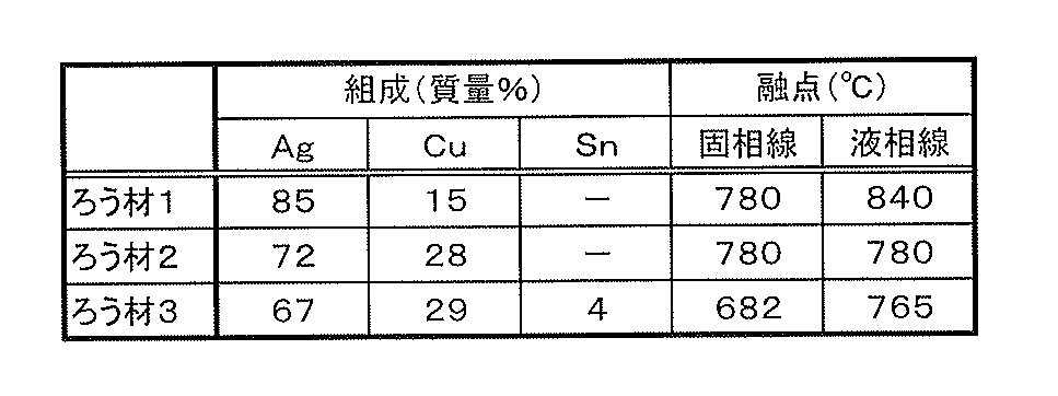
- brazing material 1 85Ag-15Cu
- brazing material 2 72Ag-28Cu
- brazing material 3 67Ag-29Cu-4Sn
- Ni electroplating layer 48 and the Au electroless plating layer 50 function as layers that improve the wettability of the high-temperature sealing material 42 to the metallized layer 46.
- step S101 of FIG. 4 a mixed powder, an organic component, and a solvent for preparing a ceramic tape are prepared.
- the mixed powder, organic component, and solvent to be prepared are the same as those in Step S1a, Step S1b, and Step S1c described above, and therefore redundant description thereof is omitted.
- step S102 the organic component and the solvent are mixed and dispersed in the above-described mixed powder.
- step S103 the ceramic substrate is formed by a known forming method such as a pressing method, a doctor blade method, a rolling method, or an injection method.
- a ceramic molded body (ceramic tape) which is a precursor of the above is prepared.
- step S104 the ceramic tape is cut and processed into a desired shape, a first tape having a large area for the first substrate 16a, a second tape having a large area for the second substrate 16b, and a frame for the frame 18.
- a third tape is manufactured, and further, a through hole for forming the first via hole 26a and the second via hole 26b is formed by micro drilling, laser processing, or the like.
- a raw material powder, an organic component and a solvent for the conductor paste are prepared.
- the raw material powder to be prepared is at least one of metal powders such as W (tungsten), Mo (molybdenum), nickel (Ni), a mixture of Cu and W, or a mixture of Cu and Mo.
- a mixed powder obtained by appropriately adding Al 2 O 3 powder, SiO 2 powder, or a powder equivalent to the ceramic base to the content of, for example, 1 to 20% by mass, particularly 8% by mass or less can be used.
- the organic component to be prepared include a resin (for example, ethyl cellulose) and a surfactant.
- the solvent to be prepared include terpineol.
- step S106 a conductive paste is prepared by mixing and dispersing the organic component and the solvent in the mixed powder.
- step S107 a conductive paste is applied by printing such as screen printing or gravure printing to the first to third tapes produced as described above.
- step S108 the first tape to the third tape on which the conductive paste is printed and applied are aligned and laminated and pressed to produce a laminated body.
- step S109 dividing grooves for dividing the chip are formed on both surfaces of the laminate by, for example, knife cutting.
- a forming gas atmosphere wetter temperature 25 to 47 ° C.
- H 2 / N 2 30% / 70%.
- a laminated original plate in which the laminate and the conductor paste are simultaneously fired is produced.
- This multi-cavity substrate has a shape in which the shapes of a large number of frames 18 are integrally arranged.
- the conductive paste becomes an electrode (the upper surface electrode 20 or the like) or the metallized layer 46 by this firing.
- the surface of the metallized layer 46 is washed with alkali, acid, or the like (pretreatment). That is, acid cleaning is performed after alkali cleaning.
- the alkali and acid may be used after diluted to an appropriate concentration.
- the pretreatment is performed at a temperature of about 20 ° C. to 70 ° C. and between several minutes to several tens of minutes.
- step S112 Ni electrolysis or electroless plating is performed to form a Ni plating layer 48 (film thickness: 1.0 to 5.0 ⁇ m) on the metallized layer 46.
- step S113 an Au electrolytic or electroless plating layer 50 (film thickness: 0.05 to 0.3 ⁇ m) is formed on the Ni plating layer 48.
- step S114 the multi-piece substrate is pressed with a pressing roller or the like and divided into a plurality of pieces (chip division), and a plurality of laminated substrates 12 each having an accommodation space 28 are produced.
- step S 115 the crystal resonator 30 is mounted on the upper surface electrode 20 via the conductor layer 32 in each accommodation space 28 of the plurality of laminated substrates 12.
- step S116 the metal lid 40 with the high temperature sealing material 42 formed on the back surface is placed on the frame 18 with the high temperature sealing material 42 and the upper surface (bonding layer 44) side of the frame 18 facing each other. Put on. Thereafter, while rolling the pair of roller electrodes of the seam welding machine in contact with the outer peripheral edges of the metal lid 40 facing each other, a current is passed between the roller electrodes, so that a part of the high-temperature sealing material 42 is removed. By melting, the metal lid body 40 is hermetically sealed on the frame body 18. The atmosphere at the time of sealing is performed in N 2 gas or vacuum. Thereby, a plurality of second packages 10B in which the crystal resonators 30 are mounted are completed.
- Example 1 Raw material powder was prepared.
- the raw material powder is 3Al 2 O 3 .2SiO 2 (mullite) powder having an average particle diameter of 1.7 ⁇ m, ZrO 2 powder having an average particle diameter of 0.5 ⁇ m, and MnO powder having an average particle diameter of 1.0 ⁇ m.
- the raw material powder was mixed at a ratio of 3Al 2 O 3 .2SiO 2 (mullite) powder: 86.3 mass%, ZrO 2 powder: 8.0 mass%, MnO powder: 5.7 mass% to obtain a mixed powder. . That is, the ceramic composition of the mixed powder, as shown in Table 2, 62.0 wt% of Al in terms of Al 2 O 3, 8.0 wt% of Zr in terms of ZrO 2, the Si in terms of SiO 2 24. 3% by mass and 5.7% by mass of Mn in terms of MnO are contained.
- Polyvinyl butyral, tertiary amine and phthalic acid ester (diisononyl phthalate: DINP) are mixed as organic components in the resulting mixed powder, and IPA (isopropyl alcohol) and toluene are mixed and diffused as solvents. After that, a ceramic tape having a thickness of 60 to 270 ⁇ m was produced by a doctor blade method.
- the obtained ceramic tape was fired in a forming gas atmosphere with a firing temperature (maximum temperature) of 1290 ° C. and H 2 + N 2 to produce a ceramic substrate according to Example 1.
- the conductor was formed by simultaneous firing.
- the ceramic substrate includes a first ceramic substrate for confirming the intensity ratio of the crystal phase and the X-ray diffraction, a second ceramic substrate for confirming the bending strength, and a third ceramic substrate for confirming the Young's modulus, A fourth ceramic substrate for measuring electrical characteristics (relative dielectric constant and dielectric loss tangent) was produced. The same applies to Examples 2 to 11 and Comparative Examples 1 and 2 described below.
- Example 2 A ceramic substrate according to Example 2 was produced in the same manner as in Example 1 described above, except that 1.4% by mass of BaO powder having an average particle diameter of 1.0 ⁇ m was added as an additive to the raw material powder. That is, the porcelain composition of Example 2 includes 1.4% by mass of Ba in terms of BaO when the total of Al 2 O 3 , ZrO 2 , SiO 2 and MnO is 100% by mass.
- Example 3 As ceramic composition of the raw material powder, 50.4 wt% of Al in terms of Al 2 O 3, 24.1 wt% of Zr in terms of ZrO 2, 19.8 wt% of Si in terms of SiO 2, the Mn in terms of MnO A ceramic substrate according to Example 3 was produced in the same manner as Example 2 described above except that 5.7% by mass was included.
- Example 4 As the porcelain composition of the raw material powder, Al is 41.8% by mass in terms of Al 2 O 3 , Zr is 36.1% by mass in terms of ZrO 2 , Si is 16.4% by mass in terms of SiO 2 , and Mn is in terms of MnO.
- a ceramic substrate according to Example 4 was produced in the same manner as Example 2 described above, except that 5.7% by mass was included.
- Example 5 A ceramic substrate according to Example 5 was produced in the same manner as Example 2 described above except for the following points.
- Al As the porcelain composition of the raw material powder, Al is 51.5% by mass in terms of Al 2 O 3 , Zr is 24.6% by mass in terms of ZrO 2 , Si is 20.2% by mass in terms of SiO 2 , and Mn is It contains 3.6% by mass in terms of MnO.
- B As an additive, Ba is contained in an amount of 0.9% by mass in terms of BaO.
- the firing temperature (maximum temperature) was set to 1320 ° C.
- Example 6 A ceramic substrate according to Example 6 was produced in the same manner as Example 2 described above, except for the following points.
- Al is 51.1% by mass in terms of Al 2 O 3
- Zr is 24.4% by mass in terms of ZrO 2
- Si is 20.1% by mass in terms of SiO 2
- Mn is Contains 4.5% by mass in terms of MnO.
- Ba is contained in an amount of 1.1% by mass in terms of BaO.
- Example 7 A ceramic substrate according to Example 7 was produced in the same manner as Example 2 described above, except for the following points.
- Al is 49.6 mass% in terms of Al 2 O 3
- Zr is 23.7 mass% in terms of ZrO 2
- Si is 19.5 mass% in terms of SiO 2
- Mn It contains 7.2% by mass in terms of MnO.
- Ba is contained in 1.8% by mass in terms of BaO.
- C The firing temperature (maximum temperature) was 1240 ° C.
- Example 8 A ceramic substrate according to Example 8 was produced in the same manner as in Example 3 described above, except that 0.5% by mass of TiO 2 powder having an average particle size of 0.3 ⁇ m was added as an additive to the raw material powder. That is, the porcelain composition of Example 8 contains 0.5% by mass of Ti in terms of TiO 2 when the total of Al 2 O 3 , ZrO 2 , SiO 2 and MnO is 100% by mass.
- Example 9 A ceramic substrate according to Example 9 was produced in the same manner as in Example 3 described above except that 0.5% by mass of CaO powder having an average particle diameter of 1.0 ⁇ m was added as an additive to the raw material powder. That is, the porcelain composition of Example 9 contains 0.5% by mass of Ca in terms of CaO when the total of Al 2 O 3 , ZrO 2 , SiO 2 and MnO is 100% by mass.
- Example 10 A ceramic substrate according to Example 10 was produced in the same manner as in Example 3 described above, except that 0.5% by mass of Y 2 O 3 powder having an average particle diameter of 1.0 ⁇ m was added as an additive to the raw material powder. did. That is, the porcelain composition of Example 10 includes 0.5% by mass of Y in terms of Y 2 O 3 when the total of Al 2 O 3 , ZrO 2 , SiO 2 and MnO is 100% by mass.
- Example 11 A ceramic substrate according to Example 11 was produced in the same manner as in Example 3 described above, except that 0.5% by mass of MgO powder having an average particle size of 0.35 ⁇ m was added as an additive to the raw material powder. That is, the porcelain composition of Example 11 includes 0.5% by mass or less of Mg in terms of MgO when the total of Al 2 O 3 , ZrO 2 , SiO 2, and MnO is 100% by mass.
- Comparative Example 1 A ceramic substrate according to Comparative Example 1 was produced in the same manner as Example 1 described above except for the following points.
- A a ceramic composition of the raw material powder, 60.9 wt% of Al in terms of Al 2 O 3, 7.2 wt% of Zr in terms of ZrO 2, 27.7 wt% of Si in terms of SiO 2, the Mn Contains 4.1% by mass in terms of MnO.
- B As an additive, Ba is contained in an amount of 1.0% by mass in terms of BaO.
- the firing temperature (maximum temperature) was 1340 ° C.
- Comparative Example 2 A ceramic substrate according to Comparative Example 2 was produced in the same manner as Example 1 described above except for the following points.
- A a ceramic composition of the raw material powder, 50.0 wt% of Al in terms of Al 2 O 3, 23.9 wt% of Zr in terms of ZrO 2, 22.7 wt% of Si in terms of SiO 2, the Mn It contains 3.4% by mass in terms of MnO.
- B As an additive, Ba is contained in an amount of 0.9% by mass in terms of BaO.
- the firing temperature (maximum temperature) was 1340 ° C.
- the first ceramic bodies of Examples 1 to 11 and Comparative Examples 1 and 2 were identified by X-ray diffraction.
- the main peak intensity of 3% or more is assumed to be the intensity of the main peak (104 plane) of alumina (92% or more of Al 2 O 3 ). That is, the contained crystal phase was confirmed based on the position of the main peak intensity (peak position) of 3% or more, the Miller index, the lattice constant, and the like with respect to the intensity of the main peak of alumina.
- Table 2 shows the breakdown of Examples 1 to 11 and Comparative Examples 1 and 2, and Table 3 shows the evaluation results.
- Table 3 shows the relative dielectric constant of the electrical characteristics was expressed as “ ⁇ r”, and the dielectric loss tangent was expressed as “tan ⁇ ”.
- Comparative Examples 1 and 2 the electrical characteristics were good and the Young's modulus was good at 240 GPa or less, but the bending strength (bending strength) was 303 MPa or less and the strength was low. This is the intensity ratio Pc / Pa 0% Al 2 O 3, crystalline phase of Al 2 O 3 is believed to be due did not precipitate.
- Comparative Example 1 had the lowest bending strength of 230 MPa. This is because the strength ratio Pb / Pa of 3Al 2 O 3 .2SiO 2 is as high as 43%, so there are many glass components, and the strength ratio of ZrO 2 is as low as 27%, so that the strength can be increased. It is thought that there was not.
- Example 1 the dielectric loss tangent was 50 ⁇ 10 ⁇ 4 or less at 1 MHz, the relative dielectric constant was 7 to 13, and the electrical characteristics were good. Moreover, the bending strength was 450 MPa to 900 MPa, the Young's modulus was 170 GPa to 240 GPa, and the mechanical properties were also good. This is presumably because the strength ratio Pc / Pa of Al 2 O 3 is 5 to 25% and the crystal phase of Al 2 O 3 is precipitated. In particular, Example 7 had the highest bending strength of 792 MPa.
- the ceramic substrate and the manufacturing method thereof according to the present invention are not limited to the above-described embodiments, and various configurations can be adopted without departing from the gist of the present invention.
Landscapes
- Engineering & Computer Science (AREA)
- Chemical & Material Sciences (AREA)
- Ceramic Engineering (AREA)
- Manufacturing & Machinery (AREA)
- Materials Engineering (AREA)
- Structural Engineering (AREA)
- Organic Chemistry (AREA)
- Compositions Of Oxide Ceramics (AREA)
Abstract
本発明は、セラミック素地及びその製造方法に関する。セラミック素地は、結晶相が、3Al2O3・2SiO2を主結晶相とし、その他、Al2O3及びZrO2を含む。曲げ強度が450Ma以上、ヤング率が240GPa以下である。
Description
本発明は、セラミック素地に関し、例えば内部に振動子等の素子が実装されるセラミック製のパッケージや高周波用回路基板等に用いて好適なセラミック素地及びその製造方法に関する。
従来のセラミック素地、例えばムライト(3Al2O3・2SiO2)を主成分とするセラミック素地(ムライト素地)として、特開2010-098049号公報、特開2012-137345号公報及び特開2012-138432号公報に記載のセラミック素地が知られている。
特開2010-098049号公報記載の多層セラミック基板は、ムライトの含有量が、前記セラミック成分の93~99質量%であり、且つ、ムライト以外の成分として、Mg及びYの少なくとも1種を含むと共に、多層セラミック基板の内部に、導電層の成分として、W及びMoの少なくとも1種を含む。
特開2012-137345号公報記載のムライト質焼結体は、主結晶相の割合を100質量%としたときに、SiをSiO2換算で1.0~3.0質量%、AlをAl2O3換算で0.4~1.0質量%、MnをMn2O3換算で1.0~4.0質量部、TiをTiO2換算で2.0~8.0質量部含有する。
特開2012-138432号公報記載のムライト質焼結体は、内部配線層の周囲の少なくとも一部に存在する第1の領域と該第1の領域以外の第2の領域とを有する。X線回折にて測定したとき、第1の領域におけるムライトのメインピーク強度に対するアルミナのメインピーク強度比が0.4以上である。第2の領域におけるムライトのメインピーク強度に対するアルミナのメインピーク強度比が0.3以下である。
一般に、セラミック素地において、曲げ強度が高くなるに従って、ヤング率も高くなる。ヤング率が高くなると、変形しにくく脆くなるため、クラックが発生しやすく、また、チップ分割時のチッピングが発生しやすくなるという問題がある。
振動子等が実装されるパッケージ用途では、セラミック成形体と金属膜を同時焼成することで、電極層や配線層が形成されたセラミック素地を得ることができる。このような場合に、セラミック素地のヤング率が高くなると、ウェアラブル機器、ICカード等に搭載される小型で低背のパッケージ用途では、曲げ応力に対してクラックが発生しやすくなる。
また、ムライト素地は、低ヤング率であるが、強度が低いため、強度の要求される例えば内部に振動子等の素子が実装されるセラミック製のパッケージには適用されていなかった。上述した特開2010-098049号公報、特開2012-137345号公報及び特開2012-138432号公報に記載の技術も、プローブカードに必要な寸法精度や耐薬品性等に重きを置いており、強度やヤング率について何ら考慮されていない。
本発明はこのような課題を考慮してなされたものであり、高周波用回路基板にも好適であり、曲げ強度が高く、しかも、ヤング率が低く、セラミック素地を用いた製品(セラミックパッケージ、高周波用回路基板等)の小型化を低コストで実現することができるセラミック素地及びその製造方法を提供することを目的とする。
[1] 第1の本発明に係るセラミック素地は、結晶相が、3Al2O3・2SiO2を主結晶相とし、その他、Al2O3及びZrO2を含むことを特徴とする。
[2] 第1の本発明において、92%以上のAl2O3を含むセラミック基板のX線回折結果における(113)面のピーク強度をPa、当該セラミック素地のX線回折結果における3Al2O3・2SiO2の(240)面のピーク強度をPbとしたとき、前記ピーク強度Paに対する前記ピーク強度Pbの比(Pb/Pa)が5~50%であることが好ましい。
[3] 第1の本発明において、92%以上のAl2O3を含むセラミック基板のX線回折結果における(113)面のピーク強度をPa、当該セラミック素地のX線回折結果におけるAl2O3の(113)面のピーク強度をPcとしたとき、前記ピーク強度Paに対する前記ピーク強度Pcの比(Pc/Pa)が5~25%であることが好ましい。
[4] 第1の本発明において、92%以上のAl2O3を含むセラミック基板のX線回折結果における(113)面のピーク強度をPa、当該セラミック素地のX線回折結果におけるt-ZrO2の(111)面のピーク強度をPt、m-ZrO2の(/111)面のピーク強度をPm1、m-ZrO2の(111)面のピーク強度をPm2としたとき、前記ピーク強度Paに対する前記ピーク強度Pt、Pm1及びPm2の合計の比{(Pt+Pm1+Pm2)/Pa)}が15~200%であることが好ましい。

[5] 第1の本発明において、AlをAl2O3換算で40.0~70.0質量%、ZrをZrO2換算で5.0~40.0質量%、SiをSiO2換算で10.0~30.0質量%、MnをMnO換算で2.0~8.0質量%を含むことが好ましい。
[6] この場合、Ba、Ti、Y、Ca及びMgのうち、少なくとも1種の元素を含み、Al2O3、ZrO2、SiO2及びMnOの合計を100質量%としたとき、Baを含む場合は、BaO換算で1.5質量%以下含み、Tiを含む場合は、TiO2換算で1.5質量%以下含み、Yを含む場合は、Y2O3換算で1.5質量%以下含み、Caを含む場合は、CaO換算で1.5質量%以下含み、Mgを含む場合は、MgO換算で1.5質量%以下含んでもよい。
[7] 第1の本発明において、温度1200~1400℃にて焼結されていることが好ましい。
[8] 第1の本発明において、曲げ強度が450Ma以上、ヤング率が240GPa以下である。
[9] この場合、曲げ強度が450MPa以上900MPa以下、ヤング率が170GPa以上240GPa以下であることが好ましい。
[10] 第1の本発明において、誘電正接が、1MHzにおいて、50×10-4以下であり、比誘電率が7~13であることが好ましい。
[11] 第2の本発明に係るセラミック素地の製造方法は、AlをAl2O3換算で40.0~70.0質量%、ZrをZrO2換算で5.0~40.0質量%、SiをSiO2換算で10.0~30.0質量%、MnをMnO換算で2.0~8.0質量%を含有する成形体を作製する成形体作製工程と、前記成形体を1200~1400℃にて焼成する焼成工程とを備えることを特徴とする。
[12] 第2の本発明において、前記成形体は、Ba、Ti、Y、Ca及びMgのうち、少なくとも1種の元素を含み、Al2O3、ZrO2、SiO2及びMnOの合計を100質量%としたとき、Baを含む場合は、BaO換算で1.5質量%以下含み、Tiを含む場合は、TiO2換算で1.5質量%以下含み、Yを含む場合は、Y2O3換算で1.5質量%以下含み、Caを含む場合は、CaO換算で1.5質量%以下含み、Mgを含む場合は、MgO換算で1.5質量%以下含んでもよい。
[13] 第2の本発明において、前記成形体作製工程の後に、前記成形体に、金属を含む導体層を形成する工程をさらに備え、前記焼成工程では、前記導体層が形成された成形体を焼成してもよい。
[14] 第2の本発明において、前記焼成工程は、水素を5%以上含む、水素と窒素のフォーミングガス中で行ってもよい。
本発明に係るセラミック素地及びその製造方法によれば、以下の効果を奏する。
(a) 曲げ強度が高く、しかも、ヤング率が低い。
(b) 高周波用回路基板にも好適である。
(c) チップ分割時のチッピング発生率も小さい。
(d) パッケージ部品等として搭載された際の曲げ応力による破壊がし難い。
(e) ロウ付けする際のクラックが発生し難い。
(f) 歩留りを向上させることができ、セラミック素地を用いた製品(セラミックパッケージ、高周波用回路基板等)の小型化を低コストで実現することができる。
(g) 低温焼成のため、電極や配線として例えばCu(銅)-W(タングステン)等の低抵抗導体を用いることができる。
(a) 曲げ強度が高く、しかも、ヤング率が低い。
(b) 高周波用回路基板にも好適である。
(c) チップ分割時のチッピング発生率も小さい。
(d) パッケージ部品等として搭載された際の曲げ応力による破壊がし難い。
(e) ロウ付けする際のクラックが発生し難い。
(f) 歩留りを向上させることができ、セラミック素地を用いた製品(セラミックパッケージ、高周波用回路基板等)の小型化を低コストで実現することができる。
(g) 低温焼成のため、電極や配線として例えばCu(銅)-W(タングステン)等の低抵抗導体を用いることができる。
以下、本発明に係るセラミック素地及びその製造方法の実施の形態例を図1~図4を参照しながら説明する。なお、本明細書において数値範囲を示す「~」は、その前後に記載される数値を下限値及び上限値として含む意味として使用される。
本実施の形態に係るセラミック素地は、結晶相が、3Al2O3・2SiO2を主結晶相とし、その他、Al2O3及びZrO2を含む。
X線回折結果で見た場合、3Al2O3・2SiO2に関しては、92%以上のAl2O3を含むセラミック基板のX線回折結果における(113)面のピーク強度をPa、セラミック素地のX線回折結果における3Al2O3・2SiO2の(240)面のピーク強度をPbとしたとき、ピーク強度Paに対するピーク強度Pbの比(Pb/Pa)が5~50%であることが好ましい。
Al2O3に関しては、セラミック素地のX線回折結果におけるAl2O3の(113)面のピーク強度をPcとしたとき、ピーク強度Paに対するピーク強度Pcの比(Pc/Pa)が5~25%であることが好ましい。
ZrO2に関しては、セラミック素地のX線回折結果におけるt-ZrO2の(111)面のピーク強度をPt、m-ZrO2の(/111)面のピーク強度をPm1、m-ZrO2の(111)面のピーク強度をPm2としたとき、ピーク強度Paに対する前記ピーク強度Pt、Pm1及びPm2の合計の比{(Pt+Pm1+Pm2)/Pa)}が15~200%であることが好ましい。
磁器組成としては、AlをAl2O3換算で40.0~70.0質量%、ZrをZrO2換算で5.0~40.0質量%、SiをSiO2換算で10.0~30.0質量%、MnをMnO換算で2.0~8.0質量%を含むことが好ましい。
添加剤として、Ba、Ti、Y、Ca及びMgのうち、少なくとも1種の元素を含んでもよい。Al2O3、ZrO2、SiO2及びMnOの合計を100質量%としたとき、Baを含む場合は、BaO換算で1.5質量%以下含み、Tiを含む場合は、TiO2換算で1.5質量%以下含み、Yを含む場合は、Y2O3換算で1.5質量%以下含み、Caを含む場合は、CaO換算で1.5質量%以下含み、Mgを含む場合は、MgO換算で1.5質量%以下含むことが好ましい。
これにより、機械特性として、曲げ強度の向上をもたらしながらも、低ヤング率を達成できる。具体的には、曲げ強度が450Ma以上、ヤング率が240GPa以下を実現することができる。より詳細には、曲げ強度が450MPa以上900MPa以下、ヤング率が170GPa以上240GPa以下を実現することができる。なお、「曲げ強度」とは、4点曲げ強度をいい、JISR1601(ファインセラミックスの曲げ試験方法)に基づいて室温にて測定した値をいう。
また、電気特性として、誘電正接が、1MHzにおいて、50×10-4以下、比誘電率が7~13を実現することができる。
このセラミック素地は、例えば3Al2O3・2SiO2(ムライト)粉末を50~93質量%、ZrO2粉末を5~40質量%、Al2O3粉末を0~36質量%、SiO2粉末を0~16質量%、MnO粉末を2~8質量%含有する成形体を作製した後、成形体を1200~1400℃にて焼成することにより作製される。
この場合、3Al2O3・2SiO2粉末の平均粒度が0.5~4.0μm、ZrO2粉末の平均粒度が0.05~1.0μm、Al2O3粉末の平均粒度が0.3~2.5μm、SiO2粉末の平均粒度が0.1~2.5μm、MnO粉末の平均粒度が0.5~4.0μmであることが好ましい。
もちろん、成形体には添加剤を含有させてもよい。添加剤としては、BaO粉末、TiO2粉末、Y2O3粉末、CaO粉末、MgO粉末のうち、少なくとも1種の粉末が挙げられる。
添加剤の量としては、Al2O3粉末、ZrO2粉末、SiO2粉末及びMnO粉末の合計を100質量%としたとき、少なくとも1種の粉末を1.5質量%以下含むことが好ましい。
この場合、BaO粉末の平均粒度が0.5~4.0μm、TiO2粉末の平均粒度が0.05~1.0μm、Y2O3粉末の平均粒度が0.1~5.0μm、CaO粉末の平均粒度が0.5~2.0μm、MgO粉末の平均粒度が0.1~1.0μmであることが好ましい。
原料の平均粒度は、レーザー回折散乱式粒度分布測定法(HORIBA製、LA-920)により測定して得られる体積基準粒度分布において、小粒径側からの通過分積算(積算通過分率)50%の粒子径をいう。
Mnを含むことによって、低温焼成を可能にし、粒成長を抑制することができ、強度を向上させることができる。ZrO2を含むことによって、さらに高強度化が可能となる。すなわち、一般に、ヤング率が低いムライト(3Al2O3・2SiO2)を主成分とするセラミック素地の強度を向上させることができる。
また、添加剤によって、ムライトのシリカ成分を抜き取り、これにより、アルミナ(Al2O3)を析出させて強度を高めることができる。添加剤の量を調整し、アルミナを析出させる量を増減することで、ヤング率と強度を制御することができる。
なお、必要に応じて、着色剤としてMo(モリブデン)酸化物やW(タングステン)酸化物やCr(クロム)酸化物を1.0質量%以下含めるようにしてもよい。
このように、本実施の形態に係るセラミック素地は、温度1200~1400℃という低温にて焼結することができ、曲げ強度が450MPa以上、ヤング率が240GPa以下のセラミック素地を実現することができる。具体的には、曲げ強度が450MPa以上900MPa以下、ヤング率が170GPa以上240GPa以下のセラミック素地を実現することができる。
一般に、セラミック素地において、曲げ強度が高くなるに従って、ヤング率も高くなる。ヤング率が高くなると、変形しにくく脆くなるため、クラックが発生しやすく、また、チップ分割時のチッピングが発生しやすくなるという問題がある。
しかし、本実施の形態に係るセラミック素地は、高周波用回路基板にも好適であり、曲げ強度が450MPa以上であっても、ヤング率が240GPa以下と低いことから、チップ分割時のチッピング発生率も小さく、パッケージ部品等として搭載された際の曲げ応力による破壊がし難く、ロウ付けする際のクラックが発生し難く歩留りを向上させることができ、セラミック素地を用いた製品(セラミックパッケージ、高周波用回路基板等)の小型化を低コストで実現することができる。
Alの含有量をAl2O3換算で40.0~70.0質量%とすることで、生成されるAl2O3の量が最適となり、焼成温度が上昇しても、Al2O3の結晶粒径の増大を抑えることができ、もって曲げ強度の向上を図り易くなる。
Zrの含有量をZrO2換算で5.0~40.0質量%とすることで、曲げ強度が向上し易くなると共に、ヤング率が高くなるのを抑えることができ、また、誘電率の増大や熱伝導率の低下を抑えることができる。
Siの含有量をSiO2換算で10.0~30.0質量%とすることで、生成されるガラス相の量の低下を抑えることができ、1200~1400℃での緻密化を達成し易くなり、また、生成されるガラスの軟化温度の低下並びに気孔率の増大を抑えることができる。さらに、曲げ強度の低下を抑えることができる。
Mnの含有量をMnO換算で2.0~8.0質量%とすることで、生成されるガラス相の量の低下を抑えることができ、1200~1400℃での緻密化を達成し易くなり、また、生成されるガラスの軟化温度の低下並びに気孔率の増大を抑えることができる。さらに、曲げ強度の低下を抑えることができる。
従って、Al、Zr、Si、Mnを上述した比率で含有させることで、磁器の焼成温度を適正化でき、生成されるガラス相の強度を高めることができ、ヤング率が低いムライトを含むセラミック素地の曲げ強度を向上させることができる。しかも、低い焼成温度にて作製することができ、コストの低廉化に有利になる。さらに、例えば押圧ローラーによるチップ分割でのチッピング発生率を低下させることができ、生産性を向上させることができる。電気特性(誘電正接)も低く抑えることができ、例えば高周波用回路基板に用いて好ましい。しかも、低温焼成で作製することができるため、電極や配線として例えばCu(銅)-W(タングステン)等の低抵抗導体を用いることができる。ここで、低抵抗とは、厚みが15μmの表面抵抗が10mΩ/sq.以下をいう。
ここで、本実施の形態に係るセラミック素地を用いたセラミックパッケージの2つの構成例について図1~図4を参照しながら説明する。
第1の構成例に係るセラミックパッケージ(以下、第1パッケージ10Aと記す)は、図1に示すように、本実施の形態に係るセラミック素地にて構成された積層基板12と、同じく本実施の形態に係るセラミック素地にて構成された蓋体14とを有する。
積層基板12は、少なくとも板状の第1基板16aと、板状の第2基板16bと、枠体18とがこの順番で積層されて構成されている。また、この積層基板12は、第2基板16bの上面に形成された上面電極20と、第1基板16aの下面に形成された下面電極22と、内部に形成された内層電極24と、該内層電極24と下面電極22とを電気的に接続する第1ビアホール26aと、内層電極24と上面電極20とを電気的に接続する第2ビアホール26bとを有する。
また、この第1パッケージ10Aは、第2基板16bの上面と枠体18とで囲まれた収容空間28に、水晶振動子30が導体層32を介して上面電極20に電気的に接続されている。さらに、水晶振動子30を保護するため、枠体18の上面に、蓋体14がガラス層34を介して気密に封止されている。
上述した第1パッケージ10Aでは、収容空間28内に、水晶振動子30を実装した例を示したが、その他、抵抗体、フィルタ、コンデンサ、半導体素子のうち、少なくとも1種以上を実装してもよい。本実施の形態では、誘電正接が1MHzにおいて、50×10-4以下、比誘電率が7~13であるため、高周波用回路基板としても好適である。
そして、第1パッケージ10Aを構成する積層基板12及び蓋体14は、本実施の形態に係るセラミック素地にて構成しているため、曲げ強度が450MPa以上で、ヤング率が240GPa以下である。なお、「曲げ強度」とは、4点曲げ強度をいい、JISR1601(ファインセラミックスの曲げ試験方法)に基づいて室温にて測定した値をいう。
そして、本実施の形態に係るセラミック素地が、上述した組成を有することから、温度1200~1400℃という低温にて焼結させることができる。そのため、セラミック素地の前駆体(焼成前の成形体)と、電極(上面電極20、下面電極22、内層電極24)及びビアホール26(第1ビアホール26a、第2ビアホール26b)とを同時焼成することで、積層基板12を作製することができ、製造工程を簡略化することができる。
次に、セラミック素地の製造方法を、例えば第1パッケージ10Aの製造方法に沿って図2を参照しながら説明する。
先ず、図2のステップS1aにおいて、3Al2O3・2SiO2(ムライト)粉末を50~93質量%、ZrO2粉末を5~40質量%、Al2O3粉末を0~36質量%、SiO2粉末を0~16質量%、MnO粉末を2~8質量%含有する混合粉末を準備し、ステップS1bにおいて、有機成分(バインダー)を準備し、ステップS1cにおいて、溶剤を準備する。
3Al2O3・2SiO2粉末の平均粒度は0.5~4.0μmが好ましい。ZrO2粉末の平均粒度は0.05~1.0μmが好ましい。Al2O3粉末の平均粒度は0.3~2.5μmが好ましい。この範囲であれば、均一な磁器を得る上で好適であり、緻密化による強度の向上、Al2O3及びZrO2自身の焼結性の向上を図ることができる。
SiO2粉末の平均粒度は0.1~2.5μmが好ましい。MnO粉末の平均粒度は0.5~4.0μmが好ましい。これらSiO2粉末、MnO粉末において、好ましい範囲であれば、粒子の分散性の向上、組成の均一化をもたらし、強度の向上を図ることができる。
ステップS1bにおいて準備される有機成分(バインダー)は、樹脂、界面活性剤、可塑剤等が挙げられる。樹脂としては、例えばポリビニルブチラールが挙げられ、界面活性剤としては、例えば3級アミンが挙げられ、可塑剤としては、例えばフタル酸エステル(例えばフタル酸ジイソノニル:DINP)が挙げられる。
ステップS1cにおいて準備される溶剤は、アルコール系溶剤、芳香族系溶剤等が挙げられる。アルコール系溶剤としては、例えばIPA(イソプロピルアルコール)が挙げられ、芳香族系溶剤としては、例えばトルエンが挙げられる。
そして、次のステップS2において、上述の混合粉末に、有機成分及び溶剤を混合、分散させた後、ステップS3において、プレス法、ドクターブレード法、圧延法、射出法等の周知の成形方法によって、セラミック素地の前駆体であるセラミック成形体(セラミックテープとも記す)を作製する。例えば混合粉末に有機成分や溶剤を添加してスラリーを調製した後、ドクターブレード法によって所定の厚みのセラミックテープを作製する。あるいは、混合粉末に有機成分を加え、プレス成形、圧延成形等により所定の厚みのセラミックテープを作製する。
ステップS4において、セラミックテープを所望の形状に切断、加工して、第1基板16a用の広い面積の第1テープと、第2基板16b用の広い面積の第2テープと、枠体18用の第3テープと、蓋体14用の第4テープを作製し、さらに金型による打ち抜き加工、マイクロドリル加工、レーザー加工等により、第1ビアホール26a及び第2ビアホール26bを形成するための貫通孔を形成する。
次に、ステップS5において、上述のように作製した第1テープ及び第2テープに対して、上面電極20、下面電極22、内層電極24を形成するための導体ペーストをスクリーン印刷、グラビア印刷等の方法により印刷塗布し、さらに、所望により、導体ペーストを貫通孔内に充填する。
導体ペーストは、導体成分として、例えばW(タングステン)、Mo(モリブデン)等の高融点金属のうち少なくとも1種、あるいはCuとWとの混合物、あるいはCuとMoとの混合物を用い、これにAl2O3粉末、又はSiO2粉末、又はセラミック素地と同等の粉末を例えば1~20質量%、特に8質量%以下の割合で添加したものが好ましい。これにより、導体層の導通抵抗を低く維持したままアルミナ焼結体と導体層の密着性を高め、めっき欠け等の不良の発生を防止することができる。
その後、ステップS6において、導体ペーストを印刷塗布した第1テープ及び第2テープ並びに枠体用の第3テープを位置合わせし、積層圧着して、積層体を作製する。
その後、ステップS7において、積層体の両面にチップ分割のための分割溝を例えばナイフカットにて形成する。
次のステップS8において、積層体及び第4テープを、水素を5%以上含む、水素と窒素のフォーミングガス雰囲気、例えばH2/N2=30%/70%のフォーミングガス雰囲気(ウェッター温度25~47℃)で、1200~1400℃の温度範囲で焼成する。これによって、積層体及び導体ペーストが同時焼成された積層原板(多数個取り基板)が作製される。この焼成によって、上述したように、結晶相が、3Al2O3・2SiO2を主結晶相とし、その他、Al2O3及びZrO2を含むセラミック素地、すなわち、多数個取り基板を作製することができる。また、導体ペーストとして、CuとWとの混合物あるいはCuとMoとの混合物を用いた場合は、Cu-WあるいはCu-Moの低抵抗導体とすることができる。
焼成雰囲気を、上述のようなフォーミングガス雰囲気で行うことで、導体ペースト中の金属の酸化を防止することができる。焼成温度は、上述した温度範囲が好ましい。緻密化を促進させることができ、曲げ強度を向上させることができる。また、積層体を構成する第1テープ、第2テープ及び第3テープの収縮率のばらつきを少なくすることができ、寸法精度の向上、並びに歩留まりの向上も図ることができる。焼成温度を高くする必要がないため、それだけ設備にコストをかける必要がない。
次に、ステップS9において、上述の多数個取り基板にめっき処理を行って、該多数個取り基板の表面に形成されている導体層に、Ni、Co、Cr、Au、Pd及びCuのうち、少なくとも1種からなるめっき層を形成し、多数個取り基板の表面に多数の上面電極20及び多数の下面電極22を形成する。
その後、ステップS10において、多数個取り基板を、押圧ローラー等で押し当てて複数に分割し(チップ分割)、収容空間28を有する複数の積層基板12を作製する。ステップS11において、複数の積層基板12の各収容空間28にそれぞれ水晶振動子30を上面電極20に導体層32を介して実装する。
そして、ステップS12において、各積層基板12の上面に、封止用のガラス層34が形成されたセラミック製の蓋体14により気密に封止(蓋接合)することによって、内部に水晶振動子30が実装された複数の第1パッケージ10Aが完成する。
この第1パッケージ10Aの製造方法(セラミック素地の製造方法)においては、上述したように、結晶相が、3Al2O3・2SiO2を主結晶相とし、その他、Al2O3及びZrO2を含む、高周波用回路基板にも好適であり、曲げ強度が450MPa以上、ヤング率が240GPa以下のセラミック素地を作製することができる。また、チップ分割時のチッピング発生率も小さく、歩留りを向上させることができ、セラミック素地を用いた製品(セラミックパッケージ、高周波用回路基板等)の小型化を低コストで実現することができるセラミック素地を、低い焼成温度にて作製することができる。
次に、第2の構成例に係るセラミックパッケージ(以下、第2パッケージ10Bと記す)について、図3及び図4を参照しながら説明する。
この第2パッケージ10Bは、図3に示すように、上述した第1パッケージ10Aとほぼ同様の構成を有するが、以下の点で異なる。
すなわち、金属蓋体40を、積層基板12の枠体18上に、銀ろう等の高温封止材42を用いて気密封止している。
また、積層基板12の枠体18の上面と高温封止材42との間に接合層44が介在されている。この接合層44は、枠体18の上面に、上面電極20と同じ材料で形成されたメタライズ層46と、該メタライズ層46上に形成された例えばニッケル(Ni)の電解めっき層48と、該Niの電解めっき層48上に形成された例えば金(Au)の無電解めっき層50とを有する。
金属蓋体40は、厚みが0.05~0.20mmの平板状に形成され、鉄-ニッケル合金板あるいは鉄-ニッケル-コバルト合金板にて構成されている。この金属蓋体40の下面(全面あるいは枠体18に対応した部分)には、高温封止材42である銀-銅共晶ろう等のろう材が形成されている。厚みは5~20μm程度である。
具体的には、金属蓋体40は、鉄-ニッケル合金板あるいは鉄-ニッケル-コバルト合金板の下面に銀-銅共晶ろう等のろう材箔を重ねて圧延して構成される複合板を打ち抜き金型で所定の形状に打ち抜くことによって作製される。
高温封止材42としては、下記表1に示すろう材1(85Ag-15Cu)、ろう材2(72Ag-28Cu)、ろう材3(67Ag-29Cu-4Sn)等を使用することができる。
Niの電解めっき層48及びAuの無電解めっき層50は、高温封止材42のメタライズ層46に対する濡れ性を向上させる層として機能する。
次に、第2パッケージ10Bの製造方法を図4を参照しながら説明する。なお、図2と重複する工程については説明を省略する。
先ず、図4のステップS101において、セラミックテープを作製するための混合粉末、有機成分及び溶剤を準備する。準備する混合粉末、有機成分及び溶剤は、上述したステップS1a、ステップS1b及びステップS1cと同じであるため、その重複説明を省略する。
そして、ステップS102において、上述の混合粉末に、有機成分及び溶剤を混合、分散させた後、ステップS103において、プレス法、ドクターブレード法、圧延法、射出法等の周知の成形方法によって、セラミック素地の前駆体であるセラミック成形体(セラミックテープ)を作製する。
ステップS104において、セラミックテープを所望の形状に切断、加工して、第1基板16a用の広い面積の第1テープと、第2基板16b用の広い面積の第2テープと、枠体18用の第3テープとを作製し、さらに、マイクロドリル加工、レーザー加工等により、第1ビアホール26a及び第2ビアホール26bを形成するための貫通孔を形成する。
一方、ステップS105において、導体ペースト用の原料粉末、有機成分及び溶剤を準備する。準備する原料粉末は、上述したように、W(タングステン)、Mo(モリブデン)、ニッケル(Ni)等の金属粉末のうち少なくとも1種、あるいはCuとWとの混合物、あるいはCuとMoとの混合物と、これに適宜Al2O3粉末、又はSiO2粉末、又はセラミック素地と同等の粉末を例えば1~20質量%、特に8質量%以下の割合で添加した混合粉末が挙げられる。準備する有機成分は、樹脂(例えばエチルセルロース)、界面活性剤等が挙げられる。準備する溶剤は、ターピネオール(terpineol)等が挙げられる。
そして、ステップS106において、上述の混合粉末に、有機成分及び溶剤を混合、分散させて導体ペーストを調製する。
次に、ステップS107において、上述のように作製した第1テープ~第3テープに対して、導体ペーストをスクリーン印刷、グラビア印刷等の方法により印刷塗布する。
その後、ステップS108において、導体ペーストを印刷塗布した第1テープ~第3テープを位置合わせし、積層圧着して、積層体を作製する。
その後、ステップS109において、積層体の両面にチップ分割のための分割溝を例えばナイフカットにて形成する。
次のステップS110において、積層体を、H2/N2=30%/70%のフォーミングガス雰囲気(ウェッター温度25~47℃)で、1200~1400℃の温度範囲で焼成する。これによって、積層体及び導体ペーストが同時焼成された積層原板(多数個取り基板)が作製される。この多数個取り基板は、多数の枠体18の形状が一体に配列された形状を有する。また、この焼成によって、導体ペーストが電極(上面電極20等)やメタライズ層46となる。
次のステップS111において、アルカリ、酸等で少なくともメタライズ層46の表面を洗浄する(前処理)。すなわち、アルカリ洗浄を行った後、酸洗浄を行う。前処理では、アルカリ及び酸は適当な濃度に希釈されて使用されてもよい。また、前処理は、20℃から70℃程度の温度と、数分から数十分の間で実施される。
ステップS112において、Niの電解あるいは無電解めっき処理を行って、メタライズ層46上にNiのめっき層48(膜厚:1.0~5.0μm)を形成する。
ステップS113において、Niのめっき層48上にAuの電解あるいは無電解めっき層50(膜厚:0.05~0.3μm)を形成する。
その後、ステップS114において、多数個取り基板を、押圧ローラー等で押し当てて複数に分割し(チップ分割)、それぞれ収容空間28を有する複数の積層基板12を作製する。その後、ステップS115において、複数の積層基板12の各収容空間28にそれぞれ水晶振動子30を上面電極20に導体層32を介して実装する。
そして、ステップS116において、裏面に高温封止材42が形成された金属蓋体40を、高温封止材42と枠体18の上面(接合層44)側とを対向させて、枠体18上に被せる。その後、金属蓋体40の相対向する外周縁にシーム溶接機の一対のローラー電極を接触させながら転動させると共に、このローラー電極間に電流を流すことで、高温封止材42の一部を溶融させることにより、枠体18上に金属蓋体40を気密封止する。封止時の雰囲気は、N2ガス又は真空中で行われる。これにより、内部に水晶振動子30が実装された複数の第2パッケージ10Bが完成する。
実施例1~11、比較例1及び2について、セラミック素地の結晶相、各結晶相におけるX線回折の強度比、機械特性(曲げ強度(抗折強度)及びヤング率)、電気特性(比誘電率及び誘電正接)を確認した。
(実施例1)
原料粉末を準備した。原料粉末は、平均粒径1.7μmの3Al2O3・2SiO2(ムライト)粉末、平均粒径0.5μmのZrO2粉末、平均粒径1.0μmのMnO粉末である。
原料粉末を準備した。原料粉末は、平均粒径1.7μmの3Al2O3・2SiO2(ムライト)粉末、平均粒径0.5μmのZrO2粉末、平均粒径1.0μmのMnO粉末である。
原料粉末を3Al2O3・2SiO2(ムライト)粉末:86.3質量%、ZrO2粉末:8.0質量%、MnO粉末:5.7質量%の割合で混合して混合粉末を得た。すなわち、混合粉末の磁器組成は、表2に示すように、AlをAl2O3換算で62.0質量%、ZrをZrO2換算で8.0質量%、SiをSiO2換算で24.3質量%、MnをMnO換算で5.7質量%含む。
得られた混合粉末に、有機成分として、ポリビニルブチラール、3級アミン及びフタル酸エステル(フタル酸ジイソノニル:DINP)を混合し、溶剤として、IPA(イソプロピルアルコール)及びトルエンを混合、拡散してスラリーを調製し、その後、ドクターブレード法にて厚さ60~270μmのセラミックテープを作製した。
得られたセラミックテープを焼成温度(最高温度)が1290℃、H2+N2のフォーミングガス雰囲気にて焼成して実施例1に係るセラミック素地を作製した。導体は同時焼成にて形成した。セラミック素地は、結晶相及びX線回折の強度比を確認するための第1セラミック素地と、曲げ強度を確認するための第2セラミック素地と、ヤング率を確認するための第3セラミック素地と、電気特性(比誘電率及び誘電正接)を測定するための第4セラミック素地を作製した。以下に説明する実施例2~11並びに比較例1及び2についても同様である。
(実施例2)
原料粉末に対し、添加剤として平均粒径1.0μmのBaO粉末を1.4質量%添加した点以外は、上述した実施例1と同様にして実施例2に係るセラミック素地を作製した。すなわち、実施例2の磁器組成は、Al2O3、ZrO2、SiO2及びMnOの合計を100質量%としたとき、BaをBaO換算で1.4質量%含む。
原料粉末に対し、添加剤として平均粒径1.0μmのBaO粉末を1.4質量%添加した点以外は、上述した実施例1と同様にして実施例2に係るセラミック素地を作製した。すなわち、実施例2の磁器組成は、Al2O3、ZrO2、SiO2及びMnOの合計を100質量%としたとき、BaをBaO換算で1.4質量%含む。
(実施例3)
原料粉末の磁器組成として、AlをAl2O3換算で50.4質量%、ZrをZrO2換算で24.1質量%、SiをSiO2換算で19.8質量%、MnをMnO換算で5.7質量%含む点以外は、上述した実施例2と同様にして実施例3に係るセラミック素地を作製した。
原料粉末の磁器組成として、AlをAl2O3換算で50.4質量%、ZrをZrO2換算で24.1質量%、SiをSiO2換算で19.8質量%、MnをMnO換算で5.7質量%含む点以外は、上述した実施例2と同様にして実施例3に係るセラミック素地を作製した。
(実施例4)
原料粉末の磁器組成として、AlをAl2O3換算で41.8質量%、ZrをZrO2換算で36.1質量%、SiをSiO2換算で16.4質量%、MnをMnO換算で5.7質量%を含む点以外は、上述した実施例2と同様にして実施例4に係るセラミック素地を作製した。
原料粉末の磁器組成として、AlをAl2O3換算で41.8質量%、ZrをZrO2換算で36.1質量%、SiをSiO2換算で16.4質量%、MnをMnO換算で5.7質量%を含む点以外は、上述した実施例2と同様にして実施例4に係るセラミック素地を作製した。
(実施例5)
以下の点以外は、上述した実施例2と同様にして実施例5に係るセラミック素地を作製した。
(a) 原料粉末の磁器組成として、AlをAl2O3換算で51.5質量%、ZrをZrO2換算で24.6質量%、SiをSiO2換算で20.2質量%、MnをMnO換算で3.6質量%を含む。
(b) 添加剤として、BaをBaO換算で0.9質量%含む。
(c) 焼成温度(最高温度)を1320℃とした。
以下の点以外は、上述した実施例2と同様にして実施例5に係るセラミック素地を作製した。
(a) 原料粉末の磁器組成として、AlをAl2O3換算で51.5質量%、ZrをZrO2換算で24.6質量%、SiをSiO2換算で20.2質量%、MnをMnO換算で3.6質量%を含む。
(b) 添加剤として、BaをBaO換算で0.9質量%含む。
(c) 焼成温度(最高温度)を1320℃とした。
(実施例6)
以下の点以外は、上述した実施例2と同様にして実施例6に係るセラミック素地を作製した。
(a) 原料粉末の磁器組成として、AlをAl2O3換算で51.1質量%、ZrをZrO2換算で24.4質量%、SiをSiO2換算で20.1質量%、MnをMnO換算で4.5質量%含む。
(b) 添加剤として、BaをBaO換算で1.1質量%含む。
以下の点以外は、上述した実施例2と同様にして実施例6に係るセラミック素地を作製した。
(a) 原料粉末の磁器組成として、AlをAl2O3換算で51.1質量%、ZrをZrO2換算で24.4質量%、SiをSiO2換算で20.1質量%、MnをMnO換算で4.5質量%含む。
(b) 添加剤として、BaをBaO換算で1.1質量%含む。
(実施例7)
以下の点以外は、上述した実施例2と同様にして実施例7に係るセラミック素地を作製した。
(a) 原料粉末の磁器組成として、AlをAl2O3換算で49.6質量%、ZrをZrO2換算で23.7質量%、SiをSiO2換算で19.5質量%、MnをMnO換算で7.2質量%を含む。
(b) 添加剤として、BaをBaO換算で1.8質量%含む。
(c) 焼成温度(最高温度)を1240℃とした。
以下の点以外は、上述した実施例2と同様にして実施例7に係るセラミック素地を作製した。
(a) 原料粉末の磁器組成として、AlをAl2O3換算で49.6質量%、ZrをZrO2換算で23.7質量%、SiをSiO2換算で19.5質量%、MnをMnO換算で7.2質量%を含む。
(b) 添加剤として、BaをBaO換算で1.8質量%含む。
(c) 焼成温度(最高温度)を1240℃とした。
(実施例8)
原料粉末に対し、添加剤として平均粒径0.3μmのTiO2粉末を0.5質量%添加した点以外は、上述した実施例3と同様にして実施例8に係るセラミック素地を作製した。すなわち、実施例8の磁器組成は、Al2O3、ZrO2、SiO2及びMnOの合計を100質量%としたとき、TiをTiO2換算で0.5質量%含む。
原料粉末に対し、添加剤として平均粒径0.3μmのTiO2粉末を0.5質量%添加した点以外は、上述した実施例3と同様にして実施例8に係るセラミック素地を作製した。すなわち、実施例8の磁器組成は、Al2O3、ZrO2、SiO2及びMnOの合計を100質量%としたとき、TiをTiO2換算で0.5質量%含む。
(実施例9)
原料粉末に対し、添加剤として平均粒径1.0μmのCaO粉末を0.5質量%添加した点以外は、上述した実施例3と同様にして実施例9に係るセラミック素地を作製した。すなわち、実施例9の磁器組成は、Al2O3、ZrO2、SiO2及びMnOの合計を100質量%としたとき、CaをCaO換算で0.5質量%含む。
原料粉末に対し、添加剤として平均粒径1.0μmのCaO粉末を0.5質量%添加した点以外は、上述した実施例3と同様にして実施例9に係るセラミック素地を作製した。すなわち、実施例9の磁器組成は、Al2O3、ZrO2、SiO2及びMnOの合計を100質量%としたとき、CaをCaO換算で0.5質量%含む。
(実施例10)
原料粉末に対し、添加剤として平均粒径1.0μmのY2O3粉末を0.5質量%添加した点以外は、上述した実施例3と同様にして実施例10に係るセラミック素地を作製した。すなわち、実施例10の磁器組成は、Al2O3、ZrO2、SiO2及びMnOの合計を100質量%としたとき、YをY2O3換算で0.5質量%含む。
原料粉末に対し、添加剤として平均粒径1.0μmのY2O3粉末を0.5質量%添加した点以外は、上述した実施例3と同様にして実施例10に係るセラミック素地を作製した。すなわち、実施例10の磁器組成は、Al2O3、ZrO2、SiO2及びMnOの合計を100質量%としたとき、YをY2O3換算で0.5質量%含む。
(実施例11)
原料粉末に対し、添加剤として平均粒径0.35μmのMgO粉末を0.5質量%添加した点以外は、上述した実施例3と同様にして実施例11に係るセラミック素地を作製した。すなわち、実施例11の磁器組成は、Al2O3、ZrO2、SiO2及びMnOの合計を100質量%としたとき、MgをMgO換算で0.5質量%以下含む。
原料粉末に対し、添加剤として平均粒径0.35μmのMgO粉末を0.5質量%添加した点以外は、上述した実施例3と同様にして実施例11に係るセラミック素地を作製した。すなわち、実施例11の磁器組成は、Al2O3、ZrO2、SiO2及びMnOの合計を100質量%としたとき、MgをMgO換算で0.5質量%以下含む。
(比較例1)
以下の点以外は、上述した実施例1と同様にして比較例1に係るセラミック素地を作製した。
(a) 原料粉末の磁器組成として、AlをAl2O3換算で60.9質量%、ZrをZrO2換算で7.2質量%、SiをSiO2換算で27.7質量%、MnをMnO換算で4.1質量%含む。
(b) 添加剤として、BaをBaO換算で1.0質量%含む。
(c) 焼成温度(最高温度)を1340℃とした。
以下の点以外は、上述した実施例1と同様にして比較例1に係るセラミック素地を作製した。
(a) 原料粉末の磁器組成として、AlをAl2O3換算で60.9質量%、ZrをZrO2換算で7.2質量%、SiをSiO2換算で27.7質量%、MnをMnO換算で4.1質量%含む。
(b) 添加剤として、BaをBaO換算で1.0質量%含む。
(c) 焼成温度(最高温度)を1340℃とした。
(比較例2)
以下の点以外は、上述した実施例1と同様にして比較例2に係るセラミック素地を作製した。
(a) 原料粉末の磁器組成として、AlをAl2O3換算で50.0質量%、ZrをZrO2換算で23.9質量%、SiをSiO2換算で22.7質量%、MnをMnO換算で3.4質量%含む。
(b) 添加剤として、BaをBaO換算で0.9質量%含む。
(c) 焼成温度(最高温度)を1340℃とした。
以下の点以外は、上述した実施例1と同様にして比較例2に係るセラミック素地を作製した。
(a) 原料粉末の磁器組成として、AlをAl2O3換算で50.0質量%、ZrをZrO2換算で23.9質量%、SiをSiO2換算で22.7質量%、MnをMnO換算で3.4質量%含む。
(b) 添加剤として、BaをBaO換算で0.9質量%含む。
(c) 焼成温度(最高温度)を1340℃とした。
(評価)
<結晶相の確認>
実施例1~11並びに比較例1及び2の各第1セラミック素地を、X線回折により同定した。結晶相が含まれているかどうかの判定基準として、アルミナ(92%以上のAl2O3)のメインピーク(104面)の強度に対し、3%以上のメインピーク強度を持つものとした。すなわち、アルミナのメインピークの強度に対し、3%以上のメインピーク強度の位置(ピーク位置)とミラー指数並びに格子定数等に基づいて、含まれる結晶相を確認した。
<結晶相の確認>
実施例1~11並びに比較例1及び2の各第1セラミック素地を、X線回折により同定した。結晶相が含まれているかどうかの判定基準として、アルミナ(92%以上のAl2O3)のメインピーク(104面)の強度に対し、3%以上のメインピーク強度を持つものとした。すなわち、アルミナのメインピークの強度に対し、3%以上のメインピーク強度の位置(ピーク位置)とミラー指数並びに格子定数等に基づいて、含まれる結晶相を確認した。
実施例1~11では、表2に示すように、いずれも3Al2O3・2SiO2(主結晶相)、Al2O3、t-ZrO2及びm-ZrO2が確認された。ここで、「t-」は正方晶を意味し、「m-」は単斜晶を意味する。
比較例1及び2では、3Al2O3・2SiO2(主結晶相)、t-ZrO2及びm-ZrO2が確認された。
<X線回折の強度比>
上述のように、実施例1~11、比較例1及び2について、X線回折によって結晶相の確認を行うと共に、以下のピーク強度を確認した。
(a) 基準として、92%以上のAl2O3を含むセラミック基板の(113)面のピーク強度Pa
(b) 3Al2O3・2SiO2の(240)面のピーク強度Pb
(c) Al2O3の(113)面のピーク強度Pc
(d) t-ZrO2の(111)面のピーク強度Pt
(e) m-ZrO2の(/111)面のピーク強度Pm1
(f) m-ZrO2の(111)面のピーク強度Pm2
上述のように、実施例1~11、比較例1及び2について、X線回折によって結晶相の確認を行うと共に、以下のピーク強度を確認した。
(a) 基準として、92%以上のAl2O3を含むセラミック基板の(113)面のピーク強度Pa
(b) 3Al2O3・2SiO2の(240)面のピーク強度Pb
(c) Al2O3の(113)面のピーク強度Pc
(d) t-ZrO2の(111)面のピーク強度Pt
(e) m-ZrO2の(/111)面のピーク強度Pm1
(f) m-ZrO2の(111)面のピーク強度Pm2
そして、92%以上のAl2O3に対する3Al2O3・2SiO2、Al2O3、ZrO2の各強度比Pb/Pa、Pc/Pa、(Pt+Pm1+Pm2)/Paを求めた。さらに、ZrO2のT/M比(=Pt/(Pt+Pm1+Pm2))も求めた。
<曲げ強度>
実施例1~11並びに比較例1及び2の各第2セラミック素地を、JISR1601の4点曲げ強度試験に基づいて室温にて測定した。
実施例1~11並びに比較例1及び2の各第2セラミック素地を、JISR1601の4点曲げ強度試験に基づいて室温にて測定した。
<ヤング率>
実施例1~11並びに比較例1及び2の各第3セラミック素地を、JISR1602の静的弾性率試験方法に基づいて室温にて測定した。
実施例1~11並びに比較例1及び2の各第3セラミック素地を、JISR1602の静的弾性率試験方法に基づいて室温にて測定した。
<比誘電率>
実施例1~11並びに比較例1及び2の各第3セラミック素地を、JISC2138の静電容量方式により、室温での周波数1MHzで測定した。
実施例1~11並びに比較例1及び2の各第3セラミック素地を、JISC2138の静電容量方式により、室温での周波数1MHzで測定した。
<誘電正接>
実施例1~11並びに比較例1及び2の各第3セラミック素地を、JISC2138の静電容量方式により、室温での周波数1MHzで測定した。
実施例1~11並びに比較例1及び2の各第3セラミック素地を、JISC2138の静電容量方式により、室温での周波数1MHzで測定した。
実施例1~11並びに比較例1及び2の内訳を表2に示し、評価結果を表3に示す。表3において、電気特性の比誘電率を「εr」と表記し、誘電正接を「tanδ」と表記した。

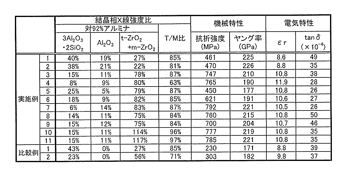
比較例1及び2は、電気特性が良好で、ヤング率も240GPa以下で良好であったが、曲げ強度(抗折強度)が303MPa以下で、強度が低かった。これは、Al2O3の強度比Pc/Paが0%で、Al2O3の結晶相が析出していなかったことが原因と考えられる。特に、比較例1は曲げ強度が230MPaと最も低かった。これは、3Al2O3・2SiO2の強度比Pb/Paが43%と高いことから、ガラス成分が多く、しかも、ZrO2の強度比が27%と低いことから、強度を高めることができなかったものと考えられる。
これに対して、実施例1~11は、誘電正接が、1MHzにおいて、50×10-4以下、比誘電率が7~13であり、電気特性が良好であった。しかも、曲げ強度が450MPa以上900MPa以下、ヤング率が170GPa以上240GPa以下であり、機械特性も良好であった。これは、Al2O3の強度比Pc/Paが5~25%であって、Al2O3の結晶相が析出しているからであると考えられる。特に、実施例7は曲げ強度が792MPaと最も高かった。これは、3Al2O3・2SiO2の強度比Pb/Paが6%と最も低く(ガラス成分が少なく)、Al2O3の強度比Pc/Paが14%と高く、しかも、ZrO2の強度比が83%と高いことから、強度を高めることができたものと考えられる。
また、実施例1及び2の結果から、3Al2O3・2SiO2の強度比Pb/Paが35%以上であっても、Al2O3の強度比Pc/Paが15%以上、ZrO2の強度比が20%以上あれば、曲げ強度450MPa以上を実現することができることがわかる。
実施例4の結果から、Al2O3の強度比Pc/Paが低くても、3Al2O3・2SiO2の強度比Pb/Paが低く、ZrO2の強度比が70%以上あれば、曲げ強度750MPa以上を実現することができることがわかる。
実施例9~11の結果から、3Al2O3・2SiO2の強度比Pb/Paが15%程度、Al2O3の強度比Pc/Paが10%程度であっても、ZrO2の強度比が100%を超える程度に高ければ、曲げ強度700MPa以上を実現することができることがわかる。
なお、本発明に係るセラミック素地及びその製造方法は、上述の実施の形態に限らず、本発明の要旨を逸脱することなく、種々の構成を採り得ることはもちろんである。
Claims (14)
- 結晶相が、3Al2O3・2SiO2を主結晶相とし、その他、Al2O3及びZrO2を含むことを特徴とするセラミック素地。
- 請求項1記載のセラミック素地において、
92%以上のAl2O3を含むセラミック基板のX線回折結果における(113)面のピーク強度をPa、
当該セラミック素地のX線回折結果における3Al2O3・2SiO2の(240)面のピーク強度をPbとしたとき、
前記ピーク強度Paに対する前記ピーク強度Pbの比(Pb/Pa)が5~50%であることを特徴とするセラミック素地。 - 請求項1記載のセラミック素地において、
92%以上のAl2O3を含むセラミック基板のX線回折結果における(113)面のピーク強度をPa、
当該セラミック素地のX線回折結果におけるAl2O3の(113)面のピーク強度をPcとしたとき、
前記ピーク強度Paに対する前記ピーク強度Pcの比(Pc/Pa)が5~25%であることを特徴とするセラミック素地。 - 請求項1記載のセラミック素地において、
92%以上のAl2O3を含むセラミック基板のX線回折結果における(113)面のピーク強度をPa、
当該セラミック素地のX線回折結果におけるt-ZrO2の(111)面のピーク強度をPt、m-ZrO2の(/111)面のピーク強度をPm1、m-ZrO2の(111)面のピーク強度をPm2としたとき、
前記ピーク強度Paに対する前記ピーク強度Pt、Pm1及びPm2の合計の比{(Pt+Pm1+Pm2)/Pa)}が15~200%であることを特徴とするセラミック素地。

- 請求項1記載のセラミック素地において、
AlをAl2O3換算で40.0~70.0質量%、ZrをZrO2換算で5.0~40.0質量%、SiをSiO2換算で10.0~30.0質量%、MnをMnO換算で2.0~8.0質量%を含むことを特徴とするセラミック素地。 - 請求項5記載のセラミック素地において、
Ba、Ti、Y、Ca及びMgのうち、少なくとも1種の元素を含み、
Al2O3、ZrO2、SiO2及びMnOの合計を100質量%としたとき、
Baを含む場合は、BaO換算で1.5質量%以下含み、
Tiを含む場合は、TiO2換算で1.5質量%以下含み、
Yを含む場合は、Y2O3換算で1.5質量%以下含み、
Caを含む場合は、CaO換算で1.5質量%以下含み、
Mgを含む場合は、MgO換算で1.5質量%以下含むことを特徴とするセラミック素地。 - 請求項1記載のセラミック素地において、
温度1200~1400℃にて焼結されていることを特徴とするセラミック素地。 - 請求項1記載のセラミック素地において、
曲げ強度が450Ma以上、ヤング率が240GPa以下であることを特徴とするセラミック素地。 - 請求項1記載のセラミック素地において、
曲げ強度が450MPa以上900MPa以下、ヤング率が170GPa以上240GPa以下であることを特徴とするセラミック素地。 - 請求項1記載のセラミック素地において、
誘電正接が、1MHzにおいて、50×10-4以下であり、比誘電率が7~13であることを特徴とするセラミック素地。 - AlをAl2O3換算で40.0~70.0質量%、ZrをZrO2換算で5.0~40.0質量%、SiをSiO2換算で10.0~30.0質量%、MnをMnO換算で2.0~8.0質量%を含有する成形体を作製する成形体作製工程と、
前記成形体を1200~1400℃にて焼成する焼成工程とを備えることを特徴とするセラミック素地の製造方法。 - 請求項11記載のセラミック素地の製造方法において、
前記成形体は、Ba、Ti、Y、Ca及びMgのうち、少なくとも1種の元素を含み、
Al2O3、ZrO2、SiO2及びMnOの合計を100質量%としたとき、
Baを含む場合は、BaO換算で1.5質量%以下含み、
Tiを含む場合は、TiO2換算で1.5質量%以下含み、
Yを含む場合は、Y2O3換算で1.5質量%以下含み、
Caを含む場合は、CaO換算で1.5質量%以下含み、
Mgを含む場合は、MgO換算で1.5質量%以下含むことを特徴とするセラミック素地の製造方法。 - 請求項11記載のセラミック素地の製造方法において、
前記成形体作製工程の後に、前記成形体に、金属を含む導体層を形成する工程をさらに備え、
前記焼成工程では、前記導体層が形成された成形体を焼成することを特徴とするセラミック素地の製造方法。 - 請求項11記載のセラミック素地の製造方法において、
前記焼成工程は、水素を5%以上含む、水素と窒素のフォーミングガス中で行うことを特徴とするセラミック素地の製造方法。
Priority Applications (2)
| Application Number | Priority Date | Filing Date | Title |
|---|---|---|---|
| CN201580070143.2A CN107108371B (zh) | 2014-12-26 | 2015-12-15 | 陶瓷基体及其制造方法 |
| JP2016566138A JP6640112B2 (ja) | 2014-12-26 | 2015-12-15 | セラミック素地及びその製造方法 |
Applications Claiming Priority (2)
| Application Number | Priority Date | Filing Date | Title |
|---|---|---|---|
| JP2014265037 | 2014-12-26 | ||
| JP2014-265037 | 2014-12-26 |
Publications (1)
| Publication Number | Publication Date |
|---|---|
| WO2016104251A1 true WO2016104251A1 (ja) | 2016-06-30 |
Family
ID=56150276
Family Applications (1)
| Application Number | Title | Priority Date | Filing Date |
|---|---|---|---|
| PCT/JP2015/085062 Ceased WO2016104251A1 (ja) | 2014-12-26 | 2015-12-15 | セラミック素地及びその製造方法 |
Country Status (3)
| Country | Link |
|---|---|
| JP (1) | JP6640112B2 (ja) |
| CN (1) | CN107108371B (ja) |
| WO (1) | WO2016104251A1 (ja) |
Citations (6)
| Publication number | Priority date | Publication date | Assignee | Title |
|---|---|---|---|---|
| JPH04182352A (ja) * | 1990-11-14 | 1992-06-29 | Tosoh Corp | 複合焼結体及びその製造方法 |
| JPH06166565A (ja) * | 1992-11-26 | 1994-06-14 | Kyocera Corp | ムライト質焼結体の製造方法 |
| JP2002137962A (ja) * | 2000-10-24 | 2002-05-14 | Nitsukatoo:Kk | ムライト質焼結体からなる熱処理用部材 |
| JP2002316869A (ja) * | 2001-04-19 | 2002-10-31 | Nitsukatoo:Kk | 耐熱性ムライト質焼結体からなるローラハースキルン用ローラ |
| JP2012137345A (ja) * | 2010-12-25 | 2012-07-19 | Kyocera Corp | プローブカード用セラミック配線基板およびこれを用いたプローブカード |
| JP2012138432A (ja) * | 2010-12-25 | 2012-07-19 | Kyocera Corp | プローブカード用セラミック配線基板 |
Family Cites Families (1)
| Publication number | Priority date | Publication date | Assignee | Title |
|---|---|---|---|---|
| JP5368053B2 (ja) * | 2008-10-15 | 2013-12-18 | 日本特殊陶業株式会社 | 多層セラミック基板及びその製造方法 |
-
2015
- 2015-12-15 CN CN201580070143.2A patent/CN107108371B/zh active Active
- 2015-12-15 WO PCT/JP2015/085062 patent/WO2016104251A1/ja not_active Ceased
- 2015-12-15 JP JP2016566138A patent/JP6640112B2/ja active Active
Patent Citations (6)
| Publication number | Priority date | Publication date | Assignee | Title |
|---|---|---|---|---|
| JPH04182352A (ja) * | 1990-11-14 | 1992-06-29 | Tosoh Corp | 複合焼結体及びその製造方法 |
| JPH06166565A (ja) * | 1992-11-26 | 1994-06-14 | Kyocera Corp | ムライト質焼結体の製造方法 |
| JP2002137962A (ja) * | 2000-10-24 | 2002-05-14 | Nitsukatoo:Kk | ムライト質焼結体からなる熱処理用部材 |
| JP2002316869A (ja) * | 2001-04-19 | 2002-10-31 | Nitsukatoo:Kk | 耐熱性ムライト質焼結体からなるローラハースキルン用ローラ |
| JP2012137345A (ja) * | 2010-12-25 | 2012-07-19 | Kyocera Corp | プローブカード用セラミック配線基板およびこれを用いたプローブカード |
| JP2012138432A (ja) * | 2010-12-25 | 2012-07-19 | Kyocera Corp | プローブカード用セラミック配線基板 |
Also Published As
| Publication number | Publication date |
|---|---|
| JP6640112B2 (ja) | 2020-02-05 |
| JPWO2016104251A1 (ja) | 2017-10-05 |
| CN107108371A (zh) | 2017-08-29 |
| CN107108371B (zh) | 2020-09-29 |
Similar Documents
| Publication | Publication Date | Title |
|---|---|---|
| JP6609622B2 (ja) | 配線基板 | |
| JP5645136B2 (ja) | 誘電体磁器組成物、多層誘電体基板、電子部品、及び誘電体磁器組成物の製造方法 | |
| JP6632995B2 (ja) | セラミック素地及びその製造方法 | |
| JP5902292B2 (ja) | セラミック素地及びその製造方法 | |
| JP6406646B2 (ja) | セラミックパッケージ及び電子部品 | |
| JP6314292B1 (ja) | セラミック素地及びその製造方法 | |
| JP6573872B2 (ja) | セラミック素地及びその製造方法 | |
| CN109565939A (zh) | 陶瓷基板和电子部件内置模块 | |
| CN109644559A (zh) | 电子器件以及多层陶瓷基板 | |
| JP6581967B2 (ja) | セラミック素地及びその製造方法 | |
| JP6640112B2 (ja) | セラミック素地及びその製造方法 | |
| JP6195479B2 (ja) | 多層セラミック基板およびその製造方法 | |
| JP2005145722A (ja) | 酸化物セラミックの製造方法およびこれを用いたセラミック多層基板の製造方法およびパワーアンプモジュール | |
| JP5675389B2 (ja) | プローブカード用配線基板およびプローブカード | |
| JP5648682B2 (ja) | 金属ベース基板 | |
| JPWO2011122406A1 (ja) | 金属ベース基板およびその製造方法 |
Legal Events
| Date | Code | Title | Description |
|---|---|---|---|
| 121 | Ep: the epo has been informed by wipo that ep was designated in this application |
Ref document number: 15872820 Country of ref document: EP Kind code of ref document: A1 |
|
| ENP | Entry into the national phase |
Ref document number: 2016566138 Country of ref document: JP Kind code of ref document: A |
|
| NENP | Non-entry into the national phase |
Ref country code: DE |
|
| 122 | Ep: pct application non-entry in european phase |
Ref document number: 15872820 Country of ref document: EP Kind code of ref document: A1 |