WO2016104046A1 - 透明導電性フィルム - Google Patents
透明導電性フィルム Download PDFInfo
- Publication number
- WO2016104046A1 WO2016104046A1 PCT/JP2015/083339 JP2015083339W WO2016104046A1 WO 2016104046 A1 WO2016104046 A1 WO 2016104046A1 JP 2015083339 W JP2015083339 W JP 2015083339W WO 2016104046 A1 WO2016104046 A1 WO 2016104046A1
- Authority
- WO
- WIPO (PCT)
- Prior art keywords
- transparent conductive
- film
- layer
- optical adjustment
- conductive thin
- Prior art date
- Legal status (The legal status is an assumption and is not a legal conclusion. Google has not performed a legal analysis and makes no representation as to the accuracy of the status listed.)
- Ceased
Links
Images


Classifications
-
- H—ELECTRICITY
- H01—ELECTRIC ELEMENTS
- H01B—CABLES; CONDUCTORS; INSULATORS; SELECTION OF MATERIALS FOR THEIR CONDUCTIVE, INSULATING OR DIELECTRIC PROPERTIES
- H01B5/00—Non-insulated conductors or conductive bodies characterised by their form
- H01B5/14—Non-insulated conductors or conductive bodies characterised by their form comprising conductive layers or films on insulating-supports
-
- G—PHYSICS
- G06—COMPUTING OR CALCULATING; COUNTING
- G06F—ELECTRIC DIGITAL DATA PROCESSING
- G06F3/00—Input arrangements for transferring data to be processed into a form capable of being handled by the computer; Output arrangements for transferring data from processing unit to output unit, e.g. interface arrangements
- G06F3/01—Input arrangements or combined input and output arrangements for interaction between user and computer
- G06F3/03—Arrangements for converting the position or the displacement of a member into a coded form
- G06F3/041—Digitisers, e.g. for touch screens or touch pads, characterised by the transducing means
-
- C—CHEMISTRY; METALLURGY
- C23—COATING METALLIC MATERIAL; COATING MATERIAL WITH METALLIC MATERIAL; CHEMICAL SURFACE TREATMENT; DIFFUSION TREATMENT OF METALLIC MATERIAL; COATING BY VACUUM EVAPORATION, BY SPUTTERING, BY ION IMPLANTATION OR BY CHEMICAL VAPOUR DEPOSITION, IN GENERAL; INHIBITING CORROSION OF METALLIC MATERIAL OR INCRUSTATION IN GENERAL
- C23C—COATING METALLIC MATERIAL; COATING MATERIAL WITH METALLIC MATERIAL; SURFACE TREATMENT OF METALLIC MATERIAL BY DIFFUSION INTO THE SURFACE, BY CHEMICAL CONVERSION OR SUBSTITUTION; COATING BY VACUUM EVAPORATION, BY SPUTTERING, BY ION IMPLANTATION OR BY CHEMICAL VAPOUR DEPOSITION, IN GENERAL
- C23C14/00—Coating by vacuum evaporation, by sputtering or by ion implantation of the coating forming material
- C23C14/06—Coating by vacuum evaporation, by sputtering or by ion implantation of the coating forming material characterised by the coating material
- C23C14/08—Oxides
Definitions
- the present invention relates to a transparent conductive film.
- a transparent conductive film in which a transparent conductive layer is laminated on one main surface of a transparent film base material is known.
- Transparent conductive films are widely used in devices such as touch panels.
- a fine wiring pattern is generated on the transparent conductive layer by photolithography, developed, and then subjected to wet etching to form a fine wiring pattern.
- the etching rate of the transparent conductive layer is too high, a wiring pattern cannot be formed with high accuracy due to problems such as side etching of fine wiring.
- the etching rate of the transparent conductive layer is too slow, the productivity of the patterning process decreases.
- Patent Document 1 Japanese Patent No. 5425351
- an optical adjustment layer (IM layer: Index Matching Layer) is formed between the film substrate and the transparent conductive layer, making the wiring pattern of the transparent conductive layer difficult to see.
- IM layer Index Matching Layer
- Patent Document 2 JP 2012-1114070.
- a wet optical adjustment layer formed by a wet method and a dry optical adjustment layer formed by a dry method are known as an optical adjustment layer.
- the wet optical adjustment layer dissolves a thermosetting resin composed of a mixture of a melamine resin, an alkyd resin, and an organic silane condensate in an organic solvent, coats the film substrate, and performs a curing process (for example, a heating process). Is formed.
- the dry optical adjustment layer is formed, for example, by depositing an inorganic oxide such as silicon oxide (SiO 2 ) or aluminum oxide (Al 2 O 3 ) on a film substrate by a sputtering method or the like.
- an inorganic oxide such as silicon oxide (SiO 2 ) or aluminum oxide (Al 2 O 3 )
- FIG. 3 shows a schematic diagram of a conventional transparent conductive film 30.
- the transparent film base material 31 the wet optical adjustment layer 32, and the transparent conductive layer 33 are laminated
- the wet optical adjustment layer 32 Since the wet optical adjustment layer 32 has a low film density and low hardness, there is a drawback that the scratch resistance of the transparent conductive film 30 is low.
- the dry optical adjustment layer (not shown) is characterized in that it tends to have a higher film density and higher hardness than the wet optical adjustment layer 32 and is excellent in scratch resistance of the transparent conductive film.
- the wiring of the transparent conductive layer is miniaturized, there is a high possibility that the wiring is disconnected even with a minute scratch. Therefore, the use of a dry optical adjustment layer with high scratch resistance in place of the wet optical adjustment layer 32 with low scratch resistance is increasing.
- the transparent conductive layer When a transparent conductive layer is formed on the wet optical adjustment layer, the transparent conductive layer can be etched at an appropriate rate. However, when a transparent conductive layer is formed on the dry optical adjustment layer, the etching rate of the transparent conductive layer becomes slow, and the productivity of the patterning process may be reduced. That is, the wet optical adjustment layer is excellent from the viewpoint of the etching property of the transparent conductive layer. However, the dry optical adjustment layer is excellent from the viewpoint of scratch resistance. Conventionally, a transparent conductive film having a dry optical adjustment layer with high scratch resistance and an appropriate etching rate of the transparent conductive layer has not been known.
- An object of the present invention is to realize a transparent conductive film including an optical adjustment layer including a dry optical adjustment layer from the viewpoint of scratch resistance and having an appropriate etching rate of the transparent conductive layer.
- the inventor of the present application controls the etching rate of the transparent conductive layer to an appropriate range by appropriately controlling the crystal orientation of the transparent conductive layer even if the optical adjustment layer includes the dry optical adjustment layer.
- the present invention has been completed by finding out what can be done.
- the transparent conductive film of the present invention is formed by laminating at least an optical adjustment layer and a transparent conductive layer in this order on at least one main surface of a transparent film substrate.
- the optical adjustment layer includes a dry optical adjustment layer containing an inorganic oxide.
- the transparent conductive layer contains a metal oxide containing indium.
- the transparent conductive layer is crystalline and has an X-ray diffraction peak corresponding to at least the (400) plane and the (440) plane.
- the ratio I 440 / I 400 of the X-ray diffraction peak intensity is 1.0-2. .2 range.
- the transparent conductive film of the present invention is formed by laminating at least an optical adjustment layer and a transparent conductive layer in this order on at least one main surface of a transparent film substrate.
- the optical adjustment layer includes a dry optical adjustment layer containing an inorganic oxide.
- the transparent conductive layer contains a metal oxide containing indium.
- the transparent conductive layer is crystalline and has an X-ray diffraction peak corresponding to at least the (222) plane, (400) plane, and (440) plane.
- the X-ray diffraction peak intensity of the (222) plane is I 222
- the X-ray diffraction peak intensity of the (400) plane is I 400
- the X-ray diffraction peak intensity of the (440) plane is I 440
- X-ray diffraction The peak intensity ratio I 400 / I 222 is in the range of 0.10 to 0.26
- the X-ray diffraction peak intensity ratio I 440 / I 400 is in the range of 1.0 to 2.2.
- the dry optical adjustment layer includes an inorganic oxide region having a carbon atom content of 0.2 atomic% or less in the thickness direction.
- the transparent conductive layer is a transparent conductive thin film laminate comprising a laminate of two or more transparent conductive thin films. All the transparent conductive thin films contain at least one impurity metal element in addition to indium.
- the transparent conductive thin film located farthest from the film substrate is the first transparent conductive thin film
- the content ratio of the impurity metal element to indium in the first transparent conductive thin film is determined by the transparent conductive thin film laminate. It is not the maximum in the content ratio of the impurity metal element to indium in all the transparent conductive thin films to be formed.
- the content ratio of the impurity metal element to indium in the first transparent conductive thin film is It is smaller than the content ratio of the impurity metal element to indium of the second transparent conductive thin film.
- the content ratio of the impurity metal element to indium in this application, expressed as the ratio of atomic number N D of the impurity metal elements for atomic N P of indium element in the transparent conductive layer "N D / N P ' .
- the content ratio of tin to indium in the indium tin oxide is represented by a ratio “N Sn / N In ” of the number of tin elements N Sn to the number of indium elements N In in the transparent conductive thin film.
- the content ratio of the impurity metal element to indium in the first transparent conductive thin film is such that the impurity metal element to indium in all the transparent conductive thin films constituting the transparent conductive thin film laminate. It is the smallest in the content ratio of.
- the content ratio of the impurity metal element to indium in the first transparent conductive thin film is 0.004 or more and less than 0.05.
- the transparent conductive thin film excluding the first transparent conductive thin film is an impurity metal element for indium. Is not less than 0.05 and not more than 0.16.
- the thickness of the first transparent conductive thin film is other than the first transparent conductive thin film. Less than the thickness of all transparent conductive thin films.
- the impurity metal element is made of tin (Sn).
- the optical adjustment layer includes a dry optical adjustment layer having high scratch resistance, but the transparent conductive film has an appropriate etching rate of the transparent conductive layer, that is, the transparent conductive film having both scratch resistance and etching property. The film was realized.
- FIG. 1 is a schematic view of a transparent conductive film 10 according to the first embodiment of the present invention.
- the optical adjustment layer 12 includes an inorganic oxide layer (dry optical adjustment layer) formed by a dry film formation method.
- the transparent conductive layer 13 contains a metal oxide containing indium.
- the transparent conductive layer 13 is crystalline and includes a crystal structure having an X-ray diffraction peak corresponding to at least the (400) plane and the (440) plane.
- the ratio of X-ray diffraction peak intensity I 440 / I 400 is 1.0-2. .2 range.
- the transparent conductive layer 13 further includes a crystal structure having an X-ray diffraction peak corresponding to the (222) plane, where the X-ray diffraction peak intensity of the (222) plane is I 222 .
- the ratio I 400 / I 222 is in the range of 0.10 to 0.26.
- the film substrate is made of a polymer film such as polyethylene terephthalate, polyethylene naphthalate, polyolefin, polycycloolefin, polycarbonate, polyether sulfone, polyarylate, polyimide, polyamide, polystyrene, norbornene.
- the material of the film substrate is not limited to these, but polyethylene terephthalate (PET) having excellent transparency, heat resistance, and mechanical properties is particularly preferable.
- the thickness of the film substrate is preferably 20 ⁇ m or more and 300 ⁇ m or less, but is not limited thereto. However, if the thickness of the film substrate is less than 20 ⁇ m, handling may be difficult. When the thickness of the film substrate exceeds 300 ⁇ m, there is a concern that the transparent conductive film is too thick when mounted on a touch panel or the like.
- an adhesive layer on the surface of the film base on the side of the transparent conductive layer and the surface on the opposite side thereof, an adhesive layer, an undercoat layer, an antiblocking layer, an oligomer prevention layer, a hard coat layer, etc.
- a functional layer may be provided.
- the easy-adhesion layer has a function of improving the adhesion between the film substrate and a layer (for example, an optical adjustment layer) formed on the film substrate.
- the undercoat layer has a function of adjusting the reflectance and optical hue of the film substrate.
- the anti-blocking layer has a function of suppressing pressure-bonding (blocking) caused by winding the transparent conductive film.
- the oligomer prevention layer has a function of suppressing low molecular weight components that precipitate when a film substrate (for example, a PET film substrate) is heated.
- the hard coat layer has a function of improving the scratch resistance of the transparent conductive film.
- the functional layer is preferably composed of a composition containing an organic resin.
- An optical adjustment layer is a layer for refractive index adjustment provided between a film base material and a transparent conductive layer.
- the optical characteristics for example, reflection characteristics
- the optical adjustment layer reduces the difference in reflectance between the portion with the wiring pattern of the transparent conductive layer and the portion without the wiring pattern, so that the wiring pattern of the transparent conductive layer becomes difficult to see (the wiring pattern of the transparent conductive layer is visually recognized). Is not desirable).
- the optical adjustment layer includes a dry optical adjustment layer (not shown) composed of a dry vapor deposition film formed by a dry film formation method such as a sputtering method, a vacuum vapor deposition method, or a CVD method.
- the dry optical adjustment layer includes an inorganic oxide layer, and preferably includes an inorganic oxide layer.
- the manufacturing method of a dry optical adjustment layer will not be specifically limited if it is a dry-type film-forming method with which sufficient abrasion resistance is acquired, It is not limited to the sputtering method mentioned above, a vacuum evaporation method, and CVD method.
- Vacuum deposition, sputtering, ion plating, and the like are sometimes referred to as “physical vapor deposition”, and CVD is sometimes referred to as “chemical vapor deposition”.
- a dry optical adjustment layer containing an inorganic oxide formed by a dry film formation method becomes a “dry optical adjustment layer comprising a vapor deposition layer containing an inorganic oxide”.
- the optical adjustment layer may have a multilayer structure of a wet optical adjustment layer and a dry optical adjustment layer. Since the optical adjustment layer including the dry optical adjustment layer includes a layer having a high hardness (dry optical adjustment layer), the scratch resistance of the transparent conductive film is increased. Moreover, since the optical adjustment layer includes a dry optical adjustment layer including an inorganic oxide layer, the optical adjustment layer has gas barrier properties. Therefore, film quality deterioration of the transparent conductive layer due to gas (for example, moisture) generated from the film substrate can be prevented.
- gas for example, moisture
- the dry optical adjustment layer is preferably laminated on the wet optical adjustment layer (on the transparent conductive layer side).
- the wet optical adjustment layer may contain a large amount of gas (for example, gas derived from an organic solvent), and may cause film quality deterioration of the transparent conductive layer.
- the optical adjustment layer has a multilayer structure of a wet optical adjustment layer and a dry optical adjustment layer, more preferably, the dry optical adjustment layer is laminated on the wet optical adjustment layer, and the dry optical adjustment layer is a transparent conductive layer. Adjacent to each other.
- the constituent material of the dry optical adjustment layer is not particularly limited.
- silicon oxide silicon monoxide (SiO), silicon dioxide (SiO 2 ) (usually called silicon oxide), silicon oxide (SiOx: x is 1). And less than 2)
- aluminum oxide Al 2 O 3
- zirconium oxide ZrO 2
- niobium oxide Nb 2 O 5
- titanium oxide TiO 2
- the composition of the inorganic oxide may be a stoichiometric composition or a non-stoichiometric composition.
- the dry optical adjustment layer may be a composite layer in which an inorganic oxide layer having a stoichiometric composition and an inorganic oxide layer having a non-stoichiometric composition are laminated.
- the dry optical adjustment layer may be a single inorganic oxide layer or a laminate of inorganic oxide layers in which a plurality of inorganic oxide layers having different inorganic elements are laminated. Since the optical adjustment layer including the dry optical adjustment layer has higher scratch resistance than the wet optical adjustment layer, the transparent conductive layer has higher scratch resistance than when the optical adjustment layer does not include the dry optical adjustment layer.
- the dry optical adjustment layer is preferably laminated adjacent to the transparent conductive layer. Since the dry optical adjustment layer is laminated in contact with the transparent conductive layer, the dry optical adjustment layer having high hardness has a structure that directly supports the transparent conductive layer, so that the scratch resistance of the transparent conductive layer is further increased.
- the thickness of the optical adjustment layer is not necessarily limited, but is, for example, 2 nm or more, preferably 5 nm or more, more preferably 10 nm or more, and, for example, 100 nm or less, preferably 80 nm. Or less, more preferably 60 nm or less. If the thickness of the optical adjustment layer is less than 2 nm, the scratch resistance may be insufficient. When the thickness of the optical adjustment layer exceeds 100 nm, the flex resistance of the transparent conductive film may be deteriorated.
- the method for forming the inorganic oxide layer is not necessarily limited, but it is preferably formed by a sputtering method.
- a sputtered film formed by a sputtering method can stably obtain a particularly dense film even in a dry process. Therefore, an optical adjustment layer including an inorganic oxide layer formed by a sputtering method is, for example, a vacuum evaporation method. Compared to the optical adjustment layer formed in step 1, the scratch resistance is high.
- the sputtering method has a higher density of the film formed than, for example, a vacuum deposition method, a film having excellent gas barrier properties can be obtained.
- the film density of the inorganic oxide layer is preferably as high as possible.
- the film density of the inorganic oxide layer is made of silicon dioxide (SiO 2 )
- the film density is 2.1 g / cm 3 in order to reliably obtain scratch resistance and gas barrier properties.
- the above is preferable.
- the film density of the inorganic oxide layer can be determined by the X-ray reflectivity method.
- the pressure of the sputtering gas when forming the inorganic oxide layer there is no limitation on the pressure of the sputtering gas when forming the inorganic oxide layer, but for example, 0.09 Pa to 0.5 Pa is preferable, and 0.09 Pa to 0.3 Pa is more preferable.
- the pressure of the sputtering gas in the above range, a denser sputtered film can be formed, and good scratch resistance and gas barrier properties can be easily obtained.
- the pressure of the sputtering gas exceeds 0.5 Pa, a dense film may not be obtained.
- the pressure of the sputtering gas is less than 0.09 Pa, the discharge becomes unstable and there is a possibility that voids are formed in the inorganic oxide layer.
- the reactive sputtering method can be used to efficiently form the film.
- silicon (Si) is used as a sputtering target
- argon is introduced as a sputtering gas
- oxygen is introduced as a reactive gas (introduction amount is, for example, 10 vol% to 80 vol% with respect to argon)
- a silicon oxide (for example, silicon dioxide (SiO 2 )) film having high scratch resistance and gas barrier properties can be obtained.
- the reason why the etching rate of the transparent conductive layer is slow is not limited to any theory. Is estimated as follows.
- the optical adjustment layer is a wet optical adjustment layer, even if the transparent conductive layer is subjected to a heat crystallization treatment (for example, 140 ° C., 60 minutes), the transparent conductive layer on the film substrate side (for example, The region having a thickness of about 3 nm adjacent to the wet optical adjustment layer is less likely to have a stable crystal structure due to the gas (for example, moisture) derived from the film substrate and the wet optical adjustment layer, and is relatively amorphous. Close structure.
- the etching rate of amorphous is extremely high, so the transparent conductive layer is etched from the surface side (the side opposite to the film substrate) toward the film substrate side It is considered that the etching rate becomes faster as it is done.
- the optical adjustment layer includes a dry optical adjustment layer, since the dry optical adjustment layer has gas barrier properties, it is not affected by the gas derived from the film substrate. Therefore, the transparent conductive layer can obtain a uniform crystalline throughout the thickness direction. As a result, there is no change in the etching rate in the thickness direction of the transparent conductive layer, and as a result, the etching rate is considered to be slow.
- the dry optical adjustment layer constituting the optical adjustment layer is an impurity atom (representative) other than an inorganic atom (eg, silicon atom) and an oxygen atom constituting an inorganic oxide (eg, silicon dioxide) in the thickness direction.
- an impurity atom representedative
- an inorganic atom eg, silicon atom
- an oxygen atom constituting an inorganic oxide (eg, silicon dioxide) in the thickness direction.
- the carbon atoms are derived from, for example, a film base material or a wet hard coat layer formed on the film base material by a wet method.
- the wet optical adjustment layer may contain carbon atoms derived from an organic resin.
- the presence or absence of a region having carbon atoms of 0.2 atomic% or less is determined by performing a depth profile measurement by X-ray photoelectron spectroscopy (ESCA: Electron Spectroscopy for Chemical Analysis).
- Carbon atoms lower the film density of the dry optical adjustment layer and cause a decrease in scratch resistance of the transparent conductive film.
- the optical adjustment layer has a region having carbon atoms of 0.2 atomic% or less (substantially free of carbon atoms) in the thickness direction, sufficient scratch resistance of the transparent conductive film can be obtained.
- the ratio in the thickness direction of the region where the carbon atom content is 0.2 atomic% or less is, for example, 10% or more, preferably 15%. Or more, more preferably 20% or more, still more preferably 25% or more, and most preferably 30% or more.
- the “region where the carbon atom is 0.2 atomic% or less” is obtained by X-ray photoelectron spectroscopy, and details of how to obtain it are described in the [Evaluation of carbon atom content and existence region of optical adjustment layer] column.
- the ratio in the thickness direction of the region where carbon atoms are 0.2 atomic% or less is the thickness A (nm) of the dry optical adjustment layer and the thickness B (nm) of the region where the carbon atoms are detected in the dry optical adjustment layer. ) And calculating the formula “100- (B / A) X100” (unit:%). Sufficient scratch resistance can be obtained if the ratio in the thickness direction of the region having carbon atoms of 0.2 atomic% or less is 10% or more. The higher the ratio in the thickness direction of the region where the carbon atom is 0.2 atomic% or less, the better, but there is an analytical limit.
- the carbon atoms constituting the film substrate in the vicinity of the film substrate of the optical adjustment layer As a result, an analysis result of 100% cannot be obtained.
- the upper limit value of the ratio in the thickness direction of the region having carbon atoms of 0.2 atomic% or less is, for example, 90%.
- the dry optical adjustment layer containing no impurity atoms (typically carbon atoms)
- the dry optical adjustment layer is less likely to contain impurity atoms (typically carbon atoms). It becomes easy to obtain a dry optical adjustment layer having a high density.
- the transparent conductive layer is a layer containing a metal oxide containing indium, that is, a transparent thin film layer containing indium oxide as a main component, or a composite metal oxide containing indium and one or more impurity metal elements as a main component. Includes a transparent thin film layer.
- the constituent material of the transparent conductive layer is not particularly limited as long as the transparent conductive layer includes a layer containing indium, has light transmittance in a visible light region, and has conductivity.
- the transparent conductive layer is preferably made of a metal oxide containing indium.
- indium oxide indium tin oxide
- ITO Indium Tin Oxide
- IGZO indium gallium Zinc Oxide
- ITO Indium Tin Oxide
- ITO Indium Tin Oxide
- one or more impurity metal elements contained in the transparent conductive layer is tin (Sn), and indium gallium zinc oxide (IGZO: Indium Gallium Zinc Oxide) ) Is gallium (Ga) and zinc (Zn).
- the transparent conductive layer further contains an optional metal element, for example, an impurity metal element such as titanium (Ti), magnesium (Mg), aluminum (Al), gold (Au), silver (Ag), or copper (Cu). It may be.
- the transparent conductive layer is formed on the optical adjustment layer by sputtering, vapor deposition or the like, but the production method is not limited to this.
- the transparent conductive layer contains one or more impurity metal elements in addition to indium, such as indium tin oxide (ITO), the content ratio of the impurity metal element to indium is in the range of 0.004 to 0.16.
- ITO indium tin oxide
- the content ratio of the impurity metal element to indium is determined based on the content of tin oxide.
- the weight is approximately 0.5 wt% or more and 15 wt% or less, 3 wt% or more and 15 wt% or less, and 9 wt%, respectively. % To 12.5% by weight.
- the “content ratio of impurity metal oxide” in the present application refers to the weight ratio (percentage) of the impurity metal oxide to the total weight of indium oxide and impurity metal oxide.
- a transparent conductive layer (for example, an indium tin oxide (ITO) layer) formed at a low temperature is amorphous and can be converted from amorphous to crystalline by heat treatment.
- the transparent conductive layer has a low surface resistance value when converted to crystalline.
- the conditions for converting the transparent conductive layer to crystalline are preferably, for example, a temperature of 140 ° C. and a time of 90 minutes or less from the viewpoint of productivity.
- the transparent conductive layer is crystalline or not can be confirmed by performing planar TEM observation using a transmission electron microscope (TEM: Electron Microscope).
- TEM Transmission electron microscope
- the transparent conductive layer is made of indium tin oxide (ITO)
- the transparent conductive layer is immersed in hydrochloric acid (concentration 5% by weight) at 20 ° C. for 15 minutes, washed with water, dried, and then 15 mm in length. It can also be determined whether or not it is crystalline by measuring the resistance between two terminals. Since the amorphous indium tin oxide (ITO) film is etched away by hydrochloric acid and disappears, the resistance increases when immersed in hydrochloric acid. In this specification, an indium tin oxide (ITO) film is crystalline when the resistance between two terminals between 15 mm does not exceed 10 k ⁇ after immersion in hydrochloric acid, washing with water, and drying.
- the transparent conductive layer is crystalline and has an X-ray diffraction peak corresponding to at least the (400) plane and the (440) plane.
- the X-ray diffraction peak intensity of the (400) plane of the transparent conductive layer is I 400
- the X-ray diffraction peak intensity of the (440) plane is I 440
- the ratio of X-ray diffraction peak intensity I 440 / I 400 is For example, 1.0 or more, preferably 1.1 or more, more preferably 1.2 or more, for example, 2.2 or less, preferably 2.0 or less, More preferably, it is 1.9 or less, More preferably, it is 1.8 or less.
- the optical adjustment layer includes a dry optical adjustment layer. Nevertheless, the etching rate of the transparent conductive layer can be controlled within an appropriate range.
- the transparent conductive layer preferably has an X-ray diffraction peak corresponding to the (222) plane in addition to the X-ray diffraction peaks corresponding to the (400) plane and the (440) plane.
- the X-ray diffraction peak intensity ratio I 400 / I 222 is, for example, 0.10 or more, preferably 0.11 or more, more preferably 0.12 or more. In addition, for example, it is 0.26 or less, preferably 0.25 or less, more preferably 0.24 or less, still more preferably 0.22 or less, and most preferably 0.8. 21 or less.
- the etching rate of the transparent conductive layer can be controlled to an appropriate range.
- the X-ray diffraction peak intensity ratio I 440 / I 400 of the transparent conductive layer is more preferably in the range of 1.0 to 2.2, and the X-ray diffraction peak intensity ratio I 400 / I 222 is in the range of 0.10 to 0.26.
- the etching rate of the transparent conductive layer can be further controlled within an appropriate range.
- each X-ray diffraction peak intensity in this application shall use the value which subtracted the background.
- the reason why the ratio of the X-ray diffraction peak intensity (I 400 / I 222 and I 440 / I 400 ) is within the above range can control the etching rate of the transparent conductive layer to a suitable range is limited to any theory. Although not, it is estimated as follows.
- the transparent conductive layer may have different etching rates depending on the crystal orientation. Therefore, for example, when the transparent conductive layer has a polycrystalline orientation such as an indium tin oxide layer (ITO), it is considered that the etching rate can be adjusted to a suitable range by controlling the crystal orientation.
- ITO indium tin oxide layer
- the transparent conductive layer is not affected by the gas derived from the film base material, and a uniform crystalline material is obtained over the entire thickness direction. It is thought that the crystal orientation factor has a particularly great influence on the etching rate.
- the optical adjustment layer is composed of a wet optical adjustment layer, due to the influence of the gas of the film substrate and the wet optical adjustment layer, a part of the transparent conductive film on the film substrate side is similar to an amorphous material that is easily etched Since the film quality is obtained, the film quality factor on the film substrate side has a larger effect than the crystal orientation factor, and as a result, a suitable etching rate can be stably obtained.
- the means for adjusting the intensity of the X-ray diffraction peak of the transparent conductive layer is not particularly limited.
- the manufacturing conditions of the transparent conductive layer for example, the film formation pressure and the substrate temperature during film formation
- the film composition of the transparent conductive layer for example, the type and content ratio of the impurity metal element
- the film thickness or the film configuration
- the intensity of the X-ray diffraction peak corresponding to the (400) plane, (440) plane, or (222) plane is suitably changed by appropriately changing the layering of transparent conductive layers having different impurity metal element content ratios.
- the substrate temperature during film formation is preferably ⁇ 40 ° C. or higher and 180 ° C.
- the “substrate temperature at the time of film formation” is a set temperature of the base of the substrate at the time of sputtering film formation.
- the base material temperature in the case where the sputter film formation is continuously performed by the roll sputtering apparatus is the temperature of the film formation roll on which the sputter film formation is performed.
- the arithmetic surface roughness Ra of the transparent conductive layer is preferably 0.1 nm or more and 2.0 nm or less, and more preferably 0.1 nm or more and 1.5 nm or less. When the arithmetic surface roughness Ra exceeds 2.0 nm, the resistance value of the transparent conductive layer may be greatly increased. If the arithmetic surface roughness Ra is less than 0.1 nm, when the transparent conductive layer is formed by patterning wiring by photolithography, the adhesion between the photoresist and the transparent conductive layer may be lowered, and etching failure may occur.
- the specific resistance value of the transparent conductive layer is, for example, 4 ⁇ 10 ⁇ 4 ⁇ ⁇ cm or less, preferably 3.8 ⁇ 10 ⁇ 4 ⁇ ⁇ cm or less, and more preferably 3.3 ⁇ 10 ⁇ 4 ⁇ ⁇ cm or less. More preferably 3.0 ⁇ 10 ⁇ 4 ⁇ ⁇ cm or less, still more preferably 2.7 ⁇ 10 ⁇ 4 ⁇ ⁇ cm or less, and most preferably 2.4 ⁇ 10 ⁇ 4 ⁇ ⁇ cm or less. For example, it is 1 ⁇ 10 ⁇ 4 ⁇ ⁇ cm or more.
- a transparent conductive layer having a small specific resistance value tends to have a large crystal grain size and a slow etching rate. The tendency is particularly remarkable in the low specific resistance transparent conductive layer formed on the dry optical adjustment layer.
- the transparent conductive film of the present application controls the crystal orientation of the transparent conductive layer, and the X-ray diffraction peak intensity corresponding to the (400) plane, (440) plane, or (222) plane is controlled against etching. Therefore, a transparent conductive layer having a small specific resistance value can be suitably employed.
- the specific resistance value of the transparent conductive layer is the surface resistance value ( ⁇ / ⁇ ) of the transparent conductive layer measured by a four-terminal method according to JIS K7194 (1994), and the transparent conductive layer measured by a transmission electron microscope. It can be determined using the thickness of the layer.
- the film thickness of the transparent conductive layer is not necessarily limited, but is preferably 10 nm or more and 50 nm or less, more preferably 13 nm or more and 45 nm or less, further preferably 15 nm or more and 40 nm or less, and 15 nm or more and 35 nm or less. It is particularly preferred.
- the transparent conductive film can be particularly suitably applied to touch panel applications.
- the film thickness of the transparent conductive layer is less than 10 nm, it is difficult to be crystalline, and the surface resistance value of the transparent conductive layer may increase.
- the film thickness of the transparent conductive layer exceeds 50 nm, the optical characteristics (for example, light transmittance) of the transparent conductive film may be deteriorated, or the etching rate of the transparent conductive layer may be decreased.
- FIG. 2 is a schematic view of a transparent conductive film 20 according to the second embodiment of the present invention (the same reference numerals are used for elements common to the configuration of FIG. 1).
- the transparent conductive film 20 the transparent film base material 11, the optical adjustment layer 12, the 2nd transparent conductive thin film 15, and the 1st transparent conductive thin film 14 are laminated
- the transparent conductive layer includes a first transparent conductive thin film 14 and a second transparent conductive thin film 15, and the first transparent conductive thin film 14 and the second transparent conductive thin film 15 contain one or more impurity metal elements in addition to indium. .
- the optical adjustment layer 12 includes a dry optical adjustment layer including an inorganic oxide layer.
- the first transparent conductive thin film 14 and the second transparent conductive thin film 15 are both crystalline and include a crystal structure having X-ray diffraction peaks corresponding to at least the (400) plane and the (440) plane.
- the X-ray diffraction peak intensity of the (400) plane is I 400
- the X-ray diffraction peak intensity of the (440) plane is I 440
- the ratio of X-ray diffraction peak intensity I 440 / I 400 is 1.0-2. .2 range.
- the first transparent conductive thin film 14 and the second transparent conductive thin film 15 further include a crystal structure having an X-ray diffraction peak corresponding to the (222) plane, and has an X-ray diffraction peak intensity of the (222) plane.
- the X-ray diffraction peak intensity ratio I 400 / I 222 is in the range of 0.10 to 0.26.
- the content ratio of the impurity metal element to indium in the first transparent conductive thin film 14 and the second transparent conductive thin film 15 is preferably 0.004 or more and 0.16 or less, 0.01 or more, 0.15 Or less, more preferably 0.03 or more and 0.13 or less. If the content ratio of the impurity metal element to indium is less than 0.004, the surface resistance value of the transparent conductive layer may be remarkably increased, and if it exceeds 0.16, the uniformity of the surface resistance value in the plane of the transparent conductive layer May be lost.
- the indium tin oxide is used as the first transparent conductive thin film 14 and the second transparent conductive thin film 15, that is, when the main metal is indium and the impurity metal element is tin
- tin content percentage of SnO 2 weight with respect to the total weight of In 2 O 3 and SnO 2
- the content ratio of the impurity metal element to indium is more preferably 0.05 or more and 0.16 or less, and particularly preferably 0.06 or more and 0.16 or less. 0.09 or more and 0.13 or less is most preferable.
- the content ratio of the impurity metal element to indium is in the above range, a transparent conductive thin film having excellent low resistance characteristics can be obtained.
- the indium tin oxide is used as the second transparent conductive thin film 15, that is, when the main metal is indium and the impurity metal element is tin
- these content ratios are determined based on the tin oxide content (In 2 O 3
- the percentage of SnO 2 weight relative to the total weight of SnO 2 and SnO 2 is approximately 5% by weight, 15% by weight, 6% by weight, 15% by weight, 9% by weight, 12%, respectively. .5% by weight or less.
- the content ratio of the impurity metal element to indium is more preferably 0.004 or more and less than 0.05, and particularly preferably 0.01 or more and 0.04 or less. .
- a transparent conductive thin film having a high crystallization speed that can be crystallized by a short heat treatment for example, 140 ° C., 45 minutes
- a short heat treatment for example, 140 ° C., 45 minutes
- the content ratio ranges (In 2 When expressed as a percentage of the weight of SnO 2 with respect to the total weight of O 3 and SnO 2 , they are approximately 0.5 wt% or more, less than 5 wt%, 1 wt% or more, and 4 wt% or less, respectively.
- the content ratio of the impurity metal element to indium is 0.004 or more and 0.05 on the second transparent conductive thin film 15 whose content ratio of impurity metal element to indium is 0.05 or more and 0.16 or less.
- the first transparent conductive thin film 14 that is less than 1 a transparent conductive layer having a high crystallization speed and low resistance is obtained, and in addition, the ratio of the X-ray diffraction peak intensity of the transparent conductive layer ( I 400 / I 222 and I 440 / I 400 ) can be easily adjusted.
- the content ratio of the impurity metal element to indium in the first transparent conductive thin film 14 is smaller than the content ratio of the impurity metal element to indium in the second transparent conductive thin film 15.
- the transparent conductive thin film located farthest from the film substrate is the first transparent conductive thin film.
- the content ratio of the impurity metal element to indium in the first transparent conductive thin film is not the maximum among the content ratio of the impurity metal element to indium in all the transparent conductive thin films. That is, another transparent conductive thin film having a larger content ratio of impurity metal elements to indium than the first transparent conductive thin film is provided. More preferably, the content ratio of the impurity metal element to indium in the first transparent conductive thin film is the smallest among the content ratios of the impurity metal element to indium in all the transparent conductive thin films.
- a transparent conductive layer having a small content of impurity metal elements with respect to indium has a high resistance when crystallized, but is easily crystallized.
- a transparent conductive layer having a high content of impurity metal elements with respect to indium is difficult to crystallize, but has a low resistance when crystallized.
- the transparent conductive layer has a two-layer structure of a first transparent conductive thin film 14 with a small content ratio of impurity metal elements to indium and a second transparent conductive thin film 15 with a high content ratio of impurity metal elements to indium
- Crystallization of the entire transparent conductive layer is promoted by the transparent conductive thin film 14, and when the entire transparent conductive layer is crystallized, a film having a low resistance value is obtained by the second transparent conductive thin film 15.
- the thickness of the second transparent conductive thin film 15 is larger than the thickness of the first transparent conductive thin film 14.
- the first transparent conductive thin film has a lower content ratio of impurity metal elements to indium than the other transparent conductive thin films, and the first transparent conductive thin film
- the thickness is smaller than the conductive thin film, crystallization of the entire transparent conductive layer is promoted, and when the entire transparent conductive layer is crystallized, a film having a low resistance value is obtained.
- the thickness of the first transparent conductive thin film 14 is, for example, relative to the thickness of the transparent conductive layer (for example, in the case of a two-layer configuration, the total thickness of the first transparent conductive thin film 14 and the second transparent conductive thin film 15). , Less than 50%, preferably 45% or less, more preferably 40% or less, and even more preferably 30% or less.
- the transparent conductive film of Example 1 has a layer structure shown in FIG.
- the film substrate is a polyethylene terephthalate (PET) film having a thickness of 100 ⁇ m.
- the optical adjustment layer is made of a silicon oxide layer formed by sputtering and has a thickness of 20 nm.
- the first transparent conductive thin film comprises a first indium tin oxide (ITO) layer (thickness 3 nm), and the second transparent conductive thin film comprises a second indium tin oxide (ITO) layer (thickness 19 nm).
- the content ratio of tin (impurity metal element) to indium in the first indium tin oxide layer (first transparent conductive thin film) (the atomic ratio Sn / In number of Sn atoms to the number of In atoms) is 0.03.
- the content ratio of tin (impurity metal element) to indium in the 2 indium tin oxide layer (second transparent conductive thin film) (the atomic ratio Sn / In number of Sn atoms to the number of In atoms) is 0.10.
- a hard coat layer with a thickness of 0.3 ⁇ m is formed on the main surface of the 100 ⁇ m-thick polyethylene terephthalate film (Mitsubishi Resin) (the surface on the side where the optical adjustment layer is formed) made of an ultraviolet curable resin containing an acrylic resin. And it was set as the film base material.
- optical adjustment layer (and the first transparent conductive thin film and the second transparent conductive thin film described later) were formed using a roll-to-roll type sputtering apparatus.
- the roll of the film substrate was placed in the supply unit of the sputtering apparatus and stored for 15 hours in a vacuum state of 1 ⁇ 10 ⁇ 4 Pa or less. Thereafter, the film base material is fed out from the supply unit, and the back surface (the surface opposite to the hard coat layer surface) of the film base material is conveyed while being brought into contact with a film forming roll having a surface temperature of 0 ° C.
- An optical adjustment layer was formed on (on the hard coat layer).
- the film density of the obtained silicon oxide layer was evaluated by the X-ray reflectivity method, the film density was 2.2 g / cm 3 .
- Metal Mining Co., Ltd. was formed on a film substrate (on a hard coat layer) by sputtering using an alternating current / medium frequency (AC / MF) power source.
- a transparent conductive layer was formed following the optical adjustment layer.
- the transparent conductive layer was a transparent conductive thin film laminate having a two-layer structure of a second transparent conductive thin film and a first transparent conductive thin film.
- the film substrate on which the optical adjustment layer is formed is conveyed while contacting the back surface (the surface opposite to the optical adjustment layer) with a film forming roll having a surface temperature of 0 ° C.
- Indium content ratio Sn / In 0.03) was formed.
- An indium tin oxide target composed of a body was formed by sputtering using a magnet with a horizontal magnetic field of 30 mT and a direct current (DC) power source.
- An indium tin oxide target composed of a body was formed by sputtering using a magnet with a horizontal magnetic field of 30 mT and a direct current (DC) power source.
- crystallization treatment is performed by heating at 140 ° C. for 90 minutes in the atmosphere.
- the transparent conductive film of Example 1 provided with a crystalline transparent conductive layer was produced.
- Example 2 Example 1 except that the thickness of the first indium tin oxide layer (first transparent conductive thin film) was 6 nm and the thickness of the second indium tin oxide layer (second transparent conductive thin film) was 16 nm. Thus, a transparent conductive film of Example 2 was produced.
- Example 3 Example 1 except that the thickness of the first indium tin oxide layer (first transparent conductive thin film) was 8 nm and the thickness of the second indium tin oxide layer (second transparent conductive thin film) was 14 nm. Thus, a transparent conductive film of Example 3 was produced.
- Example 4 Example 1 except that the thickness of the first indium tin oxide layer (first transparent conductive thin film) was 4 nm and the thickness of the second indium tin oxide layer (second transparent conductive thin film) was 18 nm. Thus, a transparent conductive film of Example 4 was produced.
- Example 5 Example 1 except that a first indium tin oxide layer (first transparent conductive thin film) and a second indium tin oxide layer (second transparent conductive thin film) were formed using a magnet with a horizontal magnetic field of 100 mT. In the same manner as described above, a transparent conductive film of Example 5 was produced. By increasing the horizontal magnetic field from 30 mT to 100 mT, the specific resistance value of the transparent conductive layer is lowered.
- Comparative Example 1 The film configuration of the transparent conductive film of Comparative Example 1 is shown in FIG.
- the optical adjustment layer is a wet optical adjustment layer.
- the wet optical adjustment layer dissolves a thermosetting resin composed of a mixture of melamine resin, alkyd resin and organosilane condensate (melamine resin: alkyd resin: organosilane condensate weight ratio is 2: 2: 1) in an organic solvent. Then, after coating on a film substrate, it was formed by thermosetting.
- the thickness of the wet optical adjustment layer was 35 nm.
- the transparent conductive layer is composed of two layers of a first indium tin oxide layer and a second indium tin oxide layer, and the formation method thereof includes a thickness of the first indium tin oxide layer of 4 nm and a second indium tin oxide layer.
- a transparent conductive film of Comparative Example 1 was produced in the same manner as in Example 1 except that the thickness of was set to 18 nm.
- the transparent conductive film of Comparative Example 2 has one indium tin oxide layer, and the film configuration is the same as in FIG.
- a transparent conductive film of Comparative Example 2 was produced in the same manner as Example 1 except for this.
- the transparent conductive film of Comparative Example 3 has one indium tin oxide layer, and the film configuration is the same as in FIG.
- Table 1 shows the structures and properties of the transparent conductive films of Examples 1 to 5 and Comparative Examples 1 to 3 of the transparent conductive film of the present invention.
- the specific resistance values of the transparent conductive layers in the transparent conductive films of Examples 1 to 5 and Comparative Examples 1 to 3 are as in Examples 1 to 4 and Comparative Examples 1 to 3.
- the range was 3.2 ⁇ 10 ⁇ 4 ⁇ ⁇ cm to 3.6 ⁇ 10 ⁇ 4 ⁇ ⁇ cm, and in Example 5, it was confirmed to be 2.2 ⁇ 10 ⁇ 4 ⁇ ⁇ cm.
- the transparent conductive films of Examples 1 to 5 and Comparative Examples 1 to 3 since the transparent conductive layer is crystalline, the specific resistance value in the above range can be obtained. If it is the above-mentioned specific resistance value, the obtained transparent conductive film can be used conveniently for a touchscreen use etc.
- the optical adjustment layer (a silicon oxide layer having a thickness of 20 nm formed by a sputtering method) has a region having carbon atoms of 0.2 atomic% or less in the thickness direction. It was confirmed by X-ray photoelectron spectroscopy (ESCA: Electron Spectroscopy for Chemical Analysis). X-ray photoelectron spectroscopy shows that the wet optical adjustment layer (35 nm thick thermosetting resin layer formed by the coating method) in Comparative Example 1 does not have a region having carbon atoms of 0.2 atomic% or less in the thickness direction. It was confirmed by the law.
- ESA Electron Spectroscopy for Chemical Analysis
- the etching time of the transparent conductive layer of Comparative Example 1 provided with the wet optical adjustment layer was 60 seconds. Further, the etching time of the transparent conductive layers of Examples 1 to 5 provided with the dry optical adjustment layer was 90 to 100 seconds. Although the etching time of the transparent conductive layers of Examples 1 to 5 is longer than that of Comparative Example 1, it is 110 seconds or less, which is a pass ( ⁇ mark) level. The etching time of the transparent conductive layers of Comparative Examples 2 to 3 was 120 seconds to 130 seconds, which was a level of failure (marked by X).
- the 1st indium tin oxide layer (1st transparent conductive thin film) and the 2nd indium tin oxide layer (2nd transparent) were used using the magnet of a horizontal magnetic field of 100 mT.
- a transparent conductive film of a reference example having a crystalline transparent conductive layer was prepared in the same manner as in Comparative Example 1 except that the conductive thin film was formed.
- the specific resistance, etching time, and scratch resistance were evaluated in the same manner as in Examples and Comparative Examples. As a result, the specific resistance value was 2.1 ⁇ 10 ⁇ 4 ⁇ ⁇ cm, the etching time was 90 seconds, and the scratch resistance was “X”.
- Comparative Example 1 Comparing Comparative Example 1 with a wet optical adjustment layer and a reference example, the reference example has a smaller specific resistance value than Comparative Example 1 (specifically, Comparative Example 1 has 3.2 ⁇ 10 ⁇ 4 ⁇ ⁇ cm). 3.6 ⁇ 10 ⁇ 4 ⁇ ⁇ cm, whereas the reference example has 2.1 ⁇ 10 ⁇ 4 ⁇ ⁇ cm, and the etching time is slow (specifically, Comparative Example 1 has 60 seconds) In contrast, the reference example is 90 seconds).
- Comparative Example 1 has 3.2 ⁇ 10 ⁇ 4 ⁇ ⁇ cm
- the reference example has 2.1 ⁇ 10 ⁇ 4 ⁇ ⁇ cm
- the etching time is slow
- Comparative Example 1 has 60 seconds
- the reference example is 90 seconds).
- the transparent conductive film of the present application controls the crystal orientation of the transparent conductive layer, and the X-ray diffraction peak intensity corresponding to the (400) plane, (440) plane, or (222) plane is at a suitable level. Therefore, even when a transparent optical layer having a dry optical adjustment layer and having a low specific resistance (eg, 2.2 ⁇ 10 ⁇ 4 ⁇ ⁇ cm) is used, as in Example 5 A suitable etching rate (100 seconds) can be realized.
- the X-ray diffraction peak intensity of the (222) plane of the transparent conductive layer is I 222
- the X-ray diffraction peak intensity of the (400) plane is I 400
- the X-ray diffraction peak intensity of the (440) plane is I 440 .
- Focusing on the ratio of X-ray diffraction peak intensities I 400 / I 222 Example 1 is 0.16, Example 2 is 0.13, Example 3 is 0.21, Example 4 is 0.20, Example 5 was 0.15, and all were within the range of 0.10 to 0.26.
- Comparative Example 1 was 0.06
- Comparative Example 2 was 0.09
- Comparative Example 3 was 0.27, which were not within the range of 0.10 to 0.26.
- Example 1 is 1.44
- Example 2 is 1.64
- Example 3 is 1.31
- Example 4 is 1.34
- Example 5 was 1.55, and all were in the range of 1.0 to 2.2.
- Comparative Example 1 was 3.50
- Comparative Example 2 was 2.32
- Comparative Example 3 was 0.91, neither of which was within the range of 1.0 to 2.2.
- the etching time (etching rate) was in an appropriate range at least when the X-ray diffraction peak intensity ratio I 440 / I 400 was in the range of 1.0 to 2.2. Further, it is more preferable that the ratio of X-ray diffraction peak intensity I 400 / I 222 is in the range of 0.10 to 0.26. Usually, if the etching time (etching rate) is in an appropriate range, the etching accuracy is maintained high.
- [Measuring method] [Film thickness] The thickness of the film substrate was measured using a film thickness meter (manufactured by Peacock (registered trademark), device name “Digital Dial Gauge DG-205”). The thicknesses of the hard coat layer, the optical adjustment layer, and the transparent conductive layer were measured by cross-sectional observation using a transmission electron microscope (manufactured by Hitachi, Ltd., device name “HF-2000”).
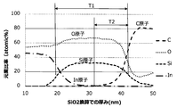
- FIG. 4 shows an example of a profile of X-ray photoelectron spectroscopy. Depth profile measurement for each element of indium In, silicon Si, oxygen O, and carbon C while etching the transparent conductive layer with argon Ar ions from the transparent conductive layer side of the transparent conductive film toward the film substrate The element ratio (atomic%) of the four elements was calculated every 1 nm in terms of silicon dioxide SiO 2 . The existence region in the thickness direction of the impurity atoms (carbon atoms) is expressed by the formula (T 2) according to the thickness T 1 of the silicon dioxide SiO 2 layer measured by the depth profile and the thickness T 2 of the region where the carbon atoms are detected. / T 1 ) X100 (%).
- FIG. 4 is a depth profile of the four elements measured every 1 nm in terms of silicon dioxide (SiO 2 ).
- the horizontal axis indicates the thickness direction (nm), and the vertical axis indicates the element ratio (atomic%).
- the left end is the transparent conductive layer side (surface side), and the right end is the film substrate side.
- the X-ray photoelectron spectroscopy ESCA has a shape with a depth profile due to the nature of the analysis.
- the thickness T 1 of the silicon oxide layer is different from the maximum value of the silicon Si element ratio on the surface side. outermost portion of the film base silicon oxide positions half in side layer, and the deepest portion, and the thickness in between the thickness T 1 of the silicon oxide layer.
- the carbon C atoms calculates the thickness T 2 of the detected region as the impurity atoms, the presence area of the impurity atoms (T 2 / T 1) X100 (%) of Based on this, a region having a carbon atom content of 0.2 atomic% or less was calculated by the formula “100- (T 2 / T 1 ) X100” (%).
- the X-ray diffraction peaks of the transparent conductive layers in the transparent conductive films of Examples and Comparative Examples were obtained by X-ray diffraction measurement using a horizontal X-ray diffractometer SmartLab (manufactured by Rigaku). The measurement was performed under the following conditions, and each peak intensity was a value obtained by subtracting the background. As described above, the X-ray diffraction peak intensities I 222 , I 400 , and I 440 corresponding to the (222) plane, the (400) plane, and the (440) plane are obtained, thereby obtaining I 440 / I 400 and I 400 / I. 222 was obtained.
- the center position (2.5 cm position) on the short side of the sample for scratch resistance evaluation is 10 cm in the long side direction under the following conditions.
- the surface of the transparent conductive layer of the sample for scratch resistance evaluation was rubbed with the length.
- the resistance value (R0) of the sample for scuffing evaluation before rubbing and the resistance value (R20) of the sample for scuffing evaluation after rubbing are set to the central position (5.5 cm) on the long side of the sample for scuffing evaluation.
- Position the scratch resistance was evaluated by applying a tester to the silver paste portions at both ends and determining the resistance change rate (R20 / R0).
Landscapes
- Engineering & Computer Science (AREA)
- General Engineering & Computer Science (AREA)
- Theoretical Computer Science (AREA)
- Human Computer Interaction (AREA)
- Physics & Mathematics (AREA)
- General Physics & Mathematics (AREA)
- Physical Vapour Deposition (AREA)
- Non-Insulated Conductors (AREA)
- Laminated Bodies (AREA)
Abstract
Description
図1は本発明の第1の実施形態に係る透明導電性フィルム10の模式図である。透明導電性フィルム10においては、透明なフィルム基材11と光学調整層12と透明導電層13がこの順に積層されている。光学調整層12は乾式成膜法にて形成された無機酸化物の層(乾式光学調整層)を含む。透明導電層13はインジウムを含んだ金属酸化物を含む。透明導電層13は結晶質であって、少なくとも(400)面、(440)面に対応するX線回折ピークを有する結晶構造を含む。(400)面のX線回折ピーク強度をI400とし、(440)面のX線回折ピーク強度をI440としたとき、X線回折ピーク強度の比I440/I400は1.0~2.2の範囲である。
フィルム基材は、例えば、ポリエチレンテレフタレート、ポリエチレンナフタレート、ポリオレフィン、ポリシクロオレフィン、ポリカーボネート、ポリエーテルスルフォン、ポリアリレート、ポリイミド、ポリアミド、ポリスチレン、ノルボルネンなどの高分子フィルムからなる。フィルム基材の材質はこれらに限定されることはないが、透明性、耐熱性、および機械特性に優れるポリエチレンテレフタレート(PET)が、特に好ましい。
光学調整層は、フィルム基材と透明導電層との間に設けられる屈折率調整のための層である。光学調整層を設けることにより透明導電性フィルムの光学特性(例えば反射特性)を最適化することができる。光学調整層により、透明導電層の配線パターンのある部分と配線パターンのない部分の反射率の差が小さくなるため、透明導電層の配線パターンが視認されにくくなる(透明導電層の配線パターンが視認されることは望ましくない)。
透明導電層は、インジウムを含んだ金属酸化物を含む層、すなわち酸化インジウムを主成分とする透明薄膜層、又はインジウムと1種以上の不純物金属元素を含有する複合金属酸化物を主成分とする透明薄膜層を含む。透明導電層はインジウムを含む層を含み、可視光域で光透過性を有し、かつ、導電性を有するものであれば、その構成材料が特に限定されることはない。また、透明導電層は、好ましくは、インジウムを含んだ金属酸化物からなる。
図2は本発明の第2の実施形態に係る透明導電性フィルム20の模式図である(図1の構成と共通の要素には同じ符号を用いる)。透明導電性フィルム20は、少なくとも、透明なフィルム基材11と、光学調整層12と、第2透明導電性薄膜15と、第1透明導電性薄膜14とがこの順に積層されている。透明導電層は第1透明導電性薄膜14と第2透明導電性薄膜15からなり、第1透明導電性薄膜14および第2透明導電性薄膜15はインジウム以外に1種以上の不純物金属元素を含む。光学調整層12は無機酸化物層を含む乾式光学調整層を含む。
本発明の透明導電性フィルムの具体的な実施形態について、実施例と比較例を対比しながら説明するが、本発明はこれらの実施例に限定されるものではなく、本発明の技術思想に基づいて各種の変形および変更が可能である。
実施例1の透明導電性フィルムは図2に示す層構成である。フィルム基材は厚さ100μmのポリエチレンテレフタレート(PET)フィルムである。光学調整層は、スパッタリングで形成されたケイ素酸化物層からなり、厚さは20nmである。第1透明導電性薄膜は第1インジウムスズ酸化物(ITO)層(厚さ3nm)、第2透明導電性薄膜は第2インジウムスズ酸化物(ITO)層(厚さ19nm)からなる。第1インジウムスズ酸化物層(第1透明導電性薄膜)の、インジウムに対するスズ(不純物金属元素)の含有比(In原子数に対するSn原子数の原子数比Sn/In)は0.03、第2インジウムスズ酸化物層(第2透明導電性薄膜)の、インジウムに対するスズ(不純物金属元素)の含有比(In原子数に対するSn原子数の原子数比Sn/In)は0.10である。
厚さ100μmのポリエチレンテレフタレートフィルム(三菱樹脂製)の主面(光学調整層を形成する側の面)に、アクリル樹脂を含む紫外線硬化性樹脂からなる、厚さ0.3μmのハードコート層を形成し、フィルム基材とした。
光学調整層(及び後に記す第1透明導電性薄膜、第2透明導電性薄膜)はロール・トゥ・ロール型スパッタリング装置を用いて形成された。
光学調整層に引き続き透明導電層を形成した。透明導電層は、第2透明導電性薄膜と第1透明導電性薄膜の2層構造からなる透明導電性薄膜積層体とした。光学調整層が形成されたフィルム基材の背面(光学調整層とは反対側の面)を、表面温度を0℃とした成膜ロールに接触させながら搬送し、光学調整層上に、厚さ19nmの第2透明導電性薄膜(スズ/インジウム含有比Sn/In=0.10)を形成し、続けて第2透明導電性薄膜上に、厚さ3nmの第1透明導電性薄膜(スズ/インジウム含有比Sn/In=0.03)を形成した。
第1インジウムスズ酸化物層(第1透明導電性薄膜)の厚さを6nm、第2インジウムスズ酸化物層(第2透明導電性薄膜)の厚さを16nmとした以外は実施例1と同様にして、実施例2の透明導電性フィルムを作製した。
第1インジウムスズ酸化物層(第1透明導電性薄膜)の厚さを8nm、第2インジウムスズ酸化物層(第2透明導電性薄膜)の厚さを14nmとした以外は実施例1と同様にして、実施例3の透明導電性フィルムを作製した。
第1インジウムスズ酸化物層(第1透明導電性薄膜)の厚さを4nm、第2インジウムスズ酸化物層(第2透明導電性薄膜)の厚さを18nmとした以外は実施例1と同様にして、実施例4の透明導電性フィルムを作製した。
水平磁場100mTのマグネットを用いて、第1インジウムスズ酸化物層(第1透明導電性薄膜)及び第2インジウムスズ酸化物層(第2透明導電性薄膜)を形成したこと以外は、実施例1と同様にして、実施例5の透明導電性フィルムを作製した。水平磁場を30mTから100mTに強くすることにより、透明導電層の比抵抗値が低くなる。
比較例1の透明導電性フィルムの膜構成は図3に示すものである。比較例1は光学調整層が湿式光学調整層である。湿式光学調整層は、メラミン樹脂とアルキド樹脂と有機シラン縮合物の混合物(メラミン樹脂:アルキド樹脂:有機シラン縮合物の重量比は2:2:1)からなる熱硬化樹脂を、有機溶媒に溶解し、フィルム基材に塗工した後、熱硬化させて形成された。湿式光学調整層の厚さは35nmであった。透明導電層は第1インジウムスズ酸化物層および第2インジウムスズ酸化物層の2層からなり、その形成方法は、第1インジウムスズ酸化物層の厚さを4nm、第2インジウムスズ酸化物層の厚さを18nmとした以外は、実施例1と同様にして、比較例1の透明導電性フィルムを作製した。
比較例2の透明導電性フィルムは、インジウムスズ酸化物層が1層であり、膜構成は図1と同じである。アルゴン及び酸素(流量比はアルゴン:酸素=99:1)を導入した0.3Paの真空雰囲気で、8重量%の酸化スズと92重量%の酸化インジウムの焼結体から成るインジウムスズ酸化物ターゲットを、スパッタリングすることで、厚さ21nmのインジウムスズ酸化物層(インジウム/スズ含有比Sn/In=0.08)を作成した。これ以外は実施例1と同様にして、比較例2の透明導電性フィルムを作製した。
比較例3の透明導電性フィルムは、インジウムスズ酸化物層が1層であり、膜構成は図1と同じである。アルゴン及び酸素(流量比はアルゴン:酸素=99:1)を導入した0.3Paの真空雰囲気で、7重量%の酸化スズと93重量%の酸化インジウムの焼結体から成るインジウムスズ酸化物ターゲットをスパッタリングすることで、厚さ22nmのインジウムスズ酸化物層(インジウム/スズ含有比Sn/In=0.07)を作成した。これ以外は実施例1と同様にして、比較例3の透明導電性フィルムを作製した。

実施例1~5および比較例2、3における、光学調整層(スパッタリング法で形成された厚さ20nmのケイ素酸化物層)には、炭素原子が0.2atomic%以下の領域が、厚さ方向に少なくとも50%以上あることをX線光電子分光法(ESCA : Electron Spectroscopy for Chemical Analysis)にて確認した。比較例1における、湿式光学調整層(塗工法で形成された厚さ35nmの熱硬化樹脂層)には、厚さ方向に炭素原子が0.2atomic%以下の領域が無いことをX線光電子分光法にて確認した。
実施例および比較例の透明導電層のエッチング速度は、透明導電層の実質的な導電性が失われる(2端子間抵抗が60MΩを超える)のに要する時間で測定した。本願では、本明細書のエッチング試験条件(後述)において、エッチング時間が110秒以下である場合を「○」とし、110秒を超えた場合を「X」とした。
透明導電層の(222)面のX線回折ピーク強度をI222とし、(400)面のX線回折ピーク強度をI400とし、(440)面のX線回折ピーク強度をI440とする。X線回折ピーク強度の比I400/I222に注目すると、実施例1は0.16、実施例2は0.13、実施例3は0.21、実施例4は0.20、実施例5は0.15であり、いずれも0.10~0.26の範囲内にあった。一方、比較例1は0.06、比較例2は0.09、比較例3は0.27であり、いずれも0.10~0.26の範囲内になかった。
実施例1~5、比較例2、3は光学調整層が乾式光学調整層を含んでいるため、耐擦傷性は問題無かった(〇印)。一方、比較例1は光学調整層が湿式光学調整層のみであるため、耐擦傷性が低かった(X印)。
[膜厚]
フィルム基材の厚さは、膜厚計(尾崎製作所(Peacock(登録商標))社製、装置名「デジタルダイアルゲージ DG-205」)を用いて測定した。また、ハードコート層、光学調整層、透明導電層の厚さは、透過型電子顕微鏡(日立製作所製、装置名「HF-2000」)を用いた断面観察により測定した。
実施例、比較例の透明導電性フィルムの表面抵抗値をJIS K7194に準じて、4端子法を用いて測定した。次いで、測定した表面抵抗値と上記[膜厚]項に記載の方法で求めた透明導電層の厚みとを用いて比抵抗値を算出した。
実施例、比較例の透明導電性フィルムを5cm角の正方形シートに切り出して、温度を50℃に調整した10重量%塩酸に浸漬し、浸漬時間10秒ごとに取り出して水洗浄及び水の拭き取り(乾燥)を行い、任意の3地点における2端子間抵抗をテスターで測定した。なお、2端子間抵抗を測定する際の端子間距離は1.5cmとし、任意の3地点における2端子間抵抗が全て60MΩを超えた時点でエッチングが完了したと判断し、エッチング完了までに要した時間をエッチング時間とした。
光学調整層の炭素原子の厚さ方向の存在領域の評価は、測定装置Quantum2000(アルバック・ファイ社製)を用いて、X線光電子分光法(ESCA)により行った。
各実施例、比較例の透明導電性フィルムにおける透明導電層のX線回折ピークは、水平型X線回折装置SmartLab(Rigaku社製)を用いて、X線回折測定することにより取得した。なお、測定は下記の条件通りに行い、各ピーク強度はバックグラウンドを差し引いた値とした。前記のようにして(222)面、(400)面、(440)面に対応するX線回折ピーク強度I222、I400、I440を求め、それによりI440/I400およびI400/I222を求めた。
・平行ビーム光学配置
・光源:CuKα線(波長:1.54186Å)
・出力:45kV、200mA
・入射側スリット系:ソーラスリット5.0°
・高さ制御スリット:10mm
・入射スリット:0.1mm
・受光側スリット:パラレルスリットアナライザー(PSA)0.114deg.
・検出器:シンチレーションカウンター
・試料ステージ:通常ホルダを用い、ポンプにより試料を吸着固定した。
・X線入射角:0.50°(ただし、十分な強度が得られない場合は、入射角を0.40°、0.45°、0.55°、0.60°でそれぞれ測定し、目的とするピークが最も強くなる結果を採用した。)
・ステップ間隔:0.01°
・測定スピード:3.0°/分
・測定範囲:10°~60°
各実施例、比較例の透明導電性フィルムを5cmX11cmの長方形に切り出し、長辺側の両端部5mm部分に銀ペーストを塗着して、48時間自然乾燥させた。次に、透明導電性フィルムの、透明導電層とは反対の側を、粘着剤付ガラス板に貼付し、擦傷性評価用サンプルを得た。
・擦傷子:アンティコンゴールド(コンテック社製)
・荷重:127g/cm2
・擦傷速度:13cm/秒(7.8m/分)
・擦傷回数:20回(往復10回)
Claims (9)
- 透明なフィルム基材の少なくとも一方の主面に、
少なくとも、光学調整層と、透明導電層とが、この順に積層されてなる透明導電性フィルムであって、
前記光学調整層は、無機酸化物を含む乾式光学調整層を含み、
前記透明導電層は、インジウムを含む金属酸化物を含み、
前記透明導電層は結晶質であって、少なくとも(400)面、(440)面に対応するX線回折ピークを有し、
前記(400)面のX線回折ピーク強度をI400とし、前記(440)面のX線回折ピーク強度をI440としたとき、
前記X線回折ピーク強度の比I440/I400が1.0~2.2の範囲である透明導電性フィルム。 - 透明なフィルム基材の少なくとも一方の主面に、
少なくとも、光学調整層と、透明導電層とが、この順に積層されてなる透明導電性フィルムであって、
前記光学調整層は、無機酸化物を含む乾式光学調整層を含み、
前記透明導電層は、インジウムを含む金属酸化物を含み、
前記透明導電層は結晶質であって、少なくとも(222)面、(400)面、(440)面に対応するX線回折ピークを有し、
前記(222)面のX線回折ピーク強度をI222とし、前記(400)面のX線回折ピーク強度をI400とし、前記(440)面のX線回折ピーク強度をI440としたとき、
前記X線回折ピーク強度の比I400/I222が0.10~0.26の範囲であり、
前記X線回折ピーク強度の比I440/I400が1.0~2.2の範囲である透明導電性フィルム。 - 前記乾式光学調整層は、厚さ方向において、炭素原子の含有量が0.2atomic%以下の無機酸化物の領域を含む、請求項1または2に記載の透明導電性フィルム。
- 前記透明導電層は、2層以上の透明導電性薄膜の積層体からなる透明導電性薄膜積層体であり、
全ての前記透明導電性薄膜は、インジウム以外に1種以上の不純物金属元素を含み、
前記フィルム基材から最も離れた位置にある前記透明導電性薄膜を第1透明導電性薄膜とするとき、
前記第1透明導電性薄膜における、前記インジウムに対する前記不純物金属元素の含有比は、前記透明導電性薄膜積層体を構成する全ての前記透明導電性薄膜における、前記インジウムに対する前記不純物金属元素の含有比の中で最大ではない請求項1乃至3のいずれかに記載の透明導電性フィルム。 - 前記第1透明導電性薄膜における、前記インジウムに対する前記不純物金属元素の含有比が、前記透明導電性薄膜積層体を構成する全ての前記透明導電性薄膜における、前記インジウムに対する前記不純物金属元素の含有比の中で最小である、請求項4に記載の透明導電性フィルム。
- 前記第1透明導電性薄膜は、前記インジウムに対する前記不純物金属元素の含有比が、0.004以上、0.05未満である請求項4または5に記載の透明導電性フィルム。
- 前記透明導電性薄膜積層体を構成する全ての前記透明導電性薄膜の中で、前記第1透明導電性薄膜を除く前記透明導電性薄膜は、前記インジウムに対する前記不純物金属元素の含有比が、0.05以上、0.16以下である請求項4乃至6のいずれかに記載の透明導電性フィルム。
- 前記透明導電性薄膜積層体を構成する複数の前記透明導電性薄膜において、前記第1透明導電性薄膜の膜厚が、前記第1透明導電性薄膜を除く全ての前記透明導電性薄膜の膜厚より小さい請求項4乃至7のいずれかに記載の透明導電性フィルム。
- 前記不純物金属元素がスズ(Sn)からなる、請求項4乃至8のいずれかに記載の透明導電性フィルム。
Priority Applications (3)
| Application Number | Priority Date | Filing Date | Title |
|---|---|---|---|
| CN201580011395.8A CN106062888B (zh) | 2014-12-22 | 2015-11-27 | 透明导电性薄膜 |
| KR1020167014514A KR20170098685A (ko) | 2014-12-22 | 2015-11-27 | 투명 도전성 필름 |
| US15/532,678 US20170358383A1 (en) | 2014-12-22 | 2015-11-27 | Transparent conductive film |
Applications Claiming Priority (4)
| Application Number | Priority Date | Filing Date | Title |
|---|---|---|---|
| JP2014258382 | 2014-12-22 | ||
| JP2014-258382 | 2014-12-22 | ||
| JP2015-223724 | 2015-11-16 | ||
| JP2015223724A JP6661335B2 (ja) | 2014-12-22 | 2015-11-16 | 透明導電性フィルム |
Publications (1)
| Publication Number | Publication Date |
|---|---|
| WO2016104046A1 true WO2016104046A1 (ja) | 2016-06-30 |
Family
ID=56150078
Family Applications (1)
| Application Number | Title | Priority Date | Filing Date |
|---|---|---|---|
| PCT/JP2015/083339 Ceased WO2016104046A1 (ja) | 2014-12-22 | 2015-11-27 | 透明導電性フィルム |
Country Status (1)
| Country | Link |
|---|---|
| WO (1) | WO2016104046A1 (ja) |
Cited By (1)
| Publication number | Priority date | Publication date | Assignee | Title |
|---|---|---|---|---|
| CN114127864A (zh) * | 2019-08-06 | 2022-03-01 | 日东电工株式会社 | 透明导电性薄膜 |
Citations (6)
| Publication number | Priority date | Publication date | Assignee | Title |
|---|---|---|---|---|
| JP2000128698A (ja) * | 1998-10-22 | 2000-05-09 | Toyota Motor Corp | Ito材、ito膜及びその形成方法、並びにel素子 |
| WO2000051139A1 (en) * | 1999-02-24 | 2000-08-31 | Teijin Limited | Transparent conductive laminate, its manufacturing method, and display comprising transparent conductive laminate |
| JP2007141755A (ja) * | 2005-11-22 | 2007-06-07 | Dainippon Printing Co Ltd | 導電性基板 |
| WO2013014134A2 (en) * | 2011-07-22 | 2013-01-31 | Universitätsklinikum Hamburg-Eppendorf | Polyoma virus jc peptides and proteins in vaccination and diagnostic applications |
| JP2014096222A (ja) * | 2012-11-07 | 2014-05-22 | Nitto Denko Corp | 透明導電性フィルム |
| JP2015146253A (ja) * | 2014-02-03 | 2015-08-13 | 大日本印刷株式会社 | 積層体およびタッチパネル用導電性パターン基材 |
-
2015
- 2015-11-27 WO PCT/JP2015/083339 patent/WO2016104046A1/ja not_active Ceased
Patent Citations (6)
| Publication number | Priority date | Publication date | Assignee | Title |
|---|---|---|---|---|
| JP2000128698A (ja) * | 1998-10-22 | 2000-05-09 | Toyota Motor Corp | Ito材、ito膜及びその形成方法、並びにel素子 |
| WO2000051139A1 (en) * | 1999-02-24 | 2000-08-31 | Teijin Limited | Transparent conductive laminate, its manufacturing method, and display comprising transparent conductive laminate |
| JP2007141755A (ja) * | 2005-11-22 | 2007-06-07 | Dainippon Printing Co Ltd | 導電性基板 |
| WO2013014134A2 (en) * | 2011-07-22 | 2013-01-31 | Universitätsklinikum Hamburg-Eppendorf | Polyoma virus jc peptides and proteins in vaccination and diagnostic applications |
| JP2014096222A (ja) * | 2012-11-07 | 2014-05-22 | Nitto Denko Corp | 透明導電性フィルム |
| JP2015146253A (ja) * | 2014-02-03 | 2015-08-13 | 大日本印刷株式会社 | 積層体およびタッチパネル用導電性パターン基材 |
Cited By (1)
| Publication number | Priority date | Publication date | Assignee | Title |
|---|---|---|---|---|
| CN114127864A (zh) * | 2019-08-06 | 2022-03-01 | 日东电工株式会社 | 透明导电性薄膜 |
Similar Documents
| Publication | Publication Date | Title |
|---|---|---|
| JP6661335B2 (ja) | 透明導電性フィルム | |
| JP5932098B2 (ja) | 透明導電性フィルム | |
| JP5932097B2 (ja) | 透明導電性フィルム | |
| JP6548910B2 (ja) | 電界駆動型調光素子用透明導電性フィルム、調光フィルム、および電界駆動型調光素子 | |
| JP5957133B2 (ja) | 保護フィルム付き透明導電性フィルム | |
| CN105874544B (zh) | 透明导电膜及其制造方法 | |
| CN115298764A (zh) | 透明导电性薄膜和透明导电性薄膜的制造方法 | |
| JP2014164882A (ja) | 信頼性・加工性に優れた積層体およびフィルムセンサ並びに積層体製造方法 | |
| WO2015166963A1 (ja) | 透明導電性フィルム及びその製造方法 | |
| JP6144798B2 (ja) | 透明導電性フィルム | |
| Kim et al. | Flexible and transparent TiO2/Ag/ITO multilayer electrodes on PET substrates for organic photonic devices | |
| WO2016104046A1 (ja) | 透明導電性フィルム | |
| CN106460153A (zh) | 透明导电性膜及其制造方法 | |
| JP6161763B2 (ja) | 透明導電性フィルム | |
| Park et al. | Properties of IZTO Thin Films Deposited on PET Substrates with The SiO 2 Buffer Layer | |
| WO2016189762A1 (ja) | 透明導電性フィルム | |
| WO2016080246A1 (ja) | 保護フィルム付き透明導電性フィルム | |
| JP2005183007A (ja) | 透明導電性シート | |
| TW202436262A (zh) | 具有光吸收器的太陽能控制玻璃 | |
| WO2015159804A1 (ja) | 積層体、導電性積層体、および電子機器 |
Legal Events
| Date | Code | Title | Description |
|---|---|---|---|
| ENP | Entry into the national phase |
Ref document number: 20167014514 Country of ref document: KR Kind code of ref document: A |
|
| 121 | Ep: the epo has been informed by wipo that ep was designated in this application |
Ref document number: 15872615 Country of ref document: EP Kind code of ref document: A1 |
|
| WWE | Wipo information: entry into national phase |
Ref document number: 15532678 Country of ref document: US |
|
| NENP | Non-entry into the national phase |
Ref country code: DE |
|
| 122 | Ep: pct application non-entry in european phase |
Ref document number: 15872615 Country of ref document: EP Kind code of ref document: A1 |