WO2016092964A1 - 電子デバイスパッケージ、及び、封止用シート - Google Patents
電子デバイスパッケージ、及び、封止用シート Download PDFInfo
- Publication number
- WO2016092964A1 WO2016092964A1 PCT/JP2015/080420 JP2015080420W WO2016092964A1 WO 2016092964 A1 WO2016092964 A1 WO 2016092964A1 JP 2015080420 W JP2015080420 W JP 2015080420W WO 2016092964 A1 WO2016092964 A1 WO 2016092964A1
- Authority
- WO
- WIPO (PCT)
- Prior art keywords
- sealing
- electronic device
- device package
- sealing sheet
- semiconductor chip
- Prior art date
- Legal status (The legal status is an assumption and is not a legal conclusion. Google has not performed a legal analysis and makes no representation as to the accuracy of the status listed.)
- Ceased
Links
Images






Classifications
-
- H—ELECTRICITY
- H03—ELECTRONIC CIRCUITRY
- H03H—IMPEDANCE NETWORKS, e.g. RESONANT CIRCUITS; RESONATORS
- H03H9/00—Networks comprising electromechanical or electro-acoustic elements; Electromechanical resonators
- H03H9/25—Constructional features of resonators using surface acoustic waves
-
- H—ELECTRICITY
- H10—SEMICONDUCTOR DEVICES; ELECTRIC SOLID-STATE DEVICES NOT OTHERWISE PROVIDED FOR
- H10W—GENERIC PACKAGES, INTERCONNECTIONS, CONNECTORS OR OTHER CONSTRUCTIONAL DETAILS OF DEVICES COVERED BY CLASS H10
- H10W74/00—Encapsulations, e.g. protective coatings
-
- H—ELECTRICITY
- H10—SEMICONDUCTOR DEVICES; ELECTRIC SOLID-STATE DEVICES NOT OTHERWISE PROVIDED FOR
- H10W—GENERIC PACKAGES, INTERCONNECTIONS, CONNECTORS OR OTHER CONSTRUCTIONAL DETAILS OF DEVICES COVERED BY CLASS H10
- H10W76/00—Containers; Fillings or auxiliary members therefor; Seals
- H10W76/10—Containers or parts thereof
- H10W76/12—Containers or parts thereof characterised by their shape
-
- H—ELECTRICITY
- H10—SEMICONDUCTOR DEVICES; ELECTRIC SOLID-STATE DEVICES NOT OTHERWISE PROVIDED FOR
- H10W—GENERIC PACKAGES, INTERCONNECTIONS, CONNECTORS OR OTHER CONSTRUCTIONAL DETAILS OF DEVICES COVERED BY CLASS H10
- H10W90/00—Package configurations
- H10W90/701—Package configurations characterised by the relative positions of pads or connectors relative to package parts
- H10W90/721—Package configurations characterised by the relative positions of pads or connectors relative to package parts of bump connectors
- H10W90/724—Package configurations characterised by the relative positions of pads or connectors relative to package parts of bump connectors between a chip and a stacked insulating package substrate, interposer or RDL
Definitions
- the present invention relates to an electronic device package and a sealing sheet.
- semiconductor chips in which functional elements having movable parts such as MEMS (Micro Electro Mechanical Systems) and SAW (Surface Acoustic Wave) filters are formed on the bump forming surface.
- a semiconductor chip cannot cover the movable part with a sealing resin or the like.
- the semiconductor chip is flip-chip connected to the mounting substrate so that the movable portion faces the mounting substrate, and a hollow structure is formed between the movable portion of the semiconductor chip and the mounting substrate.
- a hollow electronic device package can be manufactured using the sheet-shaped sealing resin as described above.
- This invention is made
- Another object of the present invention is to provide a sealing sheet that can be used to manufacture the electronic device package.
- the present invention is an electronic device package, A sealed body; A sealing layer for sealing the object to be sealed;
- the sealed object has a non-contact portion that is not in contact with the sealing layer on at least a part of the upper surface and the side surface of the sealed object.
- the sealed body has a new shape having a non-contact portion that is not in contact with the sealing layer on at least a part of the top surface and the side surface of the sealed body.
- An electronic device package can be provided.
- the electronic device package may have a sealing layer formed so as to surround a part or the whole of the object to be sealed, and a part of the object to be sealed may be exposed.
- a part or the whole of the object to be sealed may be surrounded by the sealing layer, and the object to be sealed and the sealing layer may or may not be in contact.
- a functional element having a movable portion is formed on the top surface of the sealed body,
- the sealed body preferably has a non-contact portion that is not in contact with the sealing layer at least in a portion where the functional element is formed.
- the movable portion of the functional element is not brought into contact with the sealing layer. That is, according to the said structure, it can be set as the electronic device package of the form by which the functional element which has a movable part is formed in the upper surface of the to-be-sealed body.
- a photoelectric conversion element is formed on the top surface of the object to be sealed. It is also preferable that the sealed body has a non-contact portion that is not in contact with the sealing layer at least in a portion where the photoelectric conversion element is formed.
- the photoelectric conversion element when the photoelectric conversion element is formed on the upper surface of the object to be sealed, the photoelectric conversion element is not brought into contact with the sealing layer. That is, according to the said structure, it can be set as the electronic device package of the form by which the photoelectric conversion element is formed in the upper surface of a to-be-sealed body.
- the sealing layer is preferably formed using a sheet-like sealing sheet.
- the “sheet-like sealing sheet” refers to a sealing sheet having a sheet form, and includes a sheet in which a recess or a hole is formed.
- the sealing layer is formed using a liquid sealing resin, it is difficult to seal the sealed body without contacting the top surface and side surfaces of the sealed body. Moreover, if the sealing layer is formed by compression molding using a pellet-shaped resin, sealing the sealed body without contacting the top surface and the side surface of the sealed body Have difficulty. On the other hand, according to the said structure, since the said sealing layer is formed using the sheet-like sealing sheet, if a recessed part and a through-hole are provided in a sheet-like sealing sheet, for example The electronic device package is easy to manufacture.
- sealing sheet according to the present invention is characterized in that a plurality of recesses or through holes are formed.
- the sealing sheet according to the present invention has a plurality of recesses or through holes. Therefore, for example, when a plurality of objects to be sealed are collectively sealed, the plurality of objects to be sealed are sealed on the objects to be sealed so that the positions of the plurality of recesses or the through holes correspond to each other. If a flat plate press etc. are carried out after arrange
- an electronic device package having a portion whose upper surface or side surface is not in contact with the sealing layer can be provided.
- seat for sealing which can be utilized in manufacturing the said electronic device package can be provided.
- FIG. 1 is a front sectional view of the electronic device package according to the first embodiment.
- an electronic device package 10 according to the first embodiment includes a mounting substrate 14, a semiconductor chip 16 flip-chip connected to the mounting substrate 14 (corresponding to a sealed body of the present invention), And a sealing layer 12 for sealing the semiconductor chip 16.
- the sealing layer 12 is formed on the mounting substrate 14 so as not to contact either the upper surface 16a or the side surface 16b of the semiconductor chip 16. That is, in the electronic device package 10, the semiconductor chip 16 has the non-contact portion 19 that is not in contact with the sealing layer 12 on the entire upper surface 16 a and side surface 16 b of the semiconductor chip 16.
- Bumps 18 for flip chip connection are formed on a surface 16c (hereinafter also referred to as a bump formation surface 16c) opposite to the upper surface 16a of the semiconductor chip 16, and the bumps 18 are provided on the mounting substrate 14 via the bumps 18. It is connected.
- a functional element having a movable part is formed on the upper surface 16a (not shown).
- MEMS Micro * Electro
- SAW Surface * Acoustic * Wave
- a SAW filter and a pressure sensor are particularly preferable because they are completely sealed and cannot be directly contacted from the outside.
- the gap 17 between the bump forming surface 16c of the semiconductor chip 16 and the mounting substrate 14 may or may not be sealed (underfilled) with resin depending on the application.
- Examples of the mounting substrate 14 include a printed wiring board and a semiconductor wafer on which a circuit is formed.
- the semiconductor chip 16 has a new shape of the electronic device package 10 having the non-contact portion 19 that is not in contact with the sealing layer 12 on the entire upper surface 16 a and side surface 16 b of the semiconductor chip 16. Can be provided.
- the functional element is formed on the upper surface 16 a of the semiconductor chip 16, and the movable part of the functional element is not brought into contact with the sealing layer 12. That is, according to the above configuration, an electronic device package in which a functional element having a movable portion is formed on the upper surface 16a of the semiconductor chip 16 can be obtained.
- FIG. 2 is a front sectional view of the electronic device package according to the second embodiment.
- an electronic device package 30 according to the second embodiment includes a mounting substrate 34, a semiconductor chip 36 flip-chip connected to the mounting substrate 34 (corresponding to the object to be sealed of the present invention), And a sealing layer 32 for sealing the semiconductor chip 36.
- the sealing layer 32 is formed on the mounting substrate 34 in such a manner that it does not contact with part of the upper surface 36a and part of the side surface 36b of the semiconductor chip 36 and does not contact with other parts. That is, the electronic device package 30 has the non-contact portion 39 in which the semiconductor chip 36 is not in contact with the sealing layer 32 in a part of the upper surface 36 a and a part of the side surface 36 b of the semiconductor chip 36.
- Bumps 38 for flip-chip connection are formed on a surface 36c (hereinafter also referred to as a bump formation surface 36c) opposite to the upper surface 36a of the semiconductor chip 36, and is mounted on the mounting substrate 34 via the bumps 38. It is connected.
- a functional element having a movable part is formed on the upper surface 36a (not shown).
- the sealing layer 32 is not formed on the place where the functional element having the movable part is formed.
- the functional element having the movable portion is not particularly limited, and examples thereof include a MEMS (Micro Electro Mechanical Systems), a SAW (Surface Acoustic Wave) filter, and the like.
- a pressure sensor and a gyro sensor are particularly preferable in that various inputs from the outside can be directly performed without going through the sealing layer 12.
- the gap 37 between the bump forming surface 16c of the semiconductor chip 36 and the mounting substrate 34 may or may not be sealed (underfilled) with resin depending on the application.
- the semiconductor chip 16 is exposed to the outside, it is preferable that the semiconductor chip 16 is underfilled.
- Examples of the mounting substrate 34 include a printed wiring board, a semiconductor wafer on which a circuit is formed, and the like.
- the electronic device package 30 functional elements are formed on a part of the upper surface 36a of the semiconductor chip 36. Then, a part of the upper surface 36 a and a part of the side surface 36 b of the semiconductor chip 36 including the part where the functional element is formed are not brought into contact with the sealing layer 32. That is, according to the above configuration, an electronic device package in which a functional element having a movable portion is formed on the upper surface 36a of the semiconductor chip 36 can be obtained.
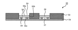
- FIG. 3 is a front sectional view of the electronic device package according to the third embodiment.
- an electronic device package 50 according to the third embodiment includes a mounting substrate 54, a semiconductor chip 56 flip-chip connected to the mounting substrate 54 (corresponding to the object to be sealed of the present invention), And a sealing layer 52 that seals the semiconductor chip 56.
- the sealing layer 52 is formed on the mounting substrate 54 so as to be in contact with the entire side surface 56b of the semiconductor chip 56 and not in contact with the upper surface 56a. That is, the electronic device package 50 has a non-contact portion 59 that is not in contact with the sealing layer 52 over the entire upper surface 56 a of the semiconductor chip 56.
- Bumps 58 for flip-chip connection are formed on a surface 56c (hereinafter also referred to as a bump formation surface 56c) opposite to the upper surface 56a of the semiconductor chip 56, and is mounted on the mounting substrate 54 via the bumps 58. It is connected.
- a photoelectric conversion element is formed on the upper surface 56a (not shown).
- the photoelectric conversion element may be a device that converts light incident on the surface 56a from the outside into electric energy, and converts the electric energy supplied from the bump 58 or the like into light and emits it from the surface 56a to the outside. It may be a thing.
- the gap 57 between the bump forming surface 56c of the semiconductor chip 56 and the mounting substrate 54 may or may not be sealed (underfilled) with resin.
- a photoelectric conversion element is formed on the entire upper surface 56a of the semiconductor chip 56 in order to increase the light emission efficiency or the light reception efficiency. Therefore, the entire upper surface 56a of the semiconductor chip 56 is not covered by the sealing layer.
- Examples of the mounting substrate 54 include a printed wiring board, a semiconductor wafer on which a circuit is formed, and the like.
- the entire upper surface 56a of the semiconductor chip 56 of the semiconductor chip 56 has the non-contact portion 59 that is not in contact with the sealing layer 52. That is, according to the above configuration, an electronic device package in which a photoelectric conversion element is formed on the upper surface 56a of the semiconductor chip 56 can be obtained.
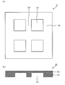
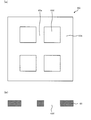
- FIG. 4A is a bottom view of the sealing sheet 20 used for manufacturing the electronic device package 10
- FIG. 4B is a front sectional view thereof.
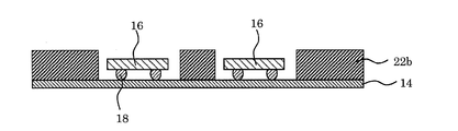
- FIG. 5A is a front sectional view of a stacked body 25 in which a plurality of semiconductor chips 16 are mounted on a mounting substrate 14.
- a sealing sheet 20 having a recess 22c is prepared (step A).
- the sealing sheet 20 includes a flat plate-like portion 22a and a lattice-like lattice portion 22b formed on the plate-like portion 22a. A portion on the plate-like portion 22a where the lattice-like portion 22b is not formed corresponds to the concave portion 22c.
- the recess 22c is formed according to the arrangement of the plurality of semiconductor chips 16 to be sealed.
- a case where four recesses 22c are formed will be described.
- the present invention is not limited to this example, and the number of recesses is not particularly limited.
- this embodiment demonstrates the case where the shape of all the four recessed parts 22c is the same, in this invention, it is not limited to this example, You may differ.
- it is good also as sealing the to-be-sealed body from which a magnitude
- the constituent material of the sealing sheet 20 includes an epoxy resin and a phenol resin as a curing agent. Thereby, favorable thermosetting is obtained.
- the epoxy resin is not particularly limited.
- triphenylmethane type epoxy resin, cresol novolac type epoxy resin, biphenyl type epoxy resin, modified bisphenol A type epoxy resin, bisphenol A type epoxy resin, bisphenol F type epoxy resin, modified bisphenol F type epoxy resin, dicyclopentadiene type Various epoxy resins such as an epoxy resin, a phenol novolac type epoxy resin, and a phenoxy resin can be used. These epoxy resins may be used alone or in combination of two or more.
- the epoxy equivalent is 150 to 250 and the softening point or the melting point is 50 to 130 ° C., solid at room temperature. From the viewpoint, triphenylmethane type epoxy resin, cresol novolac type epoxy resin, and biphenyl type epoxy resin are more preferable.
- the phenol resin is not particularly limited as long as it causes a curing reaction with the epoxy resin.
- a phenol novolac resin, a phenol aralkyl resin, a biphenyl aralkyl resin, a dicyclopentadiene type phenol resin, a cresol novolak resin, a resole resin, or the like is used.
- These phenolic resins may be used alone or in combination of two or more.
- phenol resin those having a hydroxyl equivalent weight of 70 to 250 and a softening point of 50 to 110 ° C. are preferably used from the viewpoint of reactivity with the epoxy resin, and phenol phenol is particularly preferable from the viewpoint of high curing reactivity.
- a novolac resin can be suitably used. From the viewpoint of reliability, low hygroscopic materials such as phenol aralkyl resins and biphenyl aralkyl resins can also be suitably used.
- the blending ratio of the epoxy resin and the phenol resin is blended so that the total of hydroxyl groups in the phenol resin is 0.7 to 1.5 equivalents with respect to 1 equivalent of the epoxy group in the epoxy resin from the viewpoint of curing reactivity. It is preferable to use 0.9 to 1.2 equivalents.
- the total content of the epoxy resin and the phenol resin in the sealing sheet 20 is preferably 2.5% by weight or more, and more preferably 3.0% by weight or more. Adhesive strength with respect to the semiconductor chip 16 can be obtained satisfactorily when it is 2.5% by weight or more.
- the total content of the epoxy resin and the phenol resin in the sealing sheet 20 is preferably 20% by weight or less, and more preferably 10% by weight or less. Hygroscopicity can be reduced as it is 20 weight% or less.
- the sealing sheet 20 preferably contains a thermoplastic resin. Thereby, the handleability at the time of non-hardening and the low stress property of hardened
- thermoplastic resin examples include natural rubber, butyl rubber, isoprene rubber, chloroprene rubber, ethylene-vinyl acetate copolymer, ethylene-acrylic acid copolymer, ethylene-acrylic acid ester copolymer, polybutadiene resin, polycarbonate resin, heat Plastic polyimide resin, polyamide resin such as 6-nylon and 6,6-nylon, phenoxy resin, acrylic resin, saturated polyester resin such as PET and PBT, polyamideimide resin, fluororesin, styrene-isobutylene-styrene block copolymer, etc. Is mentioned. These thermoplastic resins can be used alone or in combination of two or more. Of these, a styrene-isobutylene-styrene block copolymer is preferable from the viewpoint of low stress and low water absorption.
- the content of the thermoplastic resin in the sealing sheet 20 is preferably 1.5% by weight or more, and more preferably 2.0% by weight or more. A softness
- the content of the thermoplastic resin in the sealing sheet 20 is preferably 6% by weight or less, and more preferably 4% by weight or less. Adhesiveness with the semiconductor chip 16 is favorable as it is 4 weight% or less.
- the sealing sheet 20 preferably contains an inorganic filler.
- the inorganic filler is not particularly limited, and various conventionally known fillers can be used.
- quartz glass, talc, silica such as fused silica and crystalline silica
- alumina aluminum nitride
- nitriding Examples thereof include silicon and boron nitride powders. These may be used alone or in combination of two or more. Among these, silica and alumina are preferable, and silica is more preferable because the linear expansion coefficient can be satisfactorily reduced.
- silica powder is preferable, and fused silica powder is more preferable.
- fused silica powder examples include spherical fused silica powder and crushed fused silica powder. From the viewpoint of fluidity, spherical fused silica powder is preferable. Among these, those having an average particle diameter in the range of 10 to 30 ⁇ m are preferable, and those having a mean particle diameter in the range of 15 to 25 ⁇ m are more preferable.
- the average particle diameter can be derived, for example, by using a sample arbitrarily extracted from the population and measuring it using a laser diffraction / scattering particle size distribution measuring apparatus.
- the content of the inorganic filler in the sealing sheet 20 is preferably 75 to 95% by weight, more preferably 78 to 95% by weight with respect to the entire sealing sheet 20.
- the content of the inorganic filler is 75% by weight or more with respect to the entire sealing sheet 20, the mechanical expansion due to thermal shock can be suppressed by suppressing the thermal expansion coefficient low.
- the content of the inorganic filler is 95% by weight or less with respect to the entire sealing sheet 20, flexibility, fluidity, and adhesiveness are improved.
- the sealing sheet 20 includes a curing accelerator.
- the curing accelerator is not particularly limited as long as it can cure the epoxy resin and the phenol resin, and examples thereof include organophosphorus compounds such as triphenylphosphine and tetraphenylphosphonium tetraphenylborate; 2-phenyl-4, And imidazole compounds such as 5-dihydroxymethylimidazole and 2-phenyl-4-methyl-5-hydroxymethylimidazole.
- organophosphorus compounds such as triphenylphosphine and tetraphenylphosphonium tetraphenylborate
- 2-phenyl-4, And imidazole compounds such as 5-dihydroxymethylimidazole and 2-phenyl-4-methyl-5-hydroxymethylimidazole.
- 2-phenyl-4,5-dihydroxymethylimidazole is preferable because the curing reaction does not rapidly proceed even when the temperature rises during kneading and the sealing sheet 20 can be satisfactorily produced.
- the content of the curing accelerator is preferably 0.1 to 5 parts by weight with respect to 100 parts by weight of the total of the epoxy resin and the phenol resin.
- the sealing sheet 20 contains a flame retardant component. This can reduce the expansion of combustion when ignition occurs due to component short-circuiting or heat generation.
- a flame retardant composition for example, various metal hydroxides such as aluminum hydroxide, magnesium hydroxide, iron hydroxide, calcium hydroxide, tin hydroxide, complex metal hydroxides; phosphazene flame retardants, etc. should be used. Can do.
- the content of the phosphorus element contained in the phosphazene flame retardant is preferably 12% by weight or more.
- the content of the flame retardant component in the sealing sheet 20 is preferably 10% by weight or more, and more preferably 15% by weight or more in the total organic components (excluding inorganic fillers). A flame retardance is favorably acquired as it is 10 weight% or more.
- the content of the thermoplastic resin in the sealing sheet 20 is preferably 30% by weight or less, and more preferably 25% by weight or less. When the content is 30% by weight or less, there is a tendency that there is little decrease in physical properties of the cured product (specifically, physical properties such as glass transition temperature and high-temperature resin strength).
- the sealing sheet 20 preferably contains a silane coupling agent.
- the silane coupling agent is not particularly limited, and examples thereof include 3-glycidoxypropyltrimethoxysilane.
- the content of the silane coupling agent in the sealing sheet 20 is preferably 0.1 to 3% by weight. When the content is 0.1% by weight or more, sufficient strength of the cured product can be obtained and the water absorption rate can be lowered. If it is 3% by weight or less, the outgas amount can be lowered.
- the sealing sheet 20 is preferably colored. Thereby, excellent marking properties and appearance can be exhibited, and a semiconductor device having an added-value appearance can be obtained. Since the colored sealing sheet 20 has excellent marking properties, it can be marked to give various information such as character information and graphic information.
- a coloring material (coloring agent) can be used according to the target color.
- a color material various dark color materials such as a black color material, a blue color material, and a red color material can be suitably used, and a black color material is particularly suitable.
- the color material any of a pigment, a dye and the like may be used. Color materials can be used alone or in combination of two or more.
- the dye any form of dyes such as acid dyes, reactive dyes, direct dyes, disperse dyes, and cationic dyes can be used.
- the form of the pigment is not particularly limited, and can be appropriately selected from known pigments.
- the thickness of the sealing sheet 20 is not particularly limited, but at least from the viewpoint of embedding the semiconductor chip 16, it is the same as or thicker than the semiconductor chip 16 Those are preferred. Specifically, from the viewpoint of use as a sealing sheet, the thickness is, for example, 50 ⁇ m to 2000 ⁇ m.
- the depth of the recess 22c is preferably deeper than the thickness of the semiconductor chip 16 from the viewpoint of not touching the upper surface 16a of the semiconductor chip 16 during sealing.
- the entire sealing sheet 20 may become thin during sealing.
- the depth is preferably 1.05 to 1.40 times the thickness of the semiconductor chip. Specifically, for example, the thickness is 10 ⁇ m to 80 ⁇ m.
- the manufacturing method of the sealing sheet 20 is not particularly limited, the plate-like portion 22a and the lattice-like portion are formed using a mold or the like having a shape corresponding to the sealing sheet 20 after forming a flat resin sheet. 22b and a method of batch forming into a shape in which the recess 22c is formed. Moreover, the method of putting a pellet-shaped resin material in the cavity of the metal mold
- the manufacturing method of said flat resin sheet for manufacturing the sealing sheet 20 is not specifically limited, the kneaded material of the resin composition for forming the sealing sheet 20 was prepared, and the obtained kneading
- a kneaded product is prepared by melt-kneading each component described below with a known kneader such as a mixing roll, a pressure kneader, or an extruder, and the obtained kneaded product is coated or plastically processed into a sheet. Shape.
- the temperature is preferably equal to or higher than the softening point of each component described above, for example, 30 to 150 ° C., and preferably 40 to 140 ° C., more preferably 60 to 120 in consideration of the thermosetting property of the epoxy resin. ° C.
- the time is, for example, 1 to 30 minutes, preferably 5 to 15 minutes.
- the kneading is preferably performed under reduced pressure conditions (under reduced pressure atmosphere). Thereby, while being able to deaerate, the penetration
- the pressure under reduced pressure is preferably 0.1 kg / cm 2 or less, more preferably 0.05 kg / cm 2 or less.
- the lower limit of the pressure under reduced pressure is not particularly limited, but is, for example, 1 ⁇ 10 ⁇ 4 kg / cm 2 or more.
- the kneaded material after melt-kneading is preferably applied in a high temperature state without cooling.
- the coating method is not particularly limited, and examples thereof include a bar coating method, a knife coating method, and a slot die method.
- the temperature at the time of coating is preferably not less than the softening point of each component described above, and considering the thermosetting property and moldability of the epoxy resin, for example, 40 to 150 ° C., preferably 50 to 140 ° C., more preferably 70 to 120 ° C.
- the kneaded product after melt-kneading is preferably subjected to plastic processing in a high temperature state without cooling.
- the plastic working method is not particularly limited, and examples thereof include a flat plate pressing method, a T-die extrusion method, a screw die extrusion method, a roll rolling method, a roll kneading method, an inflation extrusion method, a coextrusion method, and a calendar molding method.
- the plastic working temperature is preferably not less than the softening point of each component described above, and is 40 to 150 ° C., preferably 50 to 140 ° C., more preferably 70 to 120 ° C. in consideration of the thermosetting property and moldability of the epoxy resin. is there.
- the kneaded material may be plastically processed to directly form the shape of the sealing sheet 20.
- the flat resin sheet may be obtained by dissolving and dispersing a resin or the like for forming the sealing sheet 20 in an appropriate solvent to adjust the varnish and coating the varnish.
- substrate 14 is prepared (process B).
- a known device such as a flip chip bonder or a die bonder can be used for mounting the semiconductor chip 16 on the mounting substrate 14.
- the semiconductor chip 16 and the mounting substrate 14 are electrically connected via bumps 18.
- the sealing sheet 20 is disposed on the stacked body 25 so that the semiconductor chip 16 is disposed in the recess 22 c (step C). At this time, the sealing sheet 20 is disposed so as not to touch the upper surface 16 a and the side surface 16 b of the semiconductor chip 16.
- sealing body forming process Next, for example, the sealing sheet 20 is fixed to the mounting substrate 14 by hot pressing with a lower heating plate and an upper heating plate (not shown). Thereby, the sealing body 28 is formed (process D).
- the temperature is, for example, 40 to 150 ° C., preferably 60 to 120 ° C.
- the pressure is, for example, 0.1 to 10 MPa, preferably 0.5 to 8 MPa.
- the decompression condition is, for example, 0.1 to 5 kPa, more preferably 0.1 to 100 Pa.
- the sealing sheet 20 is thermally cured to form the sealing layer 12 (step E). Specifically, for example, the entire sealing body 28 is heated. Thus, the electronic device package 10 (see FIG. 1) is obtained.
- the heating temperature is preferably 100 ° C or higher, more preferably 120 ° C or higher.
- the upper limit of the heating temperature is preferably 200 ° C. or lower, more preferably 180 ° C. or lower.
- the heating time is preferably 10 minutes or more, more preferably 30 minutes or more.
- the upper limit of the heating time is preferably 180 minutes or less, more preferably 120 minutes or less.
- you may pressurize as needed Preferably it is 0.1 Mpa or more, More preferably, it is 0.5 Mpa or more.
- the upper limit is preferably 10 MPa or less, more preferably 5 MPa or less.
- the electronic device package 10 may be diced for each unit of the semiconductor chip 16 as necessary. Thereby, an electronic device package in which one semiconductor chip 16 is sealed can be obtained.
- the sealing sheet may be prepared by separately preparing the plate-like portion 22a and the lattice-like portion 22b, and pressing them to form the sealing sheet 20. This example will be described below.
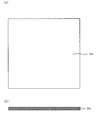
- FIG. 7A is a bottom view of the plate-like portion 22a used for manufacturing the sealing sheet 20, and FIG. 7B is a front sectional view thereof.
- FIG. 8A is a bottom view of the lattice portion 22b used for manufacturing the sealing sheet 20, and FIG. 8B is a front sectional view thereof.
- FIG. 9 is a front cross-sectional view of the plate-like portion 22a and the lattice-like portion 22b, and shows a state in which both are crimped.
- the plate-like portion 22a is created (see FIGS. 7A and 7B). Moreover, the lattice-like part 22b is created (refer to FIG. 8A and FIG. 8B).
- a kneaded product of a resin composition for forming the sealing sheet 20 is prepared, and the obtained kneaded product is applied, or the obtained kneaded product is formed into a sheet.
- the method of plastic working is preferred.
- a resin or the like for forming the sealing sheet 20 can be dissolved and dispersed in an appropriate solvent to adjust the varnish, and the varnish can be applied.
- the lattice-like portion 22b As a method for creating the lattice-like portion 22b, it can be obtained by forming a flat resin sheet using the resin composition for forming the sealing sheet 20, and then punching out the portion that becomes the recess 22c. .
- the plate-like portion 22a and the lattice-like portion 22b are pressure-bonded. Thereby, the sealing sheet 20 can be obtained. In the above, the other manufacturing method of the sealing sheet 20 was demonstrated.
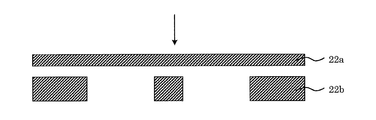
- FIGS. 10 and 11 are front sectional views for explaining another method for manufacturing the electronic device package 10 according to the first embodiment.
- a stacked body 25 (see FIG. 5) in which a plurality of semiconductor chips 16 are mounted on the mounting substrate 14 is prepared.
- a separately formed grid portion 22b (see FIG. 8) is placed on the laminate 25 (FIG. 10). At this time, the grid portion 22b is placed on the mounting substrate 14 so that the grid portion 22b does not touch the semiconductor chip 16.
- a plate-like portion 22a created separately is arranged on the lattice-like portion 22b (see FIG. 11).
- the grid-like portion 22b and the plate-like portion 22a are fixed to the mounting substrate 14 by hot pressing with a lower heating plate and an upper heating plate (not shown). Thereafter, the lattice-like portion 22b and the plate-like portion 22a are thermally cured to form the sealing layer 12.
- the electronic device package 10 (see FIG. 1) is also obtained by the above.
- FIG. 12A is a bottom view of the sealing sheet 40 used for manufacturing the electronic device package 30, and FIG. 12B is a front sectional view thereof.
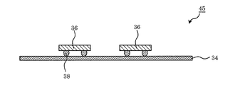
- FIG. 13 is a front sectional view of a stacked body 45 in which a plurality of semiconductor chips 36 are mounted on a mounting substrate 34.
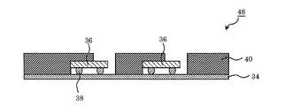
- FIG. 14 is a front sectional view showing a state in which the sealing sheet 40 is disposed on the laminated body 45.
- the sealing sheet 40 includes a plate-like plate-like portion 42a partially having a through-hole 42d, and a lattice-like lattice-like portion 42b formed on the plate-like portion 42a. A portion on the plate-like portion 22a where the lattice-like portion 22b is not formed corresponds to the concave portion 42c.
- the recess 42c is formed according to the arrangement of the plurality of semiconductor chips 36 to be sealed. In the present embodiment, a case where a part of the plate-like portion 42a is in contact with the upper surface of the semiconductor chip 36 will be described. However, in the present invention, it may not be in contact.
- the constituent material of the sealing sheet 40 can be the same as that of the sealing sheet 20.
- the manufacturing method of the sealing sheet 40 can be the same as that of the sealing sheet 20.
- it may be integrally formed from a resin composition for forming the sealing sheet 40, or after forming the plate-like portion 42a, the through-hole 42d is formed by punching or the like, and then created separately.
- the lattice-like portion 42b can be bonded together by pressure bonding or the like.
- a stacked body 45 in which a plurality of semiconductor chips 36 are mounted on a mounting substrate 34 is prepared (step B2).
- sealing body forming process Next, for example, the sealing sheet 40 is fixed to the mounting substrate 34 by hot pressing with a lower heating plate and an upper heating plate (not shown). Thereby, the sealing body 48 in which the semiconductor chip 36 is sealed with the sealing sheet 40 is formed (step D2).
- the sealing sheet 40 is thermally cured to form the sealing layer 32 (step E2). Specifically, for example, the entire sealing body 48 is heated. Thus, the electronic device package 30 (see FIG. 2) is obtained.
- FIG. 15A is a bottom view of the sealing sheet 60 used for manufacturing the electronic device package 50
- FIG. 15B is a front sectional view thereof.
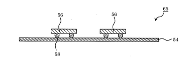
- FIG. 16 is a front sectional view of a stacked body 65 in which a plurality of semiconductor chips 56 are mounted on a mounting substrate 54.
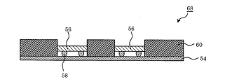
- FIG. 17 is a front cross-sectional view illustrating a state in which the sealing sheet 60 is disposed on the stacked body 65.
- seat 60 for sealing and forms the sealing layer 52 is mentioned. Note that the order of the steps A3 to E3 is not particularly limited within a possible range. In addition, unnecessary steps may be omitted as appropriate, and necessary steps may be added.
- a sealing sheet 60 having a through hole 62d is prepared (step A3).
- the sealing sheet 60 has a shape in which a plurality of through holes 62d are formed in a flat plate-like portion 62a.
- the through hole 62d is formed according to the arrangement of the plurality of semiconductor chips 56 to be sealed.
- the case where the side surface of the plate-like portion 62a is in contact with the side surface of the semiconductor chip 56 will be described. However, in the present invention, it may not be in contact.
- the constituent material of the sealing sheet 60 can be the same as that of the sealing sheet 20.
- Examples of the method for producing the sealing sheet 60 include a method of forming the through hole 62d by punching or the like after the flat plate-like portion 62a having no through hole is created.
- a stacked body 65 in which a plurality of semiconductor chips 56 are mounted on a mounting substrate 54 is prepared (step B3).
- the sealing sheet 60 is disposed on the stacked body 65 so that the entire upper surface 56a of the semiconductor chip 56 is exposed from the through hole 62d (step C3). That is, the shape of the through hole 62 d of the sealing sheet 60 is formed in the same shape in plan view so as to correspond to the semiconductor chip 56.
- sealing body forming process Next, for example, the sealing sheet 60 is fixed to the mounting substrate 54 by hot pressing with a lower heating plate and an upper heating plate (not shown). Thereby, the sealing body 68 in which the semiconductor chip 56 is sealed with the sealing sheet 60 is formed (step D3).
- the sealing sheet 60 is thermally cured to form the sealing layer 52 (step E3). Specifically, for example, the entire sealing body 68 is heated. Thus, the electronic device package 50 (see FIG. 3) is obtained.
- the sealed body of the present invention is a semiconductor chip
- the sealed body of the present invention is not limited to this example.
- various electronic components other than the semiconductor chip for example, a capacitor, a resistor, etc. may be used.
- the third embodiment when it is not contacting the sealing layer in the whole upper surface and side surface of a to-be-sealed body, in 2nd Embodiment, it seals in a part of upper surface of a to-be-sealed body, and a part of side surface
- the third embodiment has described the case where the entire upper surface of the object to be sealed is not in contact with the sealing layer.
- the present invention is not limited to this example.
- at least a part of the upper surface and the side surface of the object to be sealed may have a non-contact portion that is not in contact with the sealing layer.
Landscapes
- Physics & Mathematics (AREA)
- Acoustics & Sound (AREA)
- Structures Or Materials For Encapsulating Or Coating Semiconductor Devices Or Solid State Devices (AREA)
- Surface Acoustic Wave Elements And Circuit Networks Thereof (AREA)
Abstract
被封止体と、被封止体を封止する封止層とを備え、被封止体は、被封止体の上面及び側面のうちの少なくとも一部において、封止層と接触していない部分を有する電子デバイスパッケージ。
Description
本発明は、電子デバイスパッケージ、及び、封止用シートに関する。
従来、MEMS(Micro Electro Mechanical Systems)や、SAW(Surface Acoustic Wave)フィルターなどの可動部を有する機能素子がバンプ形成面に形成された半導体チップが存在する。このような半導体チップは、可動部を封止樹脂等で覆うことができない。そのため、可動部が搭載基板と対向するように半導体チップを搭載用基板にフリップチップ接続し、半導体チップの可動部と搭載用基板との間を中空構造としている。
従来、半導体チップと搭載用基板との間が中空構造となっている中空型電子デバイスを樹脂封止して中空型電子デバイスパッケージを作製する際に、封止樹脂としてシート状のものが用いられることがある(例えば、特許文献1参照)。
機能素子が搭載用基板と対向する側の面に形成されている場合であれば、上述したようなシート状の封止樹脂を用いて中空型電子デバイスパッケージを製造することができる。
しかしながら、機能素子を、搭載用基板とは対向しない側の面に配置したい場合、機能素子に封止樹脂が触れてしまうことになるため、上述のようなシート状の封止樹脂を用いて中空型電子デバイスパッケージを製造することはできない。
本発明は上述した課題に鑑みてなされたものであり、上面又は側面が封止層と接触していない部分を有する電子デバイスパッケージを提供することにある。また、当該電子デバイスパッケージを製造するのに利用できる封止用シートを提供することにある。
本願発明者等は、下記の構成を採用することにより、前記の課題を解決できることを見出して本発明を完成させるに至った。
すなわち、本発明は、電子デバイスパッケージであって、
被封止体と、
前記被封止体を封止する封止層と
を備え、
前記被封止体は、前記被封止体の上面及び側面のうちの少なくとも一部において、前記封止層と接触していない非接触部を有することを特徴とする。
被封止体と、
前記被封止体を封止する封止層と
を備え、
前記被封止体は、前記被封止体の上面及び側面のうちの少なくとも一部において、前記封止層と接触していない非接触部を有することを特徴とする。
本発明に係る電子デバイスパッケージによれば、被封止体が、被封止体の上面及び側面のうちの少なくとも一部において、封止層と接触していない非接触部を有する新たな形状の電子デバイスパッケージを提供することができる。
本明細書において、電子デバイスパッケージは、被封止体の一部又は全体を取り囲むように封止層が形成されていればよく、被封止体の一部が露出していてもよい。また、被封止体の一部又は全体が封止層に取り囲まれていればよく、被封止体と封止層とは接触していても接触していなくてもよい。
前記構成において、前記被封止体の上面には、可動部を有する機能素子が形成されており、
前記被封止体は、少なくとも前記機能素子が形成されている部分において、前記封止層と接触していない非接触部を有することが好ましい。
前記被封止体は、少なくとも前記機能素子が形成されている部分において、前記封止層と接触していない非接触部を有することが好ましい。
前記構成によれば、被封止体の上面に機能素子が形成されている場合に、機能素子の可動部を封止層に接触させない。すなわち、前記構成によれば、被封止体の上面に、可動部を有する機能素子が形成されている形態の電子デバイスパッケージとすることができる。
また、前記構成において、前記被封止体の上面には、光電変換素子が形成されており、
前記被封止体は、少なくとも前記光電変換素子が形成されている部分において、前記封止層と接触していない非接触部を有することも好ましい。
前記被封止体は、少なくとも前記光電変換素子が形成されている部分において、前記封止層と接触していない非接触部を有することも好ましい。
前記構成によれば、被封止体の上面に光電変換素子が形成されている場合に、光電変換素子を封止層に接触させない。すなわち、前記構成によれば、被封止体の上面に、光電変換素子が形成されている形態の電子デバイスパッケージとすることができる。
前記構成において、前記封止層は、シート状の封止用シートを用いて形成されたものであることが好ましい。
本明細書において「シート状の封止用シート」とは、シートの形態を有する封止用シートをいい、凹部や孔が形成されているシートを含む。
仮に、前記封止層を、液状の封止用樹脂を用いて形成しようとすると、被封止体の上面及び側面に接触させずに、被封止体を封止することは困難である。また、仮に、前記封止層を、ペレット状の樹脂を用いて圧縮成形にて形成しようとすると、被封止体の上面及び側面に接触させずに、被封止体を封止することは困難である。一方、前記構成によれば、前記封止層が、シート状の封止用シートを用いて形成されたものであるため、例えば、シート状の封止用シートに凹部や貫通孔を設ければ、前記電子デバイスパッケージを製造し易い。
また、本発明に係る封止用シートによれば、凹部又は貫通孔が複数形成されていることを特徴とする。
本発明に係る封止用シートによれば、凹部又は貫通孔が複数形成されている。従って、例えば、複数の被封止体を一括封止する際に、複数の被封止体と複数の前記凹部又は前記貫通孔の位置とが対応するように被封止体上に封止用シートを配置した後、平板プレス等すれば、被封止体の上面及び側面のうちの少なくとも一部において、封止用シートと接触させない形態で被封止体を封止することができる。
本発明によれば、上面又は側面が封止層と接触していない部分を有する電子デバイスパッケージを提供することができる。また、当該電子デバイスパッケージを製造するのに利用できる封止用シートを提供することができる。
以下、本発明の実施形態について、図面を参照しつつ説明する。ただし、本発明はこれらの実施形態のみに限定されるものではない。
[第1実施形態]
図1は、第1実施形態に係る電子デバイスパッケージの正面断面図である。図1に示すように、第1実施形態に係る電子デバイスパッケージ10は、搭載用基板14と、搭載用基板14にフリップチップ接続された半導体チップ16(本発明の被封止体に相当)と、半導体チップ16を封止する封止層12とを有する。封止層12は、半導体チップ16の上面16a及び側面16bのいずれにも接触しない態様で搭載用基板14上に形成されている。すなわち、電子デバイスパッケージ10は、半導体チップ16が、半導体チップ16の上面16a及び側面16bの全体において、封止層12と接触していない非接触部19を有する。
図1は、第1実施形態に係る電子デバイスパッケージの正面断面図である。図1に示すように、第1実施形態に係る電子デバイスパッケージ10は、搭載用基板14と、搭載用基板14にフリップチップ接続された半導体チップ16(本発明の被封止体に相当)と、半導体チップ16を封止する封止層12とを有する。封止層12は、半導体チップ16の上面16a及び側面16bのいずれにも接触しない態様で搭載用基板14上に形成されている。すなわち、電子デバイスパッケージ10は、半導体チップ16が、半導体チップ16の上面16a及び側面16bの全体において、封止層12と接触していない非接触部19を有する。
半導体チップ16の上面16aとは反対側の面16c(以下、バンプ形成面16cともいう)には、フリップチップ接続するためのバンプ18が形成されており、バンプ18を介して搭載用基板14に接続されている。また、上面16aには、可動部を有する機能素子が形成されている(図示せず)。前記の可動部を有する機能素子としては、特に限定されないが、MEMS(Micro Electro Mechanical Systems)、SAW(Surface Acoustic Wave)フィルター等が挙げられる。なかでも、完全に密閉されており、外部からの直接的な接触が不可能な点で、SAWフィルターや圧力センサであることが特に好ましい。半導体チップ16のバンプ形成面16cと搭載用基板14との空隙17は、用途に応じて、樹脂により封止(アンダーフィル)されていてもよく、されていなくてもよい。
搭載用基板14としては、プリント配線基板、回路が形成された半導体ウエハ等を挙げることができる。
電子デバイスパッケージ10によれば、半導体チップ16が、半導体チップ16の上面16a及び側面16bの全体において、封止層12と接触していない非接触部19を有する新たな形状の電子デバイスパッケージ10を提供することができる。
また、電子デバイスパッケージ10によれば、半導体チップ16の上面16aに機能素子が形成されており、且つ、前記機能素子の可動部を封止層12に接触させない。すなわち、前記構成によれば、半導体チップ16の上面16aに、可動部を有する機能素子が形成されている形態の電子デバイスパッケージとすることができる。
また、電子デバイスパッケージ10によれば、半導体チップ16の上面16aに機能素子が形成されており、且つ、前記機能素子の可動部を封止層12に接触させない。すなわち、前記構成によれば、半導体チップ16の上面16aに、可動部を有する機能素子が形成されている形態の電子デバイスパッケージとすることができる。
[第2実施形態]
図2は、第2実施形態に係る電子デバイスパッケージの正面断面図である。図2に示すように、第2実施形態に係る電子デバイスパッケージ30は、搭載用基板34と、搭載用基板34にフリップチップ接続された半導体チップ36(本発明の被封止体に相当)と、半導体チップ36を封止する封止層32とを有する。封止層32は、半導体チップ36の上面36aの一部及び側面36bの一部において接触せず、他の部分において接触しない態様で搭載用基板34上に形成されている。すなわち、電子デバイスパッケージ30は、半導体チップ36が、半導体チップ36の上面36aの一部及び側面36bの一部において、封止層32と接触していない非接触部39を有する。
図2は、第2実施形態に係る電子デバイスパッケージの正面断面図である。図2に示すように、第2実施形態に係る電子デバイスパッケージ30は、搭載用基板34と、搭載用基板34にフリップチップ接続された半導体チップ36(本発明の被封止体に相当)と、半導体チップ36を封止する封止層32とを有する。封止層32は、半導体チップ36の上面36aの一部及び側面36bの一部において接触せず、他の部分において接触しない態様で搭載用基板34上に形成されている。すなわち、電子デバイスパッケージ30は、半導体チップ36が、半導体チップ36の上面36aの一部及び側面36bの一部において、封止層32と接触していない非接触部39を有する。
半導体チップ36の上面36aとは反対側の面36c(以下、バンプ形成面36cともいう)には、フリップチップ接続するためのバンプ38が形成されており、バンプ38を介して搭載用基板34に接続されている。また、上面36aには、可動部を有する機能素子が形成されている(図示せず)。封止層32は、前記の可動部を有する機能素子が形成されている箇所上には、形成されていない。前記の可動部を有する機能素子としては、第1実施形態と同様、特に限定されないが、MEMS(Micro Electro Mechanical Systems)、SAW(Surface Acoustic Wave)フィルター等が挙げられる。なかでも、封止層12を介することなく直接に外部からの各種入力が可能な点で圧力センサーやジャイロセンサが特に好ましい。半導体チップ36のバンプ形成面16cと搭載用基板34との空隙37は、用途に応じて、樹脂により封止(アンダーフィル)されていてもよく、されていなくてもよい。ただし、半導体チップ16が外部に露出していることから、アンダーフィルされている方が好ましい。
搭載用基板34としては、プリント配線基板、回路が形成された半導体ウエハ等を挙げることができる。
電子デバイスパッケージ30によれば、半導体チップ36の上面36aの一部に機能素子が形成されている。そして、機能素子が形成されている部分を含む半導体チップ36の上面36aの一部及び側面36bの一部を封止層32に接触させない。すなわち、前記構成によれば、半導体チップ36の上面36aに、可動部を有する機能素子が形成されている形態の電子デバイスパッケージとすることができる。
[第3実施形態]
図3は、第3実施形態に係る電子デバイスパッケージの正面断面図である。図3に示すように、第3実施形態に係る電子デバイスパッケージ50は、搭載用基板54と、搭載用基板54にフリップチップ接続された半導体チップ56(本発明の被封止体に相当)と、半導体チップ56を封止する封止層52とを有する。封止層52は、半導体チップ56の側面56bの全体に接触し、且つ、上面56aとは接触しない態様で搭載用基板54上に形成されている。すなわち、電子デバイスパッケージ50は、半導体チップ56の上面56a全体において、封止層52と接触していない非接触部59を有する。
図3は、第3実施形態に係る電子デバイスパッケージの正面断面図である。図3に示すように、第3実施形態に係る電子デバイスパッケージ50は、搭載用基板54と、搭載用基板54にフリップチップ接続された半導体チップ56(本発明の被封止体に相当)と、半導体チップ56を封止する封止層52とを有する。封止層52は、半導体チップ56の側面56bの全体に接触し、且つ、上面56aとは接触しない態様で搭載用基板54上に形成されている。すなわち、電子デバイスパッケージ50は、半導体チップ56の上面56a全体において、封止層52と接触していない非接触部59を有する。
半導体チップ56の上面56aとは反対側の面56c(以下、バンプ形成面56cともいう)には、フリップチップ接続するためのバンプ58が形成されており、バンプ58を介して搭載用基板54に接続されている。また、上面56aには、光電変換素子が形成されている(図示せず)。前記光電変換素子としては、外部から表面56aに入射した光を電気エネルギーに変換するものであってもよく、バンプ58等から供給された電気エネルギーを光に変換して表面56aから外部へ放出するものであってもよい。半導体チップ56のバンプ形成面56cと搭載用基板54との空隙57は、樹脂により封止(アンダーフィル)されていてもよく、されていなくてもよい。なお、本実施形態では、発光効率又は受光効率を高めるため、半導体チップ56の上面56aの全体に光電変換素子が形成されている。従って、半導体チップ56の上面56aの全体が封止層によって覆わない構造としている。
搭載用基板54としては、プリント配線基板、回路が形成された半導体ウエハ等を挙げることができる。
電子デバイスパッケージ50によれば、半導体チップ56の半導体チップ56の上面56a全体において、封止層52と接触していない非接触部59を有する。すなわち、前記構成によれば、半導体チップ56の上面56aに光電変換素子が形成されている形態の電子デバイスパッケージとすることができる。
次に、電子デバイスパッケージの製造方法について説明する。
まず、電子デバイスパッケージ10の製造方法について説明する。図4~図6は、第1実施形態に係る電子デバイスパッケージの製造方法を説明するための図である。具体的に、図4(a)は、電子デバイスパッケージ10の製造に使用する封止用シート20の底面図であり、図4(b)は、その正面断面図である。図5(a)は、複数の半導体チップ16が搭載用基板14上に搭載された積層体25の正面断面図である。
電子デバイスパッケージ10の製造方法としては、
凹部22cを有する封止用シート20を準備する工程Aと、
半導体チップ16が搭載用基板14上に搭載された積層体25を準備する工程Bと、
凹部22cに半導体チップ16が配置されるように、積層体25上に封止用シート20を配置する工程Cと、
外部より圧力を加え、半導体チップ16が封止用シート20により封止された封止体28を形成する工程Dと、
封止用シート20を熱硬化させ、封止層12を形成する工程Eとを含む方法が挙げられる。
なお、工程A~工程Eは、可能な範囲内において順序は特に制限されない。また、適宜不要な工程は省略してもよく、必要な工程を追加してもよい。
凹部22cを有する封止用シート20を準備する工程Aと、
半導体チップ16が搭載用基板14上に搭載された積層体25を準備する工程Bと、
凹部22cに半導体チップ16が配置されるように、積層体25上に封止用シート20を配置する工程Cと、
外部より圧力を加え、半導体チップ16が封止用シート20により封止された封止体28を形成する工程Dと、
封止用シート20を熱硬化させ、封止層12を形成する工程Eとを含む方法が挙げられる。
なお、工程A~工程Eは、可能な範囲内において順序は特に制限されない。また、適宜不要な工程は省略してもよく、必要な工程を追加してもよい。
(封止用シートを準備する工程)
電子デバイスパッケージ10の製造方法においては、まず、図4(a)及び図4(b)に示すように、凹部22cが形成されている封止用シート20を準備する(工程A)。
電子デバイスパッケージ10の製造方法においては、まず、図4(a)及び図4(b)に示すように、凹部22cが形成されている封止用シート20を準備する(工程A)。
(封止用シート)
封止用シート20は、平板状の板状部22aと、板状部22a上に形成された、格子状の格子状部22bとを備える。板状部22a上の格子状部22bが形成されていない部分が凹部22cに相当する。
封止用シート20は、平板状の板状部22aと、板状部22a上に形成された、格子状の格子状部22bとを備える。板状部22a上の格子状部22bが形成されていない部分が凹部22cに相当する。
凹部22cは、封止する対象である複数の半導体チップ16の配置に応じて形成されている。本実施形態では、説明を容易とするため、凹部22cが4箇所形成されている場合について説明するが、本発明においてはこの例に限定されず、凹部の数は特に限定されない。また、本実施形態では、4箇所の凹部22cの形状がすべて同じである場合について説明するが、本発明においてはこの例に限定されず、異なっていてもよい。例えば、互いに大きさの異なる被封止体を封止することとし、被封止体の大きさに応じてそれぞれ凹部の大きさを異ならせることとしてもよい。
封止用シート20の構成材料は、エポキシ樹脂、及び、硬化剤としてのフェノール樹脂を含むことが好ましい。これにより、良好な熱硬化性が得られる。
前記エポキシ樹脂としては、特に限定されるものではない。例えば、トリフェニルメタン型エポキシ樹脂、クレゾールノボラック型エポキシ樹脂、ビフェニル型エポキシ樹脂、変性ビスフェノールA型エポキシ樹脂、ビスフェノールA型エポキシ樹脂、ビスフェノールF型エポキシ樹脂、変性ビスフェノールF型エポキシ樹脂、ジシクロペンタジエン型エポキシ樹脂、フェノールノボラック型エポキシ樹脂、フェノキシ樹脂などの各種のエポキシ樹脂を用いることができる。これらエポキシ樹脂は単独で用いてもよいし2種以上併用してもよい。
エポキシ樹脂の硬化後の靭性及びエポキシ樹脂の反応性を確保する観点からは、エポキシ当量150~250、軟化点もしくは融点が50~130℃の常温で固形のものが好ましく、なかでも、信頼性の観点から、トリフェニルメタン型エポキシ樹脂、クレゾールノボラック型エポキシ樹脂、ビフェニル型エポキシ樹脂がより好ましい。
前記フェノール樹脂は、エポキシ樹脂との間で硬化反応を生起するものであれば特に限定されるものではない。例えば、フェノールノボラック樹脂、フェノールアラルキル樹脂、ビフェニルアラルキル樹脂、ジシクロペンタジエン型フェノール樹脂、クレゾールノボラック樹脂、レゾール樹脂などが用いられる。これらフェノール樹脂は単独で用いてもよいし、2種以上併用してもよい。
前記フェノール樹脂としては、エポキシ樹脂との反応性の観点から、水酸基当量が70~250、軟化点が50~110℃のものを用いることが好ましく、なかでも硬化反応性が高いという観点から、フェノールノボラック樹脂を好適に用いることができる。また、信頼性の観点から、フェノールアラルキル樹脂やビフェニルアラルキル樹脂のような低吸湿性のものも好適に用いることができる。
エポキシ樹脂とフェノール樹脂の配合割合は、硬化反応性という観点から、エポキシ樹脂中のエポキシ基1当量に対して、フェノール樹脂中の水酸基の合計が0.7~1.5当量となるように配合することが好ましく、より好ましくは0.9~1.2当量である。
封止用シート20中のエポキシ樹脂及びフェノール樹脂の合計含有量は、2.5重量%以上が好ましく、3.0重量%以上がより好ましい。2.5重量%以上であると、半導体チップ16に対する接着力が良好に得られる。封止用シート20中のエポキシ樹脂及びフェノール樹脂の合計含有量は、20重量%以下が好ましく、10重量%以下がより好ましい。20重量%以下であると、吸湿性を低減できる。
封止用シート20は、熱可塑性樹脂を含むことが好ましい。これにより、未硬化時のハンドリング性や、硬化物の低応力性が得られる。
前記熱可塑性樹脂としては、天然ゴム、ブチルゴム、イソプレンゴム、クロロプレンゴム、エチレン-酢酸ビニル共重合体、エチレン-アクリル酸共重合体、エチレン-アクリル酸エステル共重合体、ポリブタジエン樹脂、ポリカーボネート樹脂、熱可塑性ポリイミド樹脂、6-ナイロンや6,6-ナイロンなどのポリアミド樹脂、フェノキシ樹脂、アクリル樹脂、PETやPBTなどの飽和ポリエステル樹脂、ポリアミドイミド樹脂、フッ素樹脂、スチレン-イソブチレン-スチレンブロック共重合体などが挙げられる。これらの熱可塑性樹脂は単独で、又は2種以上を併用して用いることができる。なかでも、低応力性、低吸水性という観点から、スチレン-イソブチレン-スチレンブロック共重合体が好ましい。
封止用シート20中の熱可塑性樹脂の含有量は、1.5重量%以上が好ましく、2.0重量%以上がより好ましい。1.5重量%以上であると、柔軟性、可撓性が得られる。封止用シート20中の熱可塑性樹脂の含有量は、6重量%以下が好ましく、4重量%以下がより好ましい。4重量%以下であると、半導体チップ16との接着性が良好である。
封止用シート20は、無機充填剤を含むことが好ましい。
前記無機充填剤は、特に限定されるものではなく、従来公知の各種充填剤を用いることができ、例えば、石英ガラス、タルク、シリカ(溶融シリカや結晶性シリカなど)、アルミナ、窒化アルミニウム、窒化珪素、窒化ホウ素の粉末が挙げられる。これらは単独で用いてもよいし、2種以上併用してもよい。なかでも、線膨張係数を良好に低減できるという理由から、シリカ、アルミナが好ましく、シリカがより好ましい。
シリカとしては、シリカ粉末が好ましく、溶融シリカ粉末がより好ましい。溶融シリカ粉末としては、球状溶融シリカ粉末、破砕溶融シリカ粉末が挙げられるが、流動性という観点から、球状溶融シリカ粉末が好ましい。なかでも、平均粒径が10~30μmの範囲のものが好ましく、15~25μmの範囲のものがより好ましい。
なお、平均粒径は、例えば、母集団から任意に抽出される試料を用い、レーザー回折散乱式粒度分布測定装置を用いて測定することにより導き出すことができる。
なお、平均粒径は、例えば、母集団から任意に抽出される試料を用い、レーザー回折散乱式粒度分布測定装置を用いて測定することにより導き出すことができる。
封止用シート20中の前記無機充填剤の含有量は、封止用シート20全体に対して、75~95重量%であることが好ましく、より好ましくは、78~95重量%である。前記無機充填剤の含有量が封止用シート20全体に対して75重量%以上であると、熱膨張率を低く抑えられることにより,熱衝撃よる機械的な破壊を抑制することができる。その結果、一方、前記無機充填剤の含有量が封止用シート20全体に対して95重量%以下であると、柔軟性、流動性、接着性がより良好となる。
封止用シート20は、硬化促進剤を含むことが好ましい。
硬化促進剤としては、エポキシ樹脂とフェノール樹脂の硬化を進行させるものであれば特に限定されず、例えば、トリフェニルホスフィン、テトラフェニルホスホニウムテトラフェニルボレートなどの有機リン系化合物;2-フェニル-4,5-ジヒドロキシメチルイミダゾール、2-フェニル-4-メチル-5-ヒドロキシメチルイミダゾールなどのイミダゾール系化合物;などが挙げられる。なかでも、混練時の温度上昇によっても硬化反応が急激に進まず、封止用シート20を良好に作製できるという理由から、2-フェニル-4,5-ジヒドロキシメチルイミダゾールが好ましい。
硬化促進剤の含有量は、エポキシ樹脂及びフェノール樹脂の合計100重量部に対して0.1~5重量部が好ましい。
封止用シート20は、難燃剤成分を含むことが好ましい。これにより、部品ショートや発熱などにより発火した際の、燃焼拡大を低減できる。難燃剤組成分としては、例えば水酸化アルミニウム、水酸化マグネシウム、水酸化鉄、水酸化カルシウム、水酸化スズ、複合化金属水酸化物などの各種金属水酸化物;ホスファゼン系難燃剤などを用いることができる。
少量でも難燃効果を発揮するという観点から、ホスファゼン系難燃剤に含まれるリン元素の含有率は、12重量%以上であることが好ましい。
封止用シート20中の難燃剤成分の含有量は、全有機成分(無機フィラーを除く)中、10重量%以上が好ましく、15重量%以上がより好ましい。10重量%以上であると、難燃性が良好に得られる。封止用シート20中の熱可塑性樹脂の含有量は、30重量%以下が好ましく、25重量%以下がより好ましい。30重量%以下であると、硬化物の物性低下(具体的には、ガラス転移温度や高温樹脂強度などの物性の低下)が少ない傾向がある。
封止用シート20は、シランカップリング剤を含むことが好ましい。シランカップリング剤としては特に限定されず、3-グリシドキシプロピルトリメトキシシランなどが挙げられる。
封止用シート20中のシランカップリング剤の含有量は、0.1~3重量%が好ましい。0.1重量%以上であると、硬化物の強度が十分得られ吸水率を低くできる。3重量%以下であると、アウトガス量を低くできる。
封止用シート20は、着色されていることが好ましい。これにより、優れたマーキング性及び外観性を発揮させることができ、付加価値のある外観の半導体装置とすることが可能になる。着色された封止用シート20は、優れたマーキング性を有しているので、マーキングを施し、文字情報や図形情報などの各種情報を付与させることができる。
封止用シート20を着色する際には、目的とする色に応じて、色材(着色剤)を用いることができる。このような色材としては、黒系色材、青系色材、赤系色材などの各種濃色系色材を好適に用いることができ、特に黒系色材が好適である。色材としては、顔料、染料などいずれであってもよい。色材は単独で又は2種以上を組み合わせて用いることができる。なお、染料としては、酸性染料、反応染料、直接染料、分散染料、カチオン染料等のいずれの形態の染料であっても用いることが可能である。また、顔料も、その形態は特に制限されず、公知の顔料から適宜選択して用いることができる。
なお、封止用シート20には、上記の各成分以外に必要に応じて、他の添加剤を適宜配合できる。
封止用シート20の厚さ(板状部22aと格子状部22bとの合計厚さ)は、特に限定されないが、少なくとも、半導体チップ16を埋め込む観点から、半導体チップ16の厚さと同一か厚いものが好ましい。封止用シートとして使用する観点から、具体的には、例えば、50μm~2000μmである。
凹部22cの深さは、封止時に半導体チップ16の上面16aに触れないようにする観点から、半導体チップ16の厚さよりも深いことが好ましい。ただし、封止時に封止用シート20全体が薄くなる場合がある。以上の観点から、半導体チップの厚さの1.05~1.40倍の深さであることが好ましい。具体的には、例えば10μm~80μmである。
封止用シート20の製造方法は特に限定されないが、平板状の樹脂シートを形成し、その後、封止用シート20に対応する形状をした金型等を用いて板状部22aと格子状部22bとを有し、且つ、凹部22cが形成された形状に一括成形する方法が挙げられる。また、ペレット状の樹脂材料を、封止用シート20に対応する形状をした金型のキャビティに入れ、圧力と熱を加えて圧縮成形する方法が挙げられる。
封止用シート20を製造するための上記の平板状の樹脂シートの製造方法は特に限定されないが、封止用シート20を形成するための樹脂組成物の混練物を調製し、得られた混練物を塗工する方法や、得られた混練物をシート状に塑性加工する方法が好ましい。これにより、溶剤を使用せずに封止用シート20を作製できるので、半導体チップ16が揮発した溶剤により影響を受けることを抑制することができる。
具体的には、後述の各成分をミキシングロール、加圧式ニーダー、押出機などの公知の混練機で溶融混練することにより混練物を調製し、得られた混練物を塗工又は塑性加工によりシート状にする。混練条件として、温度は、上述の各成分の軟化点以上であることが好ましく、例えば30~150℃、エポキシ樹脂の熱硬化性を考慮すると、好ましくは40~140℃、さらに好ましくは60~120℃である。時間は、例えば1~30分間、好ましくは5~15分間である。
混練は、減圧条件下(減圧雰囲気下)で行うことが好ましい。これにより、脱気できるとともに、混練物への気体の侵入を防止できる。減圧条件下の圧力は、好ましくは0.1kg/cm2以下、より好ましくは0.05kg/cm2以下である。減圧下の圧力の下限は特に限定されないが、例えば、1×10-4kg/cm2以上である。
混練物を塗工して上記の平板状の樹脂シートを形成する場合、溶融混練後の混練物は、冷却することなく高温状態のままで塗工することが好ましい。塗工方法としては特に制限されず、バーコート法、ナイフコート法,スロットダイ法等を挙げることができる。塗工時の温度としては、上述の各成分の軟化点以上が好ましく、エポキシ樹脂の熱硬化性および成形性を考慮すると、例えば40~150℃、好ましくは50~140℃、さらに好ましくは70~120℃である。
混練物を塑性加工して上記の平板状の樹脂シートを形成する場合、溶融混練後の混練物は、冷却することなく高温状態のままで塑性加工することが好ましい。塑性加工方法としては特に制限されず、平板プレス法、Tダイ押出法、スクリューダイ押出法、ロール圧延法、ロール混練法、インフレーション押出法、共押出法、カレンダー成形法などなどが挙げられる。塑性加工温度としては上述の各成分の軟化点以上が好ましく、エポキシ樹脂の熱硬化性および成形性を考慮すると、例えば40~150℃、好ましくは50~140℃、さらに好ましくは70~120℃である。なお、混練物を塑性加工して直接に封止用シート20の形状としてもよい。
なお、上記の平板状の樹脂シートは、適当な溶剤に封止用シート20を形成するための樹脂等を溶解、分散させてワニスを調整し、このワニスを塗工して得ることもできる。
(積層体準備工程)
また、電子デバイスパッケージ10の製造方法においては、図5に示すように、複数の半導体チップ16が搭載用基板14上に搭載された積層体25を準備する(工程B)。半導体チップ16の搭載用基板14への搭載には、フリップチップボンダーやダイボンダーなどの公知の装置を用いることができる。半導体チップ16と搭載用基板14とはバンプ18を介して電気的に接続されている。
また、電子デバイスパッケージ10の製造方法においては、図5に示すように、複数の半導体チップ16が搭載用基板14上に搭載された積層体25を準備する(工程B)。半導体チップ16の搭載用基板14への搭載には、フリップチップボンダーやダイボンダーなどの公知の装置を用いることができる。半導体チップ16と搭載用基板14とはバンプ18を介して電気的に接続されている。
(封止用シート配置工程)
次に、図6に示すように、凹部22cに半導体チップ16が配置されるように、積層体25上に封止用シート20を配置する(工程C)。この際、半導体チップ16の上面16a及び側面16bに封止用シート20が触れないように配置する。
次に、図6に示すように、凹部22cに半導体チップ16が配置されるように、積層体25上に封止用シート20を配置する(工程C)。この際、半導体チップ16の上面16a及び側面16bに封止用シート20が触れないように配置する。
(封止体形成工程)
次に、例えば、図示しない下側加熱板と上側加熱板とにより熱プレスして、搭載用基板14に封止用シート20を固定する。これにより、封止体28を形成する(工程D)。
次に、例えば、図示しない下側加熱板と上側加熱板とにより熱プレスして、搭載用基板14に封止用シート20を固定する。これにより、封止体28を形成する(工程D)。
この際の熱プレス条件としては、温度が、例えば、40~150℃、好ましくは60~120℃であり、圧力が、例えば、0.1~10MPa、好ましくは0.5~8MPaである。また、封止用シート20の搭載用基板14への密着性および追従性の向上を考慮すると、減圧条件下においてプレスすることが好ましい。前記減圧条件としては、例えば、0.1~5kPa、より好ましくは、0.1~100Paである。
(熱硬化工程)
次に、封止用シート20を熱硬化させ、封止層12を形成する(工程E)。具体的には、例えば、封止体28全体を加熱する。以上により、電子デバイスパッケージ10(図1参照)が得られる。
次に、封止用シート20を熱硬化させ、封止層12を形成する(工程E)。具体的には、例えば、封止体28全体を加熱する。以上により、電子デバイスパッケージ10(図1参照)が得られる。
熱硬化処理の条件として、加熱温度が好ましくは100℃以上、より好ましくは120℃以上である。一方、加熱温度の上限が、好ましくは200℃以下、より好ましくは180℃以下である。加熱時間が、好ましくは10分以上、より好ましくは30分以上である。一方、加熱時間の上限が、好ましくは180分以下、より好ましくは120分以下である。また、必要に応じて加圧してもよく、好ましくは0.1MPa以上、より好ましくは0.5MPa以上である。一方、上限は好ましくは10MPa以下、より好ましくは5MPa以下である。
なお、必要に応じて、電子デバイスパッケージ10を、半導体チップ16の1単位ごとにダイシングしてもよい。これにより、1つの半導体チップ16が封止された電子デバイスパッケージとすることができる。
上述した実施形態では、封止用シート20を準備する工程(工程A)において、板状部22aと格子状部22bとが一体的に形成された封止用シート20を準備する場合について説明した。しかしながら、本発明において封止用シートは、板状部22aと格子状部22bとを別々に作成しておき、これらを圧着して封止用シート20としてもよい。以下、この例について説明する。
図7~図9は、封止用シートの他の製造方法を説明するための図である。具体的に、図7(a)は、封止用シート20の製造に使用する板状部22aの底面図であり、図7(b)は、その正面断面図である。図8(a)は、封止用シート20の製造に使用する格子状部22bの底面図であり、図8(b)は、その正面断面図である。図9は、板状部22aと格子状部22bとの正面断面図であり、両者を圧着する様子を示している。
本実施形態においては、まず、板状部22aを作成する(図7(a)及び図7(b)参照)。また、格子状部22bを作成する(図8(a)及び図8(b)参照)。
板状部22aの作成方法としては、封止用シート20を形成するための樹脂組成物の混練物を調製し、得られた混練物を塗工する方法や、得られた混練物をシート状に塑性加工する方法が好ましい。また、適当な溶剤に封止用シート20を形成するための樹脂等を溶解、分散させてワニスを調整し、このワニスを塗工して得ることもできる。
格子状部22bの作成方法としては、封止用シート20を形成するための樹脂組成物を用いて平板状の樹脂シートを形成し、その後、凹部22cとなる箇所を打ち抜くことにより得ることができる。
次に、図9に示すように、板状部22aと格子状部22bとを圧着する。これによりこ、封止用シート20を得ることができる。
以上、封止用シート20の他の製造方法を説明した。
以上、封止用シート20の他の製造方法を説明した。
上述した実施形態では、凹部22cが形成された封止用シート20を用いて電子デバイスパッケージ10を製造する場合について説明した。しかしながら、本発明はこの例に限定されない。
図10及び図11は、第1実施形態に係る電子デバイスパッケージ10の他の製造方法を説明するための正面断面図である。
本実施形態では、複数の半導体チップ16が搭載用基板14上に搭載された積層体25(図5参照)を準備する。
次に、積層体25上に、別途に作成した格子状部22b(図8参照)を配置する(図10)。この際、搭載用基板14上に格子状部22bが載置されるように配置し、半導体チップ16に格子状部22bが触れないように配置する。
次に、格子状部22b上に、別途に作成した板状部22aを配置する(図11参照)。
その後、例えば、図示しない下側加熱板と上側加熱板とにより熱プレスして、搭載用基板14に格子状部22bと板状部22aとを固定する。その後、格子状部22bと板状部22aとを熱硬化させ、封止層12を形成する。
以上によっても、電子デバイスパッケージ10(図1参照)が得られる。
以上によっても、電子デバイスパッケージ10(図1参照)が得られる。
次に、第2実施形態に係る電子デバイスパッケージ30の製造方法について説明する。
図12~図14は、第2実施形態に係る電子デバイスパッケージの製造方法を説明するための図である。具体的に、図12(a)は、電子デバイスパッケージ30の製造に使用する封止用シート40の底面図であり、図12(b)は、その正面断面図である。図13は、複数の半導体チップ36が搭載用基板34上に搭載された積層体45の正面断面図である。図14は、積層体45上に封止用シート40を配置した様子を示す正面断面図である。
電子デバイスパッケージ30の製造方法としては、
凹部42c及び凹部42cに形成された貫通孔42dを有する封止用シート40を準備する工程A2と、
半導体チップ36が搭載用基板34上に搭載された積層体45を準備する工程B2と、
貫通孔42dから半導体チップ36の上面36aの一部が露出し、且つ、凹部42cに半導体チップ36が配置されるように、積層体45上に封止用シート40を配置する工程C2と、
外部より圧力を加え、半導体チップ36が封止用シート40により封止された封止体48を形成する工程D2と、
封止用シート40を熱硬化させ、封止層32を形成する工程E2とを含む方法が挙げられる。
なお、工程A2~工程E2は、可能な範囲内において順序は特に制限されない。また、適宜不要な工程は省略してもよく、必要な工程を追加してもよい。
凹部42c及び凹部42cに形成された貫通孔42dを有する封止用シート40を準備する工程A2と、
半導体チップ36が搭載用基板34上に搭載された積層体45を準備する工程B2と、
貫通孔42dから半導体チップ36の上面36aの一部が露出し、且つ、凹部42cに半導体チップ36が配置されるように、積層体45上に封止用シート40を配置する工程C2と、
外部より圧力を加え、半導体チップ36が封止用シート40により封止された封止体48を形成する工程D2と、
封止用シート40を熱硬化させ、封止層32を形成する工程E2とを含む方法が挙げられる。
なお、工程A2~工程E2は、可能な範囲内において順序は特に制限されない。また、適宜不要な工程は省略してもよく、必要な工程を追加してもよい。
(封止用シートを準備する工程)
電子デバイスパッケージ30の製造方法においては、まず、図12(a)及び図12(b)に示すように、凹部42cが形成され、さらに、凹部42cに貫通孔42dが形成された封止用シート40を準備する(工程A2)。
電子デバイスパッケージ30の製造方法においては、まず、図12(a)及び図12(b)に示すように、凹部42cが形成され、さらに、凹部42cに貫通孔42dが形成された封止用シート40を準備する(工程A2)。
(封止用シート)
封止用シート40は、一部に貫通孔42dを有する平板状の板状部42aと、板状部42a上に形成された、格子状の格子状部42bとを備える。板状部22a上の格子状部22bが形成されていない部分が凹部42cに相当する。
封止用シート40は、一部に貫通孔42dを有する平板状の板状部42aと、板状部42a上に形成された、格子状の格子状部42bとを備える。板状部22a上の格子状部22bが形成されていない部分が凹部42cに相当する。
凹部42cは、封止する対象である複数の半導体チップ36の配置に応じて形成されている。なお、本実施形態では、板状部42aの一部が半導体チップ36の上面に接している場合について説明するが、本発明においては接していなくてもよい。
封止用シート40の構成材料は、封止用シート20と同様とすることができる。
また、封止用シート40の製造方法も封止用シート20と同様とすることができる。例えば、封止用シート40を形成するための樹脂組成物から一体的に形成してもよいし、板状部42aを形成した後、打ち抜き等により貫通孔42dを形成し、その後、別途に作成した格子状部42bとを圧着等により貼り合わせて作成することができる。
(積層体準備工程)
また、電子デバイスパッケージ30の製造方法においては、図13に示すように、複数の半導体チップ36が搭載用基板34上に搭載された積層体45を準備する(工程B2)。
また、電子デバイスパッケージ30の製造方法においては、図13に示すように、複数の半導体チップ36が搭載用基板34上に搭載された積層体45を準備する(工程B2)。
(封止用シート配置工程)
次に、図14に示すように、貫通孔42dから半導体チップ36の上面36aの一部が露出し、且つ、凹部42cに半導体チップ36が配置されるように、積層体45上に封止用シート40を配置する(工程C2)。この際、半導体チップ36の上面36aに形成されている機能素子が貫通孔42dから露出するように配置する。
次に、図14に示すように、貫通孔42dから半導体チップ36の上面36aの一部が露出し、且つ、凹部42cに半導体チップ36が配置されるように、積層体45上に封止用シート40を配置する(工程C2)。この際、半導体チップ36の上面36aに形成されている機能素子が貫通孔42dから露出するように配置する。
(封止体形成工程)
次に、例えば、図示しない下側加熱板と上側加熱板とにより熱プレスして、搭載用基板34に封止用シート40を固定する。これにより、半導体チップ36が封止用シート40により封止された封止体48を形成する(工程D2)。
次に、例えば、図示しない下側加熱板と上側加熱板とにより熱プレスして、搭載用基板34に封止用シート40を固定する。これにより、半導体チップ36が封止用シート40により封止された封止体48を形成する(工程D2)。
(熱硬化工程)
次に、封止用シート40を熱硬化させ、封止層32を形成する(工程E2)。具体的には、例えば、封止体48全体を加熱する。以上により、電子デバイスパッケージ30(図2参照)が得られる。
次に、封止用シート40を熱硬化させ、封止層32を形成する(工程E2)。具体的には、例えば、封止体48全体を加熱する。以上により、電子デバイスパッケージ30(図2参照)が得られる。
次に、第3実施形態に係る電子デバイスパッケージ50の製造方法について説明する。
図15~図17は、第3実施形態に係る電子デバイスパッケージの製造方法を説明するための図である。具体的に、図15(a)は、電子デバイスパッケージ50の製造に使用する封止用シート60の底面図であり、図15(b)は、その正面断面図である。図16は、複数の半導体チップ56が搭載用基板54上に搭載された積層体65の正面断面図である。図17は、積層体65上に封止用シート60を配置した様子を示す正面断面図である。
電子デバイスパッケージ50の製造方法としては、
貫通孔62dを有する封止用シート60を準備する工程A3と、
半導体チップ56が搭載用基板54上に搭載された積層体65を準備する工程B3と、
貫通孔62dから半導体チップ56の上面56aの全体が露出するように、積層体65上に封止用シート60を配置する工程C3と、
外部より圧力を加え、半導体チップ56が封止用シート60により封止された封止体68を形成する工程D3と、
封止用シート60を熱硬化させ、封止層52を形成する工程E3とを含む方法が挙げられる。
なお、工程A3~工程E3は、可能な範囲内において順序は特に制限されない。また、適宜不要な工程は省略してもよく、必要な工程を追加してもよい。
貫通孔62dを有する封止用シート60を準備する工程A3と、
半導体チップ56が搭載用基板54上に搭載された積層体65を準備する工程B3と、
貫通孔62dから半導体チップ56の上面56aの全体が露出するように、積層体65上に封止用シート60を配置する工程C3と、
外部より圧力を加え、半導体チップ56が封止用シート60により封止された封止体68を形成する工程D3と、
封止用シート60を熱硬化させ、封止層52を形成する工程E3とを含む方法が挙げられる。
なお、工程A3~工程E3は、可能な範囲内において順序は特に制限されない。また、適宜不要な工程は省略してもよく、必要な工程を追加してもよい。
(封止用シートを準備する工程)
電子デバイスパッケージ50の製造方法においては、まず、図15(a)及び図15(b)に示すように、貫通孔62dを有する封止用シート60を準備する(工程A3)。
電子デバイスパッケージ50の製造方法においては、まず、図15(a)及び図15(b)に示すように、貫通孔62dを有する封止用シート60を準備する(工程A3)。
(封止用シート)
封止用シート60は、平板状の板状部62aに複数の貫通孔62dが形成された形状を有する。
封止用シート60は、平板状の板状部62aに複数の貫通孔62dが形成された形状を有する。
貫通孔62dは、封止する対象である複数の半導体チップ56の配置に応じて形成されている。なお、本実施形態では、板状部62aの側面が半導体チップ56の側面に接している場合について説明するが、本発明においては接していなくてもよい。
封止用シート60の構成材料は、封止用シート20と同様とすることができる。
封止用シート60の製造方法としては、貫通孔のない平板状の板状部62aを作成した後、打ち抜き等により貫通孔62dを形成する方法が挙げられる。
(積層体準備工程)
また、電子デバイスパッケージ50の製造方法においては、図16に示すように、複数の半導体チップ56が搭載用基板54上に搭載された積層体65を準備する(工程B3)。
また、電子デバイスパッケージ50の製造方法においては、図16に示すように、複数の半導体チップ56が搭載用基板54上に搭載された積層体65を準備する(工程B3)。
(封止用シート配置工程)
次に、図17に示すように、貫通孔62dから半導体チップ56の上面56aの全部が露出するように、積層体65上に封止用シート60を配置する(工程C3)。すなわち、封止用シート60の貫通孔62dの形状は、半導体チップ56と対応するように平面視で同じ形状に形成されている。
次に、図17に示すように、貫通孔62dから半導体チップ56の上面56aの全部が露出するように、積層体65上に封止用シート60を配置する(工程C3)。すなわち、封止用シート60の貫通孔62dの形状は、半導体チップ56と対応するように平面視で同じ形状に形成されている。
(封止体形成工程)
次に、例えば、図示しない下側加熱板と上側加熱板とにより熱プレスして、搭載用基板54に封止用シート60を固定する。これにより、半導体チップ56が封止用シート60により封止された封止体68を形成する(工程D3)。
次に、例えば、図示しない下側加熱板と上側加熱板とにより熱プレスして、搭載用基板54に封止用シート60を固定する。これにより、半導体チップ56が封止用シート60により封止された封止体68を形成する(工程D3)。
(熱硬化工程)
次に、封止用シート60を熱硬化させ、封止層52を形成する(工程E3)。具体的には、例えば、封止体68全体を加熱する。以上により、電子デバイスパッケージ50(図3参照)が得られる。
次に、封止用シート60を熱硬化させ、封止層52を形成する(工程E3)。具体的には、例えば、封止体68全体を加熱する。以上により、電子デバイスパッケージ50(図3参照)が得られる。
上述した実施形態では、本発明の被封止体が半導体チップである場合について説明したが本発明の被封止体は、この例に限定されない。例えば、半導体チップ以外の各種の電子部品(例えば、コンデンサーや抵抗等)であってもよい。
第1実施形態では、被封止体の上面及び側面の全体において封止層と接触していない場合、第2実施形態では、被封止体の上面の一部及び側面の一部において封止層と接触していない場合、第3実施形態では、被封止体の上面の全体において封止層と接触していない場合について説明した。しかしながら、本発明はこの例に限定されない。本発明においては、被封止体の上面及び側面のうちの少なくとも一部において、封止層と接触していない非接触部を有していればよい。
以上、本発明の実施形態を説明したが、具体例を例示したに過ぎず、特に本発明を限定するものではなく、各具体的構成は、適宜設計変更可能である。また、本発明の実施形態に記載された効果は、本発明から生じる最も好適な効果を列挙したに過ぎず、本発明による効果は、本発明の実施形態に記載されたものに限定されるものではない。
10、30、50 電子デバイスパッケージ
12、32、52 封止層
14、34、54 搭載用基板
16、36、56 半導体チップ(被封止体)
16a、36a、56a 半導体チップの上面
16b、36b、56b 半導体チップの側面
16c、36c、56c 半導体チップの上面とは反対側の面(バンプ形成面)
17、37、57 空隙
18、38、58 バンプ
19、39、59 非接触部
20、40、60 封止用シート
22a、42a、62a 板状部
22b、42b 格子状部
22c、42c 凹部
42d、62d 貫通孔
25、45、65 積層体
28、48、68 封止体
12、32、52 封止層
14、34、54 搭載用基板
16、36、56 半導体チップ(被封止体)
16a、36a、56a 半導体チップの上面
16b、36b、56b 半導体チップの側面
16c、36c、56c 半導体チップの上面とは反対側の面(バンプ形成面)
17、37、57 空隙
18、38、58 バンプ
19、39、59 非接触部
20、40、60 封止用シート
22a、42a、62a 板状部
22b、42b 格子状部
22c、42c 凹部
42d、62d 貫通孔
25、45、65 積層体
28、48、68 封止体
Claims (5)
- 被封止体と、
前記被封止体を封止する封止層と
を備え、
前記被封止体は、前記被封止体の上面及び側面のうちの少なくとも一部において、前記封止層と接触していない部分を有することを特徴とする電子デバイスパッケージ。 - 前記被封止体の上面には、可動部を有する機能素子が形成されており、
前記被封止体は、少なくとも前記機能素子が形成されている部分において、前記封止層と接触していない部分を有することを特徴とする請求項1に記載の電子デバイスパッケージ。 - 前記被封止体の上面には、光電変換素子が形成されており、
前記被封止体は、少なくとも前記光電変換素子が形成されている部分において、前記封止層と接触していない部分を有することを特徴とする請求項1に記載の電子デバイスパッケージ。 - 前記封止層は、シート状の封止用シートを用いて形成されたものであることを特徴とする請求項1~3のいずれか1に記載の電子デバイスパッケージ。
- 凹部又は貫通孔が複数形成されていることを特徴とする封止用シート。
Applications Claiming Priority (2)
| Application Number | Priority Date | Filing Date | Title |
|---|---|---|---|
| JP2014-251653 | 2014-12-12 | ||
| JP2014251653A JP2016115741A (ja) | 2014-12-12 | 2014-12-12 | 電子デバイスパッケージ、及び、封止用シート |
Publications (1)
| Publication Number | Publication Date |
|---|---|
| WO2016092964A1 true WO2016092964A1 (ja) | 2016-06-16 |
Family
ID=56107159
Family Applications (1)
| Application Number | Title | Priority Date | Filing Date |
|---|---|---|---|
| PCT/JP2015/080420 Ceased WO2016092964A1 (ja) | 2014-12-12 | 2015-10-28 | 電子デバイスパッケージ、及び、封止用シート |
Country Status (3)
| Country | Link |
|---|---|
| JP (1) | JP2016115741A (ja) |
| TW (1) | TW201630132A (ja) |
| WO (1) | WO2016092964A1 (ja) |
Cited By (1)
| Publication number | Priority date | Publication date | Assignee | Title |
|---|---|---|---|---|
| CN113272949A (zh) * | 2018-12-27 | 2021-08-17 | 住友电木株式会社 | 中空封装体及其制造方法 |
Citations (3)
| Publication number | Priority date | Publication date | Assignee | Title |
|---|---|---|---|---|
| JP2004255487A (ja) * | 2003-02-25 | 2004-09-16 | Nippon Telegr & Teleph Corp <Ntt> | Memsの製造方法 |
| WO2014024786A1 (ja) * | 2012-08-07 | 2014-02-13 | ポリマテック株式会社 | 熱拡散性遮音シートおよび熱拡散性遮音構造 |
| JP2014183096A (ja) * | 2013-03-18 | 2014-09-29 | Nitto Denko Corp | 貼着装置および電子装置の製造方法 |
-
2014
- 2014-12-12 JP JP2014251653A patent/JP2016115741A/ja active Pending
-
2015
- 2015-10-28 WO PCT/JP2015/080420 patent/WO2016092964A1/ja not_active Ceased
- 2015-12-07 TW TW104140975A patent/TW201630132A/zh unknown
Patent Citations (3)
| Publication number | Priority date | Publication date | Assignee | Title |
|---|---|---|---|---|
| JP2004255487A (ja) * | 2003-02-25 | 2004-09-16 | Nippon Telegr & Teleph Corp <Ntt> | Memsの製造方法 |
| WO2014024786A1 (ja) * | 2012-08-07 | 2014-02-13 | ポリマテック株式会社 | 熱拡散性遮音シートおよび熱拡散性遮音構造 |
| JP2014183096A (ja) * | 2013-03-18 | 2014-09-29 | Nitto Denko Corp | 貼着装置および電子装置の製造方法 |
Cited By (3)
| Publication number | Priority date | Publication date | Assignee | Title |
|---|---|---|---|---|
| CN113272949A (zh) * | 2018-12-27 | 2021-08-17 | 住友电木株式会社 | 中空封装体及其制造方法 |
| US20220068737A1 (en) * | 2018-12-27 | 2022-03-03 | Sumitomo Bakelite Co., Ltd. | Hollow Package And Method For Manufacturing Same |
| CN113272949B (zh) * | 2018-12-27 | 2025-04-25 | 住友电木株式会社 | 中空封装体及其制造方法 |
Also Published As
| Publication number | Publication date |
|---|---|
| TW201630132A (zh) | 2016-08-16 |
| JP2016115741A (ja) | 2016-06-23 |
Similar Documents
| Publication | Publication Date | Title |
|---|---|---|
| JP5735036B2 (ja) | 電子部品装置の製造方法、及び、積層シート | |
| CN105431937B (zh) | 密封用片、以及使用了该密封用片的半导体装置的制造方法 | |
| WO2014156837A1 (ja) | 中空封止用樹脂シート及び中空パッケージの製造方法 | |
| WO2014014008A1 (ja) | 封止層被覆半導体素子および半導体装置の製造方法 | |
| JP2013145839A (ja) | 中空封止用樹脂シートおよびその製法、並びに中空型電子部品装置の製法および中空型電子部品装置 | |
| TW201532151A (zh) | 半導體封裝之製造方法 | |
| WO2014188826A1 (ja) | 電子部品装置の製造方法 | |
| JP2016096308A (ja) | 半導体装置の製造方法 | |
| JP6302693B2 (ja) | 中空封止用樹脂シート及び中空パッケージの製造方法 | |
| WO2016092964A1 (ja) | 電子デバイスパッケージ、及び、封止用シート | |
| JP7471940B2 (ja) | 封止用樹脂シート | |
| JP7542341B2 (ja) | 封止用樹脂シートおよび封止用多層樹脂シート | |
| JP2018198337A (ja) | 中空封止用樹脂シート及び中空パッケージの製造方法 | |
| CN106796922A (zh) | 密封用片 | |
| TW201501216A (zh) | 電子零件裝置之製造方法 | |
| WO2014156777A1 (ja) | 中空型電子デバイス封止用シート、及び、中空型電子デバイスパッケージの製造方法 | |
| JP6677966B2 (ja) | セパレータ付き封止用シート、及び、半導体装置の製造方法 | |
| WO2014188824A1 (ja) | 電子部品装置の製造方法 | |
| JP7576545B2 (ja) | 封止用樹脂シート | |
| JP6630861B2 (ja) | セパレータ付き封止用シート、及び、半導体装置の製造方法 | |
| TWI643890B (zh) | Resin sheet for hollow sealing and manufacturing method of hollow package | |
| JP2015220350A (ja) | 半導体装置の製造方法 | |
| JP2015076553A (ja) | 電子デバイスパッケージの製造方法及び電子デバイスの封止方法 | |
| TW202111074A (zh) | 密封用樹脂片材 | |
| JP2018133589A (ja) | 中空型電子デバイス封止用シート、及び、中空型電子デバイスパッケージの製造方法 |
Legal Events
| Date | Code | Title | Description |
|---|---|---|---|
| 121 | Ep: the epo has been informed by wipo that ep was designated in this application |
Ref document number: 15867024 Country of ref document: EP Kind code of ref document: A1 |
|
| NENP | Non-entry into the national phase |
Ref country code: DE |
|
| 122 | Ep: pct application non-entry in european phase |
Ref document number: 15867024 Country of ref document: EP Kind code of ref document: A1 |