WO2016084563A1 - 蓄電装置 - Google Patents
蓄電装置 Download PDFInfo
- Publication number
- WO2016084563A1 WO2016084563A1 PCT/JP2015/081061 JP2015081061W WO2016084563A1 WO 2016084563 A1 WO2016084563 A1 WO 2016084563A1 JP 2015081061 W JP2015081061 W JP 2015081061W WO 2016084563 A1 WO2016084563 A1 WO 2016084563A1
- Authority
- WO
- WIPO (PCT)
- Prior art keywords
- electrode assembly
- covering material
- case
- power storage
- storage device
- Prior art date
- Legal status (The legal status is an assumption and is not a legal conclusion. Google has not performed a legal analysis and makes no representation as to the accuracy of the status listed.)
- Ceased
Links
Images


Classifications
-
- H—ELECTRICITY
- H01—ELECTRIC ELEMENTS
- H01G—CAPACITORS; CAPACITORS, RECTIFIERS, DETECTORS, SWITCHING DEVICES, LIGHT-SENSITIVE OR TEMPERATURE-SENSITIVE DEVICES OF THE ELECTROLYTIC TYPE
- H01G11/00—Hybrid capacitors, i.e. capacitors having different positive and negative electrodes; Electric double-layer [EDL] capacitors; Processes for the manufacture thereof or of parts thereof
- H01G11/78—Cases; Housings; Encapsulations; Mountings
- H01G11/82—Fixing or assembling a capacitive element in a housing, e.g. mounting electrodes, current collectors or terminals in containers or encapsulations
-
- H—ELECTRICITY
- H01—ELECTRIC ELEMENTS
- H01G—CAPACITORS; CAPACITORS, RECTIFIERS, DETECTORS, SWITCHING DEVICES, LIGHT-SENSITIVE OR TEMPERATURE-SENSITIVE DEVICES OF THE ELECTROLYTIC TYPE
- H01G11/00—Hybrid capacitors, i.e. capacitors having different positive and negative electrodes; Electric double-layer [EDL] capacitors; Processes for the manufacture thereof or of parts thereof
- H01G11/10—Multiple hybrid or EDL capacitors, e.g. arrays or modules
- H01G11/12—Stacked hybrid or EDL capacitors
-
- H—ELECTRICITY
- H01—ELECTRIC ELEMENTS
- H01G—CAPACITORS; CAPACITORS, RECTIFIERS, DETECTORS, SWITCHING DEVICES, LIGHT-SENSITIVE OR TEMPERATURE-SENSITIVE DEVICES OF THE ELECTROLYTIC TYPE
- H01G11/00—Hybrid capacitors, i.e. capacitors having different positive and negative electrodes; Electric double-layer [EDL] capacitors; Processes for the manufacture thereof or of parts thereof
- H01G11/22—Electrodes
- H01G11/24—Electrodes characterised by structural features of the materials making up or comprised in the electrodes, e.g. form, surface area or porosity; characterised by the structural features of powders or particles used therefor
-
- H—ELECTRICITY
- H01—ELECTRIC ELEMENTS
- H01G—CAPACITORS; CAPACITORS, RECTIFIERS, DETECTORS, SWITCHING DEVICES, LIGHT-SENSITIVE OR TEMPERATURE-SENSITIVE DEVICES OF THE ELECTROLYTIC TYPE
- H01G11/00—Hybrid capacitors, i.e. capacitors having different positive and negative electrodes; Electric double-layer [EDL] capacitors; Processes for the manufacture thereof or of parts thereof
- H01G11/52—Separators
-
- H—ELECTRICITY
- H01—ELECTRIC ELEMENTS
- H01G—CAPACITORS; CAPACITORS, RECTIFIERS, DETECTORS, SWITCHING DEVICES, LIGHT-SENSITIVE OR TEMPERATURE-SENSITIVE DEVICES OF THE ELECTROLYTIC TYPE
- H01G11/00—Hybrid capacitors, i.e. capacitors having different positive and negative electrodes; Electric double-layer [EDL] capacitors; Processes for the manufacture thereof or of parts thereof
- H01G11/74—Terminals, e.g. extensions of current collectors
-
- H—ELECTRICITY
- H01—ELECTRIC ELEMENTS
- H01G—CAPACITORS; CAPACITORS, RECTIFIERS, DETECTORS, SWITCHING DEVICES, LIGHT-SENSITIVE OR TEMPERATURE-SENSITIVE DEVICES OF THE ELECTROLYTIC TYPE
- H01G11/00—Hybrid capacitors, i.e. capacitors having different positive and negative electrodes; Electric double-layer [EDL] capacitors; Processes for the manufacture thereof or of parts thereof
- H01G11/74—Terminals, e.g. extensions of current collectors
- H01G11/76—Terminals, e.g. extensions of current collectors specially adapted for integration in multiple or stacked hybrid or EDL capacitors
-
- H—ELECTRICITY
- H01—ELECTRIC ELEMENTS
- H01G—CAPACITORS; CAPACITORS, RECTIFIERS, DETECTORS, SWITCHING DEVICES, LIGHT-SENSITIVE OR TEMPERATURE-SENSITIVE DEVICES OF THE ELECTROLYTIC TYPE
- H01G11/00—Hybrid capacitors, i.e. capacitors having different positive and negative electrodes; Electric double-layer [EDL] capacitors; Processes for the manufacture thereof or of parts thereof
- H01G11/78—Cases; Housings; Encapsulations; Mountings
-
- H—ELECTRICITY
- H01—ELECTRIC ELEMENTS
- H01M—PROCESSES OR MEANS, e.g. BATTERIES, FOR THE DIRECT CONVERSION OF CHEMICAL ENERGY INTO ELECTRICAL ENERGY
- H01M10/00—Secondary cells; Manufacture thereof
- H01M10/05—Accumulators with non-aqueous electrolyte
- H01M10/052—Li-accumulators
- H01M10/0525—Rocking-chair batteries, i.e. batteries with lithium insertion or intercalation in both electrodes; Lithium-ion batteries
-
- H—ELECTRICITY
- H01—ELECTRIC ELEMENTS
- H01M—PROCESSES OR MEANS, e.g. BATTERIES, FOR THE DIRECT CONVERSION OF CHEMICAL ENERGY INTO ELECTRICAL ENERGY
- H01M10/00—Secondary cells; Manufacture thereof
- H01M10/05—Accumulators with non-aqueous electrolyte
- H01M10/058—Construction or manufacture
- H01M10/0585—Construction or manufacture of accumulators having only flat construction elements, i.e. flat positive electrodes, flat negative electrodes and flat separators
-
- H—ELECTRICITY
- H01—ELECTRIC ELEMENTS
- H01M—PROCESSES OR MEANS, e.g. BATTERIES, FOR THE DIRECT CONVERSION OF CHEMICAL ENERGY INTO ELECTRICAL ENERGY
- H01M50/00—Constructional details or processes of manufacture of the non-active parts of electrochemical cells other than fuel cells, e.g. hybrid cells
- H01M50/40—Separators; Membranes; Diaphragms; Spacing elements inside cells
- H01M50/463—Separators, membranes or diaphragms characterised by their shape
- H01M50/466—U-shaped, bag-shaped or folded
-
- H—ELECTRICITY
- H01—ELECTRIC ELEMENTS
- H01M—PROCESSES OR MEANS, e.g. BATTERIES, FOR THE DIRECT CONVERSION OF CHEMICAL ENERGY INTO ELECTRICAL ENERGY
- H01M50/00—Constructional details or processes of manufacture of the non-active parts of electrochemical cells other than fuel cells, e.g. hybrid cells
- H01M50/40—Separators; Membranes; Diaphragms; Spacing elements inside cells
- H01M50/471—Spacing elements inside cells other than separators, membranes or diaphragms; Manufacturing processes thereof
- H01M50/474—Spacing elements inside cells other than separators, membranes or diaphragms; Manufacturing processes thereof characterised by their position inside the cells
-
- H—ELECTRICITY
- H01—ELECTRIC ELEMENTS
- H01M—PROCESSES OR MEANS, e.g. BATTERIES, FOR THE DIRECT CONVERSION OF CHEMICAL ENERGY INTO ELECTRICAL ENERGY
- H01M50/00—Constructional details or processes of manufacture of the non-active parts of electrochemical cells other than fuel cells, e.g. hybrid cells
- H01M50/40—Separators; Membranes; Diaphragms; Spacing elements inside cells
- H01M50/471—Spacing elements inside cells other than separators, membranes or diaphragms; Manufacturing processes thereof
- H01M50/48—Spacing elements inside cells other than separators, membranes or diaphragms; Manufacturing processes thereof characterised by the material
- H01M50/486—Organic material
-
- H—ELECTRICITY
- H01—ELECTRIC ELEMENTS
- H01M—PROCESSES OR MEANS, e.g. BATTERIES, FOR THE DIRECT CONVERSION OF CHEMICAL ENERGY INTO ELECTRICAL ENERGY
- H01M10/00—Secondary cells; Manufacture thereof
- H01M10/04—Construction or manufacture in general
- H01M10/0413—Large-sized flat cells or batteries for motive or stationary systems with plate-like electrodes
-
- H—ELECTRICITY
- H01—ELECTRIC ELEMENTS
- H01M—PROCESSES OR MEANS, e.g. BATTERIES, FOR THE DIRECT CONVERSION OF CHEMICAL ENERGY INTO ELECTRICAL ENERGY
- H01M2220/00—Batteries for particular applications
- H01M2220/20—Batteries in motive systems, e.g. vehicle, ship, plane
-
- Y—GENERAL TAGGING OF NEW TECHNOLOGICAL DEVELOPMENTS; GENERAL TAGGING OF CROSS-SECTIONAL TECHNOLOGIES SPANNING OVER SEVERAL SECTIONS OF THE IPC; TECHNICAL SUBJECTS COVERED BY FORMER USPC CROSS-REFERENCE ART COLLECTIONS [XRACs] AND DIGESTS
- Y02—TECHNOLOGIES OR APPLICATIONS FOR MITIGATION OR ADAPTATION AGAINST CLIMATE CHANGE
- Y02E—REDUCTION OF GREENHOUSE GAS [GHG] EMISSIONS, RELATED TO ENERGY GENERATION, TRANSMISSION OR DISTRIBUTION
- Y02E60/00—Enabling technologies; Technologies with a potential or indirect contribution to GHG emissions mitigation
- Y02E60/10—Energy storage using batteries
-
- Y—GENERAL TAGGING OF NEW TECHNOLOGICAL DEVELOPMENTS; GENERAL TAGGING OF CROSS-SECTIONAL TECHNOLOGIES SPANNING OVER SEVERAL SECTIONS OF THE IPC; TECHNICAL SUBJECTS COVERED BY FORMER USPC CROSS-REFERENCE ART COLLECTIONS [XRACs] AND DIGESTS
- Y02—TECHNOLOGIES OR APPLICATIONS FOR MITIGATION OR ADAPTATION AGAINST CLIMATE CHANGE
- Y02P—CLIMATE CHANGE MITIGATION TECHNOLOGIES IN THE PRODUCTION OR PROCESSING OF GOODS
- Y02P70/00—Climate change mitigation technologies in the production process for final industrial or consumer products
- Y02P70/50—Manufacturing or production processes characterised by the final manufactured product
-
- Y—GENERAL TAGGING OF NEW TECHNOLOGICAL DEVELOPMENTS; GENERAL TAGGING OF CROSS-SECTIONAL TECHNOLOGIES SPANNING OVER SEVERAL SECTIONS OF THE IPC; TECHNICAL SUBJECTS COVERED BY FORMER USPC CROSS-REFERENCE ART COLLECTIONS [XRACs] AND DIGESTS
- Y02—TECHNOLOGIES OR APPLICATIONS FOR MITIGATION OR ADAPTATION AGAINST CLIMATE CHANGE
- Y02T—CLIMATE CHANGE MITIGATION TECHNOLOGIES RELATED TO TRANSPORTATION
- Y02T10/00—Road transport of goods or passengers
- Y02T10/60—Other road transportation technologies with climate change mitigation effect
- Y02T10/70—Energy storage systems for electromobility, e.g. batteries
Definitions
- the present invention relates to a power storage device.
- An object of the present invention is to provide a power storage device capable of suppressing movement of an electrode assembly in a case.
- An electricity storage device to solve the above problems includes an electrode assembly having electrodes stacked in layers, a case accommodating the electrode assembly, and an electrode protruding from the case and electrically connected to the electrode assembly. And a covering material interposed between the case and the electrode assembly and covering at least a part of the electrode assembly, the covering material being at an edge portion of the electrode assembly. And an extending portion extending along a projecting direction of the electrode terminal from an edge opposed to the electrode terminal, wherein a coefficient of friction between the covering material and the electrode assembly is It is larger than the coefficient of friction between the case and the covering material.
- the electrode assembly can be easily inserted into the case Can be suppressed from moving relative to the covering material.
- the covering material has an extension extending from the edge of the electrode assembly toward the electrode terminal, the movement of the entire covering material toward the electrode terminal is suppressed. it can. Therefore, movement of the electrode assembly in the case can be suppressed.
- the covering material has an inner surface in contact with the electrode assembly and an outer surface in contact with the case, and the inner surface of the covering material is a rough surface;
- the outer surface of the covering is preferably a smooth surface.
- the electrode assembly has an outer surface in contact with the covering material, and the outer surface of the electrode assembly is rougher than the inner surface of the case.
- the electrode assembly preferably includes a thickness adjusting material in contact with the covering material in the outermost layer of the electrode assembly.
- the thickness of the electrode assembly can be adjusted so that the electrode assembly and the covering material come in contact with each other. Therefore, movement of the electrode assembly in the case can be further suppressed.
- the thickness adjusting material has an outer surface in contact with the covering material, the outer surface of the thickness adjusting material is a rough surface, and the covering material is in contact with the case It is preferable that it has an outer surface, and the outer surface of the covering material is a smooth surface.
- the coefficient of friction between the case and the covering material is reduced while the coefficient of friction between the covering material and the electrode assembly is increased. It can be easy.
- the electrode assembly and the covering material are in surface contact with each other. According to this, since the electrode assembly and the covering material are in surface contact, the relative movement of the electrode assembly relative to the covering material can be suppressed over a wide range. Therefore, movement of the electrode assembly in the case can be further suppressed.
- the shape of the covering material is a bag shape, and the covering material accommodates the electrode assembly. According to this, since the covering material is in the form of a bag accommodating the electrode assembly, the electrode assembly and the covering material can be easily brought into contact with each other, and the electrode assembly moves relative to the covering material. Can be further suppressed.
- the covering material is preferably an insulating film which insulates the electrode assembly from the case. According to this, while being able to insulate an electrode assembly and a case, it can suppress that it becomes difficult to insulate because the electrode assembly moves relatively with respect to a coating material.
- the electrode assembly has a tab group, the tab group is joined to the electrode terminal, and the tab group is directed to the electrode terminal by bending itself. Preferably, movement of the electrode assembly is permitted.
- the power storage device is preferably a secondary battery. According to this, in the secondary battery, movement of the electrode assembly in the case can be suppressed.
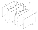
- the disassembled perspective view of a secondary battery The disassembled perspective view of an electrode assembly.
- the top view of the secondary battery of another embodiment. 5 is a cross-sectional view taken along line 5-5 of FIG.
- the secondary battery 10 as a power storage device is a lithium ion secondary battery and is a square battery whose appearance is a square shape.
- the secondary battery 10 includes a case 11 and an electrode assembly 12 accommodated in the case 11.
- the case 11 has a bottomed square cylindrical case main body 13 having an opening 14 and a square plate lid 15 closing the opening 14.
- the case body 13 and the lid 15 are made of metal such as stainless steel or aluminum, for example.
- an electrolytic solution is accommodated in the case 11 as an electrolyte (not shown).
- the electrode assembly 12 has a positive electrode 16 as an electrode, a negative electrode 17 as an electrode, and a porous separator 18 which insulates between the electrodes 16 and 17.
- the electrode assembly 12 has a stacked structure in which the positive electrode 16 and the negative electrode 17 are alternately stacked in a state in which the separator 18 is interposed therebetween.
- the electrode assembly 12 has a substantially rectangular parallelepiped shape as a whole.
- the electrode assembly 12 has an upper surface 12a opposed to the inner surface 15a of the lid 15 and a lower surface 12b opposed to the inner surface 13a of the bottom of the case main body 13 in a state accommodated in the case 11.
- the electrode assembly 12 also has side surfaces 12c, 12d, 12e, 12f connected to the surfaces 12a, 12b.
- the side surfaces 12 c and 12 d are disposed at both ends in the stacking direction T of the electrode assembly 12.
- the side surfaces 12c, 12d, 12e and 12f respectively face the side walls of the case 11 in a state where the electrode assembly 12 is housed in the case 11.
- the positive electrode 16 includes a positive electrode metal foil 19 such as aluminum, a positive electrode active material layer 20 covering the positive electrode metal foil 19, and an edge 16 a of the positive electrode metal foil 19. And a positive electrode current collecting tab 21 protruding in the surface direction.
- the positive electrode active material layer 20 is provided by applying a positive electrode active material on both surfaces of the positive electrode metal foil 19.
- the positive electrode current collection tab 21 is an uncoated portion of the positive electrode metal foil 19 to which the positive electrode active material is not applied.
- the negative electrode 17 projects from the edge 17 a of the negative electrode metal foil 22 such as copper, the negative electrode active material layer 23 covering the negative electrode metal foil 22, and the edge 17 a of the negative electrode metal foil 22 in the surface direction of the negative electrode metal foil 22. And a negative electrode current collection tab 24.
- the negative electrode active material layer 23 is provided by applying a negative electrode active material on both surfaces of the negative electrode metal foil 22.
- the negative electrode current collection tab 24 is an uncoated portion of the negative electrode metal foil 22 to which the negative electrode active material is not applied.
- the negative electrode active material layer 23 has a size capable of covering the entire surface of the positive electrode active material layer 20 when viewed in the stacking direction T in the electrode assembly 12.
- the electrode assembly 12 has the positive electrode current collection tab group 25 which protruded from the upper surface 12a, and the some positive electrode current collection tab 21 overlapped in layered form.
- the positive electrode current collection tab group 25 is provided by stacking the positive electrode 16 so that the positive electrode current collection tabs 21 are arranged in a line along the stacking direction T.
- the electrode assembly 12 also has a negative electrode current collection tab group 26 which protrudes from the upper surface 12 a and in which a plurality of negative electrode current collection tabs 24 are layered.
- the negative electrode current collection tab group 26 is provided by stacking the negative electrode 17 so that the negative electrode current collection tabs 24 are arranged in a line along the stacking direction T.
- a substantially square plate-like positive electrode conductive member 27 is joined to the positive electrode current collection tab group 25.
- the positive electrode conductive member 27 is joined to a positive electrode terminal 29 as an electrode terminal for transferring electricity with the electrode assembly 12. That is, the positive electrode conductive member 27 electrically connects the positive electrode current collection tab group 25 and the positive electrode terminal 29.
- a substantially square plate-like negative electrode conductive member 28 is joined to the negative electrode current collection tab group 26.
- the negative electrode conductive member 28 is joined to a negative electrode terminal 30 as an electrode terminal for exchanging electricity with the electrode assembly 12. That is, the negative electrode conductive member 28 electrically connects the negative electrode current collection tab group 26 and the negative electrode terminal 30.
- the positive electrode terminal 29 has a positive electrode terminal portion 31 having a first end projecting to the outside of the case 11 and a positive electrode terminal block 32 disposed inside the case 11.
- the positive electrode terminal block 32 and the positive electrode conductive member 27 are joined to each other.
- the positive electrode terminal portion 31 has an externally threaded portion 31 a provided at a second end opposite to the first end.
- the positive electrode terminal portion 31 and the positive electrode terminal block 32 are integrated by being screwed with the female screw portion 32 a of the positive electrode terminal block 32 in a state where the male screw portion 31 a is inserted through the through hole 36 of the lid 15.
- the positive electrode terminal 29 has an insulating ring 37 that insulates the positive electrode terminal 29 and the case 11.
- the negative electrode terminal 30 has a negative electrode terminal portion 34 having a first end protruding to the outside of the case 11 and a negative electrode terminal block 35 disposed inside the case 11.
- the negative electrode terminal block 35 and the negative electrode conductive member 28 are joined to each other.
- the negative electrode terminal portion 34 has an externally threaded portion 34 a provided at a second end opposite to the first end.
- the negative electrode terminal portion 34 and the negative electrode terminal block 35 are integrated by screwing with the female screw portion 35 a of the negative electrode terminal block 35 in a state where the male screw portion 34 a is inserted through the through hole 36 of the lid 15.
- the negative electrode terminal 30 has an insulating ring 37 that insulates the negative electrode terminal 30 and the case 11.
- the electrode assembly 12 also has a thickness adjustment sheet 12T as a thickness adjustment material for adjusting the length (thickness) of the electrode assembly 12 in the stacking direction T.
- the thickness adjustment sheets 12T are respectively disposed at both ends of the electrode assembly 12 in the stacking direction T. That is, the thickness adjustment sheet 12T is disposed along the direction orthogonal to the stacking direction T.
- the thickness adjustment sheet 12T is a square film-like member made of a resin material such as polypropylene, and mutually fixed with the electrodes 16 and 17 constituting the electrode assembly 12 by a fixing member such as a holding tape (not shown). It is done.
- the thickness adjustment sheet 12T has a size capable of covering the entire surfaces of the positive electrode active material layer 20 and the negative electrode active material layer 23 when viewed in the stacking direction T in the electrode assembly 12. Further, both surfaces of the thickness adjustment sheet 12T are rough surfaces. Of the thickness adjustment sheets 12T, the outer surfaces facing the side walls of the case 11 are the side surfaces 12c and 12d, respectively.
- the secondary battery 10 has a covering material 45 interposed between the case 11 and the electrode assembly 12 and covering at least a part of the electrode assembly 12.
- the covering material 45 is an insulating film (sheet) which is made of, for example, an insulating resin material such as polypropylene and insulates the case 11 and the electrode assembly 12 from each other.
- the covering material 45 is in the form of a bottomed square cylindrical bag having an opening 45 a so as to be able to accommodate the electrode assembly 12. That is, the electrode assembly 12 is accommodated in the case body 13 in a state of being accommodated in the covering material 45.
- Each thickness adjusting sheet 12T constituting the electrode assembly 12 is in contact (surface contact) with the covering material 45 over the entire surface of the covering material 45 facing the inner surface 45b in the outermost layer of the electrode assembly 12 ing. Also, the side surfaces 12 e and 12 f of the electrode assembly 12 are in contact with the inner surface 45 b of the covering material 45.
- the covering material 45 of this embodiment bend
- the length of the covering material 45 along the projecting direction (hereinafter referred to as the height direction H) of each of the terminals 29 and 30 is greater than the length along the height direction H from the lower surface 12b to the upper surface 12a of the electrode assembly 12 Too long. That is, the covering material 45 is extended from the upper surface 12 a of the edge of the electrode assembly 12 as the edge facing the terminals 29 and 30 along the projecting direction of the terminals 29 and 30. It has a part 46.
- the extension 46 is formed at the edge of the electrode assembly 12 from the upper surface 12a having the tab groups 25 and 26, ie, the upper surface 12a connected to the respective terminals 29 and 30, It extends along the direction of protrusion.
- the extension portion 46 is in the shape of a rectangular cylinder extended along the height direction H from the upper surface 12 a of the electrode assembly 12.
- the length of the covering material 45 along the height direction H is the same (approximately the same) or slightly smaller than the length from the inner surface 13 a of the bottom of the case body 13 to the inner surface 15 a of the lid 15. Therefore, in the present embodiment, the conductive members 27 and 28 and the terminal blocks 32 and 35 are covered with the covering material 45 when viewed in the stacking direction T.
- the length of the covering material 45 along the stacking direction T is the same as the distance between the inner surfaces 13a and 13a of the side walls disposed at both ends in the stacking direction T in the case 11. (Approximately identical) or slightly smaller.
- the length of the covering material 45 along the width direction W orthogonal to the height direction H and the stacking direction T is the side wall disposed at both ends in the width direction W in the case 11 The same as (approximately the same as) the distance between the inner surfaces 13a and 13a of the two, or slightly smaller.
- the side surfaces 12c and 12d (thickness adjusting sheet 12T) of the electrode assembly 12 are roughened, while the inner surface 13a of the case body 13, the inner surface 45b of the covering material 45, and the covering
- the outer surface 45c of the material 45 is a smooth surface. That is, the surface roughness (arithmetic average roughness Ra in this embodiment) of the side surfaces 12c and 12d (thickness adjustment sheet 12T) of the electrode assembly 12 is the inner surface 13a of the case body 13, the inner surface 45b of the covering material 45, and the covering It is larger than the outer surface 45 c of the material 45.
- the friction coefficient ⁇ 1 between the inner surface 13a of the case 11 and the outer surface 45c of the covering material 45 is the inner surface 45b of the covering material 45 and the side faces 12c and 12d of the electrode assembly 12 (thickness adjustment sheet 12T And the coefficient of friction ⁇ 2).
- a method of roughening the thickness adjustment sheet 12T a method of manufacturing so as to be roughened at the time of manufacture, a method of using a material easily becoming roughened, a method of roughening by processing such as etching, etc. Examples of the method include roughening by a mechanical method.
- known methods can be applied as a method of forming a smooth surface.
- the electrode assembly 12 is accommodated in the case 11 with the current collection tab groups 25 and 26 folded. Therefore, even if the electrode assembly 12 moves along the height direction H, the current collection tab groups 25 and 26 can be allowed to move by bending.
- the friction coefficient ⁇ 2 between the covering material 45 and the electrode assembly 12 is larger than the friction coefficient ⁇ 1 between the case 11 and the covering material 45.
- the covering material 45 since the covering material 45 includes the extending portion 46 extended from the upper surface 12 a of the electrode assembly 12 along the projecting direction of each of the terminals 29 and 30, the covering material 45 Can be suppressed from moving along the protruding direction of each of the terminals 29 and 30. That is, in the present embodiment, the movement of the electrode assembly 12 together with the covering material 45 in the direction toward the terminals 29 and 30 can be suppressed.
- the length of the covering material 45 along the height direction H is the same (approximately the same) or slightly smaller than the length from the inner surface 13a of the bottom to the inner surface 15a of the lid 15 in the case 11. For this reason, it can further suppress that the electrode assembly 12 moves along the height direction H with the covering material 45.
- the length of the covering material 45 along the width direction W is the same as the separation distance between the inner surfaces 13a and 13a of the side walls disposed at both ends in the width direction W in the case 11. (Approximately identical) or slightly smaller. For this reason, it can suppress that the electrode assembly 12 moves along the width direction W with the coating material 45.
- the length of the covering material 45 along the stacking direction T is the same as the distance between the inner surfaces 13a and 13a of the side walls disposed at both ends in the stacking direction T in the case 11. (Approximately identical) or slightly smaller. For this reason, in the present embodiment, for example, by applying a load to the secondary battery 10 in the stacking direction T, the electrode assembly 12 and the covering material 45 can be restrained via the case 11. In this state, since the electrode assembly 12 and the covering material 45 are in close contact with each other, movement of the electrode assembly 12 in the covering material 45 can be further suppressed.
- the coefficient of friction ⁇ 2 between the covering material 45 and the electrode assembly 12 is larger than the coefficient of friction ⁇ 1 between the case 11 and the covering material 45, and the covering material 45 has the extension 46. Therefore, movement of the electrode assembly 12 in the case 11 can be suppressed.
- the electrode assembly 12 includes the thickness adjustment sheet 12T in contact with the covering material 45 in the outermost layer. Therefore, even if the thickness of the electrode assembly 12 varies, the thickness of the electrode assembly 12 can be adjusted so that the electrode assembly 12 and the covering material 45 come in contact with each other. Therefore, movement of the electrode assembly 12 in the case 11 can be suppressed.
- At least the outer surface (side surfaces 12c and 12d) of the thickness adjustment sheet 12T is a rough surface, and at least the outer surface 45c of the covering material 45 is a smooth surface. Therefore, even in the case where the electrode assembly 12 is provided with the thickness adjustment sheet 12T, the friction between the case 11 and the covering material 45 while the friction coefficient ⁇ 2 between the covering material 45 and the electrode assembly 12 is increased. The coefficient ⁇ 1 can be easily reduced.
- the covering material 45 is in the form of a bag accommodating the electrode assembly 12, the covering material 45 facilitates contact between the electrode assembly 12 and the covering material 45. It can further suppress relative movement.
- the covering material 45 is an insulating film which insulates the electrode assembly 12 and the case 11. Therefore, it is possible to insulate the electrode assembly 12 and the case 11 from each other, and to suppress the difficulty of the insulation due to the relative movement of the electrode assembly 12 with respect to the covering material 45.
- the movement of the electrode assembly 12 in the case 11 can be suppressed as the secondary battery 10.
- the relative movement of the electrode assembly 12 with respect to the covering material 45 is suppressed, for example, the contact between the electrode assembly 12 and the conductive members 27 and 28 can be suppressed.
- the secondary battery 10 may be a laminate type power storage device.
- the case 11 has laminating materials 50 and 51.
- the laminates 50 and 51 have a metal layer such as aluminum and a plastic layer.
- the case 11 is formed in a bag shape, as shown in gray in FIG. 4 and FIG. 5, by bonding the edges of the laminates 50 and 51 to each other.
- the covering material 45 preferably includes the extension 46.
- the configurations of the case 11, the electrode assembly 12, and the covering material 45 may be appropriately changed as long as the relational expression of friction coefficient ⁇ 1 ⁇ friction coefficient ⁇ 2 is satisfied.
- the surface roughness of the inner surface 45 b of the covering material 45 may be larger than the side surfaces 12 c and 12 d of the electrode assembly 12, the inner surface 13 a of the case body 13, and the outer surface 45 c of the covering material 45. That is, for example, in the covering material 45, at least the outer surface 45c in contact with the case 11 may be a smooth surface, and the inner surface 45b may be a rough surface.
- the inner surface 45b of the covering material 45, the outer surface 45c of the covering material 45, and the inner surface 13a of the case main body 13 may not be smooth.
- the thickness adjustment sheet 12T may be made of, for example, an adhesive material, and the inner surface 45b of the covering material 45 may be provided with an adhesive sheet.
- the friction coefficient ⁇ 1 can also be lowered.
- at least the surface (side surfaces 12c and 12d) in contact with the covering material 45 may be a rough surface, and the opposite surface may be a smooth surface.
- the outermost layer of the electrode assembly 12 may be any of the separator 18, the positive electrode metal foil 19, the negative electrode metal foil 22, and the negative electrode active material layer 23.
- the covering material 45 may not be in the form of a bag.
- the covering material 45 may be in the form of a sheet larger than the electrode assembly 12 when viewed in the stacking direction T. That is, the covering material 45 may cover at least a part of the electrode assembly 12.
- the covering material 45 may be made of a material that can be used as the separator 18.
- the covering material 45 may have the extending part 46, and the length of the covering material 45 along the height direction H is from the inner surface 13a of the bottom of the case main body 13 to the inner surface 15a of the lid 15. May be smaller.
- the extension part 46 does not need to be cylindrical, and may be extended partially.
- the thickness adjustment sheet 12T may be in contact with part of the surface (side surfaces 12c and 12d) opposite to the inner surface 45b of the covering material 45.
- the thickness adjustment sheet 12T may be smaller than the positive electrode active material layer 20 and the negative electrode active material layer 23 when viewed in the stacking direction T in the electrode assembly 12. Further, on the end face of the electrode assembly 12 in the stacking direction T, a plurality of thickness adjustment sheets 12T may be arranged side by side.
- the covering material 45 may be made of a conductive material.
- the inner and outer surfaces of the covering material 45 may be covered with an insulating layer, and the inner surfaces 13a and 15a of the case 11 may be covered with an insulating layer.
- the electrode assembly 12 is a wound electrode assembly in which layers are wound by winding around a winding axis in a state in which a band separator is interposed between a band positive electrode and a band negative electrode. It may be.
- the electrode assembly 12 may be housed in the case 11 in a state in which the direction in which the winding axis extends and the height direction H coincide with each other.
- the electrode assembly 12 may be accommodated in the case 11 in a state in which the direction in which the winding axis extends and the height direction H are orthogonal to each other.
- the number of members constituting the case 11 may be three or more, and the shape of each member may be changed.
- the case 11 may be formed by combining a first member having an opening and a second member having an opening so that the openings face each other.
- the shape of the case 11 may be appropriately changed according to the shape of the electrode assembly 12 to be accommodated.
- the case 11 may be cylindrical.
- the secondary battery 10 may be mounted on a passenger car or industrial vehicle as a vehicle, or may be applied as a stationary power storage device.
- the secondary battery 10 is not limited to a lithium ion secondary battery, and may be another secondary battery such as a nickel hydrogen secondary battery or a nickel cadmium secondary battery.
- the storage battery of the present invention is not limited to a secondary battery, and may be embodied as, for example, a capacitor such as an electric double layer capacitor or a lithium ion capacitor.
Landscapes
- Engineering & Computer Science (AREA)
- Power Engineering (AREA)
- Microelectronics & Electronic Packaging (AREA)
- Chemical & Material Sciences (AREA)
- General Chemical & Material Sciences (AREA)
- Electrochemistry (AREA)
- Chemical Kinetics & Catalysis (AREA)
- Manufacturing & Machinery (AREA)
- Materials Engineering (AREA)
- Connection Of Batteries Or Terminals (AREA)
- Secondary Cells (AREA)
- Electric Double-Layer Capacitors Or The Like (AREA)
- Cell Separators (AREA)
Abstract
Description
上記蓄電装置について、前記電極組立体は、前記被覆材と接触している外面を有しており、前記電極組立体の外面は、前記ケースの内面よりも粗いことが好ましい。
上記蓄電装置について、前記電極組立体は、前記電極組立体の最外層において前記被覆材と接触している厚み調節材を有することが好ましい。
上記蓄電装置について、前記蓄電装置は二次電池であることが好ましい。これによれば、二次電池において、電極組立体がケース内で移動することを抑制できる。
図1に示すように、蓄電装置としての二次電池10は、リチウムイオン二次電池であるとともに、その外観が角型である角型電池である。二次電池10は、ケース11と、該ケース11に収容されている電極組立体12と、を備えている。ケース11は、開口部14を有する有底四角筒状のケース本体13と、開口部14を塞ぐ四角板状の蓋15と、を有する。ケース本体13及び蓋15は、例えばステンレスやアルミニウムなどの金属製である。また、ケース11には、図示しない電解質として、電解液が収容されている。
本実施形態において、被覆材45と電極組立体12(厚み調節シート12T)との間の摩擦係数μ2は、ケース11と被覆材45との間の摩擦係数μ1よりも大きい。このため、本実施形態では、電極組立体12をケース本体13へ挿入し易くしつつ、電極組立体12が被覆材45に対して相対的に移動することを抑制できる。また、本実施形態において、被覆材45は、電極組立体12の上面12aから各端子29,30の突出方向に沿って延出された延出部46を有していることから、被覆材45が各端子29,30の突出方向に沿って移動することを抑制できる。即ち、本実施形態では、電極組立体12が被覆材45ごと各端子29,30へ向かう方向へ移動することを抑制できる。
(1)被覆材45と電極組立体12との間の摩擦係数μ2は、ケース11と被覆材45との間の摩擦係数μ1よりも大きく、且つ被覆材45は延出部46を有する。したがって、電極組立体12がケース11内で移動することを抑制できる。
(8)電極組立体12が被覆材45に対して相対的に移動することが抑制されることから、例えば電極組立体12と各導電部材27,28とが接触することを抑制できる。また、正極集電タブ群25と正極導電部材27との接合部や、負極集電タブ群26と負極導電部材28との接合部に負荷がかかることを抑制できる。
上記実施形態は、以下のように変更してもよい。
○ 厚み調節シート12Tは、電極組立体12において、積層方向Tからみたときに、正極活物質層20及び負極活物質層23より小さくてもよい。また、積層方向Tにおける電極組立体12の端面には、複数の厚み調節シート12Tを並ぶように配置してもよい。
○ 二次電池10は、リチウムイオン二次電池に限らず、ニッケル水素二次電池やニッケルカドミウム二次電池等の他の二次電池であってもよい。
Claims (10)
- 層状に重なった複数の電極を有する電極組立体と、
前記電極組立体を収容しているケースと、
前記ケースから突出し、前記電極組立体と電気的に接続された電極端子と、
前記ケースと前記電極組立体との間に介在されており、前記電極組立体の少なくとも一部を被覆する被覆材と、を備え、
前記被覆材は、前記電極組立体の縁部のうち前記電極端子と対向する縁部から、前記電極端子の突出方向に沿って延出された延出部を有しており、
前記被覆材と前記電極組立体との間の摩擦係数は、前記ケースと前記被覆材との間の摩擦係数よりも大きい蓄電装置。 - 前記被覆材は、前記電極組立体と接触している内面と、前記ケースと接触している外面と、を有しており、前記被覆材の内面は粗面であり、前記被覆材の外面は平滑面である請求項1に記載の蓄電装置。
- 前記電極組立体は、前記被覆材と接触している外面を有しており、前記電極組立体の外面は、前記ケースの内面よりも粗い請求項1に記載の蓄電装置。
- 前記電極組立体は、前記電極組立体の最外層において前記被覆材と接触している厚み調節材を有する請求項1~3のいずれか1項に記載の蓄電装置。
- 前記厚み調節材は、前記被覆材と接触している外面を有しており、前記厚み調節材の外面は粗面であり、
前記被覆材は、前記ケースと接触している外面を有しており、前記被覆材の外面は平滑面である請求項4に記載の蓄電装置。 - 前記電極組立体と前記被覆材とは面接触している請求項1~5のいずれか1項に記載の蓄電装置。
- 前記被覆材の形状は、袋状であり、前記被覆材は、前記電極組立体を収容している請求項1~6のいずれか1項に記載の蓄電装置。
- 前記被覆材は、前記電極組立体と前記ケースとを絶縁する絶縁フィルムである請求項1~7のいずれか1項に記載の蓄電装置。
- 前記電極組立体はタブ群を有しており、
前記タブ群は、前記電極端子と接合されており、
前記タブ群は、自身が撓むことによって、前記電極端子へ向かう方向への前記電極組立体の移動を許容する請求項1~8の何れか1項に記載の蓄電装置。 - 前記蓄電装置は二次電池である請求項1~9のいずれか1項に記載の蓄電装置。
Priority Applications (3)
| Application Number | Priority Date | Filing Date | Title |
|---|---|---|---|
| US15/528,834 US10147919B2 (en) | 2014-11-28 | 2015-11-04 | Power storage apparatus |
| JP2016561471A JP6369561B2 (ja) | 2014-11-28 | 2015-11-04 | 蓄電装置 |
| DE112015005346.8T DE112015005346T5 (de) | 2014-11-28 | 2015-11-04 | Energiespeichervorrichtung |
Applications Claiming Priority (2)
| Application Number | Priority Date | Filing Date | Title |
|---|---|---|---|
| JP2014-240997 | 2014-11-28 | ||
| JP2014240997 | 2014-11-28 |
Publications (1)
| Publication Number | Publication Date |
|---|---|
| WO2016084563A1 true WO2016084563A1 (ja) | 2016-06-02 |
Family
ID=56074134
Family Applications (1)
| Application Number | Title | Priority Date | Filing Date |
|---|---|---|---|
| PCT/JP2015/081061 Ceased WO2016084563A1 (ja) | 2014-11-28 | 2015-11-04 | 蓄電装置 |
Country Status (4)
| Country | Link |
|---|---|
| US (1) | US10147919B2 (ja) |
| JP (1) | JP6369561B2 (ja) |
| DE (1) | DE112015005346T5 (ja) |
| WO (1) | WO2016084563A1 (ja) |
Families Citing this family (5)
| Publication number | Priority date | Publication date | Assignee | Title |
|---|---|---|---|---|
| KR102330869B1 (ko) * | 2018-01-17 | 2021-11-23 | 주식회사 엘지에너지솔루션 | 배터리 모듈 제조장치 및 배터리 모듈 제조방법 |
| KR102200552B1 (ko) * | 2018-05-30 | 2021-01-07 | 주식회사 엘지화학 | 배터리 셀 장착 장치 및 그 방법 |
| JP7041847B2 (ja) * | 2018-08-29 | 2022-03-25 | トヨタ自動車株式会社 | 非水系二次電池の製造方法 |
| KR20220166097A (ko) * | 2021-06-09 | 2022-12-16 | 주식회사 엘지에너지솔루션 | 전지 모듈 및 이의 제조 방법 |
| KR20250046919A (ko) * | 2023-09-27 | 2025-04-03 | 삼성에스디아이 주식회사 | 이차 전지 |
Citations (6)
| Publication number | Priority date | Publication date | Assignee | Title |
|---|---|---|---|---|
| JPH1012278A (ja) * | 1996-06-21 | 1998-01-16 | Sony Corp | 有機電解質二次電池 |
| JP2011198663A (ja) * | 2010-03-23 | 2011-10-06 | Hitachi Vehicle Energy Ltd | 二次電池とその製造方法 |
| JP2013164903A (ja) * | 2012-02-09 | 2013-08-22 | Hitachi Vehicle Energy Ltd | 角形二次電池及びモジュール |
| WO2014002647A1 (ja) * | 2012-06-26 | 2014-01-03 | 株式会社 豊田自動織機 | 蓄電装置 |
| JP2014041724A (ja) * | 2012-08-21 | 2014-03-06 | Toyota Industries Corp | 蓄電装置、及び電極組立体の製造方法 |
| JP2015153690A (ja) * | 2014-02-18 | 2015-08-24 | 日立マクセル株式会社 | 非水電解質二次電池 |
Family Cites Families (2)
| Publication number | Priority date | Publication date | Assignee | Title |
|---|---|---|---|---|
| JPH09120836A (ja) | 1995-10-24 | 1997-05-06 | Seiko Instr Inc | 非水電解質二次電池及びその製造方法 |
| JP5811456B2 (ja) * | 2010-12-28 | 2015-11-11 | 株式会社Gsユアサ | 蓄電素子 |
-
2015
- 2015-11-04 WO PCT/JP2015/081061 patent/WO2016084563A1/ja not_active Ceased
- 2015-11-04 US US15/528,834 patent/US10147919B2/en active Active
- 2015-11-04 JP JP2016561471A patent/JP6369561B2/ja active Active
- 2015-11-04 DE DE112015005346.8T patent/DE112015005346T5/de not_active Withdrawn
Patent Citations (6)
| Publication number | Priority date | Publication date | Assignee | Title |
|---|---|---|---|---|
| JPH1012278A (ja) * | 1996-06-21 | 1998-01-16 | Sony Corp | 有機電解質二次電池 |
| JP2011198663A (ja) * | 2010-03-23 | 2011-10-06 | Hitachi Vehicle Energy Ltd | 二次電池とその製造方法 |
| JP2013164903A (ja) * | 2012-02-09 | 2013-08-22 | Hitachi Vehicle Energy Ltd | 角形二次電池及びモジュール |
| WO2014002647A1 (ja) * | 2012-06-26 | 2014-01-03 | 株式会社 豊田自動織機 | 蓄電装置 |
| JP2014041724A (ja) * | 2012-08-21 | 2014-03-06 | Toyota Industries Corp | 蓄電装置、及び電極組立体の製造方法 |
| JP2015153690A (ja) * | 2014-02-18 | 2015-08-24 | 日立マクセル株式会社 | 非水電解質二次電池 |
Also Published As
| Publication number | Publication date |
|---|---|
| DE112015005346T5 (de) | 2017-08-10 |
| US20170324071A1 (en) | 2017-11-09 |
| US10147919B2 (en) | 2018-12-04 |
| JP6369561B2 (ja) | 2018-08-08 |
| JPWO2016084563A1 (ja) | 2017-09-28 |
Similar Documents
| Publication | Publication Date | Title |
|---|---|---|
| JP5354042B2 (ja) | 蓄電装置、車両 | |
| JP5452303B2 (ja) | 二次電池とその製造方法 | |
| US10811721B2 (en) | Accumulator device | |
| JP7236036B2 (ja) | 二次電池 | |
| JP6064879B2 (ja) | 蓄電装置 | |
| US10734631B2 (en) | Electricity storage device | |
| JP6369561B2 (ja) | 蓄電装置 | |
| US10170767B2 (en) | Energy storage device | |
| JP2015106535A (ja) | 蓄電装置及びその製造方法 | |
| JP2014038706A (ja) | 蓄電装置 | |
| JP6260266B2 (ja) | 二次電池 | |
| JP2017111966A (ja) | 蓄電装置の製造方法 | |
| US20160064714A1 (en) | Accumulator device | |
| JP2018120789A (ja) | 蓄電装置 | |
| JP2016189323A (ja) | 蓄電素子 | |
| US10644293B2 (en) | Energy storage device | |
| JP2021089861A (ja) | 蓄電装置 | |
| US10593926B2 (en) | Energy storage device including a rigidity changing part disposed in a vicinity of a joint portion of a first member and a second member | |
| JP2016110747A (ja) | 蓄電装置及び蓄電装置の製造方法 | |
| JP6194707B2 (ja) | 蓄電装置及び蓄電装置の製造方法 | |
| JP2014035916A (ja) | 蓄電装置 | |
| JP2019192519A (ja) | 蓄電装置、電極組立体、及び蓄電装置の製造方法 | |
| JP6801371B2 (ja) | 蓄電装置 | |
| JP2018081774A (ja) | 蓄電素子及び蓄電装置 | |
| JP2016085844A (ja) | 蓄電装置 |
Legal Events
| Date | Code | Title | Description |
|---|---|---|---|
| 121 | Ep: the epo has been informed by wipo that ep was designated in this application |
Ref document number: 15863710 Country of ref document: EP Kind code of ref document: A1 |
|
| ENP | Entry into the national phase |
Ref document number: 2016561471 Country of ref document: JP Kind code of ref document: A |
|
| WWE | Wipo information: entry into national phase |
Ref document number: 15528834 Country of ref document: US |
|
| WWE | Wipo information: entry into national phase |
Ref document number: 112015005346 Country of ref document: DE |
|
| 122 | Ep: pct application non-entry in european phase |
Ref document number: 15863710 Country of ref document: EP Kind code of ref document: A1 |