WO2016063767A1 - エレクトレット素子、当該エレクトレット素子を搭載したマイクロフォン、及び、当該エレクトレット素子の製造方法 - Google Patents
エレクトレット素子、当該エレクトレット素子を搭載したマイクロフォン、及び、当該エレクトレット素子の製造方法 Download PDFInfo
- Publication number
- WO2016063767A1 WO2016063767A1 PCT/JP2015/079018 JP2015079018W WO2016063767A1 WO 2016063767 A1 WO2016063767 A1 WO 2016063767A1 JP 2015079018 W JP2015079018 W JP 2015079018W WO 2016063767 A1 WO2016063767 A1 WO 2016063767A1
- Authority
- WO
- WIPO (PCT)
- Prior art keywords
- electret
- comb teeth
- film
- electret element
- electrode
- Prior art date
- Legal status (The legal status is an assumption and is not a legal conclusion. Google has not performed a legal analysis and makes no representation as to the accuracy of the status listed.)
- Ceased
Links
Images




Classifications
-
- H—ELECTRICITY
- H04—ELECTRIC COMMUNICATION TECHNIQUE
- H04R—LOUDSPEAKERS, MICROPHONES, GRAMOPHONE PICK-UPS OR LIKE ACOUSTIC ELECTROMECHANICAL TRANSDUCERS; ELECTRIC HEARING AIDS; PUBLIC ADDRESS SYSTEMS
- H04R19/00—Electrostatic transducers
- H04R19/01—Electrostatic transducers characterised by the use of electrets
- H04R19/016—Electrostatic transducers characterised by the use of electrets for microphones
-
- C—CHEMISTRY; METALLURGY
- C09—DYES; PAINTS; POLISHES; NATURAL RESINS; ADHESIVES; COMPOSITIONS NOT OTHERWISE PROVIDED FOR; APPLICATIONS OF MATERIALS NOT OTHERWISE PROVIDED FOR
- C09K—MATERIALS FOR MISCELLANEOUS APPLICATIONS, NOT PROVIDED FOR ELSEWHERE
- C09K3/00—Materials not provided for elsewhere
- C09K3/10—Materials in mouldable or extrudable form for sealing or packing joints or covers
- C09K3/1006—Materials in mouldable or extrudable form for sealing or packing joints or covers characterised by the chemical nature of one of its constituents
-
- H—ELECTRICITY
- H01—ELECTRIC ELEMENTS
- H01G—CAPACITORS; CAPACITORS, RECTIFIERS, DETECTORS, SWITCHING DEVICES, LIGHT-SENSITIVE OR TEMPERATURE-SENSITIVE DEVICES OF THE ELECTROLYTIC TYPE
- H01G7/00—Capacitors in which the capacitance is varied by non-mechanical means; Processes of their manufacture
- H01G7/02—Electrets, i.e. having a permanently-polarised dielectric
- H01G7/025—Electrets, i.e. having a permanently-polarised dielectric having an inorganic dielectric
-
- H—ELECTRICITY
- H01—ELECTRIC ELEMENTS
- H01G—CAPACITORS; CAPACITORS, RECTIFIERS, DETECTORS, SWITCHING DEVICES, LIGHT-SENSITIVE OR TEMPERATURE-SENSITIVE DEVICES OF THE ELECTROLYTIC TYPE
- H01G7/00—Capacitors in which the capacitance is varied by non-mechanical means; Processes of their manufacture
- H01G7/02—Electrets, i.e. having a permanently-polarised dielectric
- H01G7/028—Electrets, i.e. having a permanently-polarised dielectric having a heterogeneous dielectric
-
- H—ELECTRICITY
- H02—GENERATION; CONVERSION OR DISTRIBUTION OF ELECTRIC POWER
- H02N—ELECTRIC MACHINES NOT OTHERWISE PROVIDED FOR
- H02N1/00—Electrostatic generators or motors using a solid moving electrostatic charge carrier
- H02N1/06—Influence generators
- H02N1/08—Influence generators with conductive charge carrier, i.e. capacitor machines
-
- H—ELECTRICITY
- H04—ELECTRIC COMMUNICATION TECHNIQUE
- H04R—LOUDSPEAKERS, MICROPHONES, GRAMOPHONE PICK-UPS OR LIKE ACOUSTIC ELECTROMECHANICAL TRANSDUCERS; ELECTRIC HEARING AIDS; PUBLIC ADDRESS SYSTEMS
- H04R19/00—Electrostatic transducers
- H04R19/04—Microphones
-
- H—ELECTRICITY
- H04—ELECTRIC COMMUNICATION TECHNIQUE
- H04R—LOUDSPEAKERS, MICROPHONES, GRAMOPHONE PICK-UPS OR LIKE ACOUSTIC ELECTROMECHANICAL TRANSDUCERS; ELECTRIC HEARING AIDS; PUBLIC ADDRESS SYSTEMS
- H04R31/00—Apparatus or processes specially adapted for the manufacture of transducers or diaphragms therefor
- H04R31/006—Interconnection of transducer parts
-
- H—ELECTRICITY
- H04—ELECTRIC COMMUNICATION TECHNIQUE
- H04R—LOUDSPEAKERS, MICROPHONES, GRAMOPHONE PICK-UPS OR LIKE ACOUSTIC ELECTROMECHANICAL TRANSDUCERS; ELECTRIC HEARING AIDS; PUBLIC ADDRESS SYSTEMS
- H04R19/00—Electrostatic transducers
- H04R19/005—Electrostatic transducers using semiconductor materials
Definitions
- the present invention relates to an electret element, a microphone on which the electret element is mounted, and a method for manufacturing the electret element.
- a condenser microphone or the like is provided with a conversion element that converts vibration energy into electric energy.
- a conversion element that converts vibration energy into electric energy.
- an electret that is, a member in which charging is maintained by applying a voltage to a dielectric may be used.
- an electret element an element in which the electret is used.
- the electret is manufactured by a method of injecting electric charge into the insulating film by corona discharge or a method described in Patent Document 1.
- ⁇ Electret electrification decreases over time. This is called charging deterioration.
- charging deterioration the property that is difficult to be electrically charged is called charge stability.
- the charging deterioration is mainly caused by contact of the electret with moisture (humidity) in the outside air.
- Patent Document 2 discloses an invention in which the electret structure is subjected to water repellent treatment by surface treatment (HMDS treatment) with hexamethyldisilazane to improve charge stability.
- HMDS treatment surface treatment
- the present invention has an extremely thin organic material film formed on the surface, there is a doubt in charge stability.
- the aspect ratio between the distance between the opposing electrodes and the thickness dimension of the comb tooth is high.
- the HMDS process does not work effectively, and there is a problem that good charge stability cannot be obtained.
- the electret element includes an electret film containing silicon oxide and an aluminum oxide protective film deposited on the electret film and deposited by an atomic layer deposition method.
- the electret film preferably contains an alkali ion and is heated and applied with a voltage.
- the electret element according to the first or second aspect it is provided with an electrode having comb teeth having a side wall on which the electret film is formed, and the protective film is formed on the side wall. preferable.
- the electrodes are a first electrode provided with first comb teeth as comb teeth, and a second electrode provided with second comb teeth as comb teeth.
- the first comb teeth have the first side walls as the side walls
- the second comb teeth have the second side walls as the side walls
- the first comb teeth and the second comb teeth are preferably meshed so as to face each other with a predetermined interval.
- a microphone includes the electret element according to the fourth aspect as an electrostatic induction electromechanical transducer.
- a method for manufacturing an electret device wherein a silicon oxide film containing alkali ions is formed on a substrate, and aluminum oxide is deposited on the silicon oxide film by an atomic layer deposition method. Then, the substrate is heated and a voltage is applied to move the alkali ions to cause electric polarization.
- the substrate has first comb teeth and second comb teeth, and the electric polarization is performed by heating the substrate. It is preferable that this is performed by applying a voltage between the first comb teeth and the second comb teeth to move alkali ions.
- an electret device that exhibits good film formability, good moisture resistance, and good charge stability.
- the present invention works effectively not only in a simple structure such as a flat plate, but also in an electret element having a comb-tooth structure with a high aspect ratio between the distance between opposing electrodes and the thickness dimension of the comb teeth. If the electret element is mounted on a microphone, a microphone having good charge stability can be provided.
- an electret a member that is kept charged by applying a voltage to a dielectric. Maintaining electrification by applying a voltage to the dielectric is called electretization.
- the electret film is called an electret film.
- An element in which an electret is used is called an electret element.
- a cation of an alkali metal element or a cation of an alkaline earth metal element is collectively referred to as an alkali ion.
- FIG. 1A shows a simplified structure of the electret element 20 (vibration element 20).
- FIG.1 (b) is an enlarged view of the periphery of the comb electrode 211,221 mentioned later.
- the electret element 20 includes a movable electrode 21 and a fixed electrode 22.
- the movable electrode 21 is provided with a plurality of three-dimensional comb electrodes 211.
- the fixed electrode 22 is provided with a plurality of three-dimensional comb electrodes 221.
- the number of the comb-tooth electrodes 211 and 221 is appropriately increased or decreased in accordance with the output specification of the electret element 20.
- the comb electrode 211 has a side wall 212 having a length L1 in the thickness direction.
- the comb electrode 221 has a side wall 222 having a length in the thickness direction of L2.
- the comb electrode 211 and the comb electrode 221 are in mesh with each other with a predetermined gap G and with the side walls 212 and 222 facing each other.
- the lengths L1 and L2 are each about 20 ⁇ m, and the interval G is about 1 ⁇ m.
- an aluminum oxide film is formed by an ALD method to be described later.
- the aluminum oxide film is provided as a protective film that improves moisture resistance and charge stability.
- the movable electrode 21 is supported by a support (not shown) having a spring property and vibrates due to external vibration.
- the support is manufactured together in a manufacturing process in which the movable electrode 21 and the fixed electrode 22 are manufactured.
- FIG. 2 is a diagram illustrating film formation performed when the electret element 20 is formed.
- a SiO 2 film 2 containing K + ions is formed on a Si substrate 1.
- a method for forming the SiO 2 film 2 will be described later.
- K + ions contained in the SiO 2 film 2 can not move the SiO 2 film 2 at room temperature.
- an aluminum oxide film (Al 2 O 3 ) 5 is formed on the SiO 2 film 2 by atomic layer deposition (ALD: Atomic Layer Deposition).
- the aluminum oxide film 5 is provided as a protective film for improving moisture resistance and charge stability. The formation of the aluminum oxide film 5 by the ALD method will be described later.
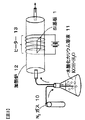
- FIG. 3 schematically shows a method for forming the SiO 2 film 2 containing K + ions. This method uses a so-called wet oxidation method for forming a SiO 2 film on a Si substrate.
- K + ions have been described as examples. However, by using an aqueous solution in which an appropriate substance is dissolved in pure water, other alkali ions, that is, cations of alkali metal elements or alkaline earth metal elements are used. Similarly, ions can be contained in the SiO 2 film.
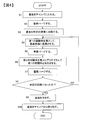
- FIG. 4 is a flowchart for explaining the process of the ALD method of the present embodiment.
- the ALD method of the present embodiment is called a plasma activated ALD method, and a first precursor (precursor) is adsorbed on the surface of an object to be deposited, and the second precursor is converted into plasma to form a first precursor. It is the method of making it deposit by making it react.
- step S1 a Si substrate (hereinafter referred to as a substrate) shown in FIG. 2A is placed in a chamber of a vacuum processing apparatus.
- step S2 the inside of the chamber is purged with nitrogen.
- step S3 the substrate is heated to a predetermined temperature.
- a predetermined temperature In this embodiment, it is set to 300 degrees.
- the plasma activated ALD method which is the ALD method of this embodiment, can be formed at room temperature.
- step S4 trimethylaluminum (TMA: Al (CH 3 ) 3 ), which is the first precursor, is introduced into the chamber, and trimethylaluminum is adsorbed on the surface of the substrate. After the adsorption, the inside of the chamber is purged with nitrogen in step S5. At that time, excess trimethylaluminum that has not been adsorbed on the surface of the substrate is discharged out of the chamber.
- TMA trimethylaluminum
- step S6 oxygen as the second precursor is introduced into the chamber. Then, the oxygen is converted into plasma at an output of 300 W and reacted with trimethylaluminum adsorbed on the surface of the substrate. As a result, aluminum oxide is formed on the substrate surface. Thereafter, in step S7, the inside of the chamber is purged with nitrogen, and reaction by-products are discharged out of the chamber.
- steps from S4 to S7 are defined as one cycle. Since the thickness of one cycle of the trimethylaluminum layer adsorbed on the substrate surface in step S4 is the thickness of one molecule of trimethylaluminum, only one atomic layer is formed in the aluminum oxide formed in step S6. It will be.
- step S8 it is determined whether the above cycle has been performed a predetermined number of times. If a negative determination is made, the process proceeds to step S4, and if a positive determination is made, the process proceeds to step S9. That is, the above cycle including steps S4 to S7 is repeated a predetermined number of times.
- the thickness of the deposit per cycle was determined as 1.09 [1.0 / cycle] from the thickness of 21.75 nm when 200 cycles were performed. Based on the thickness of the deposit per cycle, 184 cycles (predetermined number of times) of deposition were performed to form a 20 nm aluminum oxide film 5 on the surface of the electret device of this embodiment (FIG. 5). reference).
- the substrate is cooled and removed from the chamber in step S9.
- FIG. 5 shows a table of data relating to the aluminum oxide film 5 provided on the surface of the electret device of the present embodiment.
- an aluminum oxide film 5 of 20.43 nm having a substantially desired thickness could be obtained.
- L1 and L2 which are lengths in the thickness direction of the side walls of the comb electrode are about 20 ⁇ m.
- the gap G between the comb electrodes is about 1 ⁇ m.
- the aluminum oxide film formed by the ALD method of the present embodiment exhibits uniform film formability even on the surface having a high aspect ratio structure in which the lengths L1 and L2 are long with respect to the gap G.
- the charge stability of the electret element 20 can be improved as described later (see FIG. 7).
- FIG. 6A is a diagram for explaining a polarization method of the movable electrode 21 and the fixed electrode 22 of the electret element 20.
- FIG. 6B schematically shows a cross section near the surfaces of the comb-tooth electrode 211 of the movable electrode 21 and the comb-tooth electrode 221 of the fixed electrode 22 in the electret element 20.
- the polarization of the movable electrode 21 and the fixed electrode 22 of the electret element 20 is performed using the Bias-Temperature method (BT method) described in JP2013-13256A.
- BT method Bias-Temperature method
- the movable electrode 21 is connected to the negative electrode side of the DC power supply 30
- the fixed electrode 22 is connected to the positive electrode side of the DC power supply 30
- the movable electrode 21 and the fixed electrode 22 are heated to 630 ° C.
- polarization is performed by applying a DC voltage between the movable electrode 21 and the fixed electrode 22.
- the comb-teeth electrodes 211, K + ions contained in the SiO 2 film 2 the SiO 2 film 2 leftward direction, i.e., moves to the Si substrate 1 side.
- the comb electrodes 221, K + ions contained in the SiO 2 film 2 illustrates the SiO 2 film 2 left, i.e., moves to the aluminum oxide film 5 side.
- comb electrodes 211 and 221 After the movement in the SiO 2 film within the above second K + ions, the temperature remains movable electrode 21 and fixed electrode 22 by applying a DC voltage by the ambient temperature, K + ions The SiO 2 film 2 in the comb-tooth electrodes 211 and 221 is fixed to the moved position in the SiO 2 film 2 and is electretized. Thereafter, the application of the DC voltage is terminated.
- the vicinity of the surface of the comb electrode 211 is negatively charged, and the vicinity of the surface of the comb electrode 221 is positively charged.
- the electret device of the present embodiment has the following configuration and exhibits the following operational effects.
- a film 2 containing silicon oxide (SiO 2 ) is formed, and an aluminum oxide protective film 5 deposited by an atomic layer deposition method (ALD method) is formed on the film 2 Is done.
- ALD method atomic layer deposition method
- the film 2 is formed in a state containing K + ions and is electretized by being heated and applied with a voltage. Thereby, compared with the electret film
- the electret film 2 is formed on the side walls 212 and 222 of the comb electrodes 211 and 221.
- the aluminum oxide film 5 as a protective film is formed on the electret film 2 formed on the side walls 212 and 222.
- the moisture resistance of the side walls 212 and 222 of the comb-tooth electrodes 211 and 221 that have a high aspect ratio that makes it difficult to form a protective film can be improved, and the electret element 20 has good charge stability. Can contribute to sex.
- the protective film can be formed on the side walls 212 and 222 of the comb electrodes 211 and 221 which are difficult to form by using the ALD method.
- FIG. 7 shows the charge stability of the electret element (hereinafter referred to as an ALD product) of this embodiment in which a protective film for the aluminum oxide film 5 is provided on the surface, and the surface as described in Patent Document 2 and the like. It is the figure which compared the charge stability of the processed electret element (henceforth an HMDS product). As shown in FIG. 7, in the HMDS product, it can be seen that the charge cannot be retained after about 10 hours. On the other hand, in the ALD product, the electric charge is retained even after 10 hours. Thus, it is understood that the electret element 20 having the aluminum oxide film 5 of the present embodiment has good charge stability.
- FIG. 8 is a schematic diagram showing an example in which the electret element 20 is mounted on the condenser microphone 50 (condenser microphone 50) as an electrostatic induction electromechanical conversion element.
- the capacitor microphone 50 includes a diaphragm 51, a back plate 52, an insulating support member 53 that connects the diaphragm 51 and the back plate 52, and the electret element 20.
- the electret element 20 includes a movable electrode 21, a fixed electrode 22, an output terminal 23 of the movable electrode 21, and an output terminal 24 of the fixed electrode 22.
- the movable electrode 21 is provided on the diaphragm 51.
- the fixed electrode 22 is provided on the back plate 52.
- the movable electrode 21 and the fixed electrode 22 have electret films having different polarities, an electric field is generated between the movable electrode 21 and the fixed electrode 22.
- the movable electrode 21 vibrates as the diaphragm 51 is vibrated by receiving a wave such as sound, and the relative position with respect to the fixed electrode 22 changes.
- the voltage between the output terminal 23 and the output terminal 24 changes.
- a wave such as a sound that vibrates the diaphragm 51.
- a silicon oxide film containing alkali ions is formed using a wet oxidation method, and an aluminum oxide film manufactured by the ALD method is provided thereon as a protective film, and the Bias-Temperature method (BT). Method), the silicon oxide film is electretized to obtain an electret element.
- the present invention is not limited to this.
- the protective film made of an aluminum oxide film produced by the ALD method of this embodiment can be applied to a silicon oxide film electretized by corona discharge.
- the present invention is not limited to the contents described above.
- Other embodiments conceivable within the scope of the technical idea of the present invention are also included in the scope of the present invention.
- the present invention can also be applied to the surface of a complicated structure such as the element.
- the present invention can be applied to a simple element such as a flat element.
- Si substrate 2 SiO 2 film (electret film) 5: Aluminum oxide film (protective film) 20: electret element 21: movable electrode 22: fixed electrode 23, 24: output terminal 25: output resistance 50: condenser microphone (condenser microphone) 51: Diaphragm 52: Back plate 53: Support member 211: Comb electrode 212: Side wall 221: Comb electrode 222: Side wall G: Distance L1, L2: Length
Landscapes
- Engineering & Computer Science (AREA)
- Power Engineering (AREA)
- Chemical & Material Sciences (AREA)
- Physics & Mathematics (AREA)
- Acoustics & Sound (AREA)
- Signal Processing (AREA)
- Microelectronics & Electronic Packaging (AREA)
- Manufacturing & Machinery (AREA)
- Materials Engineering (AREA)
- Organic Chemistry (AREA)
- Inorganic Chemistry (AREA)
- Electrostatic, Electromagnetic, Magneto- Strictive, And Variable-Resistance Transducers (AREA)
Abstract
エレクトレット素子は、酸化シリコンを含むエレクトレット膜と、エレクトレット膜の上に形成された、原子層堆積法で堆積させた酸化アルミニウムの保護膜とを有する。
Description
本発明は、エレクトレット素子、当該エレクトレット素子を搭載したマイクロフォン、及び、当該エレクトレット素子の製造方法に関する。
コンデンサマイクなどには、振動エネルギーを電気エネルギーに変換する変換素子が設けられている。その変換素子には、エレクトレット、すなわち、誘電体に電圧を印加するなどして帯電を維持させた部材が用いられることがある。以下では、エレクトレットが用いられている素子を、エレクトレット素子と呼ぶ。
エレクトレットは、絶縁膜にコロナ放電で電荷を注入する方法、または、特許文献1に記載の方法などによって作製されている。
エレクトレットの帯電量は、時間が経つに連れ、低下していく。これを帯電劣化という。また、帯電劣化しにくい性質を、電荷安定性という。帯電劣化は、主に、エレクトレットが外気中の水分(湿気)と触れることによって生じる。
特許文献2には、エレクトレット構造にヘキサメチルジシラザンによる表面処理(HMDS処理)によって、撥水処理を施し、電荷安定性を向上させる発明が開示されている。しかし、当該発明は、表面に極めて薄い有機物質膜を形成したものなので、電荷安定性に疑問がある。
ところで、近年、MEMS(Micro Electro Mechanical Systems)の技術を利用し、櫛歯電極を立体的な構造とすることで、対向する電極間の静電容量を増加させた、小型の変換素子が作製されている。例えば特許文献3に開示されている変換素子では、このような立体的な対向する櫛歯電極が用いられており、電極間の電圧印加手段として、櫛歯電極の付近に設けたエレクトレットが用いられている。
上述のエレクトレットが用いられた立体的な櫛歯電極を有する変換素子においては、対向する電極間の間隔と櫛歯の厚み寸法とのアスペクト比が高い。当該アスペクト比が高い変換素子においては、HMDS処理が有効に働かず、良好な電荷安定性が得られないという問題がある。
このように、平板などの単純な構造だけでなく、アスペクト比が高い櫛歯構造を有するエレクトレット素子においても、良好な電荷安定性が得られるものが求められていた。
本発明の第1の態様によると、エレクトレット素子は、酸化シリコンを含むエレクトレット膜と、エレクトレット膜の上に形成された、原子層堆積法で堆積させた酸化アルミニウムの保護膜とを有する。
本発明の第2の態様によると、第1の態様のエレクトレット素子において、エレクトレット膜は、アルカリイオンを含み、加熱されて電圧を印加されて得られることが好ましい。
本発明の第3の態様によると、第1または2の態様のエレクトレット素子において、エレクトレット膜が形成された側壁を有する櫛歯を有する電極を備え、保護膜は、側壁に形成されていることが好ましい。
本発明の第4の態様によると、第3の態様のエレクトレット素子において、電極は、櫛歯として第1櫛歯が設けられた第1電極と、櫛歯として第2櫛歯が設けられた第2電極と、を含み、第1櫛歯は、側壁として、第1側壁を有し、第2櫛歯は、側壁として、第2側壁を有し、第1櫛歯と第2櫛歯とは、第1側壁と第2側壁とが所定の間隔をもって互いに対向するように、歯合されていることが好ましい。
本発明の第5の態様によると、マイクロフォンは、第4の態様のエレクトレット素子を静電誘導型電気機械変換素子として備える。
本発明の第6の態様によると、エレクトレット素子の製造方法は、基板の上に、アルカリイオンを含んだシリコン酸化膜を形成し、シリコン酸化膜の上に、原子層堆積法で酸化アルミニウムを堆積させ、基板を加熱し電圧を印加してアルカリイオンを移動させることで、電気分極させる。
本発明の第7の態様によると、第6の態様のエレクトレット素子の製造方法において、基板は、第1櫛歯と、第2櫛歯と、を有し、電気分極は、基板を加熱して、第1櫛歯と第2櫛歯との間に電圧を印加して、アルカリイオンを移動させて行われる、ことが好ましい。
本発明の第2の態様によると、第1の態様のエレクトレット素子において、エレクトレット膜は、アルカリイオンを含み、加熱されて電圧を印加されて得られることが好ましい。
本発明の第3の態様によると、第1または2の態様のエレクトレット素子において、エレクトレット膜が形成された側壁を有する櫛歯を有する電極を備え、保護膜は、側壁に形成されていることが好ましい。
本発明の第4の態様によると、第3の態様のエレクトレット素子において、電極は、櫛歯として第1櫛歯が設けられた第1電極と、櫛歯として第2櫛歯が設けられた第2電極と、を含み、第1櫛歯は、側壁として、第1側壁を有し、第2櫛歯は、側壁として、第2側壁を有し、第1櫛歯と第2櫛歯とは、第1側壁と第2側壁とが所定の間隔をもって互いに対向するように、歯合されていることが好ましい。
本発明の第5の態様によると、マイクロフォンは、第4の態様のエレクトレット素子を静電誘導型電気機械変換素子として備える。
本発明の第6の態様によると、エレクトレット素子の製造方法は、基板の上に、アルカリイオンを含んだシリコン酸化膜を形成し、シリコン酸化膜の上に、原子層堆積法で酸化アルミニウムを堆積させ、基板を加熱し電圧を印加してアルカリイオンを移動させることで、電気分極させる。
本発明の第7の態様によると、第6の態様のエレクトレット素子の製造方法において、基板は、第1櫛歯と、第2櫛歯と、を有し、電気分極は、基板を加熱して、第1櫛歯と第2櫛歯との間に電圧を印加して、アルカリイオンを移動させて行われる、ことが好ましい。
本発明によれば、良好な成膜性を示し、良好な耐湿性を示し、良好な電荷安定性を有するエレクトレット素子を提供できる。本発明は、平板などの単純な構造だけでなく、対向する電極間の間隔と櫛歯の厚み寸法とのアスペクト比が高い櫛歯構造を有するエレクトレット素子においても、有効に働く。また、そのエレクトレット素子をマイクロフォンに搭載すれば、良好な電荷安定性を有するマイクロフォンを提供できる。
本明細書では、誘電体に電圧を印加するなどして帯電を維持させた部材をエレクトレットと呼ぶ。誘電体に電圧を印加するなどして帯電を維持させることをエレクトレット化と呼ぶ。エレクトレットの膜をエレクトレット膜と呼ぶ。エレクトレットが用いられている素子をエレクトレット素子と呼ぶ。また、本明細書では、アルカリ金属元素の陽イオンやアルカリ土類金属元素の陽イオンを総称して、アルカリイオンと呼ぶ。
―エレクトレット素子の実施形態―
図1(a)は、エレクトレット素子20(振動素子20)の構造を簡略化して示したものである。図1(b)は、後述する櫛歯電極211、221の周辺の拡大図である。
図1(a)は、エレクトレット素子20(振動素子20)の構造を簡略化して示したものである。図1(b)は、後述する櫛歯電極211、221の周辺の拡大図である。
図1(a)に示すように、エレクトレット素子20は、可動電極21と固定電極22とを備える。可動電極21には、立体型の櫛歯電極211が複数設けられている。固定電極22には、立体型の櫛歯電極221が複数設けられている。櫛歯電極211、221の数はエレクトレット素子20の出力の仕様に対応して適宜増減して作製される。
図1(b)に示すように、櫛歯電極211は、厚み方向の長さがL1である側壁212を有する。櫛歯電極221は、厚み方向の長さがL2である側壁222を有する。櫛歯電極211と櫛歯電極221は、所定の間隔Gを空け、側壁212、222を対向させて互いに歯合している。なお、本実施形態では、長さL1、L2はそれぞれ20μm程度であり、間隔Gは、1μm程度である。
可動電極21及び固定電極22の表面(側壁212,222含む)には、後述するK+イオンを含むSiO2膜であるエレクトレット膜が形成されている。当該エレクトレット膜の上には、後述するALD法によって酸化アルミニウム膜が形成されている。当該酸化アルミニウム膜は、耐湿性を高めて電荷安定性を高める保護膜として設けられている。
図1(a)において、可動電極21は、バネ性を有する不図示の支持体で支持され、外部からの振動によって振動する。当該支持体は、可動電極21と固定電極22が製造される製造プロセスで一緒に製造される。
可動電極21が振動すると、櫛歯電極211と櫛歯電極221との相対的な位置関係が変化して、出力端子23と出力端子24の間に出力電圧が出力される。なお、出力を電流として利用する場合は、例えば出力抵抗25の代わりに、整流回路を接続し、さらに整流後のDC電流を蓄えるコンデンサを用いる。
図2は、エレクトレット素子20を作成するに際し行う成膜について説明した図である。図2(a)に示すように、Si基板1の上に、K+イオンを含有するSiO2膜2を形成する。このSiO2膜2の形成方法については後述する。このSiO2膜2が含有するK+イオンは、常温においてはSiO2膜2内を移動することはできない。
次に、図2(b)に示すように、SiO2膜2の上に、原子層堆積法(ALD法:Atomic Layer Deposition)によって、酸化アルミニウム膜(Al2O3)5を形成する。この酸化アルミニウム膜5は、耐湿性を高め、電荷安定性を高めるための保護膜として設けられている。なお、ALD法による酸化アルミニウム膜5の形成については、後述する。
図3は、K+イオンを含有するSiO2膜2の形成方法を模式的に示したものである。当該方法は、いわゆるウェット酸化方法と呼ばれる、Si基板にSiO2膜を形成する方法を利用している。
純水にKOHを溶解した水溶液にN2ガスを通過させ、このN2ガスにK+イオンを含んだ水蒸気を含有させる。このN2ガスを加熱炉12内に流しながら、加熱炉12内に設置されたエレクトレット素子の基板であるSi基板1を加熱すると、Si基板1の表面にK+イオンを含有したSiO2膜2が形成される。
以上では、K+イオンを例に説明したが、適当な物質を純水に溶解させた水溶液を用いることにより、その他のアルカリイオン、すなわち、アルカリ金属元素の陽イオンやアルカリ土類金属元素の陽イオンでも、同様にSiO2膜に含有させることができる。
図4は、本実施形態のALD法の工程を説明するためのフローチャートである。
本実施形態のALD法は、プラズマ活性化ALD法と呼ばれるもので、第1の前駆体(プリカーサー)を被堆積物の表面に吸着させ、第2の前駆体をプラズマ化して第1の前駆体と反応させることで堆積させる方法である。
図4を用いて、酸化アルミニウム膜5の作製方法について説明する。
ステップS1において、図2(a)に示すSi基板(以下、基板と呼ぶ)を真空処理装置のチャンバに入れる。ステップS2において、チャンバ内を窒素パージする。
ステップS1において、図2(a)に示すSi基板(以下、基板と呼ぶ)を真空処理装置のチャンバに入れる。ステップS2において、チャンバ内を窒素パージする。
ステップS3において、基板を所定の温度に熱する。本実施形態では、300度に設定している。なお、本実施形態のALD法であるプラズマ活性化ALD法は、常温でも成膜可能である。
ステップS4において、第1の前駆体であるトリメチルアルミニウム(TMA:Al(CH3)3)をチャンバ内に導入して、基板の表面にトリメチルアルミニウムを吸着させる。当該吸着後、ステップS5において、チャンバ内を窒素パージする。その際、基板の表面に吸着しなかった余分なトリメチルアルミニウムはチャンバ外に排出される。
ステップS6において、第2の前駆体である酸素をチャンバ内に導入する。そして、その酸素を300Wの出力でプラズマ化し、基板の表面に吸着したトリメチルアルミニウムと反応させる。その結果、基板表面には、酸化アルミニウムが形成される。その後、ステップS7において、チャンバ内を窒素パージして、反応副生成物をチャンバ外に排出する。
これらステップS4~S7までのステップを1サイクルとする。なお、ステップS4において基板表面に吸着されるトリメチルアルミニウム層の1サイクル分の厚みは、トリメチルアルミニウムの1分子の厚みであるため、ステップS6によって形成される酸化アルミニウムは、1原子層だけ形成されることになる。
ステップS8において、上記のサイクルを所定の回数行ったかを判定する。否定判定されればステップS4に移行し、肯定判定されればステップS9に移行する。すなわち、所定の回数だけ、ステップS4~S7を含む上記のサイクルを繰り返す。なお、サイクルの回収基準ではなく、酸化アルミニウム膜5の厚み基準で成膜する場合は、1サイクル当たりの堆積物の厚みを事前に予備実験をして調べておく必要がある。図示していないが、本実施形態では、事前に予備実験を行い、200サイクル行った時の厚み21.75nmから1サイクル当たりの堆積物の厚みを1.09[Å/サイクル]として求めた。その1サイクル当たりの堆積物の厚みをもとにして、本実施形態のエレクトレット素子の表面に、20nmの酸化アルミニウム膜5を形成すべく、184サイクル(所定の回数)堆積を行った(図5参照)。
所定の回数だけサイクルを繰り返して堆積させたら、ステップS9において基板を冷まし、チャンバから取り出す。
図5に、本実施形態のエレクトレット素子の表面に設けた酸化アルミニウム膜5に関するデータの表を示す。上記の予備実験によって、ほぼ所望の厚みである20.43nmの酸化アルミニウム膜5を得ることができた。
上述のように、櫛歯電極の側壁の厚み方向の長さであるL1、L2は、20μm程度である。一方、櫛歯電極の間隔Gは、1μm程度である。このように、間隔Gに対して、長さL1、L2が長い高アスペクト比の構造の表面に対しても、本実施形態のALD法による酸化アルミニウム膜は、均一な成膜性を示す。その結果、良好な耐湿性を示すため、後述するように、エレクトレット素子20の電荷安定性を向上させることができる(図7参照)。
図6(a)は、エレクトレット素子20の可動電極21、固定電極22の分極方法について説明するための図である。図6(b)は、エレクトレット素子20における可動電極21の櫛歯電極211および固定電極22の櫛歯電極221の表面付近の断面を概略的に示したものである。
本実施形態では、エレクトレット素子20の可動電極21、固定電極22の分極を、特開2013-13256号公報に記載のBias-Temperature法(B-T法)を用いて行う。図6(a)に示すように、可動電極21を直流電源30の負極側に接続し、固定電極22を直流電源30の正極側に接続し、可動電極21及び固定電極22を630℃に加熱した状態で、可動電極21と固定電極22との間に直流電圧を印加することで分極させる。この分極の工程で、櫛歯電極211においては、SiO2膜2に含有されるK+イオンが、SiO2膜2内を図示左方向、すなわち、Si基板1側に移動する。一方、櫛歯電極221においては、SiO2膜2に含有されるK+イオンが、SiO2膜2内を図示左方向、すなわち、酸化アルミニウム膜5側に移動する。櫛歯電極211、221において、上記のK+イオンのSiO2膜2内での移動後、直流電圧を印加したまま可動電極21及び固定電極22の温度を常温にすることで、K+イオンがSiO2膜2内の移動した位置に固定され、櫛歯電極211、221におけるSiO2膜2がそれぞれエレクトレット化される。その後、直流電圧の印加を終了する。以上の工程を経ることで、図6(b)に示すように、櫛歯電極211の表面近傍はマイナスに帯電され、櫛歯電極221の表面近傍はプラスに帯電される。
本実施形態のエレクトレット素子は、以下の構成を備え、以下の作用効果を奏する。
(1)エレクトレット素子20においては、酸化シリコン(SiO2)を含む膜2が形成され、膜2の上には、原子層堆積法(ALD法)で堆積させた酸化アルミニウムの保護膜5が形成される。
これによって、耐湿性を向上させ、帯電劣化を抑制し、良好な電荷安定性を有するエレクトレット素子を得ることができる。
(1)エレクトレット素子20においては、酸化シリコン(SiO2)を含む膜2が形成され、膜2の上には、原子層堆積法(ALD法)で堆積させた酸化アルミニウムの保護膜5が形成される。
これによって、耐湿性を向上させ、帯電劣化を抑制し、良好な電荷安定性を有するエレクトレット素子を得ることができる。
(2)膜2は、K+イオンを含んだ状態で形成され、加熱されて電圧を印加されることにより、エレクトレット化される。
これによって、コロナ放電によって作製されたエレクトレット膜と比較して、良好な電荷安定性を有する。
これによって、コロナ放電によって作製されたエレクトレット膜と比較して、良好な電荷安定性を有する。
(3)櫛歯電極211,221の側壁212,222には、エレクトレット膜2が形成されている。保護膜である酸化アルミニウム膜5は、側壁212,222に形成されたエレクトレット膜2の上に、形成されている。
これによって、櫛歯電極211,221の側壁212,222という、保護膜を成膜しにくいような高アスペクト比を有する部分における耐湿性をも向上させることができ、エレクトレット素子20の良好な電荷安定性に貢献できる。
なお、櫛歯電極211,221の側壁212,222という、成膜しにくい部分への保護膜の成膜は、ALD法を用いたことによって可能となった。
これによって、櫛歯電極211,221の側壁212,222という、保護膜を成膜しにくいような高アスペクト比を有する部分における耐湿性をも向上させることができ、エレクトレット素子20の良好な電荷安定性に貢献できる。
なお、櫛歯電極211,221の側壁212,222という、成膜しにくい部分への保護膜の成膜は、ALD法を用いたことによって可能となった。
図7は、酸化アルミニウム膜5の保護膜を表面に設けた本実施形態のエレクトレット素子(以下、ALD品と呼ぶ)の電荷安定性と、特許文献2等に記載されているような表面をHMDS処理したエレクトレット素子(以下、HMDS品と呼ぶ)の電荷安定性とを比較した図である。図7に示すように、HMDS品においては、10時間を過ぎたあたりから電荷が保持できなくなっているのが分かる。一方、ALD品においては、10時間を過ぎた後も電荷が保持されている。このように、本実施形態の酸化アルミニウム膜5が形成されたエレクトレット素子20の電荷安定性が良好であることが理解される。
―マイクロフォンの実施形態―
図8は、コンデンサマイクロフォン50(コンデンサマイク50)に、エレクトレット素子20を静電誘導型電気機械変換素子として搭載した一例を示した模式図である。コンデンサマイク50は、ダイアフラム51と、バックプレート52と、ダイアフラム51とバックプレート52とを接続する絶縁性の支持部材53と、エレクトレット素子20と、を備えている。
図8は、コンデンサマイクロフォン50(コンデンサマイク50)に、エレクトレット素子20を静電誘導型電気機械変換素子として搭載した一例を示した模式図である。コンデンサマイク50は、ダイアフラム51と、バックプレート52と、ダイアフラム51とバックプレート52とを接続する絶縁性の支持部材53と、エレクトレット素子20と、を備えている。
エレクトレット素子20は、可動電極21と、固定電極22と、可動電極21の出力端子23と、固定電極22の出力端子24と、を備えている。可動電極21は、ダイアフラム51に設けられている。固定電極22は、バックプレート52に設けられている。
可動電極21と固定電極22は、互いに極性の異なるエレクトレット膜を有しているため、可動電極21と固定電極22との間には電界が生じている。ダイアフラム51が音などの波動を受けて振動することに伴って可動電極21が振動し、固定電極22との相対位置が変化する。これによって、出力端子23と出力端子24との間の電圧が変化する。この電圧変化を検出することで、ダイアフラム51を振動させた音などの波動を推定することができる。
次のような変形も本発明の範囲内である。
以上の実施形態では、ウェット酸化方法を用いてアルカリイオンを含むシリコン酸化膜を形成し、その上に、保護膜としてALD法で作製された酸化アルミニウム膜を設け、Bias-Temperature法(B-T法)により、シリコン酸化膜をエレクトレット化して、エレクトレット素子を得るとしたが、これに限定されない。本実施形態のALD法で作製された酸化アルミニウム膜で作製された保護膜は、コロナ放電によってエレクトレット化されたシリコン酸化膜などにも適用可能である。
本発明は、以上に示した内容に限定されるものではない。本発明の技術的思想の範囲内で考えられるその他の態様も本発明の範囲内に含まれる。例えば、以上の実施形態では櫛歯電極を有する素子の表面にALD法による保護膜を設ける例を示したが、当該素子のような複雑な構造の表面にも本発明は適用できるのであるから、平板状の素子のような単純な形状の素子においても、当然ながら、本発明は適用できる。
次の優先権基礎出願の開示内容は引用文としてここに組み込まれる。
日本国特許出願2014年第215229号(2014年10月22日出願)
日本国特許出願2014年第215229号(2014年10月22日出願)
1:Si基板
2:SiO2膜(エレクトレット膜)
5:酸化アルミニウム膜(保護膜)
20:エレクトレット素子
21:可動電極
22:固定電極
23、24:出力端子
25:出力抵抗
50:コンデンサマイクロフォン(コンデンサマイク)
51:ダイアフラム
52:バックプレート
53:支持部材
211:櫛歯電極
212:側壁
221:櫛歯電極
222:側壁
G:間隔
L1、L2:長さ
2:SiO2膜(エレクトレット膜)
5:酸化アルミニウム膜(保護膜)
20:エレクトレット素子
21:可動電極
22:固定電極
23、24:出力端子
25:出力抵抗
50:コンデンサマイクロフォン(コンデンサマイク)
51:ダイアフラム
52:バックプレート
53:支持部材
211:櫛歯電極
212:側壁
221:櫛歯電極
222:側壁
G:間隔
L1、L2:長さ
Claims (7)
- 酸化シリコンを含むエレクトレット膜と、
前記エレクトレット膜の上に形成された、原子層堆積法で堆積させた酸化アルミニウムの保護膜とを有するエレクトレット素子。 - 請求項1に記載のエレクトレット素子において、
前記エレクトレット膜は、アルカリイオンを含み、
加熱されて電圧を印加されて得られるエレクトレット素子。 - 請求項1または2に記載のエレクトレット素子において、
前記エレクトレット膜が形成された側壁を有する櫛歯を有する電極を備え、
前記保護膜は、前記側壁に形成されているエレクトレット素子。 - 請求項3に記載のエレクトレット素子において、
前記電極は、前記櫛歯として第1櫛歯が設けられた第1電極と、前記櫛歯として第2櫛歯が設けられた第2電極と、を含み、
前記第1櫛歯は、前記側壁として、第1側壁を有し、
前記第2櫛歯は、前記側壁として、第2側壁を有し、
前記第1櫛歯と前記第2櫛歯とは、前記第1側壁と前記第2側壁とが所定の間隔をもって互いに対向するように、歯合されているエレクトレット素子。 - 請求項4に記載のエレクトレット素子を静電誘導型電気機械変換素子として備えるマイクロフォン。
- 基板の上に、アルカリイオンを含んだシリコン酸化膜を形成し、
前記シリコン酸化膜の上に、原子層堆積法で酸化アルミニウムを堆積させ、
前記基板を加熱し電圧を印加して前記アルカリイオンを移動させることで、電気分極させるエレクトレット素子の製造方法。 - 請求項6に記載のエレクトレット素子の製造方法において、
前記基板は、第1櫛歯と、第2櫛歯と、を有し、
前記電気分極は、前記基板を加熱して、前記第1櫛歯と前記第2櫛歯との間に電圧を印加して、前記アルカリイオンを移動させて行われる、エレクトレット素子の製造方法。
Priority Applications (3)
| Application Number | Priority Date | Filing Date | Title |
|---|---|---|---|
| US15/520,549 US10511914B2 (en) | 2014-10-22 | 2015-10-14 | Electret element, microphone having electret element mounted therein and electret element manufacturing method |
| CN201580057825.XA CN107112136B (zh) | 2014-10-22 | 2015-10-14 | 驻极体元件、搭载该驻极体元件的话筒以及该驻极体元件的制造方法 |
| US16/129,836 US10405103B2 (en) | 2014-10-22 | 2018-09-13 | Electret element, microphone having electret element mounted therein and electret element manufacturing method |
Applications Claiming Priority (2)
| Application Number | Priority Date | Filing Date | Title |
|---|---|---|---|
| JP2014215229A JP6554742B2 (ja) | 2014-10-22 | 2014-10-22 | エレクトレット素子、当該エレクトレット素子を搭載したマイクロフォン、及び、当該エレクトレット素子の製造方法 |
| JP2014-215229 | 2014-10-22 |
Related Child Applications (2)
| Application Number | Title | Priority Date | Filing Date |
|---|---|---|---|
| US15/520,549 A-371-Of-International US10511914B2 (en) | 2014-10-22 | 2015-10-14 | Electret element, microphone having electret element mounted therein and electret element manufacturing method |
| US16/129,836 Division US10405103B2 (en) | 2014-10-22 | 2018-09-13 | Electret element, microphone having electret element mounted therein and electret element manufacturing method |
Publications (1)
| Publication Number | Publication Date |
|---|---|
| WO2016063767A1 true WO2016063767A1 (ja) | 2016-04-28 |
Family
ID=55760810
Family Applications (1)
| Application Number | Title | Priority Date | Filing Date |
|---|---|---|---|
| PCT/JP2015/079018 Ceased WO2016063767A1 (ja) | 2014-10-22 | 2015-10-14 | エレクトレット素子、当該エレクトレット素子を搭載したマイクロフォン、及び、当該エレクトレット素子の製造方法 |
Country Status (4)
| Country | Link |
|---|---|
| US (2) | US10511914B2 (ja) |
| JP (1) | JP6554742B2 (ja) |
| CN (1) | CN107112136B (ja) |
| WO (1) | WO2016063767A1 (ja) |
Families Citing this family (9)
| Publication number | Priority date | Publication date | Assignee | Title |
|---|---|---|---|---|
| JP2018088780A (ja) * | 2016-11-29 | 2018-06-07 | 国立大学法人 東京大学 | 振動発電素子 |
| JP2019033631A (ja) * | 2017-08-09 | 2019-02-28 | 国立大学法人静岡大学 | Mems振動素子、mems振動素子の製造方法および振動発電素子 |
| JP7037144B2 (ja) * | 2017-08-09 | 2022-03-16 | 国立大学法人静岡大学 | Mems振動素子の製造方法およびmems振動素子 |
| JP7410935B2 (ja) | 2018-05-24 | 2024-01-10 | ザ リサーチ ファウンデーション フォー ザ ステイト ユニバーシティー オブ ニューヨーク | 容量性センサ |
| JP6927530B2 (ja) * | 2018-11-16 | 2021-09-01 | 国立大学法人 東京大学 | 櫛歯型素子の製造方法 |
| JP7075593B2 (ja) * | 2018-11-16 | 2022-05-26 | 国立大学法人 東京大学 | 振動発電素子 |
| JP7090249B2 (ja) * | 2019-06-06 | 2022-06-24 | 国立大学法人 東京大学 | 静電型デバイスを製造する製造方法 |
| WO2021134679A1 (zh) * | 2019-12-31 | 2021-07-08 | 瑞声声学科技(深圳)有限公司 | 电容系统及电容式麦克风 |
| US12151933B2 (en) * | 2021-03-16 | 2024-11-26 | Aac Acoustic Technologies (Shenzhen) Co., Ltd. | Comb-drive device used in micro electro mechanical system |
Citations (3)
| Publication number | Priority date | Publication date | Assignee | Title |
|---|---|---|---|---|
| JP2009164539A (ja) * | 2008-01-10 | 2009-07-23 | Nippon Hoso Kyokai <Nhk> | エレクトレット構造及びその形成方法並びにエレクトレット型静電容量センサ |
| JP2013235978A (ja) * | 2012-05-09 | 2013-11-21 | Panasonic Corp | 薄膜製造方法および表示パネルの製造方法、tft基板の製造方法 |
| JP2014050196A (ja) * | 2012-08-30 | 2014-03-17 | Aoi Electronics Co Ltd | 正イオンを含有したエレクトレットの形成方法 |
Family Cites Families (13)
| Publication number | Priority date | Publication date | Assignee | Title |
|---|---|---|---|---|
| CA1336295C (en) * | 1988-09-21 | 1995-07-11 | Masayoshi Miura | Sound reproducing apparatus |
| US7638252B2 (en) * | 2005-01-28 | 2009-12-29 | Hewlett-Packard Development Company, L.P. | Electrophotographic printing of electronic devices |
| TWI323617B (en) * | 2006-02-20 | 2010-04-11 | Cotron Corp | Multiple channel earphone |
| US7993959B2 (en) * | 2006-09-14 | 2011-08-09 | The Johns Hopkins University | Methods for producing multiple distinct transistors from a single semiconductor |
| CN101256900A (zh) * | 2006-09-29 | 2008-09-03 | 三洋电机株式会社 | 驻极体元件及具备该驻极体元件的静电感应型转换装置 |
| JP2008182666A (ja) | 2006-12-28 | 2008-08-07 | Matsushita Electric Ind Co Ltd | エレクトレットコンデンサマイク及びその製造方法 |
| US20080155801A1 (en) | 2006-12-28 | 2008-07-03 | Hirofumi Imanaka | Electret condenser microphone and manufacturing method thereof |
| JP5237705B2 (ja) * | 2008-06-24 | 2013-07-17 | パナソニック株式会社 | 発電デバイス |
| US8798298B1 (en) * | 2008-12-31 | 2014-08-05 | Starkey Laboratories, Inc. | Constrained layer damping for hearing assistance devices |
| JP5676377B2 (ja) * | 2011-06-29 | 2015-02-25 | アオイ電子株式会社 | エレクトレット膜およびこれを用いた振動発電素子 |
| JP5763023B2 (ja) * | 2012-08-30 | 2015-08-12 | アオイ電子株式会社 | 立体型櫛歯エレクトレット電極の製造方法 |
| JP2014107890A (ja) * | 2012-11-26 | 2014-06-09 | Panasonic Corp | エレクトレット素子およびそれを用いた振動発電器 |
| JP5855602B2 (ja) * | 2013-05-22 | 2016-02-09 | アオイ電子株式会社 | 静電誘導型電気機械変換素子およびナノピンセット |
-
2014
- 2014-10-22 JP JP2014215229A patent/JP6554742B2/ja active Active
-
2015
- 2015-10-14 US US15/520,549 patent/US10511914B2/en active Active
- 2015-10-14 WO PCT/JP2015/079018 patent/WO2016063767A1/ja not_active Ceased
- 2015-10-14 CN CN201580057825.XA patent/CN107112136B/zh active Active
-
2018
- 2018-09-13 US US16/129,836 patent/US10405103B2/en active Active
Patent Citations (3)
| Publication number | Priority date | Publication date | Assignee | Title |
|---|---|---|---|---|
| JP2009164539A (ja) * | 2008-01-10 | 2009-07-23 | Nippon Hoso Kyokai <Nhk> | エレクトレット構造及びその形成方法並びにエレクトレット型静電容量センサ |
| JP2013235978A (ja) * | 2012-05-09 | 2013-11-21 | Panasonic Corp | 薄膜製造方法および表示パネルの製造方法、tft基板の製造方法 |
| JP2014050196A (ja) * | 2012-08-30 | 2014-03-17 | Aoi Electronics Co Ltd | 正イオンを含有したエレクトレットの形成方法 |
Also Published As
| Publication number | Publication date |
|---|---|
| US10511914B2 (en) | 2019-12-17 |
| US10405103B2 (en) | 2019-09-03 |
| JP2016082836A (ja) | 2016-05-16 |
| US20170318394A1 (en) | 2017-11-02 |
| CN107112136B (zh) | 2019-10-08 |
| CN107112136A (zh) | 2017-08-29 |
| JP6554742B2 (ja) | 2019-08-07 |
| US20190014419A1 (en) | 2019-01-10 |
Similar Documents
| Publication | Publication Date | Title |
|---|---|---|
| JP6554742B2 (ja) | エレクトレット素子、当該エレクトレット素子を搭載したマイクロフォン、及び、当該エレクトレット素子の製造方法 | |
| JP5763023B2 (ja) | 立体型櫛歯エレクトレット電極の製造方法 | |
| JP6870200B2 (ja) | 素子、及び発電装置 | |
| JP6628255B2 (ja) | 酸化グラフェンベースの音響トランスデューサの方法及び装置 | |
| KR20180038855A (ko) | 마이크로폰 및 이의 제조 방법 | |
| CN102728534A (zh) | 机电换能器及其制造方法 | |
| WO2011021488A1 (ja) | 静電誘導型発電装置 | |
| JP5627130B2 (ja) | 正イオンを含有したエレクトレットの形成方法 | |
| TW201241900A (en) | Treatment of a self-assembled monolayer on a dielectric layer for improved epoxy adhesion | |
| CN104064670B (zh) | 压电薄膜元件、压电传感器和振动发电机 | |
| JP2016209935A (ja) | エレクトレットの形成方法、mems装置 | |
| KR20130033218A (ko) | 잉크젯 프린팅을 이용한 그래핀 전극 제조 방법 | |
| JP4795633B2 (ja) | 基材上に圧電性厚膜を製造する方法 | |
| CN114698372B (zh) | 声波换能单元及其制作方法、声波换能器 | |
| JP2013201346A (ja) | 圧電素子及び圧電素子の製造方法 | |
| KR20210050254A (ko) | 전도성 기판 및 이를 포함하는 열음파 확성기 | |
| KR101330713B1 (ko) | 레이저 리프트오프를 이용한 플렉서블 박막 나노제너레이터 제조방법 및 이에 의하여 제조된 플렉서블 박막 나노제너레이터 | |
| JP2009207344A (ja) | エレクトレット機械電気エネルギー変換装置およびその製造方法 | |
| JP2017099208A (ja) | エレクトレットおよびエレクトレットの製造方法 | |
| CN105197877B (zh) | 微机电封装结构及其制作方法 | |
| JP2019106883A (ja) | エレクトレット | |
| Kobayashi et al. | Pulse poling within 1 second enhance the piezoelectric property of PZT thin films | |
| JP5800710B2 (ja) | 圧電素子の製造方法 | |
| KR20260051556A (ko) | 이차원 압전 물질 기반의 마이크로폰 소자 및 이의 제조 방법 | |
| JP3187824U (ja) | 固体アルミニウム電解コンデンサの陰極炭素含有アルミニウム箔構造 |
Legal Events
| Date | Code | Title | Description |
|---|---|---|---|
| 121 | Ep: the epo has been informed by wipo that ep was designated in this application |
Ref document number: 15852453 Country of ref document: EP Kind code of ref document: A1 |
|
| WWE | Wipo information: entry into national phase |
Ref document number: 15520549 Country of ref document: US |
|
| NENP | Non-entry into the national phase |
Ref country code: DE |
|
| 122 | Ep: pct application non-entry in european phase |
Ref document number: 15852453 Country of ref document: EP Kind code of ref document: A1 |