WO2016063752A1 - 光電気混載基板およびその製法 - Google Patents
光電気混載基板およびその製法 Download PDFInfo
- Publication number
- WO2016063752A1 WO2016063752A1 PCT/JP2015/078820 JP2015078820W WO2016063752A1 WO 2016063752 A1 WO2016063752 A1 WO 2016063752A1 JP 2015078820 W JP2015078820 W JP 2015078820W WO 2016063752 A1 WO2016063752 A1 WO 2016063752A1
- Authority
- WO
- WIPO (PCT)
- Prior art keywords
- electric
- opto
- processing
- alignment mark
- electric hybrid
- Prior art date
- Legal status (The legal status is an assumption and is not a legal conclusion. Google has not performed a legal analysis and makes no representation as to the accuracy of the status listed.)
- Ceased
Links
Images





Classifications
-
- G—PHYSICS
- G02—OPTICS
- G02B—OPTICAL ELEMENTS, SYSTEMS OR APPARATUS
- G02B6/00—Light guides; Structural details of arrangements comprising light guides and other optical elements, e.g. couplings
- G02B6/24—Coupling light guides
- G02B6/42—Coupling light guides with opto-electronic elements
- G02B6/4201—Packages, e.g. shape, construction, internal or external details
- G02B6/4274—Electrical aspects
- G02B6/428—Electrical aspects containing printed circuit boards [PCB]
-
- G—PHYSICS
- G02—OPTICS
- G02B—OPTICAL ELEMENTS, SYSTEMS OR APPARATUS
- G02B6/00—Light guides; Structural details of arrangements comprising light guides and other optical elements, e.g. couplings
- G02B6/10—Light guides; Structural details of arrangements comprising light guides and other optical elements, e.g. couplings of the optical waveguide type
- G02B6/12—Light guides; Structural details of arrangements comprising light guides and other optical elements, e.g. couplings of the optical waveguide type of the integrated circuit kind
- G02B6/122—Basic optical elements, e.g. light-guiding paths
-
- G—PHYSICS
- G02—OPTICS
- G02B—OPTICAL ELEMENTS, SYSTEMS OR APPARATUS
- G02B6/00—Light guides; Structural details of arrangements comprising light guides and other optical elements, e.g. couplings
- G02B6/10—Light guides; Structural details of arrangements comprising light guides and other optical elements, e.g. couplings of the optical waveguide type
- G02B6/12—Light guides; Structural details of arrangements comprising light guides and other optical elements, e.g. couplings of the optical waveguide type of the integrated circuit kind
- G02B6/13—Integrated optical circuits characterised by the manufacturing method
-
- G—PHYSICS
- G02—OPTICS
- G02B—OPTICAL ELEMENTS, SYSTEMS OR APPARATUS
- G02B6/00—Light guides; Structural details of arrangements comprising light guides and other optical elements, e.g. couplings
- G02B6/24—Coupling light guides
- G02B6/42—Coupling light guides with opto-electronic elements
- G02B6/43—Arrangements comprising a plurality of opto-electronic elements and associated optical interconnections
-
- H—ELECTRICITY
- H05—ELECTRIC TECHNIQUES NOT OTHERWISE PROVIDED FOR
- H05K—PRINTED CIRCUITS; CASINGS OR CONSTRUCTIONAL DETAILS OF ELECTRIC APPARATUS; MANUFACTURE OF ASSEMBLAGES OF ELECTRICAL COMPONENTS
- H05K1/00—Printed circuits
- H05K1/02—Details
- H05K1/0266—Marks, test patterns or identification means
- H05K1/0269—Marks, test patterns or identification means for visual or optical inspection
-
- H—ELECTRICITY
- H05—ELECTRIC TECHNIQUES NOT OTHERWISE PROVIDED FOR
- H05K—PRINTED CIRCUITS; CASINGS OR CONSTRUCTIONAL DETAILS OF ELECTRIC APPARATUS; MANUFACTURE OF ASSEMBLAGES OF ELECTRICAL COMPONENTS
- H05K1/00—Printed circuits
- H05K1/02—Details
- H05K1/0274—Optical details, e.g. printed circuits comprising integral optical means
-
- H—ELECTRICITY
- H05—ELECTRIC TECHNIQUES NOT OTHERWISE PROVIDED FOR
- H05K—PRINTED CIRCUITS; CASINGS OR CONSTRUCTIONAL DETAILS OF ELECTRIC APPARATUS; MANUFACTURE OF ASSEMBLAGES OF ELECTRICAL COMPONENTS
- H05K1/00—Printed circuits
- H05K1/02—Details
- H05K1/03—Use of materials for the substrate
- H05K1/0313—Organic insulating material
- H05K1/032—Organic insulating material consisting of one material
- H05K1/0326—Organic insulating material consisting of one material containing O
-
- H—ELECTRICITY
- H05—ELECTRIC TECHNIQUES NOT OTHERWISE PROVIDED FOR
- H05K—PRINTED CIRCUITS; CASINGS OR CONSTRUCTIONAL DETAILS OF ELECTRIC APPARATUS; MANUFACTURE OF ASSEMBLAGES OF ELECTRICAL COMPONENTS
- H05K1/00—Printed circuits
- H05K1/02—Details
- H05K1/03—Use of materials for the substrate
- H05K1/0313—Organic insulating material
- H05K1/032—Organic insulating material consisting of one material
- H05K1/0346—Organic insulating material consisting of one material containing N
-
- H—ELECTRICITY
- H05—ELECTRIC TECHNIQUES NOT OTHERWISE PROVIDED FOR
- H05K—PRINTED CIRCUITS; CASINGS OR CONSTRUCTIONAL DETAILS OF ELECTRIC APPARATUS; MANUFACTURE OF ASSEMBLAGES OF ELECTRICAL COMPONENTS
- H05K3/00—Apparatus or processes for manufacturing printed circuits
- H05K3/10—Apparatus or processes for manufacturing printed circuits in which conductive material is applied to the insulating support in such a manner as to form the desired conductive pattern
- H05K3/18—Apparatus or processes for manufacturing printed circuits in which conductive material is applied to the insulating support in such a manner as to form the desired conductive pattern using precipitation techniques to apply the conductive material
-
- G—PHYSICS
- G02—OPTICS
- G02B—OPTICAL ELEMENTS, SYSTEMS OR APPARATUS
- G02B6/00—Light guides; Structural details of arrangements comprising light guides and other optical elements, e.g. couplings
- G02B6/10—Light guides; Structural details of arrangements comprising light guides and other optical elements, e.g. couplings of the optical waveguide type
- G02B6/12—Light guides; Structural details of arrangements comprising light guides and other optical elements, e.g. couplings of the optical waveguide type of the integrated circuit kind
- G02B6/13—Integrated optical circuits characterised by the manufacturing method
- G02B6/136—Integrated optical circuits characterised by the manufacturing method by etching
-
- G—PHYSICS
- G02—OPTICS
- G02B—OPTICAL ELEMENTS, SYSTEMS OR APPARATUS
- G02B6/00—Light guides; Structural details of arrangements comprising light guides and other optical elements, e.g. couplings
- G02B6/10—Light guides; Structural details of arrangements comprising light guides and other optical elements, e.g. couplings of the optical waveguide type
- G02B6/12—Light guides; Structural details of arrangements comprising light guides and other optical elements, e.g. couplings of the optical waveguide type of the integrated circuit kind
- G02B6/13—Integrated optical circuits characterised by the manufacturing method
- G02B6/138—Integrated optical circuits characterised by the manufacturing method by using polymerisation
-
- G—PHYSICS
- G02—OPTICS
- G02B—OPTICAL ELEMENTS, SYSTEMS OR APPARATUS
- G02B6/00—Light guides; Structural details of arrangements comprising light guides and other optical elements, e.g. couplings
- G02B6/24—Coupling light guides
- G02B6/42—Coupling light guides with opto-electronic elements
- G02B6/4201—Packages, e.g. shape, construction, internal or external details
- G02B6/4204—Packages, e.g. shape, construction, internal or external details the coupling comprising intermediate optical elements, e.g. lenses, holograms
- G02B6/4214—Packages, e.g. shape, construction, internal or external details the coupling comprising intermediate optical elements, e.g. lenses, holograms the intermediate optical element having redirecting reflective means, e.g. mirrors, prisms for deflecting the radiation from horizontal to down- or upward direction toward a device
-
- H—ELECTRICITY
- H05—ELECTRIC TECHNIQUES NOT OTHERWISE PROVIDED FOR
- H05K—PRINTED CIRCUITS; CASINGS OR CONSTRUCTIONAL DETAILS OF ELECTRIC APPARATUS; MANUFACTURE OF ASSEMBLAGES OF ELECTRICAL COMPONENTS
- H05K2201/00—Indexing scheme relating to printed circuits covered by H05K1/00
- H05K2201/01—Dielectrics
- H05K2201/0137—Materials
- H05K2201/0154—Polyimide
-
- H—ELECTRICITY
- H05—ELECTRIC TECHNIQUES NOT OTHERWISE PROVIDED FOR
- H05K—PRINTED CIRCUITS; CASINGS OR CONSTRUCTIONAL DETAILS OF ELECTRIC APPARATUS; MANUFACTURE OF ASSEMBLAGES OF ELECTRICAL COMPONENTS
- H05K2201/00—Indexing scheme relating to printed circuits covered by H05K1/00
- H05K2201/09—Shape and layout
- H05K2201/09818—Shape or layout details not covered by a single group of H05K2201/09009 - H05K2201/09809
- H05K2201/09918—Optically detected marks used for aligning tool relative to the PCB, e.g. for mounting of components
-
- H—ELECTRICITY
- H05—ELECTRIC TECHNIQUES NOT OTHERWISE PROVIDED FOR
- H05K—PRINTED CIRCUITS; CASINGS OR CONSTRUCTIONAL DETAILS OF ELECTRIC APPARATUS; MANUFACTURE OF ASSEMBLAGES OF ELECTRICAL COMPONENTS
- H05K2201/00—Indexing scheme relating to printed circuits covered by H05K1/00
- H05K2201/10—Details of components or other objects attached to or integrated in a printed circuit board
- H05K2201/10007—Types of components
- H05K2201/10121—Optical component, e.g. opto-electronic component
-
- H—ELECTRICITY
- H05—ELECTRIC TECHNIQUES NOT OTHERWISE PROVIDED FOR
- H05K—PRINTED CIRCUITS; CASINGS OR CONSTRUCTIONAL DETAILS OF ELECTRIC APPARATUS; MANUFACTURE OF ASSEMBLAGES OF ELECTRICAL COMPONENTS
- H05K2203/00—Indexing scheme relating to apparatus or processes for manufacturing printed circuits covered by H05K3/00
- H05K2203/16—Inspection; Monitoring; Aligning
- H05K2203/166—Alignment or registration; Control of registration
Definitions
- the present invention relates to an opto-electric hybrid board in which an electric circuit board and an optical waveguide are laminated, and a manufacturing method thereof.
- an opto-electric hybrid board for example, as shown in FIG. 7, an insulating layer 1 made of polyimide or the like is used as a board, and an electric wiring 2 made of a conductive pattern is provided on the surface thereof to form an electric circuit board E.
- a structure having an optical waveguide W optically coupled to an optical element mounted at a predetermined position of the electrical wiring 2 is known on the back side.
- the surface of the electric circuit board E is insulated and protected by a cover lay 3.
- the optical waveguide W is constituted by three layers of an under cladding layer 6, a core 7 that serves as a light path, and an over cladding layer 8.
- the above-mentioned opto-electric hybrid board 10 is mounted on an electronic device itself, and a connector with an opto-electric connection ferrule attached to the tip thereof is a connector for connecting between a plurality of boards or chips on the board. As a prize.
- the opto-electric hybrid board 10 When the opto-electric hybrid board 10 is attached to another member such as a ferrule, it is important that the opto-electric hybrid board 10 is correctly positioned with respect to the other party so that no optical loss occurs. For this purpose, it is necessary to accurately set the outer shape of the opto-electric hybrid board 10 to be joined to the mating member and the position of the core 7 serving as a light path. A high dimensional accuracy is required for processing the end face to be joined to the member.
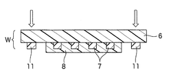
- the alignment mark 11 is formed based on the same reference as that used when forming the core 7 serving as a light path, so that the alignment mark 11 can be accurately positioned with respect to the core 7. Since the alignment mark 11 can be viewed through the transparent under-cladding layer 6 as indicated by an arrow in FIG. 8, the outer shape of the optical waveguide W is processed with high accuracy on the basis of this. Has the advantage of being able to
- the insulating layer 1 (see FIG. 7) of the electric circuit board E is usually formed of polyimide having a yellow or brown color, and therefore the colored insulating layer 1.
- the present invention has been made in view of such circumstances, and an object thereof is to provide an opto-electric hybrid board in which alignment marks for external processing are formed in an accurate and easy-to-view arrangement and a manufacturing method thereof.
- the present invention is provided with an electric circuit board in which electric wiring is formed on the surface of an insulating layer, and an optical waveguide provided on the back side of the electric circuit board, and is provided by contour processing.
- an opto-electric hybrid board having a predetermined shape is provided with an alignment mark for external processing positioned on the same basis as the electrical wiring on the surface of the insulating layer in the vicinity of the external processing portion on the surface of the insulating layer,
- a first aspect is an opto-electric hybrid board to which a predetermined shape is given by outer shape processing using the alignment mark for outer shape processing as a reference.
- the present invention has, in particular, an opto-electric hybrid board in which the alignment mark for outline processing is formed of the same material as that of the electric wiring, and among these,
- a third aspect is an opto-electric hybrid board in which the insulating layer is formed of a polyimide resin.
- the present invention also includes a step of preparing an electric circuit board having an electrical wiring formed on the surface of the insulating layer, a step of forming an optical waveguide on the back side of the electric circuit board to obtain an opto-electric hybrid board,
- a method of manufacturing an opto-electric hybrid board comprising a step of performing an outer shape process on the opto-electric hybrid board and finishing it to a predetermined shape, and in the step of preparing the electric circuit board, In the step of forming an alignment mark for outline processing that is positioned on the same basis as the electrical wiring on the surface of the insulating layer, and applying the outline processing to the opto-electric hybrid board to finish it into a predetermined shape, the alignment for the outline processing is performed.
- a method for manufacturing an opto-electric hybrid board in which outer shape processing is performed with reference to a mark is a fourth gist.
- the fifth gist is a method of manufacturing an opto-electric hybrid board in which an alignment mark for external processing is formed using the same material as that for forming an electric wiring.
- the insulating layer is particularly a polyimide resin.
- the sixth gist is a method for producing an opto-electric hybrid board using the one formed by the above method.
- the “outer shape processing” is processing for finishing the opto-electric hybrid board into a predetermined shape, and includes various types of outer shape processing by polishing or cutting in addition to cutting processing by a laser or the like. .
- the present inventors provide an alignment mark on the surface side of the colored insulating layer, not on the back surface side, to improve visibility. With the idea that it is good, I conducted extensive research. As a result, instead of forming an alignment mark at the same time as the core pattern on the back side of the insulating layer (substrate) as in the past, it is placed on the surface side of the insulating layer with high accuracy for alignment with the optical waveguide.
- the alignment mark is formed with the same standard as the electrical wiring pattern, an alignment mark with excellent positional accuracy can be obtained, and since this alignment mark is on the surface side of the insulating layer, it can be seen directly and is good It has been found that it has excellent visibility and has reached the present invention.
- the outer shape is processed with reference to the alignment mark with good visibility, which is positioned with the same reference as the electric wiring, and the electric wiring is formed on the core pattern of the optical waveguide.
- the shape given by the outer shape processing is also an accurate shape positioned with high accuracy with respect to the core pattern of the optical waveguide. Therefore, when this opto-electric hybrid board is used by being fitted to a ferrule or the like, or attached to a specific part, it can be used satisfactorily without causing problems such as poor fitting and poor connection.
- this opto-electric hybrid board has an alignment mark on the surface, in the vicinity of the outer shape processing portion, that is, toward the end of the board, further processing is performed based on the alignment mark, and product quality inspection is performed. It has the advantage that it can be performed.
- the alignment mark for external processing is formed of the same material together with the material for forming the electrical wiring
- the alignment mark is formed simultaneously with the electrical wiring. Therefore, the processing accuracy of the outer shape can be further increased, which is preferable.
- the opto-electric hybrid boards of the present invention in particular, those in which the insulating layer is formed of a polyimide-based resin do not look at the alignment mark through the yellow or brown colored insulating layer, Since the outer shape can be processed by directly viewing the alignment mark formed on the surface of the insulating layer, the practical effect is particularly great.
- the alignment mark can be accurately arranged on the surface of the insulating layer on the same basis as the electric wiring. An accurate positional relationship can be established with respect to the core pattern of the optical waveguide. Then, if the outer shape processing is performed with the alignment mark as a reference, the outer shape processing can be performed with high accuracy on the core pattern.
- the alignment mark since the alignment mark is arranged on the surface side of the opto-electric hybrid board, it can be directly recognized by a camera or the like, and can be used as a reference for processing as a clear image.
- the electric wiring is formed in the vicinity of the outline processing scheduled portion simultaneously with the formation of the electric wiring.
- the electrical wiring and the alignment mark can be formed with a single common reference, so that alignment can be performed more accurately.
- the positioning of the mark can be performed, and the outer shape can be processed with higher accuracy. And since it is not necessary to form the alignment mark independently, it is advantageous in terms of time and cost.
- an opto-electric hybrid board in which the insulating layer is formed of a polyimide resin is used for external processing regardless of whether the insulating layer is colored. Since the alignment mark can be visually recognized, the advantage is greater than the conventional manufacturing method.
- (A) is the longitudinal cross-sectional view which shows typically one Embodiment of the opto-electric hybrid board
- (b) is the partial top view.
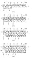
- (A) to (d) are explanatory views showing steps of producing an electric circuit board in the method for producing an opto-electric hybrid board.
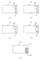
- (A) to (d) are explanatory views showing the optical waveguide manufacturing process in the method for manufacturing an opto-electric hybrid board. It is explanatory drawing which shows the external shape process in the manufacturing method of the said opto-electric hybrid board. It is explanatory drawing of the external shape process in the other example of this invention.
- (A)-(e) are explanatory drawings of the modification of the alignment mark used for this invention. It is explanatory drawing of a common opto-electric hybrid board. It is explanatory drawing of the alignment mark in the conventional optical waveguide.
- FIG. 1 (a) is a longitudinal sectional view schematically showing an example of an opto-electric hybrid board obtained by an embodiment of the present invention
- FIG. 1 (b) is a partial plan view thereof. That is, the opto-electric hybrid board 10 includes an electric circuit board E in which electric wiring 2 is provided on the surface of the insulating layer 1 and an optical waveguide W provided on the back side of the insulating layer 1.
- the electric circuit board E has an insulating layer 1 made of polyimide or the like on the surface, an optical element mounting pad 2a, an earth electrode 2b, other various element mounting pads, a connector mounting pad or the like (not shown). ) Is formed. Similarly, an alignment mark 20 made of the same material as that of the electric wiring 2 is formed on the surface of the insulating layer 1. As shown in FIG. 1B, the alignment mark 20 is provided in a strip shape in the vicinity of the edge on one side in the longitudinal direction of the opto-electric hybrid board 10 so as to cross the longitudinal direction.
- the alignment mark 20 has a processing position when performing external processing for finishing the opto-electric hybrid board 10 into a predetermined shape. It is used as a reference for determining, and providing the alignment mark 20 in this arrangement is a major feature of the present invention.
- the electrical wiring 2 excluding the alignment mark 20 and the pad 2a is insulated and protected by a cover lay 3 made of polyimide or the like. Note that the surfaces of the alignment marks 20 and the pads 2a exposed from the coverlay 3 are covered and protected with an electrolytic plating layer 4 made of gold, nickel, or the like.
- the optical waveguide W provided on the back surface side of the insulating layer 1 covers the under cladding layer 6, the core 7 formed in a predetermined pattern on the surface (the lower surface in FIG. 1), and the core 7.
- the over-cladding layer 8 is integrated with the surface of the under-cladding layer 6 in a state.
- Reference numeral 9 denotes a metal layer provided on the back surface of the insulating layer 1 in order to reinforce the opto-electric hybrid board 10 and is formed in a pattern excluding a portion where flexibility is required.
- the metal layer 9 has a through hole 5 for securing an optical path between the core 7 and the optical element.
- the under cladding layer 6 also enters the through hole 5. .
- the metal layer 9 is formed as necessary and is not necessarily required.
- the portion of the core 7 corresponding to the optical element mounting pad 2a of the electric circuit board E is formed on an inclined surface of 45 ° with respect to the extending direction of the core 7.
- This inclined surface is a light reflecting surface 7a, which changes the direction of the light propagated in the core 7 by 90 ° to enter the light receiving portion of the optical element, or conversely, exits from the light emitting portion of the optical element.
- the direction of the emitted light is changed by 90 ° to enter the core 7.
- the opto-electric hybrid board 10 can be obtained, for example, as follows by the manufacturing method of the present invention (see FIGS. 2 to 4).
- a flat metal layer 9 is prepared, a photosensitive insulating resin made of polyimide or the like is applied to the surface, and a predetermined pattern of the insulating layer 1 is formed by photolithography.
- a predetermined pattern of the insulating layer 1 is formed by photolithography.
- the thickness of the insulating layer 1 is set within a range of 3 to 50 ⁇ m, for example.
- the material for forming the metal layer 9 include stainless steel, copper, silver, aluminum, nickel, chromium, titanium, platinum, and gold. Among them, stainless steel is preferable from the viewpoint of rigidity and the like. Further, although the thickness of the metal layer 9 depends on the material, it is set within a range of 10 to 70 ⁇ m, for example, when stainless steel is used.
- an electrical wiring 2 including an optical element mounting pad 2a, an earth electrode 2b, other pads, and so on;
- the alignment mark 20 for outline processing is simultaneously formed by, for example, a semi-additive method.
- a metal film (not shown) made of copper, chromium, or the like is formed on the surface of the insulating layer 1 by sputtering or electroless plating. This metal film becomes a seed layer (layer serving as a base for forming an electrolytic plating layer) when performing subsequent electrolytic plating.
- a photosensitive resist (not shown) on both surfaces of the laminate composed of the metal layer 9, the insulating layer 1 and the seed layer
- a photo resist is applied to the photosensitive resist on the side where the seed layer is formed.
- a hole portion of the pattern of the electric wiring 2 is formed by lithography, and the surface portion of the seed layer is exposed at the bottom of the hole portion.
- an electrolytic plating layer made of copper or the like is laminated on the surface portion of the seed layer exposed to the bottom of the hole by electrolytic plating.
- the photosensitive resist is removed with an aqueous sodium hydroxide solution or the like. Thereafter, the portion of the seed layer where the electrolytic plating layer is not formed is removed by soft etching.
- the laminated portion composed of the remaining seed layer and electrolytic plating layer becomes the electric wiring 2 and the alignment mark 20.
- a photosensitive insulating resin made of polyimide or the like is applied to a portion of the electrical wiring 2 excluding the pad 2a for mounting the optical element and other pads, and by photolithography, A coverlay 3 is formed.
- the electroplating layer 4 is formed on the surface of the alignment mark 20 and the pad 2a for mounting the optical element and other pads. In this way, the electric circuit board E is formed.
- a photosensitive resist is laminated on both sides of the laminate composed of the metal layer 9 and the electric circuit board E, and then the back side of the metal layer 9 (the side opposite to the electric circuit board E) is exposed.
- the conductive resist holes are formed by photolithography in portions corresponding to the portions where the metal layer 9 is not required and the through-hole formation planned portion for the optical path, and the back surface of the metal layer 9 is partially exposed. .
- the exposed portion of the metal layer 9 is etched using an aqueous solution for etching corresponding to the metal material of the metal layer 9 (for example, the aqueous solution for etching when the metal layer 9 is a stainless steel layer is ferric chloride aqueous solution).
- the insulating layer 1 is exposed from the trace of the removal, and then the photosensitive resist is peeled off with an aqueous sodium hydroxide solution or the like.
- the metal layer 9 is formed only in the region requiring reinforcement, and the through hole 5 for the optical path is also formed at the same time.
- the optical waveguide W (see FIG. 1A) on the back surface of the insulating layer 1 (the back surface of the metal layer 9 in the portion where the metal layer 9 is formed)
- a photosensitive resin which is a material for forming the undercladding layer 6
- the applied layer is irradiated with radiation.
- the under cladding layer 6 can be formed in a predetermined pattern by a photolithography method.
- the under clad layer 6 is formed in a state where the metal layer 9 enters and fills the through hole 5 for the optical path.
- the thickness of the under cladding layer 6 (thickness from the back surface of the insulating layer 1) is usually set to be thicker than the thickness of the metal layer 9.
- a series of operations for forming the optical waveguide W is performed with the back surface of the insulating layer 1 on which the metal layer 9 is formed facing upward, but is shown as it is in the drawing.
- a core 7 having a predetermined pattern is formed on the surface (the lower surface in the drawing) of the under cladding layer 6 by photolithography.
- the thickness of the core 7 is set within a range of 3 to 100 ⁇ m, for example, and the width is set within a range of 3 to 100 ⁇ m, for example.
- the material for forming the core 7 include the same photosensitive resin as that for the under cladding layer 6, and a material having a higher refractive index than the material for forming the under cladding layer 6 and an over cladding layer 8 described later is used. It is done.
- the adjustment of the refractive index can be performed, for example, by selecting the types of forming materials of the under cladding layer 6, the core 7, and the over cladding layer 8 and adjusting the composition ratio.
- an over clad layer 8 is formed by photolithography so as to cover the core 7 so as to cover the surface of the under clad layer 6 (lower surface in the figure).
- the optical waveguide W is formed.
- the thickness of the over cladding layer 8 is set to be not less than the thickness of the core 7 and not more than 300 ⁇ m, for example.
- Examples of the material for forming the over cladding layer 8 include the same photosensitive resin as that for the under cladding layer 6.
- an optical element mounted on the surface side of the electric circuit board E is formed on the predetermined portion of the optical waveguide W by forming an inclined surface inclined by 45 ° with respect to the extending direction of the core 7 by laser processing or cutting processing. It is assumed that the reflecting surface 7a [see FIG. Then, necessary members are attached, such as mounting an optical element on the pad 2a of the electric wiring 2 provided on the surface side of the electric circuit board E.
- the electrical mixed substrate 10 (however, the outer shape is not processed). Then, as shown in FIG. 4, while visually confirming the alignment mark 20 with an alignment camera or the like, a position away from the alignment mark 20 by a predetermined distance is specified as a cutting position, and this irradiation is performed by laser irradiation (for example, YAG laser). Cut the part.
- laser irradiation for example, YAG laser
- various cutting means such as a dicing saw can be used in addition to laser irradiation.
- the thus obtained opto-electric hybrid board 10 (with the outer shape processed) was formed on the same basis as the electric wiring 2 provided in the vicinity of one end in the longitudinal direction of the opto-electric hybrid board 10. Since the end face of the alignment mark 20 is cut with high dimensional accuracy, the overall outer dimensions are accurate and there is no dimensional variation. Therefore, when this is used by fitting with a ferrule or the like or when it is attached to a specific part, it can be used satisfactorily without causing problems such as poor fitting or poor connection. Further, with this alignment mark 20 as a reference, further processing or product quality inspection can be performed.
- the alignment mark 20 for outer shape processing is not provided on the processing line (cutting line in this example) for outer shape processing, but is provided in the vicinity of the processing line apart from the processing line. Therefore, in laser processing or dicing processing, the alignment mark 20 has an advantage that the processing is not affected and a good finish can be obtained. That is, when the alignment mark 20 made of a metal material is provided on the processing line, in laser processing or the like, the processing speed differs between a portion where the alignment mark 20 is present and a portion where the alignment mark 20 is not present, and thus there is a risk of rattling at the boundary portion. is there.
- the metal powder generated by the polishing may damage the end surface. If such a backlash or scratch is present on the finished surface where high processing accuracy is required, light loss may be caused. Therefore, when the alignment mark 20 is not on the processing line and is provided only in the vicinity thereof as in the above example, an excellent finished product is obtained in combination with the high positional accuracy. .
- one end edge of the opto-electric hybrid board 10 produced longer than the finally required length is cut to finish the opto-electric hybrid board 10 of an appropriate length.
- FIG. 5 for example, when a predetermined length of the opto-electric hybrid substrate 10 is continuously cut out from the intermediate product 10 ′ of the opto-electric hybrid substrate manufactured in a long shape by a roll-to-roll method, one point is obtained.
- the alignment mark 20 can be used as a reference for specifying a cutting position indicated by a chain line P. While confirming the alignment mark 20 with an alignment camera or the like in sequence, positioning and cutting at an appropriate position can continuously obtain an opto-electric hybrid board 10 having a proper length without variation. .
- various outer shape processing for processing the outer shape of the opto-electric hybrid board 10 into a desired shape according to the shape of the mating member to which the opto-electric hybrid board 10 is fitted or attached. It is effective to use the alignment mark 20 as a dimensional reference for the processing (including processing and polishing).
- the shape of the alignment mark 20 in plan view is not limited to a single band as shown in FIG. 1B, and for example, as shown in FIGS.
- the alignment marks 20 may be arranged along the vicinity of the cutting position indicated by the alternate long and short dash line P. Further, as shown in FIG. 6E, a set of two alignment marks 20 each having a cross shape may be provided across the cutting position. Similarly, the fixed region may be completely covered with the electric wiring material, and the inner side thereof may be formed into a circular or polygonal shape to form the alignment mark 20. Thus, in any case, for the reasons described above, it is desirable that the alignment mark 20 is not located on the cutting position P but only in the vicinity thereof.
- the cover lay 3 is not provided on the alignment mark 20, and the surface is covered and protected with the electrolytic plating layer 4.
- the alignment mark 20 may be sufficiently visible through the coverlay 3. In that case, the alignment mark 20 may be covered with the cover lay 3 as in the case of the other electric wirings 2.
- the light reflecting surface 7 a (see FIG. 1A) is formed on the core 7 using the material for forming the electrical wiring 2.
- a positioning alignment mark and an optical element positioning alignment mark can be formed simultaneously, or a single alignment mark serving as both can be formed simultaneously (see Japanese Patent Application No. 2013-224450). Therefore, if the alignment mark 20 for external processing is simultaneously formed together with these alignment marks, the formation of the electrical wiring 2 and the formation of the various alignment marks 20 and the like can be performed in a single step in a single process. Since it can be performed on the basis, it is possible to obtain the high-quality opto-electric hybrid board 10 with higher accuracy of the mutual positional relationship, which is preferable.
- the alignment mark 20 for external processing is formed at the same time as the electric wiring 2, but in the present invention, the alignment mark 20 and the electric wiring 2 are not necessarily formed at the same time. . In some cases, either one may be formed first and then the other based on the same standard. However, as shown in the previous example, it is preferable to form both at the same time because the positional relationship between the two becomes more accurate.
- the present invention can be used for providing an opto-electric hybrid board having a stable quality that is excellent in dimensional accuracy of an outer shape and does not cause inconvenience in fitting with other members or attachment to a predetermined position. it can.
Landscapes
- Physics & Mathematics (AREA)
- Engineering & Computer Science (AREA)
- Microelectronics & Electronic Packaging (AREA)
- General Physics & Mathematics (AREA)
- Optics & Photonics (AREA)
- Manufacturing & Machinery (AREA)
- Optical Integrated Circuits (AREA)
- Structure Of Printed Boards (AREA)
Abstract
Description
<アンダークラッド層6、オーバークラッド層8の形成材料>
脂環骨格を含むエポキシ樹脂(ダイセル化学工業社製、EHPE3150) 20重量部
液状長鎖二官能半脂肪族エポキシ樹脂(DIC社製、EXA-4816) 80重量部
光酸発生剤(ADEKA社製、SP170) 2重量部
乳酸エチル(武蔵野化学研究所社製) 40重量部
<コア7の形成材料>
o-クレゾールノボラックグリシジルエーテル(新日鐵住金化学社製、YDCN-700-10) 50重量部
ビスフェノキシエタノールフルオレンジグリシジルエーテル(大阪ガスケミカル社製、オグゾールEG) 50重量部
光酸発生剤(ADEKA社製、SP170) 1重量部
乳酸エチル(武蔵野化学研究所社製) 50重量部
W 光導波路
1 絶縁層
2 電気配線
10 光電気混載基板
20 アライメントマーク
Claims (6)
- 絶縁層の表面に電気配線が形成された電気回路基板と、上記電気回路基板の裏面側に設けられる光導波路とを備えるとともに、外形加工によって付与された所定形状を有する光電気混載基板であって、上記絶縁層表面の外形加工部の近傍に、絶縁層表面の電気配線と同一基準で位置決めされた外形加工用のアライメントマークが設けられており、上記外形加工用のアライメントマークを基準とした外形加工によって所定形状が付与されていることを特徴とする光電気混載基板。
- 上記外形加工用のアライメントマークが、上記電気配線の形成材料と同一材料によって形成されている請求項1記載の光電気混載基板。
- 上記絶縁層が、ポリイミド系樹脂によって形成されている請求項1または2記載の光電気混載基板。
- 絶縁層の表面に電気配線が形成された電気回路基板を準備する工程と、この電気回路基板の裏面側に光導波路を形成して光電気混載基板を得る工程と、上記光電気混載基板に外形加工を施して所定形状に仕上げる工程とを備えた光電気混載基板の製法であって、上記電気回路基板を準備する工程において、絶縁層表面の外形加工予定部の近傍に、絶縁層表面の電気配線と同一基準で位置決めされた外形加工用のアライメントマークを形成しておき、上記光電気混載基板に外形加工を施して所定形状に仕上げる工程において、上記外形加工用のアライメントマークを基準として外形加工を行うようにしたことを特徴とする光電気混載基板の製法。
- 上記電気回路基板を準備する工程において、絶縁層表面に電気配線を形成する際、その電気配線の形成と同時に、外形加工予定部の近傍に、上記電気配線の形成材料と同一材料を用いて外形加工用のアライメントマークを形成するようにした請求項4記載の光電気混載基板の製法。
- 上記絶縁層がポリイミド系樹脂によって形成されたものを用いる請求項4または5記載の光電気混載基板の製法。
Priority Applications (3)
| Application Number | Priority Date | Filing Date | Title |
|---|---|---|---|
| KR1020177008729A KR20170076656A (ko) | 2014-10-24 | 2015-10-09 | 광전기 혼재 기판 및 그 제법 |
| US15/517,267 US10073232B2 (en) | 2014-10-24 | 2015-10-09 | Opto-electric hybrid board, and production method therefor |
| CN201580053308.5A CN106796325B (zh) | 2014-10-24 | 2015-10-09 | 光电混载基板及其制造方法 |
Applications Claiming Priority (2)
| Application Number | Priority Date | Filing Date | Title |
|---|---|---|---|
| JP2014-217133 | 2014-10-24 | ||
| JP2014217133A JP6525240B2 (ja) | 2014-10-24 | 2014-10-24 | 光電気混載基板およびその製法 |
Publications (1)
| Publication Number | Publication Date |
|---|---|
| WO2016063752A1 true WO2016063752A1 (ja) | 2016-04-28 |
Family
ID=55760796
Family Applications (1)
| Application Number | Title | Priority Date | Filing Date |
|---|---|---|---|
| PCT/JP2015/078820 Ceased WO2016063752A1 (ja) | 2014-10-24 | 2015-10-09 | 光電気混載基板およびその製法 |
Country Status (6)
| Country | Link |
|---|---|
| US (1) | US10073232B2 (ja) |
| JP (1) | JP6525240B2 (ja) |
| KR (1) | KR20170076656A (ja) |
| CN (1) | CN106796325B (ja) |
| TW (1) | TWI670535B (ja) |
| WO (1) | WO2016063752A1 (ja) |
Families Citing this family (7)
| Publication number | Priority date | Publication date | Assignee | Title |
|---|---|---|---|---|
| JP7076968B2 (ja) * | 2017-08-22 | 2022-05-30 | 日東電工株式会社 | 光導波路、光電気混載基板および光電気混載モジュール |
| JP6677232B2 (ja) * | 2017-09-29 | 2020-04-08 | 日亜化学工業株式会社 | 発光装置の製造方法 |
| JP2019175943A (ja) * | 2018-03-27 | 2019-10-10 | シャープ株式会社 | フレキシブルプリント基板、積層体、およびフレキシブルプリント基板の製造方法 |
| JP2020016756A (ja) * | 2018-07-25 | 2020-01-30 | 日東電工株式会社 | 光導波路部材コネクタおよびその製造方法 |
| TWI664885B (zh) * | 2018-09-14 | 2019-07-01 | 友達光電股份有限公司 | 雙面線路基板的製造方法與雙面線路基板 |
| CN111526664A (zh) * | 2020-04-28 | 2020-08-11 | 苏州狮威电子科技有限公司 | 一种电路板bin值标记方法 |
| TW202234103A (zh) * | 2020-09-30 | 2022-09-01 | 日商日東電工股份有限公司 | 光電混合基板、安裝光元件之光電混合基板及該安裝光元件之光電混合基板之製造方法 |
Citations (7)
| Publication number | Priority date | Publication date | Assignee | Title |
|---|---|---|---|---|
| JP2004294857A (ja) * | 2003-03-27 | 2004-10-21 | Fujitsu Ltd | 光結合器及び光素子内蔵基板 |
| JP2007241190A (ja) * | 2006-03-13 | 2007-09-20 | Toppan Printing Co Ltd | 光基板の製造方法及び光基板 |
| JP2008158221A (ja) * | 2006-12-22 | 2008-07-10 | Matsushita Electric Works Ltd | 光電複合基板の製造方法 |
| JP2009031582A (ja) * | 2007-07-27 | 2009-02-12 | Fuji Xerox Co Ltd | 光導波路の製造方法 |
| JP2010128200A (ja) * | 2008-11-27 | 2010-06-10 | Nitto Denko Corp | 光電気混載基板およびその製造方法 |
| JP2012163649A (ja) * | 2011-02-04 | 2012-08-30 | Hitachi Cable Ltd | 光モジュール |
| JP2015087475A (ja) * | 2013-10-29 | 2015-05-07 | 日東電工株式会社 | 光電気混載基板およびその製法 |
Family Cites Families (15)
| Publication number | Priority date | Publication date | Assignee | Title |
|---|---|---|---|---|
| JP4967803B2 (ja) * | 2006-05-18 | 2012-07-04 | 凸版印刷株式会社 | 光電気複合基板の製造方法 |
| KR101084407B1 (ko) * | 2006-12-26 | 2011-11-18 | 미쓰이 가가쿠 가부시키가이샤 | 광 전기 혼재 기판 및 그의 제조 방법 |
| JP2009036924A (ja) * | 2007-07-31 | 2009-02-19 | Nitto Denko Corp | 光導波路フィルム、光基板およびこれらの製造方法 |
| JP5055193B2 (ja) * | 2008-04-24 | 2012-10-24 | 日東電工株式会社 | 光電気混載基板の製造方法 |
| US20100034497A1 (en) * | 2008-08-05 | 2010-02-11 | Fujitsu Limited | Flexible Optical Pillars for an Optical Assembly |
| JP5106348B2 (ja) * | 2008-10-28 | 2012-12-26 | 日東電工株式会社 | 光電気混載モジュールの製造方法およびそれによって得られた光電気混載モジュール |
| JP4796615B2 (ja) * | 2008-11-26 | 2011-10-19 | 日東電工株式会社 | 光電気混載基板およびその製造方法 |
| CH700471B1 (de) * | 2009-02-17 | 2013-07-31 | Vario Optics Ag | Verfahren zur Herstellung einer elektro-optischen Leiterplatte mit Lichtwellenleiterstrukturen. |
| JP2011085647A (ja) * | 2009-10-13 | 2011-04-28 | Hitachi Chem Co Ltd | 光導波路基板及びその製造方法 |
| JP2012155215A (ja) * | 2011-01-27 | 2012-08-16 | Nitto Denko Corp | 光導波路の製法およびそれに用いられる光導波路体 |
| JP5820266B2 (ja) * | 2011-12-26 | 2015-11-24 | 日東電工株式会社 | 光導波路形成用樹脂組成物およびそれを用いた光導波路 |
| JP5840989B2 (ja) * | 2012-03-16 | 2016-01-06 | 日東電工株式会社 | 光電気混載基板およびその製法 |
| JP5877749B2 (ja) * | 2012-03-29 | 2016-03-08 | 日東電工株式会社 | 光電気混載基板の製法 |
| JP6202662B2 (ja) * | 2012-11-27 | 2017-09-27 | 日東電工株式会社 | 光電気混載基板およびその製法 |
| JP6175263B2 (ja) * | 2013-03-28 | 2017-08-02 | 富士通株式会社 | スポットサイズ変換器、その製造方法及び光集積回路装置 |
-
2014
- 2014-10-24 JP JP2014217133A patent/JP6525240B2/ja not_active Expired - Fee Related
-
2015
- 2015-10-08 TW TW104133248A patent/TWI670535B/zh not_active IP Right Cessation
- 2015-10-09 US US15/517,267 patent/US10073232B2/en active Active
- 2015-10-09 KR KR1020177008729A patent/KR20170076656A/ko not_active Abandoned
- 2015-10-09 CN CN201580053308.5A patent/CN106796325B/zh not_active Expired - Fee Related
- 2015-10-09 WO PCT/JP2015/078820 patent/WO2016063752A1/ja not_active Ceased
Patent Citations (7)
| Publication number | Priority date | Publication date | Assignee | Title |
|---|---|---|---|---|
| JP2004294857A (ja) * | 2003-03-27 | 2004-10-21 | Fujitsu Ltd | 光結合器及び光素子内蔵基板 |
| JP2007241190A (ja) * | 2006-03-13 | 2007-09-20 | Toppan Printing Co Ltd | 光基板の製造方法及び光基板 |
| JP2008158221A (ja) * | 2006-12-22 | 2008-07-10 | Matsushita Electric Works Ltd | 光電複合基板の製造方法 |
| JP2009031582A (ja) * | 2007-07-27 | 2009-02-12 | Fuji Xerox Co Ltd | 光導波路の製造方法 |
| JP2010128200A (ja) * | 2008-11-27 | 2010-06-10 | Nitto Denko Corp | 光電気混載基板およびその製造方法 |
| JP2012163649A (ja) * | 2011-02-04 | 2012-08-30 | Hitachi Cable Ltd | 光モジュール |
| JP2015087475A (ja) * | 2013-10-29 | 2015-05-07 | 日東電工株式会社 | 光電気混載基板およびその製法 |
Also Published As
| Publication number | Publication date |
|---|---|
| CN106796325A (zh) | 2017-05-31 |
| JP6525240B2 (ja) | 2019-06-05 |
| TWI670535B (zh) | 2019-09-01 |
| JP2016085315A (ja) | 2016-05-19 |
| KR20170076656A (ko) | 2017-07-04 |
| TW201626014A (zh) | 2016-07-16 |
| US10073232B2 (en) | 2018-09-11 |
| US20170307833A1 (en) | 2017-10-26 |
| CN106796325B (zh) | 2021-07-23 |
Similar Documents
| Publication | Publication Date | Title |
|---|---|---|
| WO2016063752A1 (ja) | 光電気混載基板およびその製法 | |
| JP6202566B2 (ja) | 光電気混載基板およびその製法 | |
| JP5877749B2 (ja) | 光電気混載基板の製法 | |
| US10606002B2 (en) | Opto-electric hybrid board and manufacturing method for same | |
| JP5608125B2 (ja) | 光電気混載基板およびその製法 | |
| US10288823B2 (en) | Opto-electric hybrid board | |
| US10353161B2 (en) | Opto-electric hybrid board and method of manufacturing same | |
| JP6653857B2 (ja) | 光電気混載基板およびその製法 | |
| JP5674516B2 (ja) | 光電気混載基板およびその製法 | |
| JP6460516B2 (ja) | 光電気混載基板 | |
| WO2016047447A1 (ja) | 光電気混載基板およびその製法 | |
| WO2017163634A1 (ja) | 光導波路積層体およびその製法 | |
| JP5674525B2 (ja) | 光電気混載基板の製法 | |
| WO2016084815A1 (ja) | 光電気混載基板およびその製法 |
Legal Events
| Date | Code | Title | Description |
|---|---|---|---|
| 121 | Ep: the epo has been informed by wipo that ep was designated in this application |
Ref document number: 15851831 Country of ref document: EP Kind code of ref document: A1 |
|
| ENP | Entry into the national phase |
Ref document number: 20177008729 Country of ref document: KR Kind code of ref document: A |
|
| WWE | Wipo information: entry into national phase |
Ref document number: 15517267 Country of ref document: US |
|
| NENP | Non-entry into the national phase |
Ref country code: DE |
|
| 122 | Ep: pct application non-entry in european phase |
Ref document number: 15851831 Country of ref document: EP Kind code of ref document: A1 |