WO2016046952A1 - ウエハ搬送装置 - Google Patents
ウエハ搬送装置 Download PDFInfo
- Publication number
- WO2016046952A1 WO2016046952A1 PCT/JP2014/075600 JP2014075600W WO2016046952A1 WO 2016046952 A1 WO2016046952 A1 WO 2016046952A1 JP 2014075600 W JP2014075600 W JP 2014075600W WO 2016046952 A1 WO2016046952 A1 WO 2016046952A1
- Authority
- WO
- WIPO (PCT)
- Prior art keywords
- wafer
- identification
- identification code
- clamp
- peripheral edge
- Prior art date
- Legal status (The legal status is an assumption and is not a legal conclusion. Google has not performed a legal analysis and makes no representation as to the accuracy of the status listed.)
- Ceased
Links
Images



Classifications
-
- H—ELECTRICITY
- H05—ELECTRIC TECHNIQUES NOT OTHERWISE PROVIDED FOR
- H05K—PRINTED CIRCUITS; CASINGS OR CONSTRUCTIONAL DETAILS OF ELECTRIC APPARATUS; MANUFACTURE OF ASSEMBLAGES OF ELECTRICAL COMPONENTS
- H05K13/00—Apparatus or processes specially adapted for manufacturing or adjusting assemblages of electric components
- H05K13/02—Feeding of components
-
- H—ELECTRICITY
- H10—SEMICONDUCTOR DEVICES; ELECTRIC SOLID-STATE DEVICES NOT OTHERWISE PROVIDED FOR
- H10P—GENERIC PROCESSES OR APPARATUS FOR THE MANUFACTURE OR TREATMENT OF DEVICES COVERED BY CLASS H10
- H10P72/00—Handling or holding of wafers, substrates or devices during manufacture or treatment thereof
- H10P72/30—Handling or holding of wafers, substrates or devices during manufacture or treatment thereof for conveying, e.g. between different workstations
Definitions
- the present invention relates to a wafer transfer apparatus that takes out and transfers a predetermined wafer from a magazine that stores a plurality of wafers in a stacked state.
- the wafer transfer apparatus is applied to an apparatus for supplying a wafer as a kind of a component supply apparatus of a component mounter, for example, as disclosed in Patent Document 1.
- the wafer transfer device pulls out the wafer from the magazine and allows the component mounter to pick up the wafer cut component (chip). Transport to the supply position.
- the component supply device grasps which wafer is stored in each slot of the magazine based on, for example, a setting file for the magazine.
- the component supply apparatus controls the wafer transfer apparatus so that the wafer designated by the supply request is pulled out from the corresponding slot. Further, as a method for pulling out a specific wafer from a magazine in a wafer transfer device, for example, as shown in Patent Document 2, a method is known in which a peripheral portion of a wafer is held and moved by a clamp portion.
- the wafer transfer device identifies the unique identification code attached to each wafer by the identification device, and determines whether the wafer being transferred is a specified wafer based on the identification information included in the identification code. Determine whether or not.
- the identification code is covered by the clamp unit and the identification device identifies the identification code.
- the clamp portion is temporarily retracted from the wafer in a state where the peripheral portion of the wafer to which the identification code is attached is exposed to the outside of the magazine.
- the identification code is exposed, and the identification device can identify the identification code.
- the cycle time may be extended with an increase in operations in the transport process.
- the present invention has been made in view of such circumstances, and an object of the present invention is to provide a wafer transfer apparatus that enables an identification code to be identified by an identification apparatus in a state where a clamp portion grips a wafer.
- the wafer transfer apparatus takes out the predetermined wafer from a magazine that accommodates a plurality of stacked wafers and transfers the wafer.
- An identification code including identification information used for specifying the wafer is attached to the peripheral portion of the wafer.
- the wafer transfer device includes: a clamp unit that grips the peripheral portion of the wafer; a drive unit that moves the clamp unit in the transfer direction of the wafer; and the wafer that is at least partially removed from the magazine. And an identification device that identifies the identification code by receiving reflected light reflected by the identification code of the wafer.
- the clamp portion is formed of a material that transmits the reflected light reflected by the identification code, and the identification code of the identification device by the identification device is held in a state where the peripheral portion of the wafer to which the identification code is attached is gripped. Allows identification.
- the identification device can identify the identification code without opening the clamp portion and retracting it.
- FIG. 1 It is a perspective view showing the whole component mounting machine in an embodiment. It is a side view which shows the component supply apparatus of the component mounting machine of FIG. It is a top view which shows the clamp part and wafer of FIG. It is an enlarged view which shows the clamp part and identification code in FIG. It is a block diagram which shows a wafer conveyance apparatus. It is a flowchart which shows the conveyance process of the wafer by a wafer conveyance apparatus.
- a wafer transfer apparatus of the present invention is embodied.
- the component supply device supplies a predetermined electronic component so that it can be picked up by the component mounter in response to a request from the component mounter that mounts the electronic component on the circuit board.
- the component mounter 1 includes a substrate transfer device 2, a component supply device 3, and a component transfer device 4.
- the horizontal width direction of the component mounter 1 (the direction from the upper left to the lower right in FIG. 1) is the X-axis direction
- the horizontal longitudinal direction of the component mounter 1 (the direction from the upper right to the lower left in FIG. 1).
- the vertical direction (vertical direction in FIG. 1) perpendicular to the X-axis and Y-axis is the Z-axis direction.
- the substrate transfer device 2 is configured by a belt conveyor or the like, and sequentially transfers the circuit board Bd in the transfer direction (X-axis direction).
- the board conveying device 2 positions the circuit board Bd at a predetermined position in the component mounting machine 1. Then, after the mounting process by the component mounter 1 is executed, the board transfer device 2 carries the circuit board Bd out of the component mounter 1.
- the component supply device 3 supplies electronic components to be mounted on the circuit board Bd.
- the above-described electronic components include electronic components accommodated in a carrier tape at a predetermined pitch, and chips 91 obtained by cutting the wafer 90 in units of components.
- the carrier tape is fed and moved by a feeder that is detachably set in a plurality of slots of the component supply device 3.
- the component supply apparatus 3 supplies an electronic component in the taking-out part of the front end side of a feeder.
- the component mounter 1 also includes a wafer supply device 20 that supplies a chip 91 of the wafer 90 as a kind of the component supply device 3. The detailed configuration of the wafer supply apparatus 20 will be described later.
- the wafer 90 has a plurality of chips 91, an adhesive sheet 92, a ring frame 93, and a bar code 94 (corresponding to the “identification code” of the present invention).
- a plurality of chips 91 are formed, for example, in a lattice pattern on the wafer body, and are cut into parts by a laser cutter or the like while being attached to the adhesive sheet 92.
- the ring frame 93 is an annular plate member.
- the ring frame 93 holds the pressure-sensitive adhesive sheet 92 that is expanded in the radial direction.
- the plurality of chips 91 are separated from each other at the opening of the ring frame 93.
- the wafer 90 has a plate shape as a whole, and the whole shape is held by the ring frame 93 that functions as an outer frame.
- an identification code used for specifying the wafer 90 is attached to the peripheral portion of the wafer 90 (the ring frame 93 in the present embodiment).
- the identification code any of a barcode, a two-dimensional code, a character string, a pattern, a color, or a combination thereof can be adopted.
- the identification code employs a bar code 94 configured by arranging a plurality of bar lines having different line widths and intervals between lines in parallel.
- the component transfer device 4 is configured to be movable in the X-axis direction and the Y-axis direction.
- the component transfer device 4 is arranged from the rear side in the longitudinal direction of the component mounter 1 (upper right side in FIG. 1) to the upper side of the component supply device 3 on the front side.
- the component transfer device 4 includes a head driving device 11 and a mounting head 12.
- the head driving device 11 is configured to be able to move the moving table in the XY axis directions by a linear motion mechanism.
- the mounting head 12 is detachably provided on the moving table of the head driving device 11.
- the mounting head 12 is provided with a plurality of suction nozzles 13 detachably.
- the mounting head 12 supports each of the suction nozzles 13 so as to be rotatable about the R axis parallel to the Z axis and to be movable up and down.
- Each suction nozzle 13 is controlled in the elevation position and angle with respect to the mounting head 12 and the supply state of negative pressure.
- Each suction nozzle 13 sucks and holds the electronic components supplied at the feeder take-out portion and the chips 91 of the wafer 90 supplied by the wafer supply device 20 by being supplied with a negative pressure.
- the wafer supply device 20 includes a storage device 21, a magazine 30, a wafer transfer device 40, and a push-up device 80.
- the storage device 21 stores a setting file for a magazine that records which wafer 90 is accommodated in each slot of the magazine 30.
- the magazine 30 includes a housing 31, a wafer stocker 32, and a stocker lifting device 33.
- the housing 31 is formed in a rectangular parallelepiped shape.
- a slit 31 a into which the wafer 90 can be carried in and out is formed in a portion of the outer peripheral surface facing the component supply position Ps where the component transfer device 4 picks up an electronic component.
- the wafer stocker 32 is provided inside the housing 31 so as to be movable up and down.
- the wafer stocker 32 stores a plurality of wafers 90 in a stacked state. More specifically, the wafer stocker 32 is formed with a plurality of slots arranged at equal intervals in the Z-axis direction, and a wafer 90 is accommodated in each slot so as to be slidable in the Y-axis direction.
- the stocker raising / lowering device 33 is arranged inside the housing 31 so that the wafer stocker 32 can be raised and lowered.
- the stocker lifting / lowering device 33 supports a wafer stocker 32 provided so as to be movable up and down relative to the housing 31.
- the stocker raising / lowering device 33 is constituted by, for example, a motor and a ball screw mechanism, and raises and lowers the wafer stocker 32 to a predetermined vertical position with respect to the housing 31.
- the magazine 30 raises and lowers the wafer stocker 32 based on the control command so that the predetermined wafer 90 can be carried out from the slit 31a of the housing 31.
- the magazine 30 enables the wafer 90 to be loaded into the empty slot by positioning the empty slot of the wafer stocker 32 at the vertical position corresponding to the slit 31 a of the housing 31.
- the wafer transfer device 40 takes out a predetermined wafer 90 from the magazine 30 and transfers it.
- the wafer transfer device 40 includes a clamp unit 41, an arm 42, a wafer table 43, a drive device 50, an identification device 60, and a control device 70.
- the clamp portion 41 is configured to be able to grip a front peripheral edge portion 93 a of the wafer 90 at a vertical position corresponding to the slit 31 a of the housing 31 among the plurality of wafers 90 accommodated in the wafer stocker 32.
- the detailed configuration of the clamp part 41 will be described later.
- the base end portion of the arm 42 is fixed to the driving device 50.
- the distal end portion of the arm 42 supports the clamp portion 41.
- the wafer table 43 is arranged at a component supply position Ps where the component transfer device 4 can pick up an electronic component (chip 91).
- the wafer table 43 is configured to be able to hold a ring frame 93 of the wafer 90 transferred upward.
- the driving device 50 is a loader that moves the clamp unit 41 in the transport direction (left-right direction in FIG. 2) via the arm 42. Further, the driving device 50 operates an actuator (not shown) provided in the clamp unit 41 to switch between the gripping state and the open state of the clamp unit 41.
- the drive device 50 includes a slide body 51, a guide rail 52, an endless belt 53, and a servo motor 54.
- the slide body 51 of the driving device 50 supports the base end portion of the arm 42.
- the slide body 51 is guided by a guide rail 52 extending in the Y-axis direction so as to be movable along the transport direction.
- the slide body 51 is fixed to a part of the endless belt 53.
- the endless belt 53 is suspended by a pair of pulleys (not shown), and rotates by driving a servo motor 54 connected to the rotation shaft of one pulley.
- the driving device 50 drives the servo motor 54 based on the control command to reciprocate the clamp unit 41 in the transport direction via the endless belt 53, the slide body 51, and the arm 42.
- the driving device 50 synchronizes the gripping operation for switching the gripping state and the open state of the clamp unit 41 to carry out the wafer 90 pulled out from the magazine 30 to the wafer table 43, and the wafer table 43. Then, the wafer 90 is loaded into the magazine 30.
- the identification device 60 identifies the barcode 94 by receiving the reflected light reflected by the barcode 94 of the wafer 90 for the wafer 90 in a state where at least a part is taken out from the magazine 30.
- the identification information included in the barcode 94 is read.
- the identification device 60 is provided on an upper portion of the outer peripheral surface of the housing 31 where the slit 31 a is formed.
- the identification device 60 includes a sensor unit 61 that receives the reflected light reflected by the barcode 94. With such a configuration, the identification device 60 can identify the barcode 94 in the identification region Rs adjacent to the slit 31a of the housing 31, as shown in FIG. That is, the identification device 60 reads the identification information of the barcode 94 attached to the wafer 90 for the wafer 90 that is partially pulled out from the magazine 30.
- the control device 70 is mainly composed of a CPU, various memories, and a control circuit.
- the control device 70 is connected to the driving device 50 and the identification device 60 through an interface circuit, and controls the transfer processing of the wafer 90 by the wafer transfer device 40.
- the control device 70 includes a conveyance control unit 71 and a code presence / absence determination unit 72.
- the transfer control unit 71 executes transfer processing of the wafer 90 by the wafer transfer device 40 based on the control command of the wafer supply device 20.
- the transfer control unit 71 controls the operation of the driving device 50 to switch between gripping and releasing of the wafer 90 by the clamp unit 41, and the wafer 90 held by the clamp unit 41 is transferred to the magazine 30 and the wafer table. 43. Further, the transfer control unit 71 controls the operation of the identification device 60 to identify the wafer 90 pulled out from the magazine 30, and collates the wafer 90 with the wafer designated by the supply request. Details of the transfer process by the wafer transfer apparatus 40 including the verification process will be described later.
- the code presence / absence determination unit 72 determines whether or not the barcode 94 is attached to the peripheral portion of the wafer 90 held by the clamp unit 41. More specifically, the identification device 60 performs identification by irradiating the identification region Rs with light based on a control command from the control device 70 and receiving reflected light from the sensor unit 61. Based on the identification result, the code presence / absence determination unit 72 determines that the barcode 94 is attached when the identification information is read, and otherwise the barcode 94 is attached. Judge that there was no.
- the push-up device 80 is provided on the base below the wafer transfer device 40 at the component supply position Ps.
- the push-up device 80 includes a pin lifting / lowering device 81 and a pin member 82.
- the pin lifting / lowering device 81 is supported by an XY robot and is provided to be movable in the X-axis direction (front-rear direction in FIG. 2) and the Y-axis direction (left-right direction in FIG. 2) at the component supply position Ps. Further, the pin lifting device 81 supports a pin member 82 extending in the Z-axis direction.
- the push-up device 80 pushes up a portion at a predetermined XY position on the wafer 90 held on the wafer table 43 from below.
- the chip 91 at the predetermined XY position in the wafer 90 is peeled off from the adhesive sheet 92 by the pin member 82 being pushed up.
- the chip 91 is picked up by the suction nozzle 13 in a state where a negative pressure is supplied.
- the wafer supply apparatus 20 having such a configuration executes the supply process of the wafer 90 based on the control command.
- the supply process of the wafer 90 includes a lifting process of the wafer stocker 32 by the magazine 30, a transfer process of the wafer 90 by the wafer transfer device 40, and a peeling process of a predetermined chip 91 by the push-up device 80.
- the clamp portion 41 holds the wafer 90 by sandwiching the peripheral edge portion (ring frame 93) of the wafer 90 from the vertical direction.
- the clamp portion 41 is formed of a material that transmits the reflected light reflected by the barcode 94 of the wafer 90 among the light irradiated by the identification device 60.
- the clamp unit 41 is formed of a transparent material that can transmit the visible light.
- Various materials such as acrylic resin and glass are applicable as the transparent material.
- the clamp part 41 is formed with an acrylic resin.
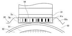
- the area Sp of the gripping surface 41 a facing the peripheral edge of the wafer 90 in the clamp part 41 is set larger than the area Sc of the barcode 94.
- the clamp portion 41 is disposed at the center in the width direction with respect to a region (identification region Rs) where the identification device 60 can identify the barcode 94.
- the above-mentioned “width direction” is defined as a direction (left-right direction in FIG. 3) perpendicular to the conveyance direction of the wafer 90 on a plane including the peripheral edge of the wafer 90 (that is, the upper surface of the ring frame 93).
- the width direction in the identification region Rs in which the identification device 60 scans the barcode 94 is referred to as “scanning width direction”.
- the reflected light transmitted through both ends of the clamp part 41 in the scanning width direction has the same optical path length to the sensor part 61. Accordingly, when the identification device 60 identifies the barcode 94, the distortion amount is the same at both ends of the barcode 94, and the distortion amount is biased by the clamp unit 41 in the scanning width direction with respect to the identification region Rs. It becomes smaller than the maximum amount of distortion when arranged.
- the component mounter 1 supplies the corresponding chip 91 to the wafer supply device 20, which is the component supply device 3, when it is necessary to mount a predetermined chip 91 in the execution of the electronic component mounting process. Request.
- the wafer supply apparatus 20 first transports the wafer 90 designated by the supply request from the magazine 30 to the component supply position Ps. Next, the wafer supply device 20 pushes up a predetermined chip 91 from below by the push-up device 80 so that the chip 91 can be picked up.
- the component transfer device 4 of the component mounter 1 inputs information related to the coordinate position of the chip 91 supplied at the component supply position Ps from the wafer supply device 20 and moves the suction nozzle 13 based on the information to move the chip. 91 is adsorbed.
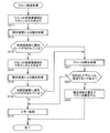
- the wafer transfer apparatus 40 executes a wafer 90 transfer process as shown in FIG.
- the ring frame 93 of the wafer 90 corresponds to the peripheral edge of the wafer 90.
- the identification code (bar code 94) including identification information used for specifying the wafer 90 is the front peripheral edge 93a in the transport direction (vertical direction in FIG. 3) or the rear of the peripheral edge (ring frame 93) of the wafer 90. It is attached to at least one of the side peripheral edge portions 93b.
- the transfer control unit 71 pulls out the wafer 90 moved to the vertical position corresponding to the slit 31a of the magazine 30 by a predetermined amount (Step 11 (hereinafter, “Step” is referred to as “S”). ))).
- Step 11 hereinafter, “Step” is referred to as “S”.
- the front peripheral edge 93a of the wafer 90 is positioned so as to be within the identification region Rs of the identification device 60 while being held by the clamp 41 (see FIG. 3).
- the clamp unit 41 maintains a state in which the front peripheral edge portion 93a of the wafer 90 is gripped.
- the identification device 60 executes identification processing of the barcode 94 attached to the wafer 90 (S12). Specifically, the identification device 60 irradiates the barcode 94 with light using an illumination LED. The irradiated light passes through the clamp part 41 and is reflected by the bar code 94, and then passes through the clamp part again. The identification device 60 receives the reflected light from the sensor unit 61 and scans the barcode 94.
- the barcode 94 When the barcode 94 is normally attached to the ring frame 93 of the wafer 90 by scanning the barcode 94, the barcode 94 is identified by the identification device 60 and the identification information is read. Subsequently, the code presence / absence determination unit 72 determines whether or not the barcode 94 is attached to the front peripheral edge portion 93a of the wafer 90 held by the clamp unit 41 based on the identification result by the identification device 60 (S13). ).
- the code presence / absence determination unit 72 determines that the barcode 94 is attached to the front peripheral edge 93a of the wafer 90 when the identification information included in the barcode 94 is read (S12). S13: Yes). On the other hand, if the identification information is not read in the identification process (S12), the code presence / absence determination unit 72 determines that the barcode 94 is not attached to the front peripheral edge 93a of the wafer 90 (S13: No).
- the transfer control unit 71 moves the clamp unit 41 in the transfer direction, and further pulls out the wafer 90 held by the clamp unit 41 (S14). Accordingly, the rear peripheral edge portion 93b of the wafer 90 is positioned so as to be within the identification region Rs of the identification device 60.
- the identification device 60 executes identification processing for the barcode 94 attached to the rear peripheral edge portion 93b (S15). Subsequently, the code presence / absence determination unit 72 determines whether or not the barcode 94 is attached to the rear peripheral edge 93b of the wafer 90 based on the result of the identification process (S15) (S16).
- the identification process (S15) for the rear peripheral edge 93b and the determination of the presence or absence of the barcode 94 (S16) are substantially the same as the identification process (S12) for the front peripheral edge 93a and the determination of the presence or absence of the barcode 94 (S13). Therefore, detailed description is omitted.
- the wafer 90 has the barcode 94 on both the front peripheral edge 93a and the rear peripheral edge 93b. Is not properly attached.
- the wafer transfer apparatus 40 executes error processing (S17) and ends the transfer process.
- the error processing (S17) includes notifying the wafer supply apparatus 20 that it is unclear whether or not the drawn wafer 90 matches the wafer specified by the supply request. For example, when the same kind of wafer 90 is stored in the wafer stocker 32, the wafer supply apparatus 20 that has input the notification may be replaced with the wafer 90. Further, if the wafer supply apparatus 20 cannot be replaced with another wafer, the wafer supply apparatus 20 notifies the component mounter 1 that the designated chip 91 cannot be supplied.
- the wafer 90 collation process is executed (S21). Specifically, the transfer control unit 71 collates the wafer 90 pulled out from the magazine 30 with the wafer designated by the supply request by the wafer supply apparatus 20 based on the identification information acquired by reading.
- the wafer transfer device 40 executes error processing (S17) and performs transfer processing. finish.
- the error processing (S17) includes notifying the wafer supply apparatus 20 that the pulled wafer 90 and the wafer specified by the supply request do not match.
- the operation of the wafer supply apparatus 20 that has input the notification is the same as the operation of the wafer supply apparatus 20 when it is determined that the barcode 94 is not attached (S16: No).
- the transfer control unit 71 controls the operation of the driving device 50 and clamps 41
- the wafer 90 held by is transferred to the component supply position Ps (S23).
- the wafer transfer apparatus 40 ends the transfer process of the wafer 90.
- the wafer transfer apparatus 40 of this embodiment takes out a predetermined wafer 90 from the magazine 30 that accommodates a plurality of wafers 90 in a stacked state, and transfers the wafer 90.
- An identification code (bar code 94) including identification information used for specifying the wafer 90 is attached to the peripheral portion of the wafer 90.
- the wafer transfer device 40 includes a clamp unit 41 that grips the peripheral edge of the wafer 90, a drive device 50 that moves the clamp unit 41 in the transfer direction of the wafer 90, and a wafer that is at least partially removed from the magazine 30.
- an identification device 60 that identifies the identification code by receiving reflected light reflected by the identification code of the wafer 90.
- the clamp portion 41 is formed of a material that transmits the reflected light reflected by the identification code, and enables the identification device 60 to identify the identification code while holding the peripheral portion of the wafer 90 to which the identification code is attached. .
- the identification device 60 can identify the barcode 94 without opening the clamp portion 41 and retracting it.
- the gripping state by the clamp unit 41 is maintained. This determination can be made. Thereby, extension of cycle time is suppressed.
- the area Sp of the gripping surface 41a facing the peripheral edge of the wafer 90 in the clamp part 41 is set larger than the area Sc of the identification code (bar code 94) (see FIG. 4).
- the bar code 94 is not separated by the end portion of the clamp portion 41 in a state where the clamp portion 41 holds the wafer 90. Thereby, the reflected light reflected by the barcode 94 passes through the clamp part 41 through an optical path corresponding to the refractive index of the clamp part 41. Therefore, the apparent shape of the barcode 94 can be visually recognized with distortion suppressed as a whole. Accordingly, the identification accuracy of the barcode 94 by the identification device 60 is improved.
- the clamp unit 41 has a width orthogonal to the conveyance direction of the wafer 90 on a plane including the peripheral portion of the wafer 90 with respect to the region (identification region Rs) where the identification device 60 can identify the identification code (bar code 94). It is arranged at the center in the direction (scanning width direction in the present embodiment). According to such a configuration, the maximum distortion amount of the barcode 94 due to the reflected light reflected by the barcode 94 passing through the clamp portion 41 in the scanning width direction is reduced. Thereby, the identification accuracy of the barcode 94 is improved.
- the identification code (bar code 94) is attached to at least one of the front peripheral edge 93a in the transfer direction and the rear peripheral edge 93b in the transfer direction among the front peripheral edge 93a of the wafer 90.
- the clamp unit 41 holds the front peripheral edge 93 a of the wafer 90.
- the wafer transfer device 40 has a determination unit (code presence / absence determination unit 72) that determines whether or not the identification code is attached to the front peripheral edge 93a gripped by the clamp unit 41 based on the identification result by the identification device 60. Further prepare. When the determination unit determines that the identification code is not attached to the front peripheral edge 93a, the identification device 60 identifies the identification code attached to the rear peripheral edge 93b.
- the material of the clamp part 41 is acrylic resin or glass. According to such a configuration, the clamp part 41 reliably transmits visible light. Moreover, the clamp part 41 can be formed at low cost, and the manufacturing cost can be reduced. Further, it is easy to form with a uniform density, and the clamp portion 41 with a small distortion can be formed.
- the wafer 90 is configured such that a ring frame 93 holds an adhesive sheet 92 to which a plurality of chips 91 are attached.
- the wafer transfer device 40 if a plurality of wafers are stored in the magazine 30 in a stacked state, the wafers are to be transferred by the wafer transfer device 40. Therefore, the wafer may be configured without the adhesive sheet 92 or the ring frame 93, for example. In this configuration, the identification code is attached to the peripheral edge of the wafer body.
- a barcode 94 is adopted as the identification code attached to the wafer 90.
- the identification code any of a two-dimensional code, a character string, a pattern, a color, or a combination thereof can be adopted.
- an identification code employing a two-dimensional code is configured by arranging a plurality of unit cells in a matrix shape, and includes identification information used for specifying a wafer.
- the thickness in the gripping direction (vertical direction in FIG. 2) at each part of the clamp portion 41 is set to be constant over the entire region in the scanning width direction.
- the thickness in the holding direction at each part of the clamp part 41 may be set according to the distance from each part to the sensor part 61 of the identification device 60.
- the clamp part 41 is set so that the thickness gradually increases, for example, from the center part toward both end parts.
- the upper surface of the clamp part 41 is formed to have a planar shape or a curved surface shape.
- the clamp part 41 is the other side from the edge part of the side close
- the ring frame 93 corresponding to the peripheral portion of the wafer 90 is formed of, for example, a metal material.
- the wafer 90 may employ a configuration in which the ring frame 93 is not provided as described above, or a configuration in which the ring frame 93 is formed of a flexible material having low hardness (for example, a resin material). In such a case, the peripheral portion of the wafer 90 to which the identification code is attached may be bent in the accommodated state of the wafer 90.
- the hardness of the clamp portion 41 is set higher than the hardness of the front peripheral edge portion 93 a of the wafer 90. Furthermore, the gripping surface 41a of the clamp part 41 is formed in a planar shape. According to such a configuration, the peripheral portion of the wafer 90 is stretched in a planar shape by being gripped by the clamp portion 41. Thereby, distortion of an identification code becomes small and the identification accuracy of the identification code by the identification device 60 is improved.
- the identification device 60 requires image processing when identifying the identification code and reading the identification information. Therefore, when such an identification code is attached to the wafer 90, the identification device 60 includes an image conversion unit 65, an image processing unit 66, and an information acquisition unit 67, as shown in FIG. Also good.
- the image conversion unit 65 converts the reflected light reflected by the identification code into an image.
- the image processing unit 66 corrects image distortion using a correction value set in advance based on the shape and refractive index of the clamp unit 41.
- the information acquisition unit 67 reads identification information based on the corrected image. According to such a configuration, the image processing unit 66 performs correction processing on the identification code that is distorted according to the refractive index of the clamp unit 41. Thereby, since the distortion amount assumed in advance can be reflected in the image, the identification accuracy of the identification code by the identification device 60 is improved.
- the wafer conveyance device 40 is applied to a wafer supply device 20 that is a kind of the component supply device 3 of the component mounter 1.
- the wafer transfer apparatus is applied to an apparatus that takes out a predetermined wafer from a magazine that accommodates a plurality of wafers in a stacked state, transfers the wafer, and requires identification code identification during the transfer. Can do.
- the reflected light reflected by the identification code and transmitted through the clamp portion 41 is visible light.
- the reflected light may be infrared light other than visible light, for example, as long as the sensor unit 61 of the identification device 60 can receive light.
- the clamp portion 41 is formed of a material that transmits reflected light, as in the embodiment.
- SYMBOLS 1 Component mounting machine 3: Component supply apparatus 20: Wafer supply apparatus 30: Magazine 40: Wafer transfer apparatus, 41: Clamp part, 41a: Holding surface 50: Drive apparatus 60: Identification apparatus, 61: Sensor part 65: Image Conversion unit 66: Image processing unit 67: Information acquisition unit 70: Control device 72: Code presence / absence determination unit (determination unit) 90: Wafer 93: Ring frame, 93a: Front peripheral edge, 93b: Rear peripheral edge 94: Bar code (identification code) Rs: identification area, Bd: circuit board, Ps: component supply position
Landscapes
- Engineering & Computer Science (AREA)
- Manufacturing & Machinery (AREA)
- Microelectronics & Electronic Packaging (AREA)
- Container, Conveyance, Adherence, Positioning, Of Wafer (AREA)
Abstract
クランプ部がウエハを把持した状態において、識別装置による識別コードの識別を可能とするウエハ搬送装置を提供することを目的とする。 ウエハ搬送装置は、ウエハの周縁部を把持するクランプ部と、クランプ部をウエハの搬送方向に移動させる駆動装置と、当該ウエハの識別コードで反射された反射光を受光することにより当該識別コードを識別する識別装置とを備える。ウエハ搬送装置のクランプ部は、識別コードで反射された反射光を透過する材料により形成され、ウエハのうち識別コードが付された周縁部を把持した状態で識別装置による識別コードの識別を可能とする。
Description
本発明は、複数のウエハを積層させた状態で収容するマガジンから所定のウエハを取り出して搬送するウエハ搬送装置に関する。
ウエハ搬送装置は、特許文献1に示されるように、例えば部品実装機の部品供給装置の一種としてウエハを供給する装置に適用される。ウエハ搬送装置は、部品供給装置に対して所定のウエハを供給するように要求があった場合に、当該ウエハをマガジンから引き出して、部品実装機がウエハのカット部品(チップ)をピックアップ可能な部品供給位置まで搬送する。
部品供給装置は、マガジンの各スロットにどのウエハが収容されているかについて、例えばマガジン用の設定ファイルに基づいて把握する。部品供給装置は、供給要求により指定されたウエハが対応するスロットから引き出されるようにウエハ搬送装置を制御する。また、ウエハ搬送装置においてマガジンから特定のウエハを引き出す方式としては、例えば特許文献2に示されるように、クランプ部によりウエハの周縁部を把持して移動させる方式が知られている。
ところで、上記のマガジン用の設定ファイルに記録された情報と、実際にマガジンの各スロットに収容されているウエハとが一致しない場合には、供給要求により指定されたウエハと異なるウエハが供給される。そこで、ウエハ搬送装置は、搬送処理において、各ウエハに付された固有の識別コードを識別装置により識別して、識別コードに含まれる識別情報に基づいて、搬送中のウエハが指定されたウエハか否かを判定する。
ここで、クランプ部によりウエハを把持してマガジンから引き出す方式では、ウエハの識別コードがウエハの周縁部に付されていると、当該クランプ部により識別コードが覆われて識別装置が識別コードを識別できない。このような場合には、例えば識別コードを付されたウエハの周縁部がマガジンの外部に出された状態で、クランプ部は、ウエハから一旦退避される。これにより、識別コードが露出され、識別装置は、識別コードを識別可能となる。しかしながら、このような制御を行う場合には、搬送処理における動作の増加に伴うサイクルタイムの延長が懸念される。
本発明は、このような事情に鑑みてなされたものであり、クランプ部がウエハを把持した状態において、識別装置による識別コードの識別を可能とするウエハ搬送装置を提供することを目的とする。
請求項1に係るウエハ搬送装置は、複数のウエハを積層させた状態で収容するマガジンから所定の前記ウエハを取り出して搬送する。前記ウエハの周縁部には、当該ウエハの特定に用いられる識別情報を含む識別コードが付される。前記ウエハ搬送装置は、前記ウエハの前記周縁部を把持するクランプ部と、前記クランプ部を前記ウエハの搬送方向に移動させる駆動装置と、前記マガジンから少なくとも一部が取り出された状態にある前記ウエハを対象として、当該ウエハの前記識別コードで反射された反射光を受光することにより当該識別コードを識別する識別装置と、を備える。前記クランプ部は、前記識別コードで反射された前記反射光を透過する材料により形成され、前記ウエハのうち前記識別コードが付された前記周縁部を把持した状態で前記識別装置による前記識別コードの識別を可能とする。
このような構成によると、クランプ部がウエハの周縁部に付された識別コードを覆うようにウエハを把持した場合に、当該クランプ部を識別コードで反射された反射光が透過する。よって、識別コードがクランプ部に覆われた状態において、クランプ部を一旦開放して退避させることなく、識別装置は、識別コードを識別可能となる。
以下、本発明のウエハ搬送装置を具体化した実施形態について図面を参照して説明する。実施形態において、部品供給装置の一種としてウエハを供給するウエハ供給装置に、ウエハ搬送装置が適用された構成を例示する。部品供給装置は、回路基板に電子部品を実装する部品実装機の要求に応じて、部品実装機が所定の電子部品をピックアップ可能に供給する。
<実施形態>
(部品実装機1の全体構成)
部品実装機1の構成について、図1および図3を参照して説明する。部品実装機1は、図1に示すように、基板搬送装置2と、部品供給装置3と、部品移載装置4とを備える。以下の説明において、部品実装機1の水平幅方向(図1の左上から右下に向かう方向)をX軸方向とし、部品実装機1の水平長手方向(図1の右上から左下に向かう方向)をY軸方向とし、X軸およびY軸に垂直な鉛直方向(図1の上下方向)をZ軸方向とする。
(部品実装機1の全体構成)
部品実装機1の構成について、図1および図3を参照して説明する。部品実装機1は、図1に示すように、基板搬送装置2と、部品供給装置3と、部品移載装置4とを備える。以下の説明において、部品実装機1の水平幅方向(図1の左上から右下に向かう方向)をX軸方向とし、部品実装機1の水平長手方向(図1の右上から左下に向かう方向)をY軸方向とし、X軸およびY軸に垂直な鉛直方向(図1の上下方向)をZ軸方向とする。
基板搬送装置2は、ベルトコンベアなどにより構成され、回路基板Bdを搬送方向(X軸方向)へと順次搬送する。基板搬送装置2は、部品実装機1の機内における所定の位置に回路基板Bdを位置決めする。そして、基板搬送装置2は、部品実装機1による実装処理が実行された後に、回路基板Bdを部品実装機1の機外に搬出する。
部品供給装置3は、回路基板Bdに装着される電子部品を供給する。本実施形態において、上記の電子部品には、キャリアテープに所定ピッチで収容された電子部品と、ウエハ90を部品単位でカットしたチップ91とが含まれる。キャリアテープは、部品供給装置3の複数のスロットに着脱可能にセットされたフィーダにより送り移動される。これにより、部品供給装置3は、フィーダの先端側の取出し部において電子部品を供給する。また、部品実装機1は、部品供給装置3の一種としてウエハ90のチップ91を供給するウエハ供給装置20を備える。ウエハ供給装置20の詳細構成については後述する。
ここで、上記のウエハ90は、図3に示すように、複数のチップ91と、粘着シート92と、リングフレーム93と、バーコード94(本発明の「識別コード」に相当する)とを有する。複数のチップ91は、例えばウエハ本体において格子状に多数形成され、粘着シート92に貼着された状態でレーザーカッタなどにより部品単位にカットされて形成される。
リングフレーム93は、環状に形成されたプレート部材である。リングフレーム93は、放射方向に拡大された状態の粘着シート92を保持する。これにより、複数のチップ91は、リングフレーム93の開口部において互いに分離した状態となる。このような構成により、ウエハ90は、全体形状としてはプレート状からなり、外枠として機能するリングフレーム93により全体形状が保持されている。
また、ウエハ90の周縁部(本実施形態においては、リングフレーム93)には、当該ウエハ90の特定に用いられる識別コードが付される。識別コードとしては、バーコードや二次元コード、文字列、模様、色彩またはこれらの結合体の何れでも採用し得る。本実施形態において、識別コードは、図3に示すように、線幅および線同士の間隔が異なる複数の棒線を平行に配置して構成されるバーコード94を採用する。
部品移載装置4は、X軸方向およびY軸方向に移動可能に構成される。部品移載装置4は、部品実装機1の長手方向の後部側(図1の右上側)から前部側の部品供給装置3の上方にかけて配置されている。部品移載装置4は、ヘッド駆動装置11および実装ヘッド12を備える。ヘッド駆動装置11は、直動機構により移動台をXY軸方向に移動可能に構成されている。実装ヘッド12は、ヘッド駆動装置11の移動台に着脱可能に設けられている。
また、実装ヘッド12には、複数の吸着ノズル13が着脱可能に設けられる。実装ヘッド12は、Z軸と平行なR軸回りに回転可能に、且つ昇降可能に各吸着ノズル13を支持する。各吸着ノズル13は、実装ヘッド12に対する昇降位置や角度、負圧の供給状態を制御される。各吸着ノズル13は、負圧を供給されることにより、フィーダの取出し部において供給される電子部品、およびウエハ供給装置20により供給されたウエハ90のチップ91を吸着して保持する。
(ウエハ供給装置20の詳細構成)
ウエハ供給装置20は、図2および図5に示すように、記憶装置21と、マガジン30と、ウエハ搬送装置40と、突き上げ装置80とを備える。記憶装置21は、マガジン30の各スロットにどのウエハ90が収容されているかが記録されたマガジン用の設定ファイルなどを記憶する。
ウエハ供給装置20は、図2および図5に示すように、記憶装置21と、マガジン30と、ウエハ搬送装置40と、突き上げ装置80とを備える。記憶装置21は、マガジン30の各スロットにどのウエハ90が収容されているかが記録されたマガジン用の設定ファイルなどを記憶する。
マガジン30は、ハウジング31と、ウエハストッカ32と、ストッカ昇降装置33とを備える。ハウジング31は、直方体状に形成される。ハウジング31は、外周面のうち部品移載装置4が電子部品をピックアップする部品供給位置Psに面する部位に、ウエハ90を搬入および搬出可能なスリット31aが形成される。
ウエハストッカ32は、ハウジング31の内部に昇降可能に設けられる。ウエハストッカ32は、複数のウエハ90を積層させた状態で収容する。より詳細には、ウエハストッカ32は、Z軸方向に等間隔に配置された複数のスロットが形成されており、各スロットにウエハ90がY軸方向に摺動可能に収容される。
ストッカ昇降装置33は、ハウジング31の内部においてウエハストッカ32を昇降可能に配置される。ストッカ昇降装置33は、ハウジング31に対して昇降可能に設けられたウエハストッカ32を支持する。ストッカ昇降装置33は、例えばモータとボールねじ機構により構成され、ハウジング31に対してウエハストッカ32を所定の上下方向位置に昇降させる。
このような構成により、マガジン30は、制御指令に基づいてウエハストッカ32を昇降させ、所定のウエハ90をハウジング31のスリット31aから搬出可能とする。同様に、マガジン30は、ウエハストッカ32の空きスロットをハウジング31のスリット31aに対応する上下方向位置に位置決めすることにより、当該空きスロットにウエハ90を搬入可能とする。
ウエハ搬送装置40は、マガジン30から所定のウエハ90を取り出して搬送する。ウエハ搬送装置40は、図2、図3、および図5に示すように、クランプ部41と、アーム42と、ウエハテーブル43と、駆動装置50と、識別装置60と、制御装置70とを備える。クランプ部41は、ウエハストッカ32に収容された複数のウエハ90のうち、ハウジング31のスリット31aに対応する上下方向位置にあるウエハ90の前側周縁部93aを把持可能に構成される。クランプ部41の詳細構成については後述する。
アーム42の基端部は、駆動装置50に固定される。アーム42の先端部は、クランプ部41を支持する。ウエハテーブル43は、部品移載装置4が電子部品(チップ91)をピックアップ可能な部品供給位置Psに配置される。ウエハテーブル43は、上方に搬送されたウエハ90のリングフレーム93を保持可能に構成される。
駆動装置50は、アーム42を介してクランプ部41を搬送方向(図2の左右方向)に移動させるローダである。また、駆動装置50は、クランプ部41に設けられたアクチュエータ(図示しない)を作動させて、クランプ部41の把持状態と開放状態を切り換える。駆動装置50は、スライド本体51と、ガイドレール52と、無端ベルト53と、サーボモータ54とを有する。
駆動装置50のスライド本体51は、アーム42の基端部を支持する。スライド本体51は、Y軸方向に延びるガイドレール52によって、搬送方向に沿って移動可能に案内される。また、スライド本体51は、無端ベルト53の一部に固定される。無端ベルト53は、一対のプーリ(図示しない)に懸架され、一方のプーリの回転軸に連結されたサーボモータ54の駆動により回転する。
このような構成により、駆動装置50は、制御指令に基づいてサーボモータ54を駆動させて、無端ベルト53、スライド本体51、およびアーム42を介してクランプ部41を搬送方向に往復移動させる。駆動装置50は、上記の搬送動作に加えて、クランプ部41の把持状態と開放状態を切り換える把持動作を同期させて、マガジン30から引き出したウエハ90をウエハテーブル43まで搬出し、またウエハテーブル43からマガジン30にウエハ90を搬入する。
識別装置60は、マガジン30から少なくとも一部が取り出された状態にあるウエハ90を対象として、当該ウエハ90のバーコード94で反射された反射光を受光することによりバーコード94を識別して、バーコード94に含まれる識別情報を読み取る。識別装置60は、図2に示すように、ハウジング31の外周面のうちスリット31aが形成された外周面の上部に設けられる。
識別装置60は、バーコード94で反射された反射光を受光するセンサ部61を備える。このような構成により、識別装置60は、図3に示すように、ハウジング31のスリット31aに隣接する識別領域Rsにおいて、バーコード94を識別可能としている。つまり、識別装置60は、マガジン30から一部が引き出された状態にあるウエハ90を対象として、当該ウエハ90に付されたバーコード94の識別情報を読み取る。
制御装置70は、主として、CPUや各種メモリ、制御回路により構成される。制御装置70は、インターフェース回路を介して駆動装置50および識別装置60と接続され、ウエハ搬送装置40によるウエハ90の搬送処理を制御する。制御装置70は、図5に示すように、搬送制御部71と、コード有無判定部72とを備える。搬送制御部71は、ウエハ供給装置20の制御指令に基づいて、ウエハ搬送装置40によるウエハ90の搬送処理を実行する。
具体的には、搬送制御部71は、駆動装置50の動作を制御して、クランプ部41によるウエハ90の把持および開放を切り換えるとともに、クランプ部41に把持されたウエハ90をマガジン30とウエハテーブル43との間で移動させる。また、搬送制御部71は、識別装置60の動作を制御して、マガジン30から引き出したウエハ90を特定し、このウエハ90と供給要求により指定されたウエハとを照合する。当該照合処理を含むウエハ搬送装置40による搬送処理の詳細については後述する。
コード有無判定部72は、クランプ部41が把持したウエハ90の周縁部にバーコード94が付されているか否かを判定する。より具体的には、識別装置60は、制御装置70による制御指令に基づいて、識別領域Rsに光を照射し、センサ部61により反射光を受光して識別を行う。コード有無判定部72は、この識別の結果に基づいて、識別情報が読み取られた場合にはバーコード94が付されていたものと判定し、それ以外の場合にはバーコード94が付されていなかったものと判定する。
突き上げ装置80は、図2に示すように、部品供給位置Psにおいて、ウエハ搬送装置40の下方の基台に設けられる。突き上げ装置80は、ピン昇降装置81と、ピン部材82とを備える。ピン昇降装置81は、XYロボットに支持され、部品供給位置PsにおいてX軸方向(図2の前後方向)およびY軸方向(図2の左右方向)に移動可能に設けられる。また、ピン昇降装置81は、Z軸方向に延びるピン部材82を支持する。
突き上げ装置80は、ウエハテーブル43に保持されたウエハ90における所定のXY位置にある部位を下方から突き上げる。ウエハ90のうち当該所定のXY位置にあるチップ91は、ピン部材82の突き上げによって粘着シート92から剥離される。そして、チップ91は、負圧を供給された状態にある吸着ノズル13によりピックアップされる。
このような構成からなるウエハ供給装置20は、制御指令に基づいてウエハ90の供給処理を実行する。ウエハ90の供給処理には、マガジン30によるウエハストッカ32の昇降処理、ウエハ搬送装置40によるウエハ90の搬送処理、突き上げ装置80による所定のチップ91の剥離処理などが含まれる。
(クランプ部41の詳細構成)
クランプ部41は、図2に示すように、ウエハ90の周縁部(リングフレーム93)を上下方向から挟み込むことにより、ウエハ90を把持する。クランプ部41は、識別装置60により照射した光のうちウエハ90のバーコード94で反射した反射光を透過する材料により形成される。
クランプ部41は、図2に示すように、ウエハ90の周縁部(リングフレーム93)を上下方向から挟み込むことにより、ウエハ90を把持する。クランプ部41は、識別装置60により照射した光のうちウエハ90のバーコード94で反射した反射光を透過する材料により形成される。
つまり、クランプ部41は、識別装置60が識別のために可視光を照射する場合には、当該可視光を透過可能な透明の材料により形成される。透明の材料としてはアクリル樹脂やガラスなど種々のものが適用可能である。本実施形態においては、クランプ部41は、アクリル樹脂により形成される。このような構成により、クランプ部41は、ウエハ90のうちバーコード94が付された周縁部を把持した状態で識別装置60によるバーコード94の識別を可能とする。
また、図4に示すように、クランプ部41のうちウエハ90の周縁部と対向する把持面41aの面積Spは、バーコード94の面積Scよりも大きく設定される。これにより、ウエハ90のうちバーコード94が付された周縁部をクランプ部41が把持した場合に、バーコード94の全体がクランプ部41に覆われた状態となる。このような状態では、バーコード94で反射された反射光は、全てクランプ部41を透過する。
ここで、上記のようにバーコード94が透明のクランプ部41に把持されると、透過光により視認されるバーコード94の見かけの形状は、クランプ部41の形状や屈折率などに応じて歪む。そこで、クランプ部41は、図3に示すように、識別装置60がバーコード94を識別可能な領域(識別領域Rs)に対して、幅方向の中央に配置される。上記の「幅方向」は、ウエハ90の周縁部を含む平面(即ちリングフレーム93の上面)においてウエハ90の搬送方向に直交する方向(図3の左右方向)と定義される。以下では、識別装置60がバーコード94を走査する識別領域Rsにおける上記の幅方向を「走査幅方向」と称する。
このような構成により、バーコード94で反射された反射光のうちクランプ部41の走査幅方向の両端部を透過した反射光は、センサ部61までの光路長さが同程度となる。これにより、識別装置60がバーコード94を識別する際に、バーコード94の両端部では同程度の歪み量となり、その歪み量は、識別領域Rsに対してクランプ部41が走査幅方向に偏って配置された場合の最大歪み量と比較して小さくなる。
(ウエハ搬送装置40によるウエハの搬送処理)
部品実装機1は、電子部品の実装処理の実行において、所定のチップ91の装着が必要となった場合に、部品供給装置3であるウエハ供給装置20に対して、対応するチップ91の供給を要求する。ウエハ供給装置20は、先ず、供給要求により指定されたウエハ90をマガジン30から部品供給位置Psまで搬送する。次に、ウエハ供給装置20は、突き上げ装置80により所定のチップ91を下方から突き上げて、当該チップ91をピックアップ可能な状態とする。
部品実装機1は、電子部品の実装処理の実行において、所定のチップ91の装着が必要となった場合に、部品供給装置3であるウエハ供給装置20に対して、対応するチップ91の供給を要求する。ウエハ供給装置20は、先ず、供給要求により指定されたウエハ90をマガジン30から部品供給位置Psまで搬送する。次に、ウエハ供給装置20は、突き上げ装置80により所定のチップ91を下方から突き上げて、当該チップ91をピックアップ可能な状態とする。
部品実装機1の部品移載装置4は、部品供給位置Psにおいて供給されたチップ91の座標位置に係る情報をウエハ供給装置20から入力し、当該情報に基づいて吸着ノズル13を移動させてチップ91を吸着する。このようなウエハ供給装置20によるウエハ90の供給処理において、ウエハ搬送装置40は、図6に示すように、ウエハ90の搬送処理を実行する。
ここで、ウエハ90のリングフレーム93は、ウエハ90の周縁部に相当する。また、ウエハ90の特定に用いられる識別情報を含む識別コード(バーコード94)は、ウエハ90の周縁部(リングフレーム93)のうち搬送方向(図3の上下方向)の前側周縁部93aまたは後側周縁部93bの少なくとも一方に付されるものとする。
ウエハ90の搬送処理において、先ず、搬送制御部71は、マガジン30のスリット31aに対応する上下方向位置に移動されたウエハ90を所定量だけ引き出す(ステップ11(以下、「ステップ」を「S」と表記する))。これにより、ウエハ90の前側周縁部93aは、クランプ部41に把持された状態で識別装置60の識別領域Rsの内部に収まるように位置決めされる(図3を参照)。このとき、クランプ部41は、上記のようにウエハ90がマガジン30から取り出された場合に、ウエハ90の前側周縁部93aを把持した状態を維持する。
次に、識別装置60は、ウエハ90に付されたバーコード94の識別処理を実行する(S12)。詳細には、識別装置60は、照明用のLEDにより光をバーコード94に対して照射する。照射された光は、クランプ部41を透過してバーコード94で反射され、再びクランプ部を透過する。識別装置60は、センサ部61により反射光を受光してバーコード94を走査する。
バーコード94の走査によりウエハ90のリングフレーム93にバーコード94が正常に付されている場合には、当該バーコード94は、識別装置60により識別されて、識別情報を読み取られる。続いて、コード有無判定部72は、クランプ部41が把持したウエハ90の前側周縁部93aにバーコード94が付されているか否かを、識別装置60による識別の結果に基づいて判定する(S13)。
コード有無判定部72は、識別処理(S12)において、バーコード94に含まれる識別情報が読み取られた場合には、ウエハ90の前側周縁部93aにバーコード94が付されていると判定する(S13:Yes)。一方で、コード有無判定部72は、識別処理(S12)において、識別情報が読み取られなかった場合には、ウエハ90の前側周縁部93aにバーコード94が付されていないと判定する(S13:No)。
搬送制御部71は、クランプ部41を搬送方向に移動させて、クランプ部41が把持しているウエハ90をさらに引き出す(S14)。これにより、ウエハ90の後側周縁部93bは、識別装置60の識別領域Rsの内部に収まるように位置決めされる。識別装置60は、後側周縁部93bに付されたバーコード94の識別処理を実行する(S15)。続いて、コード有無判定部72は、ウエハ90の後側周縁部93bにバーコード94が付されているか否かを、識別処理(S15)の結果に基づいて判定する(S16)。
後側周縁部93bに対する識別処理(S15)およびバーコード94の有無の判定(S16)は、前側周縁部93aに対する識別処理(S12)およびバーコード94の有無の判定(S13)と実質的に同一であるため、詳細な説明を省略する。ここで、後側周縁部93bにバーコード94が付されていないと判定された場合には(S16:No)、ウエハ90は、前側周縁部93aにも後側周縁部93bにもバーコード94が正常に付されていないなどの状態にある。
そのため、ウエハ搬送装置40は、エラー処理(S17)を実行して、搬送処理を終了する。上記のエラー処理(S17)としては、引き出したウエハ90と、供給要求により指定されたウエハとが一致するか否かが不明である旨をウエハ供給装置20に対して通知することが含まれる。当該通知を入力したウエハ供給装置20は、例えばウエハストッカ32に同種のウエハ90が収容されている場合には、当該ウエハ90で代替してもよい。また、ウエハ供給装置20は、他のウエハで代替できない場合には、指定のチップ91を供給できない旨を部品実装機1に通知する。
搬送制御部71は、ウエハ90の前側周縁部93aまたは後側周縁部93bの何れかに付されたバーコード94の識別処理(S12,S15)によって、識別情報を読み取れた場合には(S13:Yes,S16:Yes)、ウエハ90の照合処理を実行する(S21)。具体的には、搬送制御部71は、読み取りにより取得した識別情報に基づいて、マガジン30から引き出されたウエハ90と、ウエハ供給装置20が供給要求により指定されたウエハとを照合する。
続いて、マガジン30から引き出されたウエハ90が供給要求により指定されたウエハと相違する場合には(S22:No)、ウエハ搬送装置40は、エラー処理(S17)を実行して、搬送処理を終了する。上記のエラー処理(S17)としては、引き出したウエハ90と、供給要求により指定されたウエハとが不一致である旨をウエハ供給装置20に対して通知することが含まれる。当該通知を入力したウエハ供給装置20の動作については、バーコード94が付されていないと判定された場合(S16:No)におけるウエハ供給装置20の動作と同様である。
一方で、マガジン30から引き出されたウエハ90が供給要求により指定されたウエハと一致する場合には(S22:Yes)、搬送制御部71は、駆動装置50の動作を制御して、クランプ部41が把持しているウエハ90を部品供給位置Psまで搬送する(S23)。以上により、ウエハ搬送装置40は、ウエハ90の搬送処理を終了する。
(実施形態の構成による効果)
本実施形態のウエハ搬送装置40は、複数のウエハ90を積層させた状態で収容するマガジン30から所定のウエハ90を取り出して搬送する。ウエハ90の周縁部には、当該ウエハ90の特定に用いられる識別情報を含む識別コード(バーコード94)が付される。
ウエハ搬送装置40は、ウエハ90の周縁部を把持するクランプ部41と、クランプ部41をウエハ90の搬送方向に移動させる駆動装置50と、マガジン30から少なくとも一部が取り出された状態にあるウエハ90を対象として、当該ウエハ90の識別コードで反射された反射光を受光することにより当該識別コードを識別する識別装置60と、を備える。
クランプ部41は、識別コードで反射された反射光を透過する材料により形成され、ウエハ90のうち識別コードが付された周縁部を把持した状態で識別装置60による識別コードの識別を可能とする。
本実施形態のウエハ搬送装置40は、複数のウエハ90を積層させた状態で収容するマガジン30から所定のウエハ90を取り出して搬送する。ウエハ90の周縁部には、当該ウエハ90の特定に用いられる識別情報を含む識別コード(バーコード94)が付される。
ウエハ搬送装置40は、ウエハ90の周縁部を把持するクランプ部41と、クランプ部41をウエハ90の搬送方向に移動させる駆動装置50と、マガジン30から少なくとも一部が取り出された状態にあるウエハ90を対象として、当該ウエハ90の識別コードで反射された反射光を受光することにより当該識別コードを識別する識別装置60と、を備える。
クランプ部41は、識別コードで反射された反射光を透過する材料により形成され、ウエハ90のうち識別コードが付された周縁部を把持した状態で識別装置60による識別コードの識別を可能とする。
このような構成によると、クランプ部41がウエハ90の周縁部に付されたバーコード94を覆うようにウエハ90を把持した場合に、当該クランプ部41をバーコード94で反射された反射光が透過する。よって、バーコード94がクランプ部41に覆われた状態において、クランプ部41を一旦開放して退避させることなく、識別装置60は、バーコード94を識別可能となる。
従って、ウエハ90の搬送処理において、マガジン30から引き出されたウエハ90が、供給要求により指定されたウエハ90か否かを判定する場合に(S21,S22)、クランプ部41による把持状態を維持して当該判定をすることができる。これにより、サイクルタイムの延長が抑制される。
また、クランプ部41のうちウエハ90の周縁部と対向する把持面41aの面積Spは、識別コード(バーコード94)の面積Scよりも大きく設定される(図4を参照)。ウエハ90のうち識別コードが付された周縁部をクランプ部41が把持した場合に、識別コードの全体がクランプ部41に覆われた状態とされる。
このような構成によると、クランプ部41がウエハ90を把持した状態において、バーコード94がクランプ部41の端部により区切られない。これにより、バーコード94で反射した反射光は、クランプ部41の屈折率に応じた光路でクランプ部41を透過する。よって、バーコード94の見かけの形状は、全体として歪みが抑制された状態で視認可能となる。従って、識別装置60によるバーコード94の識別精度が向上する。
また、クランプ部41は、識別装置60が識別コード(バーコード94)を識別可能な領域(識別領域Rs)に対して、ウエハ90の周縁部を含む平面においてウエハ90の搬送方向に直交する幅方向(本実施形態の走査幅方向)の中央に配置される。
このような構成によると、走査幅方向において、バーコード94で反射した反射光がクランプ部41を透過することによるバーコード94の最大歪み量が小さくなる。これにより、バーコード94の識別精度が向上する。
このような構成によると、走査幅方向において、バーコード94で反射した反射光がクランプ部41を透過することによるバーコード94の最大歪み量が小さくなる。これにより、バーコード94の識別精度が向上する。
また、識別コード(バーコード94)は、ウエハ90の前側周縁部93aのうち搬送方向の前側周縁部93aおよび搬送方向の後側周縁部93bの少なくとも一方に付される。クランプ部41は、ウエハ90がマガジン30から取り出される場合に当該ウエハ90の前側周縁部93aを把持する。
ウエハ搬送装置40は、クランプ部41が把持した前側周縁部93aに識別コードが付されているか否かを、識別装置60による識別の結果に基づいて判定する判定部(コード有無判定部72)をさらに備える。
識別装置60は、判定部により前側周縁部93aに識別コードが付されていないと判定された場合に、後側周縁部93bに付された識別コードを識別する。
ウエハ搬送装置40は、クランプ部41が把持した前側周縁部93aに識別コードが付されているか否かを、識別装置60による識別の結果に基づいて判定する判定部(コード有無判定部72)をさらに備える。
識別装置60は、判定部により前側周縁部93aに識別コードが付されていないと判定された場合に、後側周縁部93bに付された識別コードを識別する。
このような構成によると、クランプ部41がウエハ90の前側周縁部93aを把持した状態でバーコード94の有無を判定することが可能となる(S13)。そして、前側周縁部93aにバーコード94が付されていない場合にのみ後側周縁部93bを識別領域Rsまで移動させるようにウエハ90を搬送するので、搬送処理におけるウエハ90の照合処理などの効率を向上できる。
また、クランプ部41の材料は、アクリル樹脂またはガラスである。
このような構成によると、クランプ部41は、確実に可視光を透過させる。また、クランプ部41を安価に形成することが可能であり、製造コストを低減できる。また、均一な密度での形成が容易であり、歪みの小さなクランプ部41を形成することができる。
このような構成によると、クランプ部41は、確実に可視光を透過させる。また、クランプ部41を安価に形成することが可能であり、製造コストを低減できる。また、均一な密度での形成が容易であり、歪みの小さなクランプ部41を形成することができる。
<実施形態の変形態様>
(ウエハについて)
実施形態において、ウエハ90は、複数のチップ91が貼着された粘着シート92を、リングフレーム93が保持して構成される。これに対して、ウエハは、マガジン30に積層された状態で複数収容されるものであれば、ウエハ搬送装置40の搬送対象となる。よって、ウエハは、例えば粘着シート92やリングフレーム93を有しない構成としてもよい。当該構成において、識別コードは、ウエハ本体の周縁部に付される。
(ウエハについて)
実施形態において、ウエハ90は、複数のチップ91が貼着された粘着シート92を、リングフレーム93が保持して構成される。これに対して、ウエハは、マガジン30に積層された状態で複数収容されるものであれば、ウエハ搬送装置40の搬送対象となる。よって、ウエハは、例えば粘着シート92やリングフレーム93を有しない構成としてもよい。当該構成において、識別コードは、ウエハ本体の周縁部に付される。
また、実施形態において、ウエハ90に付される識別コードは、バーコード94を採用する。これに対して、識別コードとしては、二次元コード、文字列、模様、色彩またはこれらの結合体の何れでも採用し得る。例えば、二次元コードを採用する識別コードは、複数の単位セルをマトリックス形状に配列されて構成され、ウエハの特定に用いられる識別情報を含む。
(クランプ部について)
実施形態において、クランプ部41の各部位における把持方向(図2の上下方向)の厚みは、走査幅方向の全域に亘って一定となるように設定される。これに対して、クランプ部41の各部位における把持方向の厚みは、各部位から識別装置60のセンサ部61までの距離に応じて設定される構成としてもよい。
実施形態において、クランプ部41の各部位における把持方向(図2の上下方向)の厚みは、走査幅方向の全域に亘って一定となるように設定される。これに対して、クランプ部41の各部位における把持方向の厚みは、各部位から識別装置60のセンサ部61までの距離に応じて設定される構成としてもよい。
具体的には、クランプ部41は、例えば、中央部から両端部側に向かうに従って、徐々に厚みが増すように設定される。このとき、クランプ部41の上面は、平面状または曲面状をなすように形成される。また、識別装置60のセンサ部61に対してクランプ部41が走査幅方向の中央に配置されていない場合には、クランプ部41は、例えば、センサ部61に近接する側の端部から他方側の端部に向かうに従って、徐々に厚みが増すように設定される。このような構成によると、例えば歪み量を補正するようにクランプ部41の把持方向の厚みが設定されることにより、視認される識別コードの歪み量が調整される。これにより、識別装置60は、好適に識別コードを識別可能となり、確実に識別情報を読み取ることができる。
また、実施形態において、ウエハ90の周縁部に相当するリングフレーム93は、例えば金属の材料により形成される。これに対して、ウエハ90は、上述したようにリングフレーム93を有しない構成、またはリングフレーム93が可撓性を有する硬度の低い材料(例えば樹脂材料)により形成される構成を採用し得る。このような場合には、ウエハ90の収容状態において、識別コードが付されるウエハ90の周縁部が撓んでいることがある。
そこで、以下のような構成を採用してもよい。即ち、クランプ部41の硬度は、ウエハ90の前側周縁部93aの硬度よりも高く設定される。さらに、クランプ部41の把持面41aは、平面状に形成される。このような構成によると、ウエハ90の周縁部は、クランプ部41に把持されることによって、平面状に伸ばされた状態となる。これにより、識別コードの歪みが小さくなり、識別装置60による識別コードの識別精度が向上する。
(制御装置70について)
上述したように、識別コードとしては、例えば二次元コードなどを採用し得る。このような場合には、識別装置60は、識別コードを識別し識別情報を読み取る際に、画像処理を必要とする。そこで、このような識別コードがウエハ90に付される場合に、識別装置60は、図5に示すように、画像変換部65と、画像処理部66と、情報取得部67とを備える構成としてもよい。
上述したように、識別コードとしては、例えば二次元コードなどを採用し得る。このような場合には、識別装置60は、識別コードを識別し識別情報を読み取る際に、画像処理を必要とする。そこで、このような識別コードがウエハ90に付される場合に、識別装置60は、図5に示すように、画像変換部65と、画像処理部66と、情報取得部67とを備える構成としてもよい。
画像変換部65は、識別コードで反射された反射光を画像に変換する。画像処理部66は、クランプ部41の形状および屈折率に基づいて予め設定されている補正値を用いて画像の歪みを補正する。情報取得部67は、補正後の画像に基づいて識別情報を読み取る。このような構成によると、画像処理部66は、クランプ部41の屈折率に応じて歪む識別コードについて補正処理を実行する。これにより、予め想定される歪み量を画像に反映させることができるので、識別装置60による識別コードの識別精度が向上する。
(その他)
実施形態において、ウエハ搬送装置40は、部品実装機1の部品供給装置3の一種であるウエハ供給装置20に適用される。これに対して、ウエハ搬送装置は、複数のウエハを積層させた状態で収容するマガジンから所定のウエハを取り出して搬送し、当該搬送の途中で識別コードの識別を必要とする装置に適用することができる。
実施形態において、ウエハ搬送装置40は、部品実装機1の部品供給装置3の一種であるウエハ供給装置20に適用される。これに対して、ウエハ搬送装置は、複数のウエハを積層させた状態で収容するマガジンから所定のウエハを取り出して搬送し、当該搬送の途中で識別コードの識別を必要とする装置に適用することができる。
また、実施形態において、識別コードで反射されクランプ部41を透過する反射光は、可視光である。これに対して、反射光は、識別装置60のセンサ部61が受光可能であれば可視光以外の例えば赤外線としてもよい。このような構成において、クランプ部41は、実施形態と同様に、反射光を透過する材料により形成される。
1:部品実装機、 3:部品供給装置
20:ウエハ供給装置
30:マガジン
40:ウエハ搬送装置、 41:クランプ部、 41a:把持面
50:駆動装置
60:識別装置、 61:センサ部
65:画像変換部、 66:画像処理部、 67:情報取得部
70:制御装置、 72:コード有無判定部(判定部)
90:ウエハ
93:リングフレーム、 93a:前側周縁部、 93b:後側周縁部
94:バーコード(識別コード)
Rs:識別領域、 Bd:回路基板、 Ps:部品供給位置
20:ウエハ供給装置
30:マガジン
40:ウエハ搬送装置、 41:クランプ部、 41a:把持面
50:駆動装置
60:識別装置、 61:センサ部
65:画像変換部、 66:画像処理部、 67:情報取得部
70:制御装置、 72:コード有無判定部(判定部)
90:ウエハ
93:リングフレーム、 93a:前側周縁部、 93b:後側周縁部
94:バーコード(識別コード)
Rs:識別領域、 Bd:回路基板、 Ps:部品供給位置
Claims (8)
- 複数のウエハを積層させた状態で収容するマガジンから所定の前記ウエハを取り出して搬送するウエハ搬送装置であって、
前記ウエハの周縁部には、当該ウエハの特定に用いられる識別情報を含む識別コードが付され、
前記ウエハ搬送装置は、
前記ウエハの前記周縁部を把持するクランプ部と、
前記クランプ部を前記ウエハの搬送方向に移動させる駆動装置と、
前記マガジンから少なくとも一部が取り出された状態にある前記ウエハを対象として、当該ウエハの前記識別コードで反射された反射光を受光することにより当該識別コードを識別する識別装置と、を備え、
前記クランプ部は、前記識別コードで反射された前記反射光を透過する材料により形成され、前記ウエハのうち前記識別コードが付された前記周縁部を把持した状態で前記識別装置による前記識別コードの識別を可能とするウエハ搬送装置。 - 前記クランプ部のうち前記ウエハの前記周縁部と対向する把持面の面積は、前記識別コードの面積よりも大きく設定され、
前記ウエハのうち前記識別コードが付された前記周縁部を前記クランプ部が把持した場合に、前記識別コードの全体が前記クランプ部に覆われた状態とされる、請求項1に記載のウエハ搬送装置。 - 前記クランプ部は、前記識別装置が前記識別コードを識別可能な領域に対して、前記ウエハの前記周縁部を含む平面において前記ウエハの搬送方向に直交する幅方向の中央に配置される、請求項1または2に記載のウエハ搬送装置。
- 前記識別装置は、前記識別コードで反射された前記反射光を受光するセンサ部を有し、
前記クランプ部の各部位における把持方向の厚みは、前記各部位から前記識別装置の前記センサ部までの距離に応じて設定される、請求項1~3の何れか一項に記載のウエハ搬送装置。 - 前記識別コードは、前記ウエハの前記周縁部のうち搬送方向の前側周縁部および搬送方向の後側周縁部の少なくとも一方に付され、
前記クランプ部は、前記ウエハが前記マガジンから取り出される場合に当該ウエハの前記前側周縁部を把持し、
前記ウエハ搬送装置は、前記クランプ部が把持した前記前側周縁部に前記識別コードが付されているか否かを、前記識別装置による識別の結果に基づいて判定する判定部をさらに備え、
前記識別装置は、前記判定部により前記前側周縁部に前記識別コードが付されていないと判定された場合に、前記後側周縁部に付された前記識別コードを識別する、請求項1~4の何れか一項に記載のウエハ搬送装置。 - 前記識別装置は、
前記識別コードで反射された前記反射光を画像に変換する画像変換部と、
前記クランプ部の形状および屈折率に基づいて予め設定されている補正値を用いて前記画像の歪みを補正する画像処理部と、
補正後の前記画像に基づいて前記識別情報を取得する情報取得部と、
を有する請求項1~5の何れか一項に記載のウエハ搬送装置。 - 前記クランプ部の硬度は、前記ウエハの前記周縁部の硬度よりも高く設定され、
前記クランプ部のうち前記ウエハの前記周縁部と対向する把持面は、平面状に形成される、請求項1~6の何れか一項に記載のウエハ搬送装置。 - 前記クランプ部の前記材料は、アクリル樹脂またはガラスである、請求項1~7の何れか一項に記載のウエハ搬送装置。
Priority Applications (2)
| Application Number | Priority Date | Filing Date | Title |
|---|---|---|---|
| JP2016549854A JP6431081B2 (ja) | 2014-09-26 | 2014-09-26 | ウエハ搬送装置 |
| PCT/JP2014/075600 WO2016046952A1 (ja) | 2014-09-26 | 2014-09-26 | ウエハ搬送装置 |
Applications Claiming Priority (1)
| Application Number | Priority Date | Filing Date | Title |
|---|---|---|---|
| PCT/JP2014/075600 WO2016046952A1 (ja) | 2014-09-26 | 2014-09-26 | ウエハ搬送装置 |
Publications (1)
| Publication Number | Publication Date |
|---|---|
| WO2016046952A1 true WO2016046952A1 (ja) | 2016-03-31 |
Family
ID=55580511
Family Applications (1)
| Application Number | Title | Priority Date | Filing Date |
|---|---|---|---|
| PCT/JP2014/075600 Ceased WO2016046952A1 (ja) | 2014-09-26 | 2014-09-26 | ウエハ搬送装置 |
Country Status (2)
| Country | Link |
|---|---|
| JP (1) | JP6431081B2 (ja) |
| WO (1) | WO2016046952A1 (ja) |
Cited By (2)
| Publication number | Priority date | Publication date | Assignee | Title |
|---|---|---|---|---|
| JP2018137366A (ja) * | 2017-02-22 | 2018-08-30 | 不二越機械工業株式会社 | ウェーハid読取り装置 |
| CN113352222A (zh) * | 2021-07-07 | 2021-09-07 | 浙江海纳半导体有限公司 | 一种快速高效的抛光机陶瓷盘搬运装置 |
Citations (4)
| Publication number | Priority date | Publication date | Assignee | Title |
|---|---|---|---|---|
| JP2002050667A (ja) * | 2000-08-04 | 2002-02-15 | Canon Inc | 基板搬送装置、半導体製造装置および半導体デバイス製造方法 |
| JP4693696B2 (ja) * | 2006-06-05 | 2011-06-01 | 株式会社東京精密 | ワーク処理装置 |
| JP2012109319A (ja) * | 2010-11-15 | 2012-06-07 | Nikon Corp | 基板ホルダ、基板貼り合せ装置、積層半導体装置製造方法及び積層半導体装置 |
| JP2013026501A (ja) * | 2011-07-22 | 2013-02-04 | Samsung Techwin Co Ltd | 半導体製造装置及び半導体製造方法 |
-
2014
- 2014-09-26 JP JP2016549854A patent/JP6431081B2/ja active Active
- 2014-09-26 WO PCT/JP2014/075600 patent/WO2016046952A1/ja not_active Ceased
Patent Citations (4)
| Publication number | Priority date | Publication date | Assignee | Title |
|---|---|---|---|---|
| JP2002050667A (ja) * | 2000-08-04 | 2002-02-15 | Canon Inc | 基板搬送装置、半導体製造装置および半導体デバイス製造方法 |
| JP4693696B2 (ja) * | 2006-06-05 | 2011-06-01 | 株式会社東京精密 | ワーク処理装置 |
| JP2012109319A (ja) * | 2010-11-15 | 2012-06-07 | Nikon Corp | 基板ホルダ、基板貼り合せ装置、積層半導体装置製造方法及び積層半導体装置 |
| JP2013026501A (ja) * | 2011-07-22 | 2013-02-04 | Samsung Techwin Co Ltd | 半導体製造装置及び半導体製造方法 |
Cited By (2)
| Publication number | Priority date | Publication date | Assignee | Title |
|---|---|---|---|---|
| JP2018137366A (ja) * | 2017-02-22 | 2018-08-30 | 不二越機械工業株式会社 | ウェーハid読取り装置 |
| CN113352222A (zh) * | 2021-07-07 | 2021-09-07 | 浙江海纳半导体有限公司 | 一种快速高效的抛光机陶瓷盘搬运装置 |
Also Published As
| Publication number | Publication date |
|---|---|
| JP6431081B2 (ja) | 2018-11-28 |
| JPWO2016046952A1 (ja) | 2017-07-06 |
Similar Documents
| Publication | Publication Date | Title |
|---|---|---|
| JP6977020B2 (ja) | 半導体デバイスの転写方法 | |
| WO2004066701A1 (ja) | 対回路基板作業機およびそれに対する構成要素の供給方法 | |
| JP2009255214A (ja) | 加工装置 | |
| CN114072743A (zh) | 作业管理系统 | |
| WO2016088494A1 (ja) | レーザ切断システム | |
| JP6434529B2 (ja) | 部品実装機 | |
| JP2017175029A (ja) | ウエハ搬送装置 | |
| JP7441145B2 (ja) | 対基板作業機 | |
| CN105283063A (zh) | 电子部件安装装置以及电子部件安装方法 | |
| JP6431081B2 (ja) | ウエハ搬送装置 | |
| CN216250660U (zh) | 预治式晶圆载盘的置卸载装置 | |
| CN104871658B (zh) | 裸片供给装置 | |
| JP5030843B2 (ja) | 電子部品の実装装置及び実装方法 | |
| WO2015045033A1 (ja) | 部品装着装置 | |
| JP2011216614A (ja) | 部品実装装置および部品実装方法 | |
| JP2020194839A (ja) | 紫外線照射装置 | |
| JP6307278B2 (ja) | 表面実装機および位置ズレ検出方法 | |
| CN110312415B (zh) | 基板输送装置及电子部件安装装置 | |
| JP2022036251A (ja) | 切断・屈曲装置、および屈曲装置 | |
| TWM622071U (zh) | 預治式晶圓載盤之置卸載裝置 | |
| TWI850049B (zh) | 光學基板切割後自動取片機 | |
| CN115279525A (zh) | 焊料切断装置、焊料切断单元、零件安装装置及生产系统 | |
| JP6618052B2 (ja) | 電子部品実装機 | |
| JP2016082030A (ja) | 部品実装方法および部品実装装置 | |
| US10339348B2 (en) | Reading device |
Legal Events
| Date | Code | Title | Description |
|---|---|---|---|
| 121 | Ep: the epo has been informed by wipo that ep was designated in this application |
Ref document number: 14902497 Country of ref document: EP Kind code of ref document: A1 |
|
| ENP | Entry into the national phase |
Ref document number: 2016549854 Country of ref document: JP Kind code of ref document: A |
|
| NENP | Non-entry into the national phase |
Ref country code: DE |
|
| 122 | Ep: pct application non-entry in european phase |
Ref document number: 14902497 Country of ref document: EP Kind code of ref document: A1 |