WO2016046871A1 - レーザ装置 - Google Patents
レーザ装置 Download PDFInfo
- Publication number
- WO2016046871A1 WO2016046871A1 PCT/JP2014/075018 JP2014075018W WO2016046871A1 WO 2016046871 A1 WO2016046871 A1 WO 2016046871A1 JP 2014075018 W JP2014075018 W JP 2014075018W WO 2016046871 A1 WO2016046871 A1 WO 2016046871A1
- Authority
- WO
- WIPO (PCT)
- Prior art keywords
- laser
- seed light
- optical system
- light
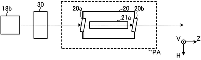
- amplifier
- Prior art date
- Legal status (The legal status is an assumption and is not a legal conclusion. Google has not performed a legal analysis and makes no representation as to the accuracy of the status listed.)
- Ceased
Links
Images






Classifications
-
- H—ELECTRICITY
- H01—ELECTRIC ELEMENTS
- H01S—DEVICES USING THE PROCESS OF LIGHT AMPLIFICATION BY STIMULATED EMISSION OF RADIATION [LASER] TO AMPLIFY OR GENERATE LIGHT; DEVICES USING STIMULATED EMISSION OF ELECTROMAGNETIC RADIATION IN WAVE RANGES OTHER THAN OPTICAL
- H01S3/00—Lasers, i.e. devices using stimulated emission of electromagnetic radiation in the infrared, visible or ultraviolet wave range
- H01S3/05—Construction or shape of optical resonators; Accommodation of active medium therein; Shape of active medium
- H01S3/08—Construction or shape of optical resonators or components thereof
- H01S3/08004—Construction or shape of optical resonators or components thereof incorporating a dispersive element, e.g. a prism for wavelength selection
-
- H—ELECTRICITY
- H01—ELECTRIC ELEMENTS
- H01S—DEVICES USING THE PROCESS OF LIGHT AMPLIFICATION BY STIMULATED EMISSION OF RADIATION [LASER] TO AMPLIFY OR GENERATE LIGHT; DEVICES USING STIMULATED EMISSION OF ELECTROMAGNETIC RADIATION IN WAVE RANGES OTHER THAN OPTICAL
- H01S3/00—Lasers, i.e. devices using stimulated emission of electromagnetic radiation in the infrared, visible or ultraviolet wave range
- H01S3/02—Constructional details
- H01S3/03—Constructional details of gas laser discharge tubes
- H01S3/034—Optical devices within, or forming part of, the tube, e.g. windows, mirrors
- H01S3/0346—Protection of windows or mirrors against deleterious effects
-
- G—PHYSICS
- G02—OPTICS
- G02B—OPTICAL ELEMENTS, SYSTEMS OR APPARATUS
- G02B27/00—Optical systems or apparatus not provided for by any of the groups G02B1/00 - G02B26/00, G02B30/00
- G02B27/28—Optical systems or apparatus not provided for by any of the groups G02B1/00 - G02B26/00, G02B30/00 for polarising
- G02B27/283—Optical systems or apparatus not provided for by any of the groups G02B1/00 - G02B26/00, G02B30/00 for polarising used for beam splitting or combining
-
- H—ELECTRICITY
- H01—ELECTRIC ELEMENTS
- H01S—DEVICES USING THE PROCESS OF LIGHT AMPLIFICATION BY STIMULATED EMISSION OF RADIATION [LASER] TO AMPLIFY OR GENERATE LIGHT; DEVICES USING STIMULATED EMISSION OF ELECTROMAGNETIC RADIATION IN WAVE RANGES OTHER THAN OPTICAL
- H01S3/00—Lasers, i.e. devices using stimulated emission of electromagnetic radiation in the infrared, visible or ultraviolet wave range
- H01S3/05—Construction or shape of optical resonators; Accommodation of active medium therein; Shape of active medium
- H01S3/08—Construction or shape of optical resonators or components thereof
- H01S3/08054—Passive cavity elements acting on the polarization, e.g. a polarizer for branching or walk-off compensation
-
- H—ELECTRICITY
- H01—ELECTRIC ELEMENTS
- H01S—DEVICES USING THE PROCESS OF LIGHT AMPLIFICATION BY STIMULATED EMISSION OF RADIATION [LASER] TO AMPLIFY OR GENERATE LIGHT; DEVICES USING STIMULATED EMISSION OF ELECTROMAGNETIC RADIATION IN WAVE RANGES OTHER THAN OPTICAL
- H01S3/00—Lasers, i.e. devices using stimulated emission of electromagnetic radiation in the infrared, visible or ultraviolet wave range
- H01S3/05—Construction or shape of optical resonators; Accommodation of active medium therein; Shape of active medium
- H01S3/08—Construction or shape of optical resonators or components thereof
- H01S3/08072—Thermal lensing or thermally induced birefringence; Compensation thereof
-
- H—ELECTRICITY
- H01—ELECTRIC ELEMENTS
- H01S—DEVICES USING THE PROCESS OF LIGHT AMPLIFICATION BY STIMULATED EMISSION OF RADIATION [LASER] TO AMPLIFY OR GENERATE LIGHT; DEVICES USING STIMULATED EMISSION OF ELECTROMAGNETIC RADIATION IN WAVE RANGES OTHER THAN OPTICAL
- H01S3/00—Lasers, i.e. devices using stimulated emission of electromagnetic radiation in the infrared, visible or ultraviolet wave range
- H01S3/09—Processes or apparatus for excitation, e.g. pumping
- H01S3/097—Processes or apparatus for excitation, e.g. pumping by gas discharge of a gas laser
- H01S3/0971—Processes or apparatus for excitation, e.g. pumping by gas discharge of a gas laser transversely excited
-
- H—ELECTRICITY
- H01—ELECTRIC ELEMENTS
- H01S—DEVICES USING THE PROCESS OF LIGHT AMPLIFICATION BY STIMULATED EMISSION OF RADIATION [LASER] TO AMPLIFY OR GENERATE LIGHT; DEVICES USING STIMULATED EMISSION OF ELECTROMAGNETIC RADIATION IN WAVE RANGES OTHER THAN OPTICAL
- H01S3/00—Lasers, i.e. devices using stimulated emission of electromagnetic radiation in the infrared, visible or ultraviolet wave range
- H01S3/10—Controlling the intensity, frequency, phase, polarisation or direction of the emitted radiation, e.g. switching, gating, modulating or demodulating
- H01S3/10084—Frequency control by seeding
- H01S3/10092—Coherent seed, e.g. injection locking
-
- H—ELECTRICITY
- H01—ELECTRIC ELEMENTS
- H01S—DEVICES USING THE PROCESS OF LIGHT AMPLIFICATION BY STIMULATED EMISSION OF RADIATION [LASER] TO AMPLIFY OR GENERATE LIGHT; DEVICES USING STIMULATED EMISSION OF ELECTROMAGNETIC RADIATION IN WAVE RANGES OTHER THAN OPTICAL
- H01S3/00—Lasers, i.e. devices using stimulated emission of electromagnetic radiation in the infrared, visible or ultraviolet wave range
- H01S3/10—Controlling the intensity, frequency, phase, polarisation or direction of the emitted radiation, e.g. switching, gating, modulating or demodulating
- H01S3/13—Stabilisation of laser output parameters, e.g. frequency or amplitude
- H01S3/1308—Stabilisation of the polarisation
-
- H—ELECTRICITY
- H01—ELECTRIC ELEMENTS
- H01S—DEVICES USING THE PROCESS OF LIGHT AMPLIFICATION BY STIMULATED EMISSION OF RADIATION [LASER] TO AMPLIFY OR GENERATE LIGHT; DEVICES USING STIMULATED EMISSION OF ELECTROMAGNETIC RADIATION IN WAVE RANGES OTHER THAN OPTICAL
- H01S3/00—Lasers, i.e. devices using stimulated emission of electromagnetic radiation in the infrared, visible or ultraviolet wave range
- H01S3/14—Lasers, i.e. devices using stimulated emission of electromagnetic radiation in the infrared, visible or ultraviolet wave range characterised by the material used as the active medium
- H01S3/22—Gases
- H01S3/223—Gases the active gas being polyatomic, i.e. containing two or more atoms
- H01S3/225—Gases the active gas being polyatomic, i.e. containing two or more atoms comprising an excimer or exciplex
-
- H—ELECTRICITY
- H01—ELECTRIC ELEMENTS
- H01S—DEVICES USING THE PROCESS OF LIGHT AMPLIFICATION BY STIMULATED EMISSION OF RADIATION [LASER] TO AMPLIFY OR GENERATE LIGHT; DEVICES USING STIMULATED EMISSION OF ELECTROMAGNETIC RADIATION IN WAVE RANGES OTHER THAN OPTICAL
- H01S3/00—Lasers, i.e. devices using stimulated emission of electromagnetic radiation in the infrared, visible or ultraviolet wave range
- H01S3/23—Arrangements of two or more lasers not provided for in groups H01S3/02 - H01S3/22, e.g. tandem arrangements of separate active media
- H01S3/2308—Amplifier arrangements, e.g. MOPA
-
- H—ELECTRICITY
- H01—ELECTRIC ELEMENTS
- H01S—DEVICES USING THE PROCESS OF LIGHT AMPLIFICATION BY STIMULATED EMISSION OF RADIATION [LASER] TO AMPLIFY OR GENERATE LIGHT; DEVICES USING STIMULATED EMISSION OF ELECTROMAGNETIC RADIATION IN WAVE RANGES OTHER THAN OPTICAL
- H01S2301/00—Functional characteristics
- H01S2301/20—Lasers with a special output beam profile or cross-section, e.g. non-Gaussian
- H01S2301/203—Lasers with a special output beam profile or cross-section, e.g. non-Gaussian with at least one hole in the intensity distribution, e.g. annular or doughnut mode
-
- H—ELECTRICITY
- H01—ELECTRIC ELEMENTS
- H01S—DEVICES USING THE PROCESS OF LIGHT AMPLIFICATION BY STIMULATED EMISSION OF RADIATION [LASER] TO AMPLIFY OR GENERATE LIGHT; DEVICES USING STIMULATED EMISSION OF ELECTROMAGNETIC RADIATION IN WAVE RANGES OTHER THAN OPTICAL
- H01S2301/00—Functional characteristics
- H01S2301/20—Lasers with a special output beam profile or cross-section, e.g. non-Gaussian
- H01S2301/206—Top hat profile
-
- H—ELECTRICITY
- H01—ELECTRIC ELEMENTS
- H01S—DEVICES USING THE PROCESS OF LIGHT AMPLIFICATION BY STIMULATED EMISSION OF RADIATION [LASER] TO AMPLIFY OR GENERATE LIGHT; DEVICES USING STIMULATED EMISSION OF ELECTROMAGNETIC RADIATION IN WAVE RANGES OTHER THAN OPTICAL
- H01S3/00—Lasers, i.e. devices using stimulated emission of electromagnetic radiation in the infrared, visible or ultraviolet wave range
- H01S3/005—Optical devices external to the laser cavity, specially adapted for lasers, e.g. for homogenisation of the beam or for manipulating laser pulses, e.g. pulse shaping
- H01S3/0071—Beam steering, e.g. whereby a mirror outside the cavity is present to change the beam direction
-
- H—ELECTRICITY
- H01—ELECTRIC ELEMENTS
- H01S—DEVICES USING THE PROCESS OF LIGHT AMPLIFICATION BY STIMULATED EMISSION OF RADIATION [LASER] TO AMPLIFY OR GENERATE LIGHT; DEVICES USING STIMULATED EMISSION OF ELECTROMAGNETIC RADIATION IN WAVE RANGES OTHER THAN OPTICAL
- H01S3/00—Lasers, i.e. devices using stimulated emission of electromagnetic radiation in the infrared, visible or ultraviolet wave range
- H01S3/05—Construction or shape of optical resonators; Accommodation of active medium therein; Shape of active medium
- H01S3/08—Construction or shape of optical resonators or components thereof
- H01S3/08004—Construction or shape of optical resonators or components thereof incorporating a dispersive element, e.g. a prism for wavelength selection
- H01S3/08009—Construction or shape of optical resonators or components thereof incorporating a dispersive element, e.g. a prism for wavelength selection using a diffraction grating
-
- H—ELECTRICITY
- H01—ELECTRIC ELEMENTS
- H01S—DEVICES USING THE PROCESS OF LIGHT AMPLIFICATION BY STIMULATED EMISSION OF RADIATION [LASER] TO AMPLIFY OR GENERATE LIGHT; DEVICES USING STIMULATED EMISSION OF ELECTROMAGNETIC RADIATION IN WAVE RANGES OTHER THAN OPTICAL
- H01S3/00—Lasers, i.e. devices using stimulated emission of electromagnetic radiation in the infrared, visible or ultraviolet wave range
- H01S3/14—Lasers, i.e. devices using stimulated emission of electromagnetic radiation in the infrared, visible or ultraviolet wave range characterised by the material used as the active medium
- H01S3/22—Gases
- H01S3/223—Gases the active gas being polyatomic, i.e. containing two or more atoms
- H01S3/225—Gases the active gas being polyatomic, i.e. containing two or more atoms comprising an excimer or exciplex
- H01S3/2251—ArF, i.e. argon fluoride is comprised for lasing around 193 nm
-
- H—ELECTRICITY
- H01—ELECTRIC ELEMENTS
- H01S—DEVICES USING THE PROCESS OF LIGHT AMPLIFICATION BY STIMULATED EMISSION OF RADIATION [LASER] TO AMPLIFY OR GENERATE LIGHT; DEVICES USING STIMULATED EMISSION OF ELECTROMAGNETIC RADIATION IN WAVE RANGES OTHER THAN OPTICAL
- H01S3/00—Lasers, i.e. devices using stimulated emission of electromagnetic radiation in the infrared, visible or ultraviolet wave range
- H01S3/14—Lasers, i.e. devices using stimulated emission of electromagnetic radiation in the infrared, visible or ultraviolet wave range characterised by the material used as the active medium
- H01S3/22—Gases
- H01S3/223—Gases the active gas being polyatomic, i.e. containing two or more atoms
- H01S3/225—Gases the active gas being polyatomic, i.e. containing two or more atoms comprising an excimer or exciplex
- H01S3/2256—KrF, i.e. krypton fluoride is comprised for lasing around 248 nm
-
- H—ELECTRICITY
- H01—ELECTRIC ELEMENTS
- H01S—DEVICES USING THE PROCESS OF LIGHT AMPLIFICATION BY STIMULATED EMISSION OF RADIATION [LASER] TO AMPLIFY OR GENERATE LIGHT; DEVICES USING STIMULATED EMISSION OF ELECTROMAGNETIC RADIATION IN WAVE RANGES OTHER THAN OPTICAL
- H01S3/00—Lasers, i.e. devices using stimulated emission of electromagnetic radiation in the infrared, visible or ultraviolet wave range
- H01S3/23—Arrangements of two or more lasers not provided for in groups H01S3/02 - H01S3/22, e.g. tandem arrangements of separate active media
- H01S3/2366—Arrangements of two or more lasers not provided for in groups H01S3/02 - H01S3/22, e.g. tandem arrangements of separate active media comprising a gas as the active medium
Definitions
- This disclosure relates to a laser device.
- the semiconductor exposure apparatus As semiconductor integrated circuits are miniaturized and highly integrated, improvement in resolving power is demanded in semiconductor exposure apparatuses.
- the semiconductor exposure apparatus is simply referred to as “exposure apparatus”. For this reason, the wavelength of light output from the light source for exposure is being shortened.
- a gas laser device As a light source for exposure, a gas laser device is used instead of a conventional mercury lamp.
- a gas laser apparatus for exposure a KrF excimer laser apparatus that outputs ultraviolet light with a wavelength of 248 nm and an ArF excimer laser apparatus that outputs ultraviolet light with a wavelength of 193 nm are used.
- the spectral line width in natural oscillation of KrF and ArF excimer laser devices is as wide as about 350 to 400 pm, the chromatic aberration of laser light (ultraviolet light) projected on the wafer by the projection lens on the exposure device side is generated, resulting in high resolution. descend. Therefore, it is necessary to narrow the spectral line width of the laser light output from the gas laser device until the chromatic aberration becomes negligible.
- the spectral line width is also called the spectral width.
- a narrow band module (Line Narrow) Module) having a narrow band element is provided in the laser resonator of the gas laser device, and the narrow band of the spectral width is realized by this narrow band module.
- the band narrowing element may be an etalon, a grating, or the like.
- Such a laser device having a narrowed spectral width is called a narrow-band laser device.
- a laser apparatus includes an oscillator that outputs seed light, a laser chamber that is disposed in an optical path of the seed light, and a pair of discharge electrodes that are disposed in the laser chamber; A conversion optical system that is disposed in the optical path of the seed light between the oscillator and the amplifier and converts the seed light so as to suppress a decrease in the polarization purity of the laser light output from the amplifier.
- FIG. 1A schematically shows a configuration of an excimer laser device according to the first embodiment.
- FIG. 1B is a schematic view of the internal configuration of the excimer laser device shown in FIG. 1A viewed from the V direction.
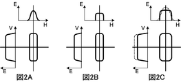
- FIG. 2A shows a beam profile of the beam cross section indicated by the line IIA-IIA in FIG. 1A.
- FIG. 2B shows the beam profile of the beam cross section indicated by the line IIB-IIB in FIG. 1A.
- FIG. 2C shows the beam profile of the beam cross section indicated by the line IIC-IIC in FIG. 1A.
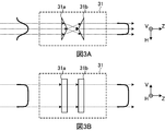
- FIG. 3A and 3B schematically show the configuration of the conversion optical system 31 used in the excimer laser device according to the second embodiment.
- 4A and 4B schematically show the configuration of the conversion optical system 32 used in the excimer laser device according to the third embodiment.
- 5A and 5B schematically show the configuration of the conversion optical system 33 used in the excimer laser device according to the fourth embodiment.
- FIG. 6 schematically shows the configuration of the conversion optical system 34 used in the excimer laser device according to the fifth embodiment.
- FIG. 7 schematically shows the configuration of the conversion optical system 35 used in the excimer laser device according to the sixth embodiment.
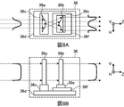
- 8A and 8B schematically show the configuration of the conversion optical system 36 used in the excimer laser device according to the seventh embodiment.
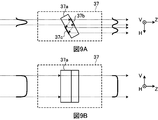
- FIG. 9A and 9B schematically show the configuration of the conversion optical system 37 used in the excimer laser device according to the eighth embodiment.
- 10A and 10B schematically show the configuration of the conversion optical system 38 used in the excimer laser device according to the ninth embodiment.
- FIG. 11A schematically shows a configuration of a conversion optical system 39 used in the excimer laser device according to the tenth embodiment.
- FIG. 11B shows an optical path in the amplifier PO when the conversion optical system 39 shown in FIG. 11A is used.
- FIG. 12 schematically shows a configuration of an amplifier PA used in the excimer laser device according to the eleventh embodiment.
- FIG. 13 schematically shows a configuration of an amplifier PO used in the excimer laser device according to the twelfth embodiment.
- the polarization purity of the output laser light may be lowered.
- the exposure performance may be adversely affected.
- the polarization purity is lowered, reflection loss may occur in a transmission optical element such as a window, and the amplification efficiency may be lowered.
- the polarization purity may be a value indicating the degree of linearly polarized light in a desired polarization direction among the light to be measured.
- the polarization purity P is defined by the following formula.
- I 1 is the light intensity of the predetermined polarization component
- I 2 is the light intensity of the polarization component orthogonal to the predetermined polarization component.
- a conversion optical system that converts seed light so as to suppress a decrease in polarization purity of laser light output from the amplifier may be disposed between the oscillator and the amplifier.
- FIG. 1A schematically shows a configuration of an excimer laser device according to the first embodiment.
- the excimer laser device shown in FIG. 1A may include an oscillator MO, an amplifier PO, high reflection mirrors 18a and 18b, and a conversion optical system 30.
- the oscillator MO may include a laser chamber 10, a pair of discharge electrodes 11 a and 11 b, a band narrowing module 14, and an output coupling mirror 15.
- the oscillator MO may be a master oscillator that oscillates and outputs seed light incident on the amplifier PO.
- FIG. 1A shows an internal configuration of the laser chamber 10 viewed from a direction substantially perpendicular to the traveling direction of the laser light inside the oscillator MO and substantially perpendicular to the discharge direction between the pair of discharge electrodes 11a and 11b.
- the traveling direction of the laser light may be the Z direction or the ⁇ Z direction.
- the discharge direction between the pair of discharge electrodes 11a and 11b may be the V direction.
- the direction perpendicular to both of these may be the H direction.
- the laser chamber 10 may be a chamber in which a laser gas as a laser medium containing, for example, argon, neon, fluorine, or the like is enclosed.
- the pair of discharge electrodes 11a and 11b may be disposed in the laser chamber 10 as electrodes for exciting the laser medium by discharge.
- a pulsed high voltage may be applied to the pair of discharge electrodes 11a and 11b from a pulse power module (not shown).
- a discharge can occur between the pair of discharge electrodes 11a and 11b. Due to the energy of this discharge, the laser medium in the laser chamber 10 can be excited to shift to a high energy level. When the excited laser medium subsequently moves to a low energy level, light corresponding to the energy level difference can be emitted.
- Windows 10 a and 10 b may be provided at both ends of the laser chamber 10. Although not shown in FIG. 1A, the windows 10a and 10b are arranged such that the light incident surfaces and the HZ planes of these windows substantially coincide with each other, and the light incident angle is substantially the Brewster angle. May be.
- the incident surface may mean a surface including an optical axis of incident light and a normal line of a boundary surface on which the light is incident.
- the light generated in the laser chamber 10 may be emitted outside the laser chamber 10 through the windows 10a and 10b.
- the band narrowing module 14 may include a prism 14a and a grating 14b.
- the prism 14a may expand the beam width in the H direction of the light emitted from the window 10a of the laser chamber 10 and make the light incident on the grating 14b.
- the prism 14a may reduce the beam width in the H direction of the reflected light from the grating 14b and transmit the light to the laser chamber 10 side.
- the prism 14a when transmitting light, the prism 14a may refract light at different angles depending on the wavelength of light. Therefore, the prism 14a can also function as a wavelength dispersion element.
- the prism 14a may be arranged such that the light incident surface with respect to the slope of the prism 14a substantially coincides with the HZ plane.
- the slope of the prism 14a may be coated with a film that suppresses reflection of p-polarized light.
- the grating 14b may be made of a highly reflective material, and a number of grooves may be formed on the surface at predetermined intervals. Each groove may be a triangular groove, for example.
- the grating 14b may be arranged in a Littrow arrangement so that the incident angle of light incident on the grating 14b from the prism 14a matches the diffraction angle of diffracted light having a desired wavelength. Thereby, the light near the desired wavelength may be returned to the laser chamber 10 via the prism 14a. Therefore, the grating 14b can function as a wavelength dispersion element.
- the narrow band module 14 for narrowing the spectral width of the laser beam may be constituted by the prism 14a and the grating 14b.
- the surface of the output coupling mirror 15 may be coated with a partial reflection film. Therefore, the output coupling mirror 15 may transmit a part of the light output from the window 10 b of the laser chamber 10 and output it, and reflect the other part and return it to the laser chamber 10.
- the band narrowing module 14 and the output coupling mirror 15 may constitute an optical resonator.
- the light emitted from the laser chamber 10 reciprocates between the band narrowing module 14 and the output coupling mirror 15, and is amplified and laser oscillated every time it passes through the laser gain space between the discharge electrodes 11a and 11b.
- the laser beam is narrowed by reciprocating between the narrowband module 14 and the output coupling mirror 15, and the polarization component in the H direction can be selected by the arrangement of the windows 10a and 10b described above.
- pulsed laser light can be output from the output coupling mirror 15 as seed light.
- the output seed light can be linearly polarized light having a polarization direction in a direction (H direction) substantially orthogonal to the discharge direction between the discharge electrodes 11a and 11b.
- High reflection mirrors 18a and 18b may be arranged so as to reflect the seed light output from the oscillator MO with high reflectance and guide it to the conversion optical system 30.
- the conversion optical system 30 may be an optical system that converts the beam profile or beam width of the seed light and outputs it to the amplifier PO. The conversion optical system 30 will be described later.
- FIG. 1B is a schematic view of a part of the internal configuration of the excimer laser device shown in FIG. 1A as viewed from the V direction.
- the amplifier PO will be described with reference to FIGS. 1A and 1B.
- the amplifier PO may include a laser chamber 20, a pair of discharge electrodes 21a and 21b, a rear mirror 24, and an output coupling mirror 25.
- the amplifier PO may include an optical resonator composed of the rear mirror 24 and the output coupling mirror 25, and a laser chamber 20 disposed in the optical resonator.
- the amplifier PO may be a power oscillator that oscillates while amplifying the seed light when the seed light is injected into the optical resonator, and outputs the laser light to an exposure apparatus (not shown) or the like.
- the configuration of the laser chamber 20, the pair of discharge electrodes 21a and 21b, and the output coupling mirror 25 may be the same as the configuration of the laser chamber 10, the pair of discharge electrodes 11a and 11b, and the output coupling mirror 15 included in the oscillator MO. .
- Windows 20 a and 20 b may be provided at both ends of the laser chamber 20. As shown in FIG. 1B, the windows 20a and 20b may be arranged such that the incident surface substantially coincides with the HZ surface and the incident angle is substantially the Brewster angle.
- the rear mirror 24 may be an element that reflects part of the laser light and transmits the other part of the laser light.
- the rear mirror 24 may be arranged so as to guide seed light incident on the rear mirror 24 via the conversion optical system 30 into the laser chamber 20.
- the rear mirror 24 transmits a part of the seed light, so that the seed light can be injected into the optical resonator constituted by the rear mirror 24 and the output coupling mirror 25.
- the reflectance of the rear mirror 24 may be 90% to 70%, and the reflectance of the output coupling mirror 25 may be 20% to 40%.
- a pulsed high voltage may be applied to the pair of discharge electrodes 21a and 21b from a pulse power module (not shown).
- the timing at which the pulsed high voltage is applied to the pair of discharge electrodes 21a and 21b may be synchronized with the timing at which the seed light is input to the amplifier PO.
- the polarization direction of the seed light incident through the conversion optical system 30 may substantially coincide with the H direction orthogonal to the discharge direction between the discharge electrodes 21a and 21b.
- the seed light may oscillate by reciprocating between the rear mirror 24 and the output coupling mirror 25.
- the amplified seed light may be output as laser light from the output coupling mirror 25.
- the polarization characteristics of the laser light output from the amplifier PO can substantially coincide with the polarization characteristics of the seed light.
- FIG. 2A shows a beam profile of the beam cross section indicated by the line IIA-IIA in FIG. 1A.
- FIG. 2B shows the beam profile of the beam cross section indicated by the line IIB-IIB in FIG. 1A.
- FIG. 2C shows the beam profile of the beam cross section indicated by the line IIC-IIC in FIG. 1A.
- the beam cross section of the seed light output from the oscillator MO may be long in the discharge direction, that is, the V direction, or may be substantially rectangular. Further, the beam profile in the V direction of the seed light output from the oscillator MO may be a substantially top hat shape having a substantially uniform energy density. The beam profile in the H direction of the seed light output from the oscillator MO may have a Gaussian distribution with a high energy density near the center and a low energy density near the end.
- the energy density near the center in the beam profile in the H direction can be further increased. If it does so, the area
- an increase in absorption of light energy near the center in the beam profile in the H direction can cause a temperature distribution in the optical element and generate thermal stress in the optical element. Due to the generation of the thermal stress, the light transmitted through the optical element is birefringent, and the linearly polarized light is converted into an elliptical change, and the polarization purity can be lowered. As a result, the imaging performance in the exposure apparatus may be deteriorated. In addition, the lifetime of the optical element may be reduced.
- the conversion optical system 30 may be, for example, an element that converts a Gaussian distribution-like beam profile in the H direction into a substantially top-hat-like beam profile.
- the energy density at the center of the beam profile can be reduced by converting the Gaussian beam profile into a substantially top-hat beam profile.
- the nonuniformity of the temperature distribution in the optical elements such as the windows 20a and 20b can be alleviated.
- the birefringence by a thermal stress can be suppressed and the fall of polarization purity can be suppressed.
- the deterioration of the imaging performance in the exposure apparatus can be suppressed.
- FIG. 2C shows the beam profile of the laser light output from the amplifier PO when the seed light having a Gaussian distribution-like beam profile in the H direction is incident on the amplifier PO without passing through the conversion optical system 30 and is amplified. This is indicated by a broken line.
- the energy density in the center of the beam profile of the laser light output from the amplifier PO can also be reduced.
- the laser beam output from the amplifier PO may have a substantially top hat beam profile in the H direction. Thereby, in the windows 20a and 20b, the nonuniformity of the temperature distribution can be relaxed, and birefringence due to thermal stress can be suppressed. As a result, a decrease in the polarization purity of the laser light output from the amplifier PO can be suppressed.
- the conversion optical system 30 is not limited to be provided between the high reflection mirror 18b and the amplifier PO, and may be provided between the high reflection mirror 18a and the high reflection mirror 18b, or between the oscillator MO and the high reflection mirror 18a. May be provided.
- Conversion optical system for converting seed light into top hat shape In the second and third embodiments described below, the beam profile in the direction orthogonal to the discharge direction between the pair of discharge electrodes 21a and 21b has a substantially top hat shape. A specific configuration of the conversion optical system that converts the seed light will be described.
- FIGS. 3A and 3B schematically show the configuration of a conversion optical system 31 used in an excimer laser device according to a second embodiment.
- 3A shows a state seen from the V direction
- FIG. 3B shows a state seen from the H direction.
- the excimer laser device according to the second embodiment may be the same as that of the first embodiment except that the conversion optical system 31 is used.
- the conversion optical system 31 may include two prisms 31a and 31b. Each of the prisms 31a and 31b may have an isosceles triangular cross section parallel to the ZH plane. The prisms 31a and 31b may be arranged so that the apex angles of the isosceles triangles of these cross sections are equal and the apexes thereof face each other.
- Seed light whose beam profile in the H direction is Gaussian may be incident on the prism 31a.
- a portion of the H-axis beam width of the seed light on the positive direction side of the H-axis is refracted and moved toward the negative direction side of the H-axis, and the negative direction of the H-axis.
- the side portion can be refracted and moved in the positive direction side of the H axis.
- the distance of this movement may be, for example, a half width at half maximum.
- FIGS. 4A and 4B schematically show the configuration of a conversion optical system 32 used in an excimer laser device according to a third embodiment.
- 4A shows a state seen from the V direction
- FIG. 4B shows a state seen from the H direction.
- the excimer laser device according to the third embodiment may be the same as that of the first embodiment except that the conversion optical system 32 is used.
- the conversion optical system 32 may include two cylindrical convex lenses 32a and 32b.
- the cylindrical convex lenses 32a and 32b may each have a plane parallel to the VH plane and a cylindrical surface having a central axis parallel to the V axis.
- Cylindrical convex lenses 32a and 32b may be arranged such that the respective cylindrical surfaces face each other and the focal positions of both cylindrical convex lenses 32a and 32b substantially coincide.
- the seed light whose beam profile in the H direction has a Gaussian distribution may be redistributed in the energy density distribution in the H direction by passing through the cylindrical convex lens 32a and may be incident on the cylindrical convex lens 32b.
- the cylindrical convex lens 32b may correct the wavefront distorted by the cylindrical convex lens 32a.
- the seed light emitted from the cylindrical convex lens 32b may be seed light having a beam divergence comparable to that of the seed light before entering the cylindrical convex lens 32a, and the beam profile may have a substantially top hat shape. As shown in FIG. 4B, the beam profile in the V direction may hardly change.
- the conversion optical system emits seed light in a direction orthogonal to the discharge direction between the pair of discharge electrodes 21a and 21b. It may be expanded.
- FIGS. 5A and 5B schematically show a configuration of a conversion optical system 33 used in an excimer laser device according to a fourth embodiment.
- 5A shows a state viewed from the V direction
- FIG. 5B shows a state viewed from the H direction.
- the excimer laser device according to the fourth embodiment may be the same as that of the first embodiment except that the conversion optical system 33 is used.
- the conversion optical system 33 may include two prisms 33a and 33b. Each of the prisms 33a and 33b may have a triangular cross section parallel to the ZH plane.
- the seed light may be incident obliquely on one surface of the prism 33a and expanded in the H direction, and further incident obliquely on one surface of the prism 33b and expanded in the H direction.
- the traveling direction of the seed light emitted from the prism 33b may be substantially the same as the traveling direction of the seed light before entering the prism 33a.
- the expansion ratio of the beam in the H direction of the seed light emitted from the prism 33b with respect to the seed light before entering the prism 33a may be 1.2 to 1.3.
- the beam profile of the seed light emitted from the prism 33b may have a Gaussian distribution similar to that of the seed light before entering the prism 33a.
- the energy density can be lowered over the entire beam profile. Therefore, the energy density at the center of the beam profile is also reduced, and the nonuniformity of the temperature distribution in the optical elements such as the windows 20a and 20b can be alleviated.
- the birefringence by a thermal stress can be suppressed and the fall of polarization purity can be suppressed. As a result, the deterioration of the imaging performance in the exposure apparatus can be suppressed.
- the beam width in the H direction of the seed light emitted from the prism 33b may be larger than the width in the H direction of the amplification region in the amplifier PO. That is, in the seed light beam expanded in the H direction, both end portions having a low energy density may not enter the amplification region of the amplifier PO.
- the optical path axis can be translated between the incident laser beam and the emitted laser beam.
- a parallel plane substrate (not shown) through which the laser beam is transmitted may be disposed.
- the parallel plane substrate may be disposed so as to be inclined such that the incident surface and the HZ plane substantially coincide with each other and the incident angle is substantially the Brewster angle.
- the beam profile and beam width in the V direction may hardly change.
- FIG. 6 schematically illustrates the configuration of a conversion optical system 34 used in an excimer laser device according to a fifth embodiment.
- FIG. 6 shows a state viewed from the V direction.
- the excimer laser device according to the fifth embodiment may be the same as that of the fourth embodiment except that the conversion optical system 34 is used.
- the conversion optical system 34 may include two wedge substrates 34a and 34b.
- the wedge substrates 34a and 34b may each have a tapered thickness.
- the seed light may be incident on one surface of the wedge substrate 34a obliquely and expanded in the H direction, and may be incident on one surface of the wedge substrate 34b obliquely and expanded in the H direction.
- the traveling direction of the seed light emitted from the wedge substrate 34b may be substantially the same as the traveling direction of the seed light before entering the wedge substrate 34a.
- the beam profile of the seed light emitted from the wedge substrate 34b may have a Gaussian distribution similar to that of the seed light before entering the wedge substrate 34a.
- the energy density can be lowered over the entire beam profile. Therefore, the energy density at the center of the beam profile is also reduced, and the nonuniformity of the temperature distribution in the optical elements such as the windows 20a and 20b can be alleviated.
- the optical path axis is shifted. Therefore, the optical path axis may be returned to its original position by inclining and arranging a parallel plane substrate (not shown).
- the beam profile and the beam width in the V direction may hardly change.
- FIG. 7 schematically shows the configuration of a conversion optical system 35 used in an excimer laser device according to a sixth embodiment.
- FIG. 7 shows a state viewed from the V direction.
- the excimer laser device according to the sixth embodiment may be the same as that of the fourth embodiment except that the conversion optical system 35 is used.
- the conversion optical system 35 may include a cylindrical concave lens 35a and a cylindrical convex lens 35b.
- the cylindrical concave lens 35a and the cylindrical convex lens 35b may each have a plane parallel to the VH plane and a cylindrical surface having a central axis parallel to the V axis.
- the focal length of the cylindrical convex lens 35b may be longer than the focal length of the cylindrical concave lens 35a.
- the cylindrical concave lens 35a and the cylindrical convex lens 35b may be arranged such that the positions of their front focal points substantially overlap each other.
- the seed light may pass through the cylindrical concave lens 35a and be expanded in the H direction.
- the beam profile of the seed light emitted from the cylindrical convex lens 35b may have a Gaussian distribution similar to that of the seed light before entering the cylindrical concave lens 35a.
- the energy density may be reduced over the entire beam profile. . Therefore, the energy density at the center of the beam profile is also reduced, and the nonuniformity of the temperature distribution in the optical elements such as the windows 20a and 20b can be alleviated.
- the beam profile and the beam width in the V direction may hardly change.
- Conversion optical system for splitting seed light into two beams In the seventh to tenth embodiments described below, the conversion optical systems are arranged in a direction orthogonal to the discharge direction between the pair of discharge electrodes 21a and 21b. The seed light may be converted into one split beam.
- FIGS. 8A and 8B schematically show a configuration of a conversion optical system 36 used in an excimer laser device according to a seventh embodiment.
- 8A shows a state seen from the V direction
- FIG. 8B shows a state seen from the H direction.
- the excimer laser device according to the seventh embodiment may be the same as that of the first embodiment except that the conversion optical system 36 is used.
- the conversion optical system 36 may include two prisms 36a and 36b. Each of the prisms 36a and 36b may have an isosceles triangle shape in cross section parallel to the ZH plane. The prisms 36a and 36b may be arranged such that the apex angles of the isosceles triangles of these cross sections are equal and the apexes thereof face each other.
- the prism 36a may be fixed by a holder 36c at a position where the seed light is incident.
- the holder 36c may be fixed to the fixed plate 36d.
- the prism 36b may be supported by the holder 36e at a position where the seed light transmitted through the prism 36a is incident.
- the holder 36e may be supported by the fixed plate 36d via the linear stage 36f.
- the linear stage 36f may support the holder 36e so that the prism 36b supported by the holder 36e can reciprocate with respect to the fixed plate 36d along the optical axis of the seed light.
- the seed light whose beam profile in the H direction is Gaussian may be incident on the prism 36a.
- a portion of the H-axis beam width of the seed light on the positive direction side of the H-axis is refracted and moved toward the negative direction side of the H-axis, and the negative direction of the H-axis.
- the side portion may be refracted and moved in the positive direction side of the H axis.
- the distance of this movement may be larger than the half width at half maximum, for example.
- the beam profile of the seed light is a beam profile having a depression with a low energy density at the center in the H direction and one energy density peak at each end. May be. Of the peaks at both ends, one peak may constitute the first split beam, and the other peak may constitute the second split beam.
- the size of the depression in the beam profile in the H direction of the seed light output from the prism 36b may be adjustable. As shown in FIG. 8B, the beam profile in the V direction may hardly change.
- the excitation at the center of the discharge in the amplifier is strong and the gain may be high. Therefore, the seed light having a depression with a low energy density at the center of the beam profile in the H direction is incident on the amplifier PO and is amplified, so that the laser light output from the amplifier PO has a beam profile close to a top hat shape. You may make it have. Thereby, the nonuniformity of the temperature distribution in the optical elements such as the windows 20a and 20b can be alleviated. As a result, birefringence due to thermal stress can be suppressed, and a decrease in polarization purity can be suppressed.
- FIGS. 9A and 9B schematically show a configuration of a conversion optical system 37 used in an excimer laser device according to an eighth embodiment.
- 9A shows a state seen from the V direction
- FIG. 9B shows a state seen from the H direction.
- the excimer laser device according to the eighth embodiment may be the same as that of the seventh embodiment except that the conversion optical system 37 is used.
- the conversion optical system 37 may include a parallel plane substrate 37a.
- the plane parallel substrate 37a may be arranged so that the incident surface of the seed light and the HZ plane substantially coincide with each other, and the incident angle is substantially the Brewster angle.
- a reflection suppressing film may be coated at the incident position of the seed light with respect to the parallel flat substrate 37a.
- a partial reflection film 37b may be coated on the first emission position of the seed light incident on the parallel flat substrate 37a.
- part of the seed light may be transmitted toward the amplifier PO as the first split beam, and the other part may be reflected toward the incident side surface of the parallel flat substrate 37a.
- a part of the incident-side surface of the parallel flat substrate 37a may be coated with a highly reflective film 37c.
- the seed light reflected by the partial reflection film 37b is reflected at a high reflectance by the high reflection film 37c and is transmitted toward the amplifier PO as a second split beam from the second emission position of the parallel flat substrate 37a.
- a reflection suppressing film (not shown) may be coated at the second emission position.
- the first split beam transmitted through the first output position and the second split beam transmitted through the second output position are substantially parallel to each other and have a peak intensity of seed light incident on the parallel plane substrate 37a. Each may have about half the peak intensity.
- Each of the first and second split beams may have a substantially Gaussian distribution in the H direction. There may be a recess having a low energy density between the first split beam and the second split beam.
- the beam profile in the V direction may hardly change.
- the excitation at the center of the discharge in the amplifier is strong and the gain may be high. Therefore, the seed light having a depression with a low energy density at the center of the beam profile in the H direction is incident on the amplifier PO and is amplified, so that the laser light output from the amplifier PO has a beam profile close to a top hat shape. You may make it have. Thereby, the nonuniformity of the temperature distribution in the optical elements such as the windows 20a and 20b is alleviated, and birefringence due to thermal stress can be suppressed.
- FIGS. 10A and 10B schematically show the configuration of a conversion optical system 38 used in an excimer laser device according to a ninth embodiment.
- FIG. 10A shows a state seen from the V direction
- FIG. 10B shows a state seen from the H direction.
- the excimer laser device according to the ninth embodiment may be the same as that of the seventh embodiment except that the conversion optical system 38 is used.
- the conversion optical system 38 may include two prisms 38a and 38b.
- the prism 38a may have a concave pentagonal cross section parallel to the ZH plane.
- the prism 38b may have an isosceles triangular cross section parallel to the ZH plane.
- the prisms 38a and 38b may have a rectangular parallelepiped shape as a whole by bringing the inclined surfaces into contact with each other with almost no gap when they are brought close to each other.
- the configuration in which the prism 38a is fixed and the prism 38b is movable may be the same as in the seventh embodiment.
- the seed light having a beam profile in the H direction having a Gaussian distribution When the seed light having a beam profile in the H direction having a Gaussian distribution is transmitted through the prism 38a, the seed light can divide into a positive direction side and a negative direction side of the H axis and be refracted and travel away from each other.
- the beam profile of the seed light By transmitting these lights through the prism 38b, the beam profile of the seed light has a depression having a low energy density at the center in the H direction and one energy density peak at each end thereof. Also good. Of the peaks at both ends, one peak may constitute the first split beam, and the other peak may constitute the second split beam. As shown in FIG. 10B, the beam profile in the V direction may hardly change.
- the excitation at the center of the discharge in the amplifier is strong and the gain may be high. Therefore, the seed light having a depression with a low energy density at the center of the beam profile in the H direction is incident on the amplifier PO and is amplified, so that the laser light output from the amplifier PO has a beam profile close to a top hat shape. You may make it have. Thereby, the nonuniformity of the temperature distribution in the optical elements such as the windows 20a and 20b is alleviated, and birefringence due to thermal stress can be suppressed.
- FIG. 11A schematically shows a configuration of a conversion optical system 39 used in an excimer laser device according to a tenth embodiment.
- FIG. 11A shows a state viewed from the V direction.
- the excimer laser device according to the tenth embodiment may be the same as that of the seventh embodiment except that the conversion optical system 39 is used.
- the conversion optical system 39 may include two prisms 39a and 39b.
- the prisms 39a and 39b may have an isosceles triangular cross section parallel to the ZH plane. However, the apex angle of the isosceles triangle may be smaller in the cross section of the prism 39b than in the cross section of the prism 39a.
- the configuration in which the prism 39a is fixed and the prism 39b can be moved may be the same as in the seventh embodiment.
- the seed light having a Gaussian beam profile in the H direction may be transmitted through the prisms 39a and 39b.
- the seed light transmitted through the prisms 39a and 39b may have a beam profile having a recess with a low energy density at the center in the H direction and one energy density peak at each end. Of the peaks at both ends, one peak may constitute the first split beam, and the other peak may constitute the second split beam.
- the first and second split beams emitted from the conversion optical system 39 may be emitted in directions closer to each other rather than in the same direction.
- the angle ⁇ between the first and second split beams and the central axis of the amplifier may be 0 mrad ⁇ ⁇ 1.5 mrad. More preferably, 0 mrad ⁇ ⁇ 1 mrad may be satisfied.
- FIG. 11B shows an optical path in the amplifier PO when the conversion optical system 39 shown in FIG. 11A is used.
- the first and second split beams split by the conversion optical system 39 may enter the window 20a at positions away from the central axis of the amplifier PO in the + H direction and the ⁇ H direction. Good.
- the first and second split beams may be amplified while approaching the central axis of the amplifier PO by reciprocating the resonator of the amplifier PO and filling the discharge region. Thereby, the nonuniformity of the temperature distribution in the optical elements such as the windows 20a and 20b is alleviated, and birefringence due to thermal stress can be suppressed.
- the configuration in which the first and second split beams are emitted from the conversion optical system in a direction approaching each other is not limited to that using a prism.
- the first and second split beams can be incident on the amplifier PO in a direction approaching each other. .
- FIG. 12 schematically shows the configuration of an amplifier PA used in an excimer laser device according to an eleventh embodiment.
- FIG. 12 shows a state viewed from the V direction.
- the excimer laser apparatus according to the eleventh embodiment may be the same as that of the first to tenth embodiments except that the amplifier PA is used.
- the amplifier PA may be different from the amplifier PO described with reference to FIG. 1A in that it does not include an optical resonator.
- the seed light that has entered the amplifier PA via the conversion optical system 30 may be amplified once through the amplification region in the laser chamber 20 and output from the amplifier PA as laser light.
- the amplifier PA may be provided with a high reflection mirror for passing the amplification region in the laser chamber 20 a plurality of times.
- the nonuniformity of the temperature distribution is reduced in the windows 20a and 20b, the birefringence is suppressed, and the polarization purity is reduced. The decrease can be suppressed.
- FIG. 13 schematically shows the configuration of an amplifier PO used in an excimer laser device according to a twelfth embodiment.
- FIG. 13 shows a state viewed from the V direction.
- the excimer laser apparatus according to the twelfth embodiment may be the same as the first to tenth embodiments except that the amplifier PO includes a ring resonator.
- the amplifier PO may include a high reflection mirror 18c, an output coupling mirror 25a, and high reflection mirrors 26a to 26c.
- the seed light incident on the amplifier PO via the conversion optical system 30 may be introduced to the output coupling mirror 25a via the high reflection mirror 18c.
- the amplifier PO may amplify the laser light so that the laser light passes through the laser chamber 20 a plurality of times by a ring-shaped optical path constituted by the high reflection mirrors 26a to 26c and the output coupling mirror 25a.
- the laser light amplified by the amplifier PO can be output as output laser light through the output coupling mirror 25a.
- the nonuniformity of the temperature distribution in the windows 20a and 20b can be alleviated and birefringence due to thermal stress can be suppressed. . As a result, a decrease in polarization purity can be suppressed.
Landscapes
- Physics & Mathematics (AREA)
- Electromagnetism (AREA)
- Optics & Photonics (AREA)
- Engineering & Computer Science (AREA)
- Plasma & Fusion (AREA)
- Lasers (AREA)
- General Physics & Mathematics (AREA)
Abstract
このレーザ装置は、シード光を出力する発振器と、シード光の光路に配置されたレーザチャンバと、レーザチャンバの中に配置された一対の放電電極と、を含む増幅器と、発振器と増幅器との間のシード光の光路に配置され、増幅器から出力されるレーザ光の偏光純度の低下を抑制するように、シード光を変換する変換光学系と、を備えてもよい。
Description
本開示は、レーザ装置に関する。
半導体集積回路の微細化、高集積化につれて、半導体露光装置においては解像力の向上が要請されている。半導体露光装置を以下、単に「露光装置」という。このため露光用光源から出力される光の短波長化が進められている。露光用光源には、従来の水銀ランプに代わってガスレーザ装置が用いられている。現在、露光用のガスレーザ装置としては、波長248nmの紫外線を出力するKrFエキシマレーザ装置ならびに、波長193nmの紫外線を出力するArFエキシマレーザ装置が用いられている。
現在の露光技術としては、露光装置側の投影レンズとウエハ間の間隙を液体で満たして、当該間隙の屈折率を変えることによって、露光用光源の見かけの波長を短波長化する液浸露光が実用化されている。ArFエキシマレーザ装置を露光用光源として用いて液浸露光が行われた場合は、ウエハには水中における波長134nmの紫外光が照射される。この技術をArF液浸露光という。ArF液浸露光はArF液浸リソグラフィーとも呼ばれる。
KrF、ArFエキシマレーザ装置の自然発振におけるスペクトル線幅は約350~400pmと広いため、露光装置側の投影レンズによってウエハ上に縮小投影されるレーザ光(紫外線光)の色収差が発生して解像力が低下する。そこで色収差が無視できる程度となるまでガスレーザ装置から出力されるレーザ光のスペクトル線幅を狭帯域化する必要がある。スペクトル線幅はスペクトル幅とも呼ばれる。このためガスレーザ装置のレーザ共振器内には狭帯域化素子を有する狭帯域化モジュール(Line Narrow Module)が設けられ、この狭帯域化モジュールによりスペクトル幅の狭帯域化が実現されている。なお、狭帯域化素子はエタロンやグレーティング等であってもよい。このようにスペクトル幅が狭帯域化されたレーザ装置を狭帯域化レーザ装置という。
本開示の1つの観点に係るレーザ装置は、シード光を出力する発振器と、シード光の光路に配置されたレーザチャンバと、レーザチャンバの中に配置された一対の放電電極と、を含む増幅器と、発振器と増幅器との間のシード光の光路に配置され、増幅器から出力されるレーザ光の偏光純度の低下を抑制するように、シード光を変換する変換光学系と、を備えてもよい。
本開示のいくつかの実施形態を、単なる例として、添付の図面を参照して以下に説明する。
図1Aは、第1の実施形態に係るエキシマレーザ装置の構成を模式的に示す。図1Bは、図1Aに示されるエキシマレーザ装置の内部構成をV方向から見た模式図である。
図2Aは、図1AにIIA-IIA線で示されるビーム断面のビームプロファイルを示す。図2Bは、図1AにIIB-IIB線で示されるビーム断面のビームプロファイルを示す。図2Cは、図1AにIIC-IIC線で示されるビーム断面のビームプロファイルを示す。
図3A及び図3Bは、第2の実施形態に係るエキシマレーザ装置において用いられる変換光学系31の構成を模式的に示す。
図4A及び図4Bは、第3の実施形態に係るエキシマレーザ装置において用いられる変換光学系32の構成を模式的に示す。
図5A及び図5Bは、第4の実施形態に係るエキシマレーザ装置において用いられる変換光学系33の構成を模式的に示す。
図6は、第5の実施形態に係るエキシマレーザ装置において用いられる変換光学系34の構成を模式的に示す。
図7は、第6の実施形態に係るエキシマレーザ装置において用いられる変換光学系35の構成を模式的に示す。
図8A及び図8Bは、第7の実施形態に係るエキシマレーザ装置において用いられる変換光学系36の構成を模式的に示す。
図9A及び図9Bは、第8の実施形態に係るエキシマレーザ装置において用いられる変換光学系37の構成を模式的に示す。
図10A及び図10Bは、第9の実施形態に係るエキシマレーザ装置において用いられる変換光学系38の構成を模式的に示す。
図11Aは、第10の実施形態に係るエキシマレーザ装置において用いられる変換光学系39の構成を模式的に示す。図11Bは、図11Aに示される変換光学系39が用いられた場合の増幅器PO内の光路を示す。
図12は、第11の実施形態に係るエキシマレーザ装置において用いられる増幅器PAの構成を模式的に示す。
図13は、第12の実施形態に係るエキシマレーザ装置において用いられる増幅器POの構成を模式的に示す。
<内容>
1.概要
2.変換光学系を有するエキシマレーザ装置(第1の実施形態)
2.1 発振器MO
2.2 高反射ミラー18a及び18b
2.3 増幅器PO
2.4 変換光学系30
3.シード光をトップハット状に変換する変換光学系
3.1 第2の実施形態
3.2 第3の実施形態
4.シード光をビームエキスパンドする変換光学系
4.1 第4の実施形態
4.2 第5の実施形態
4.3 第6の実施形態
5.シード光を2つのビームに分割する変換光学系
5.1 第7の実施形態
5.2 第8の実施形態
5.3 第9の実施形態
5.4 第10の実施形態
6.増幅器のバリエーション
6.1 第11の実施形態
6.2 第12の実施形態
1.概要
2.変換光学系を有するエキシマレーザ装置(第1の実施形態)
2.1 発振器MO
2.2 高反射ミラー18a及び18b
2.3 増幅器PO
2.4 変換光学系30
3.シード光をトップハット状に変換する変換光学系
3.1 第2の実施形態
3.2 第3の実施形態
4.シード光をビームエキスパンドする変換光学系
4.1 第4の実施形態
4.2 第5の実施形態
4.3 第6の実施形態
5.シード光を2つのビームに分割する変換光学系
5.1 第7の実施形態
5.2 第8の実施形態
5.3 第9の実施形態
5.4 第10の実施形態
6.増幅器のバリエーション
6.1 第11の実施形態
6.2 第12の実施形態
以下、本開示の実施形態について、図面を参照しながら詳しく説明する。以下に説明される実施形態は、本開示のいくつかの例を示すものであって、本開示の内容を限定するものではない。また、各実施形態で説明される構成及び動作の全てが本開示の構成及び動作として必須であるとは限らない。なお、同一の構成要素には同一の参照符号を付して、重複する説明を省略する。
1.概要
露光装置の光源として用いられるエキシマレーザ装置においては、高出力化の要求に応えるために、発振器と増幅器とを含むダブルチャンバ方式のレーザ装置が実用化されている。ダブルチャンバ方式のレーザ装置の形態としては、増幅器に共振器ミラーを設けないMOPA(Master Oscillator Power Amplifier)方式と、増幅器に共振器ミラーを設けるMOPO(Master Oscillator Power Oscillator)方式とがある。このようなエキシマレーザ装置を用いて、ダブルパターンニングやトリプルパターンニングのような多重露光も行われており、スループットを改善するためにさらなる高出力化が求められている。
露光装置の光源として用いられるエキシマレーザ装置においては、高出力化の要求に応えるために、発振器と増幅器とを含むダブルチャンバ方式のレーザ装置が実用化されている。ダブルチャンバ方式のレーザ装置の形態としては、増幅器に共振器ミラーを設けないMOPA(Master Oscillator Power Amplifier)方式と、増幅器に共振器ミラーを設けるMOPO(Master Oscillator Power Oscillator)方式とがある。このようなエキシマレーザ装置を用いて、ダブルパターンニングやトリプルパターンニングのような多重露光も行われており、スループットを改善するためにさらなる高出力化が求められている。
しかしながら、レーザ装置を高出力化すると、出力されたレーザ光の偏光純度が低下することがあり得た。偏光純度が低下すると、露光性能に悪影響を及ぼすことがあり得た。また、偏光純度が低下すると、ウインドウなどの透過光学素子において反射ロスが発生し、増幅効率が低下することがあり得た。ここで、偏光純度とは、測定対象の光のうち、所望の偏光方向の直線偏光の度合いを示す値でもよい。なお、偏光純度Pは以下の式で定義する。
P=(I1-I2)/(I1+I2)×100(%)
ここで、I1は所定の偏光成分の光強度とし、I2は上記所定の偏光成分と直交する偏光成分の光強度とする。
P=(I1-I2)/(I1+I2)×100(%)
ここで、I1は所定の偏光成分の光強度とし、I2は上記所定の偏光成分と直交する偏光成分の光強度とする。
本開示の1つの観点によれば、増幅器から出力されるレーザ光の偏光純度の低下を抑制するようにシード光を変換する変換光学系が、発振器と増幅器との間に配置されてもよい。
2.変換光学系を有するエキシマレーザ装置(第1の実施形態)
図1Aは、第1の実施形態に係るエキシマレーザ装置の構成を模式的に示す。図1Aに示されるエキシマレーザ装置は、発振器MOと、増幅器POと、高反射ミラー18a及び18bと、変換光学系30と、を含んでもよい。
図1Aは、第1の実施形態に係るエキシマレーザ装置の構成を模式的に示す。図1Aに示されるエキシマレーザ装置は、発振器MOと、増幅器POと、高反射ミラー18a及び18bと、変換光学系30と、を含んでもよい。
2.1 発振器MO
発振器MOは、レーザチャンバ10と、一対の放電電極11a及び11bと、狭帯域化モジュール14と、出力結合ミラー15と、を含んでもよい。発振器MOは、増幅器POに入射させるシード光をレーザ発振して出力するマスターオシレータであってもよい。
発振器MOは、レーザチャンバ10と、一対の放電電極11a及び11bと、狭帯域化モジュール14と、出力結合ミラー15と、を含んでもよい。発振器MOは、増幅器POに入射させるシード光をレーザ発振して出力するマスターオシレータであってもよい。
図1Aにおいては、発振器MOの内部におけるレーザ光の進行方向に略垂直で、且つ、一対の放電電極11a及び11bの間の放電方向に略垂直な方向からみたレーザチャンバ10の内部構成が示されている。図1Aにおいて、レーザ光の進行方向は、Z方向又は-Z方向であってよい。一対の放電電極11a及び11bの間の放電方向は、V方向であってよい。これらの両方に垂直な方向は、H方向であってよい。高反射ミラー18a又は18bによってレーザ光の進行方向が変化するとき、Z方向及びV方向は、当該進行方向の変化に追随して変化してもよい。
レーザチャンバ10は、例えばアルゴン、ネオン及びフッ素等を含むレーザ媒質としてのレーザガスが封入されるチャンバでもよい。一対の放電電極11a及び11bは、レーザ媒質を放電により励起するための電極として、レーザチャンバ10内に配置されてもよい。一対の放電電極11a及び11bには、図示しないパルスパワーモジュールからパルス状の高電圧が印加されてもよい。
一対の放電電極11a及び11b間に高電圧が印加されると、一対の放電電極11a及び11b間に放電が起こり得る。この放電のエネルギーにより、レーザチャンバ10内のレーザ媒質が励起されて高エネルギー準位に移行し得る。励起されたレーザ媒質が、その後低エネルギー準位に移行するとき、そのエネルギー準位差に応じた光を放出し得る。
レーザチャンバ10の両端にはウインドウ10a及び10bが設けられてもよい。図1Aには表れていないが、ウインドウ10a及び10bは、これらのウインドウに対する光の入射面とHZ平面とが略一致し、かつ、この光の入射角度が略ブリュースター角となるように配置されてもよい。入射面とは、入射する光の光軸と、この光が入射する境界面の法線とを含む面を意味してもよい。レーザチャンバ10内で発生した光は、ウインドウ10a及び10bを介してレーザチャンバ10の外部に出射してもよい。
狭帯域化モジュール14は、プリズム14aと、グレーティング14bとを含んでもよい。プリズム14aは、レーザチャンバ10のウインドウ10aから出射された光のH方向のビーム幅を拡大させて、その光をグレーティング14bに入射させてもよい。また、プリズム14aは、グレーティング14bからの反射光のH方向のビーム幅を縮小させるとともに、その光をレーザチャンバ10側に透過させてもよい。また、プリズム14aは、光を透過させるとき、光の波長に応じて異なった角度で光を屈折させてもよい。従って、プリズム14aは波長分散素子としても機能し得る。さらに、プリズム14aは、プリズム14aの斜面に対する光の入射面がHZ平面と略一致するように配置されてもよい。プリズム14aの斜面には、p偏光の反射を抑制する膜がコートされていてもよい。
グレーティング14bは、高反射率の材料によって構成され、表面に多数の溝が所定間隔で形成されていてもよい。各溝は例えば三角溝であってもよい。グレーティング14bは、プリズム14aからグレーティング14bに入射する光の入射角と、所望波長の回折光の回折角とが一致するようにリトロー配置されてもよい。これにより、所望波長付近の光がプリズム14aを介してレーザチャンバ10に戻されてもよい。従って、グレーティング14bは波長分散素子として機能し得る。
このように、プリズム14aとグレーティング14bとによって、レーザ光のスペクトル幅を狭くする狭帯域化モジュール14が構成してもよい。
出力結合ミラー15の表面には、部分反射膜がコーティングされていてもよい。従って、出力結合ミラー15は、レーザチャンバ10のウインドウ10bから出力される光のうちの一部を透過させて出力し、他の一部を反射させてレーザチャンバ10内に戻してもよい。
狭帯域化モジュール14と出力結合ミラー15とが、光共振器を構成してもよい。レーザチャンバ10から出射した光は、狭帯域化モジュール14と出力結合ミラー15との間で往復し、放電電極11a及び11bの間のレーザゲイン空間を通過する度に増幅されレーザ発振し得る。レーザ光は狭帯域化モジュール14と出力結合ミラー15との間で往復することによって狭帯域化され、上述したウインドウ10a及び10bの配置によって、H方向の偏光成分が選択され得る。その結果、パルスレーザ光が出力結合ミラー15からシード光として出力され得る。この出力されたシード光は、放電電極11a及び11bの間の放電方向と略直交する方向(H方向)に偏光方向を有する直線偏光となり得る。
2.2 高反射ミラー18a及び18b
高反射ミラー18a及び18bは、発振器MOから出力されたシード光を高い反射率で反射して、変換光学系30に導くように配置されてもよい。
変換光学系30は、シード光のビームプロファイル又はビーム幅を変換して、増幅器POに向けて出力する光学系であってもよい。変換光学系30については、後述する。
高反射ミラー18a及び18bは、発振器MOから出力されたシード光を高い反射率で反射して、変換光学系30に導くように配置されてもよい。
変換光学系30は、シード光のビームプロファイル又はビーム幅を変換して、増幅器POに向けて出力する光学系であってもよい。変換光学系30については、後述する。
2.3 増幅器PO
図1Bは、図1Aに示されるエキシマレーザ装置の内部構成の一部をV方向から見た模式図である。図1A及び図1Bを参照しながら、増幅器POについて説明する。増幅器POは、レーザチャンバ20と、一対の放電電極21a及び21bと、リアミラー24と、出力結合ミラー25と、を含んでもよい。増幅器POは、リアミラー24と出力結合ミラー25とで構成される光共振器と、この光共振器内に配置されたレーザチャンバ20と、を含んでもよい。この増幅器POは、シード光が光共振器内に注入されるとシード光を増幅しながら発振して、図示しない露光装置等に向けてレーザ光として出力するパワーオシレータであってもよい。
図1Bは、図1Aに示されるエキシマレーザ装置の内部構成の一部をV方向から見た模式図である。図1A及び図1Bを参照しながら、増幅器POについて説明する。増幅器POは、レーザチャンバ20と、一対の放電電極21a及び21bと、リアミラー24と、出力結合ミラー25と、を含んでもよい。増幅器POは、リアミラー24と出力結合ミラー25とで構成される光共振器と、この光共振器内に配置されたレーザチャンバ20と、を含んでもよい。この増幅器POは、シード光が光共振器内に注入されるとシード光を増幅しながら発振して、図示しない露光装置等に向けてレーザ光として出力するパワーオシレータであってもよい。
レーザチャンバ20、一対の放電電極21a及び21b、及び出力結合ミラー25の構成は、発振器MOに含まれるレーザチャンバ10、一対の放電電極11a及び11b、及び出力結合ミラー15の構成とそれぞれ同様でもよい。レーザチャンバ20の両端にはウインドウ20a及び20bが設けられてもよい。図1Bに示されるように、ウインドウ20a及び20bは、入射面がHZ面と略一致し、入射角度が略ブリュースター角となるように配置されてもよい。
リアミラー24は、レーザ光の一部を反射し、当該レーザ光の他の一部を透過させる素子でもよい。リアミラー24は、変換光学系30を介してリアミラー24に入射するシード光を、レーザチャンバ20内に導くように配置されてもよい。リアミラー24がシード光の一部を透過させることによって、シード光が、リアミラー24と出力結合ミラー25とによって構成されている光共振器内に注入され得る。ここで、リアミラー24の反射率は90%~70%であってもよく、出力結合ミラー25の反射率は20%~40%であってもよい。
一対の放電電極21a及び21bには、図示しないパルスパワーモジュールからパルス状の高電圧が印加されてもよい。一対の放電電極21a及び21bにパルス状の高電圧が印加されるタイミングは、シード光が増幅器POに入力されるタイミングと同期させてもよい。変換光学系30を介して入射するシード光の偏光方向は、放電電極21a及び21bの間の放電方向に対して直交するH方向と略一致していてもよい。シード光がリアミラー24と出力結合ミラー25との間で往復することによってレーザ発振してもよい。増幅されたシード光が、出力結合ミラー25からレーザ光として出力されてもよい。ここで、ウインドウ20a及び20bの複屈折の影響がなければ、増幅器POから出力されるレーザ光の偏光特性は、シード光の偏光特性と略一致し得る。
2.4 変換光学系30
図2Aは、図1AにIIA-IIA線で示されるビーム断面のビームプロファイルを示す。図2Bは、図1AにIIB-IIB線で示されるビーム断面のビームプロファイルを示す。図2Cは、図1AにIIC-IIC線で示されるビーム断面のビームプロファイルを示す。
図2Aは、図1AにIIA-IIA線で示されるビーム断面のビームプロファイルを示す。図2Bは、図1AにIIB-IIB線で示されるビーム断面のビームプロファイルを示す。図2Cは、図1AにIIC-IIC線で示されるビーム断面のビームプロファイルを示す。
図2Aに示されるように、発振器MOから出力されるシード光のビーム断面は、放電方向すなわちV方向に長い形状であってよく、ほぼ長方形状であってもよい。さらに、発振器MOから出力されるシード光のV方向のビームプロファイルは、略均一なエネルギー密度を有する略トップハット状であってもよい。また、発振器MOから出力されるシード光のH方向のビームプロファイルは、中央付近でエネルギー密度が高く、端部付近ではエネルギー密度が低いガウス分布状であってもよい。
このようなビーム断面を有するシード光を、変換光学系30を介さずに増幅器POに入射させて増幅すると、H方向のビームプロファイルにおける中央付近のエネルギー密度がさらに高くなり得る。そうすると、ウインドウ20a及び20bなどの光学素子のレーザ光が通過する領域が、光のエネルギーの吸収によって加熱され得る。特に、H方向のビームプロファイルにおける中央付近の光のエネルギーの吸収が増加することによって、光学素子に温度分布が生じ、光学素子に熱応力が発生し得る。この熱応力の発生により、光学素子を透過する光が複屈折して、直線偏光が楕円変更に変換され、偏光純度が低下し得る。その結果、露光装置における結像性能を悪化させる場合がある。また、光学素子の寿命が低下する場合がある。
そこで、図2Bに示されるように、変換光学系30は、例えば、H方向におけるガウス分布状のビームプロファイルを略トップハット状のビームプロファイルに変換する素子であってもよい。図2Aと図2Bとを比較するとわかるように、ガウス分布状のビームプロファイルを略トップハット状のビームプロファイルに変換することにより、ビームプロファイルの中央部のエネルギー密度が低減され得る。そして、H方向において略トップハット状のビームプロファイルを有するシード光を増幅器POに入射させることにより、ウインドウ20a及び20bなどの光学素子における温度分布の不均一性が緩和され得る。これにより、熱応力による複屈折が抑制され、偏光純度の低下が抑制され得る。その結果、露光装置における結像性能の悪化が抑制され得る。
H方向において略トップハット状のビームプロファイルを有するシード光を増幅器POに入射させる場合には、図2Cに実線で示されるように、増幅器POから出力されるレーザ光も、H方向において略トップハット状のビームプロファイルを有し得る。図2Cには、H方向においてガウス分布状のビームプロファイルを有するシード光を、変換光学系30を介さずに増幅器POに入射させて増幅した場合に増幅器POから出力されるレーザ光のビームプロファイルが、破線で示されている。図2Cからわかるように、変換光学系30を介してシード光を増幅器POに入射させることにより、増幅器POから出力されるレーザ光のビームプロファイルの中央部のエネルギー密度も低減され得る。そして、増幅器POから出力されるレーザ光は、H方向において略トップハット状のビームプロファイルを有し得る。これにより、ウインドウ20a及び20bにおいて、温度分布の不均一性が緩和され、熱応力による複屈折が抑制され得る。その結果、増幅器POから出力されるレーザ光の偏光純度の低下が抑制され得る。
変換光学系30は、高反射ミラー18bと増幅器POとの間に限らず、高反射ミラー18aと高反射ミラー18bとの間に設けられてもよいし、発振器MOと高反射ミラー18aとの間に設けられてもよい。
3.シード光をトップハット状に変換する変換光学系
次に述べる第2及び第3の実施形態においては、一対の放電電極21a及び21bの間の放電方向と直交する方向のビームプロファイルが略トップハット状となるようにシード光を変換する変換光学系の、具体的な構成について説明する。
次に述べる第2及び第3の実施形態においては、一対の放電電極21a及び21bの間の放電方向と直交する方向のビームプロファイルが略トップハット状となるようにシード光を変換する変換光学系の、具体的な構成について説明する。
3.1 第2の実施形態
図3A及び図3Bは、第2の実施形態に係るエキシマレーザ装置において用いられる変換光学系31の構成を模式的に示す。図3AはV方向から見た状態を示し、図3BはH方向から見た状態を示す。第2の実施形態に係るエキシマレーザ装置は、変換光学系31が用いられる他は、第1の実施形態と同様でよい。
図3A及び図3Bは、第2の実施形態に係るエキシマレーザ装置において用いられる変換光学系31の構成を模式的に示す。図3AはV方向から見た状態を示し、図3BはH方向から見た状態を示す。第2の実施形態に係るエキシマレーザ装置は、変換光学系31が用いられる他は、第1の実施形態と同様でよい。
変換光学系31は、2つのプリズム31a及び31bを含んでもよい。プリズム31a及び31bは、それぞれZH面に平行な断面が二等辺三角形の形状を有してもよい。プリズム31a及び31bは、これらの断面の二等辺三角形の頂角が等しく、且つ、これらの頂点が互いに向き合うように配置されてもよい。
H方向のビームプロファイルがガウス分布状であるシード光が、プリズム31aに入射してもよい。シード光がプリズム31aを透過すると、シード光のH方向のビーム幅のうち、H軸の正の方向側の部分がH軸の負の方向側に屈折して移動し、H軸の負の方向側の部分がH軸の正の方向側に屈折して移動し得る。この移動の距離は、例えば半値半幅でもよい。これらの光がプリズム31bを透過することにより、プリズム31aに入射する前のシード光と同程度のビームダイバージェンスを有するシード光となり、且つ、ビームプロファイルは略トップハット状となってもよい。
図3Bに示されるように、V方向のビームプロファイルは、ほとんど変化しなくてもよい。
図3Bに示されるように、V方向のビームプロファイルは、ほとんど変化しなくてもよい。
3.2 第3の実施形態
図4A及び図4Bは、第3の実施形態に係るエキシマレーザ装置において用いられる変換光学系32の構成を模式的に示す。図4AはV方向から見た状態を示し、図4BはH方向から見た状態を示す。第3の実施形態に係るエキシマレーザ装置は、変換光学系32が用いられる他は、第1の実施形態と同様でよい。
図4A及び図4Bは、第3の実施形態に係るエキシマレーザ装置において用いられる変換光学系32の構成を模式的に示す。図4AはV方向から見た状態を示し、図4BはH方向から見た状態を示す。第3の実施形態に係るエキシマレーザ装置は、変換光学系32が用いられる他は、第1の実施形態と同様でよい。
変換光学系32は、2つのシリンドリカル凸レンズ32a及び32bを含んでもよい。シリンドリカル凸レンズ32a及び32bは、それぞれVH面に平行な平面と、V軸に平行な中心軸を有する円筒面とを有してもよい。シリンドリカル凸レンズ32a及び32bは、それぞれの円筒面が互いに向き合い、かつ、両シリンドリカル凸レンズ32a及び32bの焦点位置が略一致するように配置されてもよい。
H方向のビームプロファイルがガウス分布状であるシード光は、シリンドリカル凸レンズ32aを透過することにより、H方向のエネルギー密度分布を再分配され、シリンドリカル凸レンズ32bに入射してもよい。シリンドリカル凸レンズ32bは、シリンドリカル凸レンズ32aによって歪んだ波面を補正してもよい。シリンドリカル凸レンズ32bから出射されるシード光は、シリンドリカル凸レンズ32aに入射する前のシード光と同程度のビームダイバージェンスを有するシード光となり、且つ、ビームプロファイルは略トップハット状となってもよい。
図4Bに示されるように、V方向のビームプロファイルは、ほとんど変化しなくてもよい。
図4Bに示されるように、V方向のビームプロファイルは、ほとんど変化しなくてもよい。
4.シード光をビームエキスパンドする変換光学系
次に述べる第4~第6の実施形態においては、変換光学系が、一対の放電電極21a及び21bの間の放電方向と直交する方向に、シード光をビームエキスパンドしてもよい。
次に述べる第4~第6の実施形態においては、変換光学系が、一対の放電電極21a及び21bの間の放電方向と直交する方向に、シード光をビームエキスパンドしてもよい。
4.1 第4の実施形態
図5A及び図5Bは、第4の実施形態に係るエキシマレーザ装置において用いられる変換光学系33の構成を模式的に示す。図5AはV方向から見た状態を示し、図5BはH方向から見た状態を示す。第4の実施形態に係るエキシマレーザ装置は、変換光学系33が用いられる他は、第1の実施形態と同様でよい。
図5A及び図5Bは、第4の実施形態に係るエキシマレーザ装置において用いられる変換光学系33の構成を模式的に示す。図5AはV方向から見た状態を示し、図5BはH方向から見た状態を示す。第4の実施形態に係るエキシマレーザ装置は、変換光学系33が用いられる他は、第1の実施形態と同様でよい。
変換光学系33は、2つのプリズム33a及び33bを含んでもよい。プリズム33a及び33bは、それぞれZH面に平行な断面が三角形の形状を有してもよい。
シード光は、プリズム33aの1つの面に斜めに入射してH方向にビームエキスパンドされ、さらにプリズム33bの1つの面に斜めに入射してH方向にビームエキスパンドされてもよい。プリズム33bから出射するシード光の進行方向は、プリズム33aに入射する前のシード光の進行方向とほぼ同じでもよい。プリズム33aに入射する前のシード光に対して、プリズム33bから出射するシード光のH方向のビームの拡大率は、1.2~1.3であってもよい。
プリズム33bから出射するシード光のビームプロファイルは、プリズム33aに入射する前のシード光と同様のガウス分布状であってもよい。但し、プリズム33bから出射するシード光は、プリズム33aに入射する前のシード光に比べて、H方向にビームエキスパンドされているので、ビームプロファイルの全体にわたってエネルギー密度が低下し得る。従って、ビームプロファイルの中央部のエネルギー密度も低減され、ウインドウ20a及び20bなどの光学素子における温度分布の不均一性が緩和され得る。これにより、熱応力による複屈折が抑制され、偏光純度の低下が抑制され得る。その結果、露光装置における結像性能の悪化が抑制され得る。
プリズム33bから出射するシード光のH方向のビーム幅は、増幅器POにおける増幅領域のH方向の幅より大きいことがあってもよい。すなわち、H方向にビームエキスパンドされたシード光のうち、エネルギー密度の低い両端部分は、増幅器POの増幅領域に入らないことがあってもよい。なお、プリズム33a及び33bによるビームエキスパンダでは、入射したレーザ光と出射したレーザ光では光路軸が平行移動し得る。このレーザ光の光路軸を略元に戻すために、レーザ光が透過する図示しない平行平面基板が配置されてもよい。この平行平面基板は、入射面とHZ平面とが略一致し、かつ、入射角が略ブリュースター角となるように傾けて配置されてもよい。
図5Bに示されるように、V方向のビームプロファイルやビーム幅は、ほとんど変化しなくてもよい。
4.2 第5の実施形態
図6は、第5の実施形態に係るエキシマレーザ装置において用いられる変換光学系34の構成を模式的に示す。図6はV方向から見た状態を示す。第5の実施形態に係るエキシマレーザ装置は、変換光学系34が用いられる他は、第4の実施形態と同様でよい。
図6は、第5の実施形態に係るエキシマレーザ装置において用いられる変換光学系34の構成を模式的に示す。図6はV方向から見た状態を示す。第5の実施形態に係るエキシマレーザ装置は、変換光学系34が用いられる他は、第4の実施形態と同様でよい。
変換光学系34は、2つのウェッジ基板34a及び34bを含んでもよい。ウェッジ基板34a及び34bは、それぞれテーパー状の厚みを有してもよい。
シード光は、ウェッジ基板34aの1つの面に斜めに入射してH方向にビームエキスパンドされ、さらにウェッジ基板34bの1つの面に斜めに入射してH方向にビームエキスパンドされてもよい。ウェッジ基板34bから出射するシード光の進行方向は、ウェッジ基板34aに入射する前のシード光の進行方向とほぼ同じでもよい。
ウェッジ基板34bから出射するシード光のビームプロファイルは、ウェッジ基板34aに入射する前のシード光と同様のガウス分布状であってもよい。但し、ウェッジ基板34bから出射するシード光は、ウェッジ基板34aに入射する前のシード光に比べて、H方向にビームエキスパンドされているので、ビームプロファイルの全体にわたってエネルギー密度が低下し得る。従って、ビームプロファイルの中央部のエネルギー密度も低減され、ウインドウ20a及び20bなどの光学素子における温度分布の不均一性が緩和され得る。なお、この場合においても光路軸がシフトするので、図示しない平行平面基板を傾けて配置することによって、光路軸を略元に戻してもよい。
第4の実施形態と同様に、V方向のビームプロファイルやビーム幅は、ほとんど変化しなくてもよい。
4.3 第6の実施形態
図7は、第6の実施形態に係るエキシマレーザ装置において用いられる変換光学系35の構成を模式的に示す。図7はV方向から見た状態を示す。第6の実施形態に係るエキシマレーザ装置は、変換光学系35が用いられる他は、第4の実施形態と同様でよい。
図7は、第6の実施形態に係るエキシマレーザ装置において用いられる変換光学系35の構成を模式的に示す。図7はV方向から見た状態を示す。第6の実施形態に係るエキシマレーザ装置は、変換光学系35が用いられる他は、第4の実施形態と同様でよい。
変換光学系35は、シリンドリカル凹レンズ35aとシリンドリカル凸レンズ35bとを含んでもよい。シリンドリカル凹レンズ35a及びシリンドリカル凸レンズ35bは、それぞれVH面に平行な平面と、V軸に平行な中心軸を有する円筒面とを有してもよい。シリンドリカル凹レンズ35aの焦点距離に比べて、シリンドリカル凸レンズ35bの焦点距離が長くてもよい。シリンドリカル凹レンズ35aとシリンドリカル凸レンズ35bとは、それらの前方焦点の位置が互いに略重なるように配置されてもよい。
シード光は、シリンドリカル凹レンズ35aを透過してH方向にビームエキスパンドされてもよい。
シリンドリカル凸レンズ35bから出射するシード光のビームプロファイルは、シリンドリカル凹レンズ35aに入射する前のシード光と同様のガウス分布状であってもよい。但し、シリンドリカル凸レンズ35bから出射するシード光は、シリンドリカル凹レンズ35aに入射する前のシード光に比べて、H方向にビームエキスパンドされているので、ビームプロファイルの全体にわたってエネルギー密度が低下していてもよい。従って、ビームプロファイルの中央部のエネルギー密度も低減され、ウインドウ20a及び20bなどの光学素子における温度分布の不均一性が緩和され得る。
第4の実施形態と同様に、V方向のビームプロファイルやビーム幅は、ほとんど変化しなくてもよい。
5.シード光を2つのビームに分割する変換光学系
次に述べる第7~第10の実施形態においては、変換光学系が、一対の放電電極21a及び21bの間の放電方向と直交する方向に並ぶ2つの分割ビームに、シード光を変換してもよい。
次に述べる第7~第10の実施形態においては、変換光学系が、一対の放電電極21a及び21bの間の放電方向と直交する方向に並ぶ2つの分割ビームに、シード光を変換してもよい。
5.1 第7の実施形態
図8A及び図8Bは、第7の実施形態に係るエキシマレーザ装置において用いられる変換光学系36の構成を模式的に示す。図8AはV方向から見た状態を示し、図8BはH方向から見た状態を示す。第7の実施形態に係るエキシマレーザ装置は、変換光学系36が用いられる他は、第1の実施形態と同様でよい。
図8A及び図8Bは、第7の実施形態に係るエキシマレーザ装置において用いられる変換光学系36の構成を模式的に示す。図8AはV方向から見た状態を示し、図8BはH方向から見た状態を示す。第7の実施形態に係るエキシマレーザ装置は、変換光学系36が用いられる他は、第1の実施形態と同様でよい。
変換光学系36は、2つのプリズム36a及び36bを含んでもよい。プリズム36a及び36bは、それぞれZH面に平行な断面が二等辺三角形の形状を有してもよい。プリズム36a及び36bは、これらの断面の二等辺三角形の頂角が等しく、且つ、これらの頂点が互いに向き合うように配置されてもよい。
プリズム36aは、シード光が入射する位置に、ホルダ36cによって固定されていてもよい。ホルダ36cは、固定プレート36dに固定されていてもよい。
プリズム36bは、プリズム36aを透過したシード光が入射する位置に、ホルダ36eによって支持されていてもよい。ホルダ36eは、リニアステージ36fを介して固定プレート36dに支持されていてもよい。リニアステージ36fは、ホルダ36eによって支持されたプリズム36bが、シード光の光軸に沿って固定プレート36dに対して往復動できるように、ホルダ36eを支持してもよい。
H方向のビームプロファイルがガウス分布状であるシード光が、プリズム36aに入射してもよい。シード光がプリズム36aを透過すると、シード光のH方向のビーム幅のうち、H軸の正の方向側の部分がH軸の負の方向側に屈折して移動し、H軸の負の方向側の部分がH軸の正の方向側に屈折して移動してもよい。この移動の距離は、例えば半値半幅より大きくてもよい。これらの光がプリズム36bを透過することにより、シード光のビームプロファイルは、H方向の中央部にエネルギー密度の低い窪みを有し、その両端にエネルギー密度のピークを1つずつ有するビームプロファイルとなってもよい。両端のピークのうち、1つのピークが第1の分割ビームを構成し、もう1つのピークが第2の分割ビームを構成してもよい。
リニアステージ36fによってプリズム36bを移動させることにより、プリズム36bから出力されるシード光のH方向のビームプロファイルにおける窪みの大きさを調節可能であってもよい。
図8Bに示されるように、V方向のビームプロファイルは、ほとんど変化しなくてもよい。
図8Bに示されるように、V方向のビームプロファイルは、ほとんど変化しなくてもよい。
一般に、増幅器における放電の中央部の励起は強くなり、ゲインが高くなる可能性がある。そこで、H方向のビームプロファイルの中央部にエネルギー密度の低い窪みを有するシード光を増幅器POに入射させて増幅させることにより、増幅器POから出力されるレーザ光が略トップハット状に近いビームプロファイルを有するようにしてもよい。これにより、ウインドウ20a及び20bなどの光学素子における温度分布の不均一性が緩和され得る。その結果、熱応力による複屈折が抑制され、偏光純度の低下が抑制され得る。
5.2 第8の実施形態
図9A及び図9Bは、第8の実施形態に係るエキシマレーザ装置において用いられる変換光学系37の構成を模式的に示す。図9AはV方向から見た状態を示し、図9BはH方向から見た状態を示す。第8の実施形態に係るエキシマレーザ装置は、変換光学系37が用いられる他は、第7の実施形態と同様でよい。
図9A及び図9Bは、第8の実施形態に係るエキシマレーザ装置において用いられる変換光学系37の構成を模式的に示す。図9AはV方向から見た状態を示し、図9BはH方向から見た状態を示す。第8の実施形態に係るエキシマレーザ装置は、変換光学系37が用いられる他は、第7の実施形態と同様でよい。
変換光学系37は、平行平面基板37aを含んでもよい。平行平面基板37aは、シード光の入射面とHZ平面とが略一致し、かつ、入射角が略ブリュースター角となるように配置されてもよい。
平行平面基板37aに対するシード光の入射位置には、図示しない反射抑制膜がコーティングされていてもよい。平行平面基板37aに入射したシード光の第1の出射位置には、部分反射膜37bがコーティングされてもよい。部分反射膜37bにおいて、シード光の一部は第1の分割ビームとして増幅器POに向けて透過し、他の一部は平行平面基板37aの入射側の面に向けて反射されてもよい。平行平面基板37aの入射側の面の一部には、高反射膜37cがコーティングされていてもよい。部分反射膜37bによって反射されたシード光は、高反射膜37cによって高い反射率で反射され、平行平面基板37aの第2の出射位置から第2の分割ビームとして増幅器POに向けて透過してもよい。第2の出射位置には、図示しない反射抑制膜がコーティングされていてもよい。
第1の出射位置を透過した第1の分割ビームと、第2の出射位置を透過した第2の分割ビームとは、互いにほぼ平行であり、平行平面基板37aに入射するシード光のピーク強度の約半分のピーク強度をそれぞれ有してもよい。第1及び第2の分割ビームは、それぞれH方向のビームプロファイルが略ガウス分布状であってもよい。第1の分割ビームと第2の分割ビームとの間には、エネルギー密度の低い窪み部分があってもよい。
図9Bに示されるように、V方向のビームプロファイルは、ほとんど変化しなくてもよい。
一般に、増幅器における放電の中央部の励起は強くなり、ゲインが高くなる可能性がある。そこで、H方向のビームプロファイルの中央部にエネルギー密度の低い窪みを有するシード光を増幅器POに入射させて増幅させることにより、増幅器POから出力されるレーザ光が略トップハット状に近いビームプロファイルを有するようにしてもよい。これにより、ウインドウ20a及び20bなどの光学素子における温度分布の不均一性が緩和され、熱応力による複屈折が抑制され得る。
5.3 第9の実施形態
図10A及び図10Bは、第9の実施形態に係るエキシマレーザ装置において用いられる変換光学系38の構成を模式的に示す。図10AはV方向から見た状態を示し、図10BはH方向から見た状態を示す。第9の実施形態に係るエキシマレーザ装置は、変換光学系38が用いられる他は、第7の実施形態と同様でよい。
図10A及び図10Bは、第9の実施形態に係るエキシマレーザ装置において用いられる変換光学系38の構成を模式的に示す。図10AはV方向から見た状態を示し、図10BはH方向から見た状態を示す。第9の実施形態に係るエキシマレーザ装置は、変換光学系38が用いられる他は、第7の実施形態と同様でよい。
変換光学系38は、2つのプリズム38a及び38bを含んでもよい。プリズム38aは、ZH面に平行な断面が凹五角形の形状を有してもよい。プリズム38bは、ZH面に平行な断面が二等辺三角形の形状を有してもよい。プリズム38a及び38bは、これらを互いに近接させると互いの傾斜面がほぼ隙間なく接触して、全体で直方体状となるような形状であってもよい。
プリズム38aを固定し、プリズム38bを移動可能とする構成は、第7の実施形態と同様でもよい。
H方向のビームプロファイルがガウス分布状であるシード光は、プリズム38aを透過すると、H軸の正の方向側と負の方向側とに分かれて屈折して互いに離れるように進み得る。これらの光がプリズム38bを透過することにより、シード光のビームプロファイルは、H方向の中央部にエネルギー密度の低い窪みを有し、その両端にエネルギー密度のピークを1つずつ有するものとなってもよい。両端のピークのうち、1つのピークが第1の分割ビームを構成し、もう1つのピークが第2の分割ビームを構成してもよい。
図10Bに示されるように、V方向のビームプロファイルは、ほとんど変化しなくてもよい。
図10Bに示されるように、V方向のビームプロファイルは、ほとんど変化しなくてもよい。
一般に、増幅器における放電の中央部の励起は強くなり、ゲインが高くなる可能性がある。そこで、H方向のビームプロファイルの中央部にエネルギー密度の低い窪みを有するシード光を増幅器POに入射させて増幅させることにより、増幅器POから出力されるレーザ光が略トップハット状に近いビームプロファイルを有するようにしてもよい。これにより、ウインドウ20a及び20bなどの光学素子における温度分布の不均一性が緩和され、熱応力による複屈折が抑制され得る。
5.4 第10の実施形態
図11Aは、第10の実施形態に係るエキシマレーザ装置において用いられる変換光学系39の構成を模式的に示す。図11AはV方向から見た状態を示す。第10の実施形態に係るエキシマレーザ装置は、変換光学系39が用いられる他は、第7の実施形態と同様でよい。
図11Aは、第10の実施形態に係るエキシマレーザ装置において用いられる変換光学系39の構成を模式的に示す。図11AはV方向から見た状態を示す。第10の実施形態に係るエキシマレーザ装置は、変換光学系39が用いられる他は、第7の実施形態と同様でよい。
変換光学系39は、2つのプリズム39a及び39bを含んでもよい。プリズム39a及び39bは、ZH面に平行な断面が二等辺三角形の形状を有してもよい。但し、プリズム39bの断面は、プリズム39aの断面に比べて、二等辺三角形の頂角が小さくてもよい。
プリズム39aを固定し、プリズム39bを移動可能とする構成は、第7の実施形態と同様でよい。
H方向のビームプロファイルがガウス分布状であるシード光が、プリズム39a及び39bを透過してもよい。プリズム39a及び39bを透過したシード光は、H方向の中央部にエネルギー密度の低い窪みを有し、その両端にエネルギー密度のピークを1つずつ有するビームプロファイルを有してもよい。両端のピークのうち、1つのピークが第1の分割ビームを構成し、もう1つのピークが第2の分割ビームを構成してもよい。
但し、第10の実施形態においては、図11Aに示されるように、変換光学系39から出射する第1及び第2の分割ビームは、同一方向ではなく互いに近づく方向に出射してもよい。第1及び第2の分割ビームと増幅器の中心軸との角度Θは、0mrad<Θ≦1.5mradでもよい。より好ましくは、0mrad<Θ≦1mradでもよい。
図11Bは、図11Aに示される変換光学系39が用いられた場合の増幅器PO内の光路を示す。図11Bに示されるように、変換光学系39によって分割された第1及び第2の分割ビームは、増幅器POの中心軸から+H方向及び-H方向に離れた位置においてウインドウ20aに入射してもよい。第1及び第2の分割ビームは、増幅器POの共振器を往復することによって増幅器POの中心軸に近づき、放電領域を満たしながら増幅されてもよい。これにより、ウインドウ20a及び20bなどの光学素子における温度分布の不均一性が緩和され、熱応力による複屈折が抑制され得る。
第10の実施形態のように、第1及び第2の分割ビームが互いに近づく方向に変換光学系から出射するようにする構成は、プリズムを用いたものに限られない。例えば、図9に示される平行平面基板37aを、テーパー状の厚みを有するウェッジ基板に置き換えることによって、第1及び第2の分割ビームが互いに近づく方向に増幅器POに入射するようにすることができる。
6.増幅器のバリエーション
6.1 第11の実施形態
図12は、第11の実施形態に係るエキシマレーザ装置において用いられる増幅器PAの構成を模式的に示す。図12はV方向から見た状態を示す。第11の実施形態に係るエキシマレーザ装置は、増幅器PAが用いられる他は、第1~第10の実施形態と同様でよい。
6.1 第11の実施形態
図12は、第11の実施形態に係るエキシマレーザ装置において用いられる増幅器PAの構成を模式的に示す。図12はV方向から見た状態を示す。第11の実施形態に係るエキシマレーザ装置は、増幅器PAが用いられる他は、第1~第10の実施形態と同様でよい。
増幅器PAは、光共振器を含まない点で、図1Aを参照しながら説明した増幅器POと異なってもよい。変換光学系30を介して増幅器PAに入射したシード光は、レーザチャンバ20内の増幅領域を1回通過して増幅され、増幅器PAからレーザ光として出力されてもよい。また、増幅器PAには、レーザチャンバ20内の増幅領域を複数回通過させるための高反射ミラーが配置されてもよい。
本実施形態においても、変換光学系30によって変換されたシード光を増幅器PAに入射させることにより、ウインドウ20a及び20bにおいて、温度分布の不均一性が緩和され、複屈折が抑制され、偏光純度の低下が抑制され得る。
6.2 第12の実施形態
図13は、第12の実施形態に係るエキシマレーザ装置において用いられる増幅器POの構成を模式的に示す。図13はV方向から見た状態を示す。第12の実施形態に係るエキシマレーザ装置は、増幅器POがリング共振器を含む他は、第1~第10の実施形態と同様でよい。
図13は、第12の実施形態に係るエキシマレーザ装置において用いられる増幅器POの構成を模式的に示す。図13はV方向から見た状態を示す。第12の実施形態に係るエキシマレーザ装置は、増幅器POがリング共振器を含む他は、第1~第10の実施形態と同様でよい。
第12の実施形態において、増幅器POは、高反射ミラー18cと、出力結合ミラー25aと、高反射ミラー26a~26cと、を含んでもよい。
変換光学系30を介して増幅器POに入射したシード光は、高反射ミラー18cを介して、出力結合ミラー25aに導入されてもよい。
増幅器POは、高反射ミラー26a~26c及び出力結合ミラー25aによって構成されるリング型の光路によってレーザ光がレーザチャンバ20内を複数回通過するようにして、レーザ光を増幅してもよい。
増幅器POは、高反射ミラー26a~26c及び出力結合ミラー25aによって構成されるリング型の光路によってレーザ光がレーザチャンバ20内を複数回通過するようにして、レーザ光を増幅してもよい。
増幅器POによって増幅されたレーザ光は、出力結合ミラー25aを介して、出力レーザ光として出力され得る。
本実施形態においても、変換光学系30によって変換されたシード光を増幅器POに入射させることにより、ウインドウ20a及び20bにおいて、温度分布の不均一性が緩和され、熱応力による複屈折が抑制され得る。その結果、偏光純度の低下が抑制され得る。
上記の説明は、制限ではなく単なる例示を意図したものである。従って、添付の特許請求の範囲を逸脱することなく本開示の実施形態に変更を加えることができることは、当業者には明らかであろう。
本明細書及び添付の特許請求の範囲全体で使用される用語は、「限定的でない」用語と解釈されるべきである。例えば、「含む」又は「含まれる」という用語は、「含まれるものとして記載されたものに限定されない」と解釈されるべきである。「有する」という用語は、「有するものとして記載されたものに限定されない」と解釈されるべきである。また、本明細書及び添付の特許請求の範囲に記載される修飾句「1つの」は、「少なくとも1つ」又は「1又はそれ以上」を意味すると解釈されるべきである。
Claims (8)
- シード光を出力する発振器と、
前記シード光の光路に配置されたレーザチャンバと、前記レーザチャンバの中に配置された一対の放電電極と、を含む増幅器と、
前記発振器と前記増幅器との間の前記シード光の光路に配置され、前記増幅器から出力されるレーザ光の偏光純度の低下を抑制するように、前記シード光を変換する変換光学系と、
を備えるレーザ装置。 - 前記レーザチャンバは、前記シード光の光路に配置された光学素子を含み、
前記変換光学系は、前記光学素子に熱応力が発生することを抑制して、前記増幅器から出力されるレーザ光の偏光純度の低下を抑制する、請求項1記載のレーザ装置。 - 前記変換光学系は、前記一対の放電電極の間の放電方向と直交する方向のビームプロファイルの中央部のエネルギー密度を低減するように、前記シード光を変換する、請求項1記載のレーザ装置。
- 前記変換光学系は、前記一対の放電電極の間の放電方向と直交する方向のビームプロファイルが略トップハット状となるように、前記シード光を変換する、請求項3記載のレーザ装置。
- 前記変換光学系は、前記一対の放電電極の間の放電方向と直交する方向に前記シード光をビームエキスパンドする、請求項3記載のレーザ装置。
- 前記変換光学系は、前記一対の放電電極の間の放電方向と直交する方向に並ぶ2つのビームに前記シード光を変換する、請求項3記載のレーザ装置。
- 前記変換光学系は、前記2つのビームが互いに近づく方向に前記シード光を出射する、請求項6記載のレーザ装置。
- 前記増幅器は、前記シード光の少なくとも一部を前記レーザチャンバに向けて透過させ、且つ前記レーザチャンバの内部で増幅されたレーザ光の少なくとも一部を前記レーザチャンバに向けて反射するリアミラーと、前記レーザチャンバを挟んで前記リアミラーと反対側に配置され、前記レーザチャンバの内部で増幅されたレーザ光の少なくとも一部を前記レーザチャンバに向けて反射し、他の一部を前記増幅器からの出力光として透過させる出力結合ミラーと、をさらに含み、
前記変換光学系は、前記2つのビームが前記リアミラーを透過して前記レーザチャンバに入射するように、前記シード光を出力する、請求項6記載のレーザ装置。
Priority Applications (3)
| Application Number | Priority Date | Filing Date | Title |
|---|---|---|---|
| JP2016549668A JPWO2016046871A1 (ja) | 2014-09-22 | 2014-09-22 | レーザ装置 |
| PCT/JP2014/075018 WO2016046871A1 (ja) | 2014-09-22 | 2014-09-22 | レーザ装置 |
| US15/428,165 US20170149199A1 (en) | 2014-09-22 | 2017-02-09 | Laser device |
Applications Claiming Priority (1)
| Application Number | Priority Date | Filing Date | Title |
|---|---|---|---|
| PCT/JP2014/075018 WO2016046871A1 (ja) | 2014-09-22 | 2014-09-22 | レーザ装置 |
Related Child Applications (1)
| Application Number | Title | Priority Date | Filing Date |
|---|---|---|---|
| US15/428,165 Continuation US20170149199A1 (en) | 2014-09-22 | 2017-02-09 | Laser device |
Publications (1)
| Publication Number | Publication Date |
|---|---|
| WO2016046871A1 true WO2016046871A1 (ja) | 2016-03-31 |
Family
ID=55580437
Family Applications (1)
| Application Number | Title | Priority Date | Filing Date |
|---|---|---|---|
| PCT/JP2014/075018 Ceased WO2016046871A1 (ja) | 2014-09-22 | 2014-09-22 | レーザ装置 |
Country Status (3)
| Country | Link |
|---|---|
| US (1) | US20170149199A1 (ja) |
| JP (1) | JPWO2016046871A1 (ja) |
| WO (1) | WO2016046871A1 (ja) |
Cited By (1)
| Publication number | Priority date | Publication date | Assignee | Title |
|---|---|---|---|---|
| WO2019012642A1 (ja) * | 2017-07-13 | 2019-01-17 | ギガフォトン株式会社 | レーザシステム |
Families Citing this family (2)
| Publication number | Priority date | Publication date | Assignee | Title |
|---|---|---|---|---|
| WO2020250298A1 (ja) * | 2019-06-11 | 2020-12-17 | ギガフォトン株式会社 | レーザシステム、及び電子デバイスの製造方法 |
| JP7475433B2 (ja) * | 2020-03-26 | 2024-04-26 | ギガフォトン株式会社 | レーザ装置及び電子デバイスの製造方法 |
Citations (8)
| Publication number | Priority date | Publication date | Assignee | Title |
|---|---|---|---|---|
| JPH11177173A (ja) * | 1997-12-12 | 1999-07-02 | Komatsu Ltd | エキシマレーザ及びその光学部品 |
| JP2004039767A (ja) * | 2002-07-02 | 2004-02-05 | Gigaphoton Inc | Mopa式又は注入同期式レーザ装置 |
| JP2010010551A (ja) * | 2008-06-30 | 2010-01-14 | Gigaphoton Inc | 高繰返しパルスガスレーザ装置 |
| JP2010050299A (ja) * | 2008-08-22 | 2010-03-04 | Gigaphoton Inc | 偏光純度制御装置及びそれを備えたガスレーザ装置 |
| US20100309945A1 (en) * | 2004-07-09 | 2010-12-09 | Coherent, Inc. | Bandwidth-limited and long pulse master oscillator power oscillator laser systems |
| JP2011238976A (ja) * | 2011-09-02 | 2011-11-24 | Gigaphoton Inc | ガスレーザ用光学素子及びそれを用いたガスレーザ装置 |
| JP2012049558A (ja) * | 2011-10-27 | 2012-03-08 | Komatsu Ltd | エキシマレーザ装置 |
| JP2012109417A (ja) * | 2010-11-17 | 2012-06-07 | Komatsu Ltd | スラブ型増幅装置、レーザ装置および極端紫外光源装置 |
Family Cites Families (8)
| Publication number | Priority date | Publication date | Assignee | Title |
|---|---|---|---|---|
| US3547526A (en) * | 1967-10-26 | 1970-12-15 | Kollsman Instr Corp | Optical beam cross-section converter |
| US3743380A (en) * | 1972-01-31 | 1973-07-03 | Us Navy | Polarized light source for underwater use |
| IL78936A (en) * | 1986-05-27 | 1990-02-09 | Electro Optics Ind Ltd | Laser apparatus |
| JP3413160B2 (ja) * | 2000-06-15 | 2003-06-03 | キヤノン株式会社 | 照明装置及びそれを用いた走査型露光装置 |
| US7042631B2 (en) * | 2001-01-04 | 2006-05-09 | Coherent Technologies, Inc. | Power scalable optical systems for generating, transporting, and delivering high power, high quality, laser beams |
| JP4657103B2 (ja) * | 2003-04-22 | 2011-03-23 | 株式会社小松製作所 | 露光用2ステージレーザ装置 |
| JP5179736B2 (ja) * | 2006-09-21 | 2013-04-10 | 株式会社小松製作所 | 露光装置用レーザ装置 |
| JP5909369B2 (ja) * | 2012-01-16 | 2016-04-26 | 浜松ホトニクス株式会社 | レーザ光整形用光学部品の設計方法、及び、レーザ光整形用光学部品の製造方法 |
-
2014
- 2014-09-22 JP JP2016549668A patent/JPWO2016046871A1/ja not_active Abandoned
- 2014-09-22 WO PCT/JP2014/075018 patent/WO2016046871A1/ja not_active Ceased
-
2017
- 2017-02-09 US US15/428,165 patent/US20170149199A1/en not_active Abandoned
Patent Citations (8)
| Publication number | Priority date | Publication date | Assignee | Title |
|---|---|---|---|---|
| JPH11177173A (ja) * | 1997-12-12 | 1999-07-02 | Komatsu Ltd | エキシマレーザ及びその光学部品 |
| JP2004039767A (ja) * | 2002-07-02 | 2004-02-05 | Gigaphoton Inc | Mopa式又は注入同期式レーザ装置 |
| US20100309945A1 (en) * | 2004-07-09 | 2010-12-09 | Coherent, Inc. | Bandwidth-limited and long pulse master oscillator power oscillator laser systems |
| JP2010010551A (ja) * | 2008-06-30 | 2010-01-14 | Gigaphoton Inc | 高繰返しパルスガスレーザ装置 |
| JP2010050299A (ja) * | 2008-08-22 | 2010-03-04 | Gigaphoton Inc | 偏光純度制御装置及びそれを備えたガスレーザ装置 |
| JP2012109417A (ja) * | 2010-11-17 | 2012-06-07 | Komatsu Ltd | スラブ型増幅装置、レーザ装置および極端紫外光源装置 |
| JP2011238976A (ja) * | 2011-09-02 | 2011-11-24 | Gigaphoton Inc | ガスレーザ用光学素子及びそれを用いたガスレーザ装置 |
| JP2012049558A (ja) * | 2011-10-27 | 2012-03-08 | Komatsu Ltd | エキシマレーザ装置 |
Cited By (5)
| Publication number | Priority date | Publication date | Assignee | Title |
|---|---|---|---|---|
| WO2019012642A1 (ja) * | 2017-07-13 | 2019-01-17 | ギガフォトン株式会社 | レーザシステム |
| CN110679045A (zh) * | 2017-07-13 | 2020-01-10 | 极光先进雷射株式会社 | 激光系统 |
| JPWO2019012642A1 (ja) * | 2017-07-13 | 2020-05-07 | ギガフォトン株式会社 | レーザシステム |
| US11217962B2 (en) | 2017-07-13 | 2022-01-04 | Gigaphoton Inc. | Laser system |
| CN110679045B (zh) * | 2017-07-13 | 2022-08-16 | 极光先进雷射株式会社 | 激光系统 |
Also Published As
| Publication number | Publication date |
|---|---|
| JPWO2016046871A1 (ja) | 2017-06-29 |
| US20170149199A1 (en) | 2017-05-25 |
Similar Documents
| Publication | Publication Date | Title |
|---|---|---|
| US11217962B2 (en) | Laser system | |
| US11682877B2 (en) | Laser system | |
| US7227881B2 (en) | Master oscillator—power amplifier excimer laser system | |
| WO2016189722A1 (ja) | レーザ装置及び狭帯域化光学系 | |
| US6567451B2 (en) | Narrow band excimer or molecular fluorine laser having an output coupling interferometer | |
| JP2009283967A (ja) | 露光用2ステージレーザ装置 | |
| US7158553B2 (en) | Master oscillator/power amplifier excimer laser system with pulse energy and pointing control | |
| US20190103724A1 (en) | Laser system | |
| US10797465B2 (en) | Laser apparatus | |
| CN105655870A (zh) | 一种基于棱镜扩束的可调谐光栅外腔半导体激光器 | |
| CN112805886B (zh) | 激光器装置 | |
| CN110137785A (zh) | 一种窄线宽准分子激光系统和线宽压缩并整形的方法 | |
| US10965087B2 (en) | Laser device | |
| JPH11177173A (ja) | エキシマレーザ及びその光学部品 | |
| JP2008016544A (ja) | 狭帯域化レーザのスペクトル幅調整方法 | |
| WO2016046871A1 (ja) | レーザ装置 | |
| US20190006814A1 (en) | Laser apparatus | |
| US11870209B2 (en) | Laser system and electronic device manufacturing method | |
| JP5730428B2 (ja) | 狭帯域化レーザ装置及びそのスペクトル幅調整方法 | |
| WO2018229854A1 (ja) | レーザ装置及び光学素子の製造方法 | |
| US20130235893A1 (en) | Transmissive optical device, laser chamber, amplifier stage laser device, oscillation stage laser device and laser apparatus | |
| US20250174960A1 (en) | Line narrowing laser device, and electronic device manufacturing method | |
| JP5580256B2 (ja) | 狭帯域化レーザのスペクトル幅調整方法 | |
| JPH0384981A (ja) | 狭帯域発振レーザ装置 | |
| JPH0491483A (ja) | ガスレーザ発振装置 |
Legal Events
| Date | Code | Title | Description |
|---|---|---|---|
| 121 | Ep: the epo has been informed by wipo that ep was designated in this application |
Ref document number: 14902591 Country of ref document: EP Kind code of ref document: A1 |
|
| ENP | Entry into the national phase |
Ref document number: 2016549668 Country of ref document: JP Kind code of ref document: A |
|
| NENP | Non-entry into the national phase |
Ref country code: DE |
|
| 122 | Ep: pct application non-entry in european phase |
Ref document number: 14902591 Country of ref document: EP Kind code of ref document: A1 |