WO2016024439A1 - Convertisseur analogique-numérique, dispositif électronique, et procédé de commande pour convertisseur analogique-numérique - Google Patents
Convertisseur analogique-numérique, dispositif électronique, et procédé de commande pour convertisseur analogique-numérique Download PDFInfo
- Publication number
- WO2016024439A1 WO2016024439A1 PCT/JP2015/067297 JP2015067297W WO2016024439A1 WO 2016024439 A1 WO2016024439 A1 WO 2016024439A1 JP 2015067297 W JP2015067297 W JP 2015067297W WO 2016024439 A1 WO2016024439 A1 WO 2016024439A1
- Authority
- WO
- WIPO (PCT)
- Prior art keywords
- bit
- delay
- period
- current
- amount
- Prior art date
Links
Images

Classifications
-
- H—ELECTRICITY
- H03—ELECTRONIC CIRCUITRY
- H03M—CODING; DECODING; CODE CONVERSION IN GENERAL
- H03M1/00—Analogue/digital conversion; Digital/analogue conversion
- H03M1/12—Analogue/digital converters
- H03M1/60—Analogue/digital converters with intermediate conversion to frequency of pulses
-
- H—ELECTRICITY
- H03—ELECTRONIC CIRCUITRY
- H03M—CODING; DECODING; CODE CONVERSION IN GENERAL
- H03M1/00—Analogue/digital conversion; Digital/analogue conversion
- H03M1/12—Analogue/digital converters
- H03M1/124—Sampling or signal conditioning arrangements specially adapted for A/D converters
- H03M1/1245—Details of sampling arrangements or methods
-
- H—ELECTRICITY
- H03—ELECTRONIC CIRCUITRY
- H03K—PULSE TECHNIQUE
- H03K5/00—Manipulating of pulses not covered by one of the other main groups of this subclass
- H03K5/153—Arrangements in which a pulse is delivered at the instant when a predetermined characteristic of an input signal is present or at a fixed time interval after this instant
- H03K5/1534—Transition or edge detectors
-
- H—ELECTRICITY
- H03—ELECTRONIC CIRCUITRY
- H03K—PULSE TECHNIQUE
- H03K5/00—Manipulating of pulses not covered by one of the other main groups of this subclass
- H03K5/159—Applications of delay lines not covered by the preceding subgroups
-
- H—ELECTRICITY
- H03—ELECTRONIC CIRCUITRY
- H03M—CODING; DECODING; CODE CONVERSION IN GENERAL
- H03M1/00—Analogue/digital conversion; Digital/analogue conversion
- H03M1/12—Analogue/digital converters
- H03M1/64—Analogue/digital converters with intermediate conversion to phase of sinusoidal or similar periodical signals
Definitions
- This technology relates to an analog-digital converter, an electronic device, and a method for controlling the analog-digital converter.
- the present invention relates to an analog-digital converter provided with an oscillator, an electronic device, and a method for controlling the analog-digital converter.
- an AD converter that converts the analog signal into a digital signal is provided in the front stage of the digital circuit.
- an AD converter provided with an oscillator that generates an oscillation signal having a frequency corresponding to the signal level of an analog signal, n (n is an integer of 2 or more) flip-flops, and a logic circuit has been proposed. (For example, refer nonpatent literature 1.).
- n flip-flops hold values of respective oscillation signals at timings obtained by dividing the oscillation period of the oscillation signal by n, and supply data indicating these values to the logic circuit. Then, the logic circuit delays the data over a period of one cycle of the sampling clock, compares the data before the delay with the data after the delay, and changes from “0” to “1”. Count the number of bits and output a digital signal of the counted value. If the amount of change in phase of the oscillation signal within the sampling period is less than or equal to half the oscillation period, the count value is a value corresponding to the amount of change in phase. For this reason, a digital signal becomes an exact value according to the signal level of an analog signal.
- This technology has been created in view of such a situation, and aims to accurately convert an analog signal into a digital signal.
- the present technology has been made to solve the above-described problems.
- the first aspect of the present technology includes an oscillator that generates an oscillation signal having a period according to the signal level of an input analog signal, A current bit generation unit that generates a bit indicating the value of the oscillation signal at each of a plurality of timings as a current bit, a delay unit that delays each of the current bits over a predetermined period and supplies the delayed bit as a delay bit, A determination unit that determines whether or not a change amount of the phase of the oscillation signal changed within the predetermined period is greater than a half cycle of the cycle; and when the change amount is not greater than the half cycle, the current bit and Data indicating the period in which each value of the delay bit is a specific combination is generated and output.
- the amount of change in the phase of the oscillation signal within a predetermined period is greater than a half cycle
- data indicating a period in which the values of the current bit and the delay bit are the same or a specific combination is output. Bring about an effect.
- an edge detection unit that detects the presence or absence of one of rising and falling edges of the oscillation signal at each of the plurality of timings based on either the current bit or the delay bit. And the determination unit determines whether the amount of change is the half cycle according to whether the current bit and the delay bit corresponding to the timing detected as having the one edge are the same. It may be detected whether or not it is larger than As a result, whether or not the amount of change is large with respect to the half cycle is detected depending on whether or not the values of the current bit and the delay bit corresponding to the detected timing when there is an edge are the same. Bring.
- the edge detection unit may detect the presence or absence of the one edge based on the delay bit. As a result, the presence or absence of one edge is detected based on the delay bit.
- the edge detection unit detects the presence or absence of the rising edge based on the delay bit, and the determination unit corresponds to the timing detected when the rising edge is present.
- the current bit is at a low level, it is determined that the amount of change is not greater than the half cycle, and when the current bit is at a high level, the amount of change is determined to be greater than the half cycle. Also good. Accordingly, there is an effect that it is determined that the amount of change is not greater than a half cycle when the current bit corresponding to the detected timing when there is a rising edge is at a low level.
- the edge detection unit detects the presence or absence of the falling edge based on the delay bit, and the determination unit detects the timing at which the falling edge is detected.
- the current bit corresponding to is high level, it is determined that the amount of change is not greater than the half cycle, and when the current bit is low level, the amount of change is determined to be greater than the half cycle. May be. Accordingly, there is an effect that it is determined that the amount of change is not greater than a half cycle when the current bit corresponding to the timing detected when there is a falling edge is at a high level.
- the edge detection unit may detect the presence or absence of the one edge based on the current bit. As a result, the presence or absence of one edge is detected based on the current bit.
- the edge detection unit detects the presence or absence of the rising edge based on the current bit, and the determination unit corresponds to the timing detected that the rising edge exists.
- the delay bit is at a high level, it is determined that the amount of change is not greater than the half cycle, and when the delay bit is at a low level, the amount of change is determined to be greater than the half cycle. Also good.
- the amount of change is not larger than a half cycle when the delay bit corresponding to the detected timing when there is a rising edge is at a high level.
- the edge detection unit detects the presence or absence of the falling edge based on the current bit, and the determination unit detects the timing at which the falling edge is detected.
- the delay bit corresponding to is low level, it is determined that the change amount is not greater than the half cycle, and when the delay bit is high level, the change amount is determined to be greater than the half cycle. May be. This brings about the effect that when the delay bit corresponding to the detected timing when there is a rising edge is at a low level, the amount of change is determined not to be larger than a half cycle.
- the output unit counts the number of the timings in the specific combination when the change amount is not larger than the half cycle, and sets the data of the count value as the period.
- the number of timings at which the current bit and the delay bit are the same or the specific combination is counted and the count value
- the data may be generated as data indicating the period.
- an oscillator that generates an oscillation signal having a period according to a signal level of an input analog signal, and a bit that indicates the value of the oscillation signal at each of a plurality of timings within the period
- a current bit generation unit that generates a current bit, a delay unit that delays each of the current bits over a predetermined period and supplies the current bit as a delay bit, and a change amount in which the phase of the oscillation signal has changed within the predetermined period
- a determination unit that determines whether or not is greater than a half cycle of the cycle, and a period in which each value of the current bit and the delay bit is a specific combination when the amount of change is not greater than the half cycle.
- an excellent effect that an analog signal can be accurately converted into a digital signal can be obtained.
- the effects described here are not necessarily limited, and may be any of the effects described in the present disclosure.
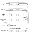
- FIG. 1 is a block diagram illustrating a configuration example of the electronic device 100 according to the embodiment of the present technology.
- the electronic device 100 is a device that converts an analog signal into a digital signal and processes it, and includes an analog signal supply unit 110, a reference clock supply unit 120, an analog-digital converter 200, and a digital signal processing unit 130.
- an imaging device, a wireless communication device, a measurement device, an information processing device, or the like is assumed.
- analog-digital converter 200 is provided in a device such as the electronic device 100, it may be provided in a module or device such as an image sensor or a measurement device.
- Analog signal supply unit 110 and supplies via the signal line 119 to the analog-to-digital converter 200 generates a voltage signal of the analog as an analog signal V in.
- a voltage signal of the analog For example, voice signals, image signals, is generated as an analog signal V in.
- the analog signal supply unit may generate an analog current signal.
- the analog signal supply unit 110 may receive an analog signal from the outside and supply the analog signal to the analog-digital converter 200.
- the reference clock supply unit 120 generates a reference clock signal REFCLK having a predetermined frequency as a clock signal to be referenced, and supplies the reference clock signal REFCLK to the analog-digital converter 200 via the signal line 129.
- Analog-to-digital converter 200 is synchronized with the reference clock signal REFCLK, and converts the analog signal V in to a digital signal D out.
- the analog-digital converter 200 supplies the converted digital signal Dout to the digital signal processing unit 130 via the signal line 209.
- the digital signal processing unit 130 performs predetermined processing such as image processing and sound processing on the digital signal Dout .
- the digital signal processing unit 130 is an example of a processing unit described in the claims.
- FIG. 2 is a block diagram illustrating a configuration example of the analog-digital converter 200 according to the embodiment.
- the analog-digital converter 200 includes a voltage-controlled oscillator 210, a comparison unit 220, a sampling clock generation unit 230, and a digital signal generation unit 240.
- Voltage controlled oscillator 210 is for generating a plurality of voltage controlled oscillation signal of a frequency corresponding to the signal level of the analog signal V in. For example, ten clock signals of VCO1 to VCO5 and XVCO1 to XVCO5 are generated as voltage controlled oscillation signals. These voltage controlled oscillation signals are signals having the same frequency and different phases.
- the voltage controlled oscillator 210 supplies these voltage controlled oscillation signals to the comparison unit 220.
- the voltage controlled oscillator 210 is an example of an oscillator described in the claims.
- the voltage-controlled oscillation signal is an example of an oscillation signal described in the claims.
- a current controlled oscillator that generates an oscillation signal having a frequency corresponding to the current level may be provided instead of the voltage controlled oscillator.
- the current signal is input to the analog-digital converter 200 as an analog signal.
- the sampling clock generator 230 generates a clock signal having a frequency higher than that of the reference clock signal REFCLK as the sampling clock signal SCLK.
- the sampling clock signal SCLK is generated by multiplying the reference clock signal REFCLK.
- the comparison unit 220 compares two voltage controlled oscillation signals (for example, VCO1 and XVCO1) having different phases with each other in synchronization with the sampling clock signal SCLK, and presents a plurality of (for example, 10) bits from the comparison result. Data Cur is generated. Each of the bits in the current data Cur indicates the value of the voltage controlled oscillation signal at each timing when the period of the voltage controlled oscillation signal is equally divided (for example, divided into 10). These bits are hereinafter referred to as “current bits”.
- the comparison unit 220 supplies the current data Cur to the digital signal generation unit 240.
- the comparison unit 220 is an example of a current bit generation unit described in the claims.
- Digital signal generation unit 240 in synchronization with the sampling clock signal SCLK, and generates a digital signal D out from the current data Cur. Details of the method of generating the digital signal Dout will be described later.
- FIG. 3 is a circuit diagram showing a configuration example of the voltage controlled oscillator 210 in the embodiment.
- the voltage-controlled oscillator 210 includes a voltage-current conversion circuit 211, an odd number of inverters 212, an odd number of inverters 213, an odd number of inverters 214, and an odd number of inverters 215. For example, five inverters are provided.
- Voltage-current converting circuit 211 is for converting the voltage of the analog signal V in to the current.
- the voltage-current conversion circuit 211 supplies the converted current signal I in to each of the inverters 212, 213, 214, and 215.
- the five inverters 212 and the five inverters 215 are each connected in a ring shape.
- Inverters 213 and 214 are connected to different inverters 212 and different inverters 215.
- the input terminal of the inverter 213 is connected to the output terminal of the inverter 212
- the output terminal of the inverter 213 is connected to the output terminal of the inverter 215.
- the input terminal of the inverter 214 is connected to the output terminal of the inverter 215, and the output terminal of the inverter 214 is connected to the output terminal of the inverter 212.
- the inverter ring composed of the inverter 212 and the inverter ring composed of the inverter 215 are connected by the latch composed of the inverters 213 and 214.
- the differential symmetry of the output waveform of each inverter ring becomes high, and it becomes easy to maintain the duty ratio of the waveform of the output signal at 50%.
- Inverter 212 in this configuration generates a voltage controlled oscillation signal of a frequency corresponding to the level of the current signal I in.
- the inverter 215 generates a clock signal having the same frequency as the voltage-controlled oscillation signal generated by the inverter 212 and having a phase different by half a cycle (in other words, inverted).
- the five inverters 212 supply the voltage control oscillation signals VCO1 to VCO5 to the comparison unit 220, and the five inverters 215 supply the voltage control oscillation signals XVCO1 to XVCO5 to the comparison unit 220.
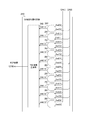
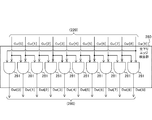
- FIG. 4 is a circuit diagram illustrating a configuration example of the comparison unit 220 in the embodiment.
- the comparison unit 220 includes an odd number of comparators 221, an odd number of latch circuits 222, and an odd number of flip-flops 223. For example, five comparators 221, latch circuits 222, and flip-flops 223 are provided.
- the comparator 221 compares two voltage controlled oscillation signals having different phases.
- the comparator 221 includes a clock terminal, input terminals D and Dn, and output terminals Q and Qn.
- the sampling clock signal SCLK is input to the clock terminal.
- the voltage-controlled oscillation signal VCOi is input to the input terminal D of the i-th (i is an integer from 1 to 5) comparator 221, and the voltage-controlled oscillation signal XVCOi is input to the input terminal Dn.
- the comparator 221 compares the levels of the voltage controlled oscillation signal VCOi and the voltage controlled oscillation signal XVCOi in synchronization with the sampling clock signal SCLK, and outputs the comparison result from the output terminal Q as a set signal. For example, a high level set signal is output when the voltage controlled oscillation signal VCOi is higher than the voltage controlled oscillation signal XVCOi, and a low level set signal is output otherwise. A signal obtained by inverting the set signal is output from the output terminal Qn as a reset signal.
- the latch circuit 222 outputs a comparison result based on the set signal and reset signal from the comparator 221.
- the latch circuit 222 is connected to different comparators 221 and includes a set terminal D, a reset terminal Dn, and an output terminal Q.
- a set signal from the corresponding comparator 221 is input to the set terminal D, and a reset signal is input to the reset terminal Dn.
- the latch circuit 222 outputs a high level signal from the output terminal Q when the set signal is high level and the reset signal is low level. When the set signal is low level and the reset signal is high level, the latch circuit 222 is low level.
- a signal is output from the output terminal Q.
- the flip-flop 223 holds the current bit.
- the flip-flop 223 is connected to different latch circuits 222 and includes a clock terminal, an input terminal D, and output terminals Q and Qn.
- the sampling clock signal SCLK is input to the clock terminal, and the input terminal D of the flip-flop 223 is connected to the output terminal Q of the corresponding latch circuit 222.
- the i-th flip-flop 223 holds the signal from the corresponding latch circuit 222 as the current bit Cur [i ⁇ 1], and outputs it from the output terminal Q in synchronization with the sampling clock signal SCLK.
- the flip-flop 223 outputs a signal obtained by inverting the current bit Cur [i ⁇ 1] as the current bit Cur [i + 4] from the output terminal Qn.
- the current data Cur including the current bits Cur [0] to Cur [9] is output from the five flip-flops 223 to the digital signal generation unit 240.
- FIG. 5 is a table showing an example of the operation of the comparator 221 in the embodiment.
- the comparator 221 outputs a set signal of “1” from the output terminal Q when the voltage controlled oscillation signal VCOi is higher than the voltage controlled oscillation signal XVCOi, and outputs a set signal of “0” from the output terminal Q otherwise. To do.
- the comparator 221 outputs a reset signal obtained by inverting the set signal from the output terminal Qn.
- FIG. 6 is a table showing an example of the operation of the latch circuit 222 in the embodiment.
- the latch circuit 222 outputs a signal of “0” from the output terminal Q when the set signal input to the input terminal D is “0” and the reset signal input to the input terminal Dn is “1”. To do.
- the latch circuit 222 outputs a signal “1” from the output terminal Q when the set signal is “1” and the reset signal is “0”. Further, when both the set signal and the reset signal are “0”, the latch circuit 222 shifts to a hold state in which the value of the output terminal Q is held.
- FIG. 7 is a truth table showing an example of the operation of the flip-flop 223 in the embodiment.
- the flip-flop 223 outputs the signal from the input terminal D from the output terminal Q as the current bit Cur [i-1] at the rising edge of the sampling clock signal SCLK.
- the flip-flop 223 holds the state of the output terminal Q in a period other than the rising edge of the sampling clock signal SCLK.
- the flip-flop 223 outputs a signal obtained by inverting the current bit Cur [i ⁇ 1] from the output terminal Qn.
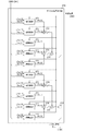
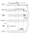
- FIG. 8 is a block diagram illustrating a configuration example of the digital signal generation unit 240 in the embodiment.
- the digital signal generation unit 240 includes a delay unit 241, a rising edge detection unit 250, a phase change amount determination unit 260, and a digital signal output unit 270.
- the delay unit 241 delays the current data Cur over the period of the sampling clock signal SCLK.
- the delay unit 241 supplies the delayed current data Cur to the phase change amount determination unit 260 and the digital signal output unit 270 as the delay data Del.
- Each bit in the delay data Del is hereinafter referred to as a “delay bit”.
- the rising edge detector 250 detects the presence or absence of a rising edge of the voltage controlled oscillation signal VCO at each of a plurality of (for example, 10) timings within the cycle of the voltage controlled oscillation signal VCO based on the current data Cur. It is.
- the rising edge detection unit 250 supplies the detection result Det to the phase change amount determination unit 260.
- This detection result Det includes a plurality of detection bits [j].
- j is an integer of 0 to 9, for example.
- a value of “1” is set for the detection bit at the timing when the rising edge is detected, and a value of “0” is set for the detection bit that is not.
- the rising edge detection unit 250 is an example of an edge detection unit described in the claims.
- the phase change amount determination unit 260 has a phase change amount (hereinafter referred to as “phase change amount”) of the voltage-controlled oscillation signal VCO in the cycle of the sampling clock signal SCLK as a half cycle (180 in angle notation). It is determined whether or not it is greater than (degree).
- the phase change amount determination unit 260 determines whether or not the phase change amount is large with respect to the half cycle depending on whether or not the values of the current bit and the delay bit corresponding to the timing detected when there is a rising edge are the same. Determine. For example, when the values of the current bit and the delay bit are the same, the phase change amount is less than a half cycle, and when they are different, it is determined that the phase change amount is greater than the half cycle.
- the phase change amount determination unit 260 supplies the determination result to the digital signal output unit 270.
- the phase change amount determination unit 260 is an example of a determination unit described in the claims.
- the digital signal output unit 270 generates and outputs a digital signal Dout based on the current data Cur, the delay data Del, and the determination result.
- the digital signal output unit 270 generates a digital signal Dout indicating a period in which the values of the delay bit and the current bit are in a specific combination when the phase change amount is equal to or less than a half cycle. For example, the digital signal Dout indicating the period in which the delay bit is “0” and the current bit is “1” is generated.
- the digital signal output unit 270 when the phase change amount is larger than a half cycle, the digital signal output unit 270 generates the digital signal Dout indicating the period in which the values of the delay bit and the current bit are the same or the specific combination described above. .
- a digital signal D out is generated that indicates a period in which both the delay bit and the current bit are “0” or “1”, or the delay bit is “0” and the current bit is “1”.
- the digital signal output unit 270 outputs the generated digital signal D out to the digital signal processing unit 130.
- the digital signal output unit 270 is an example of an output unit described in the claims.
- FIG. 9 is a circuit diagram illustrating a configuration example of the rising edge detection unit 250 according to the embodiment.
- the rising edge detection unit 250 includes a plurality of (for example, 10) AND (logical product) gates 251.
- the AND gate 251 outputs a logical product of two logical values.
- the 0th AND gate 251 outputs a logical product of the value obtained by inverting the current bit Cur [9] and the value of the current bit Cur [0] as the detection bit Det [0].
- the first and subsequent j-th AND gates 251 output a logical product of a value obtained by inverting the current bit Cur [j ⁇ 1] and the value of the current bit Cur [j] as a detection bit Det [j].
- FIG. 10 is a circuit diagram showing a configuration example of the phase change amount determination unit 260 in the embodiment.
- the phase change amount determination unit 260 includes a plurality of (for example, ten) AND gates 261 and a determination result generation unit 262.
- the AND gate 261 outputs a logical product of two logical values.
- the j-th AND gate 261 supplies the logical product of the delay bit Del [j] and the detection bit Det [j] to the determination result generation unit 262 as AND [j].
- the determination result generation unit 262 generates a determination result based on AND [0] to AND [9].
- the fact that AND [0] to AND [9] are all “0” indicates that the values of the current bit and the delay bit corresponding to the detected timing are different when there is a rising edge.
- the determination result generation unit 262 determines that the phase change amount is greater than a half cycle, and generates a determination result of a value of “0”, for example.
- the determination result generation unit 262 determines that the phase change amount is equal to or less than a half cycle, and generates a determination result having a value of “1”, for example.
- FIG. 11 is a table showing an example of the operation of the determination result generation unit 262 in the embodiment.
- the determination result generation unit 262 determines that the phase change amount is larger than a half cycle, and generates a determination result of a value of “0”, for example.
- the determination result generation unit 262 determines that the phase change amount is equal to or less than a half cycle, for example, a value of “1”. A determination result is generated.
- the determination result generation unit 262 generates a determination result of a value “1” when it is determined that the phase change amount is greater than a half cycle, and generates a determination result of a value “0” otherwise. May be.
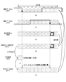
- FIG. 12 is a circuit diagram illustrating a configuration example of the digital signal output unit 270 in the embodiment.
- the digital signal output unit 270 includes a plurality of (for example, 10) arithmetic circuits 271 and adders 272 to 278.
- the arithmetic circuit 271 determines whether the values of the current bit Cur [j] and the delay bit Del [j] are the same or a specific combination when the phase change amount is larger than a half cycle, and the determination result Is generated as the operation result Ph [j].
- the specific combination is, for example, a combination in which the delay bit Del [j] is “0” and the current bit Cur [j] is “1”. Further, for example, when the values of the current bit Cur [j] and the delay bit Del [j] are the same or a specific combination, a value of “1” is set in the operation result Ph [j]. If not, a value of “0” is set.
- the arithmetic circuit 271 determines whether or not the values of the current bit [j] and the delay bit Del [j] are a specific combination, and indicates the determination result. Is generated as the calculation result Ph [h].
- a value of “1” is set when the values of the current bit Cur [j] and the delay bit Del [j] are a specific combination, and “0” otherwise. The value of is set.
- the adder 272 adds the values of the operation results Ph [0] and Ph [1] and supplies the addition result to the adder 274.
- the adder 273 adds the values of the operation results Ph [2], Ph [3], and Ph [4] and supplies the addition result to the adder 274.
- the adder 274 adds the addition results of the adders 272 and 273 and supplies the result to the adder 278.
- the adder 275 adds the values of the operation results Ph [5] and Ph [6] and supplies the result to the adder 277.
- the adder 276 adds the respective values of the calculation results Ph [7], Ph [8], and Ph [9] and supplies the addition result to the adder 277.
- the adder 277 adds the addition results of the adders 275 and 276 and supplies the result to the adder 278.
- the adder 278 adds the addition results of the adders 274 and 277 and outputs a signal indicating the addition result as a digital signal Dout .
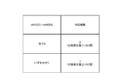
- FIG. 13 is a table showing an example of the operation of the arithmetic circuit 271 in the embodiment.
- the arithmetic circuit 271 has the same condition that the delay bit Del [j] is “0” and the current bit [j] is “1”, and the values of the delay bit Del [j] and the current bit [j] are the same. If any of the conditions is satisfied, an operation result Ph [j] of “1” is generated. On the other hand, the arithmetic circuit 271 generates a calculation result Ph [j] of “0” if those conditions are not satisfied.
- the operation result Ph [j] is generated by a different logical operation.
- the arithmetic circuit 271 generates an operation result Ph [j] of “1” if the delay bit Del [j] is “0” and the current bit [j] is “1”, otherwise “ An operation result Ph [j] of “0” is generated.
- FIG. 14 is a diagram illustrating an example of edge positions indicated by the delay data and the current data when the phase change amount is 180 degrees or less in the embodiment.
- the angle of each of the ten straight lines extending radially from the center of the circle with respect to a specific straight line indicates the respective phases of the timing obtained by dividing the period of the voltage controlled oscillation signal into ten. Since 360 degrees is divided into 10 parts, the angles are 36 degrees different from each other.
- the hatched section indicates a period in which the value of the voltage controlled oscillation signal is “1”.
- the fourth timing is the falling edge timing.
- b in the figure is a diagram showing an example of the timing of the falling edge of the voltage controlled oscillation signal VCO indicated by the current data.
- FIG. 15 is a diagram for explaining a calculation method when the phase change amount is 180 degrees or less in the embodiment.
- “a” is a diagram illustrating an example of the delay data Del generated by the delay unit 241.
- the thick solid line indicates the waveform of the voltage controlled oscillation signal VCO.
- the delay data Del includes 10 delay bits, and each bit indicates the value of the voltage controlled oscillation signal VCO at each timing obtained by dividing the period of the voltage controlled oscillation signal VCO by 10.
- 15b is a diagram illustrating an example of the current data Cur generated by the comparison unit 220.
- the thick solid line shows the waveform of the voltage controlled oscillation signal VCO.
- the current data Cur includes 10 current bits, and each bit indicates the value of the voltage controlled oscillation signal VCO at each timing obtained by dividing the period of the voltage controlled oscillation signal VCO by 10.
- the detection result Det includes 10 detection bits, and each bit indicates the presence / absence of a rising edge at each of timings obtained by dividing the period of the voltage controlled oscillation signal VCO by 10. Here, it is detected that there is a rising edge in the fourth detection bit.
- 15 is a diagram illustrating an example of AND [0] to AND [9] generated by the AND gate 261.
- a logical product of the delay bit and the detection result bit is generated as AND [0] to AND [9]. Since the fourth bit is detected as having a rising edge, and the fourth delay bit is also “1”, AND [4] which is a logical product of them is a value of “1”. AND [4] being “1” indicates that the current bit and the delay bit corresponding to the fourth timing detected as having a rising edge have the same value.
- 15 is a diagram illustrating an example of the determination result generated by the determination result generation unit 262. Since AND [5] is “1”, a determination result “1” indicating that the amount of phase change is 180 degrees or less is generated.
- the arithmetic circuit 271 When the phase change amount is 180 degrees or less, the arithmetic circuit 271 generates the arithmetic result “j” having the value “1” at the timing when the delay bit becomes “0” and the current bit becomes “1”. .
- the delay bit is “0” and the current bit is “1” at the sixth to eighth timings, the operation results Ph “6” to Ph “8” of the value “1” are generated.
- a period “3” consisting of these timings is calculated as the phase change amount.
- FIG. 16 is a diagram illustrating an example of edge positions indicated by the delay data and the current data when the phase change amount is greater than 180 degrees in the embodiment.
- a is a diagram showing an example of the timing of the falling edge of the voltage controlled oscillation signal VCO indicated by the delay data.
- the 0th timing is the timing of the falling edge.
- b in the figure is a diagram showing an example of the timing of the falling edge of the voltage controlled oscillation signal VCO indicated by the current data.
- FIG. 17 is a diagram for explaining a calculation method when the phase change amount in the embodiment is larger than 180 degrees.
- “a” is a diagram illustrating an example of the delay data Del generated by the delay unit 241.
- B in the figure shows an example of the current data Cur generated by the comparison unit 220.
- 17 is a diagram illustrating an example of the detection result Det of the rising edge detected from the current data by the rising edge detection unit 250. Here, it is detected that there is a rising edge in the third detection bit.
- 17 is a diagram illustrating an example of AND [0] to AND [9] generated by the AND gate 261. Since it is the third bit detected that there is a rising edge and the third delay bit is “0”, AND [3] which is the logical product of them is a value of “0”. AND [3] being “0” indicates that the current bit and the delay bit corresponding to the third timing detected as having a rising edge are different values.
- E in FIG. 17 is a diagram illustrating an example of a determination result generated by the determination result generation unit 262. Since all of AND [j] are “0”, a determination result of “0” indicating that the amount of phase change is greater than 180 degrees is generated.
- 17 is a diagram illustrating an example of a calculation result Ph [j] by the calculation circuit 271.
- the arithmetic circuit 271 sets “1” at the timing when the delay bit is “0” and the current bit is “1” and when the value of the delay bit and the current bit is the same.
- the operation result Ph “j” of the value of is generated.
- the calculation results Ph “1” to Ph “7” of the value “1” are generated at the first to seventh timings. A period “7” consisting of these timings is calculated as the phase change amount.
- phase change amount is calculated. This amount of phase change is not an accurate value (“7”). As a result, there is a possibility that the S / N ratio of the analog-digital converter is lowered.
- the analog-to-digital converter 200 switches the calculation method depending on whether or not the phase change amount in the sampling period is larger than 180 in the clock signal having a period corresponding to the signal level of the analog signal. ing. Therefore, the analog-digital converter 200 can calculate an accurate phase change amount even when the phase change amount is greater than 180 degrees.
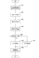
- FIG. 18 is a flowchart illustrating an example of the operation of the analog-digital converter 200 according to the embodiment. This operation is repeatedly executed in synchronization with the sampling clock signal SCLK, for example.
- the analog-digital converter 200 generates a voltage controlled oscillation signal VCO having a frequency corresponding to the signal level of the analog signal (step S901).
- the analog-digital converter 200 acquires current data (step S902) and acquires delay data (step S903).
- the analog-digital converter 200 detects the rising edge timing in the current data (step S904).
- the analog-to-digital converter 200 determines whether or not the phase change amount is 180 degrees or less depending on whether or not the current bit and the past bit corresponding to the detected edge timing are the same value (step). S905).
- step S905: Yes the analog-digital converter 200 counts the number of bits changed from “0” to “1” (step S906).
- step S905: No the analog-to-digital converter 200 counts the number of bits between the bit that has changed from “0” to “1” and the bit that does not change the value.
- Step D907 the analog-to-digital converter 200 generates and outputs a digital signal indicating the count value (step S908).
- step S908 the analog-to-digital converter 200 ends the sampling operation.
- the analog-to-digital converter determines whether or not the phase change amount is larger than a half cycle in the clock signal having a cycle according to the signal level of the analog signal.
- the phase change amount can be accurately obtained from the determination result.
- an analog signal can be accurately converted into a digital signal.
- the analog-digital converter 200 detects the rising edge, but may detect the falling edge instead of the rising edge.
- the analog-digital converter 200 of the first modification is different from the embodiment in that it detects a falling edge instead of a rising edge.
- the digital signal generation unit 240 includes a falling edge detection unit 280 instead of the rising edge detection unit 250.
- FIG. 19 is a circuit diagram showing a configuration example of the falling edge detection unit 280 in the first modification of the embodiment.
- the falling edge detection unit 280 includes a plurality of (for example, 10) AND (logical product) gates 281.
- the AND gate 281 outputs a logical product of two logical values.
- the 0th AND gate 281 outputs a logical product of the current bit Cur [9] value and the inverted value of the current bit Cur [0] as the detection bit Det [0].
- the first and subsequent j-th AND gates 281 output the logical product of the value of the current bit Cur [j ⁇ 1] and the inverted value of the current bit Cur [j] as the detection bit Det [j].
- the determination result generation unit 262 of the first modification determines that the amount of phase change is equal to or less than a half cycle when AND [0] to AND [9] are all “0”, and the value of “0” The determination result is generated. On the other hand, when any of AND [0] to AND [9] is “1”, the determination result generation unit 262 determines that the phase change amount is greater than a half cycle, and determines the determination result of the value “1”. Generate.
- FIG. 20 is a diagram for explaining a calculation method when the phase change amount is 180 degrees or less in the first modification example of the embodiment.
- “a” is a diagram illustrating an example of the delay data Del generated by the delay unit 241.
- B in the figure shows an example of the current data Cur generated by the comparison unit 220.
- 20 is a diagram illustrating an example of the detection result Det of the falling edge detected from the current data by the falling edge detection unit 280. Here, it is detected that there is a falling edge in the ninth detection bit.
- FIG. 20 is a diagram illustrating an example of AND [0] to AND [9] generated by the AND gate 261. Since the 9th bit is detected as having a falling edge and the 9th delay bit is “0”, AND [9] which is a logical product of them is a value of “0”. AND [9] being “0” indicates that the current bit and the delay bit corresponding to the ninth timing detected as having a falling edge have the same value.
- 20 is a diagram illustrating an example of a determination result generated by the determination result generation unit 262. Since all of AND [j] are “0”, a determination result of “0” indicating that the amount of phase change is 180 degrees or less is generated.
- FIG. 21 is a diagram for explaining a calculation method when the phase change amount exceeds 180 degrees in the first modification of the embodiment.
- “a” is a diagram illustrating an example of the delay data Del generated by the delay unit 241.
- B in the figure shows an example of the current data Cur generated by the comparison unit 220.
- 21c is a diagram illustrating an example of a falling edge detection result Det detected from the current data by the falling edge detection unit 280.
- FIG. Here, it is detected that there is a falling edge in the eighth detection bit.
- 21 is a diagram illustrating an example of AND [0] to AND [9] generated by the AND gate 261. Since it is the 8th bit detected that there is a falling edge and the 8th delay bit is “1”, AND [8] which is the logical product of them is a value of “1”. That AND [8] is “1” indicates that the current bit and the delay bit corresponding to the eighth timing detected as having a falling edge are different values.
- 21 is a diagram illustrating an example of the determination result generated by the determination result generation unit 262. Since AND [8] is “1”, a determination result “1” indicating that the amount of phase change is greater than 180 degrees is generated.
- 21 is a diagram illustrating an example of a calculation result Ph [j] by the calculation circuit 271. Similar to the embodiment, calculation results Ph [1] to Ph [7] having a value of “1” are generated at the first to seventh timings.
- the analog-digital converter 200 detects the falling edge from the current data, and therefore the phase change amount is larger than a half cycle from the detection result of the falling edge and the delay data. It can be determined whether or not.
- the analog-digital converter 200 detects the rising edge from the current data Cur, but may detect the rising edge from the delay data Del.
- the analog-to-digital converter 200 of the first modified example is different from the embodiment in that the rising edge is detected from the delay data Del.
- FIG. 22 is a block diagram illustrating a configuration example of the digital signal generation unit 240 in the second modification of the embodiment.
- Delay data Del is input to the rising edge detector 250 of the second modified example instead of the current data Cur.
- the detection result Det and the current data Cur are input to the phase change amount determination unit 260 of the second modification.
- the configuration of the determination result generation unit 262 in the phase change amount determination unit 260 of the second modification is the same as that of the first modification.
- FIG. 23 is a diagram for explaining a calculation method when the amount of phase change in the second modification of the embodiment is 180 degrees or less.
- “a” is a diagram illustrating an example of the delay data Del generated by the delay unit 241.
- B in the figure shows an example of the current data Cur generated by the comparison unit 220.
- FIG. 23 is a diagram illustrating an example of the rising edge detection result Det detected from the delay data by the rising edge detection unit 250. Here, it is detected that there is a rising edge in the first detection bit.
- FIG. 23 is a diagram illustrating an example of AND [0] to AND [9] generated by the AND gate 261. Since it is the first bit detected that there is a rising edge and the first current bit is “0”, AND [1] which is the logical product of them is a value of “0”. AND [1] being “0” indicates that the current bit and the delay bit corresponding to the first timing detected as having a rising edge are different values.
- FIG. 23 is a diagram illustrating an example of the determination result generated by the determination result generation unit 262. Since all of AND [j] are “0”, a determination result of “0” indicating that the amount of phase change is 180 degrees or less is generated.
- FIG. 24 is a diagram for explaining a calculation method when the phase change amount exceeds 180 degrees in the second modification of the embodiment.
- “a” is a diagram illustrating an example of the delay data Del generated by the delay unit 241.
- B in the figure shows an example of the current data Cur generated by the comparison unit 220.
- C in FIG. 24 is a diagram illustrating an example of the detection result Det of the rising edge detected from the delay data by the rising edge detection unit 250. Here, it is detected that there is a rising edge in the sixth detection bit.
- FIG. 24 is a diagram illustrating an example of AND [0] to AND [9] generated by the AND gate 261. Since it is the sixth bit detected that there is a rising edge and the sixth current bit is “1”, AND [6], which is the logical product of them, has a value of “1”. That AND [6] is “1” indicates that the current bit and the delay bit corresponding to the sixth timing detected as having a rising edge have the same value.
- FIG. 24 is a diagram illustrating an example of the determination result generated by the determination result generation unit 262. Since AND [6] is “1”, a determination result “1” indicating that the amount of phase change is greater than 180 degrees is generated.
- 24f is a diagram illustrating an example of a calculation result Ph [j] by the calculation circuit 271. Similar to the embodiment, calculation results Ph [1] to Ph [1] having a value of “1” are generated at the first to seventh timings.
- the analog-digital converter 200 detects the rising edge from the delay data, and therefore determines whether or not the phase change amount is larger than a half cycle from the detection result and the current data. can do.
- the analog-digital converter 200 detects the rising edge from the current data Cur, but may detect the falling edge from the delay data Del.
- the analog-to-digital converter 200 of the third modified example is different from that of the embodiment in that the falling edge is detected from the delay data Del.
- the digital signal generation unit 240 of the third modification example is the same as that of the second modification example illustrated in FIG. 22 in that a falling edge detection unit 280 of the first modification example is provided instead of the rising edge detection unit 250. Different from the configuration.
- FIG. 25 is a diagram for explaining a calculation method when the amount of phase change is 180 degrees or less in the third modification of the embodiment.
- “a” is a diagram illustrating an example of the delay data Del generated by the delay unit 241.
- B in the figure shows an example of the current data Cur generated by the comparison unit 220.
- C in FIG. 25 is a diagram illustrating an example of a falling edge detection result Det detected from the delay data by the falling edge detection unit 280. Here, it is detected that there is a falling edge in the sixth detection bit.
- 25 is a diagram illustrating an example of AND [0] to AND [9] generated by the AND gate 261. Since the sixth bit is detected as having a falling edge and the sixth current bit is “1”, AND [6] which is the logical product of them is a value of “1”. That AND [6] is “1” indicates that the current bit and the delay bit corresponding to the sixth timing detected as having a falling edge are different values.
- E in FIG. 25 is a diagram illustrating an example of a determination result generated by the determination result generation unit 262. Since AND [6] is “1”, a determination result “1” indicating that the amount of phase change is 180 degrees or less is generated.
- 25f is a diagram illustrating an example of the calculation result Ph [j] by the calculation circuit 271.
- calculation results Ph [6] to Ph [8] having a value of “1” are generated at the sixth to eighth timings.
- FIG. 26 is a diagram for explaining a calculation method when the phase change amount exceeds 180 degrees in the third modification of the embodiment.
- “a” is a diagram illustrating an example of the delay data Del generated by the delay unit 241.
- B in the figure shows an example of the current data Cur generated by the comparison unit 220.
- 26c is a diagram showing an example of the falling edge detection result Det detected from the delay data by the falling edge detector 280.
- FIG. Here, it is detected that there is a falling edge in the first detection bit.
- 26 is a diagram illustrating an example of AND [0] to AND [9] generated by the AND gate 261. Since it is the first bit detected that there is a falling edge and the first current bit is “0”, AND [1] which is the logical product of them is a value of “0”. AND [1] being “0” indicates that the current bit and the delay bit corresponding to the first timing detected as having a falling edge have the same value.
- 26 is a diagram illustrating an example of a determination result generated by the determination result generation unit 262. Since all of AND [j] are “0”, a determination result of “0” indicating that the amount of phase change is greater than 180 degrees is generated.
- 26f is a diagram illustrating an example of a calculation result Ph [j] by the calculation circuit 271. Similar to the embodiment, calculation results Ph [1] to Ph [1] having a value of “1” are generated at the first to seventh timings.
- the analog-to-digital converter 200 detects the falling edge from the delay data, so whether or not the phase change amount is larger than a half cycle from the detection result and the current data. Can be determined.
- the processing procedure described in the above embodiment may be regarded as a method having a series of these procedures, and a program for causing a computer to execute these series of procedures or a recording medium storing the program. You may catch it.
- a recording medium for example, a CD (Compact Disc), an MD (MiniDisc), a DVD (Digital Versatile Disc), a memory card, a Blu-ray disc (Blu-ray (registered trademark) Disc), or the like can be used.
- this technique can also take the following structures.
- an oscillator that generates an oscillation signal having a period according to the signal level of the input analog signal;
- a current bit generating unit that generates a bit indicating a value of the oscillation signal as a current bit at each of a plurality of timings in the cycle;
- a delay unit that delays each of the current bits over a predetermined period and supplies the delayed bits as a delay bit;
- a determination unit that determines whether or not the amount of change in the phase of the oscillation signal within the predetermined period is greater than a half period of the period; If the change amount is not greater than the half cycle, data indicating a period in which the values of the current bit and the delay bit are in a specific combination is generated and output, and the change amount is greater than the half cycle.
- the analog-digital converter includes an output unit that generates and outputs data indicating a period in which the values of the current bit and the delay bit are the same or the specific combination.
- (2) further comprising an edge detector that detects the presence or absence of one of rising and falling edges of the oscillation signal based on either the current bit or the delay bit, corresponding to each of the plurality of timings; The determination unit determines that the amount of change is larger than the half cycle depending on whether the current bit and the delay bit corresponding to the timing detected as having the one edge are the same.
- the analog-digital converter according to the above (1) which detects whether or not.
- (3) The analog-digital converter according to (2), wherein the edge detection unit detects the presence or absence of the one edge based on the delay bit.
- the edge detection unit detects the presence or absence of the rising edge based on the delay bit, The determination unit determines that the amount of change is not greater than the half cycle when the current bit corresponding to the timing detected as having the rising edge is at a low level, and the current bit is high.
- the edge detection unit detects the presence or absence of the falling edge based on the delay bit, The determination unit determines that the amount of change is not greater than the half cycle when the current bit corresponding to the timing detected as having the falling edge is at a high level, and the current bit is The analog-digital converter according to (3), wherein when it is at a low level, the change amount is determined to be greater than the half cycle. (6) The analog-digital converter according to (2), wherein the edge detection unit detects the presence or absence of the one edge based on the current bit.
- the edge detection unit detects the presence or absence of the rising edge based on the current bit, The determination unit determines that the amount of change is not greater than the half cycle when the delay bit corresponding to the timing detected as having the rising edge is at a high level, and the delay bit is low.
- the edge detection unit detects the presence or absence of the falling edge based on the current bit, The determination unit determines that the amount of change is not greater than the half cycle when the delay bit corresponding to the timing detected as having the falling edge is at a low level, and the delay bit is The analog-to-digital converter according to (6), wherein when the level is high, the change amount is determined to be larger than the half cycle. (9) When the change amount is not larger than the half cycle, the output unit counts the number of the timings that are the current specific combination and generates data of the count value as data indicating the period.
- the analog-digital converter according to any one of (1) to (8), which is generated as data to be indicated.
- an oscillator that generates an oscillation signal having a period according to the signal level of the input analog signal;
- a current bit generating unit that generates a bit indicating a value of the oscillation signal as a current bit at each of a plurality of timings in the cycle;
- a delay unit that delays each of the current bits over a predetermined period and supplies the delayed bits as a delay bit;
- a determination unit that determines whether or not the amount of change in the phase of the oscillation signal within the predetermined period is greater than a half period of the period; If the change amount is not greater than the half cycle, data indicating a period in which the values of the current bit and the delay bit are in a specific combination is generated and output, and the change amount is greater than the half cycle.
- an output unit that generates and outputs data indicating a period in which each value of the current bit and the delay bit is the same or the specific combination;
- An electronic device comprising: a processing unit that processes the data. (11) an oscillation procedure in which an oscillator generates an oscillation signal having a period corresponding to the signal level of an input analog signal; A current bit generation unit that generates a bit indicating a value of the oscillation signal as a current bit at each of a plurality of timings in the cycle; A delay procedure in which a delay unit delays each of the current bits for a predetermined period and supplies the delayed bits as a delay bit; A determination procedure for determining whether the amount of change in which the phase of the oscillation signal has changed within the predetermined period is greater than a half period of the period; The output unit generates and outputs data indicating a period in which each value of the current bit and the delay bit is a specific combination when the amount of change is not greater than the half cycle, and the amount of change is A method for controlling an analog-
Abstract
Priority Applications (2)
| Application Number | Priority Date | Filing Date | Title |
|---|---|---|---|
| US15/500,547 US9793914B2 (en) | 2014-08-12 | 2015-06-16 | Analog-to-digital converter, electronic device, and method of controlling analog-to-digital converter |
| JP2016542514A JP6564378B2 (ja) | 2014-08-12 | 2015-06-16 | アナログデジタル変換器、電子装置、および、アナログデジタル変換器の制御方法 |
Applications Claiming Priority (2)
| Application Number | Priority Date | Filing Date | Title |
|---|---|---|---|
| JP2014164568 | 2014-08-12 | ||
| JP2014-164568 | 2014-08-12 |
Publications (1)
| Publication Number | Publication Date |
|---|---|
| WO2016024439A1 true WO2016024439A1 (fr) | 2016-02-18 |
Family
ID=55304069
Family Applications (1)
| Application Number | Title | Priority Date | Filing Date |
|---|---|---|---|
| PCT/JP2015/067297 WO2016024439A1 (fr) | 2014-08-12 | 2015-06-16 | Convertisseur analogique-numérique, dispositif électronique, et procédé de commande pour convertisseur analogique-numérique |
Country Status (3)
| Country | Link |
|---|---|
| US (1) | US9793914B2 (fr) |
| JP (1) | JP6564378B2 (fr) |
| WO (1) | WO2016024439A1 (fr) |
Cited By (1)
| Publication number | Priority date | Publication date | Assignee | Title |
|---|---|---|---|---|
| JPWO2017163528A1 (ja) * | 2016-03-22 | 2019-01-24 | ソニー株式会社 | 電子回路、および、電子回路の制御方法 |
Families Citing this family (2)
| Publication number | Priority date | Publication date | Assignee | Title |
|---|---|---|---|---|
| US10212500B2 (en) * | 2017-01-27 | 2019-02-19 | Apple Inc. | Digital transducer circuit |
| TR202002360A2 (tr) * | 2020-02-17 | 2021-08-23 | Tobb Ekonomi Ve Teknoloji Ueniverisitesi | Hassasliği artirilmiş bi̇r karşilaştirma devresi̇ |
Citations (4)
| Publication number | Priority date | Publication date | Assignee | Title |
|---|---|---|---|---|
| US8063810B2 (en) * | 2009-07-30 | 2011-11-22 | Freescale Semiconductor, Inc. | Unfolding VCO-based quantization circuit |
| US20120112936A1 (en) * | 2010-11-04 | 2012-05-10 | Sheng-Jui Huang | Quantization circuit having vco-based quantizer compensated in phase domain and related quantization method and continuous-time delta-sigma analog-to-digital converter |
| US20120154192A1 (en) * | 2009-08-28 | 2012-06-21 | Op T Eynde Frank | Voltage controlled oscillator (vco) based analog-digital converter |
| US20120194369A1 (en) * | 2011-01-28 | 2012-08-02 | The Regents Of The University Of California | Ring oscillator delta sigma adc modulator with replica path nonlinearity calibration |
Family Cites Families (7)
| Publication number | Priority date | Publication date | Assignee | Title |
|---|---|---|---|---|
| US3714375A (en) * | 1970-10-16 | 1973-01-30 | Collins Radio Co | Secondary phase modulated communications service via am broadcast stations |
| JP3983449B2 (ja) * | 1999-10-15 | 2007-09-26 | 株式会社リコー | パルス幅変調回路、光書き込み装置及び画像形成装置 |
| JP2001332034A (ja) * | 2000-05-24 | 2001-11-30 | Sony Corp | Pll回路およびこれを用いた記録再生装置 |
| US7177610B2 (en) * | 2001-01-12 | 2007-02-13 | Silicon Laboratories Inc. | Calibrated low-noise current and voltage references and associated methods |
| US6956518B1 (en) * | 2004-03-31 | 2005-10-18 | Silicon Labs Cp, Inc. | Method and apparatus for subclocking a SAR analog-to-digital converter |
| US7528760B2 (en) * | 2007-01-26 | 2009-05-05 | Texas Insturments Incorporated | Class D analog-to-digital converter |
| US7915935B1 (en) * | 2009-11-13 | 2011-03-29 | Anokiwave, Inc. | Communication systems w/counter-based frequency centering for mm-wave frequency bands |
-
2015
- 2015-06-16 JP JP2016542514A patent/JP6564378B2/ja active Active
- 2015-06-16 WO PCT/JP2015/067297 patent/WO2016024439A1/fr active Application Filing
- 2015-06-16 US US15/500,547 patent/US9793914B2/en active Active
Patent Citations (4)
| Publication number | Priority date | Publication date | Assignee | Title |
|---|---|---|---|---|
| US8063810B2 (en) * | 2009-07-30 | 2011-11-22 | Freescale Semiconductor, Inc. | Unfolding VCO-based quantization circuit |
| US20120154192A1 (en) * | 2009-08-28 | 2012-06-21 | Op T Eynde Frank | Voltage controlled oscillator (vco) based analog-digital converter |
| US20120112936A1 (en) * | 2010-11-04 | 2012-05-10 | Sheng-Jui Huang | Quantization circuit having vco-based quantizer compensated in phase domain and related quantization method and continuous-time delta-sigma analog-to-digital converter |
| US20120194369A1 (en) * | 2011-01-28 | 2012-08-02 | The Regents Of The University Of California | Ring oscillator delta sigma adc modulator with replica path nonlinearity calibration |
Cited By (1)
| Publication number | Priority date | Publication date | Assignee | Title |
|---|---|---|---|---|
| JPWO2017163528A1 (ja) * | 2016-03-22 | 2019-01-24 | ソニー株式会社 | 電子回路、および、電子回路の制御方法 |
Also Published As
| Publication number | Publication date |
|---|---|
| US9793914B2 (en) | 2017-10-17 |
| JPWO2016024439A1 (ja) | 2017-05-25 |
| US20170222655A1 (en) | 2017-08-03 |
| JP6564378B2 (ja) | 2019-08-21 |
Similar Documents
| Publication | Publication Date | Title |
|---|---|---|
| US7688242B2 (en) | Analog-to-digital (AD) converter and analog-to-digital conversion method | |
| US9092013B2 (en) | Time-to-digital converter | |
| JP5590867B2 (ja) | タイム/デジタルコンバーター及びデジタル位相ロックループ | |
| EP2490336B1 (fr) | Suivi de convertisseur analogique à numérique au moyen d'une horloge variable auto-contrôlée | |
| US11042126B2 (en) | Time-to-digital converter | |
| KR20150129794A (ko) | 임베딩된 t2v adc를 가진 혼합된 신호 tdc | |
| JP2018125791A (ja) | Cdr回路及び受信回路 | |
| WO2013069173A1 (fr) | Convertisseur numérique de différence de temps | |
| US9716508B1 (en) | Dummy signal generation for reducing data dependent noise in digital-to-analog converters | |
| US10819355B1 (en) | Phase to digital converter | |
| US9405275B2 (en) | Time-to-digital converter and related method | |
| US10886930B1 (en) | Voltage controlled oscillator based analog-to-digital converter including a maximum length sequence generator | |
| US9250612B2 (en) | System and method for a time-to-digital converter | |
| JP6564378B2 (ja) | アナログデジタル変換器、電子装置、および、アナログデジタル変換器の制御方法 | |
| WO2019146177A1 (fr) | Circuit de conversion temps-numérique et boucle à phase asservie | |
| US10270460B1 (en) | Coarse-fine quantization architecture for multiphase VCO-based ADCs | |
| JP6433955B2 (ja) | 高分解能の時間−ディジタル変換器 | |
| CN109412598B (zh) | 一种逐次逼近式模数转换装置 | |
| JPWO2010016301A1 (ja) | 位相比較器、pll回路およびdll回路 | |
| TWI568195B (zh) | 時間至數位轉換器 | |
| JP3218720B2 (ja) | 入力信号のエッジ時刻測定回路及びディジタルpll装置 | |
| JP3257065B2 (ja) | ディジタルpll装置 | |
| JP4000472B2 (ja) | 位相比較器 | |
| JP2016187085A (ja) | 逐次比較型a/d変換方法および逐次比較型a/d変換器 | |
| JP2017123613A (ja) | A/D(Analog/Digital)変換回路並びにA/D変換方法 |
Legal Events
| Date | Code | Title | Description |
|---|---|---|---|
| 121 | Ep: the epo has been informed by wipo that ep was designated in this application |
Ref document number: 15831701 Country of ref document: EP Kind code of ref document: A1 |
|
| ENP | Entry into the national phase |
Ref document number: 2016542514 Country of ref document: JP Kind code of ref document: A |
|
| WWE | Wipo information: entry into national phase |
Ref document number: 15500547 Country of ref document: US |
|
| NENP | Non-entry into the national phase |
Ref country code: DE |
|
| 122 | Ep: pct application non-entry in european phase |
Ref document number: 15831701 Country of ref document: EP Kind code of ref document: A1 |