WO2016009924A1 - 演算増幅回路 - Google Patents
演算増幅回路 Download PDFInfo
- Publication number
- WO2016009924A1 WO2016009924A1 PCT/JP2015/069681 JP2015069681W WO2016009924A1 WO 2016009924 A1 WO2016009924 A1 WO 2016009924A1 JP 2015069681 W JP2015069681 W JP 2015069681W WO 2016009924 A1 WO2016009924 A1 WO 2016009924A1
- Authority
- WO
- WIPO (PCT)
- Prior art keywords
- current source
- current
- selector
- state
- output
- Prior art date
- Legal status (The legal status is an assumption and is not a legal conclusion. Google has not performed a legal analysis and makes no representation as to the accuracy of the status listed.)
- Ceased
Links
Images


Classifications
-
- H—ELECTRICITY
- H03—ELECTRONIC CIRCUITRY
- H03F—AMPLIFIERS
- H03F3/00—Amplifiers with only discharge tubes or only semiconductor devices as amplifying elements
- H03F3/34—DC amplifiers in which all stages are DC-coupled
-
- H—ELECTRICITY
- H03—ELECTRONIC CIRCUITRY
- H03F—AMPLIFIERS
- H03F3/00—Amplifiers with only discharge tubes or only semiconductor devices as amplifying elements
- H03F3/45—Differential amplifiers
Definitions
- the present invention relates to an operational amplifier circuit, and more particularly to a circuit technique for reducing the offset voltage and 1 / f noise of the operational amplifier circuit.
- Operational amplifier circuits are used in a wide range of applications in semiconductor integrated circuits.
- semiconductor integrated circuits manufactured by a CMOS process are mainly used at present, so that an operational amplifier circuit is also composed of MOS transistors.
- Non-Patent Documents 1 and 2 Non-Patent Documents 1 and 2 and (Patent Documents 1 to 5).
- FIG. 1 shows an operational amplifier circuit using a chopper modulation technique.
- the chopper circuits 1 and 3 are provided at the input and output of the operational amplifier circuit 2, respectively, and the modulation operation is performed at the modulation frequency FCHOP.
- the input signal is modulated by an input chopper circuit, and the modulated signal is amplified by an operational amplifier circuit and demodulated by an output chopper circuit. Since the signal is amplified at a modulated high frequency, the influence of the offset voltage of the operational amplifier circuit and 1 / f noise can be removed.
- the offset voltage and 1 / f noise of the operational amplifier circuit are modulated by the output chopper circuit to the modulation frequency FCHOP and its odd harmonics, the offset voltage and 1 / f noise appear at the low frequency of the output. Absent.
- An operational amplifier circuit using a chopper modulation technique is used for various applications by utilizing the characteristics of a low offset voltage and 1 / f noise.
- the modulated offset voltage of the operational amplifier circuit or the 1 / f noise component becomes a problem in terms of characteristics, it is necessary to provide a low-pass filter to remove it.
- the input and output voltages of the normal phase and the reverse phase to the operational amplifier circuit 2 are alternately switched by the chopper circuits 1 and 3, so that both the frequency characteristic and the slew rate of the operational amplifier circuit 2 are obtained. High performance is required.
- the terminals OUTP_I and OUTM_I of the operational amplifier circuit 2 need to change from the maximum value to the minimum value of the sine wave at time 0.5 / FCHOP. . That is, the frequency characteristics and the slew rate need to be higher than necessary for the signal to be amplified. In addition, the lack of frequency characteristics and slew rate causes distortion.
- Patent Document 5 divides an operational amplifier circuit using a chopper modulation technique into two or more segments as shown by 4a and 4b in FIG. 2, and determines the number of operational amplifier circuits whose states change at a time. By reducing, the influence of the frequency characteristic and the slew rate is reduced.
- the operational amplifier circuit includes N signal amplification units (N is an even number of 4 or more) that outputs current according to an input signal, and M (M is an even number of 4 or more) current sources that output current.
- N is an even number of 4 or more
- M is an even number of 4 or more
- the signal amplification unit has a selector consisting of a switch for modulating a differential input signal and demodulating the differential output current
- the current source unit has a selector consisting of a switch for modulating the differential output current. Then, the offset and 1 / f noise of the signal amplification unit and the current source unit are modulated.
- control is performed so that one of them is 4 patterns or more and the other is 2 patterns or more, and it occurs in one state transition. Control is performed so as to reduce the number of transitions between the signal amplification unit and the current source unit. Also, control is performed such that the state transition timing is shifted so that state transitions of the signal amplification unit and the current source unit do not occur simultaneously, and the state transition periods of the signal amplification unit and the current source unit are set to different values.
- an operational amplifier circuit with a low offset voltage and reduced 1 / f noise can be realized.
- the amount of change in signal that changes per state transition decreases, so the frequency characteristics and slew rate required for the operational amplifier circuit decrease, and the glitch caused by the finite frequency characteristics and slew rate Noise and distortion of the shape can be reduced.
- the slew rate of the circuit is determined by the total value of the output current of the signal amplification unit, the problem of slew rate mismatch can be reduced as compared with the case where the operational amplifier circuit is segmented.
- these additions can be easily performed by short-circuiting the N output terminals.
- the output currents of the M current source units these additions can be easily performed by short-circuiting the M output terminals.
- the signal can be amplified by a signal amplifying means such as a current input type grounded gate amplifier after adding the output current, the voltage fluctuation at the output terminal is reduced, and the frequency characteristics and slew rate required for the circuit are reduced. Output distortion caused by frequency characteristics and slew rate can be reduced.
- the state transition timing of the signal amplification unit and the current source unit can be controlled separately, the state transition timing can be distributed. As a result, the amount of change in signal that changes per state transition can be further reduced, so that glitch-shaped noise and distortion due to finite frequency characteristics and slew rate can be further reduced. Then, the state transition periods of the signal amplification unit and the current source unit can be set to different values. That is, it is possible to set an appropriate state transition period for each of the signal amplification and current source units.
- FIG. 10 is a timing chart showing a case where the state transition timings of the signal amplification unit and the current source unit are shifted by TCHOP / 8.
- FIG. 10 is a timing chart showing a case where the state transition timings of the signal amplification unit and the current source unit are shifted by TCHOP / 8 and the state transition periods of the two are different.
- Circuit diagram of Example 4 Circuit diagram of Example 5
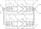
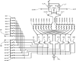
- Example 1 is shown in FIG.
- the operational amplifier circuit includes switches SW11 to SW14, switches SW11B to 14B, switches SW21 to 24, switches SW21B to 24B, four signal amplifier units having transistors M1, M2, M1B, and M2B, and a current output from the signal amplifier unit.
- the signal amplification means includes transistors MC1 and MC2, current sources IL_M and IL_P, and a tail current source ITAIL.
- Each signal amplification unit One circuit with the switches SW11, SW11B, SW21, SW21B and the transistor M1, One circuit is composed of the switches SW12, SW12B, SW22, SW22B and the transistor M2. One circuit with the switches SW13, SW13B, SW23, SW23B and the transistor M1B, The switches SW14, SW14B, SW24, and SW24B and the transistor M2B constitute one circuit.
- these signal amplification units will be named as signal amplification units 1 to 4, respectively.
- the switches SW11 and SW11B do not conduct at the same time. That is, when the switch SW11 is conductive, SW11B is in a cut-off state, and when the switch SW11B is conductive, SW11 is in a cut-off state.
- the first signal amplification unit is A state 1 in which the switch SW11 transmits a signal input to the positive-phase input terminal INP to the gate terminal of the transistor M1 and connects the drain terminal of the transistor M1 and the source terminal of the transistor MC1 via the SW21;
- the switch SW11B transmits the signal input to the negative-phase input terminal INM to the gate terminal of the transistor M1, and has two states of state 2 in which the drain terminal of the transistor M1 is connected to the source terminal of the transistor MC2 via the SW21B.
- the same operation is performed for the remaining second to fourth signal amplification units. That is, the signal input to the input terminal INP of the positive phase is amplified, the signal input to the input terminal INM opposite to the state 1 in which the output current is output to the source terminal of the transistor MC1, and the output current is amplified. Is output to the source terminal of the transistor MC2.
- the switches SW11 to SW14 and the switches SW11B to 14B perform an operation of modulating the input signal
- the switches SW21 to SW24 and the switches SW21B to 24B perform an operation of demodulating the input signal.
- the output of the signal amplification unit is a current, the addition of the output of each signal amplification unit can be easily performed by short-circuiting the output terminals of the signal amplification unit.
- the impedance of the source terminals of the MC1 and MC2 becomes low. This has the effect of reducing the voltage fluctuation at the output terminal of the circuit and can reduce the frequency characteristics and slew rate required for circuit operation.
- the source terminals of the transistors M1, M2, M1B, and M2B constituting the signal amplification unit are short-circuited to supply current from the tail current source ITAIL.
- the total output current of the signal amplification unit is limited by the amount of current of the tail current source.
- the ratio of the time during which each signal amplification unit is in the state 1 and the state 2 is preferably 50% to 50% from the viewpoint of the offset and 1 / f noise modulation operation. If the ratio deviates from this value, the effect of offset and 1 / f noise modulation is reduced.
- the drain terminals of the transistors MC1 and MC2 are connected to OUTM and OUTP, which are output terminals of opposite phase and positive phase, respectively.
- a common mode feedback circuit may be provided to adjust the current amount of the current source IL_M, IL_P or the tail current ITAIL.
- the transistors M1, M2, M1B, and M2B are made with the same device size and designed so that the same drain current flows in the same bias state.
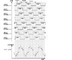
- FIG. 4 shows a timing chart showing the state of the signal amplification unit and the output voltage when the circuit of FIG. 3 is controlled so as to obtain the same effect as the conventional chopper stabilization technique.
- the portion not explicitly shown as state 1 in this timing chart is state 2.
- the combination of the states of the first to fourth signal amplification units in the modulation signal period TCHOP changes every TCHOP / 2.
- Specific combinations of states of the signal amplification units are two patterns of states 1, 1, 2, and 2 and states 2, 2, 1, 1, respectively.
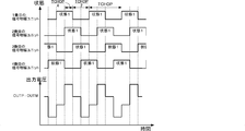
- FIG. 5 is a timing chart showing the state of the signal amplification unit and the output voltage when the state transition timing of the second and fourth signal amplification units is delayed by TCHOP / 4 using the present invention.
- the portion not explicitly shown as state 1 in this timing chart is state 2.
- the combination of the states of the first to fourth signal amplification units in the modulation signal cycle TCHOP changes every TCHOP / 4 time.
- the specific combinations of signal amplification unit states are states 1, 2, 2, 1 and states 1, 1, 2, 2 and states 2, 1, 1, 2 and states 2, 2, 1, 1 respectively. It is a pattern.
- the transistors M1, M2, M1B, and M2B shown in this embodiment may be any circuit that outputs a current according to an input signal.
- an amplifier circuit may be provided in front of the transistor M1, and a gate-grounded amplifier may be further provided between the drain terminal of the transistor M1 and SW21 and SW21B.
- Devices constituting the circuit are not limited to MOS transistors.
- the signal for controlling the switch does not need to be a periodic signal in principle, and may be a random signal.
- the random signal may or may not have periodicity.
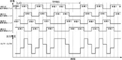
- FIG. 6 is a timing chart showing the switch state and output current when a pseudo-random signal is used as a signal for controlling the switch.
- the portion not explicitly shown as state 1 in this timing chart is state 2.
- the first signal amplification unit is controlled to be in state 1 when the pseudo-random signal of period TPRBS is HI, and the third signal amplification unit is controlled to be in state 1 when the pseudo-random signal is LOW.
- the second and fourth signal amplifying units control the states of the first and third signal amplifying units by delaying the state of TPRBS / 16, respectively.
- the number of signal amplification units shown in the first embodiment is not limited to four, and may be an even number of four or more.
- FIG. 7 shows a circuit diagram of the second embodiment.
- switches SW15 to SW18 switches SW15B to 18B, switches SW25 to 28, switches SW25B to 28B, and four signal amplification units having transistors M3, M4, M3B, and M4B are added.
- the added signal amplifying unit is composed of one switch SW15, SW15B, SW25, SW25B and a transistor M3.
- One circuit is composed of the switches SW16, SW16B, SW26, SW26B and the transistor M4.
- One circuit is composed of the switches SW17, SW17B, SW27, SW27B and the transistor M3B.
- the switches SW18, SW18B, SW28, SW28B and the transistor M4B are one circuit.
- these signal amplification units will be named as signal amplification units Nos. 5 to 8, respectively.
- the transistors M1 to M4 and M1B to M4B are made with the same device size and designed to allow the same drain current to flow in the same bias state.
- FIG. 8 is a timing chart showing the state and output voltage of the signal amplification unit according to the second embodiment. The portion not explicitly shown as state 1 in this timing chart is state 2.
- the operation timings of the second to eighth signal amplification units are sequentially delayed by TCHOP / 8 with respect to the operation state of the first signal amplification unit.
- the combination of the states of the first to eighth signal amplification units in the modulation signal period TCHOP changes every TCHOP / 8 time.
- Specific combinations of signal amplification unit states are states 1, 2, 2, 2, 2, 1, 1, 1, and States 1, 1, 2, 2, 2, 2, 1, 1, and States 1, 1, 1, 2, 2, 2, 2, 1, and States 1, 1, 1, 1, 2, 2, 2, 2, and States 2, 1, 1, 1, 1, 2, 2, 2, and States 2, 2, 1, 1, 1, 1, 2, 2, and States 2, 2, 2, 1, 1, 1, 1, 1, 1, 2, and States 2, 2, 2, 2, 1, 1, 1, 1, 1, 1, 2, and States 2, 2, 2, 2, 1, 1, 1, 1, 1, 2, and There are 8 patterns of states 2, 2, 2, 2, 1, 1, 1, 1.
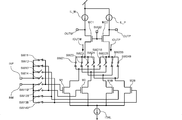
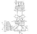
- FIG. 9 shows a third embodiment for removing the offset and 1 / f noise caused by the current sources IL_M and IL_P shown in the first and second embodiments.
- current sources IL_M and IL_P of the first embodiment there are four current source units including switches SW31 to 34, switches SW31B to 34B, and current sources IL5, IL6, IL5B, and IL6B.
- Each current source unit is One circuit with the switches SW31 and SW31B and the current source IL5, One circuit with the switches SW32 and SW32B and the current source IL6, One circuit with the switches SW33 and SW33B and the current source IL5B, The switches SW34 and SW34B and the current source IL6B are configured in one circuit.
- these current amplifying units are named as current source units 1 to 4, respectively.
- the first current source unit has two states: a state 3 in which the current of the current source IL5 is connected to the output terminal OUTM through the switch SW31, and a state 4 in which the current from the current source IL5 is connected to the output terminal OUTP through the switch SW31B.
- the same operation is performed for the remaining second to fourth current source units. That is, there are two states: a state 3 in which the currents of the current sources IL6, IL5B, and IL6B are connected to the output terminal OUTM, and a state 4 in which the currents of the current sources IL6, IL5B, and IL6B are connected to the output terminal OUTP.
- the output of the current source unit is a current
- the output of each current source unit can be easily added by short-circuiting the output terminals of the current source unit.
- the percentage of time that each current source unit is in state 3 and state 4 is preferably 50% to 50% from the viewpoint of the offset and 1 / f noise modulation operations. If the ratio deviates from this value, the effect of offset and 1 / f noise modulation is reduced.
- a common mode feedback circuit may be provided to adjust the current amount of the current source IL5, IL6, IL5B, IL6B or the tail current ITAIL. Good.
- the current sources IL5, IL6, IL5B, and IL6B are made with the same device size and designed to allow the same drain current to flow in the same bias state.
- FIG. 10 shows a timing chart of the state of the signal amplification unit and the current source unit.
- the portion not explicitly shown as state 1 in the timing chart of the state of the signal amplification unit is state 2
- the portion not explicitly shown as state 3 in the timing chart of the state of the current source unit is state 4.
- the timing at which the first to fourth signal amplification units are in states 1 and 2 is the same as the timing at which the first to fourth current source units are in states 3 and 4.
- the combinations of the states of the first to fourth signal amplification units in the modulation signal period TCHOP are four patterns as shown in the paragraph (0044).
- the specific combinations of the states of the first to fourth current source units are respectively There are four patterns of states 3, 4, 4, 3 and states 3, 3, 4, 4 and states 4, 3, 3, 4 and states 4, 4, 3, 3.
- the offsets and 1 / f noise of the current sources IL5, IL6, IL5B, and IL6B are modulated into waveforms that sequentially transition between the four states every time TCHOP / 4. The same effect as technology can be obtained.
- the number of current source units per state transition is reduced by half compared to the conventional chopper modulation technique, so that the finite frequency characteristics and slew rate of the signal amplification unit generated at the state transition timing are reduced.
- the glitch-shaped noise caused by the is reduced.
- FIG. 11 shows an example of a method for controlling so that the state transition of the signal amplification unit and the state transition of the current source unit do not occur simultaneously.
- the portion not explicitly shown as state 1 in the timing chart of the state of the signal amplification unit is state 2
- the portion not explicitly shown as state 3 in the timing chart of the state of the current source unit is state 4.
- FIG. 11 shows the operation timing of the first to fourth current source units in FIG. 10 delayed by TCHOP / 8.
- the paragraph (0079) describes that the operation timing is delayed by TCHOP / 8.
- the purpose is not to cause the state transition of the signal amplification unit and the current source unit at the same time.
- the amount of delay is not limited to TCHOP / 8.
- FIG. 12 shows an example in which the period of the state transition of the signal amplification unit and the state transition of the current source unit are different.
- the portion not explicitly shown as state 1 in the timing chart of the state of the signal amplification unit is state 2
- the portion not explicitly shown as state 3 in the timing chart of the state of the current source unit is state 4.
- TCHOP / 8 delays the operation timing of the first to fourth current source units in FIG. 10 by TCHOP / 8 and further sets the period of state transition to 2 TCHOP, which is twice TCHOP. Control is performed so that unit state transitions do not occur simultaneously.
- the period of state transition between the signal amplifying unit and the current source unit is the corner of 1 / f noise generated by the devices constituting each unit from the viewpoint of removing 1 / f noise as in the conventional chopper modulation technique. It is desirable that the frequency be higher than the frequency. On the other hand, if the modulation frequency is high, the operation speed required for the signal amplification unit and the current source unit increases, leading to an increase in area and an increase in current consumption. Therefore, the modulation frequency is preferably as low as possible.
- the modulation frequency of both can be set to different values as shown in FIG. Based on the ideas of paragraphs (0080) and (0081), the modulation frequency of both can be set so that the state transition of the signal amplification unit and the current source unit does not occur simultaneously.
- FIG. 12 shows an example in which the period of state transition of the signal amplification unit is shorter than the period of the current source unit, the magnitude relationship between these periods is not limited to the example of FIG.
- the period of state transition of the signal amplification unit may be longer than the period of the current source unit.
- the number of current source units is not limited to four, and may be M (M is an even number of 4 or more).
- the number N of signal amplification units and the number M of current source units need not be the same, and may be different values.
- the number of combinations of the states of the signal amplification units and the number of combinations of the states of the current source units need not be the same, and may be different.
- the number of combinations of the states of the signal amplification unit and the current source unit need not be more than 4 patterns. Any one of the numbers may be two patterns. Further, when the number of combinations of the states of the signal amplification units and the current source units is two patterns, the effect of reducing the number of signal amplification units per state transition shown in paragraphs (0046) and (0077) cannot be obtained. Are the effects of shifting the operation timing so that state transitions of the signal amplification unit and the current source unit shown in paragraphs (0080) and (0081) do not occur simultaneously, and the signal amplification unit and the current source unit shown in paragraph (0085) The effect of setting the modulation frequency to a different value can be obtained.
- Paragraphs (0038), (0057), and (0073) describe the case where the transistors or current sources constituting the signal amplification unit and the current source unit are made with the same device size and designed to allow the same drain current to flow in the same bias state.
- this is not limited to designing the current flowing through the signal amplification unit and the current source unit of the present invention to be equal. What is necessary is just to design so that the total value of the device size which outputs an electric current to the output terminal of a normal phase and an anti
- the first and third signal amplification units do not overlap in the state 1 state
- the second and fourth signal amplification units do not overlap in the state 1 state.
- the ratio of the device sizes of the signal amplification units in the state 1 and state 2 is always 3: 3.
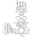
- FIG. 13 shows an example in which transistors MC3 and MC4 are added as signal amplification means to the circuit shown in the third embodiment, and a cascode current source is configured in combination with a current source unit.
- Transistors MC3 and MC4 are provided between the four current source units and the output terminals OUTM and OUTP, and BIAS2 is applied as the gate bias thereof.
- the operations of the signal amplification unit and the current source unit are the same as those in the third embodiment.
- the modification of the fourth embodiment shown in FIG. 13 has the same effect as the paragraphs (0030) and (0031) on the output terminal of the current source unit. That is, there is an effect that voltage fluctuations associated with modulation operation can be reduced, and frequency characteristics and slew rate required for circuit operation can be reduced.
- transistors MC1, MC2 and MC3, MC4 used as signal amplifying means are not necessarily required because the signal amplification effect is reduced depending on the load of the operational amplifier circuit.
- a folded cascode configuration can be obtained by modifying the circuit of the fourth embodiment. An embodiment is shown in FIG.
- current sources IL1, IL2, IL1B, and IL2B are respectively added to four signal amplification units, and the transistors MC1, MC2, MC3, and MC4 are replaced with transistors MC1B, MC2B, MC3B, and MC4B.
- Each signal amplification unit One circuit with the switches SW11, SW11B, SW21, SW21B, the transistor M1 and the current source IL1, One circuit is composed of the switches SW12, SW12B, SW22, SW22B, the transistor M2, and the current source IL2.
- the current source unit is the same as that of the fourth embodiment except that the direction of the output current of the current source differs depending on whether it is in the power supply direction or the ground direction.
- the operation of these current source units is the same as that of the fourth embodiment, except that the transistors MC3 and MC4 are replaced with MC3B and MC4B.
- FIG. 15 shows an embodiment in which a bandgap reference circuit is configured using the operational amplifier circuit of the fourth embodiment.
- transistors ML1, ML2, ML1B, and ML2B are used instead of the current sources IL5, IL6, IL5B, and IL6B in the circuit of FIG.
- the gate terminals of these transistors are connected to the OUTP terminal to convert the output from differential to single phase.
- the gate of the transistor MOUT is connected to the output terminal OUTM, and the drain is connected to the terminal BGROUT.
- resistors RBGR1, RBGR2, and RLPF are connected to the terminal BGROUT.
- resistors RBGR1 and RBGR2 are connected to input terminals INM and INP, respectively.
- the anode of D21 and one terminal of the resistor RBGR3 are connected to the input terminals INM and INP, respectively.
- the cathode of the diode D11 and the anode of D12 are connected, and the other terminal of the resistor RBGR3 is connected to the anode of the diode D11.
- the cathode of the diode D21 and the anode of D22 are connected, and the cathodes of the diodes D12 and D22 are connected to the ground terminal.
- the other terminal of the resistor RLPF is connected to the capacitor CLPF, and the other terminal of the capacitor CLPF is connected to the ground terminal to constitute a low-pass filter, and its output is a terminal LPFOUT.
- the offset and 1 / f noise of the transistors M11, M12, M11B, and M12B and the transistors ML1, ML2, ML1B, and ML2B are modulated, the offset voltage and 1 / f noise of the operational amplifier circuit appearing at the terminal BGROUT are reduced. .
- the modulated offset voltage and 1 / f noise can be reduced by the low-pass filter.
- ⁇ 28B Switches connected to the drains of transistors M1 ⁇ 4 and M1B ⁇ 4B IOUTP Current flowing in the current path of the positive phase output terminal IOUTM Current flowing in the current path of the negative phase output terminal TCHOP modulation signal period TPRBS pseudo-random signal period ITAIL tail current source IL_P current source IL_M current source IL5, 6 Current source IL5B, 6B Current source SW31 to 34 Switches SW31B to 34B connected to the current sources IL5, 6, IL5B, 6B SW31B to 34B Switches connected to the current sources IL5, IL5B, 6B ML1, 2 transistor ML1B, 2B transistor MC1 to 4 Transistor BIAS2 Bias terminal BIAS3 of transistors MC1 and MC2 Bias terminal of transistors MC3 and MC4 MC1B to 4B Transist
Landscapes
- Engineering & Computer Science (AREA)
- Power Engineering (AREA)
- Amplifiers (AREA)
Applications Claiming Priority (2)
| Application Number | Priority Date | Filing Date | Title |
|---|---|---|---|
| JP2014144598A JP6399486B2 (ja) | 2014-07-14 | 2014-07-14 | 演算増幅回路 |
| JP2014-144598 | 2014-07-14 |
Publications (1)
| Publication Number | Publication Date |
|---|---|
| WO2016009924A1 true WO2016009924A1 (ja) | 2016-01-21 |
Family
ID=55078420
Family Applications (1)
| Application Number | Title | Priority Date | Filing Date |
|---|---|---|---|
| PCT/JP2015/069681 Ceased WO2016009924A1 (ja) | 2014-07-14 | 2015-07-08 | 演算増幅回路 |
Country Status (2)
| Country | Link |
|---|---|
| JP (1) | JP6399486B2 (enExample) |
| WO (1) | WO2016009924A1 (enExample) |
Cited By (1)
| Publication number | Priority date | Publication date | Assignee | Title |
|---|---|---|---|---|
| US20210305953A1 (en) * | 2020-03-30 | 2021-09-30 | Apple Inc. | Amplifier circuit with distributed dynamic chopping |
Families Citing this family (2)
| Publication number | Priority date | Publication date | Assignee | Title |
|---|---|---|---|---|
| CN108781061B (zh) * | 2016-03-11 | 2022-04-08 | 株式会社索思未来 | 放大电路、接收电路以及半导体集成电路 |
| US11277108B1 (en) * | 2020-12-28 | 2022-03-15 | Analog Devices International Unlimited Company | Variable gain amplifiers with cross-couple switching arrangements |
Citations (4)
| Publication number | Priority date | Publication date | Assignee | Title |
|---|---|---|---|---|
| US4947135A (en) * | 1989-07-28 | 1990-08-07 | Motorola, Inc. | Single-ended chopper stabilized operational amplifier |
| JP2006310959A (ja) * | 2005-04-26 | 2006-11-09 | Nec Corp | 差動増幅器及び表示装置のデータドライバ並びに差動増幅器の駆動方法 |
| JP2009303121A (ja) * | 2008-06-17 | 2009-12-24 | Nec Electronics Corp | 演算増幅器回路、その演算増幅器回路を用いた液晶表示装置の駆動方法 |
| JP2014116713A (ja) * | 2012-12-07 | 2014-06-26 | Toyohashi Univ Of Technology | 差動増幅器およびこれを使用する信号増幅装置 |
Family Cites Families (1)
| Publication number | Priority date | Publication date | Assignee | Title |
|---|---|---|---|---|
| JPS6072406A (ja) * | 1983-09-29 | 1985-04-24 | Shimadzu Corp | 直流電圧増幅回路 |
-
2014
- 2014-07-14 JP JP2014144598A patent/JP6399486B2/ja active Active
-
2015
- 2015-07-08 WO PCT/JP2015/069681 patent/WO2016009924A1/ja not_active Ceased
Patent Citations (4)
| Publication number | Priority date | Publication date | Assignee | Title |
|---|---|---|---|---|
| US4947135A (en) * | 1989-07-28 | 1990-08-07 | Motorola, Inc. | Single-ended chopper stabilized operational amplifier |
| JP2006310959A (ja) * | 2005-04-26 | 2006-11-09 | Nec Corp | 差動増幅器及び表示装置のデータドライバ並びに差動増幅器の駆動方法 |
| JP2009303121A (ja) * | 2008-06-17 | 2009-12-24 | Nec Electronics Corp | 演算増幅器回路、その演算増幅器回路を用いた液晶表示装置の駆動方法 |
| JP2014116713A (ja) * | 2012-12-07 | 2014-06-26 | Toyohashi Univ Of Technology | 差動増幅器およびこれを使用する信号増幅装置 |
Non-Patent Citations (1)
| Title |
|---|
| I. AKITA ET AL.: "A 0.06mm2 14nV/?Hz Chopper Instrumentation Amplifier with Automatic Differential-Pair Matching", SOLID- STATE CIRCUITS CONFERENCE DIGEST OF TECHNICAL PAPERS (ISSCC), 2013, 19 February 2013 (2013-02-19), pages 178 - 179, XP032350526, DOI: doi:10.1109/ISSCC.2013.6487689 * |
Cited By (3)
| Publication number | Priority date | Publication date | Assignee | Title |
|---|---|---|---|---|
| US20210305953A1 (en) * | 2020-03-30 | 2021-09-30 | Apple Inc. | Amplifier circuit with distributed dynamic chopping |
| US11588455B2 (en) | 2020-03-30 | 2023-02-21 | Apple Inc. | Amplifier circuit with dynamic offset calibration |
| US11936352B2 (en) * | 2020-03-30 | 2024-03-19 | Apple Inc. | Amplifier circuit with distributed dynamic chopping |
Also Published As
| Publication number | Publication date |
|---|---|
| JP2016021668A (ja) | 2016-02-04 |
| JP6399486B2 (ja) | 2018-10-03 |
Similar Documents
| Publication | Publication Date | Title |
|---|---|---|
| TWI640168B (zh) | 低雜訊電路 | |
| US10110204B2 (en) | Low power buffer with gain boost | |
| KR102697683B1 (ko) | 스위치드 커패시터 입력 회로 및 스위치드 커패시터 앰프 및 스위치드 커패시터 전압 비교기 | |
| CN102273079A (zh) | 积分器电路及具备该积分器电路的δς调制器 | |
| JP6503663B2 (ja) | 差動増幅回路 | |
| CN111295840A (zh) | 用于模/数转换器的经减小噪声动态比较器 | |
| JP2010213042A (ja) | 増幅回路及びアナログ/デジタル変換回路 | |
| CN101692603A (zh) | 增益自举型c类反向器及其应用电路 | |
| CN104426523A (zh) | 具有减小的抖动的波形转换电路 | |
| WO2017014262A1 (ja) | アナログマルチプレクサコア回路及びアナログマルチプレクサ回路 | |
| JP6399486B2 (ja) | 演算増幅回路 | |
| US7777655B2 (en) | Wideband switched current source | |
| EP3228012B1 (en) | Load current compensation for analog input buffers | |
| JP2017526208A (ja) | 電流コーディングとサイズコーディングとを組み合わせることによって位相補間器の線形性を改善すること | |
| CN104731144B (zh) | 一种参考电压产生电路 | |
| CN107786185B (zh) | 相位内插器 | |
| JP2017523659A (ja) | 容量性要素を使用して位相補間器の線形性を改善すること | |
| JP4284360B2 (ja) | A/d変換器 | |
| CN103346794A (zh) | 数模转换器 | |
| US20190089318A1 (en) | Variable gain amplifier | |
| JP2015159513A (ja) | スイッチトキャパシタ回路、ad変換器 | |
| CN101286731B (zh) | 高速差动至单端信号转换电路 | |
| CN108665917A (zh) | 接收器及控制接收器的方法 | |
| US8823442B1 (en) | System and method of reducing magnitudes of kick-back voltages in a circuit that alternates a direction of current flow through a load | |
| CN101958715A (zh) | 音频数字模拟转换器 |
Legal Events
| Date | Code | Title | Description |
|---|---|---|---|
| 121 | Ep: the epo has been informed by wipo that ep was designated in this application |
Ref document number: 15822836 Country of ref document: EP Kind code of ref document: A1 |
|
| NENP | Non-entry into the national phase |
Ref country code: DE |
|
| 122 | Ep: pct application non-entry in european phase |
Ref document number: 15822836 Country of ref document: EP Kind code of ref document: A1 |