WO2016009911A1 - 垂直共振器型面発光レーザの製造方法 - Google Patents
垂直共振器型面発光レーザの製造方法 Download PDFInfo
- Publication number
- WO2016009911A1 WO2016009911A1 PCT/JP2015/069613 JP2015069613W WO2016009911A1 WO 2016009911 A1 WO2016009911 A1 WO 2016009911A1 JP 2015069613 W JP2015069613 W JP 2015069613W WO 2016009911 A1 WO2016009911 A1 WO 2016009911A1
- Authority
- WO
- WIPO (PCT)
- Prior art keywords
- layer
- substrate
- chamber
- oxidation
- current confinement
- Prior art date
- Legal status (The legal status is an assumption and is not a legal conclusion. Google has not performed a legal analysis and makes no representation as to the accuracy of the status listed.)
- Ceased
Links
Images






Classifications
-
- H—ELECTRICITY
- H01—ELECTRIC ELEMENTS
- H01S—DEVICES USING THE PROCESS OF LIGHT AMPLIFICATION BY STIMULATED EMISSION OF RADIATION [LASER] TO AMPLIFY OR GENERATE LIGHT; DEVICES USING STIMULATED EMISSION OF ELECTROMAGNETIC RADIATION IN WAVE RANGES OTHER THAN OPTICAL
- H01S5/00—Semiconductor lasers
- H01S5/10—Construction or shape of the optical resonator, e.g. extended or external cavity, coupled cavities, bent-guide, varying width, thickness or composition of the active region
- H01S5/18—Surface-emitting [SE] lasers, e.g. having both horizontal and vertical cavities
- H01S5/183—Surface-emitting [SE] lasers, e.g. having both horizontal and vertical cavities having only vertical cavities, e.g. vertical cavity surface-emitting lasers [VCSEL]
-
- H—ELECTRICITY
- H10—SEMICONDUCTOR DEVICES; ELECTRIC SOLID-STATE DEVICES NOT OTHERWISE PROVIDED FOR
- H10P—GENERIC PROCESSES OR APPARATUS FOR THE MANUFACTURE OR TREATMENT OF DEVICES COVERED BY CLASS H10
- H10P14/00—Formation of materials, e.g. in the shape of layers or pillars
- H10P14/60—Formation of materials, e.g. in the shape of layers or pillars of insulating materials
Definitions
- the present invention relates to a method for manufacturing a vertical cavity surface emitting laser.
- a vertical cavity surface emitting laser (VCSEL: Vertical Cavity Surface Emitting Laser) is a laser device that outputs laser light in a direction perpendicular to a substrate surface by forming an optical resonator in a direction perpendicular to the substrate surface.
- VCSEL Vertical Cavity Surface Emitting Laser
- a current confinement structure is formed in order to concentrate the current in the light emitting region.
- an opening structure formed by oxidizing the outer peripheral side of an AlAs (aluminum arsenic) layer is used as the current confinement structure.
- the oxidation of the AlAs layer is carried out by holding the substrate on which the laminate (object to be oxidized) processed into a mesa shape so that the AlAs layer is exposed on the side surface in heated steam at 400 to 500 ° C. Is executed.
- the temperature distribution in the substrate is preferably within ⁇ 1 ° C.
- Patent Document 1 A method described in Japanese Patent Application Laid-Open No. 2011-18876 (Patent Document 1) is known as a method for making the temperature distribution in the substrate uniform.
- the upper surface of the heat radiating plate on which the substrate is placed is processed into a spherical shape following the warp during the thermal oxidation of the substrate on which the oxidation target is formed.
- Patent Document 1 The method described in the above Japanese Unexamined Patent Publication No. 2011-18876 (Patent Document 1) has the following problems. First, since the amount of warpage of the substrate varies depending on the temperature of the substrate, it is difficult to accurately grasp the amount of warpage during heating oxidation. Further, the amount of warpage of the substrate varies depending on the structure of the epitaxial film formed on the substrate and the growth conditions thereof, and thus varies depending on the product type (model number). For this reason, in order to implement
- the present invention has been made in consideration of the above-described problems, and the object of the present invention is to form a current confinement layer by a heating steam oxidation method in the manufacture of a vertical cavity surface emitting laser. It is to equalize the temperature distribution in the substrate and the oxidation distribution of the object to be oxidized.
- the present invention provides a method for manufacturing a vertical cavity surface emitting laser, and includes a stacked body including first and second reflecting mirror layers, an active layer, and an oxidized layer serving as a current confinement structure on a substrate.
- the step of forming the current confinement structure includes a step of placing a substrate having a processed laminated body on a stage provided inside a chamber that can be hermetically sealed, and a pure structure outside the chamber.
- the method includes the steps of generating water vapor gas by heating pure water in a vacuum atmosphere, and supplying the water vapor gas by controlling the flow rate into a vacuum atmosphere chamber.
- the steam gas generated by heating pure water in a vacuum atmosphere is supplied as an oxidizing gas into the chamber, so that the oxidizing gas is blown using an inert gas such as nitrogen gas as a carrier.
- an inert gas such as nitrogen gas as a carrier.
- the diffusion efficiency of the gas is high as much as the inert gas does not exist, and the oxidizing gas can be supplied uniformly to the oxidation target layer of the laminate.
- the oxidizing gas is not strongly blown, it is possible to suppress the occurrence of a temperature drop of the substrate and the accompanying variation in temperature distribution, and the degree of progress of oxidation of the oxidized layer can be made uniform. Thereby, the oxidation distribution of the oxidation target can be made uniform.
- the stage includes a heating unit for heating the substrate and a support member for supporting the substrate at three points of the peripheral portion of the substrate.
- the contact area between the stage and the substrate can be minimized, and the amount of heat that escapes through the stage by heat conduction is minimized. Can be stopped. Also, since the heat conduction through the oxidizing gas is small because it is in a vacuum atmosphere, the radiant heat is dominant between the stage and the substrate, and the temperature distribution on the surface of the substrate due to the warpage of the substrate is uneven. Generation
- production etc. can be suppressed and it becomes possible to stabilize quality at a high level by equalizing the progress degree of oxidation of the layer to be oxidized of the laminate.
- the step of forming the current confinement structure further includes a step of confirming the progress of oxidation of the oxidation target layer of the stacked body by infrared rays from an observation window provided on the top surface of the chamber.
- the temperature distribution in the substrate and the oxidation distribution of the object to be oxidized are more uniform than in the prior art when the current confinement layer is formed by the heating oxidation method.
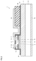
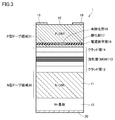
- FIG. 2 is a diagram schematically showing a cross-sectional structure along the line II-II in FIG. 1. It is the figure which expanded a part of FIG. It is a distribution map of Al composition of each layer of FIG.
- FIG. 5 is a cross-sectional view schematically showing a multilayer epitaxial film in a VCSEL manufacturing process. It is sectional drawing which shows typically formation of a mesa post structure in the manufacturing process of VCSEL. It is sectional drawing which shows typically the oxidation of the outer peripheral part of a current confinement layer in the manufacturing process of VCSEL. It is sectional drawing which shows typically formation of a moisture-proof film
- FIG. 1 is a plan view schematically showing the configuration of a VCSEL.
- FIG. 2 is a diagram schematically showing a cross-sectional structure along the line II-II in FIG.
- FIG. 3 is an enlarged view of a part of FIG. 2 and 3 are schematic diagrams, and the thickness of each layer in the drawings is not proportional to the actual thickness of the device. Also, the thicknesses of the layers in FIGS. 2 and 3 are not proportional to each other.
- the VCSEL 1 is disposed inside the substrate 10, the semiconductor multilayer reflector layers 11, 15, the clad layers 12, 14, the active layer 13, and the semiconductor multilayer reflector layer 15.
- the current confinement layer 16, the anode electrode layer 19, and the cathode electrode layer 20 are provided.
- a GaAs (gallium arsenide) semiconductor substrate exhibiting an N-type conductivity is used as the substrate 10.
- a cathode electrode layer (back electrode layer) 20 is formed on the back surface of the substrate 10.
- a non-doped GaAs substrate exhibiting semi-insulating properties may be used as the substrate 10.
- the cathode electrode layer 20 is formed on the surface of the DBR layer 11.
- a semiconductor multilayer reflector (DBR: Distributed Bragg Reflector) layer 11 made of a compound semiconductor having N-type conductivity is formed on the substrate 10.
- the DBR layer 11 includes, for example, a structure in which Al 0.15 Ga 0.85 As and Al 0.9 Ga 0.1 As are alternately stacked with an optical film thickness ⁇ / 4.
- Si silicon
- Si is doped to give an N-type conductivity, and its concentration is, for example, 2 to 3 ⁇ 10 18 [cm ⁇ 3 ].
- Si coordinates to a Ga (Al) site and easily becomes a donor.
- Al X Ga (1-X) As (aluminum, gallium, arsenic) is a mixed crystal semiconductor of GaAs and AlAs.
- Al composition (X) when the Al composition (X) is not specified, it may be described as AlGaAs.
- the active region for generating laser light is formed on the DBR layer 11.
- the active region includes the clad layers 12 and 14 and the active layer 13 having an optical gain sandwiched between the clad layers 12 and 14.
- a multiple quantum well (MQW) in which a quantum well layer and a barrier layer are stacked in multiple layers is formed.
- the active layer 13 is a non-doped region where impurities are not introduced.
- the cladding layers 12 and 14 can be non-doped or partially doped depending on the design of the resistance value of the device.
- a part of the cladding layers 12 and 14 in contact with the N-type and P-type DBR layers 11 and 15 is doped with an impurity having the same conductivity type as that of the adjacent DBR layers 11 and 15.
- An upper DBR layer 15 made of a compound semiconductor having a P-type conductivity is formed on the active region.
- the upper DBR layer 15 constitutes an optical resonator together with the lower DBR layer 11.
- the DBR layer 15 is made of, for example, Al 0.15 Ga 0.85 As and Al 0.9 Ga 0.1 As each having an optical film thickness of ⁇ / 4 ( ⁇ ). (Represents the wavelength of the laser beam) and includes an alternately stacked structure.
- C carbon
- concentration is, for example, 2 to 3 ⁇ 10 18 [cm ⁇ 3 ]. C is easily coordinated to the As site and becomes an acceptor.
- the conductivity type may be reversed, the substrate 10 may be a P-type semiconductor substrate, the lower DBR layer 11 may be P-type, and the upper DBR layer 15 may be N-type.
- the first and second conductivity types are described, one of the first and second conductivity types is P-type, and the other is N-type.
- a current confinement layer 16 is formed in a part of the upper DBR layer 15 to efficiently inject current into the active region and bring about a lens effect.
- the current confinement layer 16 has an unoxidized portion 18 at the central portion and an oxidized portion 17 of a substantially insulator around the central portion.
- a moisture-proof insulating film 21 (also referred to as a moisture-resistant film) is formed on an epitaxial multilayer film having a mesa post structure. An opening is formed in the insulating film 21 above the mesa post so that the surface of the DBR layer 15 is exposed.
- An anode electrode layer 19 (ring electrode layer) is connected to the exposed surface of the DBR layer 15.
- a pad electrode 23 for bonding is connected to the anode electrode layer 19.
- a polyimide pattern 22 is provided between the pad electrode 23 and the DBR layer 11 in order to reduce parasitic capacitance.
- Al composition distribution 4 is a distribution diagram of the Al composition of each layer in FIG.
- the vertical axis of FIG. 4 indicates the Al content (X) of Al X Ga (1-X) As, and the horizontal axis indicates the depth direction of the VCSEL in arbitrary units (AU).
- a low refractive index layer having a high Al content and a high refractive index layer having a low Al content are alternately laminated.
- the region adjacent to the cladding layers 12 and 14 in the DBR layers 11 and 15 corresponds to the first low refractive index layer.
- the current confinement layer 16 is formed at a position farthest from the active layer 13 in the first low refractive index layer of the DBR layer 15.
- the current confinement layer 16 may be disposed on a lower layer side (for example, a position adjacent to the clad layer 14) in the first low refractive index layer.
- the P-type doped region 31 extends from the DBR layer 15 to a part of the cladding layer 14.
- the current confinement layer 16 is formed inside the first low-refractive index layer constituting the DBR layer 15, but may be arranged closer to the active layer 13 such as the inside of the cladding layer 14. Is possible. Therefore, more generally speaking, the current confinement layer 16 is disposed in the DBR layer 15 or between the DBR layer 15 and the active layer 13. Alternatively, the current confinement layer 16 can be disposed on the substrate 10 side with respect to the active layer 13, and may be disposed inside the DBR layer 11 or between the DBR layer 11 and the active layer 13.
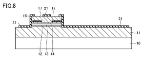
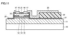
- FIGS. 5 to 11 are cross-sectional views schematically showing a VCSEL manufacturing process.
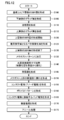
- FIG. 12 is a flowchart showing a VCSEL manufacturing process.
- a method for manufacturing the VCSEL 1 shown in FIGS. 1 to 4 will be described with reference to FIGS.
- multilayer epitaxial films 11 to 16 are formed on a semiconductor substrate 10 (here, an N-type GaAs substrate).
- a method such as MOCVD (Metal Organic Chemical Vapor Deposition) or MBE (Molecular Beam Epitaxy) is suitable.
- the DBR layer 11 showing the N-type conductivity is first formed on the GaAs substrate 10 (step S100 in FIG. 12).
- the DBR layer 11 is formed in 30 to 40 layers with a pair of optical film thicknesses such that the high refractive region and the low refractive region are each ⁇ / 4.
- about 2 ⁇ 10 18 [cm ⁇ 3 ] is introduced with Si as an impurity.
- an active layer 13 including a quantum well (QW) is formed on the N-type DBR layer 11 so as to be sandwiched between the cladding layers 12 and 14 (steps S105 to S115 in FIG. 12).
- the thickness and material of the active layer 13 and the cladding layers 12 and 14 can be appropriately adjusted according to the oscillation wavelength.
- GaAs can be used as the material of the active layer 13 and the oscillation wavelength can be adjusted to 850 nm.
- P-type DBR layers 15 and 15A are formed on the cladding layer 14 (steps S120 to S130 in FIG. 12). Similarly to the N-type DBR layer 11, the P-type DBR layers 15 and 15A are formed to have about 20 layers with a pair of optical film thicknesses such that the high refractive region and the low refractive region are each ⁇ / 4.
- about 2 ⁇ 10 18 [cm ⁇ 3 ] is introduced with C as an impurity.
- an oxidized layer to be the current confinement layer 16 is formed in the first low refractive index layer in contact with the cladding layer.
- step S125 in FIG. 12 then, by increasing the Al composition X 0.95 or more, Al X Ga (1-X) as layer as the layer to be oxidized (where 0 .95 ⁇ X ⁇ 1) is formed while introducing C (carbon) of about 2 to 3 ⁇ 10 18 [cm ⁇ 3 ] (step S125 in FIG. 12).
- the layer to be oxidized that should become the current confinement layer 16 is distorted due to volume shrinkage during the oxidation treatment, it is desirable that the layer be 40 nm or less in order to suppress the influence of the strain.
- the oxidized layer may be formed at a position near the upper layer or at a position near the lower layer in the first low refractive index layer.
- the epitaxial multilayer film (laminated body) formed on substrate 10 as described above is processed into a mesa post pattern of, for example, ⁇ 30 ⁇ m to form a current confinement structure (step S135 in FIG. 12).
- the mesa post pattern is formed by photolithography and dry etching techniques. The dry etching needs to be performed until at least the side surface of the oxidized layer to be the current confinement layer 16 is exposed. In the case of FIG. 6, the dry etching is performed to a depth at which the surface of the lower DBR layer 11 is exposed.
- the substrate with the epitaxial multilayer film processed into the mesa post pattern is heated to 450 ° C. or higher in a water vapor atmosphere, so that the oxidized film to be the current confinement layer 16 is changed to its outer peripheral portion.
- the oxidation portion 17 is formed by selectively advancing oxidation from (step S140 in FIG. 12). The oxidation time is adjusted so that the unoxidized portion 18 in the central portion becomes ⁇ 10 ⁇ m.
- the cross-sectional shape of the mesa post pattern and the shape of the current confinement layer 16 are not particularly limited, and may be a square or a rectangle other than a circle.
- a silicon nitride film or a silicon oxide film is formed as moisture-resistant film 21 (step S145 in FIG. 12).
- a technique such as CVD or sputtering can be applied.
- an opening for the contact electrode layer is formed by photolithography and dry etching (step S150 in FIG. 12).
- a P-type contact electrode layer (anode electrode layer) 19 is formed in the opening at the top of the mesa post, for example, by photolithography and vapor deposition (step S155 in FIG. 12).
- a laminated film made of Ti (titanium), Pt (platinum), and Au (gold) can be used.
- polyimide pattern 22 is formed for the purpose of capacity reduction under pad electrode 23 (step S160 in FIG. 12).
- pad electrode 23 connected to P-type contact electrode layer 19 is formed by, for example, photolithography and sputtering film formation (step S165 in FIG. 12).
- the back electrode layer 20 is formed (step S170 in FIG. 12).
- the back electrode layer 20 for example, a laminated film made of Au, Ge, and Ni can be used.
- the VCSEL 1 is completed by performing an annealing process (step S175 in FIG. 12) for making ohmic contact between the electrode layers 19 and 20 and the semiconductor layer.
- step S140 in FIG. 12 a method for forming a current confinement layer by heating steam oxidation
- FIG. 13 is a cross-sectional view schematically showing the configuration of the oxidation furnace.
- an oxidation furnace 150 includes a chamber 101 that can be hermetically sealed, and a stage 102 on which a substrate 110 having a processed stacked body is placed. .
- the stage 102 is provided with a heating unit (not shown) such as a heater for heating the substrate.
- the stage 102 is fixed in the chamber 101 by a fixing member 129.
- the heating unit include a heating mechanism using a resistance heater or an infrared lamp heater, but are not particularly limited.
- An oxidizing gas supply pipe 105 is provided on the wall surface of the chamber 101. After the chamber 101 is evacuated by evacuation of the pump 126, water vapor gas is supplied into the chamber 101 from the supply port 151 as an oxidizing gas.
- the oxidizing gas supply unit 120 is provided outside the chamber 101 and includes at least an oxidizing gas supply pipe 105, a pump 126, valves 121a to 121d, a pure water tank 122, ribbon heaters 123 and 124, and a controller 125. Steam gas is supplied as an oxidizing gas from the supply port 151 of the oxidizing gas supply pipe 105 of the oxidizing gas supply unit 120 into the chamber 101.
- the oxidation furnace 150 further includes a control unit 140 that controls operations of a heating unit provided in the stage 102, valves 121a to 121d, ribbon heaters 123 and 124, a controller 125, a pump 126, an infrared microscope 108, and the like.
- the control unit 140 is configured based on a computer.
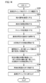
- FIG. 14 is a flowchart showing the procedure of the heating steam oxidation step (step S140 in FIG. 12). Of the steps in FIG. 14, steps S 205 to S 240 can be executed under the control of the control unit 140.
- step S ⁇ b> 200 the valve 121 b is opened and the pump 126 is used.
- the inside of the pure water tank 122 is evacuated by sucking the air inside the tube (step S205).
- the pure water stored in the pure water tank 122 is heated by the ribbon heater 123 to generate water vapor gas (step S210).
- the chamber 121 is evacuated by closing the valve 121b and opening the valve 121a (step S215). And after heating the board
- each valve described above is summarized in Table 1 for each procedure.
- Table 1 the valve 121b is “closed” at the start of pure water heating. This is because the valve 121b at the start of pure water heating is once the inside of the pure water tank 122 is in a vacuum state. This is because it may be closed.
- the flow rate of the water vapor gas is adjusted (flow rate control) by the controller 125.
- flow rate control In order to prevent condensate (liquefaction of water vapor gas), it is desirable to provide a ribbon heater 124 at an important point.
- the layer to be oxidized on the substrate 110 is oxidized from the surroundings by the water vapor gas induced into the chamber 101. Since the chamber 101 is in a vacuum state, heat transfer due to convection hardly occurs. By keeping the gap between the stage 102 and the substrate 110 around several millimeters, the heat transfer by convection becomes smaller. As a result, the heat transfer due to radiation accounts for the majority, so the temperature distribution on the surface of the substrate 110 can be easily achieved without depending on the temperature distribution on the surface of the stage 102, the warpage of the substrate 110, the flatness of the surface of the stage 102, or the like. It becomes possible to make uniform.
- the observation window 113 is provided on the top surface of the chamber 101, since heat transfer due to convection hardly occurs, the temperature distribution of the substrate 110 can be obtained even when the stage 102 and the observation window 113 are brought close to each other. This variation does not occur. Further, since the chamber 101 is in a vacuum state, oxidative gas convection does not occur, and the heat of the substrate 110 is less likely to escape from the observation window 113. That is, since the substrate 110 may be disposed close to the observation window 113, the progress of oxidation of the substrate 110 can be confirmed from the observation window 113 via the infrared microscope 108 even during the oxidation process ( Step S230). Further, since it is not necessary to provide a mechanism for moving the stage 102 up and down, the cost can be reduced and the oxidation time as a whole can be shortened.
- step S235 When the predetermined oxidation time has elapsed (or when the predetermined amount of oxidation has been reached), the supply of water vapor gas is stopped (step S235). Thereafter, the substrate 110 is cooled to near room temperature (step S240) and taken out from the oxidation furnace chamber 159 (step S245).
- stage 102 of the oxidation apparatus preferably includes a support member that supports substrate 110 at three points on the outer peripheral portion of substrate 110.
- the contact area between the stage 102 and the substrate 110 can be minimized.
- the heating of the substrate 110 is dominated by the heat transfer by radiation from the stage 102 to the substrate 110 rather than the heat conduction by the contact between the stage 102 and the substrate 10.
- the temperature distribution of the substrate 110 can be made uniform, and stable oxidation can be ensured.
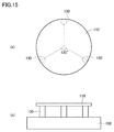
- FIG. 15 is a cross-sectional view schematically showing an enlarged main part of the stage 102 shown in FIG.
- FIG. 15A is a plan view showing the substrate 110 placed on the stage 102
- FIG. 15B is a front view showing the substrate 110 placed on the stage 102.
- the substrate 110 includes three support members 130 that support the substrate 110 at three points in the peripheral portion. Since the planar shape of the substrate 110 is circular, it is preferable to provide the three support members 130 at equiangular intervals at the peripheral portion, that is, so that the central angles formed by the three support members 130 are 120 degrees. This is because the substrate 110 can be stably supported by providing the support members 130 at equal angular intervals.
- the temperature distribution on the surface of the substrate 110 does not vary due to the warp generated in the substrate 110, and the oxidation can proceed uniformly.
- the oxidizing gas is sprayed using an inert gas such as nitrogen gas as a carrier.
- an inert gas such as nitrogen gas as a carrier.
- the diffusion efficiency of the gas is high as much as the inert gas does not exist, and the oxidizing gas can be supplied uniformly to the oxidation target layer of the laminate.
- the oxidizing gas is not strongly blown, it is possible to suppress the occurrence of a temperature drop of the substrate and the accompanying variation in temperature distribution, and the degree of progress of oxidation of the oxidized layer can be made uniform. Thereby, the oxidation distribution of the oxidation target can be made uniform.
- the stacked body including the DBR layers 11 and 15, the cladding layers 12 and 14, the active layer 13, and the oxidized layer to be the current confinement layer 16 is processed into a mesa post shape.
- the laminate may be processed into a recess structure.
- an oxidation portion is formed so as to surround an unoxidized portion by the progress of oxidation from the side surface of the oxidized layer that should become the current confinement layer 16.
Landscapes
- Physics & Mathematics (AREA)
- Condensed Matter Physics & Semiconductors (AREA)
- General Physics & Mathematics (AREA)
- Electromagnetism (AREA)
- Optics & Photonics (AREA)
- Semiconductor Lasers (AREA)
Abstract
垂直共振器型面発光レーザの製造方法では、被酸化層を含む積層体を加工することによって被酸化層の側面を露出した後に、加熱水蒸気酸化工程によって電流狭窄層が形成される。加熱水蒸気酸化工程は、内部を気密にすることが可能なチャンバ(101)の内部に設けられたステージ(102)に、加工後の積層体を有する基板(110)を載置するステップと、チャンバ(101)の外部の純水漕(122)において、真空雰囲気中で純水を加熱することにより水蒸気ガスを生成するステップと、水蒸気ガスを、真空雰囲気としたチャンバ(101)内へ流量制御して供給するステップとを含む。
Description
この発明は、垂直共振器型面発光レーザの製造方法に関する。
垂直共振器型面発光レーザ(VCSEL:Vertical Cavity Surface Emitting Laser)は、基板面と垂直方向に光共振器を形成することにより、基板面と垂直方向にレーザ光を出力するレーザ装置である。通常、VCSELでは、電流を発光領域に集中させるために電流狭窄構造が形成される。
電流狭窄構造として多くの場合、AlAs(アルミニウム・ヒ素)層の外周側を酸化することによって形成された開口構造が利用される。具体的には、AlAs層が側面に露出するようにメサ型に加工した積層体(酸化対象物)が形成された基板を、400~500℃の加熱水蒸気中に保持することによってAlAs層の酸化が実行される。この場合、基板内の温度分布は±1℃以内であることが望ましい。
基板内の温度分布を均一化させる方法として、特開2011-18876号公報(特許文献1)に記載された方法が知られている。この文献の方法では、酸化対象物が形成された基板の加熱酸化時における反りに倣って、基板が載置される放熱板の上部表面が球面状に加工される。
上記の特開2011-18876号公報(特許文献1)に記載の方法には以下の問題がある。まず、基板の反り量は、基板の温度によって異なるので、加熱酸化時の反り量を正確に把握することは難しい。さらに、基板の反り量は基板上に形成されるエピタキシャル膜の構造やその成長条件によっても異なるため、製品の種類(型番)ごとに異なる大きさとなる。このため、上記の文献の方法を実現するためには、製品の種類ごとに上部表面の曲率が異なる放熱板を準備する必要があることになり、容易でない。
この発明は、上記の問題を考慮してなされたものであり、その目的は、垂直共振器型面発光レーザの製造において、加熱水蒸気酸化の方法によって電流狭窄層を形成する際に、従来よりも基板内の温度分布および酸化対象物の酸化分布を均一化することである。
この発明は一局面において垂直共振器型面発光レーザの製造方法であって、第1および第2の反射鏡層、活性層、ならびに電流狭窄構造となる被酸化層を含む積層体を基板上に形成するステップと、少なくとも被酸化層の側面が露出するように、積層体をメサ状に加工するステップと、積層体をメサ状に加工した後に、被酸化層を側面から酸化することによって電流狭窄構造を形成するステップとを備える。上記の電流狭窄構造を形成するステップは、内部を気密にすることが可能なチャンバの内部に設けられたステージに、加工後の積層体を有する基板を載置するステップと、チャンバの外部の純水漕において、真空雰囲気中で純水を加熱することにより水蒸気ガスを生成するステップと、水蒸気ガスを、真空雰囲気としたチャンバ内へ流量制御して供給するステップとを含む。
上記の製造方法によれば、真空雰囲気中で純水を加熱することにより生成した水蒸気ガスを酸化ガスとしてチャンバ内に供給するので、窒素ガスのような不活性ガスをキャリアとして酸化ガスを吹き付ける従来の方法と比較して、不活性ガスが存在しない分だけガスの拡散効率が高く、積層体の被酸化層に均一に酸化ガスを供給することができる。また、酸化ガスを強く吹き付けることがないので、基板の温度低下の発生、それに伴う温度分布のバラツキの発生等を抑制することができ、被酸化層の酸化の進行度合いを均一化できる。これにより、酸化対象物の酸化分布を均一化できる。
好ましくは、ステージは、基板を加熱するための加熱部と、基板の周縁部分の3点において基板を支持する支持部材とを含む。
上記構成では、基板の周縁部分の3点において、支持部材により基板を支持するので、ステージと基板との接触面積を最小にすることができ、熱伝導によりステージを介して逃げる熱量を最小限に止めることができる。また、真空雰囲気中であるので、酸化ガスを介した熱伝導も小さいことから、ステージと基板との間は輻射熱が支配的であり、基板の反りに起因する基板の表面における温度分布のバラツキの発生等を抑制することができ、積層体の被酸化層の酸化の進行度合いを均一化することにより、品質を高いレベルで安定させることが可能となる。
好ましくは、上記の電流狭窄構造を形成するステップは、チャンバの天面に設けられた観察窓から、赤外線により、積層体の被酸化層の酸化の進行度合いを確認するステップをさらに備える。
上記構成では、チャンバ内が真空雰囲気であるため、酸化ガスの対流が生じず、天面に備えた観察窓から熱が逃げにくい。したがって、ステージに載置されている基板の表面における温度分布のバラツキを回避することができる。また、酸化の進行時と進行度合いの観察時とでステージと観察窓との距離を変更するためにステージを上下動させる機構等を備える必要もなく、全体として製造コストの低減を図ることが可能となる。
したがって、この発明によれば、直共振器型面発光レーザの製造において、加熱酸化の方法によって電流狭窄層を形成する際に、従来よりも基板内の温度分布および酸化対象物の酸化分布を均一化することができる。
以下、実施の形態について図面を参照して詳しく説明する。以下では、VCSELの構成およびその製造方法について説明した後、この発明の特徴である酸化方法について詳しく説明する。なお、以下の説明において、同一または相当する部分には同一の参照符号を付して、その説明を繰返さない場合がある。
[VCSELの構成]
図1は、VCSELの構成を模式的に示す平面図である。図2は、図1のII-II線に沿った断面構造を模式的に示す図である。図3は、図2の一部を拡大した図である。なお、図2および図3に示す断面図は模式図であって、図中の各層の厚みは実際のデバイスの厚みと比例関係にない。また、図2と図3の各層の厚みも互いに比例関係にない。
図1は、VCSELの構成を模式的に示す平面図である。図2は、図1のII-II線に沿った断面構造を模式的に示す図である。図3は、図2の一部を拡大した図である。なお、図2および図3に示す断面図は模式図であって、図中の各層の厚みは実際のデバイスの厚みと比例関係にない。また、図2と図3の各層の厚みも互いに比例関係にない。
図1~図3を参照して、VCSEL1は、基板10と、半導体多層膜反射鏡層11,15と、クラッド層12,14と、活性層13と、半導体多層膜反射鏡層15の内部に設けられた電流狭窄層16と、アノード電極層19と、カソード電極層20とを含む。
この実施の形態では、基板10としてN型の導電型を示すGaAs(ガリウム・ヒ素)半導体基板が用いられる。基板10の裏面にカソード電極層(裏面電極層)20が形成される。なお、図1~図3の場合と異なるが、基板10として半絶縁性を示すノンドープのGaAs基板を用いることもできる。この場合には、カソード電極層20は、DBR層11の表面に形成される。
基板10上には、N型の導電型を示す化合物半導体で構成された半導体多層膜反射鏡(DBR:Distributed Bragg Reflector)層11が形成される。DBR層11は、たとえばAl0.15Ga0.85AsとAl0.9Ga0.1Asとを光学膜厚λ/4ずつ交互に積層した構造を含む。N型の導電型を与えるためにSi(シリコン)がドーピングされており、その濃度は、たとえば2~3×1018[cm-3]である。SiはGa(Al)サイトに配位してドナーになりやすい。
なお、AlXGa(1-X)As(アルミニウム・ガリウム・ヒ素)は、GaAsとAlAsとの混晶半導体であり、Al組成(X)が高いほどエネルギーギャップが広く、屈折率は低くなる。Al組成(X)に応じて格子定数がほとんど変化しないために、あらゆるAl組成(X)のAlXGa(1-X)As膜をGaAs基板上にエピタキシャル成長可能である。この明細書では、Al組成(X)を特定しない場合には、AlGaAsと記載する場合がある。
DBR層11の上に、レーザ光を発生する活性領域が形成される。活性領域は、クラッド層12,14と、クラッド層12,14に挟まれた光学利得を有する活性層13とによって構成される。活性層13には、量子井戸層と障壁層とを多重に積層した多重量子井戸(MQW:Multiple Quantum Well)が形成される。活性層13は、不純物を導入しないノンドープ領域である。
クラッド層12,14は、デバイスの抵抗値の設計に応じて、ノンドープにすることも部分的にドープすることもできる。本実施の形態では、N型およびP型DBR層11,15に接するクラッド層12,14の一部に、隣接するDBR層11,15と同じ導電型の示す不純物をドープしている。
活性領域の上に、P型の導電型を示す化合物半導体で構成された上層側のDBR層15が形成される。上層側のDBR層15は、下層側のDBR層11とともに光共振器を構成する。DBR層15は、電流狭窄層16を除いて、下層側(基板側)のDBR層11と同様に、たとえばAl0.15Ga0.85AsとAl0.9Ga0.1Asとを光学膜厚λ/4ずつ(λはレーザ光の波長を表す)交互に積層した構造を含む。P型の導電型を与えるために、C(カーボン)がドーピングされており、その濃度は、たとえば2~3×1018[cm-3]である。CはAsサイトに配位してアクセプタになりやすい。
ここで、導電型を上記と逆にして、基板10をP型半導体基板にし、下層側のDBR層11の導電型をP型にし、上層側のDBR層15の導電型をN型としてもよい。なお、この明細書において第1および第2の導電型と記載した場合には、第1および第2の導電型のうち一方がP型であり、他方がN型である。
さらに、上層側のDBR層15の一部に、活性領域に効率よく電流を注入し、レンズ効果をもたらす電流狭窄層16が形成される。図3に示すように、電流狭窄層16は中心部分の未酸化部18とその周囲のほぼ絶縁体の酸化部17とを有する。この構造は、電流狭窄層16となるべき被酸化層を0.95≦X≦1のAlXGa(1-X)Asで形成し(X=1の場合、すなわちAlAsを含む)、被酸化層を含むエピタキシャル多層膜をメサポスト形状に加工した後に、加熱水蒸気雰囲気下で被酸化層を周囲から選択的に酸化させることによって得られる。中心部分の未酸化部18のみが電流経路となるので、活性領域に効率よく電流を注入できる。
図1、図2に示すようにメサポスト構造を有するエピタキシャル多層膜上には、防湿用の絶縁膜21(耐湿膜とも称する)が形成されている。メサポスト上部の絶縁膜21にはDBR層15の表面が露出するような開口が形成される。露出したDBR層15の表面には、アノード電極層19(リング電極層)が接続される。アノード電極層19にはボンディング用のパッド電極23が接続される。パッド電極23とDBR層11との間には、寄生容量を低減するためにポリイミドパターン22が設けられている。
[Al組成分布]
図4は、図3の各層のAl組成の分布図である。図4の縦軸はAlXGa(1-X)AsのAl含有量(X)を示し、横軸はVCSELの深さ方向を任意単位(AU)で示す。X=0の場合はGaAsを意味し、X=1の場合はAlAsを意味する。
図4は、図3の各層のAl組成の分布図である。図4の縦軸はAlXGa(1-X)AsのAl含有量(X)を示し、横軸はVCSELの深さ方向を任意単位(AU)で示す。X=0の場合はGaAsを意味し、X=1の場合はAlAsを意味する。
図4を参照して、DBR層11,15では、Al含有量が多い低屈折率層とAl含有量が少ない高屈折率層とが交互に積層されている。DBR層11,15のうちクラッド層12,14に隣接する領域が第1番目の低屈折率層に相当する。図4の場合、電流狭窄層16は、DBR層15の第1番目の低屈折率層内で、最も活性層13から離間した位置に形成される。電流狭窄層16を第1番目の低屈折率層内でより下層側(たとえば、クラッド層14に隣接する位置)に配置してもよい。P型ドープ領域31は、DBR層15からクラッド層14の一部にまで達する。
なお、電流狭窄層16は、DBR層15を構成する第1番目の低屈折率層の内部に形成されていたが、クラッド層14の内部など、より活性層13に近い位置に配置することも可能である。したがって、より一般的に言えば、電流狭窄層16は、DBR層15の内部またはDBR層15と活性層13との間に配置される。あるいは、電流狭窄層16は、活性層13よりも基板10側に配置することも可能であり、DBR層11の内部またはDBR層11と活性層13との間に配置してもよい。
[VCSELの作製プロセス]
図5~図11は、VCSELの作製プロセスを模式的に示す断面図である。図12は、VCSELの作製プロセスを示すフローチャートである。以下、図5~図12を参照して、図1~図4で示したVCSEL1の作製方法について説明する。
図5~図11は、VCSELの作製プロセスを模式的に示す断面図である。図12は、VCSELの作製プロセスを示すフローチャートである。以下、図5~図12を参照して、図1~図4で示したVCSEL1の作製方法について説明する。
図5を参照して、半導体基板10(ここでは、N型GaAs基板)上に、多層のエピタキシャル膜11~16を形成する。エピタキシャル膜の形成はMOCVD(Metal Organic Chemical Vapor Deposition)またはMBE(Molecular Beam Epitaxy)などの手法が好適である。
具体的に、GaAs基板10上に、まずN型の導電型を示すDBR層11を形成する(図12のステップS100)。DBR層11は、高屈折領域、低屈折領域がそれぞれλ/4となる光学膜厚を1ペアとして、30~40層形成する。高屈折材料としてAlXGa(1-X)AsでX=0.1程度のものが、低屈折材料としてAlXGa(1-X)AsでX=0.9程度のものが利用できる。N型の導電型を得るために、Siを不純物として2×1018[cm-3]程度導入する。
次にN型DBR層11の上に、クラッド層12,14に挟まれた形で量子井戸(QW:Quantum Well)を含む活性層13を形成する(図12のステップS105~S115)。活性層13およびクラッド層12,14は、発振波長に応じて適宜、その膜厚および材料を調整することができる。たとえば、活性層13の材料としてはGaAsを利用し、発振波長が850nmとなるように調整できる。
次にクラッド層14の上に、P型DBR層15,15Aを形成する(図12のステップS120~S130)。P型DBR層15,15AもN型DBR層11と同様に、高屈折領域および低屈折領域がそれぞれλ/4となる光学膜厚を1ペアとして20層程度形成する。高屈折材料としてAlXGa(1-X)AsでX=0.1程度のものが、低屈折材料としてAlXGa(1-X)AsでX=0.9程度のものが利用できる。P型の導電型を得るために、Cを不純物として2×1018[cm-3]程度導入する。
ただし、図1~図4に示す構造の場合には、クラッド層14に接する第1番目の低屈折率層に電流狭窄層16となるべき被酸化層が形成される。具体的には、例えば、クラッド層14の上にAlXGa(1-X)As層15A(ただし、X=0.65)を2~3×10¹⁸[cm-3]程度のC(カーボン)を導入しながら形成し(図12のステップS120)、次に、Al組成Xを0.95以上に増加させることにより、被酸化層としてAlXGa(1-X)As層(ただし、0.95≦X≦1)を2~3×10¹⁸[cm-3]程度のC(カーボン)を導入しながら形成する(図12のステップS125)。
電流狭窄層16となるべき被酸化層は、酸化処理を行うときの体積収縮により歪が発生するので、歪の影響を抑えるために40nm以下にすることが望ましい。この被酸化層は、図4で説明したように、第1番目の低屈折率層中で上層寄りの位置に形成しても、下層寄りの位置に形成してもよい。
図6を参照して、上記のように基板10上に形成したエピタキシャル多層膜(積層体)を、電流狭窄構造を形成するため、たとえばφ30μmのメサポストパターンに加工する(図12のステップS135)。メサポストパターンは、フォトリソグラフィーおよびドライエッチングの手法で形成する。ドライエッチングは、少なくとも電流狭窄層16となるべき被酸化層の側面が露出するまで行う必要があり、図6の場合には下層側のDBR層11の表面が露出する深さまで行っている。
図7を参照して、次に、メサポストパターンに加工されたエピタキシャル多層膜付き基板を水蒸気雰囲気中で450℃以上に加熱することで、電流狭窄層16となるべき被酸化膜をその外周部から選択的に酸化を進行させることにより、酸化部17を形成する(図12のステップS140)。酸化時間は、中心部分の未酸化部18がφ10μmとなるように調整する。なお、メサポストパターンの断面形状および電流狭窄層16の形状は、特に限定されず、円以外に正方形または長方形などでも構わない。
図8を参照して、次に、耐湿膜21として、窒化シリコン膜または酸化シリコン膜を形成する(図12のステップS145)。耐湿膜21の形成は、CVDまたはスパッタなどの手法が適用可能である。メサポストの上部には、コンタクト電極層用の開口が、フォトリソグラフィーおよびドライエッチングの手法で形成される(図12のステップS150)。
図9を参照して、次に、メサポスト上部の開口部に、たとえばフォトリソグラフィーおよび蒸着によりP型コンタクト電極層(アノード電極層)19を形成する(図12のステップS155)。P型コンタクト電極層19として、たとえば、Ti(チタン)、Pt(白金)、およびAu(金)からなる積層膜を利用することができる。
図10を参照して、次に、パッド電極23下の容量低減の目的でポリイミドパターン22を形成する(図12のステップS160)。図11を参照して、次に、P型コンタクト電極層19と接続するパッド電極23を、たとえばフォトリソグラフィーおよびスパッタリング製膜の手法で形成する(図12のステップS165)。
その後、図1~図3に示すように、基板10の厚みを調整した後に裏面電極層20を形成する(図12のステップS170)。裏面電極層20として、たとえば、Au、Ge、およびNiからなる積層膜を用いることができる。さらに、各電極層19,20と半導体層とのオーミックコンタクトをとるためのアニール処理(図12のステップS175)を行うことで、VCSEL1が完成する。
[電流狭窄構造の形成方法の詳細]
次に、本発明の特徴的部分である加熱水蒸気酸化による電流狭窄層の形成方法(図12のステップS140)について説明する。
次に、本発明の特徴的部分である加熱水蒸気酸化による電流狭窄層の形成方法(図12のステップS140)について説明する。
図13は、酸化炉の構成を模式的に示す断面図である。図13を参照して、酸化炉150は、内部を気密にすることが可能なチャンバ101と、チャンバ101内に、加工後の積層体を有する基板110を載置するステージ102とを備えている。ステージ102には、ヒータ等、基板を加熱するための加熱部(不図示)が設けられている。ステージ102は、固定部材129によりチャンバ101内に固定されている。加熱部として、抵抗加熱ヒータまたは赤外線ランプヒータを用いた加熱機構などを例示することができるが、特に限定されるものではない。
チャンバ101の壁面には、酸化ガス供給管105が設けられている。ポンプ126の真空引きによりチャンバ101内を真空状態とした後、チャンバ101内へ水蒸気ガスを酸化ガスとして供給口151から供給する。
酸化ガス供給部120は、チャンバ101の外部に設けられ、少なくとも酸化ガス供給管105、ポンプ126、バルブ121a~121d、純水槽122、リボンヒータ123,124、コントローラ125で構成されている。酸化ガス供給部120の酸化ガス供給管105の供給口151からチャンバ101内へ、水蒸気ガスが酸化ガスとして供給される。
酸化炉150は、さらに、ステージ102に設けられた加熱部、バルブ121a~121d、リボンヒータ123,124、コントローラ125、ポンプ126、および赤外線顕微鏡108などの動作を制御する制御部140を含む。制御部140は、コンピュータをベースに構成されている。
図14は、加熱水蒸気酸化工程(図12のステップS140)の手順を示すフローチャートである。図14の各ステップのうち、ステップS205~S240は制御部140の制御の下に実行することができる。
図13および図14を参照して、まず、積層帯がメサポスト形状に加工された基板110を、チャンバ101内のステージ102に載置した後に(ステップS200)、バルブ121bを開いて、ポンプ126で管内部の空気を吸い込むことにより、純水槽122内を真空状態とする(ステップS205)。そして、リボンヒータ123により純水槽122に貯留されている純水を加熱して水蒸気ガスを生成させる(ステップS210)。
次に、バルブ121bを閉じて、バルブ121aを開くことにより、チャンバ101内を真空状態とする(ステップS215)。そして、ヒータ等により基板110を所定の温度まで加熱した後(ステップS220)、バルブ121c、121dを開くことにより水蒸気ガスはチャンバ101内へと誘導される(ステップS225)。
上述した各バルブの開閉を、手順ごとに(表1)にまとめて示す。なお、(表1)では、純水加熱開始時にバルブ121bが「閉」となっているが、これは、純水槽122内がひとたび真空状態になっていれば、純水加熱開始時にバルブ121bは閉じておいても良いからである。

水蒸気ガスの流量は、コントローラ125により調整(流量制御)される。また、復水(水蒸気ガスの液化)を防止するために、要所にリボンヒータ124を設けておくことが望ましい。
チャンバ101内へ誘導された水蒸気ガスによって、基板110上の積層体の被酸化層は周囲から酸化する。チャンバ101内は真空状態となっているので、対流による熱移動は起こりにくい。ステージ102と基板110との隙間を数mm前後に維持することで、対流による熱移動はより小さくなる。結果として、輻射による熱移動が大半を占めるので、ステージ102の表面の温度分布、基板110の反り、ステージ102の表面の平面度等に依存することなく、基板110の表面における温度分布を容易に均一化することが可能となる。
また、チャンバ101の天面には観察窓113が設けられているが、対流による熱移動はほとんど起こらないので、ステージ102と観察窓113とを近づけた場合であっても、基板110の温度分布のバラツキが生じることはない。また、チャンバ101内は真空状態となっているので、酸化ガスの対流が生じることはなく、基板110の熱が観察窓113から逃げる可能性も少ない。つまり、基板110を観察窓113に近づけて配置しても良いので、酸化処理中であっても、基板110の酸化の進行度合いを観察窓113から赤外線顕微鏡108を介して確認することができる(ステップS230)。また、ステージ102を上下動させる機構等を備える必要がないので、コストダウンを図ることができるとともに、全体として酸化時間を短縮することも可能となる。
所定の酸化時間が経過したら(または所定の酸化量に達したら)、水蒸気ガスの供給が停止される(ステップS235)。その後、基板110が室温近くまで冷却され(ステップS240)、酸化炉チャンバ159内から取り出される(ステップS245)。
なお、本実施の形態に係る酸化装置のステージ102は、基板110の外周部分の3点において基板110を支持する支持部材を備えることが好ましい。基板110を3点で支持することにより、ステージ102と基板110との接触面積を最小にすることができる。これにより、基板110の加熱は、ステージ102と基板10との接触による熱伝導よりも、ステージ102から基板110への輻射による熱移動が支配的になる。その結果、基板110の温度分布を均一にでき、安定した酸化の進行を担保することができる。
図15は、図13に示すステージ102の要部を拡大して模式的に示した断面図である。図15(a)は、ステージ102に載置した基板110を示す平面図を、図15(b)は、ステージ102に載置した基板110を示す正面図を、それぞれ示している。
図15に示すように、基板110は、周縁部分の3点において基板110を支持する3つの支持部材130を備えている。基板110の平面形状が円形であることから、3つの支持部材130は周縁部分に等角度間隔で、すなわち3つの支持部材130のなす中心角がそれぞれ120度となるように設けることが好ましい。支持部材130を等角度間隔で設けることにより、基板110を安定して支持することができるからである。
また、基板110に反りが生じている場合であっても、反りが生じている部分と反りが生じていない部分とで基板110の表面における温度分布にバラツキが生じない。したがって、基板110に生じた反りによって基板110の表面における温度分布にバラツキが生じず、均一に酸化を進行させることが可能となる。
[効果]
以上の実施の形態によれば、真空雰囲気中で純水を加熱することにより生成した水蒸気ガスを酸化ガスとしてチャンバ内に供給するので、窒素ガスのような不活性ガスをキャリアとして酸化ガスを吹き付ける従来の方法と比較して、不活性ガスが存在しない分だけガスの拡散効率が高く、積層体の被酸化層に均一に酸化ガスを供給することができる。また、酸化ガスを強く吹き付けることがないので、基板の温度低下の発生、それに伴う温度分布のバラツキの発生等を抑制することができ、被酸化層の酸化の進行度合いを均一化できる。これにより、酸化対象物の酸化分布を均一化できる。
以上の実施の形態によれば、真空雰囲気中で純水を加熱することにより生成した水蒸気ガスを酸化ガスとしてチャンバ内に供給するので、窒素ガスのような不活性ガスをキャリアとして酸化ガスを吹き付ける従来の方法と比較して、不活性ガスが存在しない分だけガスの拡散効率が高く、積層体の被酸化層に均一に酸化ガスを供給することができる。また、酸化ガスを強く吹き付けることがないので、基板の温度低下の発生、それに伴う温度分布のバラツキの発生等を抑制することができ、被酸化層の酸化の進行度合いを均一化できる。これにより、酸化対象物の酸化分布を均一化できる。
[変形例]
上記の実施の形態では、DBR層11,15、クラッド層12,14、活性層13、および電流狭窄層16となるべき被酸化層を含む積層体をメサポスト状に加工した。これに代えてリセス構造に積層体を加工してもよい。リセス構造の場合も、電流狭窄層16となるべき被酸化層の側面から酸化が進行することによって、未酸化部を取り囲むように酸化部が形成される。
上記の実施の形態では、DBR層11,15、クラッド層12,14、活性層13、および電流狭窄層16となるべき被酸化層を含む積層体をメサポスト状に加工した。これに代えてリセス構造に積層体を加工してもよい。リセス構造の場合も、電流狭窄層16となるべき被酸化層の側面から酸化が進行することによって、未酸化部を取り囲むように酸化部が形成される。
今回開示された実施の形態はすべての点で例示であって制限的なものでないと考えられるべきである。この発明の範囲は上記した説明ではなくて請求の範囲によって示され、請求の範囲と均等の意味および範囲内でのすべての変更が含まれることが意図される。
1 VCSEL、10 基板、11,15 半導体多層膜反射鏡層(DBR層)、12,14 クラッド層、13 活性層、16 電流狭窄層、17 酸化部、18 未酸化部、19 コンタクト電極層(アノード電極層)、20 裏面電極層(カソード電極層)、21 耐湿膜(絶縁膜)、22 ポリイミドパターン、23 パッド電極、25 高抵抗領域、30 N型ドープ領域、31 P型ドープ領域、101 チャンバ、102 ステージ、108 赤外線顕微鏡、110 基板、113 観察窓、120 酸化ガス供給部、130 支持部材、151 供給口。
Claims (3)
- 第1および第2の反射鏡層、活性層、ならびに電流狭窄構造となる被酸化層を含む積層体を基板上に形成するステップと、
少なくとも前記被酸化層の側面が露出するように、前記積層体を加工するステップと、
前記積層体を加工した後に、前記被酸化層を側面から酸化することによって電流狭窄構造を形成するステップとを備え、
前記電流狭窄構造を形成するステップは、
内部を気密にすることが可能なチャンバの内部に設けられたステージに、加工後の前記積層体を有する前記基板を載置するステップと、
前記チャンバの外部の純水漕において、真空雰囲気中で純水を加熱することにより水蒸気ガスを生成するステップと、
前記水蒸気ガスを、真空雰囲気とした前記チャンバ内へ流量制御して供給するステップとを含む、垂直共振器型面発光レーザの製造方法。 - 前記ステージは、
前記基板を加熱するための加熱部と、
前記基板の周縁部分の3点において前記基板を支持する支持部材とを含む、請求項1に記載の垂直共振器型面発光レーザの製造方法。 - 前記電流狭窄構造を形成するステップは、前記チャンバの天面に設けられた観察窓から、赤外線により、前記積層体の被酸化層の酸化の進行度合いを確認するステップをさらに備える、請求項1又は2に記載の垂直共振器型面発光レーザの製造方法。
Applications Claiming Priority (2)
| Application Number | Priority Date | Filing Date | Title |
|---|---|---|---|
| JP2014147680 | 2014-07-18 | ||
| JP2014-147680 | 2014-07-18 |
Publications (1)
| Publication Number | Publication Date |
|---|---|
| WO2016009911A1 true WO2016009911A1 (ja) | 2016-01-21 |
Family
ID=55078407
Family Applications (1)
| Application Number | Title | Priority Date | Filing Date |
|---|---|---|---|
| PCT/JP2015/069613 Ceased WO2016009911A1 (ja) | 2014-07-18 | 2015-07-08 | 垂直共振器型面発光レーザの製造方法 |
Country Status (2)
| Country | Link |
|---|---|
| TW (1) | TW201607190A (ja) |
| WO (1) | WO2016009911A1 (ja) |
Cited By (1)
| Publication number | Priority date | Publication date | Assignee | Title |
|---|---|---|---|---|
| JP2025062563A (ja) * | 2023-10-02 | 2025-04-14 | 台亞半導體股▲フン▼有限公司 | 垂直共振器型面発光レーザ素子の湿式酸化孔の形成方法 |
Families Citing this family (1)
| Publication number | Priority date | Publication date | Assignee | Title |
|---|---|---|---|---|
| US9742153B1 (en) * | 2016-02-23 | 2017-08-22 | Lumentum Operations Llc | Compact emitter design for a vertical-cavity surface-emitting laser |
Citations (10)
| Publication number | Priority date | Publication date | Assignee | Title |
|---|---|---|---|---|
| JPH07147276A (ja) * | 1993-11-24 | 1995-06-06 | Tokyo Electron Ltd | 酸化処理装置 |
| JP2003090504A (ja) * | 2001-09-13 | 2003-03-28 | Tlv Co Ltd | 純粋蒸気発生装置 |
| JP2003179309A (ja) * | 2001-12-13 | 2003-06-27 | Rohm Co Ltd | 半導体発光素子の製法および酸化炉 |
| JP2005203411A (ja) * | 2004-01-13 | 2005-07-28 | Matsushita Electric Ind Co Ltd | 窒化物半導体発光素子 |
| JP2006040943A (ja) * | 2004-07-22 | 2006-02-09 | Epiquest:Kk | 面発光レーザ作製用酸化装置 |
| JP2007242785A (ja) * | 2006-03-07 | 2007-09-20 | Ihi Corp | 熱処理装置及び熱処理方法 |
| JP2008218774A (ja) * | 2007-03-06 | 2008-09-18 | Ricoh Co Ltd | 半導体酸化装置、それを用いた面発光レーザ素子の製造方法、その製造方法によって製造された面発光レーザ素子を備えた面発光レーザアレイ、その製造方法によって製造された面発光レーザ素子または面発光レーザアレイを備えた光伝送システムおよび画像形成装置。 |
| JP2009174044A (ja) * | 2007-12-27 | 2009-08-06 | Canon Anelva Corp | 蒸気供給装置を含む基板処理装置 |
| JP2011018876A (ja) * | 2009-06-09 | 2011-01-27 | Ricoh Co Ltd | 面発光レーザ素子の製造方法、光走査装置、画像形成装置及び酸化装置 |
| JP2013527800A (ja) * | 2010-04-21 | 2013-07-04 | ラシルク | 蒸気の送達のための装置及び方法 |
-
2015
- 2015-06-22 TW TW104119961A patent/TW201607190A/zh unknown
- 2015-07-08 WO PCT/JP2015/069613 patent/WO2016009911A1/ja not_active Ceased
Patent Citations (10)
| Publication number | Priority date | Publication date | Assignee | Title |
|---|---|---|---|---|
| JPH07147276A (ja) * | 1993-11-24 | 1995-06-06 | Tokyo Electron Ltd | 酸化処理装置 |
| JP2003090504A (ja) * | 2001-09-13 | 2003-03-28 | Tlv Co Ltd | 純粋蒸気発生装置 |
| JP2003179309A (ja) * | 2001-12-13 | 2003-06-27 | Rohm Co Ltd | 半導体発光素子の製法および酸化炉 |
| JP2005203411A (ja) * | 2004-01-13 | 2005-07-28 | Matsushita Electric Ind Co Ltd | 窒化物半導体発光素子 |
| JP2006040943A (ja) * | 2004-07-22 | 2006-02-09 | Epiquest:Kk | 面発光レーザ作製用酸化装置 |
| JP2007242785A (ja) * | 2006-03-07 | 2007-09-20 | Ihi Corp | 熱処理装置及び熱処理方法 |
| JP2008218774A (ja) * | 2007-03-06 | 2008-09-18 | Ricoh Co Ltd | 半導体酸化装置、それを用いた面発光レーザ素子の製造方法、その製造方法によって製造された面発光レーザ素子を備えた面発光レーザアレイ、その製造方法によって製造された面発光レーザ素子または面発光レーザアレイを備えた光伝送システムおよび画像形成装置。 |
| JP2009174044A (ja) * | 2007-12-27 | 2009-08-06 | Canon Anelva Corp | 蒸気供給装置を含む基板処理装置 |
| JP2011018876A (ja) * | 2009-06-09 | 2011-01-27 | Ricoh Co Ltd | 面発光レーザ素子の製造方法、光走査装置、画像形成装置及び酸化装置 |
| JP2013527800A (ja) * | 2010-04-21 | 2013-07-04 | ラシルク | 蒸気の送達のための装置及び方法 |
Cited By (2)
| Publication number | Priority date | Publication date | Assignee | Title |
|---|---|---|---|---|
| JP2025062563A (ja) * | 2023-10-02 | 2025-04-14 | 台亞半導體股▲フン▼有限公司 | 垂直共振器型面発光レーザ素子の湿式酸化孔の形成方法 |
| JP7738130B2 (ja) | 2023-10-02 | 2025-09-11 | 台亞半導體股▲フン▼有限公司 | 垂直共振器型面発光レーザ素子の湿式酸化孔の形成方法 |
Also Published As
| Publication number | Publication date |
|---|---|
| TW201607190A (zh) | 2016-02-16 |
Similar Documents
| Publication | Publication Date | Title |
|---|---|---|
| KR102248153B1 (ko) | 수직 공동 면 발광 레이저 웨이퍼, 수직 공동 면 발광 레이저 및 면 발광 레이저의 박형화된 웨이퍼 | |
| US10115612B2 (en) | Manufacturing method for vertical cavity surface emitting laser | |
| JP2015103727A (ja) | 垂直共振器型面発光レーザの製造方法 | |
| CN116093738B (zh) | 垂直腔面发射激光器及其制备方法 | |
| TW201511433A (zh) | 垂直共振腔面射型雷射及其製造方法 | |
| CN111355122A (zh) | 包括电流扩散层的氧化型vcsel及其制造方法 | |
| CN100428593C (zh) | 长波长垂直腔面发射激光器的结构和制作方法 | |
| US9558932B2 (en) | Lateral wafer oxidation system with in-situ visual monitoring and method therefor | |
| CN101510667A (zh) | 大孔径衬底出光垂直腔面发射半导体激光器 | |
| WO2016009911A1 (ja) | 垂直共振器型面発光レーザの製造方法 | |
| US6858519B2 (en) | Atomic hydrogen as a surfactant in production of highly strained InGaAs, InGaAsN, InGaAsNSb, and/or GaAsNSb quantum wells | |
| WO2015011966A1 (ja) | 垂直共振器型面発光レーザおよびその製造方法 | |
| JP4124017B2 (ja) | 面発光型半導体レーザ素子の製造方法 | |
| TWI227584B (en) | Surface-emitting laser and its fabricating method | |
| US10186832B2 (en) | Method for fabricating surface emitting laser | |
| JP2000101185A (ja) | 面発光型半導体レーザおよびその製造方法 | |
| JP6520454B2 (ja) | 垂直共振器型面発光レーザの製造方法 | |
| CN116526291B (zh) | 一种长波长vcsel的制备方法及结构 | |
| JP6164620B2 (ja) | 酸化装置 | |
| JPWO2005074080A1 (ja) | 面発光レーザ及びその製造方法 | |
| JPH10200210A (ja) | 面発光レーザの製造方法 | |
| TWI268031B (en) | Vertical cavity surface emitting laser and method for fabricating the same | |
| JP2003133303A (ja) | ウエハ酸化装置及び半導体素子の作製方法 | |
| JPWO2015025809A1 (ja) | 酸化装置 | |
| TWI701719B (zh) | 製造半導體元件的方法 |
Legal Events
| Date | Code | Title | Description |
|---|---|---|---|
| 121 | Ep: the epo has been informed by wipo that ep was designated in this application |
Ref document number: 15822787 Country of ref document: EP Kind code of ref document: A1 |
|
| NENP | Non-entry into the national phase |
Ref country code: DE |
|
| NENP | Non-entry into the national phase |
Ref country code: JP |
|
| 122 | Ep: pct application non-entry in european phase |
Ref document number: 15822787 Country of ref document: EP Kind code of ref document: A1 |