WO2016006485A1 - 放電ランプ点灯装置 - Google Patents
放電ランプ点灯装置 Download PDFInfo
- Publication number
- WO2016006485A1 WO2016006485A1 PCT/JP2015/068615 JP2015068615W WO2016006485A1 WO 2016006485 A1 WO2016006485 A1 WO 2016006485A1 JP 2015068615 W JP2015068615 W JP 2015068615W WO 2016006485 A1 WO2016006485 A1 WO 2016006485A1
- Authority
- WO
- WIPO (PCT)
- Prior art keywords
- pulse
- frequency
- applied voltage
- discharge lamp
- value
- Prior art date
Links
Images


Classifications
-
- H—ELECTRICITY
- H05—ELECTRIC TECHNIQUES NOT OTHERWISE PROVIDED FOR
- H05B—ELECTRIC HEATING; ELECTRIC LIGHT SOURCES NOT OTHERWISE PROVIDED FOR; CIRCUIT ARRANGEMENTS FOR ELECTRIC LIGHT SOURCES, IN GENERAL
- H05B41/00—Circuit arrangements or apparatus for igniting or operating discharge lamps
- H05B41/14—Circuit arrangements
- H05B41/36—Controlling
-
- G—PHYSICS
- G03—PHOTOGRAPHY; CINEMATOGRAPHY; ANALOGOUS TECHNIQUES USING WAVES OTHER THAN OPTICAL WAVES; ELECTROGRAPHY; HOLOGRAPHY
- G03B—APPARATUS OR ARRANGEMENTS FOR TAKING PHOTOGRAPHS OR FOR PROJECTING OR VIEWING THEM; APPARATUS OR ARRANGEMENTS EMPLOYING ANALOGOUS TECHNIQUES USING WAVES OTHER THAN OPTICAL WAVES; ACCESSORIES THEREFOR
- G03B21/00—Projectors or projection-type viewers; Accessories therefor
- G03B21/14—Details
- G03B21/20—Lamp housings
- G03B21/2006—Lamp housings characterised by the light source
- G03B21/2026—Gas discharge type light sources, e.g. arcs
-
- G—PHYSICS
- G03—PHOTOGRAPHY; CINEMATOGRAPHY; ANALOGOUS TECHNIQUES USING WAVES OTHER THAN OPTICAL WAVES; ELECTROGRAPHY; HOLOGRAPHY
- G03B—APPARATUS OR ARRANGEMENTS FOR TAKING PHOTOGRAPHS OR FOR PROJECTING OR VIEWING THEM; APPARATUS OR ARRANGEMENTS EMPLOYING ANALOGOUS TECHNIQUES USING WAVES OTHER THAN OPTICAL WAVES; ACCESSORIES THEREFOR
- G03B21/00—Projectors or projection-type viewers; Accessories therefor
- G03B21/14—Details
- G03B21/20—Lamp housings
- G03B21/2053—Intensity control of illuminating light
-
- H—ELECTRICITY
- H01—ELECTRIC ELEMENTS
- H01J—ELECTRIC DISCHARGE TUBES OR DISCHARGE LAMPS
- H01J61/00—Gas-discharge or vapour-discharge lamps
- H01J61/84—Lamps with discharge constricted by high pressure
- H01J61/86—Lamps with discharge constricted by high pressure with discharge additionally constricted by close spacing of electrodes, e.g. for optical projection
-
- H—ELECTRICITY
- H05—ELECTRIC TECHNIQUES NOT OTHERWISE PROVIDED FOR
- H05B—ELECTRIC HEATING; ELECTRIC LIGHT SOURCES NOT OTHERWISE PROVIDED FOR; CIRCUIT ARRANGEMENTS FOR ELECTRIC LIGHT SOURCES, IN GENERAL
- H05B41/00—Circuit arrangements or apparatus for igniting or operating discharge lamps
- H05B41/14—Circuit arrangements
- H05B41/24—Circuit arrangements in which the lamp is fed by high frequency ac, or with separate oscillator frequency
-
- H—ELECTRICITY
- H05—ELECTRIC TECHNIQUES NOT OTHERWISE PROVIDED FOR
- H05B—ELECTRIC HEATING; ELECTRIC LIGHT SOURCES NOT OTHERWISE PROVIDED FOR; CIRCUIT ARRANGEMENTS FOR ELECTRIC LIGHT SOURCES, IN GENERAL
- H05B41/00—Circuit arrangements or apparatus for igniting or operating discharge lamps
- H05B41/14—Circuit arrangements
- H05B41/26—Circuit arrangements in which the lamp is fed by power derived from dc by means of a converter, e.g. by high-voltage dc
- H05B41/28—Circuit arrangements in which the lamp is fed by power derived from dc by means of a converter, e.g. by high-voltage dc using static converters
- H05B41/288—Circuit arrangements in which the lamp is fed by power derived from dc by means of a converter, e.g. by high-voltage dc using static converters with semiconductor devices and specially adapted for lamps without preheating electrodes, e.g. for high-intensity discharge lamps, high-pressure mercury or sodium lamps or low-pressure sodium lamps
- H05B41/2885—Static converters especially adapted therefor; Control thereof
- H05B41/2887—Static converters especially adapted therefor; Control thereof characterised by a controllable bridge in the final stage
- H05B41/2888—Static converters especially adapted therefor; Control thereof characterised by a controllable bridge in the final stage the bridge being commutated at low frequency, e.g. 1kHz
-
- H—ELECTRICITY
- H05—ELECTRIC TECHNIQUES NOT OTHERWISE PROVIDED FOR
- H05B—ELECTRIC HEATING; ELECTRIC LIGHT SOURCES NOT OTHERWISE PROVIDED FOR; CIRCUIT ARRANGEMENTS FOR ELECTRIC LIGHT SOURCES, IN GENERAL
- H05B41/00—Circuit arrangements or apparatus for igniting or operating discharge lamps
- H05B41/14—Circuit arrangements
- H05B41/26—Circuit arrangements in which the lamp is fed by power derived from dc by means of a converter, e.g. by high-voltage dc
- H05B41/28—Circuit arrangements in which the lamp is fed by power derived from dc by means of a converter, e.g. by high-voltage dc using static converters
- H05B41/288—Circuit arrangements in which the lamp is fed by power derived from dc by means of a converter, e.g. by high-voltage dc using static converters with semiconductor devices and specially adapted for lamps without preheating electrodes, e.g. for high-intensity discharge lamps, high-pressure mercury or sodium lamps or low-pressure sodium lamps
- H05B41/292—Arrangements for protecting lamps or circuits against abnormal operating conditions
- H05B41/2928—Arrangements for protecting lamps or circuits against abnormal operating conditions for protecting the lamp against abnormal operating conditions
-
- H—ELECTRICITY
- H05—ELECTRIC TECHNIQUES NOT OTHERWISE PROVIDED FOR
- H05B—ELECTRIC HEATING; ELECTRIC LIGHT SOURCES NOT OTHERWISE PROVIDED FOR; CIRCUIT ARRANGEMENTS FOR ELECTRIC LIGHT SOURCES, IN GENERAL
- H05B41/00—Circuit arrangements or apparatus for igniting or operating discharge lamps
- H05B41/14—Circuit arrangements
- H05B41/36—Controlling
- H05B41/38—Controlling the intensity of light
-
- Y—GENERAL TAGGING OF NEW TECHNOLOGICAL DEVELOPMENTS; GENERAL TAGGING OF CROSS-SECTIONAL TECHNOLOGIES SPANNING OVER SEVERAL SECTIONS OF THE IPC; TECHNICAL SUBJECTS COVERED BY FORMER USPC CROSS-REFERENCE ART COLLECTIONS [XRACs] AND DIGESTS
- Y02—TECHNOLOGIES OR APPLICATIONS FOR MITIGATION OR ADAPTATION AGAINST CLIMATE CHANGE
- Y02B—CLIMATE CHANGE MITIGATION TECHNOLOGIES RELATED TO BUILDINGS, e.g. HOUSING, HOUSE APPLIANCES OR RELATED END-USER APPLICATIONS
- Y02B20/00—Energy efficient lighting technologies, e.g. halogen lamps or gas discharge lamps
Definitions
- the present invention relates to a discharge lamp lighting device suitably used for a light source such as a projector.
- a high mercury vapor pressure discharge lamp is used as the light source of the projector device.
- Such a high-pressure mercury lamp can obtain light in the visible wavelength region with high output by increasing the mercury vapor pressure.
- the discharge lamp has a substantially spherical light-emitting portion formed by a discharge vessel, and a pair of electrodes are arranged facing each other at a very small interval of, for example, 2 mm or less in this light-emitting portion.
- a plurality of minute protrusions may be formed at a high temperature, or minute irregularities may be generated on the tip surface portion of the electrode.
- These micro-protrusions and irregularities are formed by agglomeration of the compound formed by melting the material constituting the electrode (for example, tungsten) and combining with the gas sealed in the light emitting part. The shape of the surface part of the is changed. Along with this, the starting point of the arc moves, the discharge position becomes unstable, and there is a problem that flickering of projection light called so-called flicker occurs.
- Patent Document 1 supplies a current pulse P1 having a predetermined frequency (fundamental frequency) to the discharge lamp and a current pulse P2 having a frequency lower than the fundamental frequency to the current pulse P1.
- a lighting method for a discharge lamp inserted intermittently or periodically is disclosed (see FIG. 9).
- the frequency of the current pulse When the frequency of the current pulse is set to a low frequency, the period in which one electrode is fixed to the anode and the other electrode is fixed to the cathode, that is, the period in which a high voltage is applied between both electrodes becomes longer. As a result, the degree of heating of the electrode is increased, and heat can be transmitted not only to the tip of the electrode but also to a location away from the tip. Therefore, while a low-frequency current pulse is applied, heat is transmitted to a location away from the tip of the electrode, and the minute protrusions and irregularities generated at the location can be melted and evaporated. Thereby, protrusions and irregularities other than the electrode tip that may adversely affect can be eliminated, and the bright spot of the arc can be stabilized.
- the discharge lamp is generally controlled with constant power lighting by a power feeding unit (power feeding device).
- This control is for the purpose of keeping the light output from the discharge lamp stable and for the purpose of keeping the load on the discharge lamp, more specifically, the thermal load on the discharge vessel made of quartz glass or the like constant. Done.
- the electrodes are consumed as the lighting time elapses, and the distance between the electrodes becomes longer.
- the voltage applied to the discharge lamp (lamp voltage) increases.
- the current applied to the discharge lamp (lamp current) decreases.
- the heat flow into the electrode decreases. Therefore, in this state, even if the low-frequency pulse P2 is supplied to the discharge lamp, the amount of heat flowing into the electrode is reduced, and the effect of eliminating the protrusions and irregularities other than the above-described electrode tip is reduced.
- Patent Document 2 detects a change in lamp voltage, and when the lamp voltage increases, that is, when the lamp current decreases, the frequency of the low-frequency current pulse is further decreased (pulse A discharge lamp lighting method for performing control (increasing the width) is disclosed.
- An object of the present invention is to realize a lighting system that can extend the life of a discharge lamp as compared with the case of lighting with the above-described conventional lighting system.
- the inventor of the present invention has found that the life characteristics are improved when lit under a low applied voltage through intensive studies.
- the present invention has been made under this new finding.
- the present invention is a discharge lamp lighting device for supplying an alternating current to a discharge lamp in which a pair of electrodes are arranged to face each other in a discharge vessel filled with a predetermined gas,
- a pulse generator for generating a pulse;
- a direct-current voltage to be supplied is transformed into a direct-current applied voltage, the applied voltage is converted into an alternating current according to the frequency of the pulse, and a power supply unit that supplies the alternating current to the discharge lamp,
- the pulse generator is It is a configuration that can alternately output a first pulse and a second pulse having a lower frequency than the first pulse, When the value of the applied voltage matches a predetermined reference value, the frequency of the second pulse is set to a predetermined reference frequency, If the value of the applied voltage exceeds the reference value, the frequency of the second pulse is set to a frequency lower than the reference frequency, When the value of the applied voltage is lower than the reference value, the frequency of the second pulse is set to a frequency equal to or lower than the reference frequency.
- the amount of heat supplied to the electrode is increased by extending the time for maintaining the polarity of the voltage applied between the pair of electrodes constant (does not reverse the polarity),
- the temperature can be raised to melt and evaporate excess protrusions and irregularities.
- the evaporated electrode material is then agglomerated at the electrode tip, so that the distance between the electrodes becomes shorter.
- the applied voltage moves in a decreasing direction.
- the applied voltage can be kept constant.
- the amount of evaporation exceeds the amount of aggregation due to the electrode material adhering to the discharge vessel and the distance between the electrodes inevitably increases, and an increase in the applied voltage is inevitable.
- the lighting method described in Patent Document 2 is intended to make the applied voltage, that is, the distance between the electrodes as constant as possible.
- the applied voltage actually increases as the lighting time becomes longer.
- the method of the present invention lowers the frequency of the low frequency pulse (second pulse) while the applied voltage is When it is low, that is, when the value of the applied voltage is lower than the reference value, the frequency of the second pulse is set to a frequency equal to or lower than the reference frequency.
- the intention of lowering the frequency of the second pulse when the applied voltage is high is the same as the lighting method described in Patent Document 2.
- the frequency of the second pulse is set high in the lighting method described in Patent Document 2
- the frequency of the second pulse is set to a frequency lower than the reference frequency. It is set.
- the frequency of the second pulse is made lower than the reference frequency.
- the configuration of the present invention of setting is greatly different from the lighting method described in Patent Document 2. This configuration is intended to control the frequency of the second pulse in a direction in which the applied voltage is intentionally lowered further when the applied voltage (lamp voltage) is low.
- the electrodes are consumed as the lighting time elapses, the distance between the electrodes is increased, and the applied voltage is increased.
- the shape of the electrode tip is not worn, and there is abundant electrode material necessary for generating protrusions. For this reason, at the initial stage, the discharge lamp can be lit with a low applied voltage.
- the frequency of the low-frequency pulse (second pulse) is lowered in the initial stage where the electrode material is abundant, the amount of heat supplied to the electrode increases, and the amount of electrode material that evaporates is become more. For this reason, the amount of the electrode material that is subsequently aggregated is increased, and the distance between the electrodes is shortened. As a result, the applied voltage further decreases.
- the period during which the discharge lamp can be lit with a low applied voltage is lengthened.
- the discharge lamp can be lit for a longer time than when lit by the conventional lighting method.
- the pulse generation unit reduces the frequency of the second pulse as the value of the applied voltage becomes far from the reference value when the value of the applied voltage is lower than the reference value. It does not matter.
- the discharge lamp when the discharge lamp can be lit with a low applied voltage, it can be lit with a lower applied voltage. Thereby, the lifetime improvement of a discharge lamp can further be improved.
- the pulse generation unit may include a frequency setting unit that sets a frequency and a pulse generation circuit that generates and outputs a pulse having a frequency set by the frequency setting unit. At this time, the frequency setting unit can set the frequency of the second pulse according to the value of the applied voltage.
- the discharge lamp lighting device includes, in addition to the above configuration, A power control unit that detects the applied voltage and the applied power, and controls a transformation ratio when transforming from the DC voltage to the applied voltage so as to maintain the detected applied power at a predetermined power value; Prepared,
- the pulse generation unit includes a frequency setting unit that sets a frequency, and a pulse generation circuit that generates and outputs the pulse of the frequency set by the frequency setting unit,
- the frequency setting unit may set the frequency of the second pulse according to the value of the applied voltage detected based on a signal from the power detection unit.
- the lighting time of the discharge lamp can be made longer than before, and the life of the discharge lamp can be extended.
- FIG. 10 is a graph showing a relationship between an applied voltage and a second pulse P2 in the case of Comparative Example 2. It is the graph which compared the time-dependent change of the applied voltage when the discharge lamp was lighted with each lighting device in each of Example 1, Comparative Example 1, and Comparative Example 2. It is another example of the graph which shows the relationship between an applied voltage and the 2nd pulse P2. It is another circuit block diagram which shows the structure of a discharge lamp lighting device typically. It is a figure which shows an example of the conventional lamp current waveform.
- Embodiments of a discharge lamp lighting device according to the present invention will be described with reference to the drawings.
- an example of the configuration of a discharge lamp that is an object to which an alternating current is supplied by the lighting device will be described with reference to the drawings.
- the dimensional ratio in the drawing does not necessarily match the actual dimensional ratio.
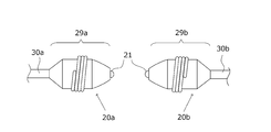
- FIG. 1A and 1B are schematic cross-sectional views of a discharge lamp.
- FIG. 1B is a schematic cross-sectional view enlarging the vicinity of the electrode tip of FIG. 1A.
- the discharge lamp 10 has a substantially spherical light emitting portion 11 formed by a discharge vessel made of quartz glass.
- the material of the discharge vessel is not limited to quartz glass, and may be made of other materials.
- a pair of electrodes 20a and 20b are disposed to face each other at an extremely small interval of, for example, 2 mm or less.
- sealing portions 12 are formed at both ends of the light emitting portion 11.
- a conductive metal foil 13 made of molybdenum or the like is hermetically embedded in the sealing portion 12 by, for example, a shrink seal.
- the shaft portions of the electrodes 20a and 20b are joined to one end of the metal foil 13, and the external lead 14 is joined to the other end of the metal foil 13, and power is supplied from a discharge lamp lighting device to be described later.
- Mercury is used to obtain the necessary visible light wavelength, for example, radiation having a wavelength of 360 to 780 nm, and, in terms of specific values, 0.20 mg / mm 3 or more is enclosed.
- a high vapor pressure of 200 atm or more is realized as the pressure inside the light emitting unit during lighting.
- argon gas is sealed at about 13 kPa. Its function is to improve the lighting startability.
- halogen gas iodine, bromine, chlorine, etc. are enclosed in the form of a compound with mercury or other metals.
- the amount of enclosed halogen is selected from the range of 10 ⁇ 6 ⁇ mol / mm 3 to 10 ⁇ 2 ⁇ mol / mm 3 .
- the biggest reason for enclosing the halogen is to extend the life of the discharge lamp using a so-called halogen cycle.
- the discharge lamp 10 is extremely small and has a very high lighting vapor pressure, the effect of preventing devitrification of the discharge vessel can be obtained by enclosing the halogen.
- Devitrification means that crystallization proceeds from a metastable glass state and changes to an aggregate of crystal grains grown from many crystal nuclei. If such a phenomenon occurs, light is scattered at the grain boundaries of the crystal and the discharge vessel becomes opaque.
- the gas enclosed with the light emission part 11 is not limited to the said gas.
- the maximum outer diameter of the light emitting part is 9.4 mm
- the distance between the electrodes is 1.0 mm
- the inner volume of the discharge vessel is 55 mm 3
- the rated voltage is 70 V
- the rated power is 180 W. It can be set as a structure.
- the discharge lamp 10 when it is assumed that a discharge lamp 10 is built in and used in a projector that has been miniaturized in recent years, the discharge lamp 10 is required to be extremely small as a whole size, and on the other hand, a high light emission amount is also required. . For this reason, the thermal influence in the light emitting portion is extremely severe, and the lamp wall load value of the lamp is 0.8 to 2.5 W / mm 2 , specifically 2.4 W / mm 2 . As described above, the discharge lamp 10 having a high mercury vapor pressure and a tube wall load value is mounted on a presentation device such as a projector or an overhead projector, thereby providing the presentation device with emitted light having good color rendering properties. be able to.
- a presentation device such as a projector or an overhead projector
- the electrode 20a includes a head portion 29a and a shaft portion 30a
- the electrode 20b includes a head portion 29b and a shaft portion 30b.
- Each of the electrode 20a and the electrode 20b has a protrusion 21 at the tip.
- the protrusion 21 is formed by agglomerating molten electrode material at the electrode tip when the lamp is turned on.
- the electrode 20a and the electrode 20b are described as both made of tungsten, but the material is not limited to this.
- the electrode 20a and the electrode 20b are energized, the electrode 20a is heated to a high temperature, and the tungsten constituting them is sublimated.
- the sublimated tungsten is combined with the enclosed halogen gas in the inner wall surface region of the light emitting portion 11 which is a relatively low temperature portion to form tungsten halide. Since the vapor pressure of tungsten halide is relatively high, it moves again in the vicinity of the tips of the electrodes 20a and 20b in the gas state. When heated again at this point, the tungsten halide is separated into halogen and tungsten.
- tungsten returns to the tips of the electrodes 20 a and 20 b and aggregates, and the halogen returns as the halogen gas in the light emitting unit 11. This corresponds to the “halogen cycle” described above.
- the agglomerated tungsten adheres to the vicinity of the tips of the electrode 20a and the electrode 20b, whereby the protrusion 21 is formed.
- FIG. 2 is a circuit block diagram schematically showing the configuration of the discharge lamp lighting device of the present invention.
- the lighting device 1 includes a power supply unit 3, a pulse generation unit 4, and a power control unit 5.
- the pulse generation unit 4 includes a frequency setting unit 41 and a pulse generation circuit 43, and a pulse P having a frequency set by the frequency setting unit 41 is generated by the pulse generation circuit 43 and supplied to the power supply unit 3.
- the power feeding unit 3 generates an alternating current based on a signal (corresponding to the gate signal Gx in FIG. 2) related to the control power value output from the power control unit 5 and the pulse P, and supplies the alternating current to the discharge lamp 10. .
- the discharge lamp 10 lights up when this alternating current is supplied.
- the power feeding unit 3 includes a step-down chopper unit 31, a DC / AC conversion unit 32, and a starter unit 33.
- the step-down chopper unit 31 steps down the supplied direct-current voltage Vdc to a desired direct-current voltage (hereinafter, referred to as “applied voltage” as appropriate), and outputs it to the subsequent DC / AC conversion unit 32.
- the step-down chopper unit 31 includes a switching element Qx, a reactor Lx, a diode Dx, a smoothing capacitor Cx, a resistor Rx, and a voltage dividing resistor (R1, R2). Yes.
- Switching element Qx has one end connected to the + side power supply terminal to which DC voltage Vdc is supplied and the other end connected to one end of reactor Lx.
- the diode Dx has a cathode terminal connected to a connection point between the switching element Qx and the reactor Lx, and an anode terminal connected to the negative side power supply terminal.
- the smoothing capacitor Cx has one end (+ side terminal) connected to the output side terminal of the reactor Lx and the other end ( ⁇ side terminal) connected to the output side terminal of the resistor Rx.
- the resistor Rx is connected between the negative terminal of the smoothing capacitor Cx and the anode terminal of the diode Dx, and realizes a current detection function.
- the voltage dividing resistors (R1, R2) are connected between the negative side terminal and the positive side terminal of the smoothing capacitor Cx to realize a voltage detection function.
- the switching element Qx is driven by a gate signal Gx output from the power control unit 5. Based on the duty of the gate signal Gx, the step-down chopper unit 31 steps down the DC voltage Vdc to a voltage corresponding to the duty and outputs the voltage to the subsequent DC / AC conversion unit 32. That is, the voltage applied to the discharge lamp 10 is determined by the signal from the power control unit 5.
- the DC / AC conversion unit 32 converts the input DC voltage into an AC voltage having a desired frequency and outputs the AC voltage to the subsequent starter unit 33.
- FIG. 2 shows a specific configuration example in which the DC / AC converter 32 is configured by switching elements Q1 to Q4 connected in a bridge shape (full bridge circuit).
- the switching element Q1 is driven by a gate signal G1 output from the driver 35.
- the switching element Q2 is driven by the gate signal G2
- the switching element Q3 is driven by the gate signal G3
- the switching element Q4 is driven by the gate signal G4.
- the driver 35 outputs a gate signal to alternately repeat on / off for the pair of switching elements Q1 and Q4 and the pair of switching elements Q2 and Q3 arranged diagonally. Thereby, a rectangular wave AC voltage is generated between the connection point of the switching elements Q1 and Q2 and the connection point of the switching elements Q3 and Q4.
- the starter unit 33 is a circuit unit for boosting the AC voltage supplied from the DC / AC conversion unit 32 when starting the discharge lamp and supplying the boosted voltage to the discharge lamp 10.
- the starter unit 33 is configured by a coil Lh and a capacitor Ch.
- an AC voltage having a high switching frequency for example, several hundred kHz
- a high switching frequency for example, several hundred kHz
- the frequency of the AC voltage supplied from the DC / AC converter 32 is shifted to a steady frequency (for example, 60 to 1000 Hz), and a steady lighting operation is performed.
- This steady frequency corresponds to the frequency of a pulse P1 described later.
- the change in the frequency of the AC voltage supplied to the starter unit 33 is performed by switching on / off the switching element Q1 and Q4 group and the switching element Q2 and Q3 group in the DC / AC conversion unit 32. This can be achieved by adjusting the period. Further, the change of the peak value of the AC voltage supplied to the starter unit 33 can be achieved by adjusting the operation duty of the switching element Qx in the step-down chopper unit 31.
- the switching element Qx of the step-down chopper unit 31 is turned on / off at a switching frequency corresponding to the duty of the gate signal Gx output from the power control unit 5, thereby changing the power supplied to the discharge lamp 10.
- the power control unit 5 performs control to increase the duty of the gate signal Gx so that a desired power value is obtained.
- the power control unit 5 includes a power calculation unit 51, a comparison unit 53, and a pulse width modulation circuit 55.
- Power calculating unit 51 voltage dividing resistors voltage signal detected by (R1, R2) V L, and a current signal I L that has been detected by the resistor Rx is input, generates a power signal W L based on these signals.
- Comparing unit 53 compares the power value as a reference, a power signal W L which is output from the power calculating unit 51, and outputs the comparison result to the pulse width modulation circuit 55.
- the pulse width modulation circuit 55 changes the duty ratio of the gate signal Gx according to the comparison result from the comparison unit 53.
- the voltage signal V L corresponds to a voltage generated by dividing the DC voltage (that is, the applied voltage) stepped down by the step-down chopper unit 31 by the voltage dividing resistors (R1, R2), and depends on the lamp voltage. Voltage.
- the current signal IL is also a current corresponding to the lamp current. Therefore, the power control unit 5 has a function of performing feedback control so that the applied power is constant, that is, power consumption in the discharge lamp 10 is constant.
- the pulse generation unit 4 includes the frequency setting unit 41 and the pulse generation circuit 43.
- the pulse generation circuit 43 generates a pulse P having a frequency set by the frequency setting unit 41 and outputs the pulse P to the driver 35 of the DC / AC conversion unit 32.
- switching control is performed on the switching elements Q1 to Q4 of the DC / AC conversion unit 32.
- the frequency setting unit 41 can be configured by, for example, a microcomputer.
- FIGS. 3A to 3C are diagrams showing examples of the waveform of the pulse P output from the pulse generator 4, that is, the lamp current waveform of the discharge lamp 10.
- FIG. 3A to 3C correspond to the waveforms of the pulses P in different time zones, respectively.
- the pulse P generated from the pulse generator 4 outputs a pulse P1 (corresponding to the “first pulse”) having a fundamental frequency f1 (pulse width W1) for a predetermined period T1, and then a frequency f2 (lower than the fundamental frequency f2).
- a cycle of outputting a pulse P2 (corresponding to “second pulse”) having a pulse width W2) for a predetermined period T2 is repeated.
- the frequency f2 of the second pulse P2 is different, that is, the pulse width W2 and the output period T2 are also different.
- the frequency setting unit 41 may employ a configuration including a memory that stores the number of continuous pulses of the first pulse P1, the number of continuous pulses of the second pulse P2, and the frequency f1 of the first pulse P1. Further, as will be described later, the frequency setting unit 41 sets the frequency f2 of the second pulse P2 according to the value of the applied voltage.
- the pulse generation circuit 43 includes a counter that counts the number of pulses P output from the pulse generation circuit 43, and information on this counter can be sent to the frequency setting unit 41.
- the frequency setting unit 41 switches the first pulse P1 to the second pulse P2 and the second pulse P2 to the second pulse P2 based on the information on the number of pulses given from the counter and the information stored in the memory.
- the timing of switching to one pulse P1 is recognized, and information on each frequency (f1, f2) can be output to the pulse generation circuit 43 in accordance with each timing.
- information on the pulse width W1 of the first pulse P1 and the pulse width W2 of the second pulse P2 may be used instead of the information on the frequency f1 of the first pulse P1 and the frequency f2 of the second pulse P2. I do not care.
- the frequency f1 (fundamental frequency) of the first pulse P1 corresponds to the fundamental frequency when the discharge lamp 10 is steadily lit and is, for example, one frequency selected from the range of 60 to 1000 Hz.
- the second pulse P2 is a low frequency inserted after a predetermined number of first pulses P1 are continuously output, and the frequency f2 is lower than the fundamental frequency, for example, from a range of 5 to 200 Hz. The selected frequency.
- the second pulse P2 is preferably inserted at a time interval of 0.01 seconds to 120 seconds.
- the pulse P2 is inserted at a time interval shorter than 0.01 seconds, the projection 21 serving as the starting point of the arc is excessively heated, and the shape thereof may be deformed or possibly disappear.
- the time interval is too wide, the state in which the minute protrusions are formed at the peripheral position of the protrusion 21 is maintained for a long time, and an arc starting from the minute protrusion may be formed during this time. is there.
- the period T2 during which the second pulse P2 is output is set to one period of the pulse P2. That is, in this period T2, the pulse generation circuit 43 is configured to output positive and negative pulses once each.
- the output form of the pulse P2 is not limited to such a form.
- the pulse generation circuit 43 outputs the first pulse P1 only for a predetermined period T1
- the second pulse P2 is output only for the half cycle length T2
- the first pulse P1 is output only for the time T1
- the second pulse P2 Alternatively, a configuration may be adopted in which the polarity is changed as before and only the half cycle length T2 is output.
- the second pulse P2 included in the pulse P output from the pulse generation circuit 43 may be included over a period of one cycle or more, such as 1.5 cycles of the second pulse P2.
- the electrode may be heated too much and the shape of the protrusion 21 serving as the arc starting point may change, so the second pulse P2 is applied for one cycle within one cycle. It is preferable to keep within.
- the frequency setting unit 41 sets the frequency f2 of the second pulse P2 according to the value of the applied voltage. Specifically, when the applied voltage matches a predetermined reference value, the frequency f2 of the second pulse P2 is set to a predetermined reference frequency. And when the value of an applied voltage exceeds this reference value, the frequency f2 of the 2nd pulse P2 is set to a frequency lower than a reference frequency. On the other hand, when the value of the applied voltage is lower than the reference value, the frequency f2 of the second pulse P2 is set to a frequency equal to or lower than the reference frequency.
- the frequency setting unit 41 is supplied with the voltage signal V L from the power supply unit 3 (see FIG. 2).
- the voltage signal V L corresponds to a voltage generated by dividing the DC voltage stepped down by the step-down chopper unit 31 by the voltage dividing resistors (R1, R2). According to the voltage. Therefore, the frequency setting unit 41 can detect the applied voltage based on the voltage signal VL .
- the frequency setting unit 41 may store the relationship between the applied voltage and the frequency f2 of the second pulse P2 in the form of a data table, or may store it in a predetermined relational expression.
- the frequency setting unit 41 uses the second pulse so that the frequency decreases as the value of the applied voltage increases from the reference value both when the applied voltage exceeds the reference value and when the applied voltage falls below the reference value.
- the frequency f2 of P2 is set will be described. In this case, when the applied voltage matches the reference value, the frequency f2 of the second pulse P2 indicates the highest frequency (corresponding to the “reference frequency”).
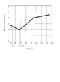
- FIG. 4 is an example of a graph showing the relationship between the applied voltage and the second pulse P2.
- the relationship between the applied voltage and the pulse width W2 of the second pulse P2 is shown.
- the example of FIG. 4 shows that when the applied voltage is 68 V, which is the reference value, the pulse width W2 of the second pulse P2 is the shortest and the frequency f2 at this time is the highest. Yes.
- the numerical values shown in FIG. 4 are merely examples.
- FIG. 3B corresponds to an example of the waveform of the pulse P when the applied voltage is 68V, for example.
- 3C corresponds to an example of the waveform of the pulse P when the applied voltage is 90 V, for example.
- FIG. 3A corresponds to an example of the waveform of the pulse P when the applied voltage is 55 V, for example.
- the pulse width W2 of the second pulse P2 is the shortest, and the frequency f2 of the second pulse P2 is the highest.
- the frequency f2 of the second pulse P2 shown in FIG. 3A is lower than the frequency f2 of the second pulse P2 shown in FIG. 3B.
- the frequency f2 of the second pulse P2 shown in FIG. 3C is lower than the frequency f2 of the second pulse P2 shown in FIG. 3A.
- the reference value is set to 68 V.
- the design of the electrodes (20a, 20b), the internal volume of the light emitting unit 11 (discharge vessel), the amount of enclosed mercury, and the like of the discharge lamp 10 itself is a value set as appropriate according to the design.
- Example 1 The case where the discharge lamp 10 was turned on by the discharge lamp lighting device 1 described above was taken as Example 1.
- the frequency of the first pulse P1 was 370 Hz (pulse width was about 1.4 ms).
- the specifications of the discharge lamp 10 are as follows.
- FIG. 5A is a graph showing the relationship between the applied voltage and the second pulse P2 in the case of Comparative Example 1 following FIG.
- Comparative Example 2 When the applied voltage is increased, the frequency f2 of the second pulse P2 is decreased (the pulse width W2 is increased), and when the applied voltage is decreased, the frequency f2 of the second pulse P2 is increased (the pulse width W2 is decreased).
- the case where the frequency f2 of the second pulse P2 was adjusted was referred to as Comparative Example 2.
- This comparative example 2 assumes the lighting method disclosed in Patent Document 2. The other points are common to the first embodiment.
- FIG. 5B is a graph showing the relationship between the applied voltage and the second pulse P2 in the case of Comparative Example 2 following FIG.
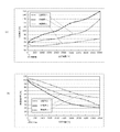
- FIG. 6 is a graph comparing changes over time in applied voltage and illuminance maintenance ratio when the discharge lamp is turned on in each lighting device in each of Example 1, Comparative Example 1, and Comparative Example 2.
- 6A is a graph showing the relationship between the applied voltage and the elapsed time
- FIG. 6B is a graph showing the relationship between the illuminance maintenance rate and the elapsed time.
- the “illuminance maintenance rate” is a value indicating the ratio of the brightness at each time point when the brightness immediately after lighting is set as a reference (100%).
- Comparative Example 1 is about 400 hours and Comparative Example 2 is about 2000 hours, whereas Example 1 is about 5000 hours.
- the applied voltage after 5000 hours from the start of lighting was 150 V in Comparative Example 1 and 130 V in Comparative Example 2, whereas Example 1 remained at 80 V.
- Comparative Example 1 has the fastest applied voltage increase rate, and Comparative Example 2 has a lower applied voltage increase rate than Comparative Example 1. This confirms the effect of reducing the frequency f2 of the second pulse P2 as the applied voltage increases.
- Comparative Example 1 is about 1500 hours and Comparative Example 2 is about 2300 hours, whereas Example 1 is About 3500 hours.
- the illuminance maintenance rate after 5000 hours from the start of lighting was about 23% in Comparative Example 1 and about 27% in Comparative Example 2, whereas it was 50% in Example 1.
- Comparative Example 1 has the fastest decrease rate of the illuminance maintenance rate
- Comparative Example 2 has a lower decrease rate than Comparative Example 1.
- the illumination maintenance rate tends to decrease as the distance between the electrodes becomes longer compared to the time of the initial lighting, and the comparison that can suppress the speed at which the distance between the electrodes becomes longer is suppressed. It can be seen that Example 2 can suppress the rate of decrease in the illuminance maintenance rate more than Comparative Example 1.
- Example 1 the increase in applied voltage and the decrease in the illuminance maintenance rate in Example 1 can be largely suppressed as compared with both Comparative Example 1 and Comparative Example 2. That is, according to the discharge lamp lighting device 1 described above, it is suggested that the life of the discharge lamp can be further extended, particularly compared with the method of Comparative Example 2.
- FIG. 6 (a) it can be seen that the applied voltage is lower in Example 1 than in Comparative Example 1 and Comparative Example 2 in the initial lighting stage until about 200 hours have elapsed since the start of lighting.
- FIG. 6B in this initial lighting stage, unlike Example 1 and Comparative Example 2, in Example 1, the illuminance maintenance rate is higher than immediately after lighting.
- the pulse width W2 of the second pulse P2 is increased to further reduce the frequency f2. In the initial stage of lighting, the electrode material is abundant.
- the distance between the electrodes can be shortened in the initial stage, and the time during which the discharge lamp 10 can be lit with a low applied voltage can be lengthened. Can be made longer. In addition, since the speed at which the distance between the electrodes becomes longer can be suppressed, the life of the discharge lamp can be extended as compared with the conventional case.
- the pulse width W2 of the second pulse P2 is the shortest when the applied voltage is the reference value (the frequency f2 is the highest), and the pulse width W2 becomes longer as the applied voltage falls below the reference value. This is explained assuming that the frequency f2 becomes lower (see FIG. 4). However, when the applied voltage is below the reference value, the pulse width W2 of the second pulse P2 may be equal to the pulse width W2 at the reference value.
- FIG. 7 is an example of a graph showing the relationship between the applied voltage and the second pulse P2 at this time.
- the discharge lamp 10 is assumed to be subjected to constant power control.
- eco mode a lighting method that switches the lighting power value itself, for example, when the projector apparatus is used with reduced brightness on the screen.
- normal mode a lighting method that switches the lighting power value itself
- the lighting power in normal time hereinafter referred to as “normal mode”
- the lighting power in the eco mode is 120 W.
- the frequency setting unit 41 is configured to receive a power signal W L from the power calculating unit 51, according to the value of the power signal W L, the frequency f2 of the second pulse P2 (pulse The width W2) may be changed.
- the pulse width W2 of the second pulse P2 may be used to set the ratio corresponding to the rate of change of the power signal W L.
- the pulse generation unit 4 has been described as repeating the cycle of outputting the first pulse P1 for a predetermined time and then outputting the second pulse P2 for a predetermined period.
- the pulse generator 4 outputs a lower-frequency third pulse instead of the second pulse P2, and then returns to the cycle in which the first pulse P1 and the second pulse P2 are output again. It doesn't matter.
- the third pulse is exceptionally output instead of the second pulse P2 only once every several tens to several hundreds of cycles for the purpose of eliminating the moved protrusion.
- SYMBOLS 1 Discharge lamp lighting device 3: Power supply part 4: Pulse generation part 5: Power control part 10: Discharge lamp 11: Light emission part 12: Sealing part 13: Metal foil 14: External lead 20a, 20b: Electrode 21: Protrusion 29a 29b: Electrode head 30a, 30b: Electrode shaft 31: Step-down chopper 32: DC / AC converter 33: Starter 35: Driver 41: Frequency setting unit 43: Pulse generation circuit 51: Power calculation unit 53 : Comparison unit 55: Pulse width modulation circuit
Abstract
従来の点灯方式で点灯する場合よりも放電ランプの長寿命化が図られる点灯方式を実現する。 放電ランプ点灯装置は、パルス発生部と、供給される直流電圧を直流の印加電圧に変圧し、当該印加電圧を前記パルスの周波数に応じた交流電流に変換し、当該交流電流を放電ランプに供給する給電部を備える。パルス発生部は、第一パルスと、第一パルスよりも低周波の第二パルスとを交互に出力し得る構成である。第二パルスの周波数は、印加電圧の値が所定の基準値に一致する場合には所定の基準周波数に設定され、印加電圧の値が前記基準値を上回る場合には、基準周波数よりも低い周波数に設定され、印加電圧の値が前記基準値を下回る場合には、基準周波数以下の周波数に設定される。
Description
本発明はプロジェクタ等の光源に好適に使用される放電ランプの点灯装置に関する。
プロジェクタ装置の光源には、高い水銀蒸気圧の放電ランプが用いられている。このような高圧水銀ランプは、水銀蒸気圧を高くすることで、可視波長域の光を高い出力で得ることができる。
放電ランプは、放電容器によって形成されたほぼ球形の発光部を有し、この発光部の中には、一対の電極が例えば2mm以下という極めて小さい間隔で対向して配置されている。
このような放電ランプを長期間同じ状態で点灯した場合、高温により微小な突起が複数形成されたり、電極の先端表面部に微小な凹凸が発生したりすることがある。これらの微小突起や凹凸は、電極を構成する材料(例えばタングステン)が溶融し、発光部内に封入されたガスと結合して生じた化合物が凝集して生じたものであり、この存在が電極先端の表面部の形状を変化させる。これに伴ってアークの起点が移動し、放電位置が不安定となり、いわゆるフリッカと呼ばれる投射光のちらつきが発生することが問題となっていた。
このような問題を解決するため、下記特許文献1には、所定の周波数(基本周波数)の電流パルスP1を放電ランプに供給すると共に、基本周波数よりも低周波の電流パルスP2を電流パルスP1に間欠的又は周期的に挿入する放電ランプの点灯方式が開示されている(図9参照)。
電流パルスの周波数を低周波とすることで、一方の電極が陽極に、他方の電極が陰極に固定化される期間、つまり両電極間に高電圧が印加される期間が長くなる。この結果、電極に対する加熱の度合いが高まり、電極先端のみならず先端から離れた箇所に対しても熱を伝達させることができる。よって、低周波の電流パルスが印加される間、電極先端から離れた箇所に対しても熱が伝達され、かかる箇所に生じていた微小突起や凹凸を溶融、蒸発させることができる。これにより、悪影響を及ぼし兼ねない電極先端部以外の突起や凹凸を消滅させることができ、アークの輝点を安定化させることができる。
ところで、放電ランプは、給電部(給電装置)によって定電力点灯制御が行われるのが一般的である。この制御は、放電ランプからの光出力を安定に保つ目的と、放電ランプへの負荷、より詳細には、石英ガラス等で構成される放電容器への熱的負荷を一定に保つ目的のために行われる。
放電ランプは、点灯時間の経過と共に電極が消耗し、電極間距離が長くなる。電極間距離が長くなると、放電ランプへの印加電圧(ランプ電圧)が上昇する。このため、定電力点灯制御下では、放電ランプへの印加電流(ランプ電流)が低下する。ランプ電流が低下すると、電極への熱の流入が減少する。よって、この状態では、低周波のパルスP2を放電ランプに供給しても、電極に流入される熱量が減少し、上述した電極先端部以外の突起や凹凸を消滅させる効果が低下してしまう。
この点を鑑み、下記特許文献2には、ランプ電圧の変化を検出し、ランプ電圧が上昇した場合、すなわちランプ電流が低下した場合には、低周波の電流パルスの周波数を更に低下させる(パルス幅を長くする)制御を行う放電ランプの点灯方式が開示されている。
近年、更に点灯時間の長い放電ランプが要求されている。本発明は、上述した従来の点灯方式で点灯する場合よりも放電ランプの長寿命化が図られる点灯方式を実現することを目的とする。
本発明者は、鋭意研究により、低い印加電圧の下で点灯させると寿命特性が良好になることを見出した。本発明は、この新しい知見の下になされたものである。
本発明は、所定のガスが封入された放電容器内に一対の電極が対向配置された放電ランプに対して交流電流を供給する放電ランプ点灯装置であって、
パルスを発生するパルス発生部と、
供給される直流電圧を直流の印加電圧に変圧し、当該印加電圧を前記パルスの周波数に応じた交流電流に変換し、当該交流電流を前記放電ランプに供給する給電部とを備え、
前記パルス発生部は、
第一パルスと、前記第一パルスよりも低周波の第二パルスとを交互に出力し得る構成であり、
前記印加電圧の値が所定の基準値に一致する場合には、前記第二パルスの周波数を所定の基準周波数に設定し、
前記印加電圧の値が前記基準値を上回る場合には、前記第二パルスの周波数を前記基準周波数よりも低い周波数に設定し、
前記印加電圧の値が前記基準値を下回る場合には、前記第二パルスの周波数を前記基準周波数以下の周波数に設定することを特徴とする。
特許文献2に記載の点灯方式では、印加電圧が上昇すると低周波の電流パルスの周波数を低下させる一方、印加電圧が低下すると低周波のパルスの周波数を上昇させていた。
低周波の電流パルスの周波数を低下させることで、一対の電極間に印加される電圧の極性を一定に維持する(極性反転しない)時間を長くして電極に供給される熱量を増加させ、電極温度を高めて余分な突起や凹凸を溶融、蒸発させることができる。蒸発した電極材料は、その後に電極先端に凝集されることで、電極間距離が短くなる方向にシフトする。この結果、印加電圧が低下する方向に動く。電極材料の蒸発量と凝集量がバランスされていると、印加電圧を一定に保つことができる。ただし、点灯時間が長くなるに連れ、電極材料が放電容器に付着する等して蒸発量が凝集量を上回るため、電極間距離はどうしても伸びてしまい、印加電圧の上昇は避けられない。
逆の理由により、低周波の電流パルスの周波数を上昇させると、電極に供給される熱量が低下するため、電極材料の蒸発量は低下する。このため、その後の電極材料の凝集量も低下し、電極間距離は長くなる方向にシフトする。この結果、印加電圧が上昇する方向に動く。
つまり、特許文献2に記載の点灯方法は、印加電圧、すなわち電極間距離をなるべく一定にすることを意図したものであるといえる。しかし、実際には点灯時間が長くなるに連れ印加電圧が上昇することは既に述べた通りである。
これに対し、本発明の方法は、印加電圧が高い場合、すなわち印加電圧の値が所定の基準値を上回る場合において、低周波のパルス(第二パルス)の周波数を低くする一方、印加電圧が低い場合、すなわち印加電圧の値が前記基準値を下回る場合には、第二パルスの周波数を基準周波数以下の周波数に設定している。
ここで、印加電圧が高い場合に第二パルスの周波数を低くする意図は、特許文献2に記載の点灯方式と同じである。一方、印加電圧が低い場合、特許文献2に記載の点灯方式では第二パルスの周波数を高く設定していたのに対し、本発明の構成では、第二パルスの周波数を基準周波数以下の周波数に設定している。上述したように、印加電圧が基準値である場合の第二パルスの周波数を基準周波数に設定することに鑑みれば、印加電圧が基準値を下回る場合に、第二パルスの周波数を基準周波数以下に設定するという本発明の構成は、特許文献2に記載の点灯方式とは大きく異なっている。この構成は、印加電圧(ランプ電圧)が低い状態においては、意図的に印加電圧を更に下げる方向に第二パルスの周波数を制御することを目的としている。
上述したように、放電ランプは、点灯時間の経過と共に電極が消耗し、電極間距離が長くなり、印加電圧が上昇する。他方、点灯の初期段階においては、電極先端形状は摩耗しておらず、突起を生成するのに必要な電極材料が潤沢に存在している。このため、初期時においては低い印加電圧で放電ランプの点灯が可能である。
ここで、電極材料が潤沢に存在している初期段階において、低周波のパルス(第二パルス)の周波数を低下させると、電極に供給される熱量が増加して、蒸発する電極材料の量は多くなる。このため、その後に凝集される電極材料の量も多くなり、電極間距離が短くなる。この結果、印加電圧は更に低下する。
すなわち、このような制御を採用することで、低い印加電圧で放電ランプを点灯することができる期間が長くなる。この結果、従来の点灯方式で点灯するよりも放電ランプを長時間にわたって点灯させることができる。
また、上記構成に加えて、前記パルス発生部は、前記印加電圧の値が前記基準値を下回る場合において、前記印加電圧の値が前記基準値から離れるほど前記第二パルスの周波数を低下させるものとしても構わない。
このような構成とすることで、低い印加電圧で放電ランプの点灯が可能な場合において、更に低い印加電圧で点灯させることができる。これにより、放電ランプの長寿命化を更に高めることができる。
なお、前記パルス発生部は、周波数を設定する周波数設定部と、前記周波数設定部によって設定された周波数のパルスを生成して出力するパルス発生回路を備える構成とすることができる。このとき、周波数設定部が、印加電圧の値に応じて第二パルスの周波数を設定する構成とすることができる。
より詳細には、前記放電ランプ点灯装置は、上記の構成に加えて、
前記印加電圧及び印加電力を検出すると共に、検出された前記印加電力を所定の電力値に維持させるように、前記直流電圧から前記印加電圧に変圧するときの変圧比を制御する電力制御部とを備え、
前記パルス発生部は、周波数を設定する周波数設定部と、前記周波数設定部によって設定された周波数の前記パルスを生成して出力するパルス発生回路とを備え、
前記周波数設定部は、前記電力検出部からの信号に基づいて検知した前記印加電圧の値に応じて前記第二パルスの周波数を設定する構成とすることができる。
前記印加電圧及び印加電力を検出すると共に、検出された前記印加電力を所定の電力値に維持させるように、前記直流電圧から前記印加電圧に変圧するときの変圧比を制御する電力制御部とを備え、
前記パルス発生部は、周波数を設定する周波数設定部と、前記周波数設定部によって設定された周波数の前記パルスを生成して出力するパルス発生回路とを備え、
前記周波数設定部は、前記電力検出部からの信号に基づいて検知した前記印加電圧の値に応じて前記第二パルスの周波数を設定する構成とすることができる。
本発明の放電ランプ点灯装置によれば、従来よりも放電ランプの点灯時間を長くすることができ、放電ランプの長寿命化が実現される。
本発明の放電ランプ点灯装置の実施形態につき、図面を参照して説明する。ここで、点灯装置の構成に関する説明に先立ち、当該点灯装置によって交流電流が供給される対象となる放電ランプの構成の一例について、図面を参照して説明する。なお、各図において図面の寸法比と実際の寸法比は必ずしも一致しない。
[ランプの構成]
図1A及び図1Bに、放電ランプの断面模式図を示す。図1Bは、図1Aの電極先端付近を拡大した断面模式図である。
図1A及び図1Bに、放電ランプの断面模式図を示す。図1Bは、図1Aの電極先端付近を拡大した断面模式図である。
放電ランプ10は、石英ガラスからなる放電容器によって形成された、ほぼ球形の発光部11を有する。放電容器の材料は石英ガラスに限定されず、他の材料で構成されていても構わない。
この発光部11の中には、一対の電極20a、20bが例えば2mm以下という極めて小さい間隔で対向配置している。
また、発光部11の両端部には封止部12が形成される。この封止部12には、モリブデン等で構成された導電用の金属箔13が、例えばシュリンクシールにより気密に埋設されている。金属箔13の一端には電極20a、20bの軸部が接合しており、金属箔13の他端には外部リード14が接合し、後述する放電ランプ点灯装置から電力が供給される。
放電ランプ10の発光部11には、水銀、希ガス、及びハロゲンガスが封入されている。
水銀は、必要な可視光波長、例えば、波長360~780nmの放射光を得るためのものであり、具体的数値でいうと、0.20mg/mm3以上封入されている。この封入量は温度条件によっても異なるが、点灯時における発光部内部の圧力を200気圧以上という高い蒸気圧を実現するものである。また、水銀をより多く封入することで点灯時の水銀蒸気圧250気圧以上、300気圧以上という高い水銀蒸気圧の放電ランプを作ることができ、水銀蒸気圧が高くなるほどプロジェクタに適した光源を実現できる。
希ガスとしては、例えばアルゴンガスが約13kPa封入される。その機能は点灯始動性を改善することにある。
また、ハロゲンガスとしては、ヨウ素、臭素、塩素などが水銀又はその他の金属との化合物形態で封入される。ハロゲンの封入量は、10-6μmol/mm3~10-2μmol/mm3の範囲から選択される。ハロゲンを封入する最大の理由は、いわゆるハロゲンサイクルを利用した放電ランプの長寿命化のためである。また、放電ランプ10を極めて小型で且つ極めて高い点灯蒸気圧とした場合には、ハロゲンを封入することで放電容器の失透防止という作用も得られる。失透とは、準安定のガラス状態から結晶化が進行し、多くの結晶核から成長した結晶粒の集合体へと変化することをいう。仮にこのような現象が生じると、結晶の粒界で光が散乱されて放電容器が不透明になってしまう。
なお、同様の機能を実現できるのであれば、発光部11に封入されるガスは上記ガスに限定されるものではない。
放電ランプ10の一実施例としては、発光部の最大外径9.4mm、電極間距離1.0mm、放電容器内容積55mm3、定格電圧70V、定格電力180Wであり交流方式で電力が供給される構成とすることができる。
また、近年において小型化が進行するプロジェクタに放電ランプ10を内蔵して利用することを想定した場合、放電ランプ10は全体寸法として極めて小型化が要請され、その一方で高い発光光量も要求される。このため、発光部内の熱的影響は極めて厳しいものとなり、ランプの管壁負荷値は0.8~2.5W/mm2、具体的には2.4W/mm2となる。このように、高い水銀蒸気圧や管壁負荷値を有する放電ランプ10が、プロジェクタやオーバーヘッドプロジェクタのようなプレゼンテーション用機器に搭載されることで、プレゼンテーション用機器に演色性の良い放射光を提供することができる。
[電極先端の形状]
図1Bに示すように、電極20aは頭部29aと軸部30aによって構成され、電極20bは頭部29bと軸部30bによって構成される。そして、電極20a及び電極20bには、いずれも先端に突起21が形成されている。この突起21は、ランプ点灯時、電極先端において溶融した電極材料が凝集して形成されるものである。本実施形態では、電極20a及び電極20bがいずれもタングステンで構成されるものとして説明するが、材料はこれに限定されるものではない。
図1Bに示すように、電極20aは頭部29aと軸部30aによって構成され、電極20bは頭部29bと軸部30bによって構成される。そして、電極20a及び電極20bには、いずれも先端に突起21が形成されている。この突起21は、ランプ点灯時、電極先端において溶融した電極材料が凝集して形成されるものである。本実施形態では、電極20a及び電極20bがいずれもタングステンで構成されるものとして説明するが、材料はこれに限定されるものではない。
電極20a及び電極20bに対して通電がされると、白熱して高温化され、これらを構成するタングステンが昇華する。昇華したタングステンは、比較的に低温部である発光部11の内壁面領域において、封入されていたハロゲンガスと結合して、ハロゲン化タングステンを形成する。ハロゲン化タングステンの蒸気圧は比較的高いことから、ガスの状態で再び電極20a及び電極20bの先端付近に再び移動する。そして、この箇所で再度加熱されると、ハロゲン化タングステンはハロゲンとタングステンに分離される。このうちタングステンは、電極20a及び電極20bの先端に戻って凝集され、ハロゲンは発光部11内のハロゲンガスとして復帰する。これが上記の「ハロゲンサイクル」に対応する。なお、この凝集されたタングステンが、電極20a及び電極20bの先端近傍に付着することで、突起21が形成される。
[点灯装置の構成]
図2は、本発明の放電ランプ点灯装置の構成を模式的に示す回路ブロック図である。図2に示すように、点灯装置1は、給電部3、パルス発生部4、及び電力制御部5を含んで構成される。パルス発生部4は、周波数設定部41及びパルス発生回路43を備えており、周波数設定部41によって設定された周波数のパルスPがパルス発生回路43において生成され、給電部3に供給される。給電部3は、電力制御部5から出力される制御電力値に関する信号(図2内におけるゲート信号Gxに対応する)と、パルスPとに基づいて交流電流を生成し、放電ランプ10に供給する。放電ランプ10は、この交流電流が供給されることで点灯する。
図2は、本発明の放電ランプ点灯装置の構成を模式的に示す回路ブロック図である。図2に示すように、点灯装置1は、給電部3、パルス発生部4、及び電力制御部5を含んで構成される。パルス発生部4は、周波数設定部41及びパルス発生回路43を備えており、周波数設定部41によって設定された周波数のパルスPがパルス発生回路43において生成され、給電部3に供給される。給電部3は、電力制御部5から出力される制御電力値に関する信号(図2内におけるゲート信号Gxに対応する)と、パルスPとに基づいて交流電流を生成し、放電ランプ10に供給する。放電ランプ10は、この交流電流が供給されることで点灯する。
〈給電部3〉
給電部3は、降圧チョッパ部31、DC/AC変換部32、及びスタータ部33を備える。
給電部3は、降圧チョッパ部31、DC/AC変換部32、及びスタータ部33を備える。
降圧チョッパ部31は、供給される直流電圧Vdcを所望電圧の直流電圧(以下、適宜「印加電圧」という。)に降圧し、後段のDC/AC変換部32に出力する。図2では、具体的な構成例として、降圧チョッパ部31は、スイッチング素子Qx、リアクトルLx、ダイオードDx、平滑コンデンサCx、抵抗Rx、及び分圧抵抗(R1,R2)を有するものが図示されている。
スイッチング素子Qxは、直流電圧Vdcが供給される+側電源端子に一端が接続され、他端がリアクトルLxの一端に接続される。ダイオードDxは、カソード端子がスイッチング素子Qx及びリアクトルLxの接続点に接続され、アノード端子が-側電源端子に接続される。平滑コンデンサCxは、一端(+側端子)がリアクトルLxの出力側端子に接続され、他端(-側端子)が抵抗Rxの出力側端子に接続される。抵抗Rxは、平滑コンデンサCxの-側端子とダイオードDxのアノード端子の間に接続され、電流検出の機能を実現している。また、分圧抵抗(R1,R2)は、平滑コンデンサCxの-側端子と+側端子の間に接続され、電圧検出の機能を実現している。
スイッチング素子Qxは、電力制御部5が出力するゲート信号Gxによって駆動される。このゲート信号Gxのデューティにより、降圧チョッパ部31は直流電圧Vdcをこのデューティに応じた電圧に降圧して後段のDC/AC変換部32に出力する。つまり、電力制御部5からの信号によって放電ランプ10への印加電圧が決定される。
DC/AC変換部32は、入力された直流電圧を所望の周波数の交流電圧に変換して、後段のスタータ部33に出力する。図2では、具体的な構成例として、DC/AC変換部32が、ブリッジ状に接続したスイッチング素子Q1~Q4から構成されたものが図示されている(フルブリッジ回路)。
スイッチング素子Q1は、ドライバ35から出力されるゲート信号G1によって駆動される。同様に、スイッチング素子Q2はゲート信号G2によって駆動され、スイッチング素子Q3はゲート信号G3によって駆動され、スイッチング素子Q4はゲート信号G4によって駆動される。ドライバ35は、対角に配置されたスイッチング素子Q1及びQ4の組と、スイッチング素子Q2及びQ3の組に対して、交互にオン/オフを繰り返すようにゲート信号を出力する。これにより、スイッチング素子Q1及びQ2の接続点と、スイッチング素子Q3及びQ4の接続点の間に、矩形波状の交流電圧が発生する。
スタータ部33は、放電ランプ始動時にDC/AC変換部32から供給される交流電圧を昇圧して放電ランプ10に供給するための回路部である。図2では、具体的な構成例として、スタータ部33が、コイルLh及びコンデンサChで構成されたものが図示されている。放電ランプ始動時に、コイルLh、コンデンサChからなるLC直列回路の共振周波数近傍の、高いスイッチング周波数(例えば数百kHz)の交流電圧をDC/AC変換部32から印加することで、スタータ部33の二次側において放電ランプの始動に必要な高い電圧が生成され、これが放電ランプ10に供給される。なお、放電ランプが点灯した後はDC/AC変換部32から供給される交流電圧の周波数を定常周波数(例えば60~1000Hz)に移行し、定常点灯動作が行われる。この定常周波数は、後述するパルスP1の周波数に対応する。
なお、上記回路において、スタータ部33に供給される交流電圧の周波数の変更は、DC/AC変換部32におけるスイッチング素子Q1及びQ4の組と、スイッチング素子Q2及びQ3の組のオン/オフ切替の周期を調整することで達成できる。また、スタータ部33に供給される交流電圧の波高値の変更は、降圧チョッパ部31におけるスイッチング素子Qxの動作デューティを調整することで達成できる。
すなわち、降圧チョッパ部31のスイッチング素子Qxは、電力制御部5が出力するゲート信号Gxのデューティに応じたスイッチング周波数でオン/オフし、これによって放電ランプ10に供給される電力が変化する。例えば放電ランプ10への供給電力を上昇させたい場合、電力制御部5は、所望の電力値となるようにゲート信号Gxのデューティを上げる制御を行う。
〈電力制御部5〉
本実施形態では、電力制御部5は、電力演算部51、比較部53、及びパルス幅変調回路55を備えている。
本実施形態では、電力制御部5は、電力演算部51、比較部53、及びパルス幅変調回路55を備えている。
電力演算部51は、分圧抵抗(R1,R2)によって検出した電圧信号VL、及び抵抗Rxによって検出した電流信号ILが入力され、これらの信号に基づいて電力信号WLを生成する。比較部53は、基準となる電力値と、電力演算部51から出力された電力信号WLとを比較し、比較結果をパルス幅変調回路55に出力する。パルス幅変調回路55は、比較部53からの比較結果に応じてゲート信号Gxのデューティ比を変更する。
電圧信号VLは、降圧チョッパ部31で降圧された直流電圧(すなわち印加電圧)が分圧抵抗(R1,R2)で分圧されて生成された電圧に対応するものであり、ランプ電圧に応じた電圧である。また、電流信号ILについても、ランプ電流に対応する電流である。よって、電力制御部5は、印加電力が一定になるように、すなわち放電ランプ10における消費電力が一定になるようにフィードバック制御する機能を有している。
〈パルス発生部4〉
上述したように、パルス発生部4は、周波数設定部41及びパルス発生回路43を備えている。パルス発生回路43は、周波数設定部41で設定された周波数のパルスPを生成し、DC/AC変換部32のドライバ35に出力する。前述したように、このパルスPに基づいて、DC/AC変換部32のスイッチング素子Q1~Q4に対するスイッチング制御が行われる。周波数設定部41は、例えばマイコン等によって構成されることができる。
上述したように、パルス発生部4は、周波数設定部41及びパルス発生回路43を備えている。パルス発生回路43は、周波数設定部41で設定された周波数のパルスPを生成し、DC/AC変換部32のドライバ35に出力する。前述したように、このパルスPに基づいて、DC/AC変換部32のスイッチング素子Q1~Q4に対するスイッチング制御が行われる。周波数設定部41は、例えばマイコン等によって構成されることができる。
パルス発生部4から出力されるパルスPにつき、図3A~図3Cを参照して説明する。図3A~図3Cは、パルス発生部4から出力されるパルスPの波形、すなわち放電ランプ10のランプ電流波形の一例を示す図である。なお、図3A~図3Cは、それぞれ異なる時間帯におけるパルスPの波形に対応している。
パルス発生部4から発生されるパルスPは、基本周波数f1(パルス幅W1)のパルスP1(「第一パルス」に対応)を所定期間T1の間出力した後、基本周波数よりも低い周波数f2(パルス幅W2)のパルスP2(「第二パルス」に対応)を所定期間T2の間出力するというサイクルを繰り返す。この点については、図9を参照して上述した内容と共通である。図3A、図3B、及び図3Cでは、それぞれ第二パルスP2の周波数f2が異なっており、すなわちパルス幅W2及び出力期間T2も異なっている。
例えば、周波数設定部41は、第一パルスP1の連続パルス数、第二パルスP2の連続パルス数、第一パルスP1の周波数f1を記憶したメモリを備える構成を採用することができる。また、後述するように、第二パルスP2の周波数f2については、周波数設定部41が印加電圧の値に応じて設定する。
更に、パルス発生回路43が、当該パルス発生回路43から出力されたパルスPのパルス数をカウントするカウンタを備えており、このカウンタの情報が周波数設定部41に送られる構成とすることができる。このとき、周波数設定部41は、カウンタから与えられるパルス数に関する情報と、メモリに記憶されている情報に基づいて、第一パルスP1から第二パルスP2に切り替えるタイミング、及び第二パルスP2から第一パルスP1に切り替えるタイミングを認識し、各タイミングに合わせて、それぞれの周波数(f1,f2)の情報をパルス発生回路43に出力することができる。
なお、上記において、第一パルスP1の周波数f1、第二パルスP2の周波数f2の情報に代えて、第一パルスP1のパルス幅W1、及び第二パルスP2のパルス幅W2の情報を用いても構わない。
第一パルスP1の周波数f1(基本周波数)とは、放電ランプ10を定常的に点灯する際の基本周波数に相当し、例えば60~1000Hzの範囲から選択された一の周波数である。また、第二パルスP2は、第一パルスP1が所定数連続的に出力された後に挿入される低周波であり、その周波数f2は、基本周波数よりも低周波の、例えば5~200Hzの範囲から選択された周波数である。
第二パルスP2は、0.01秒以上120秒以下の時間間隔で挿入されるのが好適である。言い換えれば、期間T1を0.01秒以上120秒以下の範囲に設定するのが好適であり、期間T1を0.01秒以上2秒以下の範囲に設定するのがより好適である。パルスP2を0.01秒より短い時間間隔で挿入すると、アークの起点となる突起21が加熱され過ぎてしまい、その形状が変形したり場合によっては消滅したりするおそれがあるためである。逆に、時間間隔をあまりに広くすると、突起21の周辺位置に微小突起が形成されたままの状態が長く維持されてしまい、この間に微小突起を起点とするアークが形成されるおそれがあるためである。
なお、図3A~図3Cの例では、第二パルスP2が出力される期間T2は、当該パルスP2の1周期の期間に設定されている。つまり、この期間T2内において、パルス発生回路43は、正極性と負極性のパルスを1回ずつ出力する構成である。しかし、パルスP2の出力態様は、このような形態に限られるものではない。
例えば、パルス発生回路43が所定期間T1だけ第一パルスP1を出力した後、第二パルスP2を半周期長T2だけ出力し、更に時間T1だけ第一パルスP1を出力した後、第二パルスP2を先ほどと極性を変えて半周期長T2だけ出力するという構成を採用しても構わない。更には、パルス発生回路43から出力されるパルスPに含まれる第二パルスP2を、当該第二パルスP2の1.5周期など、1周期以上の時間にわたって含ませる構成としても構わない。ただし、第二パルスP2の印加時間を伸ばし過ぎると、電極が加熱され過ぎてアーク起点となる突起21の形状が変化してしまうおそれがあるので、1サイクル内には第二パルスP2を1周期以内に留めるのが好適である。
そして、上述したように、本実施形態の放電ランプ点灯装置1において、周波数設定部41は、印加電圧の値に応じて第二パルスP2の周波数f2を設定する。具体的には、印加電圧が所定の基準値に一致する場合、第二パルスP2の周波数f2を所定の基準周波数に設定する。そして、印加電圧の値がこの基準値を上回る場合には、第二パルスP2の周波数f2を基準周波数よりも低い周波数に設定する。一方、印加電圧の値がこの基準値を下回る場合には、第二パルスP2の周波数f2を基準周波数以下の周波数に設定する。
放電ランプ点灯装置1において、周波数設定部41は給電部3から電圧信号VLが与えられる(図2参照)。上述したように、この電圧信号VLは、降圧チョッパ部31で降圧された直流電圧が分圧抵抗(R1,R2)で分圧されて生成された電圧に対応するものであり、印加電圧に応じた電圧である。よって、周波数設定部41は、電圧信号VLに基づいて印加電圧を検知することができる。周波数設定部41は、印加電圧と第二パルスP2の周波数f2の関係をデータテーブルの形式で記憶しているものとしても構わないし、所定の関係式で記憶しているものとしても構わない。
一例として、印加電圧が基準値を上回る場合、及び印加電圧が基準値を下回る場合の双方において、印加電圧の値が基準値から離れるほど周波数が低くなるように、周波数設定部41が第二パルスP2の周波数f2を設定する場合について説明する。この場合、印加電圧が基準値に一致しているときに第二パルスP2の周波数f2は最も高い周波数(上記「基準周波数」に対応)を示す。
図4は、印加電圧と第二パルスP2の関係を示すグラフの一例であり、ここでは印加電圧と第二パルスP2のパルス幅W2との関係を示している。図4の例では、印加電圧が基準値である68Vである場合に、第二パルスP2のパルス幅W2が最も短くなっており、このときの周波数f2が最も高くなっていることが示されている。なお、図4に示されている数値はあくまで一例である。
印加電圧と第二パルスP2の関係が、図4に示される関係下にある場合において、図3Bは、例えば印加電圧が68Vである場合のパルスPの波形の例に対応する。また、図3Cは、例えば印加電圧が90Vである場合のパルスPの波形の例に対応し、図3Aは、例えば印加電圧が55Vである場合のパルスPの波形の例に対応する。
図3A~図3Cの中では、図3Bにおいて、第二パルスP2のパルス幅W2が最も短くなっており、第二パルスP2の周波数f2が最も高い。図3Aに示される第二パルスP2の周波数f2は、図3Bに示される第二パルスP2の周波数f2よりも低い。図3Cに示される第二パルスP2の周波数f2は、図3Aに示される第二パルスP2の周波数f2よりも低い。
なお、ここでは、基準値を68Vとしているが、この基準値については、電極(20a,20b)の設計、発光部11(放電容器)の内容積、及び封入水銀量等、放電ランプ10自体の設計に応じて適宜設定される値である。
[作用]
以下において、上述した放電ランプ点灯装置1によって放電ランプ10を点灯した場合、従来の点灯装置によって点灯した場合よりも寿命が伸びることにつき、実施例を参照して説明する。
以下において、上述した放電ランプ点灯装置1によって放電ランプ10を点灯した場合、従来の点灯装置によって点灯した場合よりも寿命が伸びることにつき、実施例を参照して説明する。
(実施例1)
上述した放電ランプ点灯装置1によって放電ランプ10を点灯した場合を実施例1とした。なお、第一パルスP1の周波数を370Hz(パルス幅は約1.4ms)とした。また、放電ランプ10の仕様は以下の通りである。
上述した放電ランプ点灯装置1によって放電ランプ10を点灯した場合を実施例1とした。なお、第一パルスP1の周波数を370Hz(パルス幅は約1.4ms)とした。また、放電ランプ10の仕様は以下の通りである。
<放電ランプ10の仕様>
・定格電力:450W
・定格電圧:85V
・発光部の内容積:250mm3
・点灯開始前の電極間距離:1.5mm
・封入物:水銀0.29mg/mm3、アルゴンガス13kPa、ハロゲンガス10-6~10-2μmol/mm3
・定格電力:450W
・定格電圧:85V
・発光部の内容積:250mm3
・点灯開始前の電極間距離:1.5mm
・封入物:水銀0.29mg/mm3、アルゴンガス13kPa、ハロゲンガス10-6~10-2μmol/mm3
(比較例1)
第二パルスP2の周波数f2を印加電圧の値には関係なく、すなわちランプ電圧の値には関係なく一定値とした場合を比較例1とした。なお、他の点については実施例1と共通である。図5Aは、図4にならって、比較例1の場合における、印加電圧と第二パルスP2の関係を示したグラフである。
第二パルスP2の周波数f2を印加電圧の値には関係なく、すなわちランプ電圧の値には関係なく一定値とした場合を比較例1とした。なお、他の点については実施例1と共通である。図5Aは、図4にならって、比較例1の場合における、印加電圧と第二パルスP2の関係を示したグラフである。
(比較例2)
印加電圧が上昇すると第二パルスP2の周波数f2を低下させ(パルス幅W2を上昇させ)、印加電圧が低下すると第二パルスP2の周波数f2を上昇させる(パルス幅W2を低下させる)ように、第二パルスP2の周波数f2を調整した場合を比較例2とした。この比較例2は、特許文献2に開示されている点灯方法を想定したものである。なお、他の点については実施例1と共通である。図5Bは、図4にならって、比較例2の場合における、印加電圧と第二パルスP2の関係を示したグラフである。
印加電圧が上昇すると第二パルスP2の周波数f2を低下させ(パルス幅W2を上昇させ)、印加電圧が低下すると第二パルスP2の周波数f2を上昇させる(パルス幅W2を低下させる)ように、第二パルスP2の周波数f2を調整した場合を比較例2とした。この比較例2は、特許文献2に開示されている点灯方法を想定したものである。なお、他の点については実施例1と共通である。図5Bは、図4にならって、比較例2の場合における、印加電圧と第二パルスP2の関係を示したグラフである。
(結果分析)
図6は、実施例1、比較例1、比較例2のそれぞれにおいて、各点灯装置で放電ランプを点灯させたときの印加電圧及び照度維持率の経時的な変化を比較したグラフである。図6において、(a)が印加電圧と経過時間の関係を示すグラフであり、(b)が照度維持率と経過時間の関係を示すグラフである。なお、ここで「照度維持率」とは、点灯直後の明るさを基準(100%)としたときの、各時点における明るさの比率を示す値である。
図6は、実施例1、比較例1、比較例2のそれぞれにおいて、各点灯装置で放電ランプを点灯させたときの印加電圧及び照度維持率の経時的な変化を比較したグラフである。図6において、(a)が印加電圧と経過時間の関係を示すグラフであり、(b)が照度維持率と経過時間の関係を示すグラフである。なお、ここで「照度維持率」とは、点灯直後の明るさを基準(100%)としたときの、各時点における明るさの比率を示す値である。
図6(a)によれば、印加電圧が80Vに達するのに要した時間を比較すると、比較例1は約400時間、比較例2は約2000時間であるのに対し、実施例1は約5000時間である。点灯開始から5000時間後の印加電圧は、比較例1が150V、比較例2が130Vであるのに対し、実施例1は80Vに留まっていた。
比較例1は印加電圧の上昇速度が最も速く、比較例2は比較例1よりは印加電圧の上昇速度が抑制されている。これにより、印加電圧の上昇に伴って第二パルスP2の周波数f2を低下させたことの効果が確認される。
印加電圧が上昇することで放電ランプ10に供給される電流(ランプ電流)は低下するため、印加する電流の極性を反転させない(一方の極性を維持している)時間が一定である場合には、電極に供給される熱量は低下してしまう。この場合には電極先端部以外の突起や凹凸を消滅させる効果が低下してしまう。比較例2の場合、印加電圧の上昇に伴って第二パルスP2の周波数f2を低下させており、印加電圧の上昇に伴って印加する電流の極性を反転させない(一方の極性を維持している)時間を長くしている。これにより、ランプ電流の低下に起因する供給熱量の低下を補うことができ、比較例1よりも印加電圧の上昇の速度を抑制できていると考えられる。
図6(b)において、照度維持率が60%に低下するのに要した時間を比較すると、比較例1は約1500時間、比較例2は約2300時間であるのに対し、実施例1は約3500時間である。点灯開始から5000時間後の照度維持率は、比較例1が約23%、比較例2が約27%であるのに対し、実施例1は50%であった。
図6(b)によれば、比較例1は照度維持率の低下速度が最も速く、比較例2は比較例1よりはその低下速度が抑制されている。上述した内容に併せて鑑みれば、点灯初期の時点と比較して、電極間距離が長くなるに連れて照度維持率は低下する傾向にあり、電極間距離が長くなる速度を抑制できている比較例2の方が、比較例1よりも照度維持率の低下速度が抑制できていることが分かる。
また、図6によれば、実施例1は、比較例1及び比較例2の双方に比べて、印加電圧の上昇及び照度維持率の低下が、大きく抑制できていることが分かる。すなわち、上述した放電ランプ点灯装置1によれば、特に比較例2の方法と比べて、更に放電ランプの長寿命化が実現できていることが示唆される。
図6(a)において、点灯開始から200時間程度経過するまでの点灯初期段階において、実施例1では、比較例1及び比較例2とは異なり、印加電圧が低下していることが分かる。また、図6(b)において、この点灯初期段階において、実施例1では、比較例1及び比較例2とは異なり、点灯直後よりも照度維持率が上昇している。上述したように、実施例1では、周波数設定部41において、印加電圧が基準値よりも低い場合には第二パルスP2のパルス幅W2を長くして周波数f2を更に低下させている。点灯初期段階は、電極材料が潤沢に存在しているため、第二パルスP2の周波数f2を低下させて同一極性時間を長くすると、電極に供給される熱量が増加して、蒸発する電極材料の量は多くなる。このため、その後に凝集される電極材料の量も多くなり、電極間距離が短くなる。この結果、印加電圧は更に低下する。この内容が図6の結果に現れている。
つまり、実施例1の方法によれば、初期段階において電極間距離を短くして、低い印加電圧で放電ランプ10を点灯することができる時間を長くすることができるため、高い照度維持率が確保される時間を長くすることができる。また、これにより電極間距離が長くなる速度を抑えることができるため、従来と比較して放電ランプの長寿命化が実現される。
[別実施形態]
以下、別実施形態について説明する。
以下、別実施形態について説明する。
〈1〉 上記実施形態では、第二パルスP2のパルス幅W2は印加電圧が基準値のときに最も短く(周波数f2は最も高く)、印加電圧が基準値を下回るに連れ、パルス幅W2が長くなる(周波数f2は低くなる)態様の場合を想定して説明した(図4参照)。ただし、印加電圧が基準値を下回っている場合において、第二パルスP2のパルス幅W2を、基準値におけるパルス幅W2と等しくしても構わない。図7は、このときの印加電圧と第二パルスP2の関係を示すグラフの一例である。
また、上記実施形態では、印加電圧が基準値を上回っている場合において、印加電圧が基準値から離れるほど第二パルスP2のパルス幅W2が長くなる態様の場合を想定して説明した(図4参照)。しかし、印加電圧がX[V]のときの第二パルスP2のパルス幅をW2(X)と記載すると、基準値X0[V]より大きい印加電圧X1[V],X2[V]の2点において、X0<X1<X2である場合に、W2(X0)<W2(X1)≦W2(X2が成立していればよい。同様に、基準値X0[V]より小さい印加電圧X3[V],X4[V]の2点において、X3<X4<X0である場合に、W2(X0)≦W2(X4)≦W2(X3)が成立していればよい。
〈2〉 上述したように、放電ランプ10は定電力制御が行われることを想定している。しかし、例えば、プロジェクタ装置において、スクリーン上の明るさを低減させて使う場合など、点灯電力値そのものを切り替える点灯方法(以下、「エコモード」という。)も存在する。一例として、通常時(以下、「通常モード」という。)の点灯電力が135Wである場合において、エコモード時での点灯電力が120Wである。
この場合、エコモード時においては放電ランプ10に供給される電力が低下するため、ランプ電流が低下し、電極への熱の流入が減少する。このため、図8に示すように、周波数設定部41が電力演算部51からの電力信号WLを受ける構成とし、この電力信号WLの値に応じて、第二パルスP2の周波数f2(パルス幅W2)を変更する構成としても構わない。このとき、第二パルスP2のパルス幅W2を、電力信号WLの変化率に応じた比率に設定するものとしても構わない。なお、通常モードからエコモードに切り替わった後、及びエコモードから通常モードに切り替わった後の、第二パルスP2の周波数f2の設定方法は、上述した実施形態と共通である。
〈3〉 上述した実施形態では、パルス発生部4は、第一パルスP1を所定時間出力した後、第二パルスP2を所定期間出力するというサイクルを繰り返すものとして説明した。しかし、所定のタイミングにおいて、パルス発生部4は第二パルスP2に代えてより低周波の第三パルスを出力した後、再び第一パルスP1と第二パルスP2を出力するサイクルに復帰するものとしても構わない。この第三パルスは、移動した突起を消滅させる目的で、数十サイクル~数百サイクル程度に一回だけ、例外的に第二パルスP2に代えて出力されるものである。
1 : 放電ランプ点灯装置
3 : 給電部
4 : パルス発生部
5 : 電力制御部
10 : 放電ランプ
11 : 発光部
12 : 封止部
13 : 金属箔
14 : 外部リード
20a,20b : 電極
21 : 突起
29a,29b : 電極の頭部
30a,30b : 電極の軸部
31 : 降圧チョッパ部
32 : DC/AC変換部
33 : スタータ部
35 : ドライバ
41 : 周波数設定部
43 : パルス発生回路
51 : 電力演算部
53 : 比較部
55 : パルス幅変調回路
3 : 給電部
4 : パルス発生部
5 : 電力制御部
10 : 放電ランプ
11 : 発光部
12 : 封止部
13 : 金属箔
14 : 外部リード
20a,20b : 電極
21 : 突起
29a,29b : 電極の頭部
30a,30b : 電極の軸部
31 : 降圧チョッパ部
32 : DC/AC変換部
33 : スタータ部
35 : ドライバ
41 : 周波数設定部
43 : パルス発生回路
51 : 電力演算部
53 : 比較部
55 : パルス幅変調回路
Claims (3)
- 所定のガスが封入された放電容器内に一対の電極が対向配置された放電ランプに対して交流電流を供給する放電ランプ点灯装置であって、
パルスを発生するパルス発生部と、
供給される直流電圧を直流の印加電圧に変圧し、当該印加電圧を前記パルスの周波数に応じた交流電流に変換し、当該交流電流を前記放電ランプに供給する給電部とを備え、
前記パルス発生部は、
第一パルスと、前記第一パルスよりも低周波の第二パルスとを交互に出力し得る構成であり、
前記印加電圧の値が所定の基準値に一致する場合には、前記第二パルスの周波数を所定の基準周波数に設定し、
前記印加電圧の値が前記基準値を上回る場合には、前記第二パルスの周波数を前記基準周波数よりも低い周波数に設定し、
前記印加電圧の値が前記基準値を下回る場合には、前記第二パルスの周波数を前記基準周波数以下の周波数に設定することを特徴とする放電ランプ点灯装置。 - 前記パルス発生部は、前記印加電圧の値が前記基準値を下回る場合において、前記印加電圧の値が前記基準値から離れるほど前記第二パルスの周波数を低下させることを特徴とする請求項1に記載の放電ランプ点灯装置。
- 前記印加電圧及び印加電力を検出すると共に、検出された前記印加電力を所定の電力値に維持させるように、前記直流電圧から前記印加電圧に変圧するときの変圧比を制御する電力制御部を備え、
前記パルス発生部は、周波数を設定する周波数設定部と、前記周波数設定部によって設定された周波数の前記パルスを生成して出力するパルス発生回路とを備え、
前記周波数設定部は、前記電力検出部からの信号に基づいて検知した前記印加電圧の値に応じて前記第二パルスの周波数を設定することを特徴とする請求項1又は2に記載の放電ランプ点灯装置。
Priority Applications (1)
| Application Number | Priority Date | Filing Date | Title |
|---|---|---|---|
| US15/323,572 US9730304B2 (en) | 2014-07-10 | 2015-06-29 | Discharge lamp lighting apparatus |
Applications Claiming Priority (2)
| Application Number | Priority Date | Filing Date | Title |
|---|---|---|---|
| JP2014-142722 | 2014-07-10 | ||
| JP2014142722A JP5895977B2 (ja) | 2014-07-10 | 2014-07-10 | 放電ランプ点灯装置 |
Publications (1)
| Publication Number | Publication Date |
|---|---|
| WO2016006485A1 true WO2016006485A1 (ja) | 2016-01-14 |
Family
ID=55064122
Family Applications (1)
| Application Number | Title | Priority Date | Filing Date |
|---|---|---|---|
| PCT/JP2015/068615 WO2016006485A1 (ja) | 2014-07-10 | 2015-06-29 | 放電ランプ点灯装置 |
Country Status (3)
| Country | Link |
|---|---|
| US (1) | US9730304B2 (ja) |
| JP (1) | JP5895977B2 (ja) |
| WO (1) | WO2016006485A1 (ja) |
Families Citing this family (7)
| Publication number | Priority date | Publication date | Assignee | Title |
|---|---|---|---|---|
| JP6548039B2 (ja) * | 2016-09-01 | 2019-07-24 | ウシオ電機株式会社 | 放電ランプ点灯装置 |
| JP6981131B2 (ja) | 2017-09-20 | 2021-12-15 | セイコーエプソン株式会社 | 放電灯駆動装置、光源装置、プロジェクター、および放電灯駆動方法 |
| JP6972825B2 (ja) | 2017-09-20 | 2021-11-24 | セイコーエプソン株式会社 | 放電灯駆動装置、光源装置、プロジェクター、および放電灯駆動方法 |
| JP6981132B2 (ja) | 2017-09-20 | 2021-12-15 | セイコーエプソン株式会社 | 放電灯駆動装置、光源装置、プロジェクター、および放電灯駆動方法 |
| JP6907864B2 (ja) * | 2017-09-29 | 2021-07-21 | セイコーエプソン株式会社 | 放電灯駆動装置、光源装置、プロジェクター、および放電灯駆動方法 |
| JP6939524B2 (ja) | 2017-12-25 | 2021-09-22 | セイコーエプソン株式会社 | 放電灯駆動装置、光源装置、プロジェクター、および放電灯駆動方法 |
| JP6939523B2 (ja) | 2017-12-25 | 2021-09-22 | セイコーエプソン株式会社 | 放電灯駆動装置、光源装置、プロジェクター、および放電灯駆動方法 |
Citations (3)
| Publication number | Priority date | Publication date | Assignee | Title |
|---|---|---|---|---|
| JP2003133091A (ja) * | 2001-10-26 | 2003-05-09 | Matsushita Electric Ind Co Ltd | 高圧放電ランプの点灯方法、点灯装置及び高圧放電ランプ装置 |
| JP2009252352A (ja) * | 2008-04-01 | 2009-10-29 | Panasonic Corp | 高圧放電ランプ点灯装置、それを用いた高圧放電ランプ装置、その高圧放電ランプ装置を用いたプロジェクタ、および高圧放電ランプの点灯方法 |
| JP2010140732A (ja) * | 2008-12-11 | 2010-06-24 | Ushio Inc | 高圧放電ランプ点灯装置 |
Family Cites Families (4)
| Publication number | Priority date | Publication date | Assignee | Title |
|---|---|---|---|---|
| JP4416125B2 (ja) | 2004-03-18 | 2010-02-17 | ウシオ電機株式会社 | 高圧放電ランプ点灯装置 |
| US7023144B2 (en) | 2004-03-18 | 2006-04-04 | Ushiodenki Kabushiki Kaisha | Device for operation of a high pressure discharge lamp |
| US9030111B2 (en) * | 2010-03-30 | 2015-05-12 | Ushio Denki Kabushiki Kaisha | High pressure discharge lamp lighting device with electrode temperature control |
| JP5158242B2 (ja) | 2011-08-01 | 2013-03-06 | ウシオ電機株式会社 | 高圧放電ランプ点灯装置 |
-
2014
- 2014-07-10 JP JP2014142722A patent/JP5895977B2/ja not_active Expired - Fee Related
-
2015
- 2015-06-29 WO PCT/JP2015/068615 patent/WO2016006485A1/ja active Application Filing
- 2015-06-29 US US15/323,572 patent/US9730304B2/en not_active Expired - Fee Related
Patent Citations (3)
| Publication number | Priority date | Publication date | Assignee | Title |
|---|---|---|---|---|
| JP2003133091A (ja) * | 2001-10-26 | 2003-05-09 | Matsushita Electric Ind Co Ltd | 高圧放電ランプの点灯方法、点灯装置及び高圧放電ランプ装置 |
| JP2009252352A (ja) * | 2008-04-01 | 2009-10-29 | Panasonic Corp | 高圧放電ランプ点灯装置、それを用いた高圧放電ランプ装置、その高圧放電ランプ装置を用いたプロジェクタ、および高圧放電ランプの点灯方法 |
| JP2010140732A (ja) * | 2008-12-11 | 2010-06-24 | Ushio Inc | 高圧放電ランプ点灯装置 |
Also Published As
| Publication number | Publication date |
|---|---|
| JP5895977B2 (ja) | 2016-03-30 |
| US9730304B2 (en) | 2017-08-08 |
| US20170142816A1 (en) | 2017-05-18 |
| JP2016018746A (ja) | 2016-02-01 |
Similar Documents
| Publication | Publication Date | Title |
|---|---|---|
| JP5895977B2 (ja) | 放電ランプ点灯装置 | |
| US9030111B2 (en) | High pressure discharge lamp lighting device with electrode temperature control | |
| CN101742790B (zh) | 高压放电灯点灯装置 | |
| JP4985690B2 (ja) | 高圧放電ランプ点灯装置 | |
| JP2004296427A (ja) | 超高圧水銀ランプ発光装置 | |
| JP5158242B2 (ja) | 高圧放電ランプ点灯装置 | |
| CN101861037A (zh) | 高压放电灯点灯装置 | |
| JP5896152B2 (ja) | 高圧放電ランプ点灯装置 | |
| JP5625438B2 (ja) | 高圧放電ランプ点灯装置 | |
| JP4389623B2 (ja) | 高圧放電ランプ点灯装置 | |
| CN1717142B (zh) | 高压放电灯照明装置 | |
| JP5565711B1 (ja) | 高圧放電ランプ点灯装置及びこれを備えた画像形成装置 | |
| JP6278255B2 (ja) | 放電ランプ点灯装置 | |
| JP4883292B2 (ja) | 高圧放電灯点灯装置及び高圧放電灯の調光方法 | |
| JP6548039B2 (ja) | 放電ランプ点灯装置 | |
| WO2015093117A1 (ja) | 放電ランプ点灯装置 | |
| JP5692325B2 (ja) | 高圧放電ランプ点灯装置 | |
| JP2018037339A (ja) | 放電ランプ点灯装置 |
Legal Events
| Date | Code | Title | Description |
|---|---|---|---|
| 121 | Ep: the epo has been informed by wipo that ep was designated in this application |
Ref document number: 15819243 Country of ref document: EP Kind code of ref document: A1 |
|
| WWE | Wipo information: entry into national phase |
Ref document number: 15323572 Country of ref document: US |
|
| NENP | Non-entry into the national phase |
Ref country code: DE |
|
| 122 | Ep: pct application non-entry in european phase |
Ref document number: 15819243 Country of ref document: EP Kind code of ref document: A1 |