WO2016006480A1 - 成膜マスク、成膜マスクの製造方法及びタッチパネル - Google Patents
成膜マスク、成膜マスクの製造方法及びタッチパネル Download PDFInfo
- Publication number
- WO2016006480A1 WO2016006480A1 PCT/JP2015/068514 JP2015068514W WO2016006480A1 WO 2016006480 A1 WO2016006480 A1 WO 2016006480A1 JP 2015068514 W JP2015068514 W JP 2015068514W WO 2016006480 A1 WO2016006480 A1 WO 2016006480A1
- Authority
- WO
- WIPO (PCT)
- Prior art keywords
- mask
- film
- layer
- support layer
- thin
- Prior art date
- Legal status (The legal status is an assumption and is not a legal conclusion. Google has not performed a legal analysis and makes no representation as to the accuracy of the status listed.)
- Ceased
Links
Images






Classifications
-
- C—CHEMISTRY; METALLURGY
- C23—COATING METALLIC MATERIAL; COATING MATERIAL WITH METALLIC MATERIAL; CHEMICAL SURFACE TREATMENT; DIFFUSION TREATMENT OF METALLIC MATERIAL; COATING BY VACUUM EVAPORATION, BY SPUTTERING, BY ION IMPLANTATION OR BY CHEMICAL VAPOUR DEPOSITION, IN GENERAL; INHIBITING CORROSION OF METALLIC MATERIAL OR INCRUSTATION IN GENERAL
- C23C—COATING METALLIC MATERIAL; COATING MATERIAL WITH METALLIC MATERIAL; SURFACE TREATMENT OF METALLIC MATERIAL BY DIFFUSION INTO THE SURFACE, BY CHEMICAL CONVERSION OR SUBSTITUTION; COATING BY VACUUM EVAPORATION, BY SPUTTERING, BY ION IMPLANTATION OR BY CHEMICAL VAPOUR DEPOSITION, IN GENERAL
- C23C14/00—Coating by vacuum evaporation, by sputtering or by ion implantation of the coating forming material
- C23C14/04—Coating on selected surface areas, e.g. using masks
- C23C14/042—Coating on selected surface areas, e.g. using masks using masks
-
- C—CHEMISTRY; METALLURGY
- C23—COATING METALLIC MATERIAL; COATING MATERIAL WITH METALLIC MATERIAL; CHEMICAL SURFACE TREATMENT; DIFFUSION TREATMENT OF METALLIC MATERIAL; COATING BY VACUUM EVAPORATION, BY SPUTTERING, BY ION IMPLANTATION OR BY CHEMICAL VAPOUR DEPOSITION, IN GENERAL; INHIBITING CORROSION OF METALLIC MATERIAL OR INCRUSTATION IN GENERAL
- C23C—COATING METALLIC MATERIAL; COATING MATERIAL WITH METALLIC MATERIAL; SURFACE TREATMENT OF METALLIC MATERIAL BY DIFFUSION INTO THE SURFACE, BY CHEMICAL CONVERSION OR SUBSTITUTION; COATING BY VACUUM EVAPORATION, BY SPUTTERING, BY ION IMPLANTATION OR BY CHEMICAL VAPOUR DEPOSITION, IN GENERAL
- C23C14/00—Coating by vacuum evaporation, by sputtering or by ion implantation of the coating forming material
- C23C14/06—Coating by vacuum evaporation, by sputtering or by ion implantation of the coating forming material characterised by the coating material
- C23C14/08—Oxides
- C23C14/086—Oxides of zinc, germanium, cadmium, indium, tin, thallium or bismuth
-
- C—CHEMISTRY; METALLURGY
- C23—COATING METALLIC MATERIAL; COATING MATERIAL WITH METALLIC MATERIAL; CHEMICAL SURFACE TREATMENT; DIFFUSION TREATMENT OF METALLIC MATERIAL; COATING BY VACUUM EVAPORATION, BY SPUTTERING, BY ION IMPLANTATION OR BY CHEMICAL VAPOUR DEPOSITION, IN GENERAL; INHIBITING CORROSION OF METALLIC MATERIAL OR INCRUSTATION IN GENERAL
- C23C—COATING METALLIC MATERIAL; COATING MATERIAL WITH METALLIC MATERIAL; SURFACE TREATMENT OF METALLIC MATERIAL BY DIFFUSION INTO THE SURFACE, BY CHEMICAL CONVERSION OR SUBSTITUTION; COATING BY VACUUM EVAPORATION, BY SPUTTERING, BY ION IMPLANTATION OR BY CHEMICAL VAPOUR DEPOSITION, IN GENERAL
- C23C14/00—Coating by vacuum evaporation, by sputtering or by ion implantation of the coating forming material
- C23C14/22—Coating by vacuum evaporation, by sputtering or by ion implantation of the coating forming material characterised by the process of coating
- C23C14/34—Sputtering
-
- C—CHEMISTRY; METALLURGY
- C25—ELECTROLYTIC OR ELECTROPHORETIC PROCESSES; APPARATUS THEREFOR
- C25D—PROCESSES FOR THE ELECTROLYTIC OR ELECTROPHORETIC PRODUCTION OF COATINGS; ELECTROFORMING; APPARATUS THEREFOR
- C25D3/00—Electroplating: Baths therefor
- C25D3/02—Electroplating: Baths therefor from solutions
- C25D3/12—Electroplating: Baths therefor from solutions of nickel or cobalt
-
- C—CHEMISTRY; METALLURGY
- C25—ELECTROLYTIC OR ELECTROPHORETIC PROCESSES; APPARATUS THEREFOR
- C25D—PROCESSES FOR THE ELECTROLYTIC OR ELECTROPHORETIC PRODUCTION OF COATINGS; ELECTROFORMING; APPARATUS THEREFOR
- C25D5/00—Electroplating characterised by the process; Pretreatment or after-treatment of workpieces
- C25D5/02—Electroplating of selected surface areas
- C25D5/022—Electroplating of selected surface areas using masking means
-
- C—CHEMISTRY; METALLURGY
- C25—ELECTROLYTIC OR ELECTROPHORETIC PROCESSES; APPARATUS THEREFOR
- C25D—PROCESSES FOR THE ELECTROLYTIC OR ELECTROPHORETIC PRODUCTION OF COATINGS; ELECTROFORMING; APPARATUS THEREFOR
- C25D5/00—Electroplating characterised by the process; Pretreatment or after-treatment of workpieces
- C25D5/10—Electroplating with more than one layer of the same or of different metals
-
- C—CHEMISTRY; METALLURGY
- C25—ELECTROLYTIC OR ELECTROPHORETIC PROCESSES; APPARATUS THEREFOR
- C25D—PROCESSES FOR THE ELECTROLYTIC OR ELECTROPHORETIC PRODUCTION OF COATINGS; ELECTROFORMING; APPARATUS THEREFOR
- C25D5/00—Electroplating characterised by the process; Pretreatment or after-treatment of workpieces
- C25D5/10—Electroplating with more than one layer of the same or of different metals
- C25D5/12—Electroplating with more than one layer of the same or of different metals at least one layer being of nickel or chromium
- C25D5/14—Electroplating with more than one layer of the same or of different metals at least one layer being of nickel or chromium two or more layers being of nickel or chromium, e.g. duplex or triplex layers
-
- G—PHYSICS
- G06—COMPUTING OR CALCULATING; COUNTING
- G06F—ELECTRIC DIGITAL DATA PROCESSING
- G06F3/00—Input arrangements for transferring data to be processed into a form capable of being handled by the computer; Output arrangements for transferring data from processing unit to output unit, e.g. interface arrangements
- G06F3/01—Input arrangements or combined input and output arrangements for interaction between user and computer
- G06F3/03—Arrangements for converting the position or the displacement of a member into a coded form
- G06F3/041—Digitisers, e.g. for touch screens or touch pads, characterised by the transducing means
-
- G—PHYSICS
- G06—COMPUTING OR CALCULATING; COUNTING
- G06F—ELECTRIC DIGITAL DATA PROCESSING
- G06F2203/00—Indexing scheme relating to G06F3/00 - G06F3/048
- G06F2203/041—Indexing scheme relating to G06F3/041 - G06F3/045
- G06F2203/04103—Manufacturing, i.e. details related to manufacturing processes specially suited for touch sensitive devices
-
- G—PHYSICS
- G06—COMPUTING OR CALCULATING; COUNTING
- G06F—ELECTRIC DIGITAL DATA PROCESSING
- G06F2203/00—Indexing scheme relating to G06F3/00 - G06F3/048
- G06F2203/041—Indexing scheme relating to G06F3/041 - G06F3/045
- G06F2203/04112—Electrode mesh in capacitive digitiser: electrode for touch sensing is formed of a mesh of very fine, normally metallic, interconnected lines that are almost invisible to see. This provides a quite large but transparent electrode surface, without need for ITO or similar transparent conductive material
Definitions
- the present invention relates to a film forming mask for forming a thin film pattern by forming a film on a substrate, and in particular, a film forming mask capable of improving display quality of a display device including a touch panel, a method for manufacturing the film forming mask, and a touch panel. It is related to.
- a reinforcing wire is connected to one surface of a mask portion having at least one or more openings so as to cross the opening, and the other surface of the mask portion and the reinforcing wire are connected.
- the reinforcing wire is simply provided by arranging a plurality of thin wires in parallel across the opening, or only formed in a mesh shape. No consideration was given to the pitch. Therefore, when film formation is performed using such a film formation mask, for example, when a transparent electrode of a touch panel is formed, moire fringes caused by shadows of the reinforcing lines transferred to the surface of the transparent electrode as film thickness unevenness And diffraction fringes may occur. Therefore, the display quality of the display device provided with the touch panel may be deteriorated.
- an object of the present invention is to provide a film formation mask, a film formation mask manufacturing method, and a touch panel that can address such problems and can improve the display quality of a display device including a touch panel.
- a film forming mask comprises a mask layer having an opening pattern having the same shape and dimension as the thin film pattern formed on a substrate, and the opening pattern. And a support layer having a plurality of fine lines provided across one surface of the mask layer, and the arrangement pitch of the fine lines of the support layer is transferred onto the thin film pattern as film thickness unevenness of film formation It was set as the dimension which can suppress generation
- the method for manufacturing a film formation mask provides a metal base material having a mask layer of a magnetic metal material having an opening pattern having the same shape and dimension as the thin film pattern formed on the substrate. And a second step of forming a support layer of a magnetic metal material having a plurality of fine lines across the opening pattern on one surface of the mask layer by electroplating.
- the second step includes moire fringes or diffraction fringes caused by shadows of the thin lines transferred onto the thin film pattern as thin film thickness irregularities of the support layer. Is formed at an arrangement pitch that can suppress the occurrence of the above.
- the touch panel according to the present invention includes a mask layer having an opening pattern having the same shape and dimension as a transparent electrode formed by film formation, and a support having a plurality of fine lines provided on one surface of the mask layer across the opening pattern. And a transparent electrode formed on the display surface of the display element from the support layer side using a film formation mask provided with a layer, the film thickness unevenness of the film formation on the transparent electrode.
- the arrangement pitch of the shadows of the thin lines transferred onto the dimension is a dimension that can suppress the generation of moire fringes or diffraction fringes due to the shadows of the thin lines.
- FIG. 5 is a cross-sectional view showing a variation in a gap between a support layer and a display panel. It is an experimental example which shows the generation
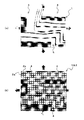
- (B) shows a case where a plurality of support lines intersecting in a lattice pattern are provided so as to intersect with the arrangement direction of the pixel pattern at 45 °. It is a top view which shows one structural example of the support line of the support layer in the said embodiment. It is a top view explaining the effect of the support line of the said support layer, (a) shows the case where there is no support layer, (b) shows the case where there is a support layer. It is a graph which shows the relationship between the wavelength of visible light, and the space
- FIG. It is a figure which shows the other structural example of the support line of the support layer in the said embodiment, (a) shows the generation
- FIG. 1A and 1B are diagrams showing an embodiment of a film-forming mask according to the present invention, in which FIG. 1A is a plan view, FIG. 1B is a centerline sectional view of FIG. 1A, and FIG. d) is a cross-sectional view taken along line AA in (c).
- This film formation mask is for forming a thin film pattern by forming a film on a substrate, and includes a mask layer 1, a support layer 2, and a frame 3.
- the substrate is the display panel 5 of the display device and the thin film pattern is a transparent electrode of the touch panel will be described.
- the thickness of the mask layer 1 affects the darkness of a thin line (hereinafter referred to as “support line 2a”) of the support layer 2 described later formed on the surface of the transparent electrode and the sheet resistance of the transparent electrode.
- the shadow of the support line 2a is a portion located below the support line 2a of the transparent conductive film, and refers to a portion where the film thickness is thinner than the film thickness of other portions. Accordingly, when the difference between the film thickness of the portion located below the support line 2a of the transparent conductive film and the film thickness of the other portion becomes large, the shadow of the support line 2a becomes dark and clear. At the same time, the sheet resistance value of the transparent electrode is increased. On the other hand, when the difference in film thickness is reduced, the shadow of the support line 2a is blurred and thinned. At the same time, the sheet resistance value of the transparent electrode is reduced.
- the gap between the support line 2a and the display surface of the display panel 5 is reduced, and the film forming material that goes around the support line 2a and adheres to the display surface. Less.
- the difference between the film thickness of the portion located below the support line 2a of the transparent conductive film and the film thickness of the other portion increases, and the shadow of the support line 2a formed on the surface of the transparent electrode becomes darker. Become clear. Therefore, moire fringes due to the shadow of the support line 2a are likely to occur, and the sheet resistance value of the transparent electrode increases.
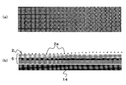
- FIG. 3 is an experimental example showing the occurrence of shadows on the support line 2a when the gap between the support layer 2 and the display surface of the display panel 5 fluctuates.
- the support layer 2 is attracted to the display surface of the display panel 5 by being attracted by the magnet 14 disposed on the back surface of the display panel 5, and the display of the support layer 2 and the display panel 5 as it goes to the right side.
- a case is shown in which a gap is formed between the surface and the gap at the right end is approximately 10 ⁇ m (see FIG. 3B).
- FIG. 3A the shadow of the support line 2a is clearer toward the left side, and the right side of the support line 2a with a gap between the support layer 2 and the display surface of the display panel 5 is formed. The shadow is blurred.
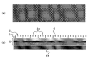
- FIG. 4B when the thickness of the mask layer 1 is increased, the gap between the support line 2a and the display surface of the display panel 5 is increased and goes around the lower side of the support line 2a. As a result, the amount of film forming material adhering to the display surface of the display panel 5 increases. As a result, the difference between the film thickness of the portion located below the support line 2a of the transparent conductive film and the film thickness of the other portion is reduced, and as shown in FIG. The shadow of the support line 2a is blurred and thinned. Therefore, the generation of moire fringes due to the shadow of the support line 2a is suppressed, and the sheet resistance value of the transparent electrode is reduced.
- FIG. 4 is an experimental example showing the occurrence of shadows on the support line 2a when the thickness of the mask layer 1 (the gap between the support layer 2 and the display surface of the display panel 5) is about 40 ⁇ m.
- the sheet resistance value of, for example, an ITO (Indium Tin Oxide) transparent electrode on a touch panel is 40 ⁇ / sq.
- the thickness of the mask layer 1 is appropriately determined by experiment. In the present embodiment, the thickness of the mask layer 1 is set to about 40 ⁇ m.
- the mask layer 1 includes a spacer 6 that is positioned inside the opening pattern 4 and supports the support line 2a of the support layer 2 (see FIGS. 1C and 1D).
- the spacer 6 has the same thickness (about 40 ⁇ m) as the mask layer 1, has an elongated strip shape with a cross section of about 10 ⁇ m ⁇ about 30 ⁇ m, and its long axis intersects the support line 2 a of the support layer 2. (See FIG. 1C). Thereby, the formation position accuracy of the support line 2a of the support layer 2 with respect to the spacer 6 can be relaxed.
- the crossing angle ⁇ 1 between the support line 2a and the spacer 6 is 0 ° ⁇ 1 ⁇ 180 °.
- the spacer 6 is provided so that its long axis coincides with the extending direction of the support line 2a, the spacer is twisted to the support line 2a when the film formation mask is attracted by the magnet 14 and brought into close contact with the display panel 5. May occur and the spacer 6 may tilt. In this case, the support line 2a and the display panel 5 may approach and the shadow of the support line 2a may become noticeable.
- a support layer 2 is provided on one surface 1a of the mask layer 1 so as to cover a region where the opening pattern 4 is surrounded by a broken line in FIG.
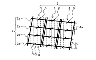
- the support layer 2 is for maintaining the opening pattern 4 in a fixed shape, and has a plurality of support lines 2 a provided across the opening pattern 4.
- it is made of a magnetic metal material such as nickel, nickel alloy, invar or invar alloy.
- the arrangement pitch of the support lines 2a is moire fringes caused by shadows of the support lines 2a transferred onto the transparent electrodes as the film thickness unevenness of the transparent conductive film formed on the display surface of the display panel 5.
- the support line 2a has a plurality of rectangular pixel patterns R formed in a line on the display panel 5 with the display panel 5 and the mask layer 1 positioned.
- G, and B are more preferably arranged so as to intersect each other at an angle ⁇ 2 (0 ° ⁇ 2 ⁇ 180 °) greater than 0 degree and smaller than 180 degrees.
- FIG. 5 is an explanatory diagram showing how the support lines 2a are provided in the arrangement directions of the pixel patterns R, G, and B.
- the mask layer 1 is omitted in order to avoid complication of the drawing.
- FIG. 6A shows a case where a plurality of support lines 2a arranged in parallel intersect with each arrangement direction of the pixel patterns R, G, and B at 90 °
- FIG. A case is shown in which a plurality of support lines 2a intersecting with each other are provided so as to intersect each arrangement direction of pixel patterns R, G, and B at 45 °.
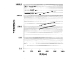
- FIG. 8 is a graph showing the relationship between the wavelength of visible light transmitted through the display surface of the display panel 5 and the interval between generated interference fringes, using the arrangement pitch of the support lines 2a as a parameter.
- the interval between the interference fringes is about 100 ⁇ m to 200 ⁇ m or less, the interference fringes are difficult to be visually recognized. Therefore, according to FIG. 8, it is desirable to set the arrangement pitch of the support lines 2a to 1 mm or more.
- the support layer 2 is not limited to the support line 2 a formed in a mesh shape, and the support line 2 a extends in one direction in the two-dimensional plane on one surface 1 a of the mask layer 1. It may be provided.
- a plurality of support lines 2a having different intervals are set as one set, and a plurality of sets are arranged at a constant arrangement pitch (for example, a long cycle of about 2 mm to 3 mm). There may be. Also by this, generation
- the opening pattern 4 of the mask layer 1 extends in the arrangement direction of the pixel patterns R, G, and B of each color, and the edge of the opening pattern 4 with respect to the color filter formed in a stripe shape.
- the support layer 2 has the striped color filter (pixel pattern).
- a plurality of support lines 2 a intersecting at an angle ⁇ 2 of 0 ° ⁇ 2 ⁇ 180 ° may be arranged in parallel with each other (corresponding to the arrangement directions of R, G, B).
- the generation of moire fringes between the color filter and the transparent electrode is suppressed, and the generation of moire fringes or diffraction fringes between the color filter and the shadow of the support line 2a is also suppressed.
- the generation of moire fringes was suppressed even when the arrangement pitch of the support lines 2a was narrowed to about 500 ⁇ m.
- a frame 3 is provided on one surface 1 a of the mask layer 1.
- the frame 3 holds the mask layer 1 in a state of being stretched parallel to the surface thereof, and is a magnetic metal member such as a frame-like invar or invar alloy having an opening having a size for including the support layer 2.
- the end face 3a and the peripheral edge of the one face 1a of the mask layer 1 are connected by spot welding.
- FIG. 11 is a diagram for explaining the first step, and is a diagram for explaining a mask layer forming step.
- a photoresist 8 is applied to a flat surface on the metal base material 7.
- the photoresist 8 is applied to a thickness of about 40 ⁇ m which is substantially the same as the mask layer 1 to be formed.
- the photoresist 8 is exposed and developed using a photomask, and islands having the same shape and dimensions as the opening pattern 4 corresponding to the opening pattern 4 to be formed are formed.
- a pattern 9 is formed.
- a groove 10 having the same shape and dimension as the spacer 6 is formed inside the island pattern 9 at a depth corresponding to the spacer 6 to be formed and reaching the surface of the metal base material 7.
- an island pattern for alignment marks for alignment with the display panel 5 may be formed at a predetermined position outside the opening pattern formation region.
- the metal base material 7 is dipped in a plating bath of a magnetic metal material such as nickel, and as shown in FIG. A magnetic metal material 11A is formed on the surface of the metal base material 7 to a thickness of about 40 ⁇ m. Thereby, the mask layer 1 is formed on the metal base material 7.
- a magnetic metal material such as nickel
- FIG. 12 is a diagram illustrating the second step, and is an explanatory diagram illustrating a support layer forming step.
- a photoresist 8 is applied on the mask layer 1 formed on the metal base material 7.
- the photoresist 8 is applied to a thickness of about 10 ⁇ m which is substantially the same as the support layer 2 to be formed.
- FIG. 12B is a cross-sectional view taken along the center of the groove 12 extending to the left and right corresponding to the support line 2a.
- the metal base material 7 is immersed in a plating bath of a magnetic metal material such as nickel, and as shown in FIG. 12C, the magnetic metal material of the mask layer 1 exposed in the groove 12 by electroplating.
- the magnetic metal material 11B of the support layer 2 is formed to a thickness of about 10 ⁇ m on the surface of 11A (corresponding to the upper surface of the partition wall 4a of the opening pattern 4 and the upper surface of the spacer 6).
- the mask layer 1 and the support layer 2 are formed on the metal base material 7 by two-stage electroplating.
- the metal base material 7 is washed in a solvent or a stripping solution of the photoresist 8, and the photoresist 8 is dissolved and removed. Further, the mask layer 1 and the support layer 2 are peeled integrally from the metal base material 7.
- the mask sheet 13 shown in FIGS. 1C and 1D is formed in which the mask layer 1 in which the opening pattern 4 and the spacer 6 are formed and the support layer 2 in which the plurality of support lines 2a are formed are integrated. Is done. In this case, when the island pattern for the alignment mark is provided, an opening of the alignment mark is also formed in the mask sheet 13 corresponding to the island pattern.
- FIG. 13 is a diagram for explaining the third step, and is an explanatory diagram showing a frame connection process.
- the mask sheet 13 is The frame 3 is stretched by applying a constant tension to the side parallel to the surface (in the direction of the arrow shown in FIG. 13A).
- the peripheral region of the mask sheet 13 is irradiated with laser light L, and the mask sheet 13 is spot welded to the end surface 3 a of the frame 3. Thereby, the film-forming mask of the present invention is completed.
- the conventional touch panel is manufactured by etching the display panel 5 from both sides with hydrofluoric acid to reduce the thickness and polishing and removing scratches on the surface whose depth has been increased by etching.
- the touch panel does not require high resolution for the pattern of the transparent electrode, and the positional accuracy may be loose. Therefore, in the touch panel according to the present invention, the display panel 5 is etched from both sides with hydrofluoric acid to reduce the thickness, and then the transparent conductive film is formed by sputtering using the film formation mask of the present invention. A transparent electrode is directly formed on the surface.
- the display panel 5 is installed and fixed to the substrate holder in the vacuum chamber of the sputtering film forming apparatus with the display surface as the ITO target side.
- a magnet 14 is built in the substrate holder (see FIG. 9).
- the deposition mask of the present invention is installed and fixed on the mask holder of the sputtering deposition apparatus with the mask layer 1 side as the display panel 5 side.
- the alignment mark formed in advance on the display panel 5 and the alignment mark of the film formation mask are observed and aligned with an imaging camera, and displayed.
- the alignment between the panel 5 and the film formation mask is performed.
- the magnetic force of the magnet 14 built in the substrate holder is applied to the magnetic metal material of the film forming mask, the film forming mask is sucked, and the mask layer 1 is brought into close contact with the display surface of the display panel 5.
- the vacuum chamber lid is closed and the air in the chamber is exhausted until the degree of vacuum in the vacuum chamber reaches a predetermined degree.
- a predetermined amount of rare gas such as argon (Ar) gas is introduced.
- a high voltage is applied between the substrate holder and the target holder holding the ITO target. Thereby, plasma is generated between the display panel 5 and the ITO target, and sputtering of the transparent conductive film is started.
- Argon ions ionized by plasma generation are attracted to the target, collide with the target, and blow off ITO target particles.
- the target particles bounced off fly toward the display panel 5 and accumulate on the display surface of the display panel 5 through a gap between adjacent support lines 2a of the film formation mask.
- a transparent conductive film is formed corresponding to the opening pattern 4 of the mask layer 1, and a transparent electrode of the touch panel is formed.
- the target particles since there is a gap of about 40 ⁇ m, which is the same as the thickness of the mask layer 1, between the support line 2a and the display surface of the display panel 5, the target particles also rotate below the support line 2a. And deposits on the lower display surface of the support line 2a.
- the film thickness of the portion corresponding to the lower side of the support line 2a of the transparent electrode is thinner than the film thickness of other portions. Therefore, the shadow of the support line 2a based on the difference in film thickness is formed on the transparent electrode. Therefore, there is a possibility that moire fringes or diffraction fringes may occur on the display surface due to the shadow of the support line 2a.
- the film forming mask of the present invention at least the arrangement pitch of the support lines 2a generates moire fringes or diffraction fringes due to the shadow of the support lines 2a transferred onto the transparent electrode as the film thickness unevenness of the film forming. Therefore, the generation of the moire fringes or diffraction fringes is suppressed. Therefore, the display quality of the display device using the touch panel of the present invention can be improved.
- the sputtering apparatus forms the film while the substrate and the ITO target are stationary.
- the sputtering apparatus may form the film while relatively moving the substrate and the ITO target.
- the film formation of the transparent conductive film is not limited to sputtering, and other known film formation techniques such as vacuum deposition may be applied.
- the transparent conductive film is not limited to ITO (indium tin oxide), and may be zinc oxide, tin oxide, or the like.
Landscapes
- Chemical & Material Sciences (AREA)
- Engineering & Computer Science (AREA)
- Materials Engineering (AREA)
- Chemical Kinetics & Catalysis (AREA)
- Metallurgy (AREA)
- Organic Chemistry (AREA)
- Electrochemistry (AREA)
- Mechanical Engineering (AREA)
- Theoretical Computer Science (AREA)
- General Engineering & Computer Science (AREA)
- Physics & Mathematics (AREA)
- General Physics & Mathematics (AREA)
- Human Computer Interaction (AREA)
- Physical Vapour Deposition (AREA)
Abstract
本発明は、表示パネル5の表示面上に成膜形成される透明電極に対応して該透明電極と形状寸法の同じ開口パターン4を有するマスク層1と、開口パターン4を横断してマスク層1の一面1aに設けられた複数のサポートライン2aを有するサポート層2と、を備え、サポート層2のサポートライン2aの配列ピッチは、成膜の膜厚むらとして透明電極上に転写されるサポートライン2aの影に起因するモアレ縞又は回折縞の発生を抑制し得る寸法とした。
Description
本発明は、基板上に成膜して薄膜パターンを形成するための成膜マスクに関し、特にタッチパネルを備えた表示装置の表示品質の向上を図り得る成膜マスク、成膜マスクの製造方法及びタッチパネルに係るものである。
従来のこの種の成膜マスクは、少なくとも1つ以上の開口部を有するマスク部分の一方の面に上記開口部を横切るように補強線を接続し、上記マスク部分の他方の面と上記補強線との間に隙間が存在するものとなっていた(例えば、特許文献1参照)。
しかし、このような従来の成膜マスクにおいて、補強線は、開口部を横切って複数の細線を平行に並べて設けただけのものや、メッシュ状に形成しただけのものであり、補強線の配列ピッチには、何ら配慮がなされていなかった。したがって、このような成膜マスクを使用して成膜し、例えばタッチパネルの透明電極を形成した場合には、膜厚むらとして透明電極の表面に転写される上記補強線の影に起因するモアレ縞や回折縞が発生するおそれがあった。それ故、タッチパネルを備えた表示装置の表示品質を低下させるおそれがあった。
そこで、本発明は、このような問題点に対処し、タッチパネルを備えた表示装置の表示品質の向上を図り得る成膜マスク、成膜マスクの製造方法及びタッチパネルを提供することを目的とする。
上記目的を達成するために、本発明による成膜マスクは、基板上に成膜形成される薄膜パターンに対応して該薄膜パターンと形状寸法の同じ開口パターンを有するマスク層と、前記開口パターンを横断して前記マスク層の一面に設けられた複数の細線を有するサポート層と、を備え、前記サポート層の細線の配列ピッチは、成膜の膜厚むらとして前記薄膜パターン上に転写される前記細線の影に起因するモアレ縞又は回折縞の発生を抑制し得る寸法とした。
また、本発明による成膜マスクの製造方法は、基板上に成膜形成される薄膜パターンに対応して、該薄膜パターンと形状寸法の同じ開口パターンを有する磁性金属材料のマスク層を金属母材上に電気めっきにより形成する第1ステップと、前記開口パターンを横断して複数の細線を有する磁性金属材料のサポート層を、前記マスク層の一面に電気めっきにより形成する第2ステップと、を行う成膜マスクの製造方法であって、前記第2ステップは、前記サポート層の細線を、成膜の膜厚むらとして前記薄膜パターン上に転写される前記細線の影に起因するモアレ縞又は回折縞の発生を抑制し得る配列ピッチで形成するものである。
さらに、本発明によるタッチパネルは、成膜形成される透明電極と形状寸法の同じ開口パターンを有するマスク層と、前記開口パターンを横断して前記マスク層の一面に設けられた複数の細線を有するサポート層と、を備えた成膜マスクを使用して、前記サポート層側から表示素子の表示面に成膜形成された透明電極を有するタッチパネルであって、成膜の膜厚むらとして前記透明電極上に転写される前記細線の影の配列ピッチが、該細線の影に起因するモアレ縞又は回折縞の発生を抑制し得る寸法である。
本発明の成膜マスクによれば、成膜の膜厚むらとして薄膜パターン上に転写されるサポート層の細線の影に起因するモアレ縞又は回折縞の発生を抑制することができる。したがって、本発明の成膜マスクを使用してタッチパネルの透明電極を形成した場合にも、表示画面にモアレ縞や回折縞の発生がなく、表示装置の表示品質の向上を図ることができる。
以下、本発明の実施形態を添付図面に基づいて詳細に説明する。図1は本発明による成膜マスクの一実施形態を示す図であり、(a)は平面図、(b)は(a)の中心線断面図、(c)は要部拡大平面図、(d)は(c)のA-A線断面矢視図である。この成膜マスクは、基板上に成膜して薄膜パターンを形成するためのものであり、マスク層1と、サポート層2と、フレーム3と、を備えて構成されている。なお、ここでは、基板が表示装置の表示パネル5であり、薄膜パターンはタッチパネルの透明電極である場合について説明する。
上記マスク層1は、表示パネルの表示面上に成膜形成される透明電極(薄膜パターン)に対応して該透明電極と形状寸法の同じ開口パターン4を有するもので、例えばニッケル、ニッケル合金、インバー又はインバー合金等の磁性金属材料から成る。
図2は上記マスク層1の部分拡大平面図である。同図において、白抜き部分が透明電極に対応した開口パターン4であり、隣接する開口パターン4の隔壁4aの幅は最小10μm程度となっている。なお、詳細には、開口パターン4は、平面積の広い開口部がタッチパネルの電極部に対応し、該電極部から延びる細いライン状開口部が図示省略の制御部に繋がる引き出し線に対応している。
マスク層1の厚みは、透明電極表面に形成される後述のサポート層2の細線(以下「サポートライン2a」という)の影の濃さ及び透明電極のシート抵抗に影響を及ぼす。ここで、上記サポートライン2aの影とは、透明導電膜のサポートライン2aの下側に位置する部分であり、他の部分の膜厚よりも膜厚が薄くなっている部分を言う。したがって、透明導電膜のサポートライン2aの下側に位置する部分の膜厚と他の部分の膜厚との差が大きくなると、サポートライン2aの影は濃くなり明瞭となる。同時に、透明電極のシート抵抗値が大きくなる。一方、上記膜厚の差が小さくなるとサポートライン2aの影はぼやけて薄くなる。同時に、透明電極のシート抵抗値が小さくなる。
詳細には、マスク層1の厚みが薄くなると、サポートライン2aと表示パネル5の表示面との間の隙間が小さくなり、サポートライン2aの下側に回り込んで表示面に付着する成膜材料が少なくなる。これにより、透明導電膜のサポートライン2aの下側に位置する部分の膜厚と他の部分の膜厚との差が大きくなって、透明電極表面に形成されるサポートライン2aの影が濃くなり明瞭になる。したがって、サポートライン2aの影に起因するモアレ縞が発生し易くなると共に、透明電極のシート抵抗値が大きくなる。
図3は、サポート層2と表示パネル5の表示面との間の隙間が変動した場合のサポートライン2aの影の発生状況を示す実験例である。同図において、左側はサポート層2が表示パネル5の裏面に配置された磁石14に吸引されて表示パネル5の表示面に密着しており、右側に行くに従ってサポート層2と表示パネル5の表示面との間に隙間が生じ、右端においてその隙間が約10μmとなっている場合を示す(図3(b)参照)。図3(a)から明らかなように、サポートライン2aの影は、左側程明瞭であり、サポート層2と表示パネル5の表示面との間に隙間が生じている右側程、サポートライン2aの影がぼやけている。
逆に、図4(b)に示すように、マスク層1の厚みが厚くなると、サポートライン2aと表示パネル5の表示面との間の隙間が大きくなり、サポートライン2aの下側に回り込んで表示パネル5の表示面に付着する成膜材料が多くなる。これにより、透明導電膜のサポートライン2aの下側に位置する部分の膜厚と他の部分の膜厚との差が小さくなって、図4(a)に示すように、透明電極表面に形成されるサポートライン2aの影がぼやけて薄くなる。したがって、サポートライン2aの影に起因するモアレ縞の発生が抑制されると共に、透明電極のシート抵抗値が小さくなる。図4はマスク層1の厚み(サポート層2と表示パネル5の表示面との間の隙間)が約40μmである場合の、サポートライン2aの影の発生状況を示した実験例である。
一般に、タッチパネルにおける例えばITO(Indium Tin Oxide)透明電極のシート抵抗値は、40Ω/sq.以下であればよく、マスク層1の厚みは、実験により適宜決定される。本実施形態においては、マスク層1の厚みは、約40μmに設定されている。
上記マスク層1は、開口パターン4の内部に位置してサポート層2のサポートライン2aを下支えするスペーサ6を含んでいる(図1(c),(d)参照)。このスペーサ6は、マスク層1と同じ厚み(約40μm)を有し、横断面が約10μm×約30μmの細長い細片状を成し、その長軸をサポート層2のサポートライン2aと交差させて設けられている(図1(c)参照)。これにより、上記スペーサ6に対するサポート層2のサポートライン2aの形成位置精度を緩和することができる。
また、サポートライン2aとスペーサ6との交差角度θ1は、0°<θ1<180°であるのが望ましい。スペーサ6を、その長軸がサポートライン2aの延設方向に合致するように設けた場合には、成膜マスクを磁石14で吸引して表示パネル5に密着させる際に、サポートライン2aにねじれが生じてスペーサ6が傾く可能性がある。この場合、サポートライン2aと表示パネル5が接近してサポートライン2aの影が顕著になるおそれがある。一方、スペーサ6を、その長軸がサポートライン2aと上記角度θ1で交差するように設けた場合には、サポートライン2aにねじれが生じてもスペーサ6が傾き難くなる。したがって、サポートライン2aが表示パネル5に接近せず、サポートライン2aの影の形成が抑制される。なお、本実施形態においては、θ1=45°としている。
上記マスク層1の一面1aには、図1(a)の破線で囲われた開口パターン4の形成領域を覆ってサポート層2が設けられている。このサポート層2は、開口パターン4を一定形状に維持するためのもので、開口パターン4を横断して設けられた複数のサポートライン2aを有するものである。そして、例えばニッケル、ニッケル合金、インバー又はインバー合金等の磁性金属材料で形成されている。この場合、上記サポートライン2aの配列ピッチは、表示パネル5の表示面上へ成膜される透明導電膜の膜厚むらとして透明電極上に転写される上記サポートライン2aの影に起因するモアレ縞又は回折縞の発生を抑制し得る寸法であるのが望ましい。
さらに、サポートライン2aは、図1(c)に示すように、表示パネル5とマスク層1とが位置決めされた状態で、表示パネル5に一列に並べて形成されている複数の矩形状画素パターンR,G,Bの各配列方向と0度よりも大きく180度よりも小さい角度θ2(0°<θ2<180°)で交差するように設けられるのがより望ましい。図5は、画素パターンR,G,Bの各配列方向に対するサポートライン2aの設け方を示す説明図である。なお、ここでは、図が煩雑になるのを避けるため、マスク層1は省略されている。同図(a)は、平行に並んだ複数のサポートライン2aが画素パターンR,G,Bの各配列方向と90°で交差するように設けた場合を示し、同図(b)は、格子状に交差した複数のサポートライン2aが画素パターンR,G,Bの各配列方向と45°で交差するように設けた場合を示している。これにより、表示パネル5の透明電極に転写されるサポートライン2aの影と画素との干渉が抑制され、モアレの発生が抑制される。
図6はサポート層2のサポートライン2aの一構成例を示す平面図である。同図に示す構成例において、サポート層2は複数のサポートライン2aが縦横に交差してメッシュ状の構成を成している。これにより、図7(a)に示すように、サポートライン2aが設けられていない成膜マスクにおいては、後述のフレーム3にマスク層1を図7(a)に矢印で示すように架張して固定する際に、開口パターン4の形状が崩れてしまうことがあったが、本発明においては、開口パターン4を横断してメッシュ状のサポートライン2aを設けているため、マスク層1及びサポート層2に図7(b)に矢印で示すように張力を与えても開口パターン4の形状が維持される。
図8は表示パネル5の表示面を透過する可視光の波長と発生する干渉縞の間隔との関係を、サポートライン2aの配列ピッチをパラメータとして示すグラフである。一般に、干渉縞の間隔が100μm~200μm程度以下であれば、干渉縞が視認され難くなる。したがって、図8によれば、サポートライン2aの配列ピッチは、1mm以上に設定するのが望ましい。
なお、サポート層2は、図6に示すように、サポートライン2aがメッシュ状に形成されたもの限られず、サポートライン2aがマスク層1の一面1aにて、二次元平面内の一方向に延びて設けられたものであってもよい。この場合、図9(b)に示すように、互いに異なる間隔を有する複数のサポートライン2aを1組として複数組を一定の配列ピッチ(例えば、2mm~3mm程度の長周期)で配置したものであってもよい。これによっても、図9(a)に示すような上記サポートライン2aの影に起因したモアレ縞又は回折縞の発生を抑制することができる。
さらに、マスク層1の開口パターン4が、図10に示すように、各色の画素パターンR,G,Bの配列方向に伸びてストライプ状に形成されたカラーフィルタに対して開口パターン4の縁部(隔壁4a)が平行するのではなく、予め定められた所定角度で交差するように設計された透明電極に対応したものである場合に、サポート層2は、上記ストライプ状のカラーフィルタ(画素パターンR,G,Bの各配列方向に一致)に対して、0°<θ2<180°の角度θ2で交差させた複数のサポートライン2aを平行に配置したものであってもよい。これにより、カラーフィルタと透明電極との間のモアレ縞の発生が抑制されると共に、カラーフィルタとサポートライン2aの影との間のモアレ縞又は回折縞の発生も抑制される。また、この場合、サポートライン2aの配列ピッチは、500μm程度に狭くしてもモアレ縞の発生が抑制された。
上記マスク層1の一面1aには、フレーム3が設けられている。このフレーム3は、マスク層1をその面に平行に張った状態で保持するものであり、サポート層2を内包する大きさの開口部を有する枠状のインバー又はインバー合金等の磁性金属部材であり、その端面3aとマスク層1の一面1aの周縁部とがスポット溶接して接続されている。
次に、このように構成された成膜マスクの製造方法について説明する。
本発明の成膜マスクは、表示パネル5の表示面上に成膜形成される透明電極に対応して、該透明電極と形状寸法の同じ開口パターン4を有する磁性金属材料のマスク層1を金属母材上に電気めっきにより形成する第1ステップと、上記開口パターン4を横断して複数のサポートライン2aを有する磁性金属材料のサポート層2を、上記マスク層1の一面1aに電気めっきにより形成する第2ステップと、上記マスク層1の一面1aの周縁部を枠状のフレーム3に接続する第3ステップとを行って製造される。以下、各ステップを詳細に説明する。
本発明の成膜マスクは、表示パネル5の表示面上に成膜形成される透明電極に対応して、該透明電極と形状寸法の同じ開口パターン4を有する磁性金属材料のマスク層1を金属母材上に電気めっきにより形成する第1ステップと、上記開口パターン4を横断して複数のサポートライン2aを有する磁性金属材料のサポート層2を、上記マスク層1の一面1aに電気めっきにより形成する第2ステップと、上記マスク層1の一面1aの周縁部を枠状のフレーム3に接続する第3ステップとを行って製造される。以下、各ステップを詳細に説明する。
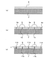
図11は上記第1ステップを説明する図で、マスク層形成工程を示す説明図である。
先ず、図11(a)に示すように、金属母材7上の平坦面にフォトレジスト8が塗布される。このとき、フォトレジスト8は、形成しようとするマスク層1と略同じ40μm程度の厚みに塗布される。
先ず、図11(a)に示すように、金属母材7上の平坦面にフォトレジスト8が塗布される。このとき、フォトレジスト8は、形成しようとするマスク層1と略同じ40μm程度の厚みに塗布される。
次に、図11(b)に示すように、フォトマスクを使用して上記フォトレジスト8を露光及び現像し、形成しようとする開口パターン4に対応して該開口パターン4と形状寸法の同じ島パターン9を形成する。同時に、島パターン9の内側には、形成しようとするスペーサ6に対応して該スペーサ6と形状寸法の同じ溝10が金属母材7の表面に達する深さで形成される。また、開口パターン形成領域外の予め定められた位置に、表示パネル5と位置合わせするためのアライメントマーク用の島パターンを形成してもよい。
続いて、上記金属母材7をニッケル等の磁性金属材料のめっき浴に浸漬し、図11(c)に示すように、電気めっきにより上記島パターン9の外側9a及び溝10内に剥き出しとなった金属母材7の表面に磁性金属材料11Aを40μm程度の厚みに形成する。これにより、金属母材7上にマスク層1が形成される。
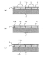
図12は上記第2ステップを説明する図で、サポート層形成工程を示す説明図である。
先ず、図12(a)に示すように、上記金属母材7上に形成されたマスク層1上にフォトレジスト8が塗布される。このとき、フォトレジスト8は、形成しようとするサポート層2と略同じ10μm程度の厚みに塗布される。
先ず、図12(a)に示すように、上記金属母材7上に形成されたマスク層1上にフォトレジスト8が塗布される。このとき、フォトレジスト8は、形成しようとするサポート層2と略同じ10μm程度の厚みに塗布される。
次に、図12(b)に示すように、フォトマスクを使用して上記フォトレジスト8を露光及び現像し、図1(c)に示すような例えば縦横に交差して延びるサポートライン2aに対応して、該サポートライン2aと形状寸法の同じ溝12を上記マスク層1に達する深さで形成する。なお、図12(b)は、サポートライン2aに対応して左右に延びる溝12の中央位置で切断した断面図である。
次いで、上記金属母材7をニッケル等の磁性金属材料のめっき浴に浸漬し、図12(c)に示すように、電気めっきにより上記溝12内に剥き出しとなったマスク層1の磁性金属材料11Aの表面(開口パターン4の隔壁4aの上面及びスペーサ6の上面に相当)にサポート層2の磁性金属材料11Bを10μm程度の厚みに形成する。これにより、金属母材7上にマスク層1とサポート層2とが2段階の電気めっきにより形成される。
この後、金属母材7を溶剤中又はフォトレジスト8の剥離液中で洗浄し、フォトレジスト8を溶解させて除去する。さらに、金属母材7からマスク層1とサポート層2とを一体的に剥離する。これにより、開口パターン4及びスペーサ6を形成したマスク層1と、複数のサポートライン2aを形成したサポート層2とが一体となった図1(c),(d)に示すマスクシート13が形成される。この場合、アライメントマーク用の島パターンが設けられているときには、マスクシート13には、上記島パターンに対応してアライメントマークの開口も形成される。
図13は上記第3ステップを説明する図で、フレーム接続工程を示す説明図である。
先ず、図13(a)に示すように、一面1aにサポート層2を備えたマスク層1の該一面1aと枠状のフレーム3の端面3aとを対面させた状態で、マスクシート13をその面に平行な側方(図13(a)に示す矢印方向)に一定の張力を与えてフレーム3に架張する。
先ず、図13(a)に示すように、一面1aにサポート層2を備えたマスク層1の該一面1aと枠状のフレーム3の端面3aとを対面させた状態で、マスクシート13をその面に平行な側方(図13(a)に示す矢印方向)に一定の張力を与えてフレーム3に架張する。
続いて、図13(b)に示すように、マスクシート13の周縁領域にレーザ光Lを照射し、マスクシート13をフレーム3の端面3aにスポット溶接する。これにより、本発明の成膜マスクが完成する。
次に、本発明による成膜マスクを使用したタッチパネルの製造について説明する。
従来のタッチパネルの製造は、表示パネル5をフッ酸により両面からエッチングして厚みを減じると共に、エッチングにより深さを増した表面の傷を研磨して除去する工程と、表示面の全面にITOの透明導電膜をスパッタリングして形成する工程と、該透明導電膜上にフォトレジストを塗布し、フォトマスクを使用して露光及び現像してレジストマスクを形成する工程と、該レジストマスクを使用して上記透明導電膜をエッチングし、透明電極を形成する工程とを実施するものであった。したがって、製造工程が複雑でランニングコストが高くなるという問題があった。
従来のタッチパネルの製造は、表示パネル5をフッ酸により両面からエッチングして厚みを減じると共に、エッチングにより深さを増した表面の傷を研磨して除去する工程と、表示面の全面にITOの透明導電膜をスパッタリングして形成する工程と、該透明導電膜上にフォトレジストを塗布し、フォトマスクを使用して露光及び現像してレジストマスクを形成する工程と、該レジストマスクを使用して上記透明導電膜をエッチングし、透明電極を形成する工程とを実施するものであった。したがって、製造工程が複雑でランニングコストが高くなるという問題があった。
タッチパネルは、透明電極のパターンに高解像力は要求されず、且つ位置精度も緩くてよい。そこで、本発明によるタッチパネルは、表示パネル5をフッ酸により両面からエッチングして厚みを減じた後、本発明の成膜マスクを使用して透明導電膜をスパッタリング成膜し、表示パネル5の表示面に透明電極を直接形成したものである。
なお、本発明によるタッチパネルの製造においては、表示パネル5の表面の傷は、透明電極の形成に何ら悪影響を及ぼさないため、エッチングにより深さを増した表面の傷を除去するための研磨工程を省略することができる。したがって、本発明によるタッチパネルの製造においては、従来の製造方法に比べて製造工程が短縮でき、ランニングコストを低減することができる効果がある。
以下、本発明によるタッチパネルの製造について、特に透明電極の形成工程を詳細に説明する。
先ず、例えばスパッタリング成膜装置の真空チャンバー内の基板ホルダーに、表示パネル5が表示面をITOターゲット側として設置され、固定される。この場合、基板ホルダーには磁石14が内蔵されている(図9参照)。
先ず、例えばスパッタリング成膜装置の真空チャンバー内の基板ホルダーに、表示パネル5が表示面をITOターゲット側として設置され、固定される。この場合、基板ホルダーには磁石14が内蔵されている(図9参照)。
一方、上記スパッタリング成膜装置のマスクホルダーには、本発明の成膜マスクがマスク層1側を表示パネル5側として設置され、固定される。
次に、表示パネル5と成膜マスクとを対面させた状態で、例えば表示パネル5に予め形成されたアライメントマークと、成膜マスクのアライメントマークとを撮像カメラにより観察して位置合わせし、表示パネル5と成膜マスクとのアライメントが行われる。
続いて、基板ホルダーに内蔵された磁石14の磁力を成膜マスクの磁性金属材料に作用させて、成膜マスクを吸引し、表示パネル5の表示面にマスク層1を密着させる。
その後、真空チャンバーの蓋を閉じて、真空チャンバー内の真空度が所定の真空度となるまでチャンバー内の空気を排気する。チャンバー内の真空度が所定の真空度に達すると、所定量の例えばアルゴン(Ar)ガス等の希ガスが導入される。そして、基板ホルダーと、ITOターゲットを保持したターゲットホルダーとの間に高電圧が付与される。これにより、表示パネル5とITOターゲットとの間にプラズマが生成され、透明導電膜のスパッタリングが開始される。
プラズマの生成によりイオン化されたアルゴンイオンは、ターゲット側に引き寄せられてターゲットに衝突し、ITOのターゲット粒子を弾き飛ばす。弾き飛ばされたターゲット粒子は、表示パネル5に向かって飛翔し、成膜マスクの隣接するサポートライン2aの隙間を通って表示パネル5の表示面に堆積する。これにより、表示パネル5の表示面上には、マスク層1の開口パターン4に対応して透明導電膜が成膜され、タッチパネルの透明電極が形成される。この場合、上記サポートライン2aと表示パネル5の表示面との間には、マスク層1の厚みと同じ約40μmの隙間が存在するため、上記ターゲット粒子は、サポートライン2aの下側にも回り込んで、サポートライン2aの下側の表示面にも堆積する。
上記透明電極のサポートライン2aの下側に対応した部分の膜厚は、他の部分の膜厚よりも薄い。したがって、透明電極には、上記膜厚の差に基づくサポートライン2aの影が形成されることになる。それ故、このサポートライン2aの影に起因して表示面には、モアレ縞又は回折縞が発生するおそれがある。しかし、本発明の成膜マスクは、少なくとも、上記サポートライン2aの配列ピッチが、成膜の膜厚むらとして透明電極上に転写されるサポートライン2aの影に起因するモアレ縞又は回折縞の発生を抑制し得る寸法とされているため、上記モアレ縞又は回折縞の発生が抑制される。したがって、本発明のタッチパネルを使用した表示装置の表示品質を向上することができる。
なお、上記実施形態において、スパッタリング装置は、基板とITOターゲットとを静止させて成膜するものであるが、基板とITOターゲットとを相対的に移動しながら成膜するものであってもよい。また、透明導電膜の成膜は、スパッタリングに限られず、真空蒸着等、他の公知の成膜技術が適用されてもよい。さらに、透明導電膜は、ITO(酸化インジウム・スズ)に限られず、酸化亜鉛や、酸化スズ等であってもよい。
また、上記実施形態においては、成膜マスクがフレーム3を備えたものである場合について説明したが、本発明はこれに限られず、フレーム3は無くてもよい。この場合、マスクシート13をその面に平行な側方に一定のテンションをかけた状態でマスクホルダーに保持するとよい。
1…マスク層
1a…マスク層の一面
2…サポート層
2a…サポートライン(細線)
4…開口パターン
5…表示パネル(基板又は表示素子)
6…スペーサ
7…金属母材
14…磁石
R…赤色対応画素パターンの配列
G…緑色対応画素パターンの配列
B…青色対応画素パターンの配列
1a…マスク層の一面
2…サポート層
2a…サポートライン(細線)
4…開口パターン
5…表示パネル(基板又は表示素子)
6…スペーサ
7…金属母材
14…磁石
R…赤色対応画素パターンの配列
G…緑色対応画素パターンの配列
B…青色対応画素パターンの配列
Claims (12)
- 基板上に成膜形成される薄膜パターンに対応して該薄膜パターンと形状寸法の同じ開口パターンを有するマスク層と、
前記開口パターンを横断して前記マスク層の一面に設けられた複数の細線を有するサポート層と、
を備え、
前記サポート層の細線の配列ピッチは、成膜の膜厚むらとして前記薄膜パターン上に転写される前記細線の影に起因するモアレ縞又は回折縞の発生を抑制し得る寸法であることを特徴とする成膜マスク。 - 前記サポート層の細線は、前記基板と前記マスク層とが位置決めされた状態で、前記基板上に一列に並べて形成されている複数の矩形状パターンの配列方向と0度よりも大きく180度よりも小さい角度で交差するように設けられていることを特徴とする請求項1記載の成膜マスク。
- 前記サポート層の細線は、前記マスク層の一面にて、二次元平面内の一方向に延びて設けられていることを特徴とする請求項1又は2記載の成膜マスク。
- 前記サポート層の細線は、互いに異なる間隔を有する複数の細線を1組として複数組を一定の配列ピッチで配置したものであることを特徴とする請求項1又は2記載の成膜マスク。
- 前記マスク層は、前記開口パターンの内部に位置して前記サポート層の細線を下支えするスペーサを含むことを特徴とする請求項1又は2記載の成膜マスク。
- 前記スペーサは、細長い細片状を成し、その長軸を前記サポート層の細線と交差させて設けられていることを特徴とする請求項5記載の成膜マスク。
- 前記マスク層と前記サポート層とは、磁性金属材料の2段階電気めっきにより形成されたものであることを特徴とする請求項1又は2記載の成膜マスク。
- 基板上に成膜形成される薄膜パターンに対応して、該薄膜パターンと形状寸法の同じ開口パターンを有する磁性金属材料のマスク層を金属母材上に電気めっきにより形成する第1ステップと、
前記開口パターンを横断して複数の細線を有する磁性金属材料のサポート層を、前記マスク層の一面に電気めっきにより形成する第2ステップと、
を行う成膜マスクの製造方法であって、
前記第2ステップは、前記サポート層の細線を、成膜の膜厚むらとして前記薄膜パターン上に転写される前記細線の影に起因するモアレ縞又は回折縞の発生を抑制し得る配列ピッチで形成することを特徴とする成膜マスクの製造方法。 - 前記マスク層は、前記開口パターンの内部に位置して前記サポート層の細線を下支えするスペーサを含むことを特徴とする請求項8記載の成膜マスクの製造方法。
- 成膜形成される透明電極と形状寸法の同じ開口パターンを有するマスク層と、前記開口パターンを横断して前記マスク層の一面に設けられた複数の細線を有するサポート層と、を備えた成膜マスクを使用して、前記サポート層側から表示素子の表示面に成膜形成された透明電極を有するタッチパネルであって、
成膜の膜厚むらとして前記透明電極上に転写される前記細線の影の配列ピッチが、該細線の影に起因するモアレ縞又は回折縞の発生を抑制し得る寸法であることを特徴とするタッチパネル。 - 前記細線の影は、前記表示素子に一列に並べて形成されている複数の画素パターンの配列方向と0度よりも大きく180度よりも小さい角度で交差していることを特徴とする請求項10記載のタッチパネル。
- 前記成膜マスクの前記マスク層及び前記サポート層は、磁性金属材料の2段階めっきにより形成されたものであり、
前記透明電極は、前記表示素子の前記表示面とは反対側に配置された磁石により前記成膜マスクを吸引して、前記マスク層を前記表示面に密着させた状態で成膜形成されることを特徴とする請求項10又は11記載のタッチパネル。
Priority Applications (3)
| Application Number | Priority Date | Filing Date | Title |
|---|---|---|---|
| CN201580036959.3A CN106488995B (zh) | 2014-07-08 | 2015-06-26 | 成膜掩模、成膜掩模的制造方法和触摸面板 |
| KR1020167035071A KR20170028311A (ko) | 2014-07-08 | 2015-06-26 | 성막 마스크, 성막 마스크의 제조 방법 및 터치 패널 |
| US15/359,527 US10533246B2 (en) | 2014-07-08 | 2016-11-22 | Deposition mask, method for manufacturing the same, and touch panel |
Applications Claiming Priority (2)
| Application Number | Priority Date | Filing Date | Title |
|---|---|---|---|
| JP2014-140709 | 2014-07-08 | ||
| JP2014140709A JP6303154B2 (ja) | 2014-07-08 | 2014-07-08 | 成膜マスク、その製造方法及びタッチパネル |
Related Child Applications (1)
| Application Number | Title | Priority Date | Filing Date |
|---|---|---|---|
| US15/359,527 Continuation US10533246B2 (en) | 2014-07-08 | 2016-11-22 | Deposition mask, method for manufacturing the same, and touch panel |
Publications (1)
| Publication Number | Publication Date |
|---|---|
| WO2016006480A1 true WO2016006480A1 (ja) | 2016-01-14 |
Family
ID=55064118
Family Applications (1)
| Application Number | Title | Priority Date | Filing Date |
|---|---|---|---|
| PCT/JP2015/068514 Ceased WO2016006480A1 (ja) | 2014-07-08 | 2015-06-26 | 成膜マスク、成膜マスクの製造方法及びタッチパネル |
Country Status (6)
| Country | Link |
|---|---|
| US (1) | US10533246B2 (ja) |
| JP (1) | JP6303154B2 (ja) |
| KR (1) | KR20170028311A (ja) |
| CN (1) | CN106488995B (ja) |
| TW (1) | TW201626187A (ja) |
| WO (1) | WO2016006480A1 (ja) |
Cited By (1)
| Publication number | Priority date | Publication date | Assignee | Title |
|---|---|---|---|---|
| CN111220320A (zh) * | 2020-03-03 | 2020-06-02 | 中科九微科技有限公司 | 陶瓷电极、具有其的薄膜传感器及该陶瓷电极的制作方法 |
Families Citing this family (9)
| Publication number | Priority date | Publication date | Assignee | Title |
|---|---|---|---|---|
| KR102618039B1 (ko) * | 2018-08-29 | 2023-12-27 | 삼성디스플레이 주식회사 | 마스크 조립체, 이를 포함한 표시 장치의 제조장치 및 표시 장치의 제조방법 |
| US11493765B2 (en) * | 2019-06-14 | 2022-11-08 | Flir Systems Ab | Image relay systems and methods for wearable apparatuses |
| KR102792162B1 (ko) | 2019-09-16 | 2025-04-07 | 삼성디스플레이 주식회사 | 증착 마스크, 증착 마스크의 제조 방법 |
| WO2021092759A1 (zh) * | 2019-11-12 | 2021-05-20 | 京东方科技集团股份有限公司 | 掩模板 |
| KR102895634B1 (ko) * | 2020-01-15 | 2025-12-05 | 삼성디스플레이 주식회사 | 마스크 |
| KR102787865B1 (ko) | 2020-02-21 | 2025-04-01 | 삼성디스플레이 주식회사 | 표시 장치의 제조장치, 마스크 어셈블리의 제조방법, 및 표시 장치의 제조방법 |
| KR102929156B1 (ko) * | 2020-08-31 | 2026-02-24 | 삼성디스플레이 주식회사 | 마스크, 이의 제조 방법, 및 표시 패널 제조 방법 |
| JP7687291B2 (ja) * | 2022-07-08 | 2025-06-03 | トヨタ自動車株式会社 | 金属皮膜の成膜方法 |
| KR20240042288A (ko) * | 2022-09-23 | 2024-04-02 | 삼성디스플레이 주식회사 | 마스크 장치 및 마스크 장치를 이용한 레진의 도포 방법 |
Citations (3)
| Publication number | Priority date | Publication date | Assignee | Title |
|---|---|---|---|---|
| JPH10330910A (ja) * | 1997-06-04 | 1998-12-15 | Toray Ind Inc | シャドーマスクおよびその製造方法 |
| JPH11214154A (ja) * | 1997-10-15 | 1999-08-06 | Toray Ind Inc | 有機電界発光装置の製造方法 |
| JP2011154338A (ja) * | 2009-09-02 | 2011-08-11 | Sony Corp | 透明導電性電極、タッチパネル、情報入力装置、および表示装置 |
Family Cites Families (11)
| Publication number | Priority date | Publication date | Assignee | Title |
|---|---|---|---|---|
| US3206322A (en) * | 1960-10-31 | 1965-09-14 | Morgan John Robert | Vacuum deposition means and methods for manufacture of electronic components |
| JPH10330911A (ja) * | 1997-06-05 | 1998-12-15 | Toray Ind Inc | シャドーマスクおよびその製造方法 |
| KR100330910B1 (ko) | 1999-03-16 | 2002-04-03 | 홍승현 | 단백질을 이용한 장식품 |
| JP2004318899A (ja) * | 2004-05-26 | 2004-11-11 | Idemitsu Kosan Co Ltd | タッチパネル |
| JP4692290B2 (ja) * | 2006-01-11 | 2011-06-01 | セイコーエプソン株式会社 | マスクおよび成膜方法 |
| KR100775846B1 (ko) * | 2006-09-04 | 2007-11-13 | 엘지전자 주식회사 | 디스플레이 소자 제조용 마스크 |
| JP5007602B2 (ja) * | 2007-05-09 | 2012-08-22 | セイコーエプソン株式会社 | エレクトロルミネッセンス装置及び電子機器 |
| US8553207B2 (en) * | 2008-12-31 | 2013-10-08 | Asml Holdings N.V. | Optically compensated unidirectional reticle bender |
| US9246101B2 (en) * | 2010-03-09 | 2016-01-26 | Sharp Kabushiki Kaisha | Deposition mask, deposition apparatus, and deposition method |
| CN103207518A (zh) * | 2012-01-16 | 2013-07-17 | 昆山允升吉光电科技有限公司 | 防止下垂的掩模框架及防止下垂的掩模组件 |
| CN103268057B (zh) * | 2013-04-28 | 2014-12-17 | 京东方科技集团股份有限公司 | 掩模系统、掩模方法、曝光系统和曝光方法 |
-
2014
- 2014-07-08 JP JP2014140709A patent/JP6303154B2/ja not_active Expired - Fee Related
-
2015
- 2015-06-26 CN CN201580036959.3A patent/CN106488995B/zh not_active Expired - Fee Related
- 2015-06-26 WO PCT/JP2015/068514 patent/WO2016006480A1/ja not_active Ceased
- 2015-06-26 KR KR1020167035071A patent/KR20170028311A/ko not_active Withdrawn
- 2015-07-06 TW TW104121798A patent/TW201626187A/zh unknown
-
2016
- 2016-11-22 US US15/359,527 patent/US10533246B2/en not_active Expired - Fee Related
Patent Citations (3)
| Publication number | Priority date | Publication date | Assignee | Title |
|---|---|---|---|---|
| JPH10330910A (ja) * | 1997-06-04 | 1998-12-15 | Toray Ind Inc | シャドーマスクおよびその製造方法 |
| JPH11214154A (ja) * | 1997-10-15 | 1999-08-06 | Toray Ind Inc | 有機電界発光装置の製造方法 |
| JP2011154338A (ja) * | 2009-09-02 | 2011-08-11 | Sony Corp | 透明導電性電極、タッチパネル、情報入力装置、および表示装置 |
Cited By (1)
| Publication number | Priority date | Publication date | Assignee | Title |
|---|---|---|---|---|
| CN111220320A (zh) * | 2020-03-03 | 2020-06-02 | 中科九微科技有限公司 | 陶瓷电极、具有其的薄膜传感器及该陶瓷电极的制作方法 |
Also Published As
| Publication number | Publication date |
|---|---|
| CN106488995A (zh) | 2017-03-08 |
| KR20170028311A (ko) | 2017-03-13 |
| TW201626187A (zh) | 2016-07-16 |
| US10533246B2 (en) | 2020-01-14 |
| JP2016017207A (ja) | 2016-02-01 |
| CN106488995B (zh) | 2019-11-08 |
| JP6303154B2 (ja) | 2018-04-04 |
| US20170130321A1 (en) | 2017-05-11 |
Similar Documents
| Publication | Publication Date | Title |
|---|---|---|
| JP6303154B2 (ja) | 成膜マスク、その製造方法及びタッチパネル | |
| US12310107B2 (en) | Array substrate and manufacturing method thereof, display device, and mask | |
| CN108118289B (zh) | 用于沉积的掩模及其制造方法 | |
| JP4959631B2 (ja) | グレースケールマスク | |
| WO2016129534A1 (ja) | 蒸着マスクの製造方法および蒸着マスク | |
| JP2013245392A (ja) | 蒸着マスク及び蒸着マスクの製造方法 | |
| CN106098701B (zh) | 一种阵列基板及其制备方法和显示装置 | |
| JP7557582B2 (ja) | 表示装置の製造方法 | |
| JP2012242840A (ja) | カラーフィルタ基板及びその製造方法 | |
| JP2016148113A (ja) | 蒸着マスクの製造方法および蒸着マスク | |
| KR20160145607A (ko) | 성막 마스크, 성막 마스크의 제조 방법 및 터치 패널의 제조 방법 | |
| JP2015028194A (ja) | 成膜マスクの製造方法、成膜マスク及びタッチパネル基板 | |
| KR20250123846A (ko) | 마스크 및 마스크의 제조 방법 | |
| WO2020216009A1 (zh) | 显示基板及其制备方法、显示面板 | |
| CN111061079A (zh) | 一种阵列基板及其制备方法、显示装置 | |
| JP2017150038A (ja) | シャドーマスク及び表示装置の製造方法 | |
| CN102681714B (zh) | 触摸感应器的制造方法及显示设备 | |
| CN109188854B (zh) | 掩膜板、显示基板及其制作方法、显示装置 | |
| CN115963664B (zh) | 一种阵列基板、掩膜板和显示面板 | |
| WO2016093139A1 (ja) | メタルマスク、タッチパネル及びタッチパネルの製造方法 | |
| CN105527801B (zh) | 一种膜层的图案化方法、基板及其制作方法、显示装置 | |
| CN109686662B (zh) | 薄膜晶体管的栅极制作方法 | |
| US8013524B2 (en) | Organic EL display | |
| KR100713893B1 (ko) | 액정표시장치의 제조방법 | |
| CN103943565B (zh) | 一种裸眼3d功能面板的制造方法 |
Legal Events
| Date | Code | Title | Description |
|---|---|---|---|
| 121 | Ep: the epo has been informed by wipo that ep was designated in this application |
Ref document number: 15818224 Country of ref document: EP Kind code of ref document: A1 |
|
| ENP | Entry into the national phase |
Ref document number: 20167035071 Country of ref document: KR Kind code of ref document: A |
|
| NENP | Non-entry into the national phase |
Ref country code: DE |
|
| 122 | Ep: pct application non-entry in european phase |
Ref document number: 15818224 Country of ref document: EP Kind code of ref document: A1 |