WO2016002801A1 - 半導体積層構造体及び半導体素子 - Google Patents
半導体積層構造体及び半導体素子 Download PDFInfo
- Publication number
- WO2016002801A1 WO2016002801A1 PCT/JP2015/068881 JP2015068881W WO2016002801A1 WO 2016002801 A1 WO2016002801 A1 WO 2016002801A1 JP 2015068881 W JP2015068881 W JP 2015068881W WO 2016002801 A1 WO2016002801 A1 WO 2016002801A1
- Authority
- WO
- WIPO (PCT)
- Prior art keywords
- layer
- substrate
- nitride semiconductor
- semiconductor
- gan
- Prior art date
- Legal status (The legal status is an assumption and is not a legal conclusion. Google has not performed a legal analysis and makes no representation as to the accuracy of the status listed.)
- Ceased
Links
Images













Classifications
-
- H—ELECTRICITY
- H10—SEMICONDUCTOR DEVICES; ELECTRIC SOLID-STATE DEVICES NOT OTHERWISE PROVIDED FOR
- H10D—INORGANIC ELECTRIC SEMICONDUCTOR DEVICES
- H10D10/00—Bipolar junction transistors [BJT]
- H10D10/80—Heterojunction BJTs
-
- H—ELECTRICITY
- H10—SEMICONDUCTOR DEVICES; ELECTRIC SOLID-STATE DEVICES NOT OTHERWISE PROVIDED FOR
- H10D—INORGANIC ELECTRIC SEMICONDUCTOR DEVICES
- H10D30/00—Field-effect transistors [FET]
- H10D30/60—Insulated-gate field-effect transistors [IGFET]
-
- H—ELECTRICITY
- H10—SEMICONDUCTOR DEVICES; ELECTRIC SOLID-STATE DEVICES NOT OTHERWISE PROVIDED FOR
- H10D—INORGANIC ELECTRIC SEMICONDUCTOR DEVICES
- H10D30/00—Field-effect transistors [FET]
- H10D30/80—FETs having rectifying junction gate electrodes
- H10D30/83—FETs having PN junction gate electrodes
-
- H—ELECTRICITY
- H10—SEMICONDUCTOR DEVICES; ELECTRIC SOLID-STATE DEVICES NOT OTHERWISE PROVIDED FOR
- H10D—INORGANIC ELECTRIC SEMICONDUCTOR DEVICES
- H10D30/00—Field-effect transistors [FET]
- H10D30/80—FETs having rectifying junction gate electrodes
- H10D30/87—FETs having Schottky gate electrodes, e.g. metal-semiconductor FETs [MESFET]
-
- H—ELECTRICITY
- H10—SEMICONDUCTOR DEVICES; ELECTRIC SOLID-STATE DEVICES NOT OTHERWISE PROVIDED FOR
- H10D—INORGANIC ELECTRIC SEMICONDUCTOR DEVICES
- H10D64/00—Electrodes of devices having potential barriers
- H10D64/01—Manufacture or treatment
- H10D64/011—Manufacture or treatment of electrodes ohmically coupled to a semiconductor
-
- H—ELECTRICITY
- H10—SEMICONDUCTOR DEVICES; ELECTRIC SOLID-STATE DEVICES NOT OTHERWISE PROVIDED FOR
- H10D—INORGANIC ELECTRIC SEMICONDUCTOR DEVICES
- H10D64/00—Electrodes of devices having potential barriers
- H10D64/20—Electrodes characterised by their shapes, relative sizes or dispositions
- H10D64/27—Electrodes not carrying the current to be rectified, amplified, oscillated or switched, e.g. gates
-
- H—ELECTRICITY
- H10—SEMICONDUCTOR DEVICES; ELECTRIC SOLID-STATE DEVICES NOT OTHERWISE PROVIDED FOR
- H10D—INORGANIC ELECTRIC SEMICONDUCTOR DEVICES
- H10D64/00—Electrodes of devices having potential barriers
- H10D64/60—Electrodes characterised by their materials
- H10D64/64—Electrodes comprising a Schottky barrier to a semiconductor
-
- H—ELECTRICITY
- H10—SEMICONDUCTOR DEVICES; ELECTRIC SOLID-STATE DEVICES NOT OTHERWISE PROVIDED FOR
- H10D—INORGANIC ELECTRIC SEMICONDUCTOR DEVICES
- H10D64/00—Electrodes of devices having potential barriers
- H10D64/60—Electrodes characterised by their materials
- H10D64/66—Electrodes having a conductor capacitively coupled to a semiconductor by an insulator, e.g. MIS electrodes
-
- H—ELECTRICITY
- H10—SEMICONDUCTOR DEVICES; ELECTRIC SOLID-STATE DEVICES NOT OTHERWISE PROVIDED FOR
- H10D—INORGANIC ELECTRIC SEMICONDUCTOR DEVICES
- H10D8/00—Diodes
- H10D8/60—Schottky-barrier diodes
-
- H—ELECTRICITY
- H10—SEMICONDUCTOR DEVICES; ELECTRIC SOLID-STATE DEVICES NOT OTHERWISE PROVIDED FOR
- H10H—INORGANIC LIGHT-EMITTING SEMICONDUCTOR DEVICES HAVING POTENTIAL BARRIERS
- H10H20/00—Individual inorganic light-emitting semiconductor devices having potential barriers, e.g. light-emitting diodes [LED]
- H10H20/80—Constructional details
- H10H20/81—Bodies
- H10H20/815—Bodies having stress relaxation structures, e.g. buffer layers
-
- H—ELECTRICITY
- H10—SEMICONDUCTOR DEVICES; ELECTRIC SOLID-STATE DEVICES NOT OTHERWISE PROVIDED FOR
- H10H—INORGANIC LIGHT-EMITTING SEMICONDUCTOR DEVICES HAVING POTENTIAL BARRIERS
- H10H20/00—Individual inorganic light-emitting semiconductor devices having potential barriers, e.g. light-emitting diodes [LED]
- H10H20/80—Constructional details
- H10H20/81—Bodies
- H10H20/822—Materials of the light-emitting regions
- H10H20/824—Materials of the light-emitting regions comprising only Group III-V materials, e.g. GaP
- H10H20/825—Materials of the light-emitting regions comprising only Group III-V materials, e.g. GaP containing nitrogen, e.g. GaN
Definitions
- the present invention relates to a semiconductor multilayer structure and a semiconductor element.
- Patent Document 1 As a conventional light-emitting element, one formed by growing a crystal film on a surface of a translucent substrate on which a concavo-convex pattern is formed is known (for example, see Patent Document 1).
- Patent Document 1 a GaN-based semiconductor layer is grown on the surface of the sapphire substrate on which the concavo-convex pattern is formed.
- the concavo-convex pattern of the sapphire substrate of Patent Document 1 is emitted from the light emitting layer in the GaN-based semiconductor layer due to the difference in refractive index between the sapphire substrate and the GaN-based semiconductor layer at the interface between the sapphire substrate and the GaN-based semiconductor layer. It has a function of suppressing reflection of emitted light. By suppressing such reflection, absorption of reflected light by the light emitting layer and attenuation due to multiple reflection of reflected light can be reduced, and the light extraction efficiency of the light emitting element can be improved.
- the GaN-based semiconductor layer grows also from the side wall of the processed portion.
- a crystal having a c-axis in the vertical direction of the substrate and a crystal having a c-axis other than the vertical direction are mixed, and the GaN-based semiconductor layer becomes polycrystalline.
- the quality of the nitride semiconductor layer is remarkably deteriorated (see, for example, Patent Document 2).
- the present invention has been made in view of such circumstances, and an object of the present invention is to provide a semiconductor laminated structure having a nitride semiconductor layer having high quality on the gallium oxide substrate and high uniformity in the plane. And a semiconductor element including the semiconductor multilayer structure.
- One embodiment of the present invention provides a semiconductor stacked structure according to [1] to [5] in order to achieve the above object.
- the Ga 2 O 3 is formed so as to contact with the upper surface part on the substrate, the dielectric difference in refractive index between the Ga 2 O 3 substrate is 0.15 or less
- a buffer layer made of a GaN crystal so as to be in contact with the remaining upper surface of the Ga 2 O 3 substrate that is not covered with the dielectric layer, and the buffer layer on the Ga 2 O 3 substrate.
- another aspect of the present invention provides the semiconductor device according to [6].
- a semiconductor device comprising the semiconductor multilayer structure according to any one of [1] to [5] above.
- a nitride semiconductor layer having high quality and high in-plane uniformity that can comprehensively improve device characteristics determined by reliability, leakage current, temperature characteristics, light emission efficiency, and the like. It is possible to provide a semiconductor stacked structure having the semiconductor stack and a semiconductor element including the semiconductor stacked structure.
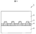
- FIG. 1 is a vertical sectional view of a semiconductor multilayer structure (first embodiment).
- Figure 2 is a conceptual diagram showing the orientation relationship between the ⁇ -Ga 2 O 3 and the unit cell of the crystal, ⁇ -Ga 2 O 3 principal surface of the substrate (the first embodiment).
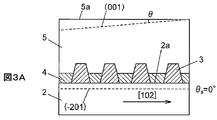
- FIG. 3A is a schematic diagram showing the relationship between the offset angle ⁇ s of the main surface of the Ga 2 O 3 substrate and the inclination angle ⁇ of the main surface of the nitride semiconductor layer (first embodiment).
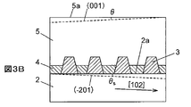
- FIG. 3B is a schematic diagram showing the relationship between the offset angle ⁇ s of the main surface of the Ga 2 O 3 substrate and the inclination angle ⁇ of the main surface of the nitride semiconductor layer (first embodiment).
- FIG. 3A is a schematic diagram showing the relationship between the offset angle ⁇ s of the main surface of the Ga 2 O 3 substrate and the inclination angle ⁇ of the main surface of the nitride semiconductor layer (first embodiment).
- FIG. 3B is a schematic diagram showing the
- FIG. 3C is a schematic diagram illustrating a relationship between an offset angle ⁇ s of the main surface of the Ga 2 O 3 substrate and an inclination angle ⁇ of the main surface of the nitride semiconductor layer (first embodiment).
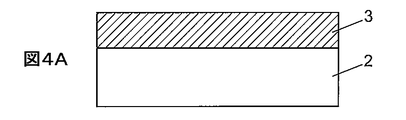
- FIG. 4A is a vertical cross-sectional view illustrating a manufacturing process of a semiconductor stacked structure (first embodiment).
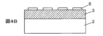
- FIG. 4B is a vertical cross-sectional view illustrating the manufacturing process of the semiconductor stacked structure (first embodiment).
- FIG. 4C is a vertical cross-sectional view illustrating the manufacturing process of the semiconductor stacked structure (first embodiment).
- FIG. 4D is a vertical cross-sectional view illustrating the manufacturing process of the semiconductor stacked structure (first embodiment).
- FIG. 4E is a vertical cross-sectional view illustrating the manufacturing process of the semiconductor stacked structure (first embodiment).
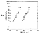
- FIG. 5A is a graph showing variation in crystal quality of a nitride semiconductor layer for each semiconductor stacked structure (first embodiment).
- FIG. 5B is a graph showing variation in crystal quality of the nitride semiconductor layer for each semiconductor stacked structure (first embodiment).
- FIG. 6 is a graph showing variations in dislocation density for each semiconductor stacked structure (first embodiment).
- FIG. 7 is a vertical sectional view of a semiconductor laminated structure in which electrodes for measuring current-voltage characteristics are connected (first embodiment).
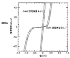
- FIG. 8A is a graph showing the current density-voltage characteristic in the vertical direction of the semiconductor multilayer structure (first embodiment).
- FIG. 8B is a graph showing the current density-voltage characteristics in the vertical direction of the semiconductor stacked structure (first embodiment).
- FIG. 9 is a graph showing an example of the relationship between the material of the dielectric layer and the light extraction efficiency of the light emitting element obtained by optical simulation (first embodiment).
- FIG. 10A is a graph showing variation in crystal quality of a nitride semiconductor layer for each semiconductor stacked structure (first embodiment).
- FIG. 10B is a graph showing variation in crystal quality of the nitride semiconductor layer for each semiconductor stacked structure (first embodiment).
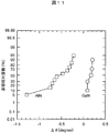
- FIG. 11 is a graph showing variation in ⁇ for each semiconductor stacked structure (first embodiment).
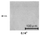
- FIG. 12A is a photograph showing the state of the main surface of the nitride semiconductor layer when the inclination angle ⁇ of the main surface of the nitride semiconductor layer is 0.14 ° (first embodiment).
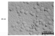
- FIG. 12B is a photograph showing the state of the main surface of the nitride semiconductor layer when the inclination angle ⁇ of the main surface of the nitride semiconductor layer is 0.25 ° (first embodiment).
- FIG. 12C is a photograph showing the state of the main surface of the nitride semiconductor layer when the inclination angle ⁇ of the main surface of the nitride semiconductor layer is 0.45 ° (first embodiment).
- FIG. 12A is a photograph showing the state of the main surface of the nitride semiconductor layer when the inclination angle ⁇ of the main surface of the nitride semiconductor layer is 0.14 ° (first embodiment).
- FIG. 12B is a photograph showing the state of the main surface of the nitride semiconductor layer when the inclination angle
- FIG. 12D is a photograph showing the state of the main surface of the nitride semiconductor layer when the inclination angle ⁇ of the main surface of the nitride semiconductor layer is 0.63 ° (first embodiment).
- FIG. 13A is a photograph showing the state of the main surface of a nitride semiconductor layer when a GaN buffer layer is used (first embodiment).
- FIG. 13B is a photograph showing the state of the main surface of the nitride semiconductor layer when an AlN buffer layer is used (first embodiment).
- FIG. 14 is a vertical sectional view of a vertical LED (second embodiment).
- FIG. 15 is a vertical sectional view of a vertical FET (third embodiment).
- FIG. 16 is a vertical sectional view of a vertical FET (fourth embodiment).
- FIG. 17 is a vertical sectional view of a vertical FET (fifth embodiment).
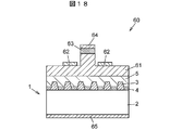
- FIG. 18 is a vertical sectional view of a vertical FET (sixth embodiment).
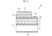
- FIG. 19 is a vertical sectional view of an HBT (seventh embodiment).
- FIG. 20 is a vertical sectional view of an SBD (eighth embodiment).
- the Ga 2 O 3 substrate 2 is made of ⁇ -Ga 2 O 3 single crystal.
- the upper surface of the Ga 2 O 3 substrate 2 is a flat surface without unevenness, and can serve as a foundation for the growth of high-quality nitride semiconductor crystals (101), ( ⁇ 201), (310), (3 A plane having a plane orientation of ⁇ 10), (100), etc.
- the refractive index of the Ga 2 O 3 substrate 2 is approximately 1.9.
- FIG. 2 is a conceptual diagram showing the orientation relationship between the unit cell of ⁇ -Ga 2 O 3 crystal and the main surface 2 a of the ⁇ -Ga 2 O 3 substrate 2.
- ⁇ s represents an offset angle in the [102] direction from the ( ⁇ 201) plane.
- the offset angle from the ( ⁇ 201) plane in the [010] direction is 0 °.
- a unit cell 2b in FIG. 2 is a unit cell of ⁇ -Ga 2 O 3 crystal.
- a 0 , b 0 , and c 0 represent axis lengths in the [100] direction, [010] direction, and [001] direction, respectively.
- the main surface 2a of the Ga 2 O 3 substrate 2 is a surface inclined with an offset angle ⁇ s in the [102] direction with respect to the ( ⁇ 201) plane, ie, the normal vector is based on the normal vector of the ( ⁇ 201) plane.
- the surface is inclined at an offset angle ⁇ s in the [102] direction.
- the offset angle ⁇ s is preferably ⁇ 0.4 ° or more and 0.2 ° or less, and more preferably ⁇ 0.2 ° or more and 0.0 ° or less.
- the dielectric layer 3 is made of, for example, a SiN layer containing SiN as a main component, and has a refractive index difference of 0.15 or less with respect to the Ga 2 O 3 substrate 2.
- the refractive index of the Ga 2 O 3 substrate 2 is 1.9, for example, the refractive index of the dielectric layer 3 is 1.75 or more and 2.05 or less.
- the pattern shape of the dielectric layer 3 is, for example, a mesa pattern, a recess pattern, a line and space pattern, or the like.
- Refractive index of the dielectric layer 3 is closer to the refractive index of the Ga 2 O 3 substrate 2, to suppress the total reflection at the interface of Ga 2 O 3 substrate 2 and the dielectric layer 3, the efficiency of the light from the light-emitting layer Can be taken out.
- the dielectric layer 3 is a SiN layer, elements other than Si and N such as O may be included for adjusting the refractive index.
- the refractive index of the dielectric layer 3 is adjusted by controlling the formation conditions such as the film formation temperature of the dielectric layer 3, and the difference between the refractive index of the dielectric layer 3 and the refractive index of the Ga 2 O 3 substrate 2 is adjusted. Can be made smaller.
- the GaN buffer layer 4 is made of a GaN crystal and may contain a conductivity type impurity such as Si.
- the nitride semiconductor layer 5 Crystal quality can be increased.
- the nitride semiconductor layer 5 may have a multilayer structure in which a plurality of layers made of different nitride semiconductor crystals are stacked.
- the light emitting layer and the clad layer sandwiching the light emitting layer can be constituted by the nitride semiconductor layer 5.
- the Ga 2 O 3 substrate 2 and the nitride semiconductor layer 5 may include a conductive impurity such as Si or Sn.
- FIG. 3A to 3C are schematic diagrams showing the relationship between the offset angle ⁇ s of the main surface 2a of the Ga 2 O 3 substrate 2 and the inclination angle ⁇ of the main surface 5a of the nitride semiconductor layer 5.
- FIG. 3A to 3C are planes parallel to the [102] direction, which are orthogonal to the ( ⁇ 201) plane of the Ga 2 O 3 substrate 2.
- the main surface 5a of the nitride semiconductor layer 5 has a predetermined inclination angle ⁇ . Tilted from the (001) plane.
- the inclination angle ⁇ of the main surface 5a of the nitride semiconductor layer 5 is made closer to 0 ° by providing the main surface 2a of the Ga 2 O 3 substrate 2 with an appropriate offset angle ⁇ s. Can do. Thereby, the surface roughness of main surface 5a of nitride semiconductor layer 5 can be effectively reduced.
- the inclination angle ⁇ of the main surface 5a of the nitride semiconductor layer 5 is set to 0.
- the offset angle ⁇ s of the main surface 2a of the Ga 2 O 3 substrate 2 is ⁇ 0.2 ° or more and 0.0 ° or less.
- the inclination angle ⁇ of the main surface 5a of the nitride semiconductor layer 5 can be within a numerical range of ⁇ 0.2 ° to 0.2 ° which is closer to 0 °.
- 4A to 4E are vertical cross-sectional views showing the manufacturing process of the semiconductor multilayer structure according to the first embodiment.
- organic cleaning and SPM (Sulfuric acid / hydrogen peroxide mixture) cleaning are performed on the Ga 2 O 3 substrate 2 subjected to CMP (Chemical Mechanical Polishing).
- the Ga 2 O 3 substrate 2 is transferred into the chamber of the plasma CVD apparatus.
- a film-like dielectric layer 3 is formed on the Ga 2 O 3 substrate 2.
- This film-like dielectric layer 3 is made of SiH 4 as a raw material of Si, NH 3 gas as a raw material of N, and N 2 gas as an atmospheric gas while maintaining the temperature in the chamber at 300 to 350 ° C. Is supplied into the chamber, and SiN is deposited on the Ga 2 O 3 substrate 2.
- the dielectric layer 3 is a substantially uniform film having a thickness of about 1 ⁇ m.
- the raw materials for each element are not limited to the above.
- a resist pattern 6 is formed on the dielectric layer 3.
- the pattern shape of the resist pattern 6 is, for example, a triangular lattice pattern with a dot diameter of 2 ⁇ m and a pitch of 4 ⁇ m.
- the resist pattern 6 is formed by, for example, photolithography.
- the dielectric layer 3 is etched with BHF (buffered hydrofluoric acid) using the resist pattern 6 as a mask, and the pattern of the resist pattern 6 is transferred to the dielectric layer 3.
- BHF buffered hydrofluoric acid
- the remaining resist pattern 6 is removed.
- the surface of the structure composed of the Ga 2 O 3 substrate 2 and the dielectric layer 3 is cleaned by organic cleaning and SPM cleaning, and transported to the MOCVD apparatus.
- GaN buffer layer 4 is formed by maintaining NH 3 as a raw material for N, trimethyl gallium (TMG) as a raw material for Ga, and maintaining the substrate surface temperature at around 500 ° C.
- TMG trimethyl gallium
- NH 3 gas as a raw material for N trimethylgallium (TMG) gas as a raw material for Ga
- trimethylaluminum (TMA) gas as a raw material for Al trimethylindium (TMI) gas as a raw material for In are contained in the chamber.
- the Al x Ga y In z N crystal which is a nitride semiconductor crystal, is selectively grown on the Ga 2 O 3 substrate 2 to form the nitride semiconductor layer 5. Thereby, the semiconductor multilayer structure 1 is obtained.
- the nitride semiconductor crystal constituting the nitride semiconductor layer 5 grows from a region not covered by the dielectric layer 3 on the upper surface of the Ga 2 O 3 substrate 2 and does not grow from the dielectric layer 3.
- the nitride semiconductor crystal grows selectively, and then grows in the lateral direction to cover the dielectric layer 3.
- the dislocation density in the nitride semiconductor layer 5 is reduced, and the crystal quality is improved.
- Such a crystal growth method using selective growth is called ELO (Epitaxial Lateral Overgrowth).
- (Crystal quality) 5A and 5B are graphs showing variations in crystal quality of the nitride semiconductor layer 5 for each semiconductor stacked structure 1.
- 5A shows the cumulative relative power distribution of the half width of the X-ray rocking curve in the (002) plane diffraction of the nitride semiconductor layer 5
- FIG. 5B shows the X-ray rocking curve in the (101) plane diffraction of the nitride semiconductor layer 5.
- the marks ⁇ plotted in FIGS. 5A and 5B represent the cumulative relative frequency distribution of the full width at half maximum of the X-ray rocking curve in the semiconductor multilayer structure 1 using the GaN buffer layer 4, and the marks ⁇ used the AlN buffer layer.
- the cumulative relative frequency distribution of the half value width of the X-ray rocking curve in a semiconductor lamination structure is expressed.
- 5A and 5B show that, when the GaN buffer layer 4 is used, the variation in the crystal quality of the nitride semiconductor layer 5 for each semiconductor stacked structure 1 does not change much as compared with the case where the AlN buffer layer is used. It shows that the crystal quality of the physical semiconductor layer 5 is improved.
- the half width was 223 to 269 arcsec in (002) plane diffraction and 225 to 264 arcsec in (101) plane diffraction.
- FIG. 6 is a graph showing variation in dislocation density for each semiconductor stacked structure.
- the mark ⁇ plotted in FIG. 6 represents the cumulative relative frequency distribution of the dislocation density of the X-ray rocking curve in the semiconductor multilayer structure 1 using the GaN buffer layer 4, and the mark ⁇ represents the semiconductor multilayer using the AlN buffer layer. It represents the cumulative relative frequency distribution of the dislocation density of the structure.
- the dislocation density was evaluated by using cathodoluminescence and counting the density of dark spots.
- the dislocation density evaluation results can also be obtained by counting the density of etch pits obtained by TEM observation or chemical etching using KOH, NaOH, or the like.
- FIG. 6 shows that in both the measurement results for the GaN buffer layer 4 and the AlN buffer layer, the crystal quality of the nitride semiconductor layer 5 varies from one semiconductor stack structure 1 to another and the dislocation density is almost the same. This value is comparable to that on the sapphire substrate, indicating that the crystal quality of the nitride semiconductor layer 5 is high.
- the dislocation density when using the GaN buffer layer 4 was 1.52 ⁇ 10 8 to 2.14 ⁇ 10 8 / cm 2 .
- FIG. 7 shows a state in which electrodes are connected to the Ga 2 O 3 substrate 2 and the nitride semiconductor layer 5 of the semiconductor multilayer structure 1.
- FIG. 8A and 8B are graphs showing the current density-voltage characteristics in the vertical direction of the semiconductor multilayer structure 1.
- the horizontal axis represents voltage (V)
- the vertical axis represents current density (A / cm 2 ).
- FIG. 8A shows the current density-voltage characteristic when the GaN buffer layer 4 is used
- FIG. 8B shows the current density-voltage characteristic when the AlN buffer layer is used.
- the plotted mark ⁇ represents the current density-voltage characteristic in the vertical direction of the semiconductor multilayer structure 1 without the dielectric layer 3, and the mark ⁇ represents the semiconductor multilayer structure with the dielectric layer. Represents the current density-voltage characteristics in the vertical direction.
- the dielectric layer 3 is a SiN layer, it has been confirmed that the current density-voltage characteristics in the vertical direction (vertical direction) of the semiconductor multilayer structure 1 can be obtained particularly excellent.
- the semiconductor laminated structure having the dielectric layer 3 that is the SiN layer is used to cause a specific current to flow more than the semiconductor laminated structure that does not have the dielectric layer that is the SiN layer.
- the required voltage is small. This result indicates that the drive voltage can be reduced by providing the dielectric layer 3 which is a SiN layer.
- FIG. 9 is a graph showing an example of the relationship between the material of the dielectric layer 3 and the light extraction efficiency of the light emitting element obtained by optical simulation.
- the Ga 2 O 3 substrate 2 has a refractive index of 1.9
- the dielectric layer 3 is composed of a mesa pattern having a diameter of 3 ⁇ m, a pitch of 6 ⁇ m, and a height of 1 ⁇ m, and light emitted from the light emitting layer.
- the light extraction efficiency in FIG. 9 is standardized on the basis of the light extraction efficiency in the case where unevenness of the same shape is formed on the surface of the Ga 2 O 3 substrate 2 instead of the dielectric layer in the light emitting element.
- this standard light extraction efficiency is that an n-type cladding layer, a light-emitting layer, a p-type cladding layer, and a contact layer with good crystal quality are formed on the Ga 2 O 3 substrate 2 having irregularities formed on the surface. This is the theoretical value when assumed.
- FIG. 9 shows that when the SiN layer that satisfies the refractive index condition of the dielectric layer is used as the dielectric layer 3, the light extraction efficiency is the highest.
- the light extraction efficiency is about 98.5% or more of the reference value.
- FIG. 10A and 10B are graphs showing an in-plane distribution of the difference ⁇ between the offset angle ⁇ s of the main surface of the Ga 2 O 3 substrate 2 and the inclination angle ⁇ of the main surface of the nitride semiconductor layer 5. It is.
- FIG. 10A shows the distribution of ⁇ when the GaN buffer layer 4 is used
- FIG. 10B shows the distribution of ⁇ when the AlN buffer layer is used.
- the horizontal axis in FIGS. 10A and 10B represents the position in the X direction or Y direction in the plane of the semiconductor multilayer structure 1.
- the mark ⁇ plotted in FIGS. 10A and 10B represents a measured value on a line parallel to the [010] direction of the Ga 2 O 3 substrate 2 through the center in the plane of the semiconductor multilayer structure 1.
- the mark ⁇ represents a measured value on a line parallel to the [102] direction of the Ga 2 O 3 substrate 2 through the center in the plane of the semiconductor multilayer structure 1.
- the variation in ⁇ in the plane of the semiconductor multilayer structure 1 is smaller in both the [010] direction and the [102] direction when the AlN buffer layer is used.
- the difference between the maximum value and the minimum value of ⁇ in the plane was 0.15 ° in the [010] direction and 0.07 ° in the [102] direction.
- FIG. 11 is a graph showing variation in ⁇ in the [102] direction of the Ga 2 O 3 substrate 2 for each semiconductor multilayer structure 1.
- the vertical axis represents the cumulative relative frequency distribution of ⁇ .
- 11 represents the cumulative relative power distribution of ⁇ in the semiconductor multilayer structure 1 using the GaN buffer layer 4, and the mark ⁇ represents the cumulative ⁇ in the semiconductor multilayer structure using the AlN buffer layer. Represents a relative frequency distribution. Note that these values of ⁇ are measured at the center position in the plane.
- FIG. 11 shows that when the GaN buffer layer 4 is used, the variation in ⁇ for each semiconductor multilayer structure 1 is smaller than when the AlN buffer layer is used.
- the difference between the maximum value and the minimum value of ⁇ between the semiconductor stacked structures when the GaN buffer layer 4 was used was 0.12 °.
- the inclination angle ⁇ of the main surface of the nitride semiconductor layer 5 in the [102] direction of the Ga 2 O 3 substrate 2 is 0.14 °, 0.25 °, 0.45 °, 0.63 °. 6 is a photograph showing the state of the main surface of nitride semiconductor layer 5 when.
- step bunching appearing on the main surface of the nitride semiconductor layer 5 increases as the tilt angle ⁇ increases.
- Step bunching is hardly confirmed on the main surface of the nitride semiconductor layer 5 shown in FIGS. 12A and 12B, but step bunching is clearly confirmed on the main surface of the nitride semiconductor layer 5 shown in FIGS. 12C and 12D. it can.
- the step bunching can be clearly confirmed when the inclination angle ⁇ is larger than approximately 0.4 ° (smaller than ⁇ 0.4 °). Further, when the inclination angle ⁇ is approximately ⁇ 0.2 ° or more and 0.2 ° or less, it is presumed that the step bunching becomes smaller and the smooth surface is obtained as the observation with the optical microscope becomes difficult.
- FIG. 13A is a photograph showing the state of the main surface of the nitride semiconductor layer 5 when the GaN buffer layer 4 is used
- FIG. 13B is a photograph of the main surface of the nitride semiconductor layer when the AlN buffer layer is used. It is a photograph showing the state.
- FIGS. 13A and 13B when the GaN buffer layer 4 is used, the hillock-like convex portions observed on the main surface of the nitride semiconductor layer 5 are greatly reduced as compared with the case where the AlN buffer layer is used. Is shown.
- the hillock density of the main surface of the nitride semiconductor layer 5 is less than 1 per 1 cm 2 when the GaN buffer layer 4 is used, and 10 2 to 10 3 per 1 cm 2 when the AlN buffer layer is used. It was a piece.
- the generation of hillocks is hardly affected by the inclination angle ⁇ of the main surface of the nitride semiconductor layer 5, but the surface flatness is improved more effectively by reducing the hillock density using the GaN buffer layer 4. can do.
- the semiconductor multilayer structure 1 according to the first embodiment can be used for manufacturing various semiconductor elements. Below, vertical LED is demonstrated as an example of the semiconductor element.
- FIG. 14 is a vertical sectional view of the vertical LED 10 according to the second embodiment.
- the vertical LED 10 includes a Ga 2 O 3 substrate 2, a dielectric layer 3 and a GaN buffer layer 4 on the Ga 2 O 3 substrate 2, an n-type cladding layer 14 on the GaN buffer layer 4, and an n-type cladding layer 14.
- the upper light emitting layer 15, the p-type cladding layer 16 on the light-emitting layer 15, the contact layer 17 on the p-type cladding layer 16, the p-type electrode 18 on the contact layer 17, and the GaN of the Ga 2 O 3 substrate 2 It has an n-type electrode 19 on the surface opposite to the buffer layer 4.
- the side surface of the laminate composed of the dielectric layer 3, the GaN buffer layer 4, the n-type cladding layer 14, the light emitting layer 15, the p-type cladding layer 16, and the contact layer 17 is covered with the insulating film 20.
- the n-type cladding layer 14 corresponds to the nitride semiconductor layer 5 constituting the semiconductor multilayer structure 1 of the first embodiment.
- the thicknesses of the Ga 2 O 3 substrate 2, the dielectric layer 3, the GaN buffer layer 4, and the n-type cladding layer 14 are, for example, 400 ⁇ m, 1 ⁇ m, 48 nm, and 5 ⁇ m.
- the light emitting layer 15 is composed of, for example, a three-layered multiple quantum well structure and a GaN crystal film having a thickness of 10 nm thereon.
- Each multiple quantum well structure is composed of a GaN crystal film having a thickness of 6 nm and an InGaN crystal film having a thickness of 2 nm.
- the light emitting layer 15 is formed by epitaxially growing each crystal film on the n-type cladding layer 14 at a growth temperature of 700 to 800 ° C., for example.
- the p-type cladding layer 16 is, for example, a GaN crystal film having a thickness of 100 nm and containing Mg having a concentration of 5.0 ⁇ 10 19 / cm 3 .
- the p-type cladding layer 16 is formed, for example, by epitaxially growing a GaN crystal containing Mg on the light emitting layer 15 at a growth temperature of 900 to 1050 ° C.
- the contact layer 17 is, for example, a GaN crystal film having a thickness of 10 nm and containing Mg having a concentration of 1.5 ⁇ 10 20 / cm 3 .
- the contact layer 17 is formed, for example, by epitaxially growing a GaN crystal containing Mg on the p-type cladding layer 16 at a growth temperature of 900 to 1050 ° C.
- the n-type cladding layer 14, the light emitting layer 15, the p-type cladding layer 16, and the contact layer 17 TMG (trimethylgallium) gas as the Ga material, TMI (trimethylindium) gas as the In material, MtSiH 3 (monomethylsilane) gas can be used as the Si material, Cp 2 Mg (biscyclopentadienylmagnesium) gas can be used as the Mg material, and NH 3 (ammonia) gas can be used as the N material.
- TMG trimethylgallium
- TMI trimethylindium
- MtSiH 3 (monomethylsilane) gas can be used as the Si material
- Cp 2 Mg (biscyclopentadienylmagnesium) gas can be used as the Mg material
- NH 3 (ammonia) gas can be used as the N material.
- the insulating film 20 is made of an insulating material made of SiO 2 or the like, and is formed, for example, by sputtering.
- the p-type electrode 18 and the n-type electrode 19 are electrodes that are in ohmic contact with the contact layer 17 and the Ga 2 O 3 substrate 2, respectively, and are formed by, for example, a vapor deposition apparatus.
- the vertical LED 10 includes a dielectric layer 3, a GaN buffer layer 4, an n-type cladding layer 14, a light-emitting layer 15, a p-type cladding layer 16, a contact layer 17, and a p-type electrode on a Ga 2 O 3 substrate 2 in a wafer state. After the 18 and n-type electrodes 19 are formed, they are obtained by dicing them into, for example, a 300 ⁇ m square chip size.
- the vertical LED 10 is, for example, an LED chip that extracts light from the Ga 2 O 3 substrate 2 side, and is mounted on a can-type stem using Ag paste.
- the n-type cladding layer 14 of the vertical LED 10 is formed on the Ga 2 O 3 substrate 2 whose main surface is a surface inclined at a special offset angle, the surface roughness is small and the crystal quality is excellent. .
- the light emitting layer 15, the p-type cladding layer 16, and the contact layer 17 formed by epitaxial crystal growth on the n-type cladding layer 14 having excellent crystal quality also have excellent crystal quality. For this reason, the LED element 10 is excellent in leak characteristics and reliability.
- a dielectric layer structure made of SiN or the like is provided on a ⁇ -Ga 2 O 3 substrate whose principal surface is a plane inclined from the ( ⁇ 201) plane, and a buffer layer made of GaN crystals is provided.
- hillocks with a narrow half-value width by X-ray rocking curve measurement low dislocation density, excellent electrical conductivity, excellent light extraction efficiency, small off-angle variation in the surface, and poor surface morphology.
- the density of can be reduced.
- the off-angle variation between wafers is small, and a nitride semiconductor layer with stable quality can be obtained.
- nitride semiconductor layer By using such a nitride semiconductor layer, it is possible to produce a semiconductor device excellent in overall device characteristics determined by leakage current, reliability, temperature characteristics, light emission efficiency, and the like with a high yield.
- FIG. 15 is a vertical sectional view of a vertical FET which is a semiconductor element according to the third embodiment.
- the vertical FET 30 includes a semiconductor laminated structure 1 including a Ga 2 O 3 substrate 2, a dielectric layer 3, a GaN buffer layer 4, and a nitride semiconductor layer (n + -GaN layer) 5, and a nitride semiconductor layer 5.
- a GaN-based vertical FET 31 formed on the surface (the upper surface in FIG. 15), a gate electrode 32 and a source electrode 33 formed on the GaN-based vertical FET 31, and the surface of the Ga 2 O 3 substrate 2 (FIG. 15 and the drain electrode 34 formed on the lower surface in FIG.
- the vertical FET 30 is an example of a vertical FET that can be formed using the semiconductor multilayer structure 1.
- FIG. 16 is a vertical sectional view of a vertical FET which is a semiconductor element according to the fourth embodiment.
- the vertical FET 40 includes a semiconductor laminated structure 1 including a Ga 2 O 3 substrate 2, a dielectric layer 3, a GaN buffer layer 4, and a nitride semiconductor layer (n + -GaN layer) 5, and a nitride semiconductor layer 5.
- a semiconductor laminated structure 1 including a Ga 2 O 3 substrate 2, a dielectric layer 3, a GaN buffer layer 4, and a nitride semiconductor layer (n + -GaN layer) 5, and a nitride semiconductor layer 5.
- the p + -GaN layer 41 formed by introducing a p-type impurity, Al 0.2 Ga 0.8 N layer formed on the surface of the nitride semiconductor layer 5 (the upper surface in FIG.
- a Si ion implanted region 43 formed by introducing n-type impurities such as Si into the Al 0.2 Ga 0.8 n layer 42, on the Al 0.2 Ga 0.8 n layer 42
- the gate electrode 45 formed through the gate insulating film 44, the source electrode 46 connected to the Si ion implantation region 43 and the p + -GaN layer 41, and the surface of the Ga 2 O 3 substrate 2 (the lower side in FIG. 16)
- the drain electrode 4 formed on the surface Including the door.
- the thickness of the nitride semiconductor layer 5 is, for example, 5 ⁇ m, and the Si concentration is 1 ⁇ 10 18 / cm 3 .
- the thickness of the p + -GaN layer 41 is, for example, 1 ⁇ m, and the concentration of the p-type impurity is 1 ⁇ 10 18 / cm 3 .
- the Al 0.2 Ga 0.8 N layer 42 does not contain impurities and has a thickness of, for example, 30 nm.
- the source electrode 46 is made of a laminate of, for example, a Ti film and an Al film.
- the drain electrode 47 is made of a laminate of, for example, a Ti film and an Au film.
- the gate electrode 45 is made of, for example, Al, and the gate insulating film 44 is made of, for example, SiO 2 .
- the vertical FET 40 is an example of a vertical FET having a MIS gate structure that can be formed using the semiconductor multilayer structure 1.
- FIG. 17 is a vertical sectional view of a vertical FET which is a semiconductor element according to the fifth embodiment.
- the vertical FET 50 includes a semiconductor multilayer structure 1 including a Ga 2 O 3 substrate 2, a dielectric layer 3, a GaN buffer layer 4, and a nitride semiconductor layer (n ⁇ -GaN layer) 5, and a nitride semiconductor layer 5.
- a gate electrode 55 formed on the Ga 0.8 n layer 54 is connected to the p + -GaN layer 51, n + -GaN layer 52, GaN layer 53, and Al 0.2 Ga 0.8 n layer 54
- the thickness of the nitride semiconductor layer 5 is, for example, 5 ⁇ m, and the Si concentration is 1 ⁇ 10 16 / cm 3 .
- the thickness of the p + -GaN layer 51 is, for example, 1 ⁇ m, and the concentration of the p-type impurity is 1 ⁇ 10 18 / cm 3 .
- the thickness of the n + -GaN layer 52 is, for example, 200 nm, and the concentration of the n-type impurity is 1 ⁇ 10 18 / cm 3 .
- the GaN layer 53 does not contain impurities and has a thickness of, for example, 100 nm.
- the Al 0.2 Ga 0.8 N layer 54 does not contain impurities and has a thickness of, for example, 30 nm.
- the source electrode 56 is made of a laminate of, for example, a Ti film and an Al film.
- the drain electrode 57 is made of a laminate of, for example, a Ti film and an Au film.
- the gate electrode 55 is made of, for example, a stacked body of a Ni film and an Au film.
- the vertical FET 50 is an example of a vertical FET having a Schottky gate structure that can be formed using the semiconductor multilayer structure 1.
- FIG. 18 is a vertical sectional view of a vertical FET which is a semiconductor element according to the sixth embodiment.
- the vertical FET 60 includes a semiconductor multilayer structure 1 including a Ga 2 O 3 substrate 2, a dielectric layer 3, a GaN buffer layer 4, and a nitride semiconductor layer (n + -GaN layer) 5, and a nitride semiconductor layer 5. surface n formed (upper surface in FIG.
- the thickness of the nitride semiconductor layer 5 is, for example, 5 ⁇ m, and the Si concentration is 1 ⁇ 10 18 / cm 3 .
- the thickness of the flat portion of the n ⁇ -GaN layer 61 is, for example, 3 ⁇ m, and the concentration of the n-type impurity is 1 ⁇ 10 16 / cm 3 .
- the source electrode 64 is made of, for example, WSi.
- the drain electrode 65 is made of a laminate of, for example, a Ti film and an Al film.
- the gate electrode 62 is made of, for example, PdSi.
- the vertical FET 60 is an example of a vertical FET having a Schottky gate structure that can be formed using the semiconductor multilayer structure 1.
- HBT heterojunction bipolar transistor
- FIG. 19 is a vertical sectional view of an HBT that is a semiconductor element according to the seventh embodiment.
- the HBT 70 includes a semiconductor multilayer structure 1 including a Ga 2 O 3 substrate 2, a dielectric layer 3, a GaN buffer layer 4, and a nitride semiconductor layer (n + -GaN layer) 5, and the surface of the nitride semiconductor layer 5 ( The n ⁇ -GaN layer 71 and the p + -GaN layer 72 stacked on the upper surface in FIG. 19 and the n + —Al 0.1 Ga 0.9 N stacked on the p + -GaN layer 72.
- the thickness of the nitride semiconductor layer 5 is, for example, 4 ⁇ m, and the Si concentration is 1 ⁇ 10 18 / cm 3 .
- the thickness of the n ⁇ -GaN layer 71 is, for example, 2 ⁇ m, and the concentration of the n-type impurity is 1 ⁇ 10 16 / cm 3 .
- the thickness of the p + -GaN layer 72 is, for example, 100 nm, and the concentration of the p-type impurity is 1 ⁇ 10 18 / cm 3 .
- the thickness of the n + -Al 0.1 Ga 0.9 N layer 73 is, for example, 500 nm, and the concentration of n-type impurities is 1 ⁇ 10 18 / cm 3 . Further, the thickness of the n + -GaN layer 74 is, for example, 1 ⁇ m, and the concentration of the n-type impurity is 1 ⁇ 10 18 / cm 3 .
- the emitter electrode 77 is made of a laminate of, for example, a Ti film and an Al film.
- the collector electrode 76 is made of a laminated body of, for example, a Ti film and an Au film.
- the base electrode 75 is made of, for example, a laminate of Ni film and Au film.
- the HBT 70 is an example of a heterojunction bipolar transistor that can be formed using the semiconductor multilayer structure 1.
- FIG. 20 is a cross-sectional view of an SBD that is a semiconductor element according to the eighth embodiment.
- the SBD 80 includes a semiconductor laminated structure 1 including a Ga 2 O 3 substrate 2, a dielectric layer 3, a GaN buffer layer 4, and a nitride semiconductor layer (n + -GaN layer) 5, and a surface of the nitride semiconductor layer 5 ( The n ⁇ -GaN layer 81 formed on the upper surface in FIG. 20, the anode electrode 82 formed on the n ⁇ -GaN layer 81, and the surface of the Ga 2 O 3 substrate 2 (lower side in FIG. 20). A cathode electrode 83 formed on the surface.
- the thickness of the nitride semiconductor layer 5 is, for example, 5 ⁇ m, and the Si concentration is 1 ⁇ 10 18 / cm 3 .
- the thickness of the n ⁇ -GaN layer 81 is, for example, 7 ⁇ m, and the concentration of the n-type impurity is 1 ⁇ 10 16 / cm 3 .
- the anode electrode 82 is made of, for example, Au.
- the cathode electrode 83 is made of, for example, a laminate of a Ti film and an Au film.
- the SBD 80 is an example of a Schottky barrier diode that can be formed using the semiconductor multilayer structure 1.
- a high-quality nitride semiconductor layer can be obtained.
- the half width by X-ray rocking curve measurement is narrow, the dislocation density is low, the electric conduction characteristics are excellent, the off-angle variation in the surface is small, and the density of hillocks, which are surface morphology defects, can be reduced.
- the off-angle variation between wafers is small, and a nitride semiconductor layer with stable quality can be obtained. Further, by using such a semiconductor multilayer structure, device characteristics such as reliability, leakage current, and temperature characteristics can be improved comprehensively.
- a semiconductor laminated structure having a nitride semiconductor layer with high quality and high uniformity in the surface capable of comprehensively improving device characteristics determined by reliability, leakage current, temperature characteristics, luminous efficiency, etc., And a semiconductor device including the semiconductor multilayer structure.
Landscapes
- Led Devices (AREA)
- Electrodes Of Semiconductors (AREA)
- Bipolar Transistors (AREA)
- Junction Field-Effect Transistors (AREA)
Abstract
酸化ガリウム基板上の品質が高く、かつ面内において均一性の高い窒化物半導体層を有する半導体積層構造体、及びその半導体積層構造体を含む半導体素子を提供する。 半導体積層構造体1は、Ga2O3基板2と、Ga2O3基板2の上面に部分的に接触するように形成され、Ga2O3基板2との屈折率の差が0.15以下である誘電体層3と、Ga2O3基板2の誘電体層4に覆われていない残りの上面に接触するように形成されたGaN結晶からなるバッファ層4と、Ga2O3基板2上にバッファ層4を介して形成されたAlxGayInzN(0≦x≦1、0≦y≦1、0≦z≦1、x+y+z=1)結晶からなる窒化物半導体層5とを有する。
Description
本発明は、半導体積層構造体及び半導体素子に関する。
従来の発光素子として、透光性基板の凹凸パターンが形成された面の上に結晶膜を成長させることにより形成されるものが知られている(例えば、特許文献1参照)。特許文献1においては、サファイア基板の凹凸パターンが形成された面上にGaN系半導体層を成長させる。
上記特許文献1のサファイア基板の凹凸パターンは、サファイア基板とGaN系半導体層との界面における、サファイア基板とGaN系半導体層との屈折率の違いに起因するGaN系半導体層中の発光層から発せられた光の反射を抑える機能を有する。このような反射を抑えることにより、発光層による反射光の吸収や、反射光の多重反射による減衰を低減し、発光素子の光取出効率を向上させることができる。
しかしながら、単斜晶系に属するβ-ガリア構造を有したβ‐Ga2O3単結晶基板では、基板加工の方向によっては、加工部側壁等からもGaN系半導体層が成長してしまうことにより、基板垂直方向にc軸を有した結晶と垂直方向以外にc軸を有した結晶が混在し、GaN系半導体層は多結晶となる恐れがある。その場合には、窒化物半導体層の品質が著しく悪くなることが、本発明者等によって明らかにされている(例えば、特許文献2参照)。
本発明は、このような事情を鑑みてなされたものであり、本発明の目的は、酸化ガリウム基板上の品質が高く、かつ面内において均一性の高い窒化物半導体層を有する半導体積層構造体、及びその半導体積層構造体を含む半導体素子を提供することにある。
本発明の一態様は、上記目的を達成するために、[1]~[5]の半導体積層構造体を提供する。
[1]Ga2O3基板と、前記Ga2O3基板の上面に部分的に接触するように形成され、前記Ga2O3基板との屈折率の差が0.15以下である誘電体層と、前記Ga2O3基板の前記誘電体層に覆われていない残りの上面に接触するように形成されたGaN結晶からなるバッファ層と、前記Ga2O3基板上に前記バッファ層を介して形成されたAlxGayInzN(0≦x≦1、0≦y≦1、0≦z≦1、x+y+z=1)結晶からなる窒化物半導体層と、を有する半導体積層構造体。
[2]前記窒化物半導体層は、X線ロッキングカーブ測定において(002)面回折の半値幅が270秒以下である[1]に記載の半導体積層構造体。
[3]前記窒化物半導体層は、X線ロッキングカーブ測定において(101)面回折の半値幅が270秒以下である[1]又は[2]に記載の半導体積層構造体。
[4]前記誘電体層は、SiNを主成分とするSiN層からなる[1]~[3]のいずれか1項に記載の半導体積層構造体。
[5]前記窒化物半導体層は、GaN結晶からなる[1]~[4]のいずれか1項に記載の半導体積層構造体。
また、本発明の他の態様は、上記目的を達成するために、[6]の半導体素子を提供する。
[6]上記[1]~[5]のいずれか1項に記載の半導体積層構造体を含む半導体素子。
本発明によれば、信頼性、リーク電流、温度特性、発光効率等で定まる素子特性を総合的に向上させることが可能な、品質が高く、かつ面内において均一性の高い窒化物半導体層を有する半導体積層構造体、及びその半導体積層構造体を含む半導体素子を提供することができる。
以下、本発明の好適な実施の形態を添付図面に基づいて具体的に説明する。
[第1の実施の形態]
(半導体積層構造体の構造)
図1において、半導体積層構造体1は、Ga2O3基板2と、Ga2O3基板2の上面に部分的に接触するように形成された誘電体層3と、Ga2O3基板2の誘電体層3に覆われていない残りの上面に接触するように形成されたGaNバッファ層4と、GaNバッファ層4を介してGa2O3基板2上に形成された窒化物半導体層5とを有する。
(半導体積層構造体の構造)
図1において、半導体積層構造体1は、Ga2O3基板2と、Ga2O3基板2の上面に部分的に接触するように形成された誘電体層3と、Ga2O3基板2の誘電体層3に覆われていない残りの上面に接触するように形成されたGaNバッファ層4と、GaNバッファ層4を介してGa2O3基板2上に形成された窒化物半導体層5とを有する。
Ga2O3基板2は、β-Ga2O3単結晶からなる。Ga2O3基板2の上面は、凹凸のない平坦な面であり、品質の高い窒化物半導体結晶の成長の下地となることのできる(101)、(-201)、(310)、(3-10)、(100)等の面方位を有する面である。Ga2O3基板2の屈折率は、およそ1.9である。
図2は、β-Ga2O3結晶の単位格子と、β-Ga2O3基板2の主面2aとの方位関係を示す概念図である。図2のθsは、(-201)面からの[102]方向へのオフセット角度を表す。なお、図2においては、(-201)面からの[010]方向へのオフセット角度は0°であるとする。
図2中の単位格子2bがβ-Ga2O3結晶の単位格子である。β-Ga2O3結晶は単斜晶系に属するβ-ガリア構造を有し、不純物を含まないβ-Ga2O3結晶の典型的な格子定数はa0=12.23Å、b0=3.04Å、c0=5.80Å、α=γ=90°、β=103.7°である。ここで、a0、b0、c0は、それぞれ[100]方向、[010]方向、[001]方向の軸の長さを表す。
Ga2O3基板2の主面2aは、(-201)面を基準として[102]方向にオフセット角度θsで傾斜した面、すなわち法線ベクトルが(-201)面の法線ベクトルを基準として[102]方向にオフセット角度θsで傾斜した面である。
オフセット角度θsは、-0.4°以上0.2°以下であることが好ましく、-0.2°以上0.0°以下であることがより好ましい。
誘電体層3は、例えばSiNを主成分とするSiN層などからなり、Ga2O3基板2との屈折率の差が0.15以下である。Ga2O3基板2の屈折率が、例えば1.9である場合は、誘電体層3の屈折率は1.75以上かつ2.05以下である。誘電体層3のパターン形状は、例えばメサパターン、リセスパターン、ラインアンドスペースパターン等である。
誘電体層3の屈折率はGa2O3基板2の屈折率に近い方が、Ga2O3基板2と誘電体層3の界面での全反射を抑制し、発光層からの光を効率的に取り出すことができる。誘電体層3がSiN層である場合は、屈折率の調整のためにO等のSi、N以外の元素を含んでもよい。
誘電体層3の成膜温度等の形成条件を制御することにより、誘電体層3の屈折率を調整して、誘電体層3の屈折率とGa2O3基板2の屈折率との差をより小さくすることができる。
GaNバッファ層4は、GaN結晶からなり、Si等の導電型不純物を含んでもよい。
窒化物半導体層5は、窒化物半導体結晶、すなわちAlxGayInzN(0≦x≦1、0≦y≦1、0≦z≦1、x+y+z=1)結晶からなる。特に、窒化物半導体層5がGaN結晶(y=1、x=z=0)からなるGaN層である場合は、本実施の形態の半導体積層構造体1の構成において、窒化物半導体層5の結晶品質を高くすることができる。
窒化物半導体層5は、異なる窒化物半導体結晶からなる複数の層を積層した多層構造を有してもよい。半導体積層構造体1を用いて発光素子を形成する場合は、発光層及びそれを挟むクラッド層等を窒化物半導体層5により構成することができる。なお、Ga2O3基板2及び窒化物半導体層5は、SiやSn等の導電型不純物を含んでもよい。
図3A~3Cは、Ga2O3基板2の主面2aのオフセット角度θsと窒化物半導体層5の主面5aの傾斜角度θとの関係を表す模式図である。図3A~3Cの断面は、Ga2O3基板2の(-201)面に直交する、[102]方向に平行な面である。
図3Aに示されるように、Ga2O3基板2の主面2aがオフセット角度θsを有さない(θs=0°)のときには、窒化物半導体層5の主面5aが所定の傾斜角度θで(001)面から傾斜する。
図3Bに示されるように、Ga2O3基板2の主面2aがオフセット角度θsを有し、窒化物半導体層5の主面5aの傾斜角度θが小さくなると、窒化物半導体層5の主面5aに現れるステップバンチングが抑制され、主面5aの表面粗さが低減できる。
図3Cに示されるように、Ga2O3基板2の主面2aに適切なオフセット角度θsの傾きを設けることにより、窒化物半導体層5の主面5aの傾斜角度θを0°に近づけることができる。これにより、窒化物半導体層5の主面5aの表面粗さを効果的に低減することができる。
具体的には、Ga2O3基板2の主面2aのオフセット角度θsが-0.4°以上0.2°以下であるときに窒化物半導体層5の主面5aの傾斜角度θを0°に近い-0.4°以上0.4°以下という数値範囲に収めることができ、Ga2O3基板2の主面2aのオフセット角度θsが-0.2°以上0.0°以下であるときに窒化物半導体層5の主面5aの傾斜角度θをより0°に近い-0.2°以上0.2°以下という数値範囲に収めることができる。
(半導体積層構造体の製造方法)
以下に、第1の実施の形態の半導体積層構造体の製造工程の一例として、誘電体層3がSiN層である場合の製造工程の例について説明する。
以下に、第1の実施の形態の半導体積層構造体の製造工程の一例として、誘電体層3がSiN層である場合の製造工程の例について説明する。
図4A~4Eは、第1の実施の形態に係る半導体積層構造体の製造工程を表す垂直断面図である。
まず、CMP(Chemical Mechanical Polishing)処理されたGa2O3基板2に有機洗浄、SPM(Sulfuric acid/ hydrogen peroxide mixture)洗浄を施す。
次に、プラズマCVD装置のチャンバー内にGa2O3基板2を搬送する。
次に、図4Aに示すように、Ga2O3基板2上に膜状の誘電体層3を形成する。この膜状の誘電体層3は、チャンバー内の温度を300~350℃に保持した状態で、Siの原料としてのSiH4、Nの原料としてのNH3ガス、及び雰囲気ガスとしてのN2ガスをチャンバー内に供給して、SiNをGa2O3基板2上に堆積させることにより形成される。この段階では、誘電体層3はほぼ均一の1μm程度の厚さを有する膜である。なお、それぞれの元素の原料は上記のものに限られない。
次に、図4Bに示すように、誘電体層3上にレジストパターン6を形成する。レジストパターン6のパターン形状は、例えばドットの直径が2μm、ピッチが4μmの三角格子パターンである。レジストパターン6は、例えばフォトリソグラフィにより形成される。
次に、図4Cに示すように、レジストパターン6をマスクとして誘電体層3にBHF(バッファードフッ酸)によりエッチングを施し、レジストパターン6のパターンを誘電体層3に転写する。
次に、図4Dに示すように、残ったレジストパターン6を除去する。次に、有機洗浄及びSPM洗浄によりGa2O3基板2及び誘電体層3からなる構造体の表面を清浄化し、MOCVD装置に搬送する。
次に、図4Eに示すように、Nの原料としてNH3、Gaの原料としてトリメチルガリウム(TMG)、基板表面の温度を500℃付近に保持して、GaNバッファ層4を形成する。
その後、Nの原料としてのNH3ガス、Gaの原料としてのトリメチルガリウム(TMG)ガス、Alの原料としてのトリメチルアルミニウム(TMA)ガス、及びInの原料としてのトリメチルインジウム(TMI)ガスをチャンバー内に供給して、窒化物半導体結晶であるAlxGayInzN結晶をGa2O3基板2上に選択成長させ、窒化物半導体層5を形成する。これにより、半導体積層構造体1が得られる。
窒化物半導体層5を構成する窒化物半導体結晶は、Ga2O3基板2の上面の誘電体層3に覆われていない領域から成長し、誘電体層3からは成長しない。このように、窒化物半導体結晶は選択的に成長し、その後、横方向への成長を行うことで、誘電体層3を覆いこむ。この際に、窒化物半導体層5中の転位密度が低減され、結晶品質が向上する。なお、このような選択成長を用いた結晶成長方法はELO(Epitaxial Lateral Overgrowth)などと呼ばれる。
(半導体積層構造体の評価)
以下に、半導体積層構造体1の評価結果を示す。この評価においては、GaN結晶からなる窒化物半導体層5を用いた。
以下に、半導体積層構造体1の評価結果を示す。この評価においては、GaN結晶からなる窒化物半導体層5を用いた。
(結晶品質)
図5A及び5Bは、窒化物半導体層5の結晶品質の半導体積層構造体1ごとのばらつきを示すグラフである。図5Aは窒化物半導体層5の(002)面回折におけるX線ロッキングカーブの半値幅の累積相対度数分布を表し、図5Bは窒化物半導体層5の(101)面回折におけるX線ロッキングカーブの半値幅の累積相対度数分布を表す。
図5A及び5Bは、窒化物半導体層5の結晶品質の半導体積層構造体1ごとのばらつきを示すグラフである。図5Aは窒化物半導体層5の(002)面回折におけるX線ロッキングカーブの半値幅の累積相対度数分布を表し、図5Bは窒化物半導体層5の(101)面回折におけるX線ロッキングカーブの半値幅の累積相対度数分布を表す。
図5A及び5Bにプロットされたマーク○は、GaNバッファ層4を用いた半導体積層構造体1におけるX線ロッキングカーブの半値幅の累積相対度数分布を表し、マーク□は、AlNバッファ層を用いた半導体積層構造体におけるX線ロッキングカーブの半値幅の累積相対度数分布を表す。
図5A及び5Bは、GaNバッファ層4を用いた場合は、AlNバッファ層を用いた場合よりも、窒化物半導体層5の結晶品質の半導体積層構造体1ごとのばらつきはあまり変化しないものの、窒化物半導体層5の結晶品質が向上することを示している。GaNバッファ層4を用いた場合の半値幅は、(002)面回折において223~269arcsecであり、(101)面回折において225~264arcsecであった。
図6は、半導体積層構造体ごとの転位密度のばらつきを示すグラフである。図6にプロットされたマーク○は、GaNバッファ層4を用いた半導体積層構造体1におけるX線ロッキングカーブの転位密度の累積相対度数分布を表し、マーク□は、AlNバッファ層を用いた半導体積層構造体の転位密度の累積相対度数分布を表す。尚、転位密度の評価はカソードルミネッセンスを用い、暗点の密度を数えることで行った。また、転位密度の評価結果はTEMによる観察や、KOHやNaOH等を用いたケミカルエッチングによって得られるエッチピットの密度を数えることでも、同様の結果が得られる。
図6は、GaNバッファ層4及びAlNバッファ層のいずれについての測定結果においても、窒化物半導体層5の結晶品質の半導体積層構造体1ごとのばらつき、転位密度ともにほぼ変わらないものの、転位密度はサファイア基板上のものと遜色がない程度の値であり、窒化物半導体層5の結晶品質が高いことを示している。GaNバッファ層4を用いた場合の転位密度は、1.52×10⁸~2.14×10⁸/cm2であった。
(電気伝導特性)
図7は、半導体積層構造体1のGa2O3基板2と窒化物半導体層5に電極を接続した様子を示す。窒化物半導体層5とGa2O3基板2とに、それぞれオーミック電極である電極6a(Ti/Al)、及び電極6b(Ti/Au)を接続した。
図7は、半導体積層構造体1のGa2O3基板2と窒化物半導体層5に電極を接続した様子を示す。窒化物半導体層5とGa2O3基板2とに、それぞれオーミック電極である電極6a(Ti/Al)、及び電極6b(Ti/Au)を接続した。
図8A及び8Bは、半導体積層構造体1の縦方向の電流密度-電圧特性を示すグラフである。図8A及び8Bにおいて、横軸は電圧(V)、縦軸は電流密度(A/cm2)を示す。図8AはGaNバッファ層4を用いた場合の電流密度-電圧特性を表し、図8BはAlNバッファ層を用いた場合の電流密度-電圧特性を表す。
図8A及び8Bにおいて、プロットされたマーク○は、誘電体層3を有しない半導体積層構造体1の縦方向の電流密度-電圧特性を表し、マーク△は、誘電体層を有する半導体積層構造体の縦方向の電流密度-電圧特性を表す。
誘電体層3がSiN層である場合には、半導体積層構造体1の縦方向(垂直方向)の電流密度-電圧特性が特に優れたものとして得られることが確認されている。
図8A及び8Bに示すように、SiN層である誘電体層3を有する半導体積層構造体の方が、SiN層である誘電体層を有しない半導体積層構造体よりも特定の電流を流すために必要な電圧が小さい。この結果は、SiN層である誘電体層3を設けることにより、駆動電圧を低減できることを表している。
図8A及び8Bは、SiN層である誘電体層を有さない比較例に係る半導体積層構造体においては、Ga2O3基板と窒化物半導体層との界面に電位障壁が存在し、SiN層である誘電体層3を有する第1の実施の形態に係る半導体積層構造体1においては、Ga2O3基板2と窒化物半導体層5との界面に電位障壁が存在せず、Ga2O3基板2と窒化物半導体層5とがオーミック接合していることを示している。この結果は、SiN層である誘電体層3を設けることにより、半導体積層構造体1の縦方向の電気抵抗が低減することを示している。
(光取り出し効率)
図9は、光学シミュレーションにより求めた誘電体層3の材料と発光素子の光取り出し効率の関係の一例を表すグラフである。
図9は、光学シミュレーションにより求めた誘電体層3の材料と発光素子の光取り出し効率の関係の一例を表すグラフである。
この光学シミュレーションにおいては、Ga2O3基板2の屈折率が1.9であり、誘電体層3が直径3μm、ピッチ6μm、高さ1μmのメサパターンから構成され、発光層から発せられた光をGa2O3基板2側から取り出すものとした。ここで、誘電体層3として、SiO2層(n=1.46)、SiN層(n=1.9)、及びZnO層(n=2.2)を用いた。このうち、SiN層のみが本実施の形態の誘電体層3の屈折率の条件を満たしている。
図9の光取り出し効率は、発光素子において、誘電体層の代わりに同じ形状の凹凸をGa2O3基板2の表面に形成した場合の光取り出し効率を基準として規格化したものである。ただし、この基準となる光取り出し効率は、表面に凹凸が形成されたGa2O3基板2上に結晶品質のよいn型クラッド層、発光層、p型クラッド層、及びコンタクト層が形成されたと仮定した場合の理論値である。実際には、表面に凹凸が形成されたGa2O3基板2上に結晶品質のよい窒化物半導体層5を形成することは困難であるため、結晶品質のよいn型クラッド層、発光層、p型クラッド層、及びコンタクト層を得ることは困難になる。
図9は、誘電体層の屈折率の条件を満たすSiN層を誘電体層3として用いた場合に、最も光取り出し効率が高くなることを示している。
また、光学シミュレーションによれば、誘電体層3の屈折率が1.75以上2.05以下であるとき、すなわちGa2O3基板2との屈折率差が0.15以下であるときに、光取り出し効率が基準値のおよそ98.5%以上になることが求まる。
(面内のオフセットバラつき)
図10A及び10Bは、Ga2O3基板2の主面のオフセット角度θsと窒化物半導体層5の主面の傾斜角度θとの差Δθの半導体積層構造体1の面内の分布を表すグラフである。図10Aは、GaNバッファ層4を用いた場合のΔθの分布を表し、図10Bは、AlNバッファ層を用いた場合のΔθの分布を表す。
図10A及び10Bは、Ga2O3基板2の主面のオフセット角度θsと窒化物半導体層5の主面の傾斜角度θとの差Δθの半導体積層構造体1の面内の分布を表すグラフである。図10Aは、GaNバッファ層4を用いた場合のΔθの分布を表し、図10Bは、AlNバッファ層を用いた場合のΔθの分布を表す。
ここで、Ga2O3基板2の(-201)面と窒化物半導体層5の(001)面とがなす角をΔθとすると、Δθ、θ、θsの関係は、Δθ=θ-θsで表される。
図10A及び10Bの横軸は、半導体積層構造体1の面内のX方向又はY方向の位置を表す。ここで、図10A及び10Bにプロットされたマーク○は、半導体積層構造体1の面内の中心を通り、Ga2O3基板2の[010]方向に平行な線上における測定値を表す。マーク□は、半導体積層構造体1の面内の中心を通り、Ga2O3基板2の[102]方向に平行な線上における測定値を表す。これらの測定値は、半導体積層構造体1の面内の中心を測定位置の原点とする。
図10A及び10Bは、GaNバッファ層4を用いた場合は、AlNバッファ層を用いた場合よりも、半導体積層構造体1の面内のΔθのばらつきが[010]方向、[102]方向ともに小さく、面内で均一なオフセット角度を有する窒化物半導体層5が形成されていることを示している。GaNバッファ層4を用いた場合のΔθの面内の最大値と最小値の差は、[010]方向で0.15°、[102]方向で0.07°であった。
(ウェハ間のオフセットバラつき)
図11は、半導体積層構造体1ごとのGa2O3基板2の[102]方向におけるΔθのばらつきを示すグラフである。縦軸はΔθの累積相対度数分布を表す。図11にプロットされたマーク○は、GaNバッファ層4を用いた半導体積層構造体1におけるΔθの累積相対度数分布を表し、マーク□は、AlNバッファ層を用いた半導体積層構造体におけるΔθの累積相対度数分布を表す。なお、これらのΔθの値は、面内の中心位置で測定されたものである。
図11は、半導体積層構造体1ごとのGa2O3基板2の[102]方向におけるΔθのばらつきを示すグラフである。縦軸はΔθの累積相対度数分布を表す。図11にプロットされたマーク○は、GaNバッファ層4を用いた半導体積層構造体1におけるΔθの累積相対度数分布を表し、マーク□は、AlNバッファ層を用いた半導体積層構造体におけるΔθの累積相対度数分布を表す。なお、これらのΔθの値は、面内の中心位置で測定されたものである。
図11は、GaNバッファ層4を用いた場合は、AlNバッファ層を用いた場合よりも、半導体積層構造体1ごとのΔθのばらつきが小さくなることを示している。GaNバッファ層4を用いた場合の半導体積層構造体間におけるΔθの最大値と最小値の差は0.12°であった。
図12A~12Dは、Ga2O3基板2の[102]方向における窒化物半導体層5の主面の傾斜角度θが0.14°、0.25°、0.45°、0.63°であるときの窒化物半導体層5の主面の状態を写した写真である。
図12A~12Dは、傾斜角度θの増加に伴って窒化物半導体層5の主面に現れるステップバンチングが大きくなることを示している。図12A及び12Bに示される窒化物半導体層5の主面には、ステップバンチングがほとんど確認できないが、図12C及び12Dに示される窒化物半導体層5の主面には、ステップバンチングが明確に確認できる。
図12A~12Dから、傾斜角度θがおよそ0.4°よりも大きい(-0.4°よりも小さい)ときにステップバンチングが明確に確認できる大きさになると推測される。さらに、傾斜角度θがおよそ-0.2°以上0.2°以下であるときに、光学顕微鏡による観察が困難になるほどステップバンチングが小さくなり、平滑な表面が得られると推測される。
(窒化物半導体層の表面状態)
図13Aは、GaNバッファ層4を用いた場合の窒化物半導体層5の主面の状態を写した写真であり、図13Bは、AlNバッファ層を用いた場合の窒化物半導体層の主面の状態を写した写真である。
図13Aは、GaNバッファ層4を用いた場合の窒化物半導体層5の主面の状態を写した写真であり、図13Bは、AlNバッファ層を用いた場合の窒化物半導体層の主面の状態を写した写真である。
図13A及び13Bは、GaNバッファ層4を用いた場合は、AlNバッファ層を用いた場合よりも、窒化物半導体層5の主面上に観察されるヒロック状の凸部が大きく低減されることを示している。
具体的には、窒化物半導体層5の主面のヒロック密度は、GaNバッファ層4を用いた場合は1cm2当たり1個未満、AlNバッファ層を用いた場合は1cm2当たり102~103個であった。
なお、ヒロックの発生は窒化物半導体層5の主面の傾斜角度θの影響はほとんど受けないが、GaNバッファ層4を用いてヒロック密度を低減することにより、表面平坦性をより効果的に向上することができる。
(評価結果)
以上より、誘電体層及びAlNバッファ層を有する半導体積層構造体と、誘電体層3及びGaNバッファ層4を有する半導体積層構造体1との評価結果を次の表1にまとめて示す。
以上より、誘電体層及びAlNバッファ層を有する半導体積層構造体と、誘電体層3及びGaNバッファ層4を有する半導体積層構造体1との評価結果を次の表1にまとめて示す。
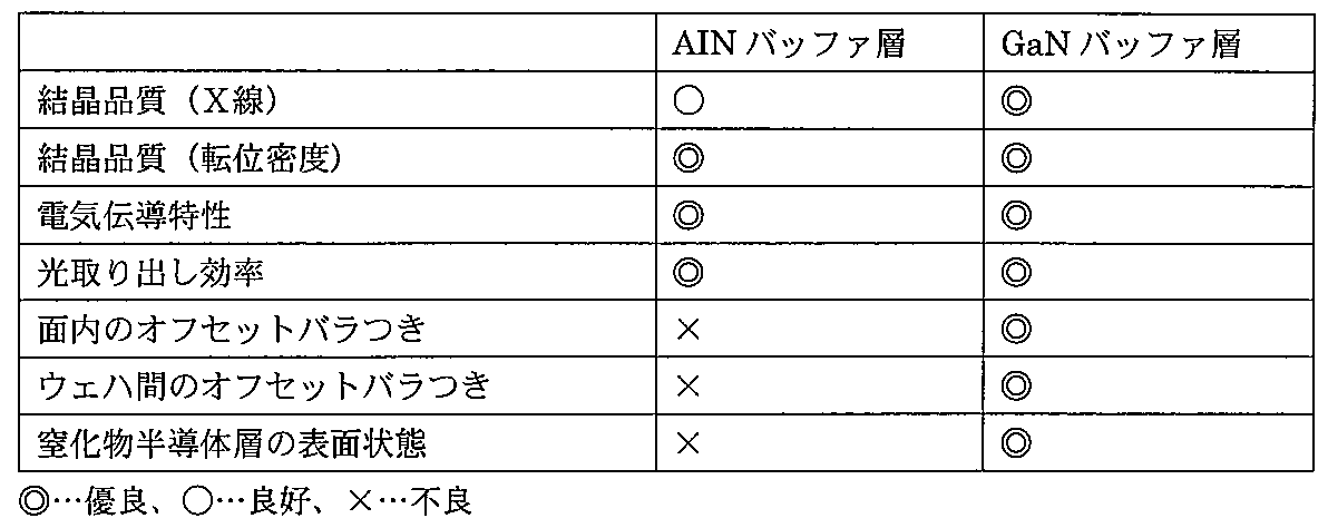
上記表1からも明らかなように、誘電体層3及びGaNバッファ層4を有した構造を用いることで、結晶品質、電気伝導性、光取り出し効率等に優れた窒化物半導体結晶を成長可能であることが分かる。このことは、窒化物半導体層上に形成された半導体素子の信頼性、リーク電流、温度特性、発光効率等で定まる素子特性を総合的に向上させるために非常に重要である。また、面内におけるオフセットのバラつきや表面粗さ等の低減も可能であり、半導体素子を歩留まり高く生産するために非常に効果的であると言える。
[第2の実施の形態]
上記第1の実施の形態に係る半導体積層構造体1は、様々な半導体素子の製造に用いることができる。以下に、その半導体素子の一例として、縦型LEDについて説明する。
上記第1の実施の形態に係る半導体積層構造体1は、様々な半導体素子の製造に用いることができる。以下に、その半導体素子の一例として、縦型LEDについて説明する。
図14は、第2の実施の形態に係る縦型LED10の垂直断面図である。縦型LED10は、Ga2O3基板2と、Ga2O3基板2上の誘電体層3及びGaNバッファ層4と、GaNバッファ層4上のn型クラッド層14と、n型クラッド層14上の発光層15と、発光層15上のp型クラッド層16と、p型クラッド層16上のコンタクト層17と、コンタクト層17上のp型電極18と、Ga2O3基板2のGaNバッファ層4と反対側の面上のn型電極19とを有する。
また、誘電体層3、GaNバッファ層4、n型クラッド層14、発光層15、p型クラッド層16、及びコンタクト層17から構成される積層体の側面は、絶縁膜20に覆われる。
ここで、n型クラッド層14は、第1の実施の形態の半導体積層構造体1を構成する窒化物半導体層5に相当する。Ga2O3基板2、誘電体層3、GaNバッファ層4、及びn型クラッド層14のそれぞれの厚さは、例えば400μm、1μm、48nm、5μmである。
発光層15は、例えば3層の多重量子井戸構造と、その上の厚さ10nmのGaN結晶膜からなる。各多重量子井戸構造は、厚さ6nmのGaN結晶膜と厚さ2nmのInGaN結晶膜からなる。発光層15は、例えば成長温度700~800℃で各結晶膜をn型クラッド層14上にエピタキシャル成長させることにより形成される。
p型クラッド層16は、例えば厚さ100nmの、濃度5.0×10¹⁹/cm3のMgを含むGaN結晶膜である。p型クラッド層16は、例えば成長温度900~1050℃でMgを含むGaN結晶を発光層15上にエピタキシャル成長させることにより形成される。
コンタクト層17は、例えば厚さ10nmの、濃度1.5×10²⁰/cm3のMgを含むGaN結晶膜である。コンタクト層17は、例えば成長温度900~1050℃でMgを含むGaN結晶をp型クラッド層16上にエピタキシャル成長させることにより形成
される。
される。
GaNバッファ層4、n型クラッド層14、発光層15、p型クラッド層16、及びコンタクト層17の形成においては、Ga原料としてTMG(トリメチルガリウム)ガス、In原料としてTMI(トリメチルインジウム)ガス、Si原料としてMtSiH3(モノメチルシラン)ガス、Mg原料としてCp2Mg(ビスシクロペンタジエニルマグネシウム)ガス、N原料としてNH3(アンモニア)ガスを用いることができる。
絶縁膜20は、SiO2等からなる絶縁材料からなり、例えば、スパッタリングにより形成される。
p型電極18及びn型電極19は、それぞれコンタクト層17及びGa2O3基板2にオーミック接合する電極であり、例えば蒸着装置により形成される。
縦型LED10は、ウェハ状態のGa2O3基板2上に、誘電体層3、GaNバッファ層4、n型クラッド層14、発光層15、p型クラッド層16、コンタクト層17、p型電極18、及びn型電極19を形成した後、これらをダイシングによって、例えば300μm角のチップサイズに分離することにより得られる。
縦型LED10は、例えばGa2O3基板2側から光を取り出すLEDチップであり、キャンタイプのステムにAgペーストを用いて実装される。
縦型LED10のn型クラッド層14は、特別なオフセット角度で傾斜した面を主面とするGa2O3基板2上に形成されるため、表面粗さが小さく、かつ優れた結晶品質を有する。また、優れた結晶品質を有するn型クラッド層14上にエピタキシャル結晶成長により形成される発光層15、p型クラッド層16、及びコンタクト層17も優れた結晶品質を有する。このため、LED素子10は、リーク特性及び信頼性に優れる。
(第2の実施の形態の効果)
第2の実施の形態によれば、(-201)面から傾斜した面を主面とするβ-Ga2O3基板上にSiN等による誘電体層構造を備え、GaN結晶からなるバッファ層を用い、AlxGayInzN(0≦x≦1、0≦y≦1、0≦z≦1、x+y+z=1)結晶をエピタキシャル成長させることにより、品質の高い窒化物半導体層を得ることができる。具体的には、X線ロッキングカーブ測定による半値幅が狭く、転位密度が低く、電気伝導特性に優れ、光取り出し効率に優れ、面内におけるオフ角のバラつきが小さく、表面のモフォロジー不良であるヒロックの密度が低減できる。また、ウェハ間のオフ角バラつきも小さく、品質の安定した窒化物半導体層を得ることができる。
第2の実施の形態によれば、(-201)面から傾斜した面を主面とするβ-Ga2O3基板上にSiN等による誘電体層構造を備え、GaN結晶からなるバッファ層を用い、AlxGayInzN(0≦x≦1、0≦y≦1、0≦z≦1、x+y+z=1)結晶をエピタキシャル成長させることにより、品質の高い窒化物半導体層を得ることができる。具体的には、X線ロッキングカーブ測定による半値幅が狭く、転位密度が低く、電気伝導特性に優れ、光取り出し効率に優れ、面内におけるオフ角のバラつきが小さく、表面のモフォロジー不良であるヒロックの密度が低減できる。また、ウェハ間のオフ角バラつきも小さく、品質の安定した窒化物半導体層を得ることができる。
また、このような窒化物半導体層を用いることにより、リーク電流、信頼性、温度特性、発光効率等で定まる総合的な素子特性に優れた半導体素子を歩留まり高く生産することができる。
[第3の実施の形態]
第3の実施の形態として、第1の実施の形態の半導体積層構造体1を含む縦型FET(Field effect transistor)について述べる。
第3の実施の形態として、第1の実施の形態の半導体積層構造体1を含む縦型FET(Field effect transistor)について述べる。
図15は、第3の実施の形態に係る半導体素子である縦型FETの垂直断面図である。縦型FET30は、Ga2O3基板2、誘電体層3、GaNバッファ層4、及び窒化物半導体層(n+-GaN層)5を含む半導体積層構造体1と、窒化物半導体層5の表面(図15における上側の面)上に形成されたGaN系縦型FET31と、GaN系縦型FET31上に形成されたゲート電極32及びソース電極33と、Ga2O3基板2の表面(図15における下側の面)上に形成されたドレイン電極34とを含む。
なお、縦型FET30は、半導体積層構造体1を用いて形成することのできる縦型FETの一例である。
[第4の実施の形態]
第4の実施の形態として、第1の実施の形態の半導体積層構造体1を含むMIS(Metal Insulator Semiconductor)ゲート構造の縦型FETについて述べる。
第4の実施の形態として、第1の実施の形態の半導体積層構造体1を含むMIS(Metal Insulator Semiconductor)ゲート構造の縦型FETについて述べる。
図16は、第4の実施の形態に係る半導体素子である縦型FETの垂直断面図である。縦型FET40は、Ga2O3基板2、誘電体層3、GaNバッファ層4、及び窒化物半導体層(n+-GaN層)5を含む半導体積層構造体1と、窒化物半導体層5中にp型不純物を導入することにより形成されたp+-GaN層41と、窒化物半導体層5の表面(図16における上側の面)上に形成されたAl0.2Ga0.8N層42と、Al0.2Ga0.8N層42中にSi等のn型不純物を導入することにより形成されたSiイオン注入領域43と、Al0.2Ga0.8N層42上にゲート絶縁膜44を介して形成されたゲート電極45と、Siイオン注入領域43及びp+-GaN層41に接続されたソース電極46と、Ga2O3基板2の表面(図16における下側の面)上に形成されたドレイン電極47とを含む。
ここで、窒化物半導体層5の厚さは、例えば5μmであり、Si濃度は1×10¹⁸/cm3である。p+-GaN層41の厚さは、例えば1μmであり、p型不純物の濃度は1×1018/cm3である。Al0.2Ga0.8N層42は不純物を含まず、厚さは、例えば30nmである。ソース電極46は、例えばTi膜とAl膜の積層体からなる。ドレイン電極47は、例えばTi膜とAu膜の積層体からなる。ゲート電極45は、例えばAlからなり、ゲート絶縁膜44は、例えばSiO2からなる。
なお、縦型FET40は、半導体積層構造体1を用いて形成することのできるMISゲート構造の縦型FETの一例である。
[第5の実施の形態]
第5の実施の形態として、第1の実施の形態の半導体積層構造体1を含むショットキーゲート構造の縦型FETについて述べる。
第5の実施の形態として、第1の実施の形態の半導体積層構造体1を含むショットキーゲート構造の縦型FETについて述べる。
図17は、第5の実施の形態に係る半導体素子である縦型FETの垂直断面図である。縦型FET50は、Ga2O3基板2、誘電体層3、GaNバッファ層4、及び窒化物半導体層(n--GaN層)5を含む半導体積層構造体1と、窒化物半導体層5の表面(図17における上側の面)上に積層されたp+-GaN層51、n+-GaN層52、GaN層53、及びAl0.2Ga0.8N層54と、Al0.2Ga0.8N層54上に形成されたゲート電極55と、p+-GaN層51、n+-GaN層52、GaN層53、及びAl0.2Ga0.8N層54に接続されたソース電極56と、Ga2O3基板2の表面(図17における下側の面)上に形成されたドレイン電極57とを含む。
ここで、窒化物半導体層5の厚さは、例えば5μmであり、Si濃度は1×10¹⁶/cm3である。また、p+-GaN層51の厚さは、例えば1μmであり、p型不純物の濃度は1×1018/cm3である。また、n+-GaN層52の厚さは、例えば200nmであり、n型不純物の濃度は1×1018/cm3である。GaN層53は不純物を含まず、厚さは、例えば100nmである。Al0.2Ga0.8N層54は不純物を含まず、厚さは、例えば30nmである。ソース電極56は、例えばTi膜とAl膜の積層体からなる。ドレイン電極57は、例えばTi膜とAu膜の積層体からなる。ゲート電極55は、例えばNi膜とAu膜の積層体からなる。
なお、縦型FET50は、半導体積層構造体1を用いて形成することのできるショットキーゲート構造の縦型FETの一例である。
[第6の実施の形態]
第6の実施の形態として、第1の実施の形態の半導体積層構造体1を含む他のショットキーゲート構造の縦型FETについて述べる。
第6の実施の形態として、第1の実施の形態の半導体積層構造体1を含む他のショットキーゲート構造の縦型FETについて述べる。
図18は、第6の実施の形態に係る半導体素子である縦型FETの垂直断面図である。縦型FET60は、Ga2O3基板2、誘電体層3、GaNバッファ層4、及び窒化物半導体層(n+-GaN層)5を含む半導体積層構造体1と、窒化物半導体層5の表面(図18における上側の面)上に形成されたn--GaN層61と、n--GaN層61の平坦部上に形成されたゲート電極62と、n--GaN層61の凸部上にn+-InAlGaNコンタクト層63を介して形成されたソース電極64と、Ga2O3基板2の表面(図18における下側の面)上に形成されたドレイン電極65とを含む。
ここで、窒化物半導体層5の厚さは、例えば5μmであり、Si濃度は1×10¹⁸/cm3である。また、n--GaN層61の平坦部の厚さは、例えば3μmであり、n型不純物の濃度は1×1016/cm3である。ソース電極64は、例えばWSiからなる。ドレイン電極65は、例えばTi膜とAl膜の積層体からなる。ゲート電極62は、例えばPdSiからなる。
なお、縦型FET60は、半導体積層構造体1を用いて形成することのできるショットキーゲート構造の縦型FETの一例である。
[第7の実施の形態]
第7の実施の形態として、第1の実施の形態の半導体積層構造体1を含むヘテロ接合バイポーラトランジスタ(HBT)について述べる。
第7の実施の形態として、第1の実施の形態の半導体積層構造体1を含むヘテロ接合バイポーラトランジスタ(HBT)について述べる。
図19は、第7の実施の形態に係る半導体素子であるHBTの垂直断面図である。HBT70は、Ga2O3基板2、誘電体層3、GaNバッファ層4、及び窒化物半導体層(n+-GaN層)5を含む半導体積層構造体1と、窒化物半導体層5の表面(図19における上側の面)上に積層されたn--GaN層71及びp+-GaN層72と、p+-GaN層72上に積層されたn+-Al0.1Ga0.9N層73及びn+-GaN層74と、p+-GaN層72上に形成されたベース電極75と、n+-GaN層74上に形成されたエミッタ電極77と、Ga2O3基板2の表面(図19における下側の面)上に形成されたコレクタ電極76とを含む。
ここで、窒化物半導体層5の厚さは、例えば4μmであり、Si濃度は1×10¹⁸/cm3である。また、n--GaN層71の厚さは、例えば2μmであり、n型不純物の濃度は1×1016/cm3である。また、p+-GaN層72の厚さは、例えば100nmであり、p型不純物の濃度は1×1018/cm3である。また、n+-Al0.1Ga0.9N層73の厚さは、例えば500nmであり、n型不純物の濃度は1×1018/cm3である。また、n+-GaN層74の厚さは、例えば1μmであり、n型不純物の濃度は1×1018/cm3である。エミッタ電極77は、例えばTi膜とAl膜の積層体からなる。コレクタ電極76は、例えばTi膜とAu膜の積層体からなる。ベース電極75は、例えばNi膜とAu膜の積層体からなる。
なお、HBT70は、半導体積層構造体1を用いて形成することのできるヘテロ接合バイポーラトランジスタの一例である。
[第8の実施の形態]
第8の実施の形態として、第1の実施の形態の半導体積層構造体1を含むショットキーバリアダイオード(SBD)について述べる。
第8の実施の形態として、第1の実施の形態の半導体積層構造体1を含むショットキーバリアダイオード(SBD)について述べる。
図20は、第8の実施の形態に係る半導体素子であるSBDの断面図である。SBD80は、Ga2O3基板2、誘電体層3、GaNバッファ層4、及び窒化物半導体層(n+-GaN層)5を含む半導体積層構造体1と、窒化物半導体層5の表面(図20における上側の面)上に形成されたn--GaN層81と、n--GaN層81上に形成されたアノード電極82と、Ga2O3基板2の表面(図20における下側の面)上に形成されたカソード電極83とを含む。
ここで、窒化物半導体層5の厚さは、例えば5μmであり、Si濃度は1×10¹⁸/cm3である。また、n--GaN層81の厚さは、例えば7μmであり、n型不純物の濃度は1×1016/cm3である。アノード電極82は、例えばAuからなる。カソード電極83は、例えばTi膜とAu膜の積層体からなる。
なお、SBD80は、半導体積層構造体1を用いて形成することのできるショットキーバリアダイオードの一例である。
(第3~第8の実施の形態の効果)
(-201)面から傾斜した面を主面とするβ-Ga2O3基板上にSiN等による誘電体層構造を備え、GaN結晶からなるバッファ層を用い、AlxGayInzN(0≦x≦1、0≦y≦1、0≦z≦1、x+y+z=1)結晶をエピタキシャル成長させることにより、品質の高い窒化物半導体層を得ることができる。具体的には、X線ロッキングカーブ測定による半値幅が狭く、転位密度が低く、電気伝導特性に優れ、面内におけるオフ角のバラつきが小さく、表面のモフォロジー不良であるヒロックの密度が低減できる。また、ウェハ間のオフ角バラつきも小さく、品質の安定した窒化物半導体層を得ることができる。また、このような半導体積層構造体を用いることにより、信頼性、リーク電流、温度特性等の素子特性を総合的に向上させることができる。
(-201)面から傾斜した面を主面とするβ-Ga2O3基板上にSiN等による誘電体層構造を備え、GaN結晶からなるバッファ層を用い、AlxGayInzN(0≦x≦1、0≦y≦1、0≦z≦1、x+y+z=1)結晶をエピタキシャル成長させることにより、品質の高い窒化物半導体層を得ることができる。具体的には、X線ロッキングカーブ測定による半値幅が狭く、転位密度が低く、電気伝導特性に優れ、面内におけるオフ角のバラつきが小さく、表面のモフォロジー不良であるヒロックの密度が低減できる。また、ウェハ間のオフ角バラつきも小さく、品質の安定した窒化物半導体層を得ることができる。また、このような半導体積層構造体を用いることにより、信頼性、リーク電流、温度特性等の素子特性を総合的に向上させることができる。
以上の説明からも明らかなように、本発明に係る代表的な各実施の形態及び図示例を例示したが、上記各実施の形態及び図示例は請求の範囲に係る発明を限定するものではない。従って、上記各実施の形態及び図示例の中で説明した特徴の組合せの全てが発明の課題を解決するための手段に必須であるとは限らない点に留意すべきである。
信頼性、リーク電流、温度特性、発光効率等で定まる素子特性を総合的に向上させることが可能な、品質が高く、かつ面内において均一性の高い窒化物半導体層を有する半導体積層構造体、及びその半導体積層構造体を含む半導体素子を提供する。
1…半導体積層構造体、2…Ga2O3基板、3…誘電体層、4…GaNバッファ層、5…窒化物半導体層、6…レジストパターン、10…縦型LED、14…n型クラッド層、15…発光層、16…p型クラッド層、17…コンタクト層、18…p型電極、19…n型電極、20…絶縁膜、30,40,50,60…縦型FET、31…GaN系縦型FET、32…ゲート電極、33…ソース電極、34…ドレイン電極、41,51…p+-GaN層、42…Al0.2Ga0.8N層、43…Siイオン注入領域、44…ゲート絶縁膜、45,55,62…ゲート電極、46,56,64…ソース電極、47,57,65…ドレイン電極、52,74…n+-GaN層、53…GaN層、54…Al0.2Ga0.8N層、61,71,81…n--GaN層、63…n+-InAlGaNコンタクト層、70…HBT、72…p+-GaN層、73…n+-Al0.1Ga0.9N層、75…ベース電極、77…エミッタ電極、76…コレクタ電極、80…ショットキーバリアダイオード、82…アノード電極、83…カソード電極
Claims (6)
- Ga2O3基板と、
前記Ga2O3基板の上面に部分的に接触するように形成され、前記Ga2O3基板との屈折率の差が0.15以下である誘電体層と、
前記Ga2O3基板の前記誘電体層に覆われていない残りの上面に接触するように形成されたGaN結晶からなるバッファ層と、
前記Ga2O3基板上に前記バッファ層を介して形成されたAlxGayInzN(0≦x≦1、0≦y≦1、0≦z≦1、x+y+z=1)結晶からなる窒化物半導体層と、を有する半導体積層構造体。 - 前記窒化物半導体層は、X線ロッキングカーブ測定において(002)面回折の半値幅が270秒以下である請求項1に記載の半導体積層構造体。
- 前記窒化物半導体層は、X線ロッキングカーブ測定において(101)面回折の半値幅が270秒以下である請求項1又は2に記載の半導体積層構造体。
- 前記誘電体層は、SiNを主成分とするSiN層からなる請求項1~3のいずれか1項に記載の半導体積層構造体。
- 前記窒化物半導体層は、GaN結晶からなる請求項1~4のいずれか1項に記載の半導体積層構造体。
- 上記請求項1~5のいずれか1項に記載の半導体積層構造体を含む半導体素子。
Applications Claiming Priority (2)
| Application Number | Priority Date | Filing Date | Title |
|---|---|---|---|
| JP2014135957A JP2016015374A (ja) | 2014-07-01 | 2014-07-01 | 半導体積層構造体及び半導体素子 |
| JP2014-135957 | 2014-07-01 |
Publications (1)
| Publication Number | Publication Date |
|---|---|
| WO2016002801A1 true WO2016002801A1 (ja) | 2016-01-07 |
Family
ID=55019332
Family Applications (1)
| Application Number | Title | Priority Date | Filing Date |
|---|---|---|---|
| PCT/JP2015/068881 Ceased WO2016002801A1 (ja) | 2014-07-01 | 2015-06-30 | 半導体積層構造体及び半導体素子 |
Country Status (2)
| Country | Link |
|---|---|
| JP (1) | JP2016015374A (ja) |
| WO (1) | WO2016002801A1 (ja) |
Cited By (1)
| Publication number | Priority date | Publication date | Assignee | Title |
|---|---|---|---|---|
| US20220028700A1 (en) * | 2019-04-08 | 2022-01-27 | AGC Inc. | Gallium oxide substrate and method of manufacturing gallium oxide substrate |
Families Citing this family (2)
| Publication number | Priority date | Publication date | Assignee | Title |
|---|---|---|---|---|
| JP6811646B2 (ja) * | 2017-02-28 | 2021-01-13 | 株式会社タムラ製作所 | 窒化物半導体テンプレート及びその製造方法 |
| JP7486121B2 (ja) * | 2020-06-05 | 2024-05-17 | 株式会社Flosfia | 半導体装置 |
Citations (7)
| Publication number | Priority date | Publication date | Assignee | Title |
|---|---|---|---|---|
| JP2004247493A (ja) * | 2003-02-13 | 2004-09-02 | Ngk Insulators Ltd | エピタキシャル基板、半導体積層構造及びiii族窒化物層群の転位低減方法 |
| JP2004297010A (ja) * | 2003-03-28 | 2004-10-21 | Toyoda Gosei Co Ltd | 半導体結晶の製造方法及び半導体発光素子 |
| JP2010087292A (ja) * | 2008-09-30 | 2010-04-15 | Toyoda Gosei Co Ltd | 発光素子 |
| JP2010114423A (ja) * | 2008-10-09 | 2010-05-20 | Canon Inc | ウルツ鉱型結晶成長用基板およびその製造方法ならびに半導体装置 |
| JP2011060917A (ja) * | 2009-09-08 | 2011-03-24 | Rohm Co Ltd | 半導体発光素子 |
| WO2012093601A1 (ja) * | 2011-01-07 | 2012-07-12 | 三菱化学株式会社 | エピタキシャル成長用基板およびGaN系LEDデバイス |
| JP2014022446A (ja) * | 2012-07-13 | 2014-02-03 | Tamura Seisakusho Co Ltd | 半導体積層構造体及び発光素子 |
-
2014
- 2014-07-01 JP JP2014135957A patent/JP2016015374A/ja active Pending
-
2015
- 2015-06-30 WO PCT/JP2015/068881 patent/WO2016002801A1/ja not_active Ceased
Patent Citations (7)
| Publication number | Priority date | Publication date | Assignee | Title |
|---|---|---|---|---|
| JP2004247493A (ja) * | 2003-02-13 | 2004-09-02 | Ngk Insulators Ltd | エピタキシャル基板、半導体積層構造及びiii族窒化物層群の転位低減方法 |
| JP2004297010A (ja) * | 2003-03-28 | 2004-10-21 | Toyoda Gosei Co Ltd | 半導体結晶の製造方法及び半導体発光素子 |
| JP2010087292A (ja) * | 2008-09-30 | 2010-04-15 | Toyoda Gosei Co Ltd | 発光素子 |
| JP2010114423A (ja) * | 2008-10-09 | 2010-05-20 | Canon Inc | ウルツ鉱型結晶成長用基板およびその製造方法ならびに半導体装置 |
| JP2011060917A (ja) * | 2009-09-08 | 2011-03-24 | Rohm Co Ltd | 半導体発光素子 |
| WO2012093601A1 (ja) * | 2011-01-07 | 2012-07-12 | 三菱化学株式会社 | エピタキシャル成長用基板およびGaN系LEDデバイス |
| JP2014022446A (ja) * | 2012-07-13 | 2014-02-03 | Tamura Seisakusho Co Ltd | 半導体積層構造体及び発光素子 |
Cited By (1)
| Publication number | Priority date | Publication date | Assignee | Title |
|---|---|---|---|---|
| US20220028700A1 (en) * | 2019-04-08 | 2022-01-27 | AGC Inc. | Gallium oxide substrate and method of manufacturing gallium oxide substrate |
Also Published As
| Publication number | Publication date |
|---|---|
| JP2016015374A (ja) | 2016-01-28 |
Similar Documents
| Publication | Publication Date | Title |
|---|---|---|
| TWI476947B (zh) | An epitaxial wafer, a gallium nitride-based semiconductor device, a gallium nitride-based semiconductor device, and a gallium oxide wafer | |
| US6635901B2 (en) | Semiconductor device including an InGaAIN layer | |
| JP5596222B2 (ja) | 半導体積層体及びその製造方法、並びに半導体素子 | |
| JP5099008B2 (ja) | SiC基板を用いた化合物半導体装置とその製造方法 | |
| CN102484049A (zh) | 半导体元件用外延基板、半导体元件用外延基板的制造方法以及半导体元件 | |
| US20150349064A1 (en) | Nucleation and buffer layers for group iii-nitride based semiconductor devices | |
| US8680569B2 (en) | Method for manufacturing gallium oxide based substrate, light emitting device, and method for manufacturing the light emitting device | |
| US20100301393A1 (en) | Field effect transistor and manufacturing method therefor | |
| JP4210823B2 (ja) | シヨットキバリアダイオード及びその製造方法 | |
| CN103839979A (zh) | 氮化物半导体器件、氮化物半导体晶片和形成氮化物半导体层的方法 | |
| JP5401145B2 (ja) | Iii族窒化物積層体の製造方法 | |
| CN111463326A (zh) | 半导体器件及其制备方法 | |
| JP5460751B2 (ja) | 半導体装置 | |
| JP6089122B2 (ja) | 窒化物半導体積層体およびその製造方法並びに窒化物半導体装置 | |
| JP2016015374A (ja) | 半導体積層構造体及び半導体素子 | |
| CN101276864A (zh) | 发光元件 | |
| CN109473511B (zh) | 一种氮化镓基发光二极管外延片及其生长方法 | |
| TW202107734A (zh) | 發光二極體及其製造方法 | |
| TWI545798B (zh) | Nitride semiconductor light emitting device and manufacturing method thereof | |
| JP5059205B2 (ja) | ウェーハ及び結晶成長方法 | |
| US20140027770A1 (en) | Semiconductor laminate and process for production thereof, and semiconductor element | |
| KR101901932B1 (ko) | 이종 기판, 질화물 반도체 발광 소자 및 그 제조 방법 | |
| CN109346573A (zh) | 一种氮化镓基发光二极管外延片及其制备方法 | |
| CN109473525A (zh) | 一种氮化镓基发光二极管外延片及其制作方法 | |
| KR20100105073A (ko) | 질화물 반도체 기판, 이의 제조방법 및 질화물 반도체 기판을 구비하는 발광 다이오드 |
Legal Events
| Date | Code | Title | Description |
|---|---|---|---|
| 121 | Ep: the epo has been informed by wipo that ep was designated in this application |
Ref document number: 15814819 Country of ref document: EP Kind code of ref document: A1 |
|
| NENP | Non-entry into the national phase |
Ref country code: DE |
|
| 122 | Ep: pct application non-entry in european phase |
Ref document number: 15814819 Country of ref document: EP Kind code of ref document: A1 |