WO2015194128A1 - アクティブマトリクス型表示パネルの製造方法とアクティブマトリクス型表示パネル - Google Patents
アクティブマトリクス型表示パネルの製造方法とアクティブマトリクス型表示パネル Download PDFInfo
- Publication number
- WO2015194128A1 WO2015194128A1 PCT/JP2015/002895 JP2015002895W WO2015194128A1 WO 2015194128 A1 WO2015194128 A1 WO 2015194128A1 JP 2015002895 W JP2015002895 W JP 2015002895W WO 2015194128 A1 WO2015194128 A1 WO 2015194128A1
- Authority
- WO
- WIPO (PCT)
- Prior art keywords
- layer
- contact hole
- passivation layer
- electrode
- display panel
- Prior art date
- Legal status (The legal status is an assumption and is not a legal conclusion. Google has not performed a legal analysis and makes no representation as to the accuracy of the status listed.)
- Ceased
Links
Images







Classifications
-
- H—ELECTRICITY
- H10—SEMICONDUCTOR DEVICES; ELECTRIC SOLID-STATE DEVICES NOT OTHERWISE PROVIDED FOR
- H10D—INORGANIC ELECTRIC SEMICONDUCTOR DEVICES
- H10D86/00—Integrated devices formed in or on insulating or conducting substrates, e.g. formed in silicon-on-insulator [SOI] substrates or on stainless steel or glass substrates
- H10D86/01—Manufacture or treatment
- H10D86/021—Manufacture or treatment of multiple TFTs
-
- H—ELECTRICITY
- H05—ELECTRIC TECHNIQUES NOT OTHERWISE PROVIDED FOR
- H05B—ELECTRIC HEATING; ELECTRIC LIGHT SOURCES NOT OTHERWISE PROVIDED FOR; CIRCUIT ARRANGEMENTS FOR ELECTRIC LIGHT SOURCES, IN GENERAL
- H05B45/00—Circuit arrangements for operating light-emitting diodes [LED]
- H05B45/20—Controlling the colour of the light
-
- H—ELECTRICITY
- H05—ELECTRIC TECHNIQUES NOT OTHERWISE PROVIDED FOR
- H05B—ELECTRIC HEATING; ELECTRIC LIGHT SOURCES NOT OTHERWISE PROVIDED FOR; CIRCUIT ARRANGEMENTS FOR ELECTRIC LIGHT SOURCES, IN GENERAL
- H05B45/00—Circuit arrangements for operating light-emitting diodes [LED]
- H05B45/60—Circuit arrangements for operating LEDs comprising organic material, e.g. for operating organic light-emitting diodes [OLED] or polymer light-emitting diodes [PLED]
-
- H—ELECTRICITY
- H10—SEMICONDUCTOR DEVICES; ELECTRIC SOLID-STATE DEVICES NOT OTHERWISE PROVIDED FOR
- H10D—INORGANIC ELECTRIC SEMICONDUCTOR DEVICES
- H10D30/00—Field-effect transistors [FET]
- H10D30/60—Insulated-gate field-effect transistors [IGFET]
- H10D30/67—Thin-film transistors [TFT]
- H10D30/674—Thin-film transistors [TFT] characterised by the active materials
- H10D30/6755—Oxide semiconductors, e.g. zinc oxide, copper aluminium oxide or cadmium stannate
- H10D30/6756—Amorphous oxide semiconductors
-
- H—ELECTRICITY
- H10—SEMICONDUCTOR DEVICES; ELECTRIC SOLID-STATE DEVICES NOT OTHERWISE PROVIDED FOR
- H10D—INORGANIC ELECTRIC SEMICONDUCTOR DEVICES
- H10D86/00—Integrated devices formed in or on insulating or conducting substrates, e.g. formed in silicon-on-insulator [SOI] substrates or on stainless steel or glass substrates
- H10D86/40—Integrated devices formed in or on insulating or conducting substrates, e.g. formed in silicon-on-insulator [SOI] substrates or on stainless steel or glass substrates characterised by multiple TFTs
- H10D86/421—Integrated devices formed in or on insulating or conducting substrates, e.g. formed in silicon-on-insulator [SOI] substrates or on stainless steel or glass substrates characterised by multiple TFTs having a particular composition, shape or crystalline structure of the active layer
- H10D86/423—Integrated devices formed in or on insulating or conducting substrates, e.g. formed in silicon-on-insulator [SOI] substrates or on stainless steel or glass substrates characterised by multiple TFTs having a particular composition, shape or crystalline structure of the active layer comprising semiconductor materials not belonging to the Group IV, e.g. InGaZnO
-
- H—ELECTRICITY
- H10—SEMICONDUCTOR DEVICES; ELECTRIC SOLID-STATE DEVICES NOT OTHERWISE PROVIDED FOR
- H10D—INORGANIC ELECTRIC SEMICONDUCTOR DEVICES
- H10D86/00—Integrated devices formed in or on insulating or conducting substrates, e.g. formed in silicon-on-insulator [SOI] substrates or on stainless steel or glass substrates
- H10D86/40—Integrated devices formed in or on insulating or conducting substrates, e.g. formed in silicon-on-insulator [SOI] substrates or on stainless steel or glass substrates characterised by multiple TFTs
- H10D86/451—Integrated devices formed in or on insulating or conducting substrates, e.g. formed in silicon-on-insulator [SOI] substrates or on stainless steel or glass substrates characterised by multiple TFTs characterised by the compositions or shapes of the interlayer dielectrics
-
- H—ELECTRICITY
- H10—SEMICONDUCTOR DEVICES; ELECTRIC SOLID-STATE DEVICES NOT OTHERWISE PROVIDED FOR
- H10D—INORGANIC ELECTRIC SEMICONDUCTOR DEVICES
- H10D86/00—Integrated devices formed in or on insulating or conducting substrates, e.g. formed in silicon-on-insulator [SOI] substrates or on stainless steel or glass substrates
- H10D86/40—Integrated devices formed in or on insulating or conducting substrates, e.g. formed in silicon-on-insulator [SOI] substrates or on stainless steel or glass substrates characterised by multiple TFTs
- H10D86/60—Integrated devices formed in or on insulating or conducting substrates, e.g. formed in silicon-on-insulator [SOI] substrates or on stainless steel or glass substrates characterised by multiple TFTs wherein the TFTs are in active matrices
-
- H—ELECTRICITY
- H10—SEMICONDUCTOR DEVICES; ELECTRIC SOLID-STATE DEVICES NOT OTHERWISE PROVIDED FOR
- H10K—ORGANIC ELECTRIC SOLID-STATE DEVICES
- H10K59/00—Integrated devices, or assemblies of multiple devices, comprising at least one organic light-emitting element covered by group H10K50/00
- H10K59/10—OLED displays
- H10K59/12—Active-matrix OLED [AMOLED] displays
-
- H—ELECTRICITY
- H10—SEMICONDUCTOR DEVICES; ELECTRIC SOLID-STATE DEVICES NOT OTHERWISE PROVIDED FOR
- H10K—ORGANIC ELECTRIC SOLID-STATE DEVICES
- H10K59/00—Integrated devices, or assemblies of multiple devices, comprising at least one organic light-emitting element covered by group H10K50/00
- H10K59/10—OLED displays
- H10K59/12—Active-matrix OLED [AMOLED] displays
- H10K59/122—Pixel-defining structures or layers, e.g. banks
-
- H—ELECTRICITY
- H10—SEMICONDUCTOR DEVICES; ELECTRIC SOLID-STATE DEVICES NOT OTHERWISE PROVIDED FOR
- H10K—ORGANIC ELECTRIC SOLID-STATE DEVICES
- H10K59/00—Integrated devices, or assemblies of multiple devices, comprising at least one organic light-emitting element covered by group H10K50/00
- H10K59/10—OLED displays
- H10K59/12—Active-matrix OLED [AMOLED] displays
- H10K59/124—Insulating layers formed between TFT elements and OLED elements
-
- H—ELECTRICITY
- H10—SEMICONDUCTOR DEVICES; ELECTRIC SOLID-STATE DEVICES NOT OTHERWISE PROVIDED FOR
- H10K—ORGANIC ELECTRIC SOLID-STATE DEVICES
- H10K59/00—Integrated devices, or assemblies of multiple devices, comprising at least one organic light-emitting element covered by group H10K50/00
- H10K59/10—OLED displays
- H10K59/12—Active-matrix OLED [AMOLED] displays
- H10K59/127—Active-matrix OLED [AMOLED] displays comprising two substrates, e.g. display comprising OLED array and TFT driving circuitry on different substrates
-
- H—ELECTRICITY
- H10—SEMICONDUCTOR DEVICES; ELECTRIC SOLID-STATE DEVICES NOT OTHERWISE PROVIDED FOR
- H10P—GENERIC PROCESSES OR APPARATUS FOR THE MANUFACTURE OR TREATMENT OF DEVICES COVERED BY CLASS H10
- H10P50/00—Etching of wafers, substrates or parts of devices
- H10P50/20—Dry etching; Plasma etching; Reactive-ion etching
- H10P50/28—Dry etching; Plasma etching; Reactive-ion etching of insulating materials
- H10P50/282—Dry etching; Plasma etching; Reactive-ion etching of insulating materials of inorganic materials
- H10P50/283—Dry etching; Plasma etching; Reactive-ion etching of insulating materials of inorganic materials by chemical means
-
- H—ELECTRICITY
- H10—SEMICONDUCTOR DEVICES; ELECTRIC SOLID-STATE DEVICES NOT OTHERWISE PROVIDED FOR
- H10P—GENERIC PROCESSES OR APPARATUS FOR THE MANUFACTURE OR TREATMENT OF DEVICES COVERED BY CLASS H10
- H10P50/00—Etching of wafers, substrates or parts of devices
- H10P50/20—Dry etching; Plasma etching; Reactive-ion etching
- H10P50/28—Dry etching; Plasma etching; Reactive-ion etching of insulating materials
- H10P50/286—Dry etching; Plasma etching; Reactive-ion etching of insulating materials of organic materials
- H10P50/287—Dry etching; Plasma etching; Reactive-ion etching of insulating materials of organic materials by chemical means
-
- H—ELECTRICITY
- H10—SEMICONDUCTOR DEVICES; ELECTRIC SOLID-STATE DEVICES NOT OTHERWISE PROVIDED FOR
- H10P—GENERIC PROCESSES OR APPARATUS FOR THE MANUFACTURE OR TREATMENT OF DEVICES COVERED BY CLASS H10
- H10P70/00—Cleaning of wafers, substrates or parts of devices
- H10P70/10—Cleaning before device manufacture, i.e. Begin-Of-Line process
- H10P70/15—Cleaning before device manufacture, i.e. Begin-Of-Line process by wet cleaning only
-
- H—ELECTRICITY
- H10—SEMICONDUCTOR DEVICES; ELECTRIC SOLID-STATE DEVICES NOT OTHERWISE PROVIDED FOR
- H10P—GENERIC PROCESSES OR APPARATUS FOR THE MANUFACTURE OR TREATMENT OF DEVICES COVERED BY CLASS H10
- H10P70/00—Cleaning of wafers, substrates or parts of devices
- H10P70/20—Cleaning during device manufacture
- H10P70/23—Cleaning during device manufacture during, before or after processing of insulating materials
- H10P70/234—Cleaning during device manufacture during, before or after processing of insulating materials the processing being the formation of vias or contact holes
-
- H—ELECTRICITY
- H10—SEMICONDUCTOR DEVICES; ELECTRIC SOLID-STATE DEVICES NOT OTHERWISE PROVIDED FOR
- H10W—GENERIC PACKAGES, INTERCONNECTIONS, CONNECTORS OR OTHER CONSTRUCTIONAL DETAILS OF DEVICES COVERED BY CLASS H10
- H10W20/00—Interconnections in chips, wafers or substrates
- H10W20/01—Manufacture or treatment
-
- G—PHYSICS
- G02—OPTICS
- G02F—OPTICAL DEVICES OR ARRANGEMENTS FOR THE CONTROL OF LIGHT BY MODIFICATION OF THE OPTICAL PROPERTIES OF THE MEDIA OF THE ELEMENTS INVOLVED THEREIN; NON-LINEAR OPTICS; FREQUENCY-CHANGING OF LIGHT; OPTICAL LOGIC ELEMENTS; OPTICAL ANALOGUE/DIGITAL CONVERTERS
- G02F1/00—Devices or arrangements for the control of the intensity, colour, phase, polarisation or direction of light arriving from an independent light source, e.g. switching, gating or modulating; Non-linear optics
- G02F1/01—Devices or arrangements for the control of the intensity, colour, phase, polarisation or direction of light arriving from an independent light source, e.g. switching, gating or modulating; Non-linear optics for the control of the intensity, phase, polarisation or colour
- G02F1/13—Devices or arrangements for the control of the intensity, colour, phase, polarisation or direction of light arriving from an independent light source, e.g. switching, gating or modulating; Non-linear optics for the control of the intensity, phase, polarisation or colour based on liquid crystals, e.g. single liquid crystal display cells
- G02F1/133—Constructional arrangements; Operation of liquid crystal cells; Circuit arrangements
- G02F1/136—Liquid crystal cells structurally associated with a semi-conducting layer or substrate, e.g. cells forming part of an integrated circuit
- G02F1/1362—Active matrix addressed cells
- G02F1/136227—Through-hole connection of the pixel electrode to the active element through an insulation layer
-
- G—PHYSICS
- G02—OPTICS
- G02F—OPTICAL DEVICES OR ARRANGEMENTS FOR THE CONTROL OF LIGHT BY MODIFICATION OF THE OPTICAL PROPERTIES OF THE MEDIA OF THE ELEMENTS INVOLVED THEREIN; NON-LINEAR OPTICS; FREQUENCY-CHANGING OF LIGHT; OPTICAL LOGIC ELEMENTS; OPTICAL ANALOGUE/DIGITAL CONVERTERS
- G02F1/00—Devices or arrangements for the control of the intensity, colour, phase, polarisation or direction of light arriving from an independent light source, e.g. switching, gating or modulating; Non-linear optics
- G02F1/01—Devices or arrangements for the control of the intensity, colour, phase, polarisation or direction of light arriving from an independent light source, e.g. switching, gating or modulating; Non-linear optics for the control of the intensity, phase, polarisation or colour
- G02F1/13—Devices or arrangements for the control of the intensity, colour, phase, polarisation or direction of light arriving from an independent light source, e.g. switching, gating or modulating; Non-linear optics for the control of the intensity, phase, polarisation or colour based on liquid crystals, e.g. single liquid crystal display cells
- G02F1/133—Constructional arrangements; Operation of liquid crystal cells; Circuit arrangements
- G02F1/136—Liquid crystal cells structurally associated with a semi-conducting layer or substrate, e.g. cells forming part of an integrated circuit
- G02F1/1362—Active matrix addressed cells
- G02F1/1368—Active matrix addressed cells in which the switching element is a three-electrode device
-
- H—ELECTRICITY
- H10—SEMICONDUCTOR DEVICES; ELECTRIC SOLID-STATE DEVICES NOT OTHERWISE PROVIDED FOR
- H10K—ORGANIC ELECTRIC SOLID-STATE DEVICES
- H10K50/00—Organic light-emitting devices
- H10K50/10—OLEDs or polymer light-emitting diodes [PLED]
-
- H—ELECTRICITY
- H10—SEMICONDUCTOR DEVICES; ELECTRIC SOLID-STATE DEVICES NOT OTHERWISE PROVIDED FOR
- H10K—ORGANIC ELECTRIC SOLID-STATE DEVICES
- H10K50/00—Organic light-emitting devices
- H10K50/10—OLEDs or polymer light-emitting diodes [PLED]
- H10K50/14—Carrier transporting layers
-
- H—ELECTRICITY
- H10—SEMICONDUCTOR DEVICES; ELECTRIC SOLID-STATE DEVICES NOT OTHERWISE PROVIDED FOR
- H10K—ORGANIC ELECTRIC SOLID-STATE DEVICES
- H10K59/00—Integrated devices, or assemblies of multiple devices, comprising at least one organic light-emitting element covered by group H10K50/00
- H10K59/10—OLED displays
- H10K59/12—Active-matrix OLED [AMOLED] displays
- H10K59/1201—Manufacture or treatment
-
- H—ELECTRICITY
- H10—SEMICONDUCTOR DEVICES; ELECTRIC SOLID-STATE DEVICES NOT OTHERWISE PROVIDED FOR
- H10K—ORGANIC ELECTRIC SOLID-STATE DEVICES
- H10K59/00—Integrated devices, or assemblies of multiple devices, comprising at least one organic light-emitting element covered by group H10K50/00
- H10K59/10—OLED displays
- H10K59/12—Active-matrix OLED [AMOLED] displays
- H10K59/123—Connection of the pixel electrodes to the thin film transistors [TFT]
Definitions
- the present invention relates to a method for manufacturing an active matrix display panel and an active matrix display panel.
- the present invention relates to two insulating layers interposed between an electrode of a TFT layer and an electrode of a display element portion, and an interelectrode contact is provided.
- the present invention relates to a technology related to contact hole formation.
- a TFT layer is formed on the upper surface of the substrate 900.
- the TFT layer has a gate electrode 901, a gate insulating layer 902, a channel layer 903, a channel protective layer 904, a source electrode 905 and a drain electrode 906, an interlayer insulating layer 907, an upper electrode 908, and a passivation layer 909 in this order from the substrate 900 side. It has a formed configuration.
- an organic light emitting part (display element part) is formed on the passivation layer 909 in the TFT layer with the planarization layer 910 interposed therebetween.
- the organic light emitting unit has a configuration in which an anode 911, a bank 912, an organic light emitting functional layer 913, a cathode 914, and a sealing layer 915 are formed in this order from the passivation layer 909 side.
- a color filter substrate (CF substrate) is disposed on the organic light emitting unit with the resin layer 916 interposed therebetween.
- the CF substrate has a structure in which a color filter layer 917 and a black matrix layer 918 are formed on the lower surface of the substrate 919.
- the upper electrode 908 in the TFT layer is connected to the source electrode 905, and is also connected to the anode 911 through a contact hole formed in the passivation layer 909 and the planarization layer 910.
- the contact hole is formed by opening a contact hole in the planarization layer 910 by lithography and then opening a contact hole communicating with the passivation layer 909 by dry etching using the planarization layer 910 in which the contact hole is opened as a mask. It is done with.
- the upper electrode 908 and the anode 911 in the TFT layer are formed at the bottom of the contact hole.
- a metal oxide film 922 may be formed. If the metal oxide film 922 is interposed between the upper electrode 908 and the anode 911 in this manner, a connection failure between the upper electrode 908 and the anode 911 occurs, and the display quality of the display panel is degraded.
- the present invention is intended to solve the above-described problems, and a contact hole is formed in two insulating layers interposed between an electrode of a TFT layer and an electrode of a display element portion.
- An active matrix display panel manufacturing method includes (i) a step of forming a TFT layer on a substrate, (ii) a step of forming a planarization layer on the TFT layer, and (iii) Forming a display element portion on the planarization layer.
- the passivation layer that covers either the source electrode or the drain electrode or the connection electrode connected to one of the electrodes is in contact with the planarization layer
- the sub-process of forming is included.
- the step of forming the display element portion includes a sub-step of forming the lower electrode in a state in contact with the planarization layer.
- connection between any of the above electrodes and the lower electrode is made through the following steps.
- the passivation layer exposed at the bottom of the contact hole established in the planarization layer is communicated with the contact hole of the planarization layer by dry etching using a gas containing fluorine, and any of the above is applied to the bottom. Open a contact hole to expose the electrode.
- the lower electrode is formed along the inner wall surface of the planarization layer and the passivation layer facing the contact hole.
- the contact hole is opened with a gas containing fluorine. Therefore, after the contact hole is opened to the passivation layer of (iv-2), at least the inner wall surface facing the contact hole in the planarization layer is formed. A liquid repellent film containing fluorine is formed in the composition. For this reason, even if moisture enters the contact holes of the planarization layer and the passivation layer, the liquid repellent film wets the moisture on the inner wall surface facing the contact hole and the surface of any of the electrodes exposed to the bottom. Can be suppressed.
- an active matrix display panel that can be manufactured can be manufactured.
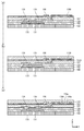
- Parts (a) to (e) are schematic cross-sectional views sequentially showing the manufacturing process of the display panel 10 according to the embodiment of the present invention.
- Parts (a) to (d) are schematic cross-sectional views sequentially showing the manufacturing process of the display panel 10 according to the embodiment of the present invention.
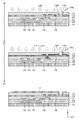
- Parts (a) to (c) are schematic cross-sectional views sequentially showing the manufacturing process of the display panel 10 according to the embodiment of the present invention.
- Parts (a) to (c) are schematic cross-sectional views sequentially showing the manufacturing process of the display panel 10 according to the embodiment of the present invention.
- Parts (a) to (c) are schematic cross-sectional views sequentially showing the manufacturing process of the display panel 10 according to the embodiment of the present invention.
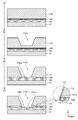
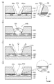
- FIG. Parts (a) to (d) are schematic cross-sectional views sequentially illustrating processes related to formation of contact holes in the passivation layer 1090 and the planarization layer 1100 according to the embodiment.
- Parts (a) to (c) are schematic cross-sectional views sequentially illustrating processes related to formation of contact holes in the passivation layer 1090 and the planarization layer 1100 according to the embodiment.
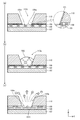
- Parts (a) to (d) are schematic cross-sectional views sequentially illustrating processes related to contact hole formation according to a comparative example.
- A is the image which shows the contact hole formed using the manufacturing method which concerns on an Example, and its periphery by planar view
- (b) is an image which shows the cross section
- (c) is a comparative example It is an image which shows the contact hole formed using the manufacturing method concerning and its periphery in planar view
- (d) is an image which shows the cross section. It is a graph which shows the composition of the upper electrode 108 exposed to the bottom of a contact hole.
- (A) is a schematic cross-sectional view showing the periphery of the contact hole when formed under the conditions according to the embodiment of the present invention
- (b) is the periphery of the contact hole when formed under the conditions according to the comparative example
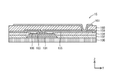
- It is a schematic cross section which shows. It is a schematic cross section which shows a partial structure of the display panel 15 which concerns on a modification. It is a schematic cross section which shows the structure of the display panel which concerns on a prior art.
- the inventors have a problem as shown in a portion surrounded by a two-dot chain line in FIG. 14, that is, a metal oxide film 922 is interposed between the upper electrode 908 and the anode electrode 911 in the TFT layer.
- the mechanism of the contact failure between 908 and the anode 911 was elucidated as follows.
- a contact hole for making contact between the upper electrode 908 and the anode 911 is opened.
- the contact hole is formed by opening a contact hole in the planarization layer 910 by lithography (exposure / development) and then opening a contact hole in the passivation layer 909 exposed at the bottom of the contact hole of the planarization layer 910 by dry etching. That is done. Then, after the dry etching, the inside of the hole and the surface of the planarizing layer 910 are cleaned using, for example, pure water.
- the inner wall surface of the planarization layer 910 that faces the contact hole is opened first, and the contact hole is exposed to the etching gas containing fluorine during the opening of the contact hole to the passivation layer 909.
- a fluoride film has been formed.
- the contact hole is also blown by dry air. It is thought that water may remain at the bottom. Then, the water remaining at the bottom of the contact hole is considered to oxidize the surface of the upper electrode 908 and form the metal oxide film 922.
- An active matrix display panel manufacturing method includes: (i) a step of forming a TFT layer on a substrate; (ii) a step of forming a planarization layer on the TFT layer; and (iii) Forming a display element portion on the planarization layer; Is provided.
- the source electrode or the drain electrode, or any of the electrodes for connection connected to one of the electrodes (hereinafter referred to as “upper electrode”) is covered.
- the step of forming the display element portion includes a sub-step of forming the lower electrode in a state in contact with the planarization layer.
- connection between the upper electrode and the lower electrode is made through the following steps.
- the passivation layer exposed at the bottom of the contact hole established in the planarization layer is communicated with the contact hole of the planarization layer by dry etching using a gas containing fluorine, and the upper electrode or the like is formed at the bottom. Open a contact hole that exposes.
- the lower electrode is formed along the inner wall surface of the planarization layer and the passivation layer facing the contact hole.
- the contact hole is opened with a gas containing fluorine. Therefore, after the contact hole is opened to the passivation layer of (iv-2), at least the inner wall surface facing the contact hole in the planarization layer is formed. A liquid repellent film containing fluorine is formed in the composition. For this reason, even if moisture enters the contact holes of the planarization layer and the passivation layer, the liquid repellent film prevents moisture from getting wet on the inner wall surface facing the contact holes and the upper electrode exposed on the bottom. Can do.
- the “liquid repellent film containing fluorine in the composition” is not necessarily limited to an aspect in which the film is composed of fluoride. It is only necessary that the liquid repellent film contains fluorine.
- the surface of the passivation layer is further This is performed by exposing the inner wall surface facing the contact hole to an etching gas containing fluorine.
- the contact hole in the passivation layer is exposed by exposing the inner wall surface to a gas containing fluorine (for example, CF 4 ) (overetching).
- a liquid repellent film is also formed on the inner wall surface. Therefore, the liquid repellent film can be formed without performing another process, and the above effect can be obtained while suppressing an increase in manufacturing cost.
- the time from the start of opening the contact hole until the surface of the upper electrode or the like is exposed at the bottom of the contact hole is set.
- T 0 T 1
- T 1 the time for exposing the inner wall surface facing the contact hole in the passivation layer to the gas for forming the liquid repellent film
- [Formula 1] 70% ⁇ T 0 ⁇ T 1 ⁇ 150% ⁇ T 0
- the time T 1 so as to satisfy the relationship of the above [Equation 1]
- the film thickness of the film containing fluorine interposed therebetween it is possible to ensure good contact between the upper electrode of the TFT layer and the lower electrode of the display element portion.
- an electrode containing fluorine is formed on the surface of the upper electrode or the like exposed at the bottom of the contact hole after the liquid repellent film is formed.
- the time T 1 during which the inner wall surface of the passivation layer facing the contact hole is exposed to gas is defined so that the film thickness of the electrode film is 3 nm or less. To do. As a result, good contact between the upper electrode and the lower electrode can be achieved.
- the method for manufacturing an active matrix display panel according to another aspect of the present invention further includes the following steps after the formation of the liquid repellent film and before the formation of the lower electrode.
- Air or a gas is blown onto the surface of the planarization layer and the passivation layer including the inside of the contact hole to remove the cleaning liquid remaining on the surface of the planarization layer and the passivation layer including the inside of the contact hole.
- the upper electrode or the like is formed using copper (Cu) or a Cu alloy. Thereby, wiring resistance can be reduced and the display panel of favorable display quality can be manufactured.
- the active matrix display panel has a structure in which a TFT layer, a planarization layer, and a display element portion are formed in this order over a substrate.
- the TFT layer covers either the source electrode or the drain electrode, or any of the connection electrodes connected to one of the electrodes (upper electrode, etc.) and the upper electrode, etc., and is in contact with the planarization layer. And a passivation layer.
- the display element portion includes a lower electrode formed in a state in contact with the planarization layer.
- the lower electrode passes through a contact hole that continuously passes through the planarization layer and the passivation layer, and a part of the lower electrode is formed along the inner wall surface that faces the contact hole in the planarization layer and the passivation layer. And is electrically connected to the upper electrode and the like.
- a film containing fluorine is interposed between the inner wall facing the contact hole in the planarization layer and the passivation layer and the lower electrode, and at the bottom of the contact hole, the lower electrode and any one of the above electrodes An electrode film containing fluorine is interposed between them.
- the active matrix display panel manufactured using the manufacturing method according to the above aspect has the above-described configuration. Therefore, in the active matrix display panel having this configuration, good contact between the upper electrode and the lower electrode can be achieved, and high display quality can be realized.
- the film thickness of the electrode coating is 3 [nm] or less.
- the film thickness of the electrode coating is 3 [nm] or less (for example, 2 [nm] to 3 [nm])
- Display Panel 10 and Method for Manufacturing Display Device 1 Including Display Panel Display panel 10 according to an embodiment of the present invention and a method for manufacturing display device 1 including the same will be described with reference to the drawings.
- the manufacturing method of the display panel 10 will be described for convenience (1) TFT layer forming step, (2) planarization layer forming step, and (3) display element portion forming step. .
- TFT Layer Forming Step First, regarding the TFT layer forming step, (a) to (e) in FIG. 1, (a) to (d) in FIG. 2, and (a) in FIG. This will be described using the part.
- a substrate 100 is prepared.
- the gate electrode 101 is formed on the principal surface 100a on the upper side in the Z-axis direction of the prepared substrate 100 corresponding to each transistor element part.
- the gate electrode 101 is formed by laminating a metal film made of copper (Cu) and a metal film made of molybdenum (Mo) on the main surface 100a of the substrate 100 using a metal sputtering method, and a photo film is formed thereon. After forming a resist pattern using a lithography method, wet etching is performed to remove the resist pattern.
- a gate insulating layer 102 is laminated so as to cover the exposed portions of the gate electrode 101 and the main surface 100a of the substrate 100.
- the gate insulating layer 102 is formed by sequentially stacking an SiO film and an SiN film using a plasma CVD (Chemical Vapor Deposition) method or a sputtering method.
- a channel layer 103 is formed in a region corresponding to the upper part of the gate electrode 101 on the gate insulating layer 102.
- the channel layer 103 is formed by forming an oxide semiconductor film using a sputtering method and patterning it using a photolithography method and a wet etching method.
- a channel protective layer 1040 is laminated so as to cover the channel layer 103 and the gate insulating layer 102.
- the channel protective layer 1040 is formed by forming a SiO film using a plasma CVD method or a sputtering method, and performing an annealing process at a temperature equal to or higher than the film formation temperature in a dry air or oxygen atmosphere after the film formation. .
- the annealing process is performed to repair oxygen defects in the channel layer 103 and maintain semiconductor characteristics.
- a source electrode 105 and a drain electrode that partially contact the channel layer 103 through each contact hole 106 is formed. Opening of the contact hole to the channel layer 104 is performed by using a photolithography method and a dry etching method.
- the source electrode 105 and the drain electrode 106 are formed by using a sputtering method, laminating a copper manganese (CuMn) film and a Mo film, and then patterning using a photolithography method and a wet etching method.
- a sputtering method laminating a copper manganese (CuMn) film and a Mo film, and then patterning using a photolithography method and a wet etching method.
- an interlayer insulating layer 1070 is formed so as to cover the exposed portions of the source electrode 105, the drain electrode 106, and the channel protective layer 104.
- the interlayer insulating layer 1070 is formed by forming a film using a plasma CVD method or a sputtering method, and then performing an annealing process in a dry air or oxygen atmosphere. The purpose of performing the annealing treatment is to maintain the semiconductor characteristics of the channel layer 103 as described above.
- a contact hole 107a is formed in a portion of the interlayer insulating layer 107 corresponding to a part above the source electrode 105, and a part of the surface 105a of the source electrode 105 is exposed at the bottom.
- the upper electrode 108 is formed on a part of the surface of the interlayer insulating layer 107 including the inner wall surface facing the contact hole 107 a in the interlayer insulating layer 107.
- the film formation of the interlayer insulating layer 1070 is performed using a plasma CVD method or a sputtering method, and the opening of the contact hole 107a to the interlayer insulating layer 107 is performed using a dry etching method.
- the upper electrode 108 is formed by forming a metal film using a sputtering method and then using a photolithography method and a wet etching method.
- a passivation layer 1090 is formed so as to cover the exposed portions of the upper electrode 108 and the interlayer insulating layer 107.
- the passivation layer 1090 is formed using a plasma CVD method or a sputtering method.
- a planarization layer 1100 is laminated so as to cover the passivation layer 1090.
- the flattening layer 1100 is formed by applying and curing an organic material and then flattening the main surface on the upper side in the Z-axis direction.
- contact holes 110 a and 109 a that are continuous with each other are formed in the planarization layer 110 and the passivation layer 109.
- Lithography exposure / development
- dry etching is used to open the contact hole 109a to the passivation layer 109. The process is continued until a part of the surface 108a of the upper electrode 108 is exposed at the bottom of the contact hole 109a.
- the main surface on the upper side in the Z-axis direction of the planarizing layer 110 and the contact holes 110a and 109a are cleaned using pure water (water washing). During cleaning, pure water as a cleaning liquid also comes into contact with the surface 108b of the upper electrode 108.
- the cleaning liquid is removed by air blowing on the principal surface on the upper side in the Z-axis direction of the planarized layer 110 after washing with water and the contact holes 110a and 109a.
- the air nozzle is scanned so that water droplets on the surface 108c of the upper electrode 108 exposed at the bottoms of the contact holes 110a and 109a can also be removed.
- an anode 111 is formed on the planarization layer 110 and in the contact holes 110a and 109a.
- the anode 111 is formed by forming a metal film using a sputtering method or a vacuum deposition method, and then performing patterning corresponding to each element using a photolithography method and an etching method.
- a hole injection layer, a hole transport layer, etc. may be formed on the anode 111, description is abbreviate
- a bank 112 surrounding the opening 112 a that defines each display element part is formed on the outer edge part on the surface 111 a of the anode 111.
- the bank 112 is formed by first forming a constituent material film of the bank 112 on the anode 111 by using a spin coating method or the like, and opening the opening 112a by patterning.
- the opening 112a is opened in the bank 112 by placing a mask on the constituent material film, exposing it, and developing the mask.
- an organic light emitting functional layer 113 including an organic light emitting layer is formed in the opening 112a surrounded by the bank 112, and as shown in part (c) of FIG.
- a cathode 114 and a sealing layer 115 are sequentially formed so as to cover the organic light emitting functional layer 113 and the top surface of the bank 112.
- the organic light emitting functional layer 113 is shown as a single layer, but a plurality of layers including the organic light emitting layer may be laminated. These organic layers are formed using a printing method.
- the formation of the cathode 114 and the sealing layer 115 is performed using a sputtering method or the like.
- a color filter panel (CF panel) prepared separately is bonded together with a resin layer 116 sandwiched therebetween, so that an active matrix display panel is obtained. 10 is completed.
- the CF panel is a panel in which the color filter layer 117 and the black matrix layer 118 are formed on the main surface of the substrate 119 on the lower side in the Z-axis direction.
- the drive / control circuit unit 20 is connected to the display panel 10 that has been completed through the above-described process, thereby displaying the display device. 1 is completed.
- the drive / control circuit unit 20 includes four drive circuits 21 to 24 and one control circuit 25.
- the configuration of the drive / control circuit unit 20 is not limited to this.
- the number of drive circuits may be two, and the arrangement form with respect to the display panel 10 is also arranged with four drive circuits or two drive circuits along the two outer sides of the display panel 10. Further, all the drive circuits may be arranged along one side of the outer periphery.
- Constituent material of each part (1)
- Substrate 100, 119 Examples of constituent materials of the substrates 100 and 119 include glass substrates, quartz substrates, silicon substrates, molybdenum sulfide, copper, zinc, aluminum, stainless steel, magnesium, iron, nickel, gold, silver, and other metal substrates, gallium arsenide groups, and the like.
- a semiconductor substrate, a plastic substrate, or the like can be used.
- thermoplastic resin such as polyethylene, polypropylene, ethylene-propylene copolymer, ethylene-vinyl acetate copolymer (EVA), cyclic polyolefin, modified polyolefin, polyvinyl chloride, polyvinylidene chloride, polystyrene, polyamide, polyimide (PI), Polyamideimide, polycarbonate, poly- (4-methylbenten-1), ionomer, acrylic resin, polymethyl methacrylate, acrylic-styrene copolymer (AS resin), butadiene-styrene copolymer, polio copolymer (EVOH) ), Polyesters such as polyethylene terephthalate (PET), polybutylene terephthalate, polyethylene naphthalate (PEN), precyclohexane terephthalate (PCT), polyethers, polyether ketones Polyethers
- Gate electrode 101 As a constituent material of the gate electrode 101, for example, copper (Cu) is included.
- a laminated body of a layer made of copper (Cu) and a layer made of molybdenum (Mo) can be employed.
- the configuration of the gate electrode 101 is not limited to this.
- a Cu single layer, a Cu / W laminate, or the like can be used, and the following materials can also be used. is there.
- Acids such as hydrochloric acid, sulfuric acid, sulfonic acid, phosphorus hexafluoride, arsenic pentafluoride, iron chloride
- a dopant such as a metal atom such as a halogen atom, sodium, potassium and iodine, or the like
- a polymer mixture containing fine metal particles and conductive particles such as graphite may be used. These may be used alone or in combination of two or more.
- Gate insulating layer 102 As the configuration of the gate insulating layer 102, for example, a stacked body of silicon oxide (SiO) and silicon nitride (SiN) can be employed. However, the structure of the gate insulating layer 102 is not limited to this, and the constituent material of the gate insulating layer 102 may be any known organic material or inorganic material as long as the material has electrical insulation, for example. Can also be used.
- an acrylic resin for example, an acrylic resin, a phenol resin, a fluorine resin, an epoxy resin, an imide resin, a novolac resin, or the like can be used.
- inorganic materials include silicon oxide, aluminum oxide, tantalum oxide, zirconium oxide, cerium oxide, zinc oxide, cobalt oxide and other metal oxides, silicon nitride, aluminum nitride, zirconium nitride, cerium nitride, zinc nitride, Examples thereof include metal nitrides such as cobalt nitride, titanium nitride, and tantalum nitride, and metal composite oxides such as barium strontium titanate and lead zirconium titanate. These can be used in combination of 1 species or 2 species or more.
- ODTS OTS ⁇ HMDS ⁇ PTS surface treatment agent
- Channel layer 103 As the configuration of the channel layer 103, a layer made of amorphous indium gallium zinc oxide (IGZO) can be employed.
- the constituent material of the channel layer 103 is not limited to this, and an oxide semiconductor containing at least one selected from indium (In), gallium (Ga), and zinc (Zn) can be used.
- the layer thickness of the channel layer 103 can be, for example, in a range of 20 [nm] to 200 [nm], and all the channel layers 103 formed in the display panel 10 have the same layer thickness. It is not necessary, and some of them can be set differently.
- Channel protective layer 104 As the configuration of the channel protective layer 104, a layer made of silicon oxide (SiO) can be employed. However, the constituent material of the channel protective layer 104 is not limited to this, and for example, silicon oxynitride (SiON), silicon nitride (SiN), or aluminum oxide (AlOx) can be used. Alternatively, a plurality of layers using the above materials can be stacked.
- the layer thickness of the channel protective layer 104 can be set in the range of 50 [nm] to 500 [nm], for example.
- Source electrode 105 and drain electrode 106 As a structure of the source electrode 105 and the drain electrode 106, a laminated body of copper manganese (CuMn) and molybdenum (Mo) can be employed.
- CuMn copper manganese
- Mo molybdenum
- the layer thicknesses of the source electrode 105 and the drain electrode 106 can be set in a range of 100 [nm] to 500 [nm], for example.
- Interlayer insulating layer 107 As the structure of the interlayer insulating layer 107, a layer made of silicon oxide (SiO) can be employed.
- Upper electrode 108 As the structure of the upper electrode 108, a stacked body of copper manganese (CuMn) and molybdenum (Mo) can be employed as in the source electrode 105 and the drain electrode 106.
- the upper electrode 108 is configured such that the layer made of Cu is the upper portion in the Z-axis direction.
- Passivation layer 109 As the configuration of the passivation layer 109, a layer made of silicon nitride (SiN) can be employed.
- the thickness of the passivation layer 109 can be set, for example, in the range of 50 [nm] to 150 [nm], for example, 100 [nm].
- Planarization layer 110 As the structure of the planarization layer 110, a layer made of polyimide can be adopted. However, in addition to the layer made of polyimide, a layer made of an organic compound such as polyamide or an acrylic resin material can also be adopted.
- the layer thickness of the planarizing layer 110 can be in the range of 4.0 [ ⁇ m] to 5.0 [ ⁇ m], for example, 4.5 [ ⁇ m].
- Anode 111 is made of a metal material containing silver (Ag) or aluminum (Al).
- the surface portion thereof preferably has high reflectivity.
- the anode 111 not only a single layer structure made of a metal material as described above but also a laminate of a metal layer and a transparent conductive layer can be adopted.
- a constituent material of the transparent conductive layer for example, indium tin oxide (ITO), indium zinc oxide (IZO), or the like can be used.
- the functional layer between the anode 111 and the organic light emitting layer for example, a hole injection layer is not shown and described, but a configuration in which these functional layers are inserted is adopted. You can also.
- a hole injection layer when a hole injection layer is employed, as its constituent materials, for example, silver (Ag), molybdenum (Mo), chromium (Cr), vanadium (V), tungsten (W), nickel (Ni), iridium
- An oxide such as (Ir) or a conductive polymer material such as PEDOT (a mixture of polythiophene and polystyrene sulfonic acid) can be employed.
- the organic light emitting layer is formed in a stable manner or by assisting the generation of holes as compared with the case of using a conductive polymer material such as PEDOT.
- a conductive polymer material such as PEDOT.
- it is effective from the viewpoint of having a function of injecting holes and having a large work function.
- the bank 112 is formed using an organic material such as a resin and has an insulating property.
- the organic material used for forming the bank 112 include an acrylic resin, a polyimide resin, and a novolac type phenol resin.
- the bank 112 preferably has organic solvent resistance.
- the bank 112 since the bank 112 may be subjected to an etching process, a baking process, or the like during the manufacturing process, the bank 112 should be formed of a highly resistant material that does not excessively deform or alter the process. Is preferred.
- the surface can be treated with fluorine.
- the bank 112 When the bank 112 is formed using a lyophilic material, the difference in lyophilicity / liquid repellency between the surface of the bank 112 and the surface of the organic light emitting layer is reduced, and the organic light emitting layer is formed. This is because it becomes difficult to selectively hold ink containing an organic substance in the opening defined by the bank 112.
- the structure of the bank 112 not only a single layer structure as shown in FIG. 6A but also a multilayer structure of two or more layers can be adopted.
- the above materials can be combined for each layer, and an inorganic material and an organic material can be used for each layer.
- Organic light emitting functional layer 113 The organic light emitting layer in the organic light emitting functional layer 113 has a function of emitting light by generating an excited state by injecting and recombining holes and electrons. As a material used for forming the organic light emitting layer, it is necessary to use a light emitting organic material that can be formed by a wet printing method.
- the oxinoid compound, perylene compound, coumarin compound, azacoumarin compound, oxazole compound, oxadiazole compound, perinone compound, pyrrolopyrrole described in the patent publication (Japan / JP-A-5-163488) Compound, naphthalene compound, anthracene compound, fluorene compound, fluoranthene compound, tetracene compound, pyrene compound, coronene compound, quinolone compound and azaquinolone compound, pyrazoline derivative and pyrazolone derivative, rhodamine compound, chrysene compound, phenanthrene compound, cyclopentadiene compound, stilbene compound , Diphenylquinone compound, styryl compound, butadiene compound, dicyanomethylenepyran compound, dicyanomethylenethiopyran compound, fluoro Cein compounds, pyrylium compounds, thiapyrylium
- an electron transport layer can be inserted between the organic light emitting layer and the cathode 114.
- the electron transport layer has a function of transporting electrons injected from the cathode 114 to the organic light emitting layer.
- OXD oxadiazole derivative
- TEZ triazole derivative
- BCP phenanthroline derivative
- Bphen phenanthroline derivative
- Cathode 114 is formed using, for example, indium tin oxide (ITO) or indium zinc oxide (IZO).
- ITO indium tin oxide
- IZO indium zinc oxide
- permeability shall be 80 [%] or more.
- the sealing layer 115 has a function of suppressing exposure of an organic layer such as an organic light emitting layer to moisture or exposure to air, for example, silicon nitride (SiN), silicon oxynitride (SiON), or the like. It is formed using the material. Further, a sealing resin layer made of a resin material such as an acrylic resin or a silicone resin may be provided over a layer formed using a material such as silicon nitride (SiN) or silicon oxynitride (SiON).
- the sealing layer 115 needs to be formed of a light transmissive material.
- Color filter layer 117 is made of a known material that selectively transmits visible light in the wavelength range of each color of red (R), green (G), and blue (B). For example, it is formed based on an acrylic resin.
- Black matrix layer 118 is made of, for example, an ultraviolet curable resin material containing a black pigment having excellent light absorption and light shielding properties. Specific examples of the ultraviolet curable resin material include an acrylic resin. 3. Opening of Contact Holes 110a and 109a Next, in the manufacturing process as described above, the opening process of the contact holes 110a and 109a to the planarizing layer 110 and the passivation layer 109 will be described in detail with reference to FIGS. .
- FIG. 9B is a schematic cross-sectional view in each process according to the example showing the process in part (b) in detail, and the parts (a) to (d) in FIG. 9 are schematic diagrams in the corresponding process according to the comparative example. It is sectional drawing.
- the interlayer insulating layer 107, the upper electrode 108, the passivation layer 1090, and the planarization layer 1100 are sequentially stacked from the lower side in the Z-axis direction.
- the thickness of the passivation layer 1090 is 100 [nm]
- the thickness of the planarization layer 1100 is 4.5 [ ⁇ m].
- the passivation layer 1090 is SiN
- the planarization layer 1100 is polyimide.
- the upper electrode 108 is a laminate in which a Mo layer and a CuMn layer are sequentially laminated from the lower side in the Z-axis direction.
- a contact hole 1101a is opened from the surface side of the planarization layer 1101 by lithography.
- the contact hole 110a is opened in the planarization layer 110 until the surface 1090a of the passivation layer 1090 is exposed at the bottom of the contact hole 110a.
- the contact hole 1091a is formed in the passivation layer 1091 by dry etching using the planarization layer 110 in which the contact hole 110a is formed as a mask.
- the conditions for dry etching are as follows.
- the unit (sccm) of the gas flow rate under the above conditions is a value at 1013 [hPa] (1 [atm]) at a temperature of 0 [° C.].
- the surface 108a of the upper electrode 108 is exposed at the bottom of the contact hole 1091a of the passivation layer 1091 by dry etching. At this time, almost no fluoride film is formed on the inner wall surface 1091a facing the contact hole 1091a in the passivation layer 1091 as shown in the portion surrounded by the two-dot chain line. On the other hand, a fluoride film 120 is formed on the side wall of the planarizing layer 110 facing the contact hole 110a.
- the aspect ratio of the contact holes 110a and 109a is approximately 100%.
- fluoride film is simply a “film containing fluorine”, and is not necessarily limited to a film in which fluorine is compounded.
- the time T 1 varies depending on the dry etching conditions, the constituent materials of each layer, and the like, and it is preferable to define an optimum time for each of them.
- a cleaning process using pure water or the like is performed after the dry etching.
- water droplets 500 may enter the contact holes 110a and 109a.
- the inside of the contact holes 110a and 109a by air blow.
- the water droplet 500 can also be removed.
- the inner wall surface of the planarization layer 110 and the passivation layer 109 facing the contact holes 110a and 109a is covered with the fluoride film 121 by performing the over-etching process. It is because. Therefore, in the manufacturing method according to this embodiment, it is possible to prevent water droplets from remaining on the surface 108 c exposed at the bottoms of the contact holes 110 a and 109 a in the upper electrode 108.
- an interlayer insulating layer 807 and an upper electrode 808 are sequentially stacked, and contact holes 810a and 8091a are formed in the passivation layer 8091 and the planarization layer 810 stacked thereon.
- lithography is used to open the contact hole 810a to the planarization layer 810, and dry etching is used to open the contact hole 8091a to the passivation layer 8091.
- the etching is terminated when the surface 808a of the upper electrode 808 is exposed at the bottoms of the contact holes 810a and 8091a.
- the inner wall surface facing the contact hole 810a in the planarization layer 810 is covered with the fluoride film 820, but the contact hole 8091a in the passivation layer 8091 is covered.
- the fluoride film 820 On the inner wall surface facing the surface, almost no fluoride film is laminated.
- the water droplet 500 may enter the contact holes 810a and 8091a as in the above embodiment.
- the manufacturing method according to the embodiment. 4 coversing the surface of the upper electrode 108 with the fluoride film 121 As described above, in the manufacturing method according to the above embodiment, the surface of the upper electrode 108 is also covered by performing over-etching in the step of forming the contact hole 109a. It is covered with the chemical film 121 (see the portion surrounded by the two-dot chain line in FIG. 8). For this reason, the fluoride film 121 to be inserted between the upper electrode 108 and the anode 111 was examined from the viewpoint of contact.
- the film thickness t F of the fluoride film 121 interposed between the upper electrode 108 and the anode 111 at the bottom of the contact hole 109a is 3 nm or less (for example, 2 to 3 nm), it is considered that there is no problem in securing a good contact between the upper electrode 108 and the anode 111.
- the over-etching time T 1 is preferably set to a time during which the film thickness t F can be suppressed to be 3 [nm] or less.
- the film thickness of the fluoride film 871 covering the inner wall surface facing the contact hole 860a in the planarization layer 860 and the passivation layer 859 is thick. Become. Therefore, it is preferable from the viewpoint of suppressing the formation of a metal oxide film on the surface of the upper electrode 858.
- the over-etching time T 1 is set so that the film thickness t F of the fluoride film 121 formed on the upper electrode 108 does not exceed 3 [nm].
- a passivation layer 159 and a planarization layer 160 are laminated so as to cover the source electrode 155 and the drain electrode 106 of the TFT layer. That is, in this modification, the source electrode 155 and the anode 161 are connected without an upper electrode interposed therebetween.
- a contact hole exposing a part on the source electrode 155 is opened, and then the anode 161 is formed. . Then, when opening the contact hole, an over-etching process is performed in the same manner as in the above embodiment, and the inner wall surfaces of the passivation layer 159 and the planarizing layer 160 facing the contact hole are covered with a fluoride film. Thereby, formation of a metal oxide film on the surface of the source electrode 155 exposed at the bottom of the contact hole can be suppressed.
- the passivation layers 109 and 159 made of SiN are employed, but the present invention is not limited to this. Any layer that can be dry-etched with a fluorine-based gas can be used. A passivation layer formed by laminating a plurality of layers can also be employed.
- a metal material containing Cu is used for each electrode material.
- the present invention is not limited to this.
- aluminum (Al), molybdenum (Mo), tungsten (W), titanium (Ti), or the like can be employed.
- Al aluminum
- Mo molybdenum
- W tungsten
- Ti titanium
- pure water is used for cleaning after the opening of the contact holes 110a and 109a, but the present invention is not limited to this.
- a cleaning solution containing water can be used.
- a resin layer such as polyimide
- the display element unit is configured such that the anodes 111 and 161 are disposed on the TFT layer side and the cathode 114 is disposed above the organic light emitting functional layer 113.
- the positions of the anode and cathode may be reversed.
- the organic EL display panel is adopted as an example of the display panels 10 and 15, but the present invention is not limited to this.
- an inorganic EL display panel, a field emission (FE) display panel, a liquid crystal (LC) display panel, or the like can be used.
- the contact hole is cleaned and air blown, but these are not essential requirements. Even when cleaning is not performed, it is possible that moisture in the structure or moisture contained in the environment adheres to the inner wall facing the contact hole and the upper electrode exposed on the bottom. If the method according to the invention is adopted, the formation of an oxide film on the surface of the upper electrode due to the moisture can be effectively suppressed, and good contact between the upper electrode of the TFT layer and the anode of the display element portion can be achieved. Can take.
- the source electrode 155 and the anode 161 are connected.
- the drain electrode 106 and the anode are connected.
- the inner wall surface facing the contact hole 109a in the passivation layers 109 and 159 is covered with the fluoride film 121 by performing an over-etching process.
- the formation of the chemical film is not limited to this.
- the contact holes 110a and 109a may be filled separately with a fluorine-based gas.
- the fluoride film 121 is formed by executing the overetching process as in the above-described embodiment and modification, it is not necessary to add a separate manufacturing process, which is excellent from the viewpoint of production efficiency.
- lithography is used to open contact holes to the planarization layers 110 and 160, but the present invention is not limited to this.
- dry etching or wet etching may be used.
- the present invention is useful for realizing an active matrix display device having excellent display quality.
- Display device 1015 Display panel 20. Drive / control circuit section 21-24. Drive circuit 25. Control circuit 100,119. Substrate 101. Gate electrode 102. Gate insulating layer 103. Channel layer 104, 1040. Channel protective layer 105,155. Source electrode 106. Drain electrode 107,1070. Interlayer insulating layer 108. Upper electrodes 109, 159, 1090, 1091. Passivation layer 109a. Contact pilot holes 110, 160, 1100. Planarization layer 110a. Contact upper hole 111,161. Anode 112. Bank 113. Organic light emitting functional layer 114. Cathode 115. Sealing layer 116. Resin layer 117. Color filter layer 118. Black matrix layer 120,121. Fluoride film 500. Water drops
Landscapes
- Engineering & Computer Science (AREA)
- Microelectronics & Electronic Packaging (AREA)
- Devices For Indicating Variable Information By Combining Individual Elements (AREA)
- Electroluminescent Light Sources (AREA)
- Manufacturing & Machinery (AREA)
- Thin Film Transistor (AREA)
Abstract
Description
本発明者等は、図14の二点鎖線で囲んだ部分に示すような問題、即ち、TFT層における上部電極908とアノード電極911との間に金属酸化膜922が介挿し、これにより上部電極908とアノード911とのコンタクト不良が生じるメカニズムを次のように解明した。
本発明の一態様に係るアクティブマトリクス型表示パネルの製造方法は、 (i)基板上にTFT層を形成する工程と、(ii)TFT層上に平坦化層を形成する工程と、(iii)平坦化層上に表示素子部を形成する工程と、
を備える。
[数1] 70%×T0≦T1≦150%×T0
上記[数1]の関係を満たすように時間T1を規定することにより、コンタクト孔内での水滴の残存を防ぎ、上部電極等の表面の酸化を防ぎながら、上部電極等と下部電極との間に介挿されることになるフッ素を含む膜の膜厚を制限して、TFT層の上部電極等と表示素子部の下部電極との良好なコンタクトを確保することができる。
1.表示パネル10およびこれを含む表示装置1の製造方法
本発明の実施の形態に係る表示パネル10およびこれを含む表示装置1の製造方法について、図面を用い説明する。なお、以下では、表示パネル10の製造方法について、(1)TFT層の形成工程、(2)平坦化層の形成工程、(3)表示素子部の形成工程に便宜的に分けて説明を行う。
(1)TFT層の形成工程
先ず、TFT層の形成工程について、図1の(a)部~(e)部、図2の(a)部~(d)部、および図3の(a)部を用い説明する。
(2)平坦化層の形成工程
次に、平坦化層の形成、および平坦化層へのコンタクト孔開設について、図3の(b)部~(c)部、および図4の(a)部~(b)部を用い説明する。
(3)表示素子部の形成
次に、平坦化層110上への表示素子部の形成について、図4の(c)部、図5の(a)部~(c)部、および図6(a)を用い説明する。
(4)表示装置1の形成
次に、図6(b)に示すように、上記のような過程を経て完成した表示パネル10に対して、駆動・制御回路部20を接続することで表示装置1が完成する。駆動・制御回路部20は、一例として、4つの駆動回路21~24と、1つの制御回路25とから構成されている。ただし、駆動・制御回路部20の構成については、これに限られるものではない。例えば、駆動回路については、2つであってもよいし、また、表示パネル10に対する配置形態についても、表示パネル10の外周2辺に沿って、4つの駆動回路あるいは2つの駆動回路が配置されていてもよく、さらには、外周1辺に沿って全ての駆動回路が配置されていてもよい。
2.各部の構成材料
(1)基板100,119
基板100,119の構成材料としては、例えば、ガラス基板、石英基板、シリコン基板、硫化モリブデン、銅、亜鉛、アルミニウム、ステンレス、マグネシウム、鉄、ニッケル、金、銀などの金属基板、ガリウム砒素基などの半導体基板、プラスチック基板等を採用することができる。
ゲート電極101の構成材料としては、例えば、銅(Cu)を含み構成されている。例えば、銅(Cu)からなる層とモリブデン(Mo)からなる層との積層体を採用することができる。
ゲート絶縁層102の構成としては、例えば、酸化シリコン(SiO)と窒化シリコン(SiN)との積層体を採用することができる。ただし、ゲート絶縁層102の構成は、これに限定されるものではなく、 ゲート絶縁層102の構成材料としては、例えば、電気絶縁性を有する材料であれば、公知の有機材料や無機材料のいずれも用いることができる。
チャネル層103の構成としては、アモルファス酸化インジウムガリウム亜鉛(IGZO)からなる層を採用することができる。チャネル層103の構成材料は、これに限定されるものではなく、インジウム(In)、ガリウム(Ga)、亜鉛(Zn)から選択される少なくとも一種を含む酸化物半導体を採用することができる。
チャネル保護層104の構成としては、酸化シリコン(SiO)からなる層を採用することができる。ただし、チャネル保護層104の構成材料は、これに限定されるものではなく、例えば、酸窒化シリコン(SiON)、窒化シリコン(SiN)、あるいは酸化アルミニウム(AlOx)を用いることができる。また、上記のような材料を用いた層を複数積層することで構成することもできる。
ソース電極105およびドレイン電極106の構成としては、銅マンガン(CuMn)とモリブデン(Mo)との積層体を採用することができる。
層間絶縁層107の構成としては、酸化シリコン(SiO)からなる層を採用することができる。
上部電極108の構成としては、ソース電極105およびドレイン電極106などと同様に、銅マンガン(CuMn)とモリブデン(Mo)との積層体を採用することができる。ここで、上部電極108においては、Cuからなる層がZ軸方向上部となる構成となっている。
パッシベーション層109の構成としては、窒化シリコン(SiN)からなる層を採用することができる。
平坦化層110の構成は、ポリイミドからなる層を採用することができる。ただし、ポリイミドからなる層以外にも、ポリアミド、アクリル系樹脂材料などの有機化合物からなる層を採用することもできる。
アノード111は、銀(Ag)またはアルミニウム(Al)を含む金属材料から構成されている。トップエミッション型の本実施の形態に係る表示パネル10の場合には、その表面部が高い反射性を有することが好ましい。
バンク112は、樹脂等の有機材料を用い形成されており絶縁性を有する。バンク112の形成に用いる有機材料の例としては、アクリル系樹脂、ポリイミド系樹脂、ノボラック型フェノール樹脂等があげられる。バンク112は、有機溶剤耐性を有することが好ましい。さらに、バンク112は、製造工程中において、エッチング処理、ベーク処理など施されることがあるので、それらの処理に対して過度に変形、変質などをしないような耐性の高い材料で形成されることが好ましい。また、表面に撥水性をもたせるために、表面をフッ素処理することもできる。
有機発光機能層113における有機発光層としては、ホールと電子とが注入され再結合されることにより励起状態が生成され発光する機能を有する。有機発光層の形成に用いる材料は、湿式印刷法を用い成膜できる発光性の有機材料を用いることが必要である。
カソード114は、例えば、酸化インジウムスズ(ITO)若しくは酸化インジウム亜鉛(IZO)などを用い形成される。本実施の形態のように、トップエミッション型の本実施の形態に係る表示パネル10の場合においては、光透過性の材料で形成されることが必要となる。光透過性については、透過率が80[%]以上とすることが好ましい。
封止層115は、有機発光層などの有機層が水分に晒されたり、空気に晒されたりすることを抑制する機能を有し、例えば、窒化シリコン(SiN)、酸窒化シリコン(SiON)などの材料を用い形成される。また、窒化シリコン(SiN)、酸窒化シリコン(SiON)などの材料を用い形成された層の上に、アクリル樹脂、シリコーン樹脂などの樹脂材料からなる封止樹脂層を設けてもよい。
カラーフィルタ層117としては、赤色(R)、緑色(G)、青色(B)の各色の波長域の可視光を選択的に透過する、公知の材料から構成される。例えば、アクリル樹脂をベースに形成されている。
ブラックマトリクス層118は、例えば、光吸収性および遮光性に優れる黒色顔料を含む紫外線硬化樹脂材料から構成されている。具体的な紫外線硬化樹脂材料としては、例えば、アクリル樹脂等がある。
3.コンタクト孔110a,109aの開設
次に、上記のような製造過程の内、平坦化層110およびパッシベーション層109へのコンタクト孔110a,109aの開設工程について、図7から図9を用い詳細説明を行う。
図7の(a)部に示すように、表示パネル10の製造過程において、層間絶縁層107、上部電極108、パッシベーション層1090、および平坦化層1100をZ軸方向下側から順に積層形成する。このとき、本実施例では、パッシベーション層1090の層厚を100[nm]とし、平坦化層1100の層厚を4.5[μm]としている。
Pressure=15~50[mTorr](例えば、30[mTorr])
Source,Bias=3000[W]
なお、上記条件中におけるガス流量の単位(sccm)については、温度0[℃]で1013[hPa](1[atm])での値である。
例えば、時間T0が35[sec.]と仮定した場合には、時間T1を24.5[sec.]以上87.5[sec.]以下とすることができる。
一方、図9の(a)部に示すように、層間絶縁層807および上部電極808が順に積層され、その上に積層されたパッシベーション層8091および平坦化層810にコンタクト孔810a,8091aを開設する。比較例においても、平坦化層810へのコンタクト孔810aの開設にはリソグラフィを用い、パッシベーション層8091へのコンタクト孔8091aの開設にはドライエッチングを用いる。
上記実施例に係る製造方法を用いてコンタクト孔を開設した場合と、比較例に係る製造方法を用いてコンタクト孔を開設した場合とについて、コンタクト孔を臨む周囲の状態を説明する。
上記実施例に係る製造方法を用いコンタクト孔を開設した場合には、図10(a)に示すように、コンタクト孔の底に露出する上部電極108の表面108cには金属酸化膜が被覆されていることはない。図10(b)に示すように、断面を見ても、コンタクト孔110a,109aの底には、上部電極108の表面108cが露出し、金属酸化膜の被覆はない。
一方、図10(c)に示すように、比較例に係る製造方法を用いコンタクト孔を開設した場合には、コンタクト孔の底に露出する上部電極808の表面808bの一部(コンタクト孔の内縁に近い部分)の上に金属酸化膜(CuOX膜)が形成されている。図10(d)に示すように、断面を見ても、コンタクト孔の底には、上部電極808の表面808bの一部を被覆するように金属酸化膜(CuOX膜)822が形成されている。
4.上部電極108の表面のフッ化膜121による被覆
上記のように、上記実施の形態に係る製造方法では、コンタクト孔109aの開設工程において、オーバーエッチングを実行することで、上部電極108の表面もフッ化膜121で被覆されることになる(図8の二点鎖線で囲んだ部分を参照)。このため、上部電極108とアノード111とのコンタクトの観点から、間に介挿されることになるフッ化膜121について検討した。
変形例に係る表示パネル15の構成について、図13を用い説明する。図13では、表示パネル15の一部構成だけを抜き出して図示している。また、図13においては、上記実施の形態と同じ構成部分には同一の符号を付している。
上記実施の形態および変形例では、SiNからなるパッシベーション層109,159を採用したが、本発明は、これに限定を受けない。フッ素系のガスでドライエッチング可能な材質の層であれば採用することが可能である。そして、複数の層を積層してなるパッシベーション層を採用することもできる。
10、15.表示パネル
20.駆動・制御回路部
21~24.駆動回路
25.制御回路
100,119.基板
101.ゲート電極
102.ゲート絶縁層
103.チャネル層
104,1040.チャネル保護層
105,155.ソース電極
106.ドレイン電極
107,1070.層間絶縁層
108.上部電極
109,159,1090,1091.パッシベーション層
109a.コンタクト下孔
110,160,1100.平坦化層
110a.コンタクト上孔
111,161.アノード
112.バンク
113.有機発光機能層
114.カソード
115.封止層
116.樹脂層
117.カラーフィルタ層
118.ブラックマトリクス層
120,121.フッ化膜
500.水滴
Claims (8)
- 基板上にTFT層を形成する工程と、
前記TFT層上に平坦化層を形成する工程と、
前記平坦化層上に表示素子部を形成する工程と、
を備え、
前記TFT層を形成する工程には、ソース電極もしくはドレイン電極、またはその一方の電極に接続された接続用電極の何れかの電極を被覆するパッシベーション層を、前記平坦化層と境界を接する状態で形成するサブ工程が含まれ、
前記表示素子部を形成する工程には、前記平坦化層と境界を接する状態で下部電極を形成するサブ工程が含まれ、
前記何れかの電極と前記下部電極との接続は、
底部に前記パッシベーション層の表面が露出するまで、前記平坦化層にコンタクト孔を開設し、
前記平坦化層のコンタクト孔の底部に露出するパッシベーション層に対して、フッ素を含むガスを用いたドライエッチングにより、前記平坦化層のコンタクト孔に連通し、底部に前記何れかの電極が露出するコンタクト孔を開設し、
前記コンタクト孔の底に前記何れかの電極が露出した後、前記パッシベーション層における前記コンタクト孔を臨む内壁面に対し、組成中にフッ素を含む撥液膜を形成し、
前記下部電極を形成するサブ工程で、前記コンタクト孔を臨む前記平坦化層および前記パッシベーション層の内壁面に沿って、前記下部電極を形成する
ことによりなされる
ことを特徴とするアクティブマトリクス型表示パネルの製造方法。 - 前記撥液膜の形成は、前記コンタクト孔の底に前記何れかの電極の表面が露出した後、さらに前記パッシベーション層における前記コンタクト孔を臨む内壁面を前記ガスに晒すことにより行われる
請求項1記載のアクティブマトリクス型表示パネルの製造方法。 - 前記コンタクト孔の開設を開始してから、前記コンタクト孔の底に前記何れかの電極の表面が露出するまでの時間をT0とし、
前記撥液膜の形成のために、前記パッシベーション層における前記コンタクト孔を臨む内壁面を前記ガスに晒す時間をT1とするとき、
70%×T0≦T1≦150%×T0
の関係を満たす
請求項2記載のアクティブマトリクス型表示パネルの製造方法。 - 前記撥液膜の形成後においては、前記コンタクト孔の底に露出する前記何れかの電極の表面に、フッ素を含む電極被膜が形成されてなり、
前記前記撥液膜の形成のために、前記パッシベーション層における前記コンタクト孔を臨む内壁面を前記ガスに晒す時間T1は、前記電極被膜の膜厚が3nm以下となるように規定されている
請求項2記載のアクティブマトリクス型表示パネルの製造方法。 - 前記組成中にフッ素を含む撥液膜の形成後であって、前記下部電極の形成前において、
前記コンタクト孔内を含む前記平坦化層および前記パッシベーション層の表面を水を含む洗浄液で洗浄し、
前記コンタクト孔内を含む前記平坦化層および前記パッシベーション層の表面に対し、エアーまたはガスを吹き付けて、前記コンタクト孔内を含む前記平坦化層および前記パッシベーション層の表面に残る前記洗浄液を除去する
請求項1記載のアクティブマトリクス型表示パネルの製造方法。 - 前記何れかの電極は、銅もしくは銅合金を用い形成されている
請求項1記載のアクティブマトリクス型表示パネルの製造方法。 - 基板上に、TFT層、平坦化層、および表示素子部がこの順に形成されてなるアクティブマトリクス型表示パネルであって、
前記TFT層には、ソース電極もしくはドレイン電極、またはその一方の電極に接続された接続用電極の何れかの電極と、当該何れかの電極を被覆し、前記平坦化層を境界を接するパッシベーション層とが含まれており、
前記表示素子部には、前記平坦化層と境界を接する状態で形成されてなる下部電極が含まれ、
前記下部電極は、前記平坦化層および前記パッシベーション層を連続して貫通するコンタクト孔を通し、前記平坦化層および前記パッシベーション層における前記コンタクト孔を臨む内壁面に沿って一部が形成されることにより、前記コンタクト孔の底で前記何れかの電極に対して電気的に接続されており、
前記平坦化層および前記パッシベーション層における前記コンタクト孔を臨む内壁面と、前記下部電極との間には、フッ素を含む膜が介挿されており、
前記コンタクト孔の底において、前記下部電極と前記何れかの電極との間には、フッ素を含む電極被膜が介挿されている
ことを特徴とするアクティブマトリクス型表示パネル。 - 前記電極被膜の膜厚は、3nm以下である
請求項7記載のアクティブマトリクス型表示パネル。
Priority Applications (2)
| Application Number | Priority Date | Filing Date | Title |
|---|---|---|---|
| US15/320,315 US9799687B2 (en) | 2014-06-19 | 2015-06-10 | Method for manufacturing active-matrix display panel, and active-matrix display panel |
| JP2016529016A JP6241859B2 (ja) | 2014-06-19 | 2015-06-10 | アクティブマトリクス型表示パネルの製造方法とアクティブマトリクス型表示パネル |
Applications Claiming Priority (2)
| Application Number | Priority Date | Filing Date | Title |
|---|---|---|---|
| JP2014126381 | 2014-06-19 | ||
| JP2014-126381 | 2014-06-19 |
Publications (1)
| Publication Number | Publication Date |
|---|---|
| WO2015194128A1 true WO2015194128A1 (ja) | 2015-12-23 |
Family
ID=54935138
Family Applications (1)
| Application Number | Title | Priority Date | Filing Date |
|---|---|---|---|
| PCT/JP2015/002895 Ceased WO2015194128A1 (ja) | 2014-06-19 | 2015-06-10 | アクティブマトリクス型表示パネルの製造方法とアクティブマトリクス型表示パネル |
Country Status (3)
| Country | Link |
|---|---|
| US (1) | US9799687B2 (ja) |
| JP (1) | JP6241859B2 (ja) |
| WO (1) | WO2015194128A1 (ja) |
Cited By (1)
| Publication number | Priority date | Publication date | Assignee | Title |
|---|---|---|---|---|
| JP2018206383A (ja) * | 2017-05-30 | 2018-12-27 | 東友ファインケム株式会社Dongwoo Fine−Chem Co., Ltd. | Oled一体型タッチセンサーおよびそれを含むoledディスプレイ |
Families Citing this family (7)
| Publication number | Priority date | Publication date | Assignee | Title |
|---|---|---|---|---|
| JP6964421B2 (ja) | 2017-03-23 | 2021-11-10 | ローム株式会社 | 半導体発光装置 |
| CN109148540B (zh) * | 2018-08-30 | 2021-04-02 | 京东方科技集团股份有限公司 | Oled显示面板及显示装置 |
| CN111952367B (zh) * | 2019-05-15 | 2024-06-07 | 长鑫存储技术有限公司 | 半导体结构及其形成方法 |
| CN112530873B (zh) * | 2019-09-18 | 2023-09-26 | 云谷(固安)科技有限公司 | 显示面板及其制造方法和电子设备 |
| US11908893B2 (en) * | 2021-08-30 | 2024-02-20 | Taiwan Semiconductor Manufacturing Company, Ltd. | Semiconductor device and method of forming the same |
| CN114690461B (zh) * | 2022-03-21 | 2023-09-05 | Tcl华星光电技术有限公司 | 显示面板的制备方法及显示面板 |
| KR20240117936A (ko) * | 2023-01-26 | 2024-08-02 | 엘지디스플레이 주식회사 | 표시 장치 |
Citations (8)
| Publication number | Priority date | Publication date | Assignee | Title |
|---|---|---|---|---|
| JP2002098994A (ja) * | 2000-09-25 | 2002-04-05 | Sharp Corp | 液晶用マトリクス基板およびその製造方法ならびにコンタクトホール形成方法 |
| JP2002250934A (ja) * | 2001-02-26 | 2002-09-06 | Sharp Corp | 液晶用マトリクス基板の製造方法 |
| US20020190253A1 (en) * | 2001-06-18 | 2002-12-19 | International Business Machines Corporation | Thin film transistor formed by an etching process with high anisotropy |
| JP2004318063A (ja) * | 2003-03-28 | 2004-11-11 | Fujitsu Display Technologies Corp | 液晶表示装置用基板及びそれを用いた液晶表示装置 |
| JP2005328037A (ja) * | 2004-03-25 | 2005-11-24 | Semiconductor Energy Lab Co Ltd | 膜パターンの形成方法、半導体装置の作製方法、液晶テレビジョン、及びelテレビジョン |
| JP2008020572A (ja) * | 2006-07-12 | 2008-01-31 | Seiko Epson Corp | 電気光学装置用基板、電気光学装置、電子機器及び電気光学装置用基板の製造方法 |
| WO2010024035A1 (ja) * | 2008-08-27 | 2010-03-04 | シャープ株式会社 | 電極コンタクト構造、およびそれを備えた液晶表示装置、並びに電極コンタクト構造製造方法 |
| WO2013108598A1 (ja) * | 2012-01-18 | 2013-07-25 | パナソニック株式会社 | 電子装置およびその製造方法 |
Family Cites Families (11)
| Publication number | Priority date | Publication date | Assignee | Title |
|---|---|---|---|---|
| JPH0410426A (ja) * | 1990-04-26 | 1992-01-14 | Sharp Corp | 半導体装置の製造方法 |
| JPH05163488A (ja) | 1991-12-17 | 1993-06-29 | Konica Corp | 有機薄膜エレクトロルミネッセンス素子 |
| US5443922A (en) | 1991-11-07 | 1995-08-22 | Konica Corporation | Organic thin film electroluminescence element |
| JPH05144948A (ja) * | 1991-11-22 | 1993-06-11 | Sony Corp | 化学的気相成長法における前処理方法 |
| JP3533366B2 (ja) * | 2000-09-05 | 2004-05-31 | シャープ株式会社 | 半導体基板の洗浄処理及びウェットエッチング処理を同時に行う方法 |
| US6825496B2 (en) * | 2001-01-17 | 2004-11-30 | Semiconductor Energy Laboratory Co., Ltd. | Light emitting device |
| JP2004363034A (ja) | 2003-06-06 | 2004-12-24 | Canon Inc | 有機el表示装置 |
| US7531294B2 (en) | 2004-03-25 | 2009-05-12 | Semiconductor Energy Laboratory Co., Ltd. | Method for forming film pattern, method for manufacturing semiconductor device, liquid crystal television, and EL television |
| JP4736676B2 (ja) | 2005-09-29 | 2011-07-27 | 凸版印刷株式会社 | アクティブマトリクス駆動型有機エレクトロルミネッセンス表示装置 |
| JP2008198491A (ja) | 2007-02-13 | 2008-08-28 | Fuji Electric Holdings Co Ltd | 有機elディスプレイパネルおよびその製造方法 |
| WO2014192221A1 (ja) * | 2013-05-29 | 2014-12-04 | パナソニック株式会社 | 薄膜トランジスタ装置とその製造方法、および表示装置 |
-
2015
- 2015-06-10 US US15/320,315 patent/US9799687B2/en active Active
- 2015-06-10 WO PCT/JP2015/002895 patent/WO2015194128A1/ja not_active Ceased
- 2015-06-10 JP JP2016529016A patent/JP6241859B2/ja active Active
Patent Citations (8)
| Publication number | Priority date | Publication date | Assignee | Title |
|---|---|---|---|---|
| JP2002098994A (ja) * | 2000-09-25 | 2002-04-05 | Sharp Corp | 液晶用マトリクス基板およびその製造方法ならびにコンタクトホール形成方法 |
| JP2002250934A (ja) * | 2001-02-26 | 2002-09-06 | Sharp Corp | 液晶用マトリクス基板の製造方法 |
| US20020190253A1 (en) * | 2001-06-18 | 2002-12-19 | International Business Machines Corporation | Thin film transistor formed by an etching process with high anisotropy |
| JP2004318063A (ja) * | 2003-03-28 | 2004-11-11 | Fujitsu Display Technologies Corp | 液晶表示装置用基板及びそれを用いた液晶表示装置 |
| JP2005328037A (ja) * | 2004-03-25 | 2005-11-24 | Semiconductor Energy Lab Co Ltd | 膜パターンの形成方法、半導体装置の作製方法、液晶テレビジョン、及びelテレビジョン |
| JP2008020572A (ja) * | 2006-07-12 | 2008-01-31 | Seiko Epson Corp | 電気光学装置用基板、電気光学装置、電子機器及び電気光学装置用基板の製造方法 |
| WO2010024035A1 (ja) * | 2008-08-27 | 2010-03-04 | シャープ株式会社 | 電極コンタクト構造、およびそれを備えた液晶表示装置、並びに電極コンタクト構造製造方法 |
| WO2013108598A1 (ja) * | 2012-01-18 | 2013-07-25 | パナソニック株式会社 | 電子装置およびその製造方法 |
Cited By (2)
| Publication number | Priority date | Publication date | Assignee | Title |
|---|---|---|---|---|
| JP2018206383A (ja) * | 2017-05-30 | 2018-12-27 | 東友ファインケム株式会社Dongwoo Fine−Chem Co., Ltd. | Oled一体型タッチセンサーおよびそれを含むoledディスプレイ |
| JP7232579B2 (ja) | 2017-05-30 | 2023-03-03 | 東友ファインケム株式会社 | Oled一体型タッチセンサーおよびそれを含むoledディスプレイ |
Also Published As
| Publication number | Publication date |
|---|---|
| US9799687B2 (en) | 2017-10-24 |
| US20170162607A1 (en) | 2017-06-08 |
| JP6241859B2 (ja) | 2017-12-06 |
| JPWO2015194128A1 (ja) | 2017-04-20 |
Similar Documents
| Publication | Publication Date | Title |
|---|---|---|
| JP6241859B2 (ja) | アクティブマトリクス型表示パネルの製造方法とアクティブマトリクス型表示パネル | |
| JP6057106B2 (ja) | 薄膜トランジスタ装置とその製造方法、および表示装置 | |
| US8921867B2 (en) | Thin-film transistor, display panel, and method for producing a thin-film transistor | |
| US20120211777A1 (en) | Flat panel display and method of fabricating the same | |
| US10811631B2 (en) | Thin film transistor element substrate, method of producing the substrate, and organic EL display device including the thin film transistor element substrate | |
| JP6439194B2 (ja) | 有機発光デバイス | |
| US9093327B2 (en) | Display panel device and method of manufacturing display panel device | |
| JP6083053B2 (ja) | 薄膜トランジスタ装置とその製造方法、および表示装置 | |
| JP2016091841A (ja) | 有機発光デバイスと有機表示装置 | |
| WO2013073087A1 (ja) | 薄膜トランジスタ素子とその製造方法、有機el表示素子、および有機el表示装置 | |
| JP6232661B2 (ja) | 薄膜トランジスタ装置、及びそれを用いた表示装置 | |
| JP6358510B2 (ja) | 薄膜トランジスタ装置、及びそれを用いた表示装置 | |
| JP6387562B2 (ja) | 有機発光デバイスおよび有機表示装置 | |
| JP2015230404A (ja) | 表示パネルの製造方法 | |
| JP6779839B2 (ja) | 有機el表示パネル及び有機el表示パネルの製造方法 | |
| JP6175676B2 (ja) | 電子デバイスおよびその製造方法 | |
| JP2016046348A (ja) | 有機発光デバイスとその製造方法 | |
| US20120028386A1 (en) | Method of manufacturing organic light emitting display | |
| JP2015232161A (ja) | 金属化合物膜の成膜方法、および有機発光デバイスの製造方法 |
Legal Events
| Date | Code | Title | Description |
|---|---|---|---|
| 121 | Ep: the epo has been informed by wipo that ep was designated in this application |
Ref document number: 15810170 Country of ref document: EP Kind code of ref document: A1 |
|
| ENP | Entry into the national phase |
Ref document number: 2016529016 Country of ref document: JP Kind code of ref document: A |
|
| NENP | Non-entry into the national phase |
Ref country code: DE |
|
| WWE | Wipo information: entry into national phase |
Ref document number: 15320315 Country of ref document: US |
|
| 122 | Ep: pct application non-entry in european phase |
Ref document number: 15810170 Country of ref document: EP Kind code of ref document: A1 |