WO2015182777A1 - 銅合金板材及びその製造方法、前記銅合金板材からなる電気電子部品 - Google Patents
銅合金板材及びその製造方法、前記銅合金板材からなる電気電子部品 Download PDFInfo
- Publication number
- WO2015182777A1 WO2015182777A1 PCT/JP2015/065689 JP2015065689W WO2015182777A1 WO 2015182777 A1 WO2015182777 A1 WO 2015182777A1 JP 2015065689 W JP2015065689 W JP 2015065689W WO 2015182777 A1 WO2015182777 A1 WO 2015182777A1
- Authority
- WO
- WIPO (PCT)
- Prior art keywords
- copper alloy
- mass
- alloy sheet
- less
- sheet material
- Prior art date
- Legal status (The legal status is an assumption and is not a legal conclusion. Google has not performed a legal analysis and makes no representation as to the accuracy of the status listed.)
- Ceased
Links
Classifications
-
- C—CHEMISTRY; METALLURGY
- C22—METALLURGY; FERROUS OR NON-FERROUS ALLOYS; TREATMENT OF ALLOYS OR NON-FERROUS METALS
- C22C—ALLOYS
- C22C9/00—Alloys based on copper
-
- C—CHEMISTRY; METALLURGY
- C22—METALLURGY; FERROUS OR NON-FERROUS ALLOYS; TREATMENT OF ALLOYS OR NON-FERROUS METALS
- C22C—ALLOYS
- C22C9/00—Alloys based on copper
- C22C9/02—Alloys based on copper with tin as the next major constituent
-
- C—CHEMISTRY; METALLURGY
- C22—METALLURGY; FERROUS OR NON-FERROUS ALLOYS; TREATMENT OF ALLOYS OR NON-FERROUS METALS
- C22C—ALLOYS
- C22C9/00—Alloys based on copper
- C22C9/04—Alloys based on copper with zinc as the next major constituent
-
- C—CHEMISTRY; METALLURGY
- C22—METALLURGY; FERROUS OR NON-FERROUS ALLOYS; TREATMENT OF ALLOYS OR NON-FERROUS METALS
- C22C—ALLOYS
- C22C9/00—Alloys based on copper
- C22C9/06—Alloys based on copper with nickel or cobalt as the next major constituent
-
- C—CHEMISTRY; METALLURGY
- C22—METALLURGY; FERROUS OR NON-FERROUS ALLOYS; TREATMENT OF ALLOYS OR NON-FERROUS METALS
- C22C—ALLOYS
- C22C9/00—Alloys based on copper
- C22C9/10—Alloys based on copper with silicon as the next major constituent
-
- C—CHEMISTRY; METALLURGY
- C22—METALLURGY; FERROUS OR NON-FERROUS ALLOYS; TREATMENT OF ALLOYS OR NON-FERROUS METALS
- C22F—CHANGING THE PHYSICAL STRUCTURE OF NON-FERROUS METALS AND NON-FERROUS ALLOYS
- C22F1/00—Changing the physical structure of non-ferrous metals or alloys by heat treatment or by hot or cold working
- C22F1/08—Changing the physical structure of non-ferrous metals or alloys by heat treatment or by hot or cold working of copper or alloys based thereon
-
- C—CHEMISTRY; METALLURGY
- C22—METALLURGY; FERROUS OR NON-FERROUS ALLOYS; TREATMENT OF ALLOYS OR NON-FERROUS METALS
- C22F—CHANGING THE PHYSICAL STRUCTURE OF NON-FERROUS METALS AND NON-FERROUS ALLOYS
- C22F1/00—Changing the physical structure of non-ferrous metals or alloys by heat treatment or by hot or cold working
Definitions
- the present invention is a copper alloy suitable for lead frames, relays, switches, sockets, etc., as well as in-vehicle components such as EV (Electronic Vehicle) and HEV (Hybrid Electric Vehicle) and connectors such as peripheral infrastructure and solar power generation system.
- EV Electric Vehicle
- HEV Hybrid Electric Vehicle
- the present invention relates to a material and a manufacturing method thereof.
- Copper alloy materials are generally used in automotive parts such as EVs and HEVs, peripheral infrastructure, connectors for solar power generation systems, and other uses such as lead frames, relays, switches, and sockets.
- EV and HEV In response to the recent technological development competition of EV and HEV and the demand for improved performance, there has been an increase in circuit current density due to higher circuit power supply and smaller electronic equipment dimensions. Therefore, it is necessary to further improve the resistance heat generation during energization and the accompanying circuit connection reliability.
- the copper alloy material is required to have high conductivity for suppressing resistance heat generation and excellent stress relaxation resistance for maintaining circuit connection reliability when heat is generated. In miniaturization and the like, it is necessary to have good workability such as bending workability from the viewpoint of increasing the degree of freedom in component design.
- Alloys with medium strength and high conductivity include copper-chromium (Cu-Cr) copper alloy, copper-zirconium (Cu-Zr) copper alloy, copper-diluted titanium (Cu-diluted Ti) copper An alloy etc. are mentioned.
- Cu-Cr copper-chromium
- Cu-Zr copper-zirconium
- Cu-diluted Ti copper-diluted Ti
- Patent Document 1 by adjusting the alloy components and manufacturing conditions of the Cu—Cr-based copper alloy, the crystal grain size after recrystallization and its coefficient of variation are controlled, and the bending workability and stress relaxation resistance are improved. Yes.
- Patent Document 2 by adjusting the alloy components and manufacturing conditions of a Cu—Cr based copper alloy, a Cu—Zr based copper alloy, and a Cu—diluted Ti based copper alloy, a Cube orientation that is a recrystallization orientation is developed and bent. Processability and stress relaxation resistance are improved.
- Resistive heat generation during energization is necessary to maintain circuit connection reliability in automotive parts such as EVs and HEVs, connectors for peripheral infrastructure, solar power generation systems, and other lead frames, relays, switches, sockets, etc. It is necessary to maintain the contact pressure when heat is applied by, for example. From such a demand, the copper alloy material is required to have high conductivity and stress relaxation resistance. In addition, from the viewpoint of the degree of freedom in component design, it is also required that the bending workability is good.
- Patent Document 1 describes a technique of an alloy material having both stress relaxation resistance and good bending workability by adjusting the alloy components and manufacturing conditions and controlling the recrystallized grain size and its coefficient of variation. .
- This material allows the stress relaxation ratio (SRR) to be increased to 25%.
- SRR stress relaxation ratio
- it is required to further improve the stress relaxation resistance as a material to be used under the condition of increasing the current density of further circuits in the future.
- the Cu—Cr based copper alloy, the Cu—Zr based copper alloy, and the Cu—diluted Ti based copper alloy described in Patent Document 2 improve the bending workability by developing the Cube orientation which is a recrystallization orientation, It has stress relaxation resistance by adjusting the alloy components and manufacturing conditions.
- the SRR may be up to 30%, and as described above, there is room for further improvement in the stress relaxation resistance characteristics in consideration of further increasing the current density of the circuit in the future.
- the problem of the present invention is that EVs, HEVs and other in-vehicle parts and connectors used in peripheral infrastructure, solar power generation systems, etc., lead frames, relays, switches, sockets, etc. It is an object of the present invention to provide a copper alloy material having high conductivity and stress relaxation resistance, excellent bending workability, and a method for producing the same.
- the present inventors have developed a copper that can respond to the improvement in required performance of EVs, HEVs and other in-vehicle components, peripheral infrastructure, connectors for solar power generation systems, and other lead frames, relays, switches, sockets, etc. Research on alloy materials was repeated.
- 0.10 to 0.50% by mass of Cr, 0.01 to 0.50% by mass of Mg, and a total of 0.00 to 0.20% by mass of at least one of Zr and Ti Contains a first additive element group and one selected from the group consisting of a second additive element group containing at least one of Zn, Fe, Sn, Ag, Si, and Ni in a total amount of 0.00 to 0.50 mass%
- the balance is a copper alloy plate made of Cu and inevitable impurities (however, selected from the group consisting of at least one of Zr and Ti and at least one of Zn, Fe, Sn, Ag, Si and Ni) 1 type to be included is an optional additive component which may contain any one or more, or may not contain any species).
- a copper alloy plate material wherein a crystal grain having a grain size of 30 ⁇ m or less has an area ratio of 30 to 70% in a cross section perpendicular to the plate width direction TD.
- the copper alloy sheet according to (1) containing at least one selected from the group consisting of a second additive element group containing from 0.01 to 0.50 mass%.
- the initial load stress on the material surface is set to 80% of 0.2% proof stress, and the stress relaxation rate when left at 150 ° C.
- a method for producing a copper alloy sheet according to any one of (1) to (4) (A) Melt casting of an alloy material corresponding to a copper alloy sheet (b) Homogeneous heat treatment at 850 to 1050 ° C. (c) After hot working at 750 ° C. or higher and finishing the hot working, 1 to 700 ° C.
- Cooling at 3 to 1.6 ° C./sec (d) Cold working at a processing rate of 90% or less (e) After heat treatment at 350 to 650 ° C. for 10 minutes to 24 hours, 300 at a cooling rate of 2 ° C./min or less Cooled to °C, (F) Finishing with a processing rate of 50% or less (g) A method for producing a copper alloy sheet material, which has strain relief annealing at 250 to 650 ° C. for 5 seconds to 10 hours in this order. (6) An electrical / electronic component comprising the copper alloy sheet according to any one of (1) to (4).
- the copper alloy material of the present invention has high electrical conductivity, excellent stress relaxation resistance, and good bending workability, and is equipped with EV, HEV and other in-vehicle components, peripheral infrastructure, connectors for solar power generation systems, etc. It is suitable for lead frames, relays, switches, sockets, and the like, and circuit connection reliability of these in-vehicle components, peripheral infrastructure, solar power generation system, and the like can be improved. Moreover, the manufacturing method of the copper alloy material of this invention can manufacture the copper alloy material provided with said outstanding physical property.
- the “copper alloy material” means a material obtained by processing a copper alloy material (before processing and having a predetermined alloy composition) into a predetermined shape (for example, plate, strip, foil, etc.).
- a predetermined shape for example, plate, strip, foil, etc.
- the copper alloy material of the present invention contains 0.10 to 0.50 mass% of Cr and 0.01 to 0.50 mass% of Mg, and a total of at least one of Zr and Ti is 0.00 to 0.00. From a group consisting of a first additive element group containing 20% by mass and a second additive element group containing at least one of Zn, Fe, Sn, Ag, Si, and Ni in a total amount of 0.00 to 0.50% by mass It is a copper alloy sheet containing the selected one, the balance being Cu and inevitable impurities, and the crystal grains having a grain size of 30 ⁇ m or less in the cross section perpendicular to the sheet width direction TD have an area ratio of 30 to 70%. It is the copper alloy board
- the electrical conductivity (EC) is 60% IACS or more
- the initial load stress on the material surface is set to 80% of the 0.2% proof stress, and it is left at 150 ° C. for 1000 hours.
- the stress relaxation rate (SRR) at the time was 20% or less, and in 90 ° W bending, R / t was 1.0 or less, and had high conductivity, stress relaxation resistance, and good bending workability. A material is obtained.
- the structural structure and alloy components of the copper alloy material of the present invention will be described in detail below. Although there is no restriction
- R / t at which cracking does not occur in 90 ° W bending
- the upper limit value of the conductivity is not particularly limited, but is, for example, 101% IACS or less.
- the copper alloy material of the present invention has a semi-softened structure in which a processed structure and a recrystallized structure are mixed, and a cross section perpendicular to the plate width direction TD (a cross section composed of a rolling direction RD and a plate thickness direction ND) is observed.
- a cross section perpendicular to the plate width direction TD (a cross section composed of a rolling direction RD and a plate thickness direction ND) is observed.
- crystals having a grain size of 30 ⁇ m or less in the cross section have an area ratio of 30 to 70%.
- the plate width direction TD is also referred to as a rolling vertical direction.
- the direction perpendicular to the rolling direction RD at the time of manufacturing the plate material and perpendicular to the rolling surface normal direction (plate thickness direction ND) of the plate material is the plate. It is the width direction TD.
- the processed structure of the copper alloy material of the present invention can be obtained by subjecting the material having the above alloy composition to cold working after hot working, as will be described later.
- the crystal grain size of a material after hot working is as large as around 100 ⁇ m, and the grain boundary density in the material is small. Therefore, even in a processed structure obtained by cold working it, the grain boundary density in the material is reduced, and the stress relaxation resistance is improved.
- the recrystallized structure in the present invention is obtained by heat-treating and recrystallizing the processed structure, and has a crystal grain size of 30 ⁇ m or less, and has a crystal grain size as compared with the material after hot working that is the source of the processed structure. Since it is small, the grain boundary density in the material is large, and the stress relaxation resistance is inferior to the processed structure.
- the present invention prevents the stress relaxation resistance from being lowered by controlling the crystal having a grain size of 30 ⁇ m or less in the cross section perpendicular to the plate width direction TD to have an area ratio of 30 to 70%.
- the area ratio is preferably measured by observing a region of about 40000 ⁇ m 2 . By observing this region, the target area ratio can be obtained without measuring the entire area of the copper alloy sheet. Further, the copper alloy sheet is processed even when it becomes a part of the other components, to identify the cross section perpendicular from the part in the plate width direction TD of the copper alloy sheet, observed 40000Myuemu 2 area of about By doing so, the target area ratio can be measured.
- the region having a crystal grain size of 30 ⁇ m or less is less than 30%, the work structure becomes excessive and the bending workability is insufficient.
- the region having a crystal grain size of 30 ⁇ m or less is larger than 70%, the recrystallization structure becomes excessive and the stress relaxation resistance is lowered.
- the formation of the semi-softened tissue defined in the present invention can be obtained by satisfying the manufacturing conditions described later.
- the crystal grain size in the present invention means the major axis of the major axis and minor axis of the crystal grain.
- Cr is contained in an amount of 0.10 to 0.50 mass%, preferably 0.15 to 0.40 mass%, more preferably 0.20 to 0.35 mass%.
- amount of Cr is too small, the amount of Cr or a compound containing Cr in the copper matrix is reduced, so that desired strength and stress relaxation resistance cannot be obtained.
- recrystallization proceeds excessively in the heat treatment step, making it difficult to obtain the semi-softened structure.
- the amount is too large, problems such as a decrease in conductivity, a decrease in strength due to generation of coarse compounds in the copper matrix, and an adverse effect on bending workability occur.
- Mg can improve strength and stress relaxation resistance by acting as a solid solution element in the copper matrix.
- Mg is contained in an amount of 0.01 to 0.50% by mass, preferably 0.05 to 0.40% by mass, and more preferably 0.10 to 0.30% by mass. If the content is too small, the effect of improving the above properties cannot be obtained sufficiently. In addition, recrystallization proceeds excessively in the heat treatment step, making it difficult to obtain the semi-softened structure. On the other hand, when the amount is too large, problems such as a decrease in conductivity and an adverse effect on workability (for example, hot workability) occur. Since Mg improves the stress relaxation resistance by acting as a solid solution element in the copper matrix phase, it is not preferable to simultaneously add an element that forms a compound with Mg and precipitates like P.
- Ti and Zr as the first additive elements that can be added as optional additional components can be improved in strength and stress relaxation resistance by being precipitated in the copper matrix.
- at least one of Ti and Zr is 0.01 to 0.20 mass% in total, preferably 0.05 to 0.15 mass%, more preferably 0.10 to 0.15. You may make it contain the mass%. If the content is too small, the effect of the addition is not sufficient. If the content is too large, problems such as a decrease in conductivity and an adverse effect on workability (for example, hot workability) occur.
- ⁇ Zn, Fe, Sn, Ag, Si, Ni> As a preferred embodiment of the present invention, by adding the second additive element Zn, Fe, Sn, Ag, Si, Ni as an optional additive component, material characteristics such as strength, stress relaxation resistance, pressability, and plating property can be obtained. Can be improved.
- a total of at least one of Zn, Fe, Sn, Ag, Si, and Ni is 0.01 to 0.50% by mass, preferably 0.05 to 0.40% by mass, and more preferably 0.10. It may be contained in an amount of up to 0.30% by mass. If the content is too small, the effect of the addition of the second additive element is not sufficient. If the content is too large, there are problems such as a decrease in conductivity, an adverse effect on workability (for example, hot workability), and an increase in raw material costs. May occur.
- a copper alloy material containing 0.10 to 0.50% by mass of Cr and 0.01 to 0.50% by mass of Mg with the balance being Cu and inevitable impurities is prepared.
- it may contain Cr 0.10 to 0.50 mass%, Mg 0.01 to 0.50 mass%, and at least one of Zr and Ti in total 0.01 to 0.20 mass%.
- 1 additive element group and at least one selected from the group consisting of a second additive element group containing 0.01 to 0.50 mass% in total of at least one of Zn, Fe, Sn, Ag, Si, and Ni Then, a copper alloy material whose balance is made of Cu and inevitable impurities is prepared.
- the copper alloy material is melted and cast in a melting furnace and cooled to obtain an ingot having a predetermined component. Melt casting can be performed by a normal method.
- the homogenization heat treatment is performed in order to solidify the compound contained in the ingot in the copper matrix and to homogenize the ingot components. As a result, the effect of the added component can be sufficiently obtained, and the variation in characteristics in the material can be reduced.
- the homogenization heat treatment is preferably performed at a temperature of 850 to 1050 ° C. for 0.5 to 12 hours, more preferably 900 to 1050 ° C., and still more preferably 950 to 1050 ° C.
- ⁇ Hot processing> The ingot immediately after the homogenization heat treatment is hot-worked (hot rolling, etc.) to reduce the plate thickness.
- the hot working is finished at a temperature of 750 ° C. or higher, and then cooled to 700 ° C. at 1.3 to 1.6 ° C./s (for example, water cooling), and then water cooled.
- the crystal grain size of the material obtained after hot rolling is increased because the crystal grain size after processing is increased by finishing hot processing at a high temperature and the crystal grain grows by lowering the cooling rate to 700 ° C. Grows to a predetermined range.
- the oxide film formed on the surface of the material after hot working is removed by chamfering.
- the chamfering step may be performed arbitrarily.
- the chamfering can be performed by a known method.
- Cold processing> The material after chamfering is performed at a working rate of 90% or less of cold working (for example, cold rolling).
- the processing rate is preferably 30 to 85%, and more preferably 50 to 85%.
- the processing rate of cold working is too large, recrystallization is likely to proceed in the heat treatment step, which is a subsequent step, and the target semi-softened structure cannot be obtained.
- the processing rate of cold working is too small, recrystallization may be difficult to occur in the heat treatment step, which is a subsequent step, and thus cold working is preferably performed at a processing rate of 30% or more.
- ⁇ Heat treatment> The material after cold working is heat-treated at 450 to 650 ° C. for 10 minutes to 24 hours. By heat treatment, a part of the processed structure is recrystallized to obtain a semi-softened structure, and fine precipitates are deposited in the copper matrix, thereby improving strength, conductivity, and stress relaxation resistance.
- recrystallization is difficult to occur during heat treatment, and not only the target semi-softened structure is not obtained, but also the precipitation amount is small and the particle size of the precipitated compound is too fine, so that strength, conductivity Improvement of stress and stress relaxation resistance cannot be expected.
- the cooling rate to 300 ° C. after the aging heat treatment is preferably ⁇ 2 ° C./min. By setting the cooling rate to 300 ° C. in this range, the strength, conductivity, and stress relaxation resistance can be further improved.
- the heat-treated material is subjected to finish processing (finish rolling or the like) at a processing rate of 50% or less, more preferably 10 to 40%. Finishing improves strength, but decreases conductivity, stress relaxation resistance, and bending workability. When the finishing rate is too large, the conductivity, stress relaxation resistance and bending workability are significantly lowered, and it becomes difficult to achieve both recovery of these properties and maintenance of strength in the subsequent strain relief annealing process.
- strain relief annealing By performing strain relief annealing on the finished material, the strength is reduced, but the conductivity, stress relaxation resistance, and bending workability are improved.
- strain relief annealing is preferably performed at a temperature of 250 to 650 ° C. for 5 seconds to 10 hours.
- the conductivity, stress relaxation resistance, and bending workability that are deteriorated by finishing may not be recovered.
- the strength may be remarkably lowered.
- the copper alloy material of the present invention has high conductivity, stress relaxation resistance, and good bending workability, and includes automotive parts such as EVs and HEVs, connectors for peripheral infrastructures, solar power generation systems, and other leads. Suitable for frames, relays, switches, sockets, etc.
- the hot working is performed immediately after the homogenization heat treatment, the hot working is finished at 750 ° C. or higher, and the cooling is controlled to 700 ° C. Water cooled. After cooling with water, the oxide film of the material was removed by chamfering and then cold working was performed, followed by heat treatment at 450 to 650 ° C. for 10 minutes to 24 hours, and cooling at a cooling rate of 2 ° C./min. After cooling, finish rolling at a processing rate of 50% or less and continuous stress relief annealing at a temperature of 250 to 650 ° C. for 5 seconds to 10 hours were obtained to obtain a copper alloy material.
- tissue was obtained by keeping the conditions of each process in a regulation range.
- materials with different ingot components and manufacturing methods were produced. All manufactured materials had a final thickness of 1.0 mm.
- the area ratio of the region having a crystal grain size of 30 ⁇ m or less was determined as follows. First, on the observation photograph, for the 200 ⁇ m ⁇ 200 ⁇ m area, divide the observation photograph into 10- ⁇ m spans, and if the particles with a crystal grain size of 30 ⁇ m or less satisfy more than half of each area, then Was regarded as a region having a crystal grain size of 30 ⁇ m or less. Thereafter, the total number of squares regarded as a region having a crystal grain size of 30 ⁇ m or less was counted.
- a value obtained by dividing the total number of squares regarded as a region having a crystal grain size of 30 ⁇ m or less by the total number of observed squares and multiplying by 100 was defined as the area ratio of the region having a crystal grain size of 30 ⁇ m or less.
- TS Tensile Strength
- the position of the tip of the test piece when an initial stress of 80% of the proof stress is applied to the test piece held in a cantilever manner before the heat treatment is at a height of ⁇ 0 from the reference position.
- This is held in a thermostatic bath at 150 ° C. for 1000 hours (the test piece is heat-treated with initial stress applied), and the position of the tip of the test piece after removing the load is a high distance H t from the reference position.
- H t the position of the tip of the test piece when the above heat treatment is performed on the test piece when no stress is applied is at a height H 1 from the reference position. From these relationships, the stress relaxation rate (%) was calculated as (H t ⁇ H 1 ) / ( ⁇ 0 ⁇ H 1 ) ⁇ 100.
- Table 1 summarizes the alloy composition of the produced ingot. Alloy No. 1 to 14 are within the scope of the present invention. 15 to 24 are out of range.
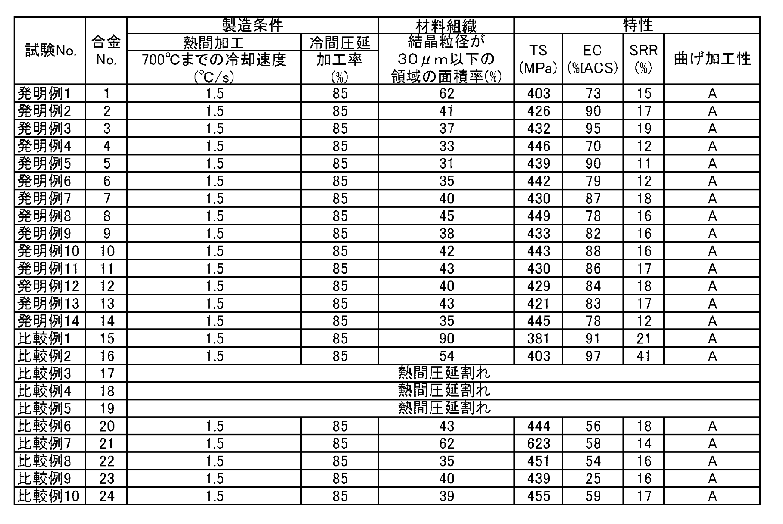
- Table 2 shows an invention example in which the production method is within the scope of the present invention and the component is also within the scope of the present invention, and a comparative example in which the component is outside the scope of the present invention.
- Inventive examples are all copper alloy materials having TS ⁇ 400 MPa, EC ⁇ 60% IACS, SRR ⁇ 20%, good bending workability, high conductivity, stress relaxation resistance, and good bending workability.
- any of strength, conductivity, stress relaxation resistance, and bending workability was inferior.
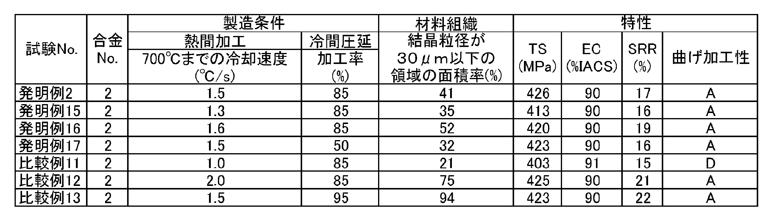
- Table 3 shows an invention example in which the alloy composition is within the scope of the present invention and a production method is also within the scope of the present invention, and a comparative example in which the production method is outside the scope of the present invention.
- Inventive examples are all copper alloy materials having TS ⁇ 400 MPa, EC ⁇ 60% IACS, SRR ⁇ 20%, good bending workability, high conductivity, stress relaxation resistance, and good bending workability.
- the comparative example whose manufacturing conditions are outside the scope of the present invention is inferior in either the stress relaxation resistance or the bending workability, and is insufficient as a material having a high target performance requirement.
- the copper alloy material within the scope of the present invention can have high conductivity, excellent stress relaxation resistance, and good bending workability, it is possible to combine in-vehicle components such as EV and HEV, peripheral infrastructure, and photovoltaic power generation. It is suitable for connectors such as systems, and other lead frames, relays, switches, sockets and the like.
Landscapes
- Chemical & Material Sciences (AREA)
- Engineering & Computer Science (AREA)
- Materials Engineering (AREA)
- Mechanical Engineering (AREA)
- Metallurgy (AREA)
- Organic Chemistry (AREA)
- Physics & Mathematics (AREA)
- Thermal Sciences (AREA)
- Crystallography & Structural Chemistry (AREA)
- Conductive Materials (AREA)
- Non-Insulated Conductors (AREA)
Abstract
Description
(1)Crを0.10~0.50質量%と、Mgを0.01~0.50質量%含み、Zr、Tiのうち少なくとも一種を合計で0.00~0.20質量%含有する第1添加元素群、およびZn、Fe、Sn、Ag、Si、Niのうち少なくとも一種を合計で0.00~0.50質量%含有する第2添加元素群からなる群から選ばれる一種を含有し、残部がCuと不可避的不純物からなる銅合金板材であって(ただし、上記Zr、Tiのうち少なくとも一種、およびZn、Fe、Sn、Ag、Si、Niのうち少なくとも一種からなる群から選ばれる一種は、いずれか1種以上を含有させてもよいし、いずれの種も含有させなくてもよい任意添加成分である。)、
板幅方向TDに垂直な断面において、粒径が30μm以下の結晶粒が30~70%の面積率を有することを特徴とする銅合金板材。
(2)Zr、Tiのうち少なくとも一種を合計で0.01~0.20質量%含有する第1添加元素群、およびZn、Fe、Sn、Ag、Si、Niのうち少なくとも一種を合計で0.01~0.50質量%含有する第2添加元素群からなる群から選ばれる少なくとも一種を含有する、(1)に記載の銅合金板材。
(3)材料表面への初期負荷応力を0.2%耐力の80%として、150℃中で1000時間放置した時の応力緩和率が20%以下であり、
90°W曲げした際にR/tが1.0で割れが発生しない、(1)または(2)に記載の銅合金板材。
(4)導電率が60%IACS以上である、(1)~(3)のいずれか1項に記載の銅合金板材。
(5)(1)~(4)のいずれか1項に記載の銅合金板材の製造方法であって、
(a)銅合金板材に相当する合金素材の溶解鋳造
(b)850~1050℃で均質加熱処理
(c)750℃以上で熱間加工を行い、熱間加工を終えた後、700℃まで1.3~1.6℃/秒で冷却
(d)90%以下の加工率で冷間加工
(e)350~650℃で10分~24時間の熱処理後、冷却速度2℃/分以下で300℃まで冷却、
(f)50%以下の加工率で仕上げ加工
(g)250~650℃で5秒~10時間の歪取り焼鈍
をこの順で有することを特徴とする、銅合金板材の製造方法。
(6)(1)~(4)のいずれか1項に記載の銅合金板材からなる電気電子部品。
本発明の上記及び他の特徴及び利点は、下記の記載からより明らかになるであろう。
本発明の銅合金材料は、加工組織と再結晶組織が入り混じった半軟化組織を有しており、板幅方向TDに垂直な断面(圧延方向RDと板厚方向NDからなる断面)を観察した際に、その断面において粒径が30μm以下の結晶が30~70%の面積率を有する。前記粒径の下限値には特に制限はないが、例えば1μm以上である。板幅方向TDは、圧延垂直方向ともいう。単に、板材の短手方向を指すものではなく、板材製造時の圧延方向RDに対して垂直であり、かつ板材の圧延面法線方向(板厚方向ND)に対しても垂直な方向が板幅方向TDである。
<Cr>
Crは、銅合金母相中に析出させることで、導電性を損なうことなく、強度と耐応力緩和特性を向上させることができる。本発明において、Crは0.10~0.50質量%、好ましくは0.15~0.40質量%、さらに好ましくは0.20~0.35質量%含まれる。Cr量が少なすぎると、銅母相中のCrまたはCrを含む化合物の量が少なくなるため、所望の強度、耐応力緩和特性が得られない。また熱処理工程において再結晶が過剰に進行し、上記の半軟化組織が得づらくなる。一方、多すぎると、導電性の低下、銅母相中における粗大な化合物の発生による強度の低下、曲げ加工性への悪影響といった問題が生じる。
Mgは、銅母相中に固溶元素として作用することで、強度と耐応力緩和特性を向上させることができる。本発明において、Mgは0.01~0.50質量%、好ましくは0.05~0.40質量%、さらに好ましくは0.10~0.30質量%含まれる。含有量が少なすぎると上記の各特性の改善効果が十分に得られない。また熱処理工程において再結晶が過剰に進行し、上記の半軟化組織が得づらくなる。一方、多すぎると、導電性の低下、加工性(例えば、熱間加工性)への悪影響といった問題が生じる。Mgは、銅母相中に固溶元素として作用することで耐応力緩和特性を向上させるため、PのようにMgと化合物を形成し析出させる元素を同時に添加することは、好ましくない。
本発明において、任意添加成分として添加できる、第1添加元素のTi、Zrは、銅母相中に析出させることで、強度と耐応力緩和特性を向上させることができる。本発明のこの態様において、Ti、Zrのうち少なくとも1種類を合計で0.01~0.20質量%、好ましくは0.05~0.15質量%、さらに好ましくは0.10~0.15質量%含有させても良い。含有量が少なすぎるとその添加の効果が十分でなく、多すぎると、導電性の低下、加工性(例えば、熱間加工性)への悪影響といった問題が生じる。
本発明の好ましい態様として、任意添加成分として、第2添加元素のZn、Fe、Sn、Ag、Si、Niを添加することで、強度、耐応力緩和特性、プレス性、めっき性といった材料特性を向上させることができる。この場合、Zn、Fe、Sn、Ag、Si、Niのうち少なくとも一種類を合計で0.01~0.50質量%、好ましくは0.05~0.40質量%、さらに好ましくは0.10~0.30質量%含有させても良い。含有量が少なすぎると、第2添加元素の添加の効果が十分でなく、多すぎると、導電性の低下、加工性(例えば、熱間加工性)への悪影響、原料費の増加といった問題が生じることがある。
次に、本発明の銅合金材料の製造方法の好ましい一例について説明する。
本発明の銅合金材料の通常の製造工程を示すと、a.溶解鋳造、b.均質化熱処理、c.熱間加工、d.冷間加工、e.熱処理、f.仕上げ加工、g.歪取り焼鈍を順に行なうことで製造される。さらに熱間加工後で冷間加工前に面削を行うことが好ましい。
この製造方法は、従来と同程度の工程数でありながら、それぞれの工程条件を適切に設定することで、目的の、材料特性の向上を実現できる。以下に詳述するように、本発明の製造方法においては、熱間加工後の冷却速度と冷間加工の加工率が重要であり、その後工程である仕上加工や歪取り焼鈍は、複数回実施しても良い。
Crを0.10~0.50質量%と、Mgを0.01~0.50質量%含み、残部がCuと不可避的不純物からなる銅合金素材を用意する。もしくは、Crを0.10~0.50質量%と、Mgを0.01~0.50質量%含み、Zr、Tiのうち少なくとも一種を合計で0.01~0.20質量%含有する第1添加元素群、およびZn、Fe、Sn、Ag、Si、Niのうち少なくとも一種を合計で0.01~0.50質量%含有する第2添加元素群からなる群から選ばれる少なくとも一種を含有し、残部がCuと不可避的不純物からなる銅合金素材を用意する。この銅合金素材を溶解炉により溶解鋳造を実施し、冷却して所定の成分を持つ鋳塊を得る。溶解鋳造は、通常の方法で行うことができる。
均質化熱処理は、鋳塊に含まれる化合物を銅母相中に固溶させ、鋳塊の成分を均質化するために実施する。これにより、添加した成分の効果を十分に得られるようになり、また材料中の特性のばらつきを小さくすることができる。本発明においては、好ましくは850~1050℃の温度で0.5~12時間、より好ましくは900~1050℃、さらに好ましくは950~1050℃で均質化熱処理を行う。
均質化熱処理した直後の鋳塊を熱間加工(熱間圧延など)して板厚を薄くする。熱間加工は750℃以上の温度で終了し、その後700℃まで1.3~1.6℃/sで冷却(例えば水冷)し、その後水冷する。熱間加工を高温で終了することで加工後の結晶粒径が大きくなり、さらに700℃までの冷却速度を遅くすることで結晶粒が成長するため、熱間圧延後に得られる材料の結晶粒径が所定の範囲に成長する。これにより、後工程である冷間加工で得られる加工組織の耐応力緩和特性が向上するだけでなく、熱処理工程において再結晶の起点となる結晶粒界が少なくなるため、目標とする半軟化組織が得易くなる。700℃までの冷却速度が遅すぎると、均質化熱処理により銅母相中に固溶させた添加元素が、冷却時に粗大な化合物として析出し、添加元素の効果を十分に得られなくなる。また冷却時に結晶粒が粗大に成長し、熱間圧延後に得られる材料の結晶粒径が所定の範囲より大きくなり、後工程である熱処理工程において、目標とする半軟化組織を得ることが難しくなる。また700℃までの冷却速度が速すぎると、冷却時に結晶粒が十分に成長せず、熱間圧延後に得られる材料の結晶粒径が所定の範囲より小さくなり、後工程である熱処理工程において、目標とする半軟化組織を得ることが難しくなる。
熱間加工後の材料表面に形成された酸化皮膜を面削により取り除く。面削工程は任意で行ってよい。面削は、公知の方法で行うことができる。
面削後の材料を、冷間加工(例えば冷間圧延)90%以下の加工率で行う。加工率は、好ましくは30~85%、さらに好ましくは加工率50~85%である。冷間加工の加工率が大きすぎる場合、後工程である熱処理工程において再結晶が進行しやすく、目標とする半軟化組織が得られなくなる。また冷間加工の加工率が小さすぎると、後工程である熱処理工程で再結晶が起こりづらくなる可能性があるため、好ましくは30%以上の加工率で冷間加工を行う。
冷間加工後の材料に対して、450~650℃で、10分~24時間の熱処理を行なう。熱処理により、加工組織の一部が再結晶し半軟化組織が得られるほか、銅母相中に微細な析出物が析出し、強度、導電性、耐応力緩和特性が向上する。低温で短時間処理する場合、熱処理時に再結晶が生じづらく、目標とする半軟化組織が得られないだけでなく、析出量が少なく、また析出する化合物の粒子径が微細すぎるため、強度、導電性、耐応力緩和特性の向上は望めない。また高温で長時間処理する場合、熱処理時に再結晶が過剰に進行し、目標とする半軟化組織が得られなくなるだけでなく、析出する化合物が粗大化し、導電性は向上するものの、強度、耐応力緩和特性の向上は望めない。また、時効熱処理後の300℃までの冷却速度は、≦2℃/分とすることが好ましい。300℃までの冷却速度をこの範囲とすることで、強度、導電性、耐応力緩和特性をより向上させることができる。
熱処理後の材料に、50%以下、より好ましくは10~40%の加工率で、仕上げ加工(仕上げ圧延など)を行なう。仕上げ加工により、強度が向上するが、導電性、耐応力緩和特性、曲げ加工性が低下する。仕上げ加工率が大きすぎる場合、導電性、耐応力緩和特性、曲げ加工性が著しく低下し、後の歪取り焼鈍工程で、これらの特性の回復と強度の維持を両立することが困難となる。
仕上げ加工後の材料に歪取り焼鈍を行なうことで、強度が低下するが、導電性、耐応力緩和特性、曲げ加工性が改善される。本発明では、250~650℃の温度で、5秒~10時間の歪取り焼鈍を行うのが好ましい。低温で短時間処理した場合、仕上げ加工で低下した導電性、耐応力緩和特性、曲げ加工性を回復できないことがある。またあまり高温で長時間処理すると、強度が著しく低下することがある。
金属顕微鏡により、材料の板幅方向TDに垂直な断面を観察(圧延方向RDと板厚方向NDからなる断面)し、結晶粒径が30μm以下の領域の面積率を算出した。観察は、熱処理工程後の材料について板幅方向TDに垂直な断面に湿式研磨およびバフ研磨を施し、クロム酸:水=1:1(容量比)の割合で混合した液にて数秒間研磨面を腐食した後、金属顕微鏡にて50~500倍の倍率で行った。また結晶粒径が30μm以下の領域の面積率については、次のようにして求めた。まず観察写真上、200μm×200μmの領域について、10μmのスパンで観察写真をます目状に区切り、結晶粒径が30μm以下の粒子が各ます目の半分以上の領域を満たす場合は、そのます目は結晶粒径が30μm以下の領域とみなした。その後、結晶粒径が30μm以下の領域とみなしたます目の総数を計数した。結晶粒径が30μm以下の領域とみなしたます目の総数を、観察したます目の総数で除して100をかけた値を、結晶粒径が30μm以下の領域の面積率とした。
圧延平行方向から切り出した試験片を、JIS Z2241に準じて3本測定し、その平均値を示した。TSが400MPa以上を合格とし、TSが400MPa未満を不合格とした。
20℃(±0.5℃)に保たれた恒温漕中で、四端子法により比抵抗を計測し、導電率を算出した。なお、端子間距離は100mmとした。
日本伸銅協会 JCBA T309:2004「銅及び銅合金薄板条の曲げによる応力緩和試験方法」に準じ、片持ちはり法(片持ちはりブロック式ジグ使用)により、材料表面への初期負荷応力を0.2%耐力の80%とし、150℃で1000時間保持の条件で測定した。試験片は幅10mmの短冊形とし、圧延平行方向と試験片の長さ方向を一致させた。応力緩和率の算出方法は、特許第5307305号に記載された算出方法による。すなわち、熱処理前、試験台に片持ちで保持した試験片に、耐力の80%の初期応力を付与した時の試験片の先端の位置は、基準位置から距離δ0の高さにある。これを150℃の恒温槽に1000時間保持(初期応力を付与した状態で上記試験片を熱処理)し、負荷を除いた後の試験片の先端の位置は、上記基準位置から距離Htの高さにある。また応力を負荷しなかった場合の試験片に対して上記の熱処理を行った場合の試験片の先端の位置は、上記基準位置から距離H1の高さにある。これらの関係から、応力緩和率(%)は(Ht-H1)/(δ0-H1)×100と算出した。
曲げ加工試験は、JIS Z 2248に準じて行った。材料を幅10mm、長さ50mmに切り出し、曲げ軸が圧延方向に垂直となるような90°W曲げ(GW:Good Way)、あるいは圧延方向に平行となるような90°W曲げ(BW:Bad Way)を実施した後、曲げ部表面を光学顕微鏡により200倍で観察し、割れの有無を調査した。曲げ加工性は、板厚をt、90°W曲げの内側曲げ半径をRとしたときに、R/tが1.0の条件でGWとBWの両方ともで割れが生じなかった場合を良好(A)、GWとBWのいずれか一方でも割れが生じた場合を劣(D)として判断した。

Claims (6)
- Crを0.10~0.50質量%と、Mgを0.01~0.50質量%含み、Zr、Tiのうち少なくとも一種を合計で0.00~0.20質量%含有する第1添加元素群、およびZn、Fe、Sn、Ag、Si、Niのうち少なくとも一種を合計で0.00~0.50質量%含有する第2添加元素群からなる群から選ばれる一種を含有し、残部がCuと不可避的不純物からなる銅合金板材であって(ただし、上記Zr、Tiのうち少なくとも一種、およびZn、Fe、Sn、Ag、Si、Niのうち少なくとも一種からなる群から選ばれる一種は、いずれか1種以上を含有させてもよいし、いずれの種も含有させなくてもよい任意添加成分である。)、
板幅方向TDに垂直な断面において、粒径が30μm以下の結晶粒が30~70%の面積率を有することを特徴とする銅合金板材。 - Zr、Tiのうち少なくとも一種を合計で0.01~0.20質量%含有する第1添加元素群、およびZn、Fe、Sn、Ag、Si、Niのうち少なくとも一種を合計で0.01~0.50質量%含有する第2添加元素群からなる群から選ばれる少なくとも一種を含有する、請求項1に記載の銅合金板材。
- 材料表面への初期負荷応力を0.2%耐力の80%として、150℃中で1000時間放置した時の応力緩和率が20%以下であり、
90°W曲げした際にR/tが1.0で割れが発生しない、請求項1または2に記載の銅合金板材。 - 導電率が60%IACS以上である、請求項1~3のいずれか1項に記載の銅合金板材。
- 請求項1~4のいずれか1項に記載の銅合金板材の製造方法であって、
(a)銅合金板材に相当する合金素材の溶解鋳造
(b)850~1050℃で均質加熱処理
(c)750℃以上で熱間加工を行い、熱間加工を終えた後、700℃まで1.3~1.6℃/秒で冷却
(d)90%以下の加工率で冷間加工
(e)350~650℃で10分~24時間の熱処理後、冷却速度2℃/分以下で300℃まで冷却、
(f)50%以下の加工率で仕上げ加工
(g)250~650℃で5秒~10時間の歪取り焼鈍
をこの順で有することを特徴とする、銅合金板材の製造方法。 - 請求項1~4のいずれか1項に記載の銅合金板材からなる電気電子部品。
Priority Applications (3)
| Application Number | Priority Date | Filing Date | Title |
|---|---|---|---|
| JP2015551901A JP6053959B2 (ja) | 2014-05-29 | 2015-05-29 | 銅合金板材及びその製造方法、前記銅合金板材からなる電気電子部品 |
| KR1020167033418A KR102441663B1 (ko) | 2014-05-29 | 2015-05-29 | 구리 합금 판재 및 그 제조 방법, 상기 구리 합금 판재로 이루어지는 전기전자 부품 |
| CN201580028078.7A CN106460095B (zh) | 2014-05-29 | 2015-05-29 | 铜合金板材及其制造方法、由所述铜合金板材构成的电气电子部件 |
Applications Claiming Priority (2)
| Application Number | Priority Date | Filing Date | Title |
|---|---|---|---|
| JP2014111771 | 2014-05-29 | ||
| JP2014-111771 | 2014-05-29 |
Publications (1)
| Publication Number | Publication Date |
|---|---|
| WO2015182777A1 true WO2015182777A1 (ja) | 2015-12-03 |
Family
ID=54699094
Family Applications (1)
| Application Number | Title | Priority Date | Filing Date |
|---|---|---|---|
| PCT/JP2015/065689 Ceased WO2015182777A1 (ja) | 2014-05-29 | 2015-05-29 | 銅合金板材及びその製造方法、前記銅合金板材からなる電気電子部品 |
Country Status (4)
| Country | Link |
|---|---|
| JP (1) | JP6053959B2 (ja) |
| KR (1) | KR102441663B1 (ja) |
| CN (1) | CN106460095B (ja) |
| WO (1) | WO2015182777A1 (ja) |
Cited By (2)
| Publication number | Priority date | Publication date | Assignee | Title |
|---|---|---|---|---|
| JP2019173043A (ja) * | 2018-03-26 | 2019-10-10 | 古河電気工業株式会社 | 銅合金条、その製造方法及びこれを用いたフラットケーブル |
| WO2024014173A1 (ja) * | 2022-07-14 | 2024-01-18 | Jx金属株式会社 | 圧延銅箔、銅張積層板、銅張積層板の製造方法、フレキシブルプリント配線板の製造方法及び電子部品の製造方法 |
Families Citing this family (7)
| Publication number | Priority date | Publication date | Assignee | Title |
|---|---|---|---|---|
| CN105950907A (zh) * | 2016-06-13 | 2016-09-21 | 芜湖卓越线束系统有限公司 | 高强度耐磨的线束端子用合金材料及其制备方法 |
| KR102489191B1 (ko) * | 2017-03-29 | 2023-01-16 | 후루카와 덴키 고교 가부시키가이샤 | 알루미늄 합금재 그리고 이것을 사용한 도전 부재, 전지용 부재, 체결 부품, 스프링용 부품 및 구조용 부품 |
| BE1025340B1 (de) * | 2017-06-30 | 2019-02-04 | Phoenix Contact Gmbh & Co. Kg | Verfahren zum Herstellen eines Kupfer aufweisenden Bauteils mittels selektivem Lasersinterm |
| EP3778944B1 (en) * | 2018-03-27 | 2024-09-25 | Furukawa Electric Co., Ltd. | Aluminum alloy material, and conductive member, battery member, fastening part, spring part, and structural part using aluminum alloy material |
| EP3778947B1 (en) * | 2018-03-27 | 2025-08-20 | Furukawa Electric Co., Ltd. | Aluminum alloy material, and conductive member, battery member, fastening part, spring part, and structural part using aluminum alloy material |
| CN112281023B (zh) * | 2020-11-23 | 2021-08-31 | 宁波博威合金材料股份有限公司 | 一种具有优异折弯性的铜合金材料及其制备方法和应用 |
| CN118305198A (zh) * | 2024-04-15 | 2024-07-09 | 太原晋西春雷铜业有限公司 | 一种太阳能光伏领域用c19210高性能铜带的短流程制备方法 |
Citations (3)
| Publication number | Priority date | Publication date | Assignee | Title |
|---|---|---|---|---|
| JPH0551671A (ja) * | 1991-08-21 | 1993-03-02 | Nikko Kyodo Co Ltd | 曲げ性及び応力緩和特性に優る電子機器用高力高導電性銅合金 |
| JP2012012644A (ja) * | 2010-06-30 | 2012-01-19 | Hitachi Cable Ltd | 銅合金の製造方法、及び銅合金 |
| JP2013129889A (ja) * | 2011-12-22 | 2013-07-04 | Furukawa Electric Co Ltd:The | 銅合金材およびその製造方法 |
Family Cites Families (3)
| Publication number | Priority date | Publication date | Assignee | Title |
|---|---|---|---|---|
| JP3731600B2 (ja) * | 2003-09-19 | 2006-01-05 | 住友金属工業株式会社 | 銅合金およびその製造方法 |
| EP2610359A4 (en) | 2010-08-27 | 2017-08-02 | Furukawa Electric Co., Ltd. | Copper alloy sheet and method for producing same |
| TWI571518B (zh) * | 2011-08-29 | 2017-02-21 | Furukawa Electric Co Ltd | Copper alloy material and manufacturing method thereof |
-
2015
- 2015-05-29 WO PCT/JP2015/065689 patent/WO2015182777A1/ja not_active Ceased
- 2015-05-29 KR KR1020167033418A patent/KR102441663B1/ko active Active
- 2015-05-29 JP JP2015551901A patent/JP6053959B2/ja active Active
- 2015-05-29 CN CN201580028078.7A patent/CN106460095B/zh active Active
Patent Citations (3)
| Publication number | Priority date | Publication date | Assignee | Title |
|---|---|---|---|---|
| JPH0551671A (ja) * | 1991-08-21 | 1993-03-02 | Nikko Kyodo Co Ltd | 曲げ性及び応力緩和特性に優る電子機器用高力高導電性銅合金 |
| JP2012012644A (ja) * | 2010-06-30 | 2012-01-19 | Hitachi Cable Ltd | 銅合金の製造方法、及び銅合金 |
| JP2013129889A (ja) * | 2011-12-22 | 2013-07-04 | Furukawa Electric Co Ltd:The | 銅合金材およびその製造方法 |
Cited By (2)
| Publication number | Priority date | Publication date | Assignee | Title |
|---|---|---|---|---|
| JP2019173043A (ja) * | 2018-03-26 | 2019-10-10 | 古河電気工業株式会社 | 銅合金条、その製造方法及びこれを用いたフラットケーブル |
| WO2024014173A1 (ja) * | 2022-07-14 | 2024-01-18 | Jx金属株式会社 | 圧延銅箔、銅張積層板、銅張積層板の製造方法、フレキシブルプリント配線板の製造方法及び電子部品の製造方法 |
Also Published As
| Publication number | Publication date |
|---|---|
| KR102441663B1 (ko) | 2022-09-13 |
| CN106460095A (zh) | 2017-02-22 |
| JP6053959B2 (ja) | 2016-12-27 |
| KR20170013881A (ko) | 2017-02-07 |
| JPWO2015182777A1 (ja) | 2017-04-20 |
| CN106460095B (zh) | 2018-10-16 |
Similar Documents
| Publication | Publication Date | Title |
|---|---|---|
| JP6053959B2 (ja) | 銅合金板材及びその製造方法、前記銅合金板材からなる電気電子部品 | |
| JP5224415B2 (ja) | 電気電子部品用銅合金材料とその製造方法 | |
| JP5391169B2 (ja) | 電気電子部品用銅合金材およびその製造方法 | |
| JP5476149B2 (ja) | 強度異方性が小さく曲げ加工性に優れた銅合金 | |
| JP4913902B2 (ja) | 電気・電子部品用銅合金材料の製造方法 | |
| JP5525247B2 (ja) | 高強度で曲げ加工性に優れた銅合金 | |
| JP5773929B2 (ja) | 曲げ加工性及び耐応力緩和特性に優れる電気電子部品用銅合金板 | |
| CN103080347A (zh) | 铜合金板材及其制造方法 | |
| JP5619389B2 (ja) | 銅合金材料 | |
| JP6265582B2 (ja) | 銅合金材およびその製造方法 | |
| JP2009007666A (ja) | 電気・電子機器用銅合金 | |
| WO2013018228A1 (ja) | 銅合金 | |
| CN102822364A (zh) | 电子材料用Cu-Ni-Si系合金 | |
| WO2010016428A1 (ja) | 電気・電子部品用銅合金材 | |
| JP2007291518A (ja) | Cu−Fe−P−Mg系銅合金および製造法並びに通電部品 | |
| JP5261161B2 (ja) | Ni−Si−Co系銅合金及びその製造方法 | |
| CN110506132A (zh) | Cu-Co-Si系铜合金板材和制造方法以及使用了该板材的部件 | |
| JP6133178B2 (ja) | 銅合金板材およびその製造方法 | |
| JP6301734B2 (ja) | 銅合金材及びその製造方法 | |
| JP4708497B1 (ja) | Cu−Co−Si系合金板及びその製造方法 | |
| JP2012229467A (ja) | 電子材料用Cu−Ni−Si系銅合金 | |
| CN118176312A (zh) | 电子材料用铜合金以及电子部件 | |
| CN106995890A (zh) | 电子部件用Cu‑Co‑Ni‑Si合金 | |
| JP2004353069A (ja) | 電子材料用銅合金 | |
| JP2025122511A (ja) | 銅合金板 |
Legal Events
| Date | Code | Title | Description |
|---|---|---|---|
| ENP | Entry into the national phase |
Ref document number: 2015551901 Country of ref document: JP Kind code of ref document: A |
|
| 121 | Ep: the epo has been informed by wipo that ep was designated in this application |
Ref document number: 15799803 Country of ref document: EP Kind code of ref document: A1 |
|
| ENP | Entry into the national phase |
Ref document number: 20167033418 Country of ref document: KR Kind code of ref document: A |
|
| NENP | Non-entry into the national phase |
Ref country code: DE |
|
| 122 | Ep: pct application non-entry in european phase |
Ref document number: 15799803 Country of ref document: EP Kind code of ref document: A1 |