WO2015174334A1 - ビームリード、半導体装置、および、半導体装置の製造方法 - Google Patents
ビームリード、半導体装置、および、半導体装置の製造方法 Download PDFInfo
- Publication number
- WO2015174334A1 WO2015174334A1 PCT/JP2015/063287 JP2015063287W WO2015174334A1 WO 2015174334 A1 WO2015174334 A1 WO 2015174334A1 JP 2015063287 W JP2015063287 W JP 2015063287W WO 2015174334 A1 WO2015174334 A1 WO 2015174334A1
- Authority
- WO
- WIPO (PCT)
- Prior art keywords
- beam lead
- semiconductor device
- chip
- electrical element
- joint
- Prior art date
- Legal status (The legal status is an assumption and is not a legal conclusion. Google has not performed a legal analysis and makes no representation as to the accuracy of the status listed.)
- Ceased
Links
Images





Classifications
-
- H—ELECTRICITY
- H10—SEMICONDUCTOR DEVICES; ELECTRIC SOLID-STATE DEVICES NOT OTHERWISE PROVIDED FOR
- H10W—GENERIC PACKAGES, INTERCONNECTIONS, CONNECTORS OR OTHER CONSTRUCTIONAL DETAILS OF DEVICES COVERED BY CLASS H10
- H10W72/00—Interconnections or connectors in packages
- H10W72/60—Strap connectors, e.g. thick copper clips for grounding of power devices
-
- H—ELECTRICITY
- H10—SEMICONDUCTOR DEVICES; ELECTRIC SOLID-STATE DEVICES NOT OTHERWISE PROVIDED FOR
- H10W—GENERIC PACKAGES, INTERCONNECTIONS, CONNECTORS OR OTHER CONSTRUCTIONAL DETAILS OF DEVICES COVERED BY CLASS H10
- H10W72/00—Interconnections or connectors in packages
- H10W72/071—Connecting or disconnecting
- H10W72/073—Connecting or disconnecting of die-attach connectors
- H10W72/07331—Connecting techniques
- H10W72/07336—Soldering or alloying
-
- H—ELECTRICITY
- H10—SEMICONDUCTOR DEVICES; ELECTRIC SOLID-STATE DEVICES NOT OTHERWISE PROVIDED FOR
- H10W—GENERIC PACKAGES, INTERCONNECTIONS, CONNECTORS OR OTHER CONSTRUCTIONAL DETAILS OF DEVICES COVERED BY CLASS H10
- H10W72/00—Interconnections or connectors in packages
- H10W72/071—Connecting or disconnecting
- H10W72/076—Connecting or disconnecting of strap connectors
- H10W72/07631—Techniques
- H10W72/07637—Techniques using a polymer adhesive, e.g. an adhesive based on silicone or epoxy
-
- H—ELECTRICITY
- H10—SEMICONDUCTOR DEVICES; ELECTRIC SOLID-STATE DEVICES NOT OTHERWISE PROVIDED FOR
- H10W—GENERIC PACKAGES, INTERCONNECTIONS, CONNECTORS OR OTHER CONSTRUCTIONAL DETAILS OF DEVICES COVERED BY CLASS H10
- H10W72/00—Interconnections or connectors in packages
- H10W72/071—Connecting or disconnecting
- H10W72/076—Connecting or disconnecting of strap connectors
- H10W72/07651—Connecting or disconnecting of strap connectors characterised by changes in properties of the strap connectors during connecting
- H10W72/07653—Connecting or disconnecting of strap connectors characterised by changes in properties of the strap connectors during connecting changes in shapes
-
- H—ELECTRICITY
- H10—SEMICONDUCTOR DEVICES; ELECTRIC SOLID-STATE DEVICES NOT OTHERWISE PROVIDED FOR
- H10W—GENERIC PACKAGES, INTERCONNECTIONS, CONNECTORS OR OTHER CONSTRUCTIONAL DETAILS OF DEVICES COVERED BY CLASS H10
- H10W72/00—Interconnections or connectors in packages
- H10W72/60—Strap connectors, e.g. thick copper clips for grounding of power devices
- H10W72/651—Materials of strap connectors
- H10W72/652—Materials of strap connectors comprising metals or metalloids, e.g. silver
-
- H—ELECTRICITY
- H10—SEMICONDUCTOR DEVICES; ELECTRIC SOLID-STATE DEVICES NOT OTHERWISE PROVIDED FOR
- H10W—GENERIC PACKAGES, INTERCONNECTIONS, CONNECTORS OR OTHER CONSTRUCTIONAL DETAILS OF DEVICES COVERED BY CLASS H10
- H10W90/00—Package configurations
- H10W90/701—Package configurations characterised by the relative positions of pads or connectors relative to package parts
- H10W90/761—Package configurations characterised by the relative positions of pads or connectors relative to package parts of strap connectors
- H10W90/764—Package configurations characterised by the relative positions of pads or connectors relative to package parts of strap connectors between a chip and a stacked insulating package substrate, interposer or RDL
Definitions
- the present invention relates to a beam lead, a semiconductor device, and a method for manufacturing the semiconductor device.
- the beam lead is formed by bending a long metal plate made of copper, aluminum or the like. Specifically, chip-side joints and circuit-side joints are provided at both ends of the beam lead in the longitudinal direction, and these chip-side joints and circuit-side joints are joined together via a rising part and a crossing part. ing.
- the chip side joint is joined to a semiconductor chip (electrical element) via solder, and the circuit side joint is joined to the circuit layer on the substrate via solder.
- the beam lead disclosed in Japanese Patent Application Laid-Open No. 2010-50364 has high rigidity because it is formed by bending a metal plate. Therefore, if the beam lead expands or contracts (deforms) due to temperature change, stress is applied to the solder part at the chip side joint or the circuit side joint, and the solder part may be damaged if it deteriorates with age over a long period of use. There is sex.
- the present invention has been made in view of the above problems, and a beam lead and a semiconductor device capable of reducing stress input to a joint portion between the beam lead and an electrical element when the temperature of the beam lead changes. And it aims at providing the manufacturing method of a semiconductor device.
- the beam lead according to the present invention has a net-like member made of a flexible mesh or a braid, and is connected to an electrical element on the substrate.
- the beam lead may include the mesh member and a reinforcing material provided along the mesh member.
- a semiconductor device includes a substrate made of an insulating material, an electrical element disposed on the substrate, and the beam lead joined to the electrical element,
- the beam lead has a joint portion that is joined to the electrical element by solder, and after squeezing at least a part of the joint portion, the joint portion is joined to the electrical element by solder.
- the beam lead in the semiconductor device includes the joining portion and a connecting portion connected to the joining portion, and after crushing the boundary portion between the joining portion and the joining portion in the connecting portion, the solder The joining portion may be joined to the electrical element.
- the beam lead in the semiconductor device may be joined to the electrical element by sintering.
- a method for manufacturing a semiconductor device includes: Applying a sintered paste to at least one of a beam lead having an elastic mesh or a braided mesh member and an electrical element; Abutting the beam lead to an electrical element via a sintered paste; By heating the contact portion, the step of joining the beam lead to the electrical element with the metal particles in the sintered paste, Have
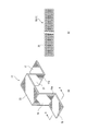
- FIG. 1 is a perspective view showing the semiconductor device according to the first embodiment.
- 2A is a perspective view showing the beam lead in FIG. 1
- FIG. 2B is a cross-sectional view taken along the line AA in FIG. 2A.
- FIG. 3 shows an example of the present invention
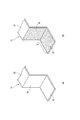
- FIG. 3 (a) is a perspective view showing a crushing range in the beam lead of FIG. 2
- FIG. 3 (b) is a perspective view showing a beam lead with soldered joints. is there.
- FIG. 4 shows a comparative example with FIG. 3, and FIG. 4 (a) is a perspective view showing a state in which the joint and the connecting part are not crushed before soldering the joint in the beam lead, and FIG. 4 (b).
- FIG. 3 shows an example of the present invention
- FIG. 3 (a) is a perspective view showing a crushing range in the beam lead of FIG. 2
- FIG. 3 (b) is a perspective view showing a beam lead with soldered joints. is there.
- FIG. 4
- FIG. 3 is a perspective view showing a beam lead soldered to a joint without crushing the joint and the connecting part.
- FIG. 5 shows a procedure for joining the beam lead according to the second embodiment to a semiconductor chip
- FIG. 5 (a) is a side view showing the semiconductor chip
- FIG. 5 (b) is a paste paste on the semiconductor chip.
- FIG. 5C is a side view showing a state in which the joint portion of the beam lead is placed on the sintered paste
- FIG. 5C shows the beam lead with the metal particles in the paste by heating the joint portion of the beam lead. It is a side view which shows the state which joins this junction part and a semiconductor chip.
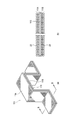
- FIG. 6 is an exploded perspective view of the beam lead according to the third embodiment. 7 shows the beam lead of FIG. 6, FIG.
- FIG. 7 (a) is a perspective view of the beam lead
- FIG. 7 (b) is a sectional view taken along line BB of FIG. 7 (a).
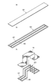
- FIG. 8 shows a beam lead according to the fourth embodiment.
- FIG. 8 (a) is a perspective view showing a rectangular steel plate as a reinforcing material
- FIG. 8 (b) is a steel plate of FIG. 8 (a).
- FIG. 8C is a perspective view showing a beam lead disposed on the back side of the mesh member by bending the frame body shown in FIG. 8B. It is.
- FIG. 9 is a perspective view showing a beam lead according to a modification of the fourth embodiment.
- the side where the semiconductor chip is mounted in the longitudinal direction of the beam lead is the front side FR
- the opposite side of the front side FR is the rear side RR
- the front side is the front side.
- the right side is RH and the left side is LH.
- the semiconductor device 1 includes a substrate 3 made of an insulating material, and a plurality (two in FIG. 1) of first and second substrates disposed on the substrate 3.
- a plate-like beam lead 11 for connecting the upper surfaces 7a and 9a.
- FIG. 1 only one semiconductor chip 7, first on-substrate circuit layer 5, second on-substrate circuit layer 9, and beam lead 11 are illustrated, but a plurality of these may be provided. Good.
- the semiconductor chip 7 is bonded to the upper surface of the first on-substrate circuit layer 5 via solder S.
- the semiconductor chip 7 is illustrated in the first embodiment, but the electric element is not limited thereto.
- the beam lead 11 is arranged on the lower side and is arranged at a predetermined interval in the front-rear direction and a chip side joint 15 (joint) and a circuit layer side joint.
- the bridging portion 23 (connecting portion) that connects each other and the side view are integrally formed in a hat shape.
- the chip-side joint 15 (joint) and the circuit layer-side joint 17 are joined to the semiconductor chip 7 and the second on-substrate circuit layer 9 via solder S, respectively.
- the entire beam lead 11 is composed of a mesh member made of a flexible braid.
- the braid is a braid formed by knitting a plurality of thin linear bodies 25, and can be freely deformed when a load is applied. Have sex. That is, the shape of the beam lead 11 can be freely deformed only by applying a small load.
- a boundary portion 27 is formed between the chip-side joint portion 15 (joint portion) and the standing wall portion 19 (connecting portion). That is, the boundary portion 27 includes a lower end portion of the standing wall portion 19 and an end portion on the standing wall portion 19 side in the chip side joint portion 15.
- the entire chip side bonding portion 15 (bonding portion) and the connecting portion 27 are crushed.
- the crushing range P is indicated by line hatching as shown in FIG.
- the chip-side joining portion 15 and the connecting portion 27 are crushed in the thickness direction, the gap between the linear bodies 25 constituting the beam lead 11 is significantly reduced. This crushing process is performed in advance with the beam lead alone before the soldering process.
- the crushed chip side joint 15 is joined to the upper surface 7a of the semiconductor chip 7 (electrical element) with solder S.
- the chip-side joint 15 is placed on the upper surface 7 a of the semiconductor chip 7 (electrical element) with solder S without crushing the chip-side joint 15 and the connecting portion 27. Join.
- FIG. 3 and FIG. 4 are compared.
- the range P is crushed and the gap between the linear bodies 25 is crushed and then soldered, so as shown in FIG. It is possible to suppress the solder S from being sucked up (permeated) more than necessary into the side joint portion 15 and the connecting portion 27. Therefore, a solder layer is formed with an appropriate thickness between the lower surface of the chip-side bonding portion 15 and the upper surface 7a of the semiconductor chip 7. Therefore, the lower surface of the chip-side bonding portion 15 and the upper surface 7a of the semiconductor chip 7 can be efficiently bonded via the solder layer.
- FIG. 4 according to the comparative example, as shown in FIG. 4A, the chip-side joint 15 and the connecting portion 27 are not crushed before the soldering process.
- the gap between the linear bodies 25 is large. Accordingly, as shown in FIG. 4B, within the range indicated by the point hatching S, the solder S gradually invades into the gaps between the linear bodies 25 by the capillary phenomenon, and the lower surface of the chip-side joint 15 and the semiconductor It becomes difficult to ensure an appropriate thickness for the solder layer formed between the upper surface 7a of the chip 7. Therefore, it becomes difficult to efficiently join the lower surface of the chip-side bonding portion 15 and the upper surface 7a of the semiconductor chip 7 via the solder layer.
- the beam lead 11 according to the first embodiment is connected to a semiconductor chip 7 (electrical element) disposed on the substrate 3 and is composed of a mesh member made of a flexible braid. .
- the beam lead 11 according to the present embodiment is composed of a mesh member made of a braid having flexibility, the rigidity is lower than that of a conventional beam lead made of a conventional metal. For this reason, even if the temperature of the beam lead 11 changes, the stress input to the joint between the beam lead 11 and the electrical element 7 is reduced, and the joint between the beam lead 11 and the electrical element 7 is damaged. Is effectively suppressed.
- the semiconductor device 1 is connected to the substrate 3 made of an insulating material, the semiconductor chip 7 (electrical element) disposed on the substrate 3, and the semiconductor chip 7 and has flexibility.
- a beam lead 11 composed of a net-like member made of a braid.
- the chip-side joint 15 (joint) of the beam lead 11 is joined to the semiconductor chip 7 with solder S.
- the chip side joint 15 of the beam lead 11 is formed by being crushed at least partially and then joined to the semiconductor chip 7 (electrical element) with solder S.
- the gap between the linear bodies 25 is large in the chip side joint 15 and the connecting part 27. Yes. Therefore, the capillary phenomenon causes the solder S to permeate more and more than necessary into the gaps between the linear bodies 25, and the appropriate solder layer formed between the lower surface of the chip-side joint 15 and the upper surface 7 a of the semiconductor chip 7. It is difficult to ensure a sufficient thickness. Therefore, it is difficult to efficiently join the lower surface of the chip-side bonding portion 15 and the upper surface 7a of the semiconductor chip 7.
- the beam lead 11 includes a chip-side bonding portion 15 (bonding portion) bonded to the semiconductor chip 7 and connecting portions 19, 21, 23 connected to the chip-side bonding portion 15 (bonding portion). Yes. After crushing the boundary portion 27 of the connecting portion with the joint portion and the joint portion 15, the chip-side joint portion 15 is joined to the semiconductor chip 7 with the solder S.
- the gap between the linear bodies 25 constituting the braid of the standing wall portion 19 and the chip side joint portion 15 as the connecting portion is crushed.
- the connecting portion is not crushed, the solder S may be sucked (permeated) to the upper end of the standing wall portion 19 as shown in FIG. Therefore, the chip-side joining portion 15 and the boundary portion 27 are also crushed to suppress the solder S from being sucked up to the standing wall portion 19. That is, as shown in FIG. 3B, the range in which the solder S is sucked up is limited to the lower end of the standing wall 19.
- solder layer having a more appropriate thickness is formed between the lower surface of the chip-side bonding portion 15 and the upper surface 7a of the semiconductor chip 7, the lower surface of the chip-side bonding portion 15 and the upper surface 7a of the semiconductor chip 7 are connected. Furthermore, it can join efficiently.
- the chip-side bonding portion 15 (bonding portion) and the circuit layer-side bonding portion 17 are bonded to the semiconductor chip 7 and the second substrate circuit layer 9 by sintering. Yes.
- the bonding procedure will be specifically described with the chip side bonding portion 15 as an example.
- a paste 31 is applied on the upper surface 7 a of the semiconductor chip 7. Then, the chip-side bonding portion 15 is placed on and in contact with the sintering paste 31. Thereafter, when the vicinity of the chip-side bonding portion 15 is heated, the chip-side bonding portion 15 is made to be a semiconductor chip by metal particles 33 (for example, silver particles) in the sintering paste 31 as shown in FIG. 7 is joined.
- metal particles 33 for example, silver particles
- a semiconductor device is connected to a substrate 3 made of an insulating material, a semiconductor chip 7 (electrical element) disposed on the substrate 3, and the semiconductor chip 7. And a beam lead 11 composed of a mesh member made of a braid having flexibility.
- the chip-side joint 15 (joint) of the beam lead 11 is joined to the semiconductor chip 7 by sintering.
- the chip-side joint 15 of the beam lead 11 is less likely to be displaced laterally with respect to the semiconductor chip 7 without pressing the chip-side joint 15 of the beam lead 11 against the semiconductor chip 7 at the time of sintering. That is, as described above, the beam lead 11 is composed of a braid having flexibility, so that the rigidity is lowered. Therefore, when the shape of the beam lead 11 changes due to heat at the time of sintering, the stress at which the chip-side joint 15 is deformed in the lateral direction is reduced, so that the chip-side joint 15 is not easily displaced in the lateral direction.
- the rigidity of the beam lead 11 is reduced, when the shape of the beam lead 11 changes due to heat during sintering, the stress that deforms the chip-side bonding portion 15 in the lateral direction is reduced. The portion 15 is less likely to be displaced in the lateral direction.
- the beam lead according to the third embodiment has a three-layer structure. Specifically, as shown in FIGS. 6 and 7, a second component member (net-like member) 11B disposed on the lower side and a third component member (reinforcing material) disposed on the upper side of the second component member 11B. ) 113 and a first component member (mesh member) 11A disposed on the upper side of the third component member 113.
- the first component member 11A, the second component member 11B, and the third component member 113 are each formed in a hat shape when viewed from the side.
- the first component member 11 ⁇ / b> A and the second component member 11 ⁇ / b> B are braided mesh members. Moreover, the 3rd structural member 113 arrange
- the beam lead 111 is configured by joining the first component member 11A, the second component member 11B, and the third component member 113 together and integrating them.
- the third component member 113 is provided along the first component member 11A and the second component member 11B.
- a beam lead 111 according to the third embodiment is sandwiched between a first constituent member 11A and a second constituent member 11B made of a braid, and the first constituent member 11A and the second constituent member 11B. And a third component member 113 made of copper foil (metal foil). The first component member 11A, the second component member 11B, and the third component member 113 are joined together and formed integrally.
- the third component member 113 is made of a metal foil (reinforcing material), the third component member 113 has an effect that the strength is improved as compared with a beam lead composed of only a braid having flexibility.
- This strength is the minimum necessary strength required for the beam lead (for example, strength that allows efficient processing, strength that does not deform during use of the beam lead, etc.).
- a frame-like body obtained by punching the inner side of a steel plate is used as the reinforcing material. This will be specifically described below.
- the steel plate 201 is a flat plate formed in a rectangular shape in plan view.
- the inner side of the steel plate 201 is punched out with a press along a longitudinal direction.
- punching is performed so that the pair of belt-like bodies come out in parallel in the short direction.
- the frame-like body 203 which is a reinforcing material having a strength of a predetermined value or more is completed. Therefore, openings 205 and 207 extending in the longitudinal direction are arranged in parallel with the frame-like body 203.
- a thickness of the steel plate 201 of 0.3 mm to 0.5 mm can be applied.
- the frame-shaped body 203 of FIG.8 (b) is bend
- the beam lead 211 according to the present embodiment is created by placing the mesh member on the folded steel plate frame 203.
- the frame-like body 203 and the first component member 11A are not joined, but are merely brought into contact with each other.
- a beam lead 211 according to the fourth embodiment includes a first component member 11A (mesh-like member) and a frame-like body 203 (reinforcing material) provided along the first component member 11A.
- the beam lead 211 since the beam lead 211 includes the frame-like body 203 that is a reinforcing material, the beam lead 211 has an effect that the strength is improved as compared with the beam lead that is formed only of a flexible braid. This strength is the minimum necessary strength required for the beam lead (for example, strength that allows efficient processing, strength that does not deform during use of the beam lead, etc.).
- the beam lead 11, the first component member 11A, and the second component member 11B are configured by braiding, but may be configured by a flexible metal (for example, copper) mesh.
- the copper foil is taken as an example of the metal foil constituting the third component 113, but other than the copper foil may be used.
- the sintered paste 31 is applied to the semiconductor chip 7, but it may be applied to the beam lead 11.
- a frame-like body may be sandwiched between a pair of mesh members to form a beam lead.
- first component member 11A and a second component member 11B according to the third embodiment are prepared.
- the first component member 11 ⁇ / b> A and the second component member 11 ⁇ / b> B are configured by a mesh member formed of a braid.
- a frame-like body 203 (reinforcing material) according to the fourth embodiment is prepared.
- the beam lead 311 may be created. Also in this case, since the beam lead 311 includes the frame-like body 203 that is a reinforcing material, the beam lead 311 has an effect that the strength is improved as compared with the beam lead that is configured only by a braid having flexibility.
Landscapes
- Die Bonding (AREA)
Abstract
本発明に係るビームリードは、基板の上に配設される半導体チップに接続され、可撓性を有するメッシュまたは編組からなる網状部材を有する。ビームリードは、可撓性を有するため、従来の金属よりも剛性が低い。このため、ビームリードの温度が変化して形状が変化しても、ビームリードと半導体チップとの接合部分に入力される応力が低減する。
Description
本発明は、ビームリード、半導体装置、および、半導体装置の製造方法に関する。
従来から、ハイブリッド車や電気自動車等の車両に搭載される半導体装置の開発が進められている(日本国 特開2010-50364号公報を参照)。
この日本国 特開2010-50364号公報に記載された半導体装置においては、絶縁基板上に設けられた半導体チップと基板上回路層とを、ビームリードを介して接続している。
前記ビームリードは、銅やアルミニウム等からなる長尺状の金属板を折り曲げて成形される。具体的には、ビームリードにおける長手方向の両端にチップ側接合部および回路側接合部を設け、これらのチップ側接合部および回路側接合部同士を立ち上がり部および渡り部を介して一体に結合している。前記チップ側接合部を半導体チップ(電気的素子)にはんだを介して接合すると共に、前記回路側接合部を基板上回路層にはんだを介して接合している。
しかしながら、日本国 特開2010-50364号公報に開示されたビームリードは、金属板を折り曲げて成形されているため、剛性が高い。従って、ビームリードが温度変化によって伸縮(変形)すると、チップ側接合部や回路側接合部におけるはんだ部分に応力がかかり、長期間の使用で経年劣化すると、前記はんだ部分が損傷する要因になる可能性がある。
本発明は、前記課題に鑑みてなされたものであり、ビームリードが温度変化したときに、ビームリードと電気的素子との接合部分に入力される応力を低減させることができるビームリード、半導体装置、および、半導体装置の製造方法を提供することを目的とする。
前記目的を達成するため、本発明に係るビームリードは、可撓性を有するメッシュまたは編組からなる網状部材を有し、基板上の電気的素子に接続される。
前記ビームリードは、前記網状部材と、前記網状部材に沿って設けられた補強材と、を有してもよい。
また、本発明に係る半導体装置は、絶縁材料で構成された基板と、該基板の上に配設された電気的素子と、該電気的素子に接合された前記ビームリードと、を備え、前記ビームリードは、前記電気的素子にはんだで接合される接合部を有し、前記接合部の少なくとも一部を押し潰した後で、接合部をはんだで電気的素子に接合する。
前記半導体装置におけるビームリードは、前記接合部と、該接合部に繋がる連結部と、を備え、前記連結部における接合部との境界部と、前記接合部と、を押し潰した後で、はんだで接合部を電気的素子に接合してもよい。
前記半導体装置におけるビームリードは、前記電気的素子にシンタ接合によって接合されてもよい。
本発明に係る半導体装置の製造方法は、
可撓性を有するメッシュまたは編組からなる網状部材を有するビームリードと電気的素子との少なくともいずれかにシンタペーストを塗布する工程と、
前記ビームリードを、シンタペーストを介して電気的素子に当接する工程と、
この当接部を加熱することにより、シンタペースト中の金属粒子でビームリードを電気的素子に接合させる工程と、
を有する。
可撓性を有するメッシュまたは編組からなる網状部材を有するビームリードと電気的素子との少なくともいずれかにシンタペーストを塗布する工程と、
前記ビームリードを、シンタペーストを介して電気的素子に当接する工程と、
この当接部を加熱することにより、シンタペースト中の金属粒子でビームリードを電気的素子に接合させる工程と、
を有する。
以下、本発明の一例としての実施形態を図面に基づいて詳細に説明する。なお、以下の図において、構成を判りやすく説明するために、便宜上、ビームリードの長手方向のうち半導体チップが実装された側を前側FR、前側FRの反対側を後側RR、前側に向かって右側をRH、左側をLHとする。
[第1の実施形態]
図1~図3を参照して、本発明の第1の実施形態に係る半導体装置およびビームリードについて説明する。
図1~図3を参照して、本発明の第1の実施形態に係る半導体装置およびビームリードについて説明する。
図1に示すように、第1の実施形態に係る半導体装置1は、絶縁材料で構成される基板3と、該基板3上に配設される複数(図1では2つ)の第1および第2の基板上回路層5,9と、第1の基板上回路層5の上に接合される半導体チップ7(電気的素子)と、該半導体チップ7および第2の基板上回路層9の上面同士7a,9aを接続する板状のビームリード11と、を備えている。なお、図1では、半導体チップ7、第1の基板上回路層5、第2の基板上回路層9、および、ビームリード11を1つずつしか記載していないが、これらを複数設けてもよい。前記半導体チップ7は、はんだSを介して第1の基板上回路層5の上面に接合されている。また、「電気的素子」として、第1の実施形態では、半導体チップ7を例示するが、電気的素子は、これらに限定されない。
次いで、図1,2を用いて、第1の実施形態に係るビームリード11について説明する。
図1および図2(a)に示すように、このビームリード11は、下側に配置されて前後方向に所定間隔をおいて配置されたチップ側接合部15(接合部)および回路層側接合部17と、これらのチップ側接合部15および回路層側接合部17における端縁15a,17aから屈曲して上側に延びる立壁部19,21(連結部)と、該立壁部19,21における上端同士を結ぶ橋渡し部23(連結部)と、から側面視がハット状に一体形成されている。チップ側接合部15(接合部)および回路層側接合部17は、それぞれ半導体チップ7および第2の基板上回路層9にはんだSを介して接合されている。
また、ビームリード11の全体は、可撓性を有する編組からなる網状部材で構成されている。具体的には、図2(b)に示すように、編組とは、複数の細い線状体25を細かく組み合わせて編んだものであり、荷重を加えると自由に変形が可能であり、可撓性を有する。即ち、小さい荷重を加えるだけで、ビームリード11の形状を自由に変形させることが可能である。
次に、図3と図4を用いて、ビームリード11のチップ側接合部15の全面と連結部27とを押し潰した後で、チップ側接合部15をはんだSで接合する場合と、ビームリード11のどの部位も全く押し潰さないで接合する場合と、を比較する。
まず、図3(a)に示すように、ビームリード11では、チップ側接合部15(接合部)と立壁部19(連結部)との間が境界部27に形成されている。つまり、境界部27は、立壁部19の下端部と、チップ側接合部15における立壁部19側の端部とからなる。本発明例では、図3(a)に示すように、チップ側接合部15(接合部)の全体と、連結部27と、を押し潰す。なお、押し潰す範囲Pは、図3(a)に示すように、線ハッチングで示している。ここで、チップ側接合部15および連結部27を厚さ方向に押し潰すと、ビームリード11を構成する線状体25同士の隙間が大幅に減少する。なお、この押し潰し加工は、はんだ付け工程の前にビームリード単体で予め行なっておく。
次に、図3(b)に示すように、この押し潰したチップ側接合部15を半導体チップ7(電気的素子)の上面7aにはんだSで接合する。
一方、図4に示すように、比較例では、チップ側接合部15と連結部27とを押し潰さないまま、チップ側接合部15を半導体チップ7(電気的素子)の上面7aにはんだSで接合する。
以下に、図3と図4を比較する。
本発明例では、図3(a)に示すように、前記範囲Pを押し潰して線状体25同士の隙間を潰した後ではんだ接合するため、図3(b)に示すように、チップ側接合部15および連結部27にはんだSが必要以上に吸い上げられる(浸透する)ことが抑制される。従って、チップ側接合部15の下面と半導体チップ7の上面7aとの間に、はんだ層が適正な厚さをもって形成される。よって、チップ側接合部15の下面と半導体チップ7の上面7aとをはんだ層を介して効率的に接合することができる。
比較例に係る図4では、図4(a)に示すように、はんだ付け工程の前にチップ側接合部15および連結部27を押し潰していないため、チップ側接合部15および連結部27において線状体25同士の隙間が大きい。従って、図4(b)に示すように、点ハッチングSで示す範囲で、毛細管現象によって前記線状体25同士の隙間にはんだSがどんどん浸入してしまい、チップ側接合部15の下面と半導体チップ7の上面7aとの間に形成されるはんだ層について適正な厚さを確保することが困難になる。従って、チップ側接合部15の下面と半導体チップ7の上面7aとをはんだ層を介して効率的に接合することが困難になる。
以下に、第1の実施形態による作用効果を説明する。
(1)第1の実施形態に係るビームリード11は、基板3の上に配設される半導体チップ7(電気的素子)に接続され、可撓性を有する編組からなる網状部材で構成される。
本実施形態に係るビームリード11が、可撓性を有する編組からなる網状部材で構成されるため、従来の金属からなる従来のビームリードよりも剛性が低い。このため、ビームリード11の温度が変化しても、ビームリード11と電気的素子7との接合部分に入力される応力が低減し、ビームリード11と電気的素子7との接合部分が損傷することが効果的に抑制される。
また、ビームリード11に高周波電流を流す場合、表皮効果によって、ビームリード11を構成するそれぞれの線状体25における表面部分を高周波電流が集中的に流れる。従って、複数の線状体が絡み合って構成されるビームリード全体では、ビームリード11の断面の全体に分散して高周波電流が流れるため、ノイズが効率的に低減される。なお、これに対して、従来の金属板からなるビームリードでは、電流密度が金属板の表面部分で高くなり高周波電流が流れにくくなるため、ノイズの発生量が大きくなる。
(2)半導体装置1は、絶縁材料で構成される基板3と、該基板3の上に配設される半導体チップ7(電気的素子)と、半導体チップ7に接続されると共に可撓性を有する編組からなる網状部材で構成されたビームリード11と、を備える。前記ビームリード11のチップ側接合部15(接合部)は、半導体チップ7にはんだSで接合される。前記ビームリード11のチップ側接合部15は、少なくとも一部を押し潰した後で、はんだSで半導体チップ7(電気的素子)に接合されてなる。
この押し潰し加工によって、チップ側接合部15の編組を構成する線状体25同士の隙間が潰れるため、線状体25同士の隙間に必要以上にはんだSが吸い上げられる(浸透する)ことが抑制される。従って、チップ側接合部15の下面と半導体チップ7の上面7aとの間に適正な厚さのはんだ層が形成されるため、チップ側接合部15の下面と半導体チップ7の上面7aとを効率的に接合することができる。
これに対して、はんだ付け工程の前でチップ側接合部15および連結部27を押し潰さない場合は、チップ側接合部15および連結部27において線状体25同士の隙間が大きい状態になっている。従って、毛細管現象によって線状体25同士の隙間にはんだSが必要以上にどんどん浸透してしまい、チップ側接合部15の下面と半導体チップ7の上面7aとの間に形成されるはんだ層の適正な厚さを確保することが困難になる。従って、チップ側接合部15の下面と半導体チップ7の上面7aとを効率的に接合することが困難になる。
(3)前記ビームリード11は、半導体チップ7に接合されるチップ側接合部15(接合部)と、チップ側接合部15(接合部)に繋がる連結部19,21,23と、を備えている。前記連結部における接合部との境界部27と、前記接合部15と、を押し潰した後で、はんだSでチップ側接合部15を半導体チップ7に接合してなる。
チップ側接合部15のみならず境界部27も押し潰しているため、連結部である立壁部19とチップ側接合部15の編組を構成する線状体25同士の隙間が潰れる。ここで、連結部を押し潰さないと、図4(b)のように、立壁部19の上端まではんだSが吸い上げられる(浸透する)おそれがある。よって、チップ側接合部15および境界部27も押し潰すことにより、立壁部19まではんだSが吸い上げられることが抑制される。即ち、図3(b)に示すように、はんだSが吸い上げられる範囲は、立壁部19の下端部までに限定される。従って、チップ側接合部15の下面と半導体チップ7の上面7aとの間にさらに適正な厚さのはんだ層が形成されるため、チップ側接合部15の下面と半導体チップ7の上面7aとをさらに効率的に接合することができる。
[第2の実施形態]
次いで、第2の実施形態に係る半導体装置およびビームリードについて説明する。ただし、前述した第1の実施形態と同一構成については、同一の符号を付けて説明を省略する。
次いで、第2の実施形態に係る半導体装置およびビームリードについて説明する。ただし、前述した第1の実施形態と同一構成については、同一の符号を付けて説明を省略する。
第2の実施形態に係る半導体装置においては、チップ側接合部15(接合部)および回路層側接合部17は、それぞれ半導体チップ7および第2の基板上回路層9にシンタ接合によって接合されている。以下、チップ側接合部15を例にとって具体的に接合の手順を説明する。
図5(a)(b)に示すように、まず、半導体チップ7の上面7aの上にシンタペースト31を塗布する。そして、シンタペースト31の上にチップ側接合部15を載置して当接する。こののち、チップ側接合部15の近傍を加熱すると、図5(c)に示すように、シンタペースト31の中の金属粒子33(例えば、銀の粒子)により、チップ側接合部15が半導体チップ7に接合される。
以下に、第2の実施形態による作用効果を説明する。
(1)第2の実施形態に係る半導体装置は、絶縁材料で構成される基板3と、該基板3の上に配設される半導体チップ7(電気的素子)と、半導体チップ7に接続されると共に可撓性を有する編組からなる網状部材で構成されたビームリード11と、を備える。前記ビームリード11のチップ側接合部15(接合部)は、半導体チップ7にシンタ接合によって接合される。
これにより、シンタ接合時において、ビームリード11のチップ側接合部15を半導体チップ7に押し付けなくても、ビームリード11のチップ側接合部15が半導体チップ7に対して横方向にずれにくくなる。即ち、前述のように、ビームリード11は、可撓性を有する編組から構成されるので剛性が低くなる。よって、ビームリード11がシンタ接合時の熱によって形状変化するときに、チップ側接合部15が横方向に変形する応力が小さくなるため、チップ側接合部15が横方向にずれにくくなる。
(2)半導体装置の製造方法であって、
前記半導体チップ7にシンタペースト31を塗布する工程と、ビームリード11を半導体チップ7の上のシンタペースト31に当接する工程と、この当接部を加熱することにより、シンタペースト31中の金属粒子33でビームリード11を半導体チップ7に接合させる工程と、を有する。
前記半導体チップ7にシンタペースト31を塗布する工程と、ビームリード11を半導体チップ7の上のシンタペースト31に当接する工程と、この当接部を加熱することにより、シンタペースト31中の金属粒子33でビームリード11を半導体チップ7に接合させる工程と、を有する。
このように、ビームリード11の剛性が低下するため、ビームリード11がシンタ接合時の熱によって形状変化するときに、チップ側接合部15が横方向に変形する応力が小さくなるため、チップ側接合部15が横方向にずれにくくなる。
[第3の実施形態]
次いで、第3の実施形態に係る半導体装置およびビームリードについて説明する。ただし、前述した第1および第2の実施形態と同一構成については、同一の符号を付けて説明を省略する。
次いで、第3の実施形態に係る半導体装置およびビームリードについて説明する。ただし、前述した第1および第2の実施形態と同一構成については、同一の符号を付けて説明を省略する。
第3の実施形態に係るビームリードは、3層構造に構成されている。具体的には、図6,7に示すように、下側に配置される第2構成部材(網状部材)11Bと、該第2構成部材11Bの上側に配置される第3構成部材(補強材)113と、該第3構成部材113の上側に配置される第1構成部材(網状部材)11Aと、から構成される。これらの第1構成部材11A、第2構成部材11Bおよび第3構成部材113は、それぞれ側面視がハット状に形成されている。
前記第1構成部材11Aおよび第2構成部材11Bは、編組からなる網状部材である。また、厚さ方向の中央側に配置される第3構成部材113は、銅箔からなる補強材である。
そして、これらの第1構成部材11A、第2構成部材11Bおよび第3構成部材113を互いに接合して一体にすることにより、ビームリード111を構成する。換言すれば、第3構成部材113は、第1構成部材11Aおよび第2構成部材11Bに沿って設けられている。
以下に、第3の実施形態による作用効果を説明する。
(1)第3の実施形態に係るビームリード111は、編組からなる第1構成部材11Aおよび第2構成部材11Bと、これらの第1構成部材11Aおよび第2構成部材11Bの間に挟持され、銅箔(金属箔)からなる第3構成部材113と、を備える。これらの第1構成部材11A、第2構成部材11B、第3構成部材113は、互いに接合されて一体に形成される。
第3構成部材113は金属箔(補強材)からなるため、可撓性を有する編組のみから構成されるビームリードに比べて、強度が向上するという効果を有する。なお、この強度は、ビームリードに要求される必要最小限度の強度(例えば、加工が効率よくできる強度や、ビームリードの使用中に変形しない強度など)である。
[第4の実施形態]
次いで、第4の実施形態に係るビームリード211について説明する。ただし、前述した第1~第3の実施形態と同一構成については、同一の符号を付けて説明を省略する。
次いで、第4の実施形態に係るビームリード211について説明する。ただし、前述した第1~第3の実施形態と同一構成については、同一の符号を付けて説明を省略する。
第4の実施形態では、補強材として、鋼板の内方を打ち抜いた枠状体を採用している。以下、具体的に説明する。
まず、図8(a)に示す鋼板201を用意する。この鋼板201は、平面視で長方形に形成された平板である。次に、図8(b)に示すように、鋼板201の内方を、長手方向に沿ってプレスで打ち抜く。本実施形態では、短手方向に並設して一対の帯状体が抜けるように打ち抜く。これによって、所定値以上の強度を有する補強材である枠状体203が完成する。従って、枠状体203には、長手方向に沿って延びる開口部205,207が並列している。なお、鋼板201の厚さは、例えば0.3mm~0.5mmを適用することができる。
そして、図8(c)に示すように、図8(b)の枠状体203を折り曲げて、編組からなる第1構成部材11A(第3の実施形態における網状部材)の裏側に沿って配置する。換言すれば、折り曲げた鋼板製の枠状体203の上に網状部材を載置することにより、本実施形態に係るビームリード211を作成する。このように、本実施形態に係るビームリード211では、枠状体203と第1構成部材11Aとが接合されておらず、両者を単に当接させているのみである。
以下に、第4の実施形態による作用効果を説明する。
(1)第4の実施形態に係るビームリード211は、第1構成部材11A(網状部材)と、第1構成部材11Aに沿って設けられた枠状体203(補強材)と、を有する。
ビームリード211は、補強材である枠状体203を有するため、可撓性を有する編組のみから構成されるビームリードに比べて、強度が向上するという効果を有する。なお、この強度は、ビームリードに要求される必要最小限度の強度(例えば、加工が効率よくできる強度や、ビームリードの使用中に変形しない強度など)である。
本出願は、2014年5月13日に出願された日本国特許願第2014-099301号に基づく優先権を主張しており、この出願の全内容が本明細書に組み込まれる。
以上、本発明者によってなされた発明を実施の形態に基づき具体的に説明したが、本明細書で開示された実施の形態はすべての点で例示であって開示された技術に限定されるものではないと考えるべきである。すなわち、本発明の技術的な範囲は、前記の実施形態における説明に基づいて制限的に解釈されるものでなく、あくまでも特許請求の範囲の記載にしたがって解釈すべきであり、特許請求の範囲の記載技術と均等な技術および特許請求の範囲内でのすべての変更が含まれる。
例えば、前記実施形態では、ビームリード11、第1構成部材11Aおよび第2構成部材11Bは、編組で構成したが、可撓性を有する金属(例えば銅)のメッシュで構成してもよい。
また、第3の実施形態において、第3構成部材113を構成する金属箔として銅箔を例に取ったが、銅箔以外でもよい。
さらに、第2の実施形態では、半導体チップ7にシンタペースト31を塗布したが、ビームリード11に塗布してもよい。
なお、図9に示すように、第4の実施形態の変形例として、一対の網状部材の間に枠状体を挟み込んでビームリードとしてもよい。
具体的に説明する。まず、第3の実施形態に係る第1構成部材11Aと第2構成部材11Bを用意する。これらの第1構成部材11Aと第2構成部材11Bは、編組からなる網状部材で構成されている。また、第4の実施形態に係る枠状体203(補強材)を用意する。
そして、第1構成部材11Aと第2構成部材11Bとの間に枠状体203を配置し、これらの第1構成部材11A、枠状体203および第2構成部材11Bを一体に接合して、ビームリード311を作成してもよい。この場合も、ビームリード311は、補強材である枠状体203を有するため、可撓性を有する編組のみから構成されるビームリードに比べて、強度が向上するという効果を有する。
1 半導体装置
3 基板
7 半導体チップ7(電気的素子)
11,211,311 ビームリード
11A 第1構成部材
11B 第2構成部材
15 チップ側接合部(接合部)
19 立壁部(連結部)
21 立壁部(連結部)
23 橋渡し部(連結部)
27 境界部
31 シンタペースト
33 金属粒子
113 第3構成部材(補強材)
203 枠状体(補強材)
3 基板
7 半導体チップ7(電気的素子)
11,211,311 ビームリード
11A 第1構成部材
11B 第2構成部材
15 チップ側接合部(接合部)
19 立壁部(連結部)
21 立壁部(連結部)
23 橋渡し部(連結部)
27 境界部
31 シンタペースト
33 金属粒子
113 第3構成部材(補強材)
203 枠状体(補強材)
Claims (6)
- 可撓性を有するメッシュまたは編組からなる網状部材を有し、基板上の電気的素子に接続される、ビームリード。
- 請求項1に記載のビームリードであって、
前記網状部材と、
前記網状部材に沿って設けられた補強材と、
を有するビームリード。 - 前記請求項1または2に記載のビームリードを用いた半導体装置であって、
絶縁材料で構成された基板と、該基板の上に配設された電気的素子と、該電気的素子に接合された前記ビームリードと、を備え、
前記ビームリードは、前記電気的素子にはんだで接合される接合部を有し、
前記接合部の少なくとも一部を押し潰した後で、接合部をはんだで電気的素子に接合する半導体装置。 - 前記請求項3に記載の半導体装置であって、
前記ビームリードは、前記接合部と、該接合部に繋がる連結部と、を備え、
前記連結部における接合部との境界部と、前記接合部と、を押し潰した後で、はんだで接合部を電気的素子に接合する半導体装置。 - 前記請求項3または4に記載の半導体装置であって、
前記ビームリードは、前記電気的素子にシンタ接合によって接合される半導体装置。 - 可撓性を有するメッシュまたは編組からなる網状部材を有するビームリードと電気的素子との少なくともいずれかにシンタペーストを塗布する工程と、
前記ビームリードを、シンタペーストを介して電気的素子に当接する工程と、
この当接部を加熱することにより、シンタペースト中の金属粒子でビームリードを電気的素子に接合させる工程と、
を有する半導体装置の製造方法。
Applications Claiming Priority (2)
| Application Number | Priority Date | Filing Date | Title |
|---|---|---|---|
| JP2014-099301 | 2014-05-13 | ||
| JP2014099301A JP2015216290A (ja) | 2014-05-13 | 2014-05-13 | ビームリード、半導体装置、および、半導体装置の製造方法 |
Publications (1)
| Publication Number | Publication Date |
|---|---|
| WO2015174334A1 true WO2015174334A1 (ja) | 2015-11-19 |
Family
ID=54479875
Family Applications (1)
| Application Number | Title | Priority Date | Filing Date |
|---|---|---|---|
| PCT/JP2015/063287 Ceased WO2015174334A1 (ja) | 2014-05-13 | 2015-05-08 | ビームリード、半導体装置、および、半導体装置の製造方法 |
Country Status (2)
| Country | Link |
|---|---|
| JP (1) | JP2015216290A (ja) |
| WO (1) | WO2015174334A1 (ja) |
Citations (4)
| Publication number | Priority date | Publication date | Assignee | Title |
|---|---|---|---|---|
| JP2009164240A (ja) * | 2007-12-28 | 2009-07-23 | Panasonic Corp | 半導体装置 |
| JP2009259981A (ja) * | 2008-04-15 | 2009-11-05 | Toshiba Corp | 半導体装置およびその製造方法 |
| JP2011192686A (ja) * | 2010-03-12 | 2011-09-29 | Hitachi Ltd | 半導体装置 |
| WO2012121355A1 (ja) * | 2011-03-10 | 2012-09-13 | 富士電機株式会社 | 電子部品および電子部品の製造方法 |
-
2014
- 2014-05-13 JP JP2014099301A patent/JP2015216290A/ja active Pending
-
2015
- 2015-05-08 WO PCT/JP2015/063287 patent/WO2015174334A1/ja not_active Ceased
Patent Citations (4)
| Publication number | Priority date | Publication date | Assignee | Title |
|---|---|---|---|---|
| JP2009164240A (ja) * | 2007-12-28 | 2009-07-23 | Panasonic Corp | 半導体装置 |
| JP2009259981A (ja) * | 2008-04-15 | 2009-11-05 | Toshiba Corp | 半導体装置およびその製造方法 |
| JP2011192686A (ja) * | 2010-03-12 | 2011-09-29 | Hitachi Ltd | 半導体装置 |
| WO2012121355A1 (ja) * | 2011-03-10 | 2012-09-13 | 富士電機株式会社 | 電子部品および電子部品の製造方法 |
Also Published As
| Publication number | Publication date |
|---|---|
| JP2015216290A (ja) | 2015-12-03 |
Similar Documents
| Publication | Publication Date | Title |
|---|---|---|
| TWI823937B (zh) | 配線電路基板 | |
| US8933568B2 (en) | Semiconductor device | |
| CN102725844B (zh) | 导电通路、使用该导电通路的半导体装置以及它们的制造方法 | |
| JP5011562B2 (ja) | 半導体装置およびその製造方法 | |
| JP2012234634A (ja) | フラットケーブル、及びフラットケーブルとプリント配線板との接続構造 | |
| JP2012099794A5 (ja) | パワー半導体モジュールおよびその製造方法 | |
| KR20090009737A (ko) | 반도체장치 및 그 제조방법 | |
| WO2017060140A3 (de) | Verfahren zum verbinden einer substratanordnung mit einem elektronikbauteil mit verwendung eines auf eine kontaktierungsmaterialschicht aufgebrachten vorfixiermittels, entsprechende substratanordnung und verfahren zu ihrem herstellen | |
| JP2020013633A (ja) | 端子付き電線及びその製造方法 | |
| JP2014207388A (ja) | 半導体パッケージ | |
| JP2018113301A (ja) | 半導体装置とその製造方法 | |
| CN108352215A (zh) | 导电部件以及导电部件的制造方法 | |
| WO2016098612A1 (ja) | 柔軟連結端子及び蓄電モジュール | |
| WO2015174334A1 (ja) | ビームリード、半導体装置、および、半導体装置の製造方法 | |
| JP6080305B2 (ja) | 半導体装置の製造方法、半導体装置及びリードフレーム | |
| JP6407300B2 (ja) | 半導体モジュールおよび半導体モジュール用の導電部材 | |
| JP2019117823A (ja) | インダクタおよびその製造方法 | |
| JP2009182265A (ja) | フィルムコンデンサ用電極端子及びフィルムコンデンサ | |
| JP2009290184A (ja) | チップ抵抗器およびその製造方法 | |
| WO2019082343A1 (ja) | 半導体装置 | |
| JP6029237B2 (ja) | リードフレーム、半導体装置、及び、半導体装置の製造方法 | |
| CN105244293A (zh) | 制造电路载体和连接电导体与电路载体的金属化层的方法 | |
| WO2015087692A1 (ja) | 電子部品実装用基板 | |
| JP2014192202A (ja) | 半導体装置及びその製造方法 | |
| JP5742242B2 (ja) | 基板の接続方法および半導体装置の製造方法 |
Legal Events
| Date | Code | Title | Description |
|---|---|---|---|
| 121 | Ep: the epo has been informed by wipo that ep was designated in this application |
Ref document number: 15793504 Country of ref document: EP Kind code of ref document: A1 |
|
| NENP | Non-entry into the national phase |
Ref country code: DE |
|
| 122 | Ep: pct application non-entry in european phase |
Ref document number: 15793504 Country of ref document: EP Kind code of ref document: A1 |