WO2015166900A1 - Dispositif de capture d'image à semi-conducteurs et appareil de capture d'image - Google Patents
Dispositif de capture d'image à semi-conducteurs et appareil de capture d'image Download PDFInfo
- Publication number
- WO2015166900A1 WO2015166900A1 PCT/JP2015/062663 JP2015062663W WO2015166900A1 WO 2015166900 A1 WO2015166900 A1 WO 2015166900A1 JP 2015062663 W JP2015062663 W JP 2015062663W WO 2015166900 A1 WO2015166900 A1 WO 2015166900A1
- Authority
- WO
- WIPO (PCT)
- Prior art keywords
- pixel
- imaging device
- solid
- state imaging
- group
- Prior art date
Links
- 238000012545 processing Methods 0.000 claims abstract description 582
- 239000000758 substrate Substances 0.000 claims abstract description 188
- 239000011159 matrix material Substances 0.000 claims abstract description 13
- 238000003384 imaging method Methods 0.000 claims description 581
- 238000012937 correction Methods 0.000 claims description 130
- 230000000875 corresponding effect Effects 0.000 description 262
- 238000000034 method Methods 0.000 description 53
- 238000006243 chemical reaction Methods 0.000 description 38
- 230000003321 amplification Effects 0.000 description 31
- 238000003199 nucleic acid amplification method Methods 0.000 description 31
- 238000010586 diagram Methods 0.000 description 20
- 230000000694 effects Effects 0.000 description 19
- 238000012546 transfer Methods 0.000 description 15
- 230000008569 process Effects 0.000 description 14
- 230000009467 reduction Effects 0.000 description 12
- 238000003860 storage Methods 0.000 description 12
- 230000006870 function Effects 0.000 description 10
- 230000007704 transition Effects 0.000 description 10
- 230000003287 optical effect Effects 0.000 description 6
- 230000004044 response Effects 0.000 description 6
- 230000001276 controlling effect Effects 0.000 description 4
- XUIMIQQOPSSXEZ-UHFFFAOYSA-N Silicon Chemical compound [Si] XUIMIQQOPSSXEZ-UHFFFAOYSA-N 0.000 description 3
- 238000004519 manufacturing process Methods 0.000 description 3
- 239000004065 semiconductor Substances 0.000 description 3
- 229910052710 silicon Inorganic materials 0.000 description 3
- 239000010703 silicon Substances 0.000 description 3
- 239000007787 solid Substances 0.000 description 3
- 239000003990 capacitor Substances 0.000 description 2
- 238000005516 engineering process Methods 0.000 description 2
- 238000009825 accumulation Methods 0.000 description 1
- 239000000853 adhesive Substances 0.000 description 1
- 230000001070 adhesive effect Effects 0.000 description 1
- 238000004364 calculation method Methods 0.000 description 1
- 230000000295 complement effect Effects 0.000 description 1
- 230000006835 compression Effects 0.000 description 1
- 238000007906 compression Methods 0.000 description 1
- 230000002596 correlated effect Effects 0.000 description 1
- 230000005669 field effect Effects 0.000 description 1
- 239000003292 glue Substances 0.000 description 1
- 238000005286 illumination Methods 0.000 description 1
- 230000006872 improvement Effects 0.000 description 1
- 239000004973 liquid crystal related substance Substances 0.000 description 1
- 239000002184 metal Substances 0.000 description 1
- 229910044991 metal oxide Inorganic materials 0.000 description 1
- 150000004706 metal oxides Chemical class 0.000 description 1
- 238000012986 modification Methods 0.000 description 1
- 230000004048 modification Effects 0.000 description 1
- 230000000737 periodic effect Effects 0.000 description 1
- 238000007747 plating Methods 0.000 description 1
- 238000005096 rolling process Methods 0.000 description 1
- 238000005070 sampling Methods 0.000 description 1
- 230000001629 suppression Effects 0.000 description 1
- 238000007740 vapor deposition Methods 0.000 description 1
Images


Classifications
-
- H—ELECTRICITY
- H01—ELECTRIC ELEMENTS
- H01L—SEMICONDUCTOR DEVICES NOT COVERED BY CLASS H10
- H01L27/00—Devices consisting of a plurality of semiconductor or other solid-state components formed in or on a common substrate
- H01L27/14—Devices consisting of a plurality of semiconductor or other solid-state components formed in or on a common substrate including semiconductor components sensitive to infrared radiation, light, electromagnetic radiation of shorter wavelength or corpuscular radiation and specially adapted either for the conversion of the energy of such radiation into electrical energy or for the control of electrical energy by such radiation
- H01L27/144—Devices controlled by radiation
- H01L27/146—Imager structures
- H01L27/14601—Structural or functional details thereof
- H01L27/14634—Assemblies, i.e. Hybrid structures
-
- H—ELECTRICITY
- H01—ELECTRIC ELEMENTS
- H01L—SEMICONDUCTOR DEVICES NOT COVERED BY CLASS H10
- H01L27/00—Devices consisting of a plurality of semiconductor or other solid-state components formed in or on a common substrate
- H01L27/14—Devices consisting of a plurality of semiconductor or other solid-state components formed in or on a common substrate including semiconductor components sensitive to infrared radiation, light, electromagnetic radiation of shorter wavelength or corpuscular radiation and specially adapted either for the conversion of the energy of such radiation into electrical energy or for the control of electrical energy by such radiation
- H01L27/144—Devices controlled by radiation
- H01L27/146—Imager structures
- H01L27/14601—Structural or functional details thereof
- H01L27/14636—Interconnect structures
-
- H—ELECTRICITY
- H01—ELECTRIC ELEMENTS
- H01L—SEMICONDUCTOR DEVICES NOT COVERED BY CLASS H10
- H01L27/00—Devices consisting of a plurality of semiconductor or other solid-state components formed in or on a common substrate
- H01L27/14—Devices consisting of a plurality of semiconductor or other solid-state components formed in or on a common substrate including semiconductor components sensitive to infrared radiation, light, electromagnetic radiation of shorter wavelength or corpuscular radiation and specially adapted either for the conversion of the energy of such radiation into electrical energy or for the control of electrical energy by such radiation
- H01L27/144—Devices controlled by radiation
- H01L27/146—Imager structures
- H01L27/14601—Structural or functional details thereof
- H01L27/1464—Back illuminated imager structures
-
- H—ELECTRICITY
- H01—ELECTRIC ELEMENTS
- H01L—SEMICONDUCTOR DEVICES NOT COVERED BY CLASS H10
- H01L27/00—Devices consisting of a plurality of semiconductor or other solid-state components formed in or on a common substrate
- H01L27/14—Devices consisting of a plurality of semiconductor or other solid-state components formed in or on a common substrate including semiconductor components sensitive to infrared radiation, light, electromagnetic radiation of shorter wavelength or corpuscular radiation and specially adapted either for the conversion of the energy of such radiation into electrical energy or for the control of electrical energy by such radiation
- H01L27/144—Devices controlled by radiation
- H01L27/146—Imager structures
- H01L27/14643—Photodiode arrays; MOS imagers
-
- H—ELECTRICITY
- H04—ELECTRIC COMMUNICATION TECHNIQUE
- H04N—PICTORIAL COMMUNICATION, e.g. TELEVISION
- H04N23/00—Cameras or camera modules comprising electronic image sensors; Control thereof
- H04N23/60—Control of cameras or camera modules
- H04N23/667—Camera operation mode switching, e.g. between still and video, sport and normal or high- and low-resolution modes
-
- H—ELECTRICITY
- H04—ELECTRIC COMMUNICATION TECHNIQUE
- H04N—PICTORIAL COMMUNICATION, e.g. TELEVISION
- H04N23/00—Cameras or camera modules comprising electronic image sensors; Control thereof
- H04N23/60—Control of cameras or camera modules
- H04N23/68—Control of cameras or camera modules for stable pick-up of the scene, e.g. compensating for camera body vibrations
- H04N23/681—Motion detection
- H04N23/6811—Motion detection based on the image signal
-
- H—ELECTRICITY
- H04—ELECTRIC COMMUNICATION TECHNIQUE
- H04N—PICTORIAL COMMUNICATION, e.g. TELEVISION
- H04N25/00—Circuitry of solid-state image sensors [SSIS]; Control thereof
- H04N25/70—SSIS architectures; Circuits associated therewith
- H04N25/71—Charge-coupled device [CCD] sensors; Charge-transfer registers specially adapted for CCD sensors
- H04N25/75—Circuitry for providing, modifying or processing image signals from the pixel array
-
- H—ELECTRICITY
- H04—ELECTRIC COMMUNICATION TECHNIQUE
- H04N—PICTORIAL COMMUNICATION, e.g. TELEVISION
- H04N25/00—Circuitry of solid-state image sensors [SSIS]; Control thereof
- H04N25/70—SSIS architectures; Circuits associated therewith
- H04N25/76—Addressed sensors, e.g. MOS or CMOS sensors
- H04N25/77—Pixel circuitry, e.g. memories, A/D converters, pixel amplifiers, shared circuits or shared components
-
- H—ELECTRICITY
- H04—ELECTRIC COMMUNICATION TECHNIQUE
- H04N—PICTORIAL COMMUNICATION, e.g. TELEVISION
- H04N25/00—Circuitry of solid-state image sensors [SSIS]; Control thereof
- H04N25/70—SSIS architectures; Circuits associated therewith
- H04N25/79—Arrangements of circuitry being divided between different or multiple substrates, chips or circuit boards, e.g. stacked image sensors
Definitions
- the present invention relates to a solid-state imaging device and an imaging device.
- Priority is claimed on Japanese Patent Application No. 2014-095478, filed May 2, 2014, the content of which is incorporated herein by reference.
- imaging devices such as video cameras and electronic still cameras have been widely and widely used.
- solid-state imaging devices of CCD (Charge Coupled Device) type and amplification-type solid-state imaging devices are used.
- CCD Charge Coupled Device
- the amplification type solid-state imaging device the signal charge generated and accumulated by the photoelectric conversion unit to which light is incident is led to the amplification unit, and the pixels that output the signal amplified by this amplification unit as a pixel signal are formed in a two-dimensional matrix. Multiple are arranged.
- the amplification type solid-state imaging device includes, for example, a solid-state imaging device using a junction type field effect transistor in an amplification unit, and a CMOS type using a complementary metal oxide semiconductor (CMOS) transistor in an amplification unit.
- CMOS complementary metal oxide semiconductor
- solid-state imaging devices hereinafter also referred to as “solid-state imaging devices" and the like.
- a method is employed in which the signal charges generated and accumulated in the photoelectric conversion units in each pixel arranged in a two-dimensional matrix are amplified and sequentially read out row by row. Therefore, when the number of pixels included in the solid-state imaging device increases, the number of transistors (selection units) connected to one vertical signal line increases. As a result, in the solid-state imaging device, it takes a long time for the pixel signals read out from the respective pixels to reach the column circuits provided for the respective columns of the pixels, and power consumption also increases. I will. That is, when the number of pixels included in the solid-state imaging device increases, it takes much time to read out pixel signals from the pixels to the column circuits, and the power consumption of the solid-state imaging device also increases.
- the chip area is increased according to the increase in the number of pixels included in the solid-state imaging device, not only the yield at the time of manufacturing the solid-state imaging device deteriorates but also the capacitance (wiring capacitance) of the vertical signal line itself growing.
- the increase in the capacity of the vertical signal line affects the direction in which the readout time of the pixel signal becomes longer.
- the power consumption of the solid-state imaging device also increases.
- a transistor (amplifying unit) connected to one vertical signal line by dividing pixels provided in a solid-state imaging device into a plurality of groups A method of reducing the number of) is disclosed.
- the conventional vertical signal line is divided into two by dividing the pixels provided in the solid-state imaging device into two groups.
- a column circuit corresponding to each of the divided vertical signal lines is provided. That is, in the technology disclosed in Patent Document 1, the set of column circuits corresponding to each column of the pixels provided in the solid-state imaging device is provided for the number of groups into which the pixels in the pixel unit are divided.
- the number of transistors (amplifying units) connected to the respective vertical signal lines is reduced to 1/2, that is, pixel signals from respective pixels to column circuits
- the load on the vertical signal line when reading out is reduced to shorten the readout time of the pixel signal.
- the speed of reading out pixel signals from each pixel is increased by reading out pixel signals from two groups in parallel.
- the number of groups which can substantially divide the pixels in the pixel portion by the technique disclosed in Patent Document 1 is up to two groups. This is because, in the conventional solid-state imaging device, the column circuits provided corresponding to the respective columns of the pixels are arranged around the pixel section. If the pixels in the pixel unit are divided into four groups by applying the technique disclosed in Patent Document 1, an area for arranging a set of column circuits corresponding to the pixels grouped in the central portion of the pixel unit. Needs to be secured in the solid-state imaging device.
- each pixel is output according to incident light based on pixel signals read out from pixels in a plurality of rows of optical black (OB) regions that are always blocked.
- OB optical black
- the optical black (OB) region is provided in the central portion of the pixel portion in the technique disclosed in Patent Document 1, it is not possible to read out the pixel signal corresponding to the light incident on the region, and it is normal. It will not be possible to obtain an image of good image quality corrected for the black level.
- the present invention has been made based on the recognition of the above problems, and speeding up and reading out of pixel signals by reducing the load on each vertical signal line and reduction in power consumption, and high speed by parallel output of pixel signals It is an object of the present invention to provide a solid-state image pickup device capable of realizing an image processing system and an image pickup apparatus equipped with the solid-state image pickup device.
- a pixel unit in which a plurality of pixels arranged in a two-dimensional matrix are divided into a plurality of groups grouped in a plurality of predetermined rows.
- a pixel load current source corresponding to a vertical signal line to which a plurality of pixels arranged in the same column in the group are connected, and the pixel output to the corresponding vertical signal line
- a column circuit for performing predetermined processing on the pixel signal for each column of the pixels belonging to the group, and the pixel signal processed by each column circuit is used as an image signal for each row of the pixels.
- a second substrate having a plurality of signal processing circuits for outputting signals corresponding to each of the groups, wherein the first substrate and the second substrate are stacked, and each in each of the groups And the vertical signal line of the Each of the pixel load current source and the column circuit corresponding to the vertical signal line in the signal processing circuit corresponding to the group corresponds to the pixel load current source and the column circuit corresponding to the vertical signal line.
- the second substrate further includes the signal processing circuit according to an operation at the time of outputting the image signal from the solid-state imaging device.
- the power supply control part which controls the power supply of the component in the inside may be provided.
- the signal processing circuit further corresponds to each of the column circuits, and the corresponding column circuits are connected.
- the vertical signal line may include a correction pixel for outputting a correction pixel signal for correcting the corresponding column circuit.
- the power control unit drives the pixels in each of the groups simultaneously to correspond to the respective groups.
- the image signal corresponding to the pixel signal output from the driven pixel is output in parallel from the signal processing circuit from the solid-state imaging device, power of all components in the signal processing circuit is used.
- the solid state imaging is performed on the image signal corresponding to the pixel signal output from the driven pixel from the signal processing circuit corresponding to the driven pixel by sequentially driving each of the pixels.
- the components in the signal processing circuit that operates to output the image signal are turned on, and before the image signal does not operate.
- the power components in the signal processing circuit may be the OFF state.
- the solid-state imaging device in the solid-state imaging device according to the third or fourth aspect, is provided in each of the signal processing circuits before outputting the image signal from the solid-state imaging device.
- Each of the column circuits may be corrected using the correction pixel signal output from the corresponding correction pixel.
- the power supply control unit includes the output unit provided in each of the signal processing circuits.
- the power ON and OFF states of the components in the processing circuit may be controlled.
- the imaging device has a pixel unit in which a plurality of pixels arranged in a two-dimensional matrix are divided into a plurality of groups formed in a plurality of predetermined rows. And a pixel load current source corresponding to a vertical signal line to which a plurality of pixels arranged in the same column in the group are connected, and the pixel output to the corresponding vertical signal line A column circuit for performing predetermined processing on pixel signals is provided for each column of the pixels belonging to the group, and pixel signals processed by the respective column circuits are used as image signals for each row of the pixels.
- a second substrate having a plurality of signal processing circuits to output corresponding to each of the groups, wherein the first substrate and the second substrate are stacked, and the respective substrates in each of the groups are provided.
- the vertical signal line and the glue The pixel load current source corresponding to the vertical signal line and the column circuit respectively corresponding to the vertical signal line correspond to the pixel load current source corresponding to the vertical signal line and the substrate of the column circuit
- a solid-state imaging device electrically connected via an inter-connecting portion
- the imaging device further includes a mechanical shutter that controls the amount of light incident on the solid-state imaging device, and the pixels in each of the groups When simultaneously driving the image signal corresponding to the pixel signal outputted from the driven pixel in parallel from the signal processing circuit corresponding to each group, the solid-state imaging device
- the mechanical shutter may block light incident on the solid-state imaging device.
- a solid-state imaging device and an imaging device equipped with the solid-state imaging device can be provided.
- FIG. 1 is a block diagram showing a schematic configuration of an imaging device according to an embodiment of the present invention.
- FIG. 1 is an outline view showing a schematic configuration of a solid-state imaging device mounted on an imaging device of the present embodiment.
- FIG. 1 is an outline view showing a schematic configuration of a solid-state imaging device mounted on an imaging device of the present embodiment.
- FIG. 1 is a block diagram showing a schematic configuration of a solid-state imaging device according to a first embodiment of the present invention. It is the circuit diagram which showed schematic structure of the unit pixel in the pixel array part of the solid-state imaging device of the 1st embodiment. It is the figure which showed the reading method of the pixel signal in the solid-state imaging device of the 1st embodiment.
- FIG. 14 is a circuit diagram showing a schematic configuration of correction pixels in a signal processing circuit unit of a solid-state imaging device according to a third embodiment. It is the block diagram which showed schematic structure of the 2nd board
- FIG. 1 is a block diagram showing a schematic configuration of an imaging apparatus (for example, a digital single-lens camera system) according to the present embodiment.
- the imaging device 8 shown in FIG. 1 includes a lens unit 2, a solid-state imaging device 1, an image signal processing device 3, a recording device 4, a camera control device 5, a display device 6, and a mechanical shutter 7.
- the lens control unit 5 controls the driving of the zoom, the focus, the diaphragm, and the like by the camera control device 5, and forms an object image on the solid-state imaging device 1.
- the mechanical shutter 7 is a curtain that opens and closes mechanically to control (adjust) the amount of subject light incident on the solid-state imaging device 1.
- the mechanical shutter 7 operates, for example, when photographing the still image in the imaging device 8, the time when the subject light is incident on the solid-state imaging device 1, that is, the exposure time is adjusted.
- the mechanical shutter 7 operates, for example, when capturing a moving image in the imaging device 8, the amount of incidence of subject light on the solid-state imaging device 1 is adjusted.
- the solid-state imaging device 1 is a CMOS type solid-state imaging device that is driven and controlled by the camera control device 5 and exposes subject light incident into the solid-state imaging device 1 via the lens unit 2 to convert it into an image signal.
- the detailed description of the solid-state imaging device 1 will be described later.
- the image signal processing device 3 subjects the image signal output from the solid-state imaging device 1 to processing such as signal amplification, conversion to image data, various corrections, and compression of image data.
- the image signal processing device 3 uses a memory (not shown) as a temporary storage unit of image data in each process.
- the recording device 4 is a removable recording medium such as a semiconductor memory, and records or reads image data.
- the display device 6 is a display device such as liquid crystal that displays an image based on the image data formed on the solid-state imaging device 1 and processed by the image signal processing device 3 or the image data read from the recording device 4. .
- the camera control device 5 is a control device that controls the entire imaging device 8.
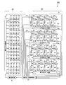
- FIG. 2A and FIG. 2B are outline views showing a schematic configuration of the solid-state imaging device 1 mounted on the imaging device 8 of the present embodiment.
- the solid-state imaging device 1 includes a first substrate 10, a second substrate 20, and an inter-substrate connection unit 30.
- FIG. 2A shows a side view of the solid-state imaging device 1
- FIG. 2B shows a plan view of each of the substrates constituting the solid-state imaging device 1.
- FIG. 2A In the solid-state imaging device 1, as shown in FIG. 2A, two substrates (chips) of a first substrate 10 and a second substrate 20 are stacked, and the first substrate 10 and the second substrate 20 are It is the structure joined (connected) by the board
- FIG. 2A In the solid-state imaging device 1, as shown in FIG. 2A, two substrates (chips) of a first substrate 10 and a second substrate 20 are stacked, and the first substrate 10 and the second substrate 20 are It is the structure joined (connected) by the board
- a pixel array unit 11 in which a plurality of pixels (hereinafter referred to as “unit pixels”) outputting pixel signals according to incident subject light (visible light) are arranged in a two-dimensional matrix on the first substrate 10 Is formed.
- the first substrate 10 is provided with a vertical readout circuit that reads pixel signals for each column from each unit pixel formed in the pixel array unit 11 and outputs the pixel signal to the second substrate 20.
- the second substrate 20 is provided with a plurality of column circuits for processing pixel signals output from respective unit pixels formed in the pixel array portion 11 of the first substrate 10 for each column of unit pixels,
- a signal processing circuit unit 21 is formed which externally outputs the pixel signal processed by the column circuit as an image signal for each row of unit pixels.
- the inter-substrate connection portion 30 is a connection portion for electrically connecting the components in the first substrate 10 and the components in the second substrate 20.
- the components disposed on the joined first substrate 10 and second substrate 20 transmit and receive respective electric signals via the corresponding inter-substrate connection portions 30.
- the first substrate 10 is a back-side illumination (BSI) silicon substrate in which subject light (visible light) is incident on the unit pixel formed in the pixel array unit 11 from the opposite side of the wiring layer.
- the first substrate 10 includes the pixel array unit 11 and the vertical readout circuit 12 as shown in (b-1) of FIG. 2B.
- the pixel array unit 11 is a pixel unit in which a plurality of unit pixels are arranged in a two-dimensional matrix.
- Each unit pixel in the pixel array unit 11 generates a signal charge according to incident light (visible light) and generates a photoelectric conversion unit, and amplifies the signal charge accumulated by the photoelectric conversion unit to generate a pixel signal.
- an amplification unit that outputs the Each unit pixel is provided with a pixel signal according to the subject light amplified by the amplification unit in the signal processing circuit unit 21 of the second substrate 20 according to the control signal input from the vertical readout circuit 12 To the column circuit to be output via the inter-substrate connection unit 30. A detailed description of this unit pixel will be described later.
- the vertical readout circuit 12 drives each unit pixel in the pixel array unit 11, and pixel signals corresponding to subject light generated and accumulated in each unit pixel are stored in the signal processing circuit unit 21 of the second substrate 20. Read out (output) the corresponding column circuit provided in.
- the vertical readout circuit 12 outputs a control signal for driving a unit pixel for each row of unit pixels arranged in the pixel array unit 11.
- the second substrate 20 includes a signal processing circuit unit 21 as shown in (b-2) of FIG. 2B.
- the signal processing circuit unit 21 corresponds to each column of unit pixels arranged in the pixel array unit 11 and is predetermined for each pixel signal sequentially input from the corresponding unit pixels.
- a plurality of column circuits are provided which output processed pixel signals after processing.
- the signal processing circuit unit 21 has a row of unit pixels disposed in the pixel array unit 11, which is an image signal processed by a column circuit corresponding to each of the unit pixels of each column disposed in the pixel array unit 11.
- a horizontal readout circuit is provided which sequentially reads out each time and outputs it to the outside.
- each unit pixel disposed in the pixel array unit 11 is divided into a plurality of regions (groups) in a form in which a plurality of rows are combined. For this reason, in the solid-state imaging device 1, vertical signal lines for outputting pixel signals from each unit pixel to the corresponding column circuit provided in the signal processing circuit unit 21 are divided into a plurality. For this reason, in the solid-state imaging device 1, the vertical readout circuit 12 can simultaneously output pixel signals to the corresponding column circuits in the unit pixels belonging to each group. That is, the vertical readout circuit 12 simultaneously drives unit pixels in a plurality of groups, as well as control signals for sequentially driving the respective unit pixels row by row and outputting pixel signals sequentially from each group.
- the signal processing circuit unit 21 is configured to correspond to each group of unit pixels. More specifically, a signal processing circuit (hereinafter referred to as “group signal processing circuit”) in which a plurality of column circuits corresponding to each column of unit pixels and one horizontal readout circuit are combined is referred to as “group signal processing circuit”. There are only a few. Further, in the solid-state imaging device 1, the inter-substrate connection unit 30 for transmitting the pixel signal output from each unit pixel to the corresponding group signal processing circuit is disposed for each of the divided vertical signal lines.
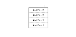
- FIGS. 2A and 2B show a configuration in which each unit pixel arranged in the pixel array unit 11 is divided into four groups, that is, the vertical signal line in the pixel array unit 11 is divided into four. .
- (b-2) of FIG. 2B four group signal processing circuits 221 corresponding to each group of unit pixels arranged in the pixel array unit 11 in the signal processing circuit unit 21.
- the case where the signal processing circuit 224 is provided is shown.
- FIG. 2A a substrate for connecting to a column circuit provided in each of the corresponding group signal processing circuit 221 to group signal processing circuit 224 for each group of unit pixels obtained by dividing the vertical signal line.
- the inter-substrate connection portion 30 is disposed, that is, the inter-substrate connection portion 30 is disposed for each of the divided vertical signal lines.
- the inter-substrate connection portion 30 for example, a micro bump manufactured by a vapor deposition method or a plating method, for example, a structure connected by a silicon through electrode (TSV: Through-Silicon-Via) or a metal wiring layer is used.
- TSV silicon through electrode
- a metal wiring layer for example, a metal wiring layer.
- inter-substrate connection of a plurality of structures according to positions where components in the first substrate 10 and components in the second substrate 20 are connected that is, positions where the inter-substrate connection portion 30 is formed.
- the unit 30 may be used.
- the components in the pixel array unit 11 formed on the first substrate 10 and the components in the signal processing circuit unit 21 formed on the second substrate 20 are electrically
- a micro through hole is used as the inter-substrate connection portion 30 to be connected in a random manner
- a silicon through electrode is used as the inter-substrate connection portion 30 to electrically connect the components other than the pixel array portion 11 It is also possible to use a configuration.
- each unit pixel arranged in the pixel array unit 11 is divided into a plurality of groups, and the vertical signal line in the pixel array unit 11 is divided into a plurality.
- the length of each vertical signal line can be shortened, and the number of unit pixels connected to each vertical signal line can be reduced.
- the load of each vertical signal line can be reduced.
- the respective unit pixels correspond. It is possible to realize speeding-up and low power consumption of readout of pixel signals to column circuits.
- the first substrate 10 in which the pixel array unit 11 is formed and the second substrate 20 in which the signal processing circuit unit 21 is formed are stacked.
- the vertical signal lines can be divided into a suitable number without restriction on the number of divisions of the vertical signal lines as in the configuration for reducing the load of the vertical signal lines in the device.
- the load on each vertical signal line is reduced without increasing the chip area, and speeding up and low power consumption of readout of pixel signals from each unit pixel to the corresponding column circuit Can be realized.
- the vertical readout circuit 12 simultaneously outputs control signals for reading out pixel signals from the respective unit pixels and outputting the pixel signals to the corresponding column circuits to each of the unit pixels belonging to different groups, that is, The unit pixels of different rows arranged in the pixel array unit 11 simultaneously output pixel signals to the corresponding column circuits.
- the solid-state imaging device 1 by reducing the load on each vertical signal line, the speed and power consumption of reading pixel signals from each unit pixel to the corresponding column circuit can be reduced. It is possible to achieve both the speeding up of the solid-state imaging device 1 by outputting in parallel the image signals processed by the column circuit.
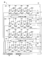
- FIG. 3 is a block diagram showing a schematic configuration of the solid-state imaging device 1 according to the first embodiment.
- the solid-state imaging device 1 of the first embodiment shown in FIG. 3 includes a first substrate 10 provided with a pixel array unit 11, a vertical readout circuit 12, and a pixel control unit 13, a signal processing circuit unit 21, and readout. And a second substrate 20 provided with the circuit control unit 23.
- unit pixels 110 are arranged in a two-dimensional matrix of 16 rows and 4 columns, and the arranged unit pixels 110 are divided into four groups. Then, the pixel array unit 11 divides each of the vertical signal lines corresponding to the arranged unit pixels 110 for each column into four. More specifically, the pixel array unit 11 divides all the arranged unit pixels 110 into a first group to a fourth group every 4 rows and 4 columns, and corresponds to the unit pixels 110 in the same column. The vertical signal line is divided into four.
- the signal processing circuit unit 21 includes four group signal processing circuits 221 to group signal processing circuits 224 corresponding to the first to fourth groups of the unit pixels 110 divided by the pixel array unit 11. Is equipped.
- Each of the group signal processing circuit 221 to the group signal processing circuit 224 includes pixel load current sources and column circuits whose number corresponds to the number of columns of the unit pixels 110 arranged in the pixel array unit 11, and the respective column circuits. And a horizontal readout circuit and an output unit. That is, each of the group signal processing circuit 221 to the group signal processing circuit 224 includes four pixel load current sources and four pixel load current sources corresponding to the respective columns of the unit pixels 110 arranged in four columns in the pixel array unit 11. It comprises a column circuit and one horizontal readout circuit and an output.
- the group signal processing circuit 221 corresponding to the first group in the pixel array unit 11 includes four pixel load current sources (pixels) respectively corresponding to the four columns of unit pixels 110 belonging to the first group.
- a load current source 2411 to a pixel load current source 2414), four column circuits (column circuits 2511 to 2514), a horizontal readout circuit 261, and an output unit 271 are provided.
- the group signal processing circuit 222 corresponding to the second group in the pixel array unit 11 includes four pixel load current sources (pixel load current sources 2421 respectively corresponding to the four columns of unit pixels 110 belonging to the second group.
- the pixel load current source 2424 four column circuits (column circuits 2521 to 2524), a horizontal readout circuit 262, and an output section 272 are provided.
- the group signal processing circuit 223 corresponding to the third group in the pixel array unit 11 includes four pixel load current sources (pixel load current sources 2431 respectively corresponding to the four columns of unit pixels 110 belonging to the third group.
- the pixel load current source 2434 four column circuits (column circuits 2531 to 2534), a horizontal readout circuit 263, and an output unit 273 are provided.
- the group signal processing circuit 224 corresponding to the fourth group in the pixel array unit 11 includes four pixel load current sources (pixel load current sources 2441 respectively corresponding to the four columns of unit pixels 110 belonging to the fourth group).
- the pixel load current source 2444), four column circuits (column circuit 2541 to column circuit 2544), a horizontal readout circuit 264, and an output unit 274 are provided.
- group signal processing circuit 22 when the group signal processing circuit 221, the group signal processing circuit 222, the group signal processing circuit 223, and the group signal processing circuit 224 are not distinguished from each other, “group signal processing circuit 22 "
- pixel load current source 241 When the pixel load current source 2411 to the pixel load current source 2414 in the group signal processing circuit 221 are not distinguished from one another, they are referred to as “pixel load current source 241”.
- pixel load current source 242 When the pixel load current source 2421 to the pixel load current source 2424 in the group signal processing circuit 222 are not distinguished from one another, they are referred to as “pixel load current source 242”.
- pixel load current source 2431 to the pixel load current source 2434 in the group signal processing circuit 223 are not distinguished, they are referred to as “pixel load current source 243”.
- pixel load current source 244 when the pixel load current source 2441 to the pixel load current source 2444 in the group signal processing circuit 224 are not distinguished from one another, they are referred to as “pixel load current source 244”.
- pixel load current source 2431 to the pixel load current source 2434 and the pixel load current source 2441 to the pixel load current source 2444 in the group signal processing circuit 224 are not distinguished from each other, they are referred to as “pixel load current source 24”.
- column circuits 2511 to 2514 in the group signal processing circuit 221 are not distinguished from one another, they are referred to as “column circuits 251”. Further, when the column circuits 2521 to 2524 in the group signal processing circuit 222 are not distinguished from one another, they are referred to as “column circuits 252”. Further, when the column circuits 2531 to 2534 in the group signal processing circuit 223 are not distinguished from one another, they are referred to as “column circuit 253”. Further, when the column circuits 2541 to 2544 in the group signal processing circuit 224 are not distinguished from one another, they are referred to as “column circuits 254”.
- column circuits 2541 to 2544 in the group signal processing circuit 224 are not distinguished from one another, they are referred to as "column circuits 25".
- the horizontal readout circuit 264 in the signal processing circuit 224 is not distinguished, it is referred to as “horizontal readout circuit 26”.
- an output unit 271 in the group signal processing circuit 221, an output unit 272 in the group signal processing circuit 222, an output unit 273 in the group signal processing circuit 223, and an output unit 274 in the group signal processing circuit 224 When it does not distinguish, it calls it "the output part 27.”
- Each unit pixel 110 in the pixel array unit 11 outputs a pixel signal corresponding to the incident subject light to the corresponding vertical signal line in accordance with the control signal input from the vertical readout circuit 12.
- Each of the vertical signal lines corresponding to the same row of unit pixels 110 in each group is supplied with the pixel load current in the corresponding group signal processing circuit 22 via the corresponding inter-substrate connection unit 30. Connected to the source and column circuit.
- the vertical signal line to which the four unit pixels 110 in the first column of the first group are connected is connected to the pixel load current corresponding to the group signal processing circuit 221 via the inter-substrate connection portion 311.
- Source 2411 and column circuit 2511 are connected.
- the vertical signal lines connected to the four unit pixels 110 in the second to fourth columns of the first group are group signals via the inter-substrate connection portion 312 to the inter-substrate connection portion 314, respectively.
- the processing circuit 221 is connected to corresponding pixel load current sources 2412 to 2414 and column circuits 2512 to 2514.
- the vertical signal lines connected to the four unit pixels 110 in the first to fourth columns of the second group are group signals via the inter-substrate connection portion 321 to the inter-substrate connection portion 324, respectively.
- the processing circuit 222 is connected to the corresponding pixel load current source 2421 to pixel load current source 2424 and to the column circuit 2521 to column circuit 2524.
- the vertical signal lines connected to the four unit pixels 110 in the first to fourth columns of the third group are group signals via the inter-substrate connection portion 331 to the inter-substrate connection portion 334, respectively.
- the processing circuit 223 is connected to the corresponding pixel load current source 2431 to the pixel load current source 2434 and the column circuit 2531 to the column circuit 2534.
- the vertical signal lines connected to the four unit pixels 110 in the first to fourth columns of the fourth group are group signals via the inter-substrate connection parts 341 to the inter-substrate connection parts 344, respectively.
- the processing circuit 224 is connected to the corresponding pixel load current source 2441 to the pixel load current source 2444 and the column circuit 2541 to the column circuit 2544.
- the pixel load current sources 24 in each of the group signal processing circuits 22 are current sources, one of which is connected to the ground of the group signal processing circuit 22 and the other of which is connected to the corresponding vertical signal line.
- the pixel load current source 24 operates as a load of the transistor of the amplification unit provided in the unit pixel 110 connected to the corresponding vertical signal line.
- the column circuits 25 in each of the group signal processing circuits 22 receive respective pixel signals sequentially input from the unit pixels 110 connected to the corresponding vertical signal line under the control of the readout circuit control unit 23. Is a processing circuit that performs predetermined processing. Each of the column circuits outputs an output signal after processing the input pixel signal to the corresponding output unit 27 according to the control from the horizontal readout circuit 26 in the group signal processing circuit 22. Do.
- the column circuit 25 may be, for example, a CDS (Correlated Double Sampling) circuit that performs noise suppression on a pixel signal, an amplification circuit that amplifies a pixel signal, or a pixel signal (analog signal).
- An analog-to-digital converter or the like which analog-digital converts and outputs a digital signal according to the size of the pixel signal can be considered.
- FIG. 3 shows the case where each column circuit 25 provided in the solid-state imaging device 1 of the first embodiment is an analog-to-digital converter (ADC).
- ADC analog-to-digital converter
- the analog-to-digital converter may have, for example, a function of performing CDS processing.
- the horizontal readout circuit 26 in each of the group signal processing circuits 22 sequentially reads out the processed output signals output from the corresponding column circuit 25 and causes the output unit 27 to sequentially output the processed output signals.
- the output unit 27 in each of the group signal processing circuits 22 outputs the processed output signal sequentially input from the corresponding column circuit 25 by the horizontal readout circuit 26 to the outside of the solid-state imaging device 1 as an image signal.
- the readout circuit control unit 23 controls the pixel control unit 13 provided on the first substrate 10 and the signal processing circuit unit 21 according to the operation mode when the solid-state imaging device 1 reads out the pixel signal and outputs it as an image signal.
- the column circuit 25 and the horizontal readout circuit 26 provided in each of the group signal processing circuits 22 are controlled. A detailed description of an operation mode in which the solid-state imaging device 1 outputs an image signal will be described later.
- the unit pixels 110 in the unit 11 are driven to control the method of reading out pixel signals.
- the vertical readout circuit 12 drives each unit pixel 110 in the pixel array unit 11 under the control of the pixel control unit 13 and outputs the pixel signal of each unit pixel 110 to the corresponding vertical signal line.
- the vertical readout circuit 12 can drive not only the unit pixels 110 provided in the pixel array unit 11 sequentially but also simultaneously drive the unit pixels 110 in a plurality of groups.
- each unit pixel 110 disposed in the pixel array unit 11 is divided into four groups (first group to fourth group). That is, by dividing the vertical signal line in the pixel array unit 11 into four, the length of each vertical signal line is shortened, and the number of unit pixels 110 connected to each vertical signal line is set. It is 1/4. That is, in the solid-state imaging device 1 according to the first embodiment, the load of each divided vertical signal line is reduced to 1/4 of the load of one column of vertical signal lines in the conventional solid-state imaging device. .
- the transistors of the amplification unit provided in the unit pixel 110 are It is possible to realize speeding-up and low power consumption of reading of pixel signals from each unit pixel 110 to the corresponding column circuit 25 without increasing the size.
- the group signal processing circuit 22 that is, the pixel load current source 24, the column circuit 25, for each vertical signal line divided in the pixel array unit 11.
- a horizontal readout circuit 26 and an output unit 27 are provided.
- the unit pixels 110 belonging to each group simultaneously output pixel signals to the corresponding group signal processing circuit 221 to group signal processing circuit 224.
- An image signal can be output simultaneously from each of the group signal processing circuit 221 to the group signal processing circuit 224. That is, in the solid-state imaging device 1 of the first embodiment, image signals for four lines can be simultaneously output to the outside. As a result, in the solid-state imaging device 1 according to the first embodiment, the speeding up of the output of the image signal can be realized.
- speeding up and reduction in power consumption of pixel signals from the unit pixel 110 to the column circuit 25 can be achieved by reducing the load on each vertical signal line. And the speeding-up of the solid-state imaging device 1 by outputting the image signals processed by the respective column circuits 25 in parallel can be compatible.
- FIG. 4 is a circuit diagram showing a schematic configuration of a unit pixel 110 in the pixel array unit 11 of the solid-state imaging device 1 according to the first embodiment.
- One unit pixel 110 is shown in FIG.
- a unit pixel 110 includes a photoelectric conversion unit PD, a transfer transistor M1, a charge storage unit FD, a pixel reset transistor M2, an amplification transistor M3, and a selection transistor M4.
- the unit pixel 110 converts the incident subject light (visible light) into a pixel signal and outputs the pixel signal to the vertical signal line 40.
- the photoelectric conversion unit PD photoelectrically converts incident object light to generate a signal charge, and accumulates the generated signal charge as a photoelectric conversion signal.
- the transfer transistor M1 transfers the photoelectric conversion signal accumulated in the photoelectric conversion unit PD to the gate terminal of the amplification transistor M3 in accordance with the control signal ⁇ TX input from the vertical readout circuit 12.
- the photoelectric conversion signal stored in the photoelectric conversion unit PD and transferred by the transfer transistor M1 is stored in the charge storage unit FD.
- the charge storage portion FD is a capacitance attached to a node connected to the gate terminal of the amplification transistor M3, and is indicated by a symbol of a capacitor in the schematic configuration of the unit pixel 110 shown in FIG.
- the amplification transistor M3 outputs a signal voltage corresponding to the photoelectric conversion signal transferred to the gate terminal by the transfer transistor M1, that is, the photoelectric conversion signal stored in the charge storage portion FD. At this time, the amplification transistor M3 outputs the photoelectric charge accumulated in the charge accumulation portion FD in accordance with the current value of the pixel load current source 24 connected to the corresponding vertical signal line 40 via the corresponding inter-substrate connection portion 30. A signal voltage obtained by amplifying the converted signal is output.
- the selection transistor M4 outputs the signal voltage output from the amplification transistor M3 to the vertical signal line 40 as a pixel signal in accordance with the control signal ⁇ SEL input from the vertical readout circuit 12. Thereby, the pixel signal corresponding to the photoelectric conversion signal generated and accumulated by the photoelectric conversion unit PD is read out to the vertical signal line 40.
- the pixel reset transistor M2 resets the photoelectric conversion signal in the unit pixel 110 to the power supply voltage VDD in accordance with the control signal ⁇ RST input from the vertical readout circuit 12.
- a pixel signal corresponding to a photoelectric conversion signal obtained by photoelectrically converting object light incident on the photoelectric conversion unit PD in the unit pixel 110 is transmitted to the corresponding column circuit 25 via the corresponding inter-substrate connection unit 30. It is input.
- the operation of the unit pixel 110 shown in FIG. 4 is the same as the operation of a unit pixel arranged in a general solid-state imaging device. Therefore, the detailed description of the operation of the unit pixel 110 will be omitted.
- FIG. 5A shows regions of first to fourth groups obtained by dividing all unit pixels 110 arranged in the pixel array unit 11 provided in the solid-state imaging device 1 into four groups.
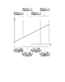
- 5B and 5C schematically show the transition of the row of unit pixels 110 outputting pixel signals in each operation mode of the solid-state imaging device 1, that is, the row transition of the pixel array unit 11 outputting as an image signal. It shows.
- the horizontal axis represents the time for the solid-state imaging device 1 to output an image signal according to the pixel signal output from each unit pixel 110, and the vertical axis represents the solid-state imaging device 1 for the pixel signal.
- a row of unit pixels 110 for outputting a corresponding image signal is shown.
- regions of all unit pixels 110 arranged in the pixel array unit 11 are divided into four groups of first to fourth groups.
- the vertical readout circuit 12 can not only drive the unit pixels 110 provided in the pixel array unit 11 sequentially but also drive the unit pixels 110 in a plurality of groups simultaneously.
- an operation mode hereinafter referred to as "parallel operation mode" in which unit pixels 110 in a plurality of groups are simultaneously driven to output image signals corresponding to pixel signals of a plurality of rows in parallel.
- FIG. 5B schematically shows transition of a row of unit pixels 110 in the parallel operation mode
- FIG. 5C schematically shows transition of a row of unit pixels 110 in the sequential operation mode.
- the camera control apparatus 5 with which the imaging device 8 was equipped performs switching of two operation modes, ie, the setting of a parallel operation mode or a sequential operation mode, for example. Then, in the imaging device 8, the operation mode of the solid-state imaging device 1 in which the image signal processing device 3 that processes the image signal output from the solid-state imaging device 1 is set (switched) by the camera control device 5 Perform processing according to
- the readout circuit control unit 23 outputs, to the pixel control unit 13, a control signal indicating that the image signal is output in the parallel operation mode. Thereby, the pixel control unit 13 instructs the vertical readout circuit 12 to simultaneously drive the unit pixels 110 belonging to the four groups and sequentially read out the pixel signals. In response to this instruction, the vertical readout circuit 12 drives the unit pixels 110 of the first row belonging to each of the first to fourth groups, and the respective pixel signals are transmitted to the first to fourth groups. Are output to the group signal processing circuit 22 corresponding to each.
- the readout circuit control unit 23 performs processing (here, analog-to-digital conversion processing) on pixel signals output from the unit pixels 110 belonging to the corresponding group to the respective column circuits 25 in the group signal processing circuit 22. Run it.
- the readout circuit control unit 23 causes the horizontal readout circuit 26 in the group signal processing circuit 22 to sequentially output the processed output signals output from the corresponding column circuits 25 to the output unit 27.
- the image signal corresponding to the pixel signal output from the unit pixel 110 of the first row belonging to each of the first to fourth groups is output in parallel by the output unit 27 in the group signal processing circuit 22. That is, image signals for four lines are simultaneously output to the outside.
- the vertical readout circuit 12 drives the unit pixels 110 of the next row belonging to each of the first group to the fourth group, and the respective pixel signals are set to each of the first group to the fourth group. It is output to the corresponding group signal processing circuit 22. Then, the readout circuit control unit 23 executes processing by each column circuit 25 in the group signal processing circuit 22 and sequentially outputs the output signal after processing by the horizontal readout circuit 26 to the output unit 27.
- the vertical readout circuit 12 sequentially drives the unit pixels 110 belonging to each of the first to fourth groups row by row to correspond to each of the first to fourth groups.
- the group signal processing circuit 22 sequentially outputs the respective pixel signals.
- the read out circuit control unit 23 sequentially performs the processing by each column circuit 25 in the group signal processing circuit 22 and the output to the output unit 27 of the processed output signal.
- the simultaneous output from the output unit 27 in the group signal processing circuit 22 of the image signal corresponding to the pixel signal output from the unit pixel 110 in the last row belonging to each of the first to fourth groups is When finished, the solid-state imaging device 1 completes the output of the image signal in the parallel operation mode.
- image signals corresponding to pixel signals output by unit pixels 110 belonging to each of the first to fourth groups are output in parallel. .
- the output of the image signal from the solid-state imaging device 1 can be speeded up.
- the readout circuit control unit 23 outputs, to the pixel control unit 13, a control signal indicating that the image signal is to be output sequentially in the operation mode.
- the pixel control unit 13 instructs the vertical readout circuit 12 to sequentially drive the unit pixels 110 belonging to the four groups, and to sequentially read out the pixel signals.
- the vertical readout circuit 12 drives the unit pixels 110 in the first row belonging to the first group, and causes each of the pixel signals to be output to the group signal processing circuit 221 corresponding to the first group. .
- the readout circuit control unit 23 processes the pixel signals output from the unit pixels 110 belonging to the first group corresponding to the respective column circuits 251 in the group signal processing circuit 221 (here, analog-to-digital conversion). Process) is executed. Further, the read out circuit control unit 23 causes the horizontal read out circuit 261 in the group signal processing circuit 221 to sequentially output the processed output signals output from the corresponding column circuits 251 to the output unit 271.
- an image signal corresponding to the pixel signal output from the unit pixels 110 in the first row belonging to the first group is output from the output unit 271 in the group signal processing circuit 221 to the outside.
- the vertical readout circuit 12 drives the unit pixels 110 in the next row belonging to the first group, and outputs the respective pixel signals to the group signal processing circuit 221 corresponding to the first group.
- the readout circuit control unit 23 executes processing by each column circuit 251 in the group signal processing circuit 221 and sequentially outputs the output signal after processing by the horizontal readout circuit 261 to the output unit 271.
- an image signal corresponding to the pixel signal output from the unit pixel 110 in the next row belonging to the first group is output from the output unit 271 in the group signal processing circuit 221.
- the vertical readout circuit 12 sequentially drives the unit pixels 110 belonging to the first group row by row, and sequentially outputs the respective pixel signals to the group signal processing circuit 221 corresponding to the first group.
- the read out circuit control unit 23 sequentially performs the processing by each column circuit 251 in the group signal processing circuit 221 and the output to the output unit 271 of the processed output signal.
- the vertical readout circuit 12 subsequently drives the unit pixels 110 of the first row belonging to the second group,
- the signal is output to the group signal processing circuit 222 corresponding to the second group.
- the readout circuit control unit 23 causes each column circuit 252 in the group signal processing circuit 222 to execute processing on the pixel signal output from the unit pixel 110 belonging to the corresponding second group, and the group signal
- the horizontal readout circuits 262 in the processing circuit 222 sequentially output the processed output signals output from the corresponding column circuits 252 to the output unit 272.
- the image signal corresponding to the pixel signal output from the unit pixel 110 of the first row belonging to the second group is a group following the pixel signal output from the unit pixel 110 of the last row of the first group.
- the signal is output from the output unit 272 in the signal processing circuit 222 to the outside.
- the vertical readout circuit 12 sequentially drives the unit pixels 110 belonging to the third group, and further, unit pixels 110 belonging to the third group. Subsequently, the unit pixels 110 belonging to the fourth group are sequentially driven to sequentially output the respective pixel signals to the corresponding group signal processing circuit 22. Further, the readout circuit control unit 23 executes processing by each column circuit 25 in the group signal processing circuit 22 corresponding to the unit pixel 110 driven by the vertical readout circuit 12, and an output signal after processing by the horizontal readout circuit 26. The sequential output to the output unit 27 is performed.
- the output from the output unit 272 in the group signal processing circuit 222 of the image signal according to the pixel signal output from the unit pixel 110 in the last row belonging to the second group it belongs to the third group.
- the image signal corresponding to the pixel signal output from the unit pixel 110 in the first row is sequentially output from the output unit 273 in the group signal processing circuit 223.
- the first belonging to the fourth group The image signal corresponding to the pixel signal output from the unit pixel 110 in the second row is sequentially output from the output unit 274 in the group signal processing circuit 224.
- the solid-state imaging device 1 When the output from the output unit 274 in the group signal processing circuit 224 of the image signal according to the pixel signal output from the unit pixel 110 in the last row belonging to the fourth group is completed, the solid-state imaging device 1 The output of the image signal in the sequential operation mode is completed.
- the image signal corresponding to the pixel signal output from the unit pixel 110 belonging to each of the first to fourth groups is The signal is sequentially output from the group signal processing circuit 221 to the group signal processing circuit 224 corresponding to the pixel 110.
- the sequential operation mode as in the conventional solid-state imaging device, it is possible to sequentially output the image signals according to the pixel signals output by all the unit pixels 110 arranged in the pixel array unit 11.
- each unit pixel 110 disposed in the pixel array unit 11 is divided into four groups, and the vertical signal lines are divided into four, so that the lengths of the respective vertical signal lines And the number of unit pixels 110 connected to each vertical signal line is 1/4.
- the load on each of the divided vertical signal lines is reduced to 1 ⁇ 4 of the load on one column of vertical signal lines in the conventional solid-state imaging device, and the image signal is output. Power consumption can be reduced compared to conventional solid-state imaging devices.
- the current values of the conventional solid-state imaging device and the pixel load current source are made equal, the readout from the pixel to the column circuit can be further speeded up.
- a plurality of groups in which a plurality of pixels (unit pixels 110) arranged in a two-dimensional matrix form are grouped in a predetermined plurality of rows.
- the first substrate (first substrate 10) having the pixel portion (pixel array portion 11) divided into four groups) and the same row in each of the first to fourth groups
- the pixel load current source (pixel load current source 24) corresponding to the vertical signal line (vertical signal line 40) to which the plurality of arranged unit pixels 110 are connected, and the output from the unit pixel 110 to the corresponding vertical signal line 40
- a column circuit for performing predetermined processing on the divided pixel signals for each column of unit pixels 110 belonging to each of the first to fourth groups, and the respective columns Pixel signal processed by the circuit 25
- a second substrate (a plurality of signal processing circuits (group signal processing circuits 22) for outputting each of the unit pixels 110 as an image signal corresponding to each of the first to fourth groups)
- the first substrate 10 and the second substrate 20 are
- each of the pixel load current source 24 and the column circuit 25 corresponding to each vertical signal line 40 A solid-state imaging device (solid-state imaging device 1) electrically connected via the respective inter-substrate connection portions (inter-substrate connection portions 30) corresponding to the lines 40 is configured.
- a plurality of groups in which a plurality of unit pixels 110 arranged in a two-dimensional matrix are grouped in a predetermined plurality of rows. And the plurality of unit pixels 110 arranged in the same column in each of the first to fourth groups are connected to each other.
- a second substrate 20 having a plurality of paths 22 corresponding to each of the first group to the fourth group, and the first substrate 10 and the second substrate 20 are stacked, Each vertical signal line 40 in each group of the group to fourth group and each vertical signal line 40 in the group signal processing circuit 22 corresponding to each group of the first group to fourth group
- the mechanical shutter for controlling the amount of light incident on the solid-state imaging device 1 is further provided, and each group of the first group to the fourth group
- the pixel signals output from the unit pixels 110 driven here are driven in parallel from the group signal processing circuits 22 corresponding to the respective groups of the first to fourth groups by simultaneously driving the unit pixels 110 in the
- the mechanical shutter 7 constitutes an imaging device 8 that blocks light incident on the solid-state imaging device 1.
- the first substrate 10 in which the pixel array unit 11 is formed and the second substrate 20 in which the signal processing circuit unit 21 is formed are the same. Make a stacked configuration.
- each unit pixel 110 disposed in the pixel array unit 11 can be divided into a plurality of groups without being limited in number.
- the vertical signal line to which the unit pixels 110 in the same column are connected in the pixel array unit 11 is divided into the number of groups into which the unit pixels 110 are divided. it can.
- the length of each vertical signal line can be shortened, and the number of unit pixels 110 connected to each vertical signal line can be reduced.
- the load of each divided vertical signal line can be reduced compared to the load of one vertical signal line in the conventional solid-state imaging device.
- the current value of the pixel load current source 24 corresponding to each unit pixel 110 is not increased, and the amplification transistor M3 provided in the unit pixel 110 is It is possible to realize speeding-up and low power consumption of reading of pixel signals from each unit pixel 110 to the corresponding column circuit 25 without increasing the size.
- the number of unit pixels 110 connected to each vertical signal line be equal. . That is, when dividing each unit pixel 110 arranged in the pixel array unit 11 into a plurality of groups in the solid-state imaging device 1 of the first embodiment, the number of unit pixels 110 belonging to each group is equal. Is desirable.
- the unit pixels 110 are divided into four groups, and the length of each vertical signal line in the pixel array unit 11 is made 1/4. In addition, the number of unit pixels 110 connected to each vertical signal line is reduced to 1/4, and the load on each vertical signal line is reduced to 1/4.
- the group signal processing circuit 22 corresponding to each group is provided in the second substrate 20. Then, in the solid-state imaging device 1 of the first embodiment, in the parallel operation mode, by simultaneously outputting pixel signals from the unit pixels 110 belonging to each group to the corresponding group signal processing circuit 22, Image signals for four lines are output from the signal processing circuit 22 simultaneously. As a result, in the solid-state imaging device 1 according to the first embodiment, the speeding up of the output of the image signal can be realized. At this time, in the solid-state imaging device 1 according to the first embodiment, since the load on each vertical signal line is reduced in each group, low power consumption can be realized when outputting an image signal. Can.
- the solid-state imaging device 1 of the first embodiment in the sequential operation mode, by sequentially outputting pixel signals to the corresponding group signal processing circuit 22 from the unit pixels 110 belonging to each group, Image signals are sequentially output from the signal processing circuits 22 to the outside.
- the solid-state imaging device 1 according to the first embodiment it is possible to realize low power consumption at the time of outputting an image signal by the effect of reducing the load of each vertical signal line in each group. it can.
- the solid-state imaging device 1 by reducing the load of each vertical signal line, it is possible to achieve both high speed and low power consumption.
- solid-state imaging device 100 The configuration of the solid-state imaging device 100 according to the second embodiment includes the same configuration as that of the solid-state imaging device 1 according to the first embodiment shown in FIG.
- the same components as the solid-state imaging device 1 of the first embodiment are the same as the solid-state imaging device 1 It demonstrates using the code
- FIG. 6 is a block diagram showing a schematic configuration of a solid-state imaging device 100 according to the second embodiment.
- two substrates (chips) of a first substrate 10 and a second substrate 20 are stacked, The first substrate 10 and the second substrate 20 are bonded (connected) at the inter-substrate connecting portion 30.
- the solid-state imaging device 100 according to the second embodiment shown in FIG. 6 includes the first substrate 10 including the pixel array unit 11, the vertical readout circuit 12, and the pixel control unit 13, the signal processing circuit unit 21, and the readout. And a second substrate 20 provided with a circuit control unit 23 and a power supply control unit 28.
- the solid-state imaging device 100 according to the second embodiment has a configuration in which a power control unit 28 is added to the configuration of the solid-state imaging device 1 according to the first embodiment shown in FIG.
- functions corresponding to the power control unit 28 are added to the corresponding components in the solid-state imaging device 100 according to the second embodiment.
- these components are the same as the respective components in the solid-state imaging device 1 according to the first embodiment, except for the functions added to correspond to the power control unit 28. That is, the operation of these components is the same as the operation of the corresponding components in the solid-state imaging device 1 of the first embodiment except for the operation according to the added function. Therefore, in the following description, in order to facilitate the description, the component to which the function corresponding to the power supply control unit 28 is added also uses the same reference numeral as the solid-state imaging device 1, and the operation according to the added function I will explain only about.
- the readout circuit control unit 23 controls the pixel control unit 13 provided on the first substrate 10 and the signal processing circuit unit 21 according to the operation mode when the solid-state imaging device 100 reads out the pixel signal and outputs it as an image signal.
- the column circuit 25 and the horizontal readout circuit 26 provided in each of the group signal processing circuits 22 are controlled. Further, the read out circuit control unit 23 controls the power supply control unit 28 in accordance with the operation mode of the solid-state imaging device 100.
- the power supply control unit 28 operates in the signal processing circuit unit 21 according to the control from the readout circuit control unit 23, that is, according to the operation mode when the solid-state imaging device 100 reads out the pixel signal and outputs it as an image signal.
- the power supplies of the components of the respective group signal processing circuits 22 are controlled. That is, the power of the component in the group signal processing circuit 22 which operates when the solid-state imaging device 100 outputs the current image signal is turned on, and the power of the component in the group signal processing circuit 22 which does not operate is selected. Turn off.
- the control of power ON or OFF in the power controller 28 is performed, for example, by controlling the supply of current to each component.
- the power supply control unit 28 includes the pixel load current source 24 provided in the group signal processing circuit 22 that operates when the solid-state imaging device 100 outputs the current image signal, the column circuit 25, and the horizontal readout circuit. 26 and the pixel load current source 24 provided in the group signal processing circuit 22 that supplies current to the output unit 27 and does not operate with the current image signal output, the column circuit 25, the horizontal readout circuit 26, and the output unit 27 Stop the supply of current.
- the group signal processing circuit 22 that outputs an image signal operates.
- a detailed description of the control of the power supply in each operation mode that is, the control of the power ON or OFF will be described later.
- each unit pixel 110 disposed in the pixel array unit 11 is not divided into the first as in the solid-state imaging device 1 according to the first embodiment.
- the length of each vertical signal line is shortened and the number of unit pixels 110 connected to each vertical signal line is reduced to 1 ⁇ 4.
- unit pixel 110 to column circuit 25 by reducing the load of each vertical signal line It is possible to achieve both the speeding-up of readout of pixel signals and the reduction of power consumption and the speeding-up of the solid-state imaging device 100 by outputting the image signals processed by the respective column circuits 25 in parallel.
- the solid-state imaging device 100 includes the power control unit 28. Then, the power control unit 28 controls the power of the components included in each of the group signal processing circuits 22 according to the operation mode in which the solid-state imaging device 100 reads the pixel signal and outputs it as an image signal. As a result, the current consumption by the components in the group signal processing circuit 22 that does not operate at the current output of the image signal is reduced, and the power consumption of the solid-state imaging device 100 can be further reduced.
- FIGS. 7A to 7C are diagrams showing a method of reading pixel signals in the solid-state imaging device 100 according to the second embodiment.
- FIG. 7A shows areas of first to fourth groups obtained by dividing all unit pixels 110 arranged in the pixel array unit 11 provided in the solid-state imaging device 100 into four groups.
- the region of all unit pixels 110 arranged in the pixel array unit 11 is a first group
- the fourth group is divided into four groups.
- the image signal can be output in two operation modes of the parallel operation mode and the sequential operation mode.
- the power control unit 28 controls the power of the group signal processing circuit 22 in accordance with the operation mode.
- FIG. 7B schematically shows the transition of the rows of unit pixels 110 in the parallel operation mode
- FIG. 7C schematically shows the transition of the rows of unit pixels 110 in the sequential operation mode.
- the horizontal axis indicates the time for the solid-state imaging device 100 to output an image signal according to the pixel signal output by each unit pixel 110
- the vertical axis indicates the solid-state imaging device 100 for the pixel signal
- a row of unit pixels 110 for outputting a corresponding image signal is shown.
- the readout circuit control unit 23 outputs a control signal indicating that an image signal is output in the parallel operation mode to the pixel control unit 13 and the power control unit 28.
- the power control unit 28 turns on the power of the components in all of the group signal processing circuits 22.
- the pixel control unit 13 instructs the vertical readout circuit 12 to simultaneously drive the unit pixels 110 belonging to the four groups to sequentially read out the pixel signals.
- the vertical readout circuit 12 sequentially drives from the unit pixels 110 of the first row belonging to each of the first group to the fourth group, and the respective pixel signals are first group to fourth group. It is sequentially output to the group signal processing circuit 22 corresponding to each of the groups.
- the readout circuit control unit 23 processes the pixel signals sequentially output from the unit pixels 110 belonging to the corresponding group to the column circuits 25 in the group signal processing circuit 22 (here, analog-to-digital conversion processing). To execute sequentially.
- the readout circuit control unit 23 causes the horizontal readout circuit 26 in the group signal processing circuit 22 to sequentially output the processed output signals sequentially output from the corresponding column circuits 25 to the output unit 27.
- the output unit 27 in the group signal processing circuit 22 parallels the image signals corresponding to the pixel signals sequentially output from the unit pixels 110 of the first row belonging to each of the first to fourth groups. That is, four lines of image signals are simultaneously and sequentially output to the outside.
- the power control unit 28 turns on the power of the components in all the group signal processing circuits 22. Therefore, the operation in the parallel operation mode in the solid-state imaging device 100 is the same as the operation in the parallel operation mode in the solid-state imaging device 1 according to the first embodiment. Therefore, the detailed description of the operation of the parallel operation mode in the solid-state imaging device 100 is omitted.
- the readout circuit control unit 23 outputs a control signal indicating that the image signal is output in the operation mode in sequence to the pixel control unit 13 and the power control unit 28.
- the pixel control unit 13 instructs the vertical readout circuit 12 to sequentially drive the unit pixels 110 belonging to the four groups, and to sequentially read out the pixel signals.
- the vertical readout circuit 12 sequentially drives from the unit pixels 110 of the first row belonging to the first group, and sequentially arranges respective pixel signals to the group signal processing circuit 221 corresponding to the first group. Make it output.
- the readout circuit control unit 23 processes the pixel signals sequentially output from the unit pixels 110 belonging to the corresponding first group to the respective column circuits 251 in the group signal processing circuit 221 (here, analog digital The conversion process is sequentially executed.
- the readout circuit control unit 23 causes the horizontal readout circuit 261 in the group signal processing circuit 221 to sequentially output the processed output signals sequentially output from the corresponding column circuits 251 to the output unit 271.
- the power supply control unit 28 generates the component (pixel load current in the group signal processing circuit 221).
- the power supply of the source 241, the column circuit 251, the horizontal readout circuit 261, and the output unit 271 is turned on.
- the power control unit 28 includes components in the group signal processing circuit 222 to the group signal processing circuit 224 (pixel load current source 242 to pixel load current source 244, column circuit 252 to column circuit 254, horizontal readout circuit 262 Power supply of the horizontal readout circuit 264 and the output unit 272 to the output unit 274 is turned off.
- the image signal corresponding to the pixel signal sequentially output from the unit pixels 110 in the first row belonging to the first group is sequentially output from the output unit 271 in the group signal processing circuit 221 to the outside.
- the vertical readout circuit 12 sequentially drives from the unit pixels 110 in the first row belonging to the second group.
- the pixel signals are sequentially output to the group signal processing circuit 222 corresponding to the second group.
- the readout circuit control unit 23 also causes each column circuit 252 in the group signal processing circuit 222 to sequentially execute processing on pixel signals sequentially output from the unit pixels 110 belonging to the corresponding second group,
- the horizontal readout circuit 262 in the signal processing circuit 222 sequentially outputs the processed output signals sequentially output from the corresponding column circuits 252 to the output unit 272.
- the power control unit 28 turns on the power of the components (the pixel load current source 242, the column circuit 252, the horizontal readout circuit 262, and the output unit 272) in the group signal processing circuit 222.
- the power supply control unit 28 includes the group signal processing circuit 221 and the components in the group signal processing circuit 223 to the group signal processing circuit 224 (pixel load current source 241 and pixel load current source 243 to pixel load current source Turn off the power supply of the column circuit 251 and the column circuit 253 to the column circuit 254, the horizontal readout circuit 261 and the horizontal readout circuit 263 to the horizontal readout circuit 264, and the output unit 271 and the output unit 273 Do.
- the image signal corresponding to the pixel signal sequentially output from the unit pixels 110 of the first row belonging to the second group follows the pixel signal output by the unit pixels 110 of the last row of the first group.
- the output unit 272 in the group signal processing circuit 222 sequentially outputs the signal to the outside.
- the vertical readout circuit 12 sequentially drives from the unit pixels 110 in the first row belonging to the third group.
- the pixel signals are sequentially output to the group signal processing circuit 223 corresponding to the third group.
- the readout circuit control unit 23 causes each column circuit 253 in the group signal processing circuit 223 to sequentially execute processing on pixel signals sequentially output from the unit pixels 110 belonging to the corresponding third group.
- the horizontal readout circuit 263 in the signal processing circuit 223 sequentially outputs the processed output signals sequentially output from the corresponding column circuits 253 to the output unit 273.
- the power control unit 28 turns on the power of the components (the pixel load current source 243, the column circuit 253, the horizontal readout circuit 263, and the output unit 273) in the group signal processing circuit 223.
- the power control unit 28 includes the group signal processing circuit 221 to the group signal processing circuit 222 and the components in the group signal processing circuit 224 (pixel load current source 241 to pixel load current source 242 and pixel load current source Turn OFF the power supply of the column circuits 251 to 252 and the column circuits 254, the horizontal readout circuit 261 to the horizontal readout circuit 262 and the horizontal readout circuit 264, and the output units 271 to 272 and the output unit 274).
- the image signal corresponding to the pixel signal sequentially output from the unit pixels 110 in the first row belonging to the third group follows the pixel signal output from the unit pixels 110 in the last row of the second group.
- the output unit 273 in the group signal processing circuit 223 sequentially outputs the signal to the outside.
- the vertical readout circuit 12 sequentially drives from the unit pixels 110 in the first row belonging to the fourth group.
- the pixel signals are sequentially output to the group signal processing circuit 224 corresponding to the fourth group.
- the readout circuit control unit 23 causes each column circuit 254 in the group signal processing circuit 224 to sequentially execute processing on pixel signals sequentially output from the unit pixels 110 belonging to the corresponding fourth group,
- the horizontal readout circuit 264 in the signal processing circuit 224 sequentially outputs the processed output signals sequentially output from the corresponding column circuits 254 to the output unit 274.
- the power supply control unit 28 turns on the power of the components (the pixel load current source 244, the column circuit 254, the horizontal readout circuit 264, and the output unit 274) in the group signal processing circuit 224.
- the power supply control unit 28 includes components in the group signal processing circuit 221 to the group signal processing circuit 223 (pixel load current source 241 to pixel load current source 243, column circuit 251 to column circuit 253, horizontal readout circuit 261 Power supply of the horizontal readout circuit 263 and the output units 271 to 273 is turned off.
- the image signal corresponding to the pixel signal sequentially output from the unit pixel 110 of the first row belonging to the fourth group follows the pixel signal output by the unit pixel 110 of the last row of the third group.
- the output unit 274 in the group signal processing circuit 224 sequentially outputs the signal to the outside.
- the solid-state imaging device 100 When the output from the output unit 274 in the group signal processing circuit 224 of the image signal according to the pixel signal output from the unit pixel 110 in the last row belonging to the fourth group is completed, the solid-state imaging device 100 The output of the image signal in the sequential operation mode is completed.
- the image signal corresponding to the pixel signal output from the unit pixel 110 belonging to each of the first to fourth groups is The signal is sequentially output from the group signal processing circuit 221 to the group signal processing circuit 224 corresponding to the pixel 110.
- the image signal output by the sequential operation mode in the solid-state imaging device 100 is the same as the image signal output by the sequential operation mode in the solid-state imaging device 1 of the first embodiment.
- the power control unit 28 turns on only the power of the components in the group signal processing circuit 22 that operates when outputting an image signal, and does not operate in the group signal processing circuit 22 that does not operate. The power of the components of is turned off.
- the power consumption can be further reduced by turning off the power of the components in the group signal processing circuit 22 which does not operate.
- the second substrate 20 further corresponds to the operation in the group signal processing circuit 22 according to the operation at the time of outputting an image signal from the solid-state imaging device (solid-state imaging device 100).
- a solid-state imaging device (solid-state imaging device 100) including a power control unit (power control unit 28) that controls the power of the components is configured.
- the power supply control unit 28 simultaneously drives the unit pixels 110 in each of the first group to the fourth group to generate the first to fourth groups.
- an image signal corresponding to the pixel signal output from the unit pixel 110 driven here is output from the solid-state imaging device 100 in parallel from the group signal processing circuit 22 corresponding to each group of the group, The power of all the components in the signal processing circuit 22 is turned ON, and each of the unit pixels 110 is sequentially driven, and the group signal processing circuit 22 corresponding to the unit pixel 110 driven here is driven here.
- an image signal corresponding to a pixel signal output from unit pixel 110 is sequentially output from solid-state imaging device 100, operation is performed to output the current image signal.
- the solid-state imaging device 100 turns on the power of the component in the group signal processing circuit 22 and turns off the power of the component in the group signal processing circuit 22 which does not operate to output the current image signal.
- the power control unit 28 includes components in the group signal processing circuit 22 including the output unit (output unit 27) provided in each of the group signal processing circuits 22.
- the solid-state imaging device 100 configured to control the ON state and the OFF state of the power supply of
- the first substrate 10 in which the pixel array unit 11 is formed and the second substrate 20 in which the signal processing circuit unit 21 is formed are the same. Make a stacked configuration.
- the number of unit pixels 110 arranged in the pixel array unit 11 is limited, as in the solid-state imaging device 1 of the first embodiment.
- the vertical signal lines to which the unit pixels 110 in the same column are connected in the pixel array unit 11 can be divided into the number of groups into which the unit pixels 110 are divided.
- the group signal processing circuit 22 corresponding to each group is provided in the second substrate 20. Then, in the solid-state imaging device 100 according to the second embodiment, in the sequential operation mode, only the power supplies of the components in the group signal processing circuit 22 that operate when outputting the image signal are turned on, and the group does not operate. The power of the components in the signal processing circuit 22 is turned off. Thereby, in the solid-state imaging device 100 according to the second embodiment, the effect of reducing the power consumption when outputting the image signal by reducing the load of each vertical signal line in each group in the sequential operation mode In addition to the above, it is possible to obtain an effect of reducing power consumption when outputting an image signal by controlling the power supply of the group signal processing circuit 22.
- the operation in the parallel operation mode is the same as the operation in the parallel operation mode in the solid-state imaging device 1 according to the first embodiment. Similar to the solid-state imaging device 1, it is possible to obtain an effect of reducing power consumption when outputting an image signal by reducing the load of each vertical signal line in each group.
- the power control unit 28 controls the power of the column circuit 25 and the horizontal readout circuit 26 in each of the group signal processing circuits 22.
- the configuration to control is shown. However, the control of the power supply between the column circuit 25 and the horizontal readout circuit 26 may be performed by the readout circuit control unit 23. Further, instead of the power supply control unit 28, the read out circuit control unit 23 may be configured to control the power supply of all the components in each of the group signal processing circuits 22.
- solid-state imaging device 200 The configuration of the solid-state imaging device 200 according to the third embodiment includes the same configuration as that of the solid-state imaging device 1 according to the first embodiment shown in FIG.
- the same components as the solid-state imaging device 1 of the first embodiment are the same as the solid-state imaging device 1 It demonstrates using the code
- FIG. 8 is a block diagram showing a schematic configuration of a solid-state imaging device 200 according to the third embodiment.
- the solid-state imaging device 200 of the third embodiment two substrates (chips) of the first substrate 10 and the second substrate 20 are stacked, The first substrate 10 and the second substrate 20 are bonded (connected) at the inter-substrate connecting portion 30.
- the solid-state imaging device 200 of the third embodiment shown in FIG. 8 includes a first substrate 10 provided with a pixel array unit 11, a vertical readout circuit 12, and a pixel control unit 13, a signal processing circuit unit 21, and readout. And a second substrate 20 provided with the circuit control unit 23.
- the solid-state imaging device 200 includes the group signal processing circuits 22 in the signal processing circuit unit 21 provided in the solid-state imaging device 1 according to the first embodiment shown in FIG.
- the configuration is such that a correction pixel (hereinafter referred to as “correction pixel”) corresponding to the column circuit 25 is added.
- each of the group signal processing circuits 22 includes the respective group signal processing circuits 22 in the signal processing circuit unit 21 provided in the solid-state imaging device 1 according to the first embodiment except that the correction pixels are added. Is the same as That is, the operation of each group signal processing circuit 22 is the same as the operation of the group signal processing circuit 22 of the solid-state imaging device 1 of the first embodiment except that the operation corresponding to the added correction pixel is performed. It is. Therefore, in the following description, the group signal processing circuit 22 to which the correction pixels are added also corresponds to the added correction pixels using the same reference numerals as the solid-state imaging device 1 to facilitate the description. Only the operation will be described.
- the readout circuit control unit 23 has a function of driving the correction pixels.
- the readout circuit control unit 23 is the same as the readout circuit control unit 23 in the solid-state imaging device 1 according to the first embodiment except for the function of driving the correction pixels. Therefore, in the following description, in order to facilitate the description, the readout circuit control unit 23 to which the function of driving the correction pixel is added also uses the same reference numeral as the solid-state imaging device 1 and corresponds to the added function. Only the operation of the
- the signal processing circuit unit 21 includes four groups corresponding to the first to fourth groups of unit pixels 110 divided by the pixel array unit 11.
- Signal processing circuit 221 to group signal processing circuit 224 includes a number of correction pixels, a pixel load current source, and a column circuit according to the number of columns of the unit pixels 110 arranged in the pixel array unit 11.
- a horizontal readout circuit and an output unit common to the respective column circuits. That is, each of the group signal processing circuit 221 to the group signal processing circuit 224 includes four correction pixels corresponding to the respective columns of the unit pixels 110 arranged in four columns in the pixel array unit 11, and a pixel load current.
- a source and column circuit and one horizontal readout circuit and an output are provided.
- the group signal processing circuit 221 corresponding to the first group in the pixel array unit 11 includes four correction pixels (for correction) respectively corresponding to the four columns of unit pixels 110 belonging to the first group.
- the pixel 2911 to the correction pixel 2914), four pixel load current sources 241, four column circuits 251, a horizontal readout circuit 261, and an output unit 271 are provided.
- the group signal processing circuit 222 corresponding to the second group in the pixel array unit 11 includes four correction pixels (correction pixels 2921 to correction) respectively corresponding to the four columns of unit pixels 110 belonging to the second group.
- Pixel 2924 includes four correction pixels (correction pixels 2921 to correction) respectively corresponding to the four columns of unit pixels 110 belonging to the second group.
- the group signal processing circuit 223 corresponding to the third group in the pixel array unit 11 includes four correction pixels (correction pixels 2931 to correction corresponding to the four columns of unit pixels 110 belonging to the third group).
- Pixel 2934 includes four pixel load current sources 243, four column circuits 253, a horizontal readout circuit 263, and an output unit 273.
- the group signal processing circuit 224 corresponding to the fourth group in the pixel array unit 11 includes four correction pixels (correction pixels 2941 to correction corresponding to the four columns of unit pixels 110 belonging to the fourth group).
- Pixel 2944 four pixel load current sources 244, four column circuits 254, a horizontal readout circuit 264, and an output section 274.
- correction pixels 2911 to 2914 in the group signal processing circuit 221 are not distinguished from each other, they are referred to as “correction pixels 291”.
- correction pixels 2921 to 2924 in the group signal processing circuit 222 are not distinguished from one another, they are referred to as “correction pixels 292”.
- correction pixels 2931 to the correction pixels 2934 in the group signal processing circuit 223 are not distinguished from one another, they are referred to as “correction pixels 293”.
- correction pixels 2941 to 2944 in the group signal processing circuit 224 are not distinguished from one another, they are referred to as “correction pixels 294”.
- correction pixels 2911 to 2914 in the group signal processing circuit 221 correction pixels 2921 to correction pixels 2924 in the group signal processing circuit 222, and correction pixels 2931 in the group signal processing circuit 223.
- correction pixels 2934 and the correction pixels 2941 to 2944 in the group signal processing circuit 224 are not distinguished from one another, they are referred to as “correction pixels 29”.
- the correction pixels 29 in each of the group signal processing circuits 22 correct the column circuits 25 included in each of the group signal processing circuits 22 in accordance with the control signal input from the readout circuit control unit 23. It is a pixel having a configuration similar to that of the unit pixel 110, which outputs a correction pixel signal. However, while the unit pixel 110 outputs a pixel signal corresponding to the subject light, the correction pixel 29 corresponds to the vertical signal line corresponding to the correction pixel signal corresponding to the voltage value of the predetermined reference voltage. Output to As a result, correction pixel signals corresponding to predetermined voltage values are input to the corresponding column circuits 25.
- the pixel load current source 24 in each of the group signal processing circuits 22 also operates as a load of a transistor of an amplification unit provided in the correction pixel 29 connected to the corresponding vertical signal line.
- the detailed description of the correction pixel 29 will be described later.
- the readout circuit control unit 23 controls the pixel control unit 13 provided on the first substrate 10 and the signal processing circuit unit 21 according to the operation mode when the solid-state imaging device 200 reads out the pixel signal and outputs it as an image signal.
- the column circuit 25 and the horizontal readout circuit 26 provided in each of the group signal processing circuits 22 are controlled.
- the readout circuit control unit 23 drives the correction pixels 29 in each of the group signal processing circuits 22 in the same manner as the vertical readout circuit 12 and corresponds to the correction pixel signals output from the respective correction pixels 29. It makes the column circuit 25 read out (output).
- the readout circuit control unit 23 can also output a control signal for driving the correction pixels 29 to each of the group signal processing circuits 22, but can also output them simultaneously to all the correction pixels 29. .
- the readout circuit control unit 23 drives the correction pixels 29 in each of the group signal processing circuits 22 before the solid-state imaging device 200 outputs an image signal corresponding to the pixel signal in each operation mode.
- the column circuit 25 in the group signal processing circuit 22 processes the correction pixel signal. Then, the read out circuit control unit 23 corrects the respective column circuits 25 so that the respective output signals after processing the correction pixel signals become the same.
- the output signal of each column circuit 25 is read, and based on the output signal read from all the column circuits 25, each column circuit 25 is identical.
- a correction value for correcting to output an output signal of The readout circuit control unit 23 outputs an image signal corresponding to the pixel signal according to each operation mode, that is, causes each column circuit 25 to process the pixel signal output from the unit pixel 110.
- the respective column circuits 25 are controlled in accordance with the calculated correction value. Thereby, the solid-state imaging device 200 can output an image signal in which the reference level of the pixel signal output from each unit pixel 110 is corrected.
- the signal processing circuit for each group is output before the image signal corresponding to the pixel signal output by the unit pixel 110 is output in each operation mode. 22 correct the level of the output signal output from the column circuit 25.
- the vertical signal line to which the unit pixels 110 in the same column are connected in the pixel array unit 11 is divided into groups into which the unit pixels 110 are divided. It is possible to reduce the level difference of the output signals output from the column circuit 25 in the group signal processing circuit 22 corresponding to each group. As a result, in each of the areas (groups) obtained by dividing the unit pixel 110 in the image (still image or moving image) generated by the imaging device 8 equipped with the solid-state imaging device 200 of the third embodiment Level difference) can be suppressed.
- the correction pixel 29 has a voltage value of a predetermined reference voltage instead of a pixel signal corresponding to a photoelectric conversion signal obtained by photoelectric conversion of subject light incident on the photoelectric conversion unit PD in the unit pixel 110 shown in FIG. It outputs a correction pixel signal according to that. Therefore, the correction pixel 29 includes the same configuration as that of the unit pixel 110. Therefore, in the following description, components similar to the unit pixel 110 in the respective components of the correction pixel 29 will be described using the same reference numerals as the unit pixel 110.
- FIG. 9 is a circuit diagram showing a schematic configuration of the correction pixel 29 in the signal processing circuit unit 21 of the solid-state imaging device 200 of the third embodiment.
- One correction pixel 29 is shown in FIG.
- the correction pixel 29 includes a transfer transistor M1, a charge storage unit FD, a pixel reset transistor M2, an amplification transistor M3, and a selection transistor M4.
- the transfer transistor M1 transfers the voltage value of the reference voltage Vtest to the gate terminal of the amplification transistor M3 in accordance with the control signal ⁇ TX input from the read out circuit control unit 23.
- the voltage value of the reference voltage Vtest transferred by the transfer transistor M1 is stored in the charge storage unit FD.
- the charge storage portion FD is a capacitance associated with a node connected to the gate terminal of the amplification transistor M3, and is indicated by a symbol of a capacitor in the schematic configuration of the correction pixel 29 shown in FIG.
- the amplification transistor M3 outputs a signal voltage according to the voltage value of the reference voltage Vtest transferred to the gate terminal by the transfer transistor M1, that is, the voltage value of the reference voltage Vtest stored in the charge storage portion FD. At this time, the amplification transistor M3 amplifies the voltage value of the reference voltage Vtest stored in the charge storage portion FD in accordance with the current value of the pixel load current source 24 connected to the corresponding vertical signal line 40. Output.
- the selection transistor M4 outputs the signal voltage output from the amplification transistor M3 to the vertical signal line 40 as a correction pixel signal in accordance with the control signal ⁇ SEL input from the readout circuit control unit 23. Thereby, the correction pixel signal corresponding to the voltage value of the reference voltage Vtest is read out to the vertical signal line 40 in a state corresponding to the pixel signal output from the unit pixel 110.
- the pixel reset transistor M2 resets the voltage value of the reference voltage Vtest in the correction pixel 29 to the power supply voltage VDD according to the control signal ⁇ RST input from the read out circuit control unit 23.
- the correction pixel signal according to the voltage value of the reference voltage Vtest in the correction pixel 29 is input to the corresponding column circuit 25.
- the operation of the correction pixel 29 shown in FIG. 9 is the same as the operation of the unit pixel 110. Therefore, detailed description of the operation of the correction pixel 29 is omitted.
- the group signal processing circuits 22 further correspond to the respective column circuits 25 and correspond to the vertical signal lines 40 to which the corresponding column circuits 25 are connected.
- a solid-state imaging device (solid-state imaging device 200) including a correction pixel (correction pixel 29) for outputting a correction pixel signal for correcting the column circuit 25 is configured.
- each of the column circuits 25 provided in each of the group signal processing circuits 22 is used as a corresponding correction pixel 29.
- a solid-state imaging device 200 is configured to perform correction using the correction pixel signal output by
- the first substrate 10 in which the pixel array unit 11 is formed and the second substrate 20 in which the signal processing circuit unit 21 is formed are the same. Make a stacked configuration.
- the number of unit pixels 110 arranged in the pixel array unit 11 is limited, as in the solid-state imaging device 1 of the first embodiment.
- the vertical signal lines to which the unit pixels 110 in the same column are connected in the pixel array unit 11 can be divided into the number of groups into which the unit pixels 110 are divided.
- the group signal processing circuit 22 corresponding to each group is provided in the second substrate 20.
- the correction pixel 29 is provided in each of the group signal processing circuits 22.
- the output signal from each column circuit 25 is read a plurality of times according to the correction pixel signal output from the correction pixel 29 provided in each group signal processing circuit 22, and based on each output signal It is desirable to calculate the correction value.
- the influence of the random variation of the correction pixel signal output from the correction pixel 29 can be reduced.
- the accuracy of correction can be improved, such as suppressing the influence of noise on the output signal output from the same column circuit 25.
- the solid-state imaging device 200 according to the third embodiment as well as the solid-state imaging device 1 according to the first embodiment, speeding up and power consumption reduction can be achieved by reducing the load on each vertical signal line. And both. Further, in the solid-state imaging device 200 of the third embodiment, the level difference (step) between the column circuits 25 in the group signal processing circuit 22 corresponding to each of the divided vertical signal lines is suppressed to reduce the third difference.
- the imaging device 8 equipped with the solid-state imaging device 200 of the embodiment can generate a good image.
- the configuration in which one correction pixel 29 is provided for each column circuit 25 in each of the group signal processing circuits 22 has been described.
- the number of correction pixels 29 corresponding to each column circuit 25 is not limited to the configuration shown in FIG. 8, that is, one.
- a plurality of correction pixels 29 can be provided to one column circuit 25.
- the readout circuit control unit 23 can perform the correction of the respective column circuits 25 based on the respective correction pixel signals output by the corresponding plurality of correction pixels 29, and The influence of fixed variations can be reduced.
- the accuracy of correction can be improved, such as suppressing the influence of noise in the output signal output from the column circuit 25 in accordance with each correction pixel signal used for calculation of the correction value.
- the number of rows of unit pixels 110 arranged in the group to which the column circuit 25 corresponds corresponds to the group signal processing circuit.
- the maximum number of correction pixels 29 provided in the group 22 is considered to be the maximum number of correction pixels in the group signal processing circuit 22, such as every plural rows of unit pixels 110 arranged in the group. It can be determined within the range where 29 can be arranged.
- the correction of the column circuit 25 by the readout circuit control unit 23 is performed each time the solid-state imaging device 200 outputs an image signal according to the pixel signal in each operation mode, that is, the solid-state imaging device 200 outputs each frame. It can be done every time before outputting an image signal. However, for example, by providing a storage unit for holding the correction value in the read out circuit control unit 23, the column circuit 25 can be corrected at a predetermined timing. For example, when the imaging device 8 equipped with the solid-state imaging device 200 of the third embodiment starts up, when the operation mode of the solid-state imaging device 200 is changed, or at a predetermined periodic timing, etc. The correction value held in the read out circuit control unit 23 may be updated.
- the photoelectric conversion unit PD is deleted from the component of the unit pixel 110, and instead, the voltage value of the reference voltage Vtest determined in advance is transferred to the amplification transistor M3 by the transfer transistor M1.
- the structure similar to the unit pixel 110 which transfers to a gate terminal was demonstrated.
- the configuration of the correction pixel 29 is not limited to the configuration shown in FIG.
- the correction pixel 29 can also have the same configuration as that of the unit pixel 110, that is, a configuration including the photoelectric conversion unit PD.
- the pixel where the correction pixel signal output from the correction pixel 29 is output by the unit pixel 110 of the plurality of optical black (OB) regions always shielded. Like signals, it can be used to correct for black level variations on pixel signals. This is because the correction pixels 29 are formed in the second substrate 20, so it is easy to shield the correction pixels 29 from light.
- the area of the unit pixel 110 in the pixel array unit 11 is divided into groups, that is, the center of the pixel array unit 11. Even if it is a partial region, the same configuration as the configuration in which the optical black (OB) region is provided can be used.
- the correction pixel 29 is considered to be superior to the configuration shown in FIG. . Even with this configuration, the correction pixel signal output from the correction pixel 29 can be processed in the same manner as the pixel signal output from the unit pixel 110 in the optical black (OB) area.
- OB optical black
- the respective group signal processing circuits 22 are separately provided.
- solid-state imaging device 300 The configuration of the solid-state imaging device 300 according to the fourth embodiment includes the same configuration as that of the solid-state imaging device 100 according to the second embodiment shown in FIG.
- the same components as the solid-state imaging device 100 of the second embodiment are the same as the solid-state imaging device 100. It demonstrates using the code
- FIG. 10 is a block diagram showing a schematic configuration of the second substrate 20 of the solid-state imaging device 300 according to the fourth embodiment.
- the solid-state imaging device 300 of the fourth embodiment two substrates (chips) of the first substrate 10 and the second substrate 20 are stacked, The first substrate 10 and the second substrate 20 are bonded (connected) at the inter-substrate connecting portion 30.
- the configuration of the first substrate 10 in the solid-state imaging device 300 according to the fourth embodiment is the same as the solid-state imaging device 1 according to the first embodiment, the solid-state imaging device 100 according to the second embodiment, and the third embodiment.
- the configuration is the same as that of the first substrate 10 of the solid-state imaging device 200 according to the embodiment. Therefore, FIG. 10 shows only the configuration of the second substrate 20 of the solid-state imaging device 300 of the fourth embodiment.
- the second substrate 20 of the solid-state imaging device 300 according to the fourth embodiment shown in FIG. 10 includes a signal processing circuit unit 21, a readout circuit control unit 23, and a power control unit 28.
- the second substrate 20 of the solid-state imaging device 300 according to the fourth embodiment has the group signal processing provided in the signal processing circuit unit 21 in the configuration of the solid-state imaging device 100 according to the second embodiment shown in FIG.
- the circuit 22 is configured to share the horizontal readout circuit 26. More specifically, each of the group signal processing circuit 221 and the group signal processing circuit 222 share the horizontal readout circuit, and each of the group signal processing circuit 223 and the group signal processing circuit 224 is horizontal.
- the read circuit is shared.
- the horizontal readout circuit shared by each of the group signal processing circuit 221 and the group signal processing circuit 222 is referred to as “horizontal readout circuit 2612”, and the group signal processing circuit 222 and the group signal processing are performed.
- the horizontal readout circuit shared by each of the circuits 223 is referred to as “horizontal readout circuit 2634”.
- each of the group signal processing circuits 22 is the same as the group signal processing circuit 22 provided in the solid-state imaging device 100 of the second embodiment except that the horizontal readout circuit 26 is shared, that is, the group signal processing The operation of each of the circuits 22 is similar. Therefore, in the following description, in order to facilitate the description, the description of the same components as the group signal processing circuit 22 provided in the solid-state imaging device 100 according to the second embodiment will be omitted.
- the power supply control unit 28 operates in the signal processing circuit unit 21 according to the control from the readout circuit control unit 23, that is, according to the operation mode when the solid-state imaging device 300 reads out the pixel signal and outputs it as an image signal.
- the power supply of each group signal processing circuit 22 is controlled.
- the power supply control unit 28 includes the pixel load current source 24, the column circuit 25, and the output unit 27 included in the group signal processing circuit 22 that operates when the solid-state imaging device 300 outputs the current image signal. Only the power supply of the horizontal readout circuit 26 shared by the respective group signal processing circuits 22 is controlled to the ON state.
- the horizontal readout circuit 26 shared by each of the group signal processing circuits 22 sequentially reads out the processed output signal output from the corresponding column circuit 25 and causes the corresponding output unit 27 to sequentially output it.
- the output unit 27 in each of the group signal processing circuits 22 outputs the processed output signal sequentially input from the corresponding column circuit 25 by the corresponding horizontal readout circuit 26 to the outside of the solid-state imaging device 300 as an image signal. Do.
- the solid-state imaging device 1 of the first embodiment, the solid-state imaging device 100 of the second embodiment, and the solid state of the third embodiment A solid-state imaging device by speeding up and reducing the power consumption of reading pixel signals from the unit pixels 110 to the column circuits 25 and outputting image signals processed by the respective column circuits 25 in parallel, as in the imaging device 200 It is compatible with 300 speeding up.
- the horizontal readout circuit 26 is shared by the respective group signal processing circuits 22. Therefore, the solid-state imaging device 1 of the first embodiment, the second The circuit scale can be smaller than that of the solid-state imaging device 100 of the embodiment and the solid-state imaging device 200 of the third embodiment.
- 11A to 11C are diagrams showing a method of reading pixel signals in the solid-state imaging device 300 according to the fourth embodiment.
- the regions of all the unit pixels 110 arranged in the pixel array unit 11 are divided into first to fourth groups. It is divided into four groups. Therefore, even in the solid-state imaging device 300 of the fourth embodiment, the solid-state imaging device 1 of the first embodiment, the solid-state imaging device 100 of the second embodiment, and the solid-state imaging device 200 of the third embodiment Similarly, the image signal can be output in two operation modes of the parallel operation mode and the sequential operation mode.
- FIG. 11B schematically shows the transition of the row of unit pixels 110 in the parallel operation mode
- FIG. 11C schematically shows the transition of the row of unit pixels 110 in the sequential operation mode.
- the power control unit 28 controls the power of the group signal processing circuit 22 according to the operation mode.
- the horizontal axis represents the time for the solid-state imaging device 300 to output an image signal corresponding to the pixel signal output by each unit pixel 110
- the vertical axis represents the solid-state imaging device 300 for the pixel signal.
- a row of unit pixels 110 for outputting a corresponding image signal is shown.
- the power control unit 28 turns on the power of the components in all of the group signal processing circuits 22. Then, in the operation in the parallel operation mode in the solid-state imaging device 300, one horizontal readout circuit 26 shared by the two group signal processing circuits 22 is output from the column circuit 25 in the shared group signal processing circuit 22. At the same time, the output signals after the processing are read out sequentially and output to the corresponding output unit 27 sequentially.
- the operation of the parallel operation mode in the solid-state imaging device 300 is the solid-state imaging device 1 of the first embodiment, the solid-state imaging device 100 of the second embodiment, and the solid state of the third embodiment. The operation is similar to that of the parallel operation mode in the imaging device 200. Therefore, detailed description of the operation of the parallel operation mode in the solid-state imaging device 300 will be omitted.
- the group control signal operates when the power control unit 28 outputs the current image signal.
- the power supply of only the processing circuit 22 is controlled to the ON state.
- the power supply control unit 28 controls the pixel load current included in the group signal processing circuit 221. Only the power sources of the source 241, the column circuit 251, and the output unit 271, and the horizontal readout circuit 2612 shared by the group signal processing circuit 221 and the group signal processing circuit 222 are controlled to be in the ON state. Further, during a period in which the solid-state imaging device 300 outputs the image signal of the second group, as illustrated in FIG.
- the power supply control unit 28 includes the pixel load current source 242 provided in the group signal processing circuit 222; Only the power supplies of the circuit 252 and the output unit 272 and the horizontal readout circuit 2612 shared by the group signal processing circuit 221 and the group signal processing circuit 222 are controlled to be in the ON state. Further, during a period in which the solid-state imaging device 300 outputs the image signal of the third group, as illustrated in FIG. 11B, the power supply control unit 28 includes the pixel load current source 243 provided in the group signal processing circuit 223; Only the power supplies of the circuit 253 and the output unit 273 and the horizontal readout circuit 2634 shared by the group signal processing circuit 223 and the group signal processing circuit 224 are controlled to be in the ON state.
- the power supply control unit 28 includes the pixel load current source 244 provided in the group signal processing circuit 224; Only the power supplies of the circuit 254 and the output unit 274, and the horizontal readout circuit 2634 shared by the group signal processing circuit 223 and the group signal processing circuit 224 are controlled to the ON state.
- the readout circuit control unit 23 sequentially outputs a control signal indicating that the image signal is output in the operation mode. Output to 28 and.
- the pixel control unit 13 instructs the vertical readout circuit 12 to sequentially drive the unit pixels 110 belonging to the four groups, and to sequentially read out the pixel signals.
- the vertical readout circuit 12 sequentially drives from the unit pixels 110 of the first row belonging to the first group, and sequentially arranges respective pixel signals to the group signal processing circuit 221 corresponding to the first group. Make it output.
- the readout circuit control unit 23 processes the pixel signals sequentially output from the unit pixels 110 belonging to the corresponding first group to the respective column circuits 251 in the group signal processing circuit 221 (here, analog digital The conversion process is sequentially executed.
- the readout circuit control unit 23 sequentially loads the horizontal readout circuit 2612 shared by the group signal processing circuit 221 and the group signal processing circuit 222 from the corresponding column circuits 251 in the group signal processing circuit 221. The output signal after the processing is output to the output unit 271 sequentially.
- the power supply control unit 28 operates when outputting the image signal of the first group in accordance with the control signal representing the output of the image signal in the sequential operation mode input from the reading circuit control unit 23.
- the power of the component is turned on, and the power of the component that operates when outputting the image signals of the second to fourth groups is turned off.
- the power supply control unit 28 includes the pixel load current source 241, the column circuit 251, the output unit 271, the group signal processing circuit 221, and the group signal processing circuit 222 provided in the group signal processing circuit 221.
- the power control unit 28 turns off the power of the pixel load current source 242 provided in the group signal processing circuit 222, the column circuit 252, and the output unit 272.
- the power supply control unit 28 includes the pixel load current source 243 provided in the group signal processing circuit 223, the column circuit 253, and the output unit 273, and the pixel load current source 244 provided in the group signal processing circuit 224, the column circuit.
- the power supplies of the output section 274 and the horizontal readout circuit 2634 shared by the group signal processing circuit 223 and the group signal processing circuit 224 are turned off.
- the image signal corresponding to the pixel signal sequentially output from the unit pixels 110 in the first row belonging to the first group is sequentially output from the output unit 271 in the group signal processing circuit 221 to the outside.
- the vertical readout circuit 12 sequentially drives from the unit pixels 110 in the first row belonging to the second group.
- the pixel signals are sequentially output to the group signal processing circuit 222 corresponding to the second group.
- the readout circuit control unit 23 causes each column circuit 252 in the group signal processing circuit 222 to sequentially execute processing on pixel signals sequentially output from the unit pixels 110 belonging to the corresponding second group. In addition, the readout circuit control unit 23 sequentially loads the horizontal readout circuit 2612 shared by the group signal processing circuit 221 and the group signal processing circuit 222 from the corresponding column circuits 252 in the group signal processing circuit 222. The output signal after the processing is output to the output unit 272 sequentially.
- the power control unit 28 turns on the power of the component that operates when outputting the image signal of the second group, and the image signal of the second group and the third to fourth groups. Turn off the power of the component that operates when outputting. More specifically, the power supply control unit 28 includes the pixel load current source 242, the column circuit 252, and the output unit 272 provided in the group signal processing circuit 222, the group signal processing circuit 221, and the group signal processing circuit 222. And turns on only the power supply with the horizontal readout circuit 2612 shared by the Further, the power supply control unit 28 turns off the power supply of the pixel load current source 241, the column circuit 251, and the output unit 271 included in the group signal processing circuit 221.
- the power supply control unit 28 includes the pixel load current source 243 provided in the group signal processing circuit 223, the column circuit 253, and the output unit 273, and the pixel load current source 244 provided in the group signal processing circuit 224, the column circuit.
- the power supplies of the output section 274 and the horizontal readout circuit 2634 shared by the group signal processing circuit 223 and the group signal processing circuit 224 are turned off.
- the image signal corresponding to the pixel signal sequentially output from the unit pixels 110 of the first row belonging to the second group follows the pixel signal output by the unit pixels 110 of the last row of the first group.
- the output unit 272 in the group signal processing circuit 222 sequentially outputs the signal to the outside.
- the vertical readout circuit 12 sequentially drives from the unit pixels 110 in the first row belonging to the third group.
- the pixel signals are sequentially output to the group signal processing circuit 223 corresponding to the third group.
- the read out circuit control unit 23 causes the respective column circuits 253 in the group signal processing circuit 223 to sequentially execute processing on pixel signals sequentially output from the unit pixels 110 belonging to the corresponding third group.
- the readout circuit control unit 23 sequentially loads the horizontal readout circuit 2634 shared by the group signal processing circuit 223 and the group signal processing circuit 224 from the corresponding column circuits 253 in the group signal processing circuit 223.
- the output unit 273 sequentially outputs the output signals after the output processing.
- the power control unit 28 turns on the power of the component that operates when outputting the image signal of the third group, and the image signals of the first to second groups and the fourth group Turn off the power of the component that operates when outputting.
- the power supply control unit 28 includes the pixel load current source 243 provided in the group signal processing circuit 223, the column circuit 253, the output unit 273, the group signal processing circuit 223, and the group signal processing circuit 224. And turns on only the power supply with the horizontal readout circuit 2634 shared by the Further, the power supply control unit 28 turns off the power supply of the pixel load current source 244, the column circuit 254, and the output unit 274 provided in the group signal processing circuit 224.
- the power supply control unit 28 includes the pixel load current source 241 provided in the group signal processing circuit 221, the column circuit 251, and the output unit 271, and the pixel load current source 242 provided in the group signal processing circuit 222, the column circuit. 252 and the output unit 272, and the horizontal readout circuit 2612 shared by the group signal processing circuit 221 and the group signal processing circuit 222 are turned off.
- the image signal corresponding to the pixel signal sequentially output from the unit pixels 110 in the first row belonging to the third group follows the pixel signal output from the unit pixels 110 in the last row of the second group.
- the output unit 273 in the group signal processing circuit 223 sequentially outputs the signal to the outside.
- the vertical readout circuit 12 sequentially drives from the unit pixels 110 in the first row belonging to the fourth group.
- the pixel signals are sequentially output to the group signal processing circuit 224 corresponding to the fourth group.
- the readout circuit control unit 23 causes each column circuit 254 in the group signal processing circuit 224 to sequentially execute processing on pixel signals sequentially output from the unit pixels 110 belonging to the corresponding fourth group. In addition, the readout circuit control unit 23 sequentially loads the horizontal readout circuit 2634 shared by the group signal processing circuit 223 and the group signal processing circuit 224 from the corresponding column circuits 254 in the group signal processing circuit 224. The output signal after the processing is output to the output unit 274 sequentially.
- the power control unit 28 turns on the power of the component that operates when outputting the image signal of the fourth group, and operates when outputting the image signal of the first to third groups. Turn off the power of the component to be More specifically, the power supply control unit 28 includes the pixel load current source 244 provided in the group signal processing circuit 224, the column circuit 254, and the output unit 274, the group signal processing circuit 223, and the group signal processing circuit 224. And turns on only the power supply with the horizontal readout circuit 2634 shared by the Further, the power supply control unit 28 turns off the power supply of the pixel load current source 243, the column circuit 253, and the output unit 273 included in the group signal processing circuit 223.
- the power supply control unit 28 includes the pixel load current source 241 provided in the group signal processing circuit 221, the column circuit 251, and the output unit 271, and the pixel load current source 242 provided in the group signal processing circuit 222, the column circuit. 252 and the output unit 272, and the horizontal readout circuit 2612 shared by the group signal processing circuit 221 and the group signal processing circuit 222 are turned off.
- the image signal corresponding to the pixel signal sequentially output from the unit pixel 110 of the first row belonging to the fourth group follows the pixel signal output by the unit pixel 110 of the last row of the third group.
- the output unit 274 in the group signal processing circuit 224 sequentially outputs the signal to the outside.
- the solid-state imaging device 300 The output of the image signal in the sequential operation mode is completed.
- an image signal corresponding to the pixel signal output from the unit pixel 110 belonging to each of the first to fourth groups are sequentially output from each of the group signal processing circuit 221 to the group signal processing circuit 224 corresponding to each unit pixel 110.
- the image signals output in the sequential operation mode in the solid-state imaging device 300 are the solid-state imaging device 1 of the first embodiment, the solid-state imaging device 100 of the second embodiment, and the solid-state imaging device of the third embodiment. It is similar to the image signal output by the sequential operation mode in 200.
- the solid-state imaging device 300 as in the solid-state imaging device 100 of the second embodiment, only the power supply of the component in the group signal processing circuit 22 that operates when the power control unit 28 outputs an image signal. Is turned on, and the power supplies of the components in the group signal processing circuit 22 which does not operate are turned off.
- the horizontal readout circuit 26 is shared by the two group signal processing circuits 22. Therefore, in the solid-state imaging device 300, similarly to the solid-state imaging device 100 of the second embodiment, the power consumption is reduced by turning off the power of the components in the group signal processing circuit 22 which is not operating.
- the reduction effect of the circuit scale can be obtained by sharing the horizontal readout circuit 26 by the two group signal processing circuits 22.
- the first substrate 10 in which the pixel array unit 11 is formed and the second substrate 20 in which the signal processing circuit unit 21 is formed are the same. Make a stacked configuration.
- the unit pixels 110 arranged in the pixel array unit 11 are divided into a plurality of groups without being limited in number, and the unit pixels 110 in the same column are connected in the pixel array unit 11
- the vertical signal lines can be divided into the number of groups.
- the solid-state imaging device 300 of the fourth embodiment the solid-state imaging device 1 of the first embodiment, the solid-state imaging device 100 of the second embodiment, and the solid-state imaging device 200 of the third embodiment.
- the speed and power consumption of reading pixel signals from each unit pixel 110 to the corresponding column circuit 25 and the reduction of the load on the respective vertical signal lines in each group are reduced. It is possible to obtain the effect of reducing power consumption when outputting.
- the group signal processing circuit 22 corresponding to each group is provided in the second substrate 20.
- the horizontal readout circuit 26 is shared by a plurality of group signal processing circuits 22.
- the sequential operation mode only the power supplies of the components in the group signal processing circuit 22 that operate when outputting the image signal are turned on, and the group does not operate. The power of the components in the signal processing circuit 22 is turned off.
- the operation in the parallel operation mode is the same as the solid-state imaging device 1 of the first embodiment, the solid-state imaging device 100 of the second embodiment, and the third embodiment. Similar to the operation in the parallel operation mode in the solid-state imaging device 200 of the embodiment, it is possible to obtain the effect of reducing the power consumption when outputting the image signal by reducing the load of each vertical signal line in each group. Can.
- the solid-state imaging device 1 of the first embodiment, the solid-state imaging device 100 of the second embodiment, and the solid-state imaging device of the third embodiment Similar to 200, it is possible to achieve both high speed and low power consumption by reducing the load on each vertical signal line.
- the solid-state imaging device 1 of the first embodiment, the solid-state imaging device 100 of the second embodiment, and the solid-state imaging device 200 of the third embodiment Also, the circuit scale can be reduced.
- the power control unit 28 controls the column circuit 25 in each of the group signal processing circuits 22 and a plurality of group signal processing circuits.
- a configuration for controlling the power supply with the horizontal readout circuit 26 shared by 22 is shown.
- the control of the power supply between the column circuit 25 and the horizontal readout circuit 26 may be performed by the readout circuit control unit 23.
- the read out circuit control unit 23 may be configured to control the power supply of all the components in each of the group signal processing circuits 22.
- the solid-state imaging device 1 according to the first embodiment, the solid-state imaging device 100 according to the second embodiment, the solid-state imaging device 200 according to the third embodiment, and the solid-state imaging device 300 according to the fourth embodiment The configuration has been described in which the image signal corresponding to the pixel signal output from the corresponding unit pixel 110 is output from the output unit 27 included in the group signal processing circuit 22 of FIG. That is, the solid-state imaging device 1 of the first embodiment, the solid-state imaging device 100 of the second embodiment, the solid-state imaging device 200 of the third embodiment, and the solid-state imaging device 300 according to the fourth embodiment are divided. The structure which outputs an image signal from the output terminal corresponding to each of these groups was demonstrated. However, as can be seen from FIGS.
- the plurality of output units 27 do not output image signals to the outside in parallel (simultaneously). That is, the output unit 27 that outputs the image signal in the sequential operation mode is any one output unit 27. For this reason, it is possible to use the same output unit 27 as the output unit 27 that outputs the image signal in the sequential operation mode, that is, to share the output unit 27.
- the solid-state imaging device according to the fifth embodiment is mounted on an imaging device 8 instead of the solid-state imaging device 1 provided in the imaging device 8 of the present embodiment shown in FIG.
- the solid-state imaging device according to the fifth embodiment is referred to as “solid-state imaging device 400”.
- the configuration of the solid-state imaging device 400 according to the fifth embodiment includes the same configuration as that of the solid-state imaging device 300 according to the fourth embodiment shown in FIG.
- the same components as the solid-state imaging device 300 of the fourth embodiment are the same as the solid-state imaging device 300. It demonstrates using the code
- FIG. 12 is a block diagram showing a schematic configuration of the second substrate 20 of the solid-state imaging device 400 according to the fifth embodiment.
- the solid-state imaging device 400 of the fifth embodiment two substrates (chips) of the first substrate 10 and the second substrate 20 are stacked, The first substrate 10 and the second substrate 20 are bonded (connected) at the inter-substrate connecting portion 30.
- the configuration of the first substrate 10 in the solid-state imaging device 400 of the fifth embodiment is the same as the configuration of the first substrate 10 of the solid-state imaging device of the first to fourth embodiments. Therefore, FIG. 12 shows only the configuration of the second substrate 20 of the solid-state imaging device 400 of the fifth embodiment.
- the second substrate 20 of the solid-state imaging device 400 according to the fifth embodiment shown in FIG. 12 includes a signal processing circuit unit 21, a read out circuit control unit 23, and a power control unit 28.
- the second substrate 20 of the solid-state imaging device 400 of the fifth embodiment is the same as the solid-state imaging device 300 of the fourth embodiment, the group signal processing circuit 22 provided in the signal processing circuit unit 21 is used. , And the horizontal readout circuit 26 are shared.
- the second substrate 20 of the solid-state imaging device 400 according to the fifth embodiment includes the multiplexer 220 shared by all the group signal processing circuits 22 provided in the signal processing circuit unit 21.
- each of the group signal processing circuits 22 is the same as the group signal processing circuit 22 provided in the solid-state imaging device 300 of the fourth embodiment except that the multiplexer 220 is shared, that is, the group signal processing circuit 22.
- the operation of each is the same. Therefore, in the following description, in order to facilitate the description, the description of the same components as the group signal processing circuit 22 provided in the solid-state imaging device 300 of the fourth embodiment will be omitted.
- the power control unit 28 reads the pixel signal according to the control from the reading circuit control unit 23, that is, the solid-state imaging device 400 reads the pixel signal.
- the power supply of each of the group signal processing circuits 22 in the signal processing circuit unit 21 is controlled according to the operation mode at the time of outputting as an image signal.
- the power control unit 28 controls the selection of the image signal by the multiplexer 220 according to the operation mode when the solid-state imaging device 400 reads the pixel signal and outputs it as an image signal, and is specified by the readout circuit control unit 23 An image signal is output from the output unit 27 in the group signal processing circuit 22.
- the multiplexer 220 shared by the respective group signal processing circuits 22 outputs the processed output signal output from the corresponding column circuit 25 under the control of the power supply control unit 28. Switch.
- the output unit 27 in each of the group signal processing circuits 22 outputs the processed output signal sequentially input from the column circuit 25 via the multiplexer 220 to the outside of the solid-state imaging device 400 as an image signal.
- the image signal is output from the output unit 27 in the group signal processing circuit 22 specified by the reading circuit control unit 23.
- speeding up and reduction of consumption of pixel signals from the unit pixel 110 to the column circuit 25 It is possible to achieve both powering and speeding up of the solid-state imaging device 400 by outputting in parallel the image signals processed by the respective column circuits 25.
- 13A to 13C are diagrams showing a method of reading pixel signals in the solid-state imaging device 400 according to the fifth embodiment.
- the regions of all unit pixels 110 arranged in the pixel array unit 11 are divided into first to fourth groups. It is divided into four groups. Therefore, in the solid-state imaging device 400 according to the fifth embodiment, as in the solid-state imaging devices according to the first to fourth embodiments, the image signal is output in two operation modes: parallel operation mode and sequential operation mode. can do.
- FIG. 13B schematically shows the transition of the rows of unit pixels 110 in the parallel operation mode
- FIG. 13C schematically shows the transition of the rows of unit pixels 110 in the sequential operation mode.
- the power control unit 28 controls the power of the group signal processing circuit 22 according to the operation mode, as in the solid-state imaging device 300 according to the fourth embodiment.
- the horizontal axis represents the time for the solid-state imaging device 400 to output an image signal corresponding to the pixel signal output by each unit pixel 110
- the vertical axis represents the solid-state imaging device 400 for the pixel signal.
- a row of unit pixels 110 for outputting a corresponding image signal is shown.
- the power control unit 28 turns on the power of the components in all of the group signal processing circuits 22. Therefore, even in the operation in the parallel operation mode in the solid-state imaging device 400, one horizontal readout circuit 26 shared by the two group signal processing circuits 22 is connected from the column circuit 25 in the shared group signal processing circuit 22.
- image signals for four lines are simultaneously output to the outside by sequentially reading out the output signals after the processing to be output and sequentially outputting them to the corresponding output unit 27. can do. Therefore, detailed description of the operation of the parallel operation mode in the solid-state imaging device 300 will be omitted.
- the group control signal operates when the power control unit 28 outputs the current image signal.
- the power supply of only the processing circuit 22 is controlled to the ON state.
- the power supply control unit 28 causes the multiplexer 220 to switch the output destination of the processed output signal output from each column circuit 25 to the output unit 271 according to the control from the read out circuit control unit 23. Control.
- the image signal output by each column circuit 25 in the group signal processing circuit 221 is output from the output unit 271.
- the connection between the column circuit 25 in the group signal processing circuit 221 in the multiplexer 220 and the output unit 271 is controlled.
- the multiplexer 220 outputs the image signal output from each column circuit 25 in the group signal processing circuit 222 from the output unit 271.
- the connection between the column circuit 25 in the group signal processing circuit 222 and the output unit 271 is controlled.
- the multiplexer 220 outputs the image signal output from each column circuit 25 in the group signal processing circuit 223 from the output unit 271.
- the connection between the column circuit 25 in the group signal processing circuit 223 and the output unit 271 is controlled.
- the multiplexer 220 outputs the image signal output from each column circuit 25 in the group signal processing circuit 224 from the output unit 271.
- the connection between the column circuit 25 in the group signal processing circuit 224 and the output unit 271 is controlled.
- the readout circuit control unit 23 sequentially outputs a control signal indicating that the image signal is output in the operation mode. Output to 28 and.
- the pixel control unit 13 instructs the vertical readout circuit 12 to sequentially drive the unit pixels 110 belonging to the four groups, and to sequentially read out the pixel signals.
- the vertical readout circuit 12 sequentially drives from the unit pixels 110 of the first row belonging to the first group, and sequentially arranges respective pixel signals to the group signal processing circuit 221 corresponding to the first group. Make it output.
- the readout circuit control unit 23 processes the pixel signals sequentially output from the unit pixels 110 belonging to the corresponding first group to the respective column circuits 251 in the group signal processing circuit 221 (here, analog digital The conversion process is sequentially executed.
- the readout circuit control unit 23 sequentially loads the horizontal readout circuit 2612 shared by the group signal processing circuit 221 and the group signal processing circuit 222 from the corresponding column circuits 251 in the group signal processing circuit 221.
- the output signal after the processing is output to the multiplexer 220 sequentially.
- the power supply control unit 28 controls the multiplexer 220 to connect the output signal line of the corresponding column circuit 251 in the group signal processing circuit 221 and the input signal line of the output unit 271.
- the power supply control unit 28 operates when outputting the image signal of the first group in accordance with the control signal representing the output of the image signal in the sequential operation mode input from the readout circuit control unit 23.
- the power supply of the element is turned on, and the power supply of the component operating when outputting the image signals of the second to fourth groups is turned off.
- the power supply control unit 28 includes the pixel load current source 241, the column circuit 251, the output unit 271, the group signal processing circuit 221, and the group signal processing circuit 222 provided in the group signal processing circuit 221. And turns on only the power supply with the horizontal readout circuit 2612 shared by the Further, the power control unit 28 turns off the power of the pixel load current source 242 provided in the group signal processing circuit 222, the column circuit 252, and the output unit 272.
- the power supply control unit 28 includes the pixel load current source 243 provided in the group signal processing circuit 223, the column circuit 253, and the output unit 273, and the pixel load current source 244 provided in the group signal processing circuit 224, the column circuit.
- the power supplies of the output section 274 and the horizontal readout circuit 2634 shared by the group signal processing circuit 223 and the group signal processing circuit 224 are turned off.
- the image signal corresponding to the pixel signal sequentially output from the unit pixels 110 in the first row belonging to the first group is externally output from the output unit 271 in the group signal processing circuit 221 via the multiplexer 220. It is output sequentially.
- the vertical readout circuit 12 sequentially drives from the unit pixels 110 in the first row belonging to the second group.
- the pixel signals are sequentially output to the group signal processing circuit 222 corresponding to the second group.
- the readout circuit control unit 23 causes each column circuit 252 in the group signal processing circuit 222 to sequentially execute processing on pixel signals sequentially output from the unit pixels 110 belonging to the corresponding second group. In addition, the readout circuit control unit 23 sequentially loads the horizontal readout circuit 2612 shared by the group signal processing circuit 221 and the group signal processing circuit 222 from the corresponding column circuits 252 in the group signal processing circuit 222. The output signal after the processing is output to the multiplexer 220 sequentially. Further, the power supply control unit 28 controls the multiplexer 220 so as to connect the output signal line of the corresponding column circuit 252 in the group signal processing circuit 222 and the input signal line of the output unit 271.
- the power control unit 28 turns on the power of the component that operates when outputting the image signal of the second group, and the image signals of the second group and the third to fourth groups are output. Turn off the power of the component that operates when outputting. More specifically, the power supply control unit 28 is shared by the pixel load current source 242 and the column circuit 252 included in the group signal processing circuit 222, the group signal processing circuit 221, and the group signal processing circuit 222. Only the power supplies of the horizontal readout circuit 2612 and the output unit 271 included in the group signal processing circuit 221 are turned on. Further, the power control unit 28 turns off the power of the pixel load current source 241 and the column circuit 251 provided in the group signal processing circuit 221 and the output unit 272 provided in the group signal processing circuit 222.
- the power supply control unit 28 includes the pixel load current source 243 provided in the group signal processing circuit 223, the column circuit 253, and the output unit 273, and the pixel load current source 244 provided in the group signal processing circuit 224, the column circuit.
- the power supplies of the output section 274 and the horizontal readout circuit 2634 shared by the group signal processing circuit 223 and the group signal processing circuit 224 are turned off.
- the image signal corresponding to the pixel signal sequentially output from the unit pixels 110 of the first row belonging to the second group follows the pixel signal output by the unit pixels 110 of the last row of the first group.
- the output unit 271 in the group signal processing circuit 221 sequentially outputs the signal to the outside through the multiplexer 220.
- the vertical readout circuit 12 sequentially drives from the unit pixels 110 in the first row belonging to the third group.
- the pixel signals are sequentially output to the group signal processing circuit 223 corresponding to the third group.
- the read out circuit control unit 23 causes the respective column circuits 253 in the group signal processing circuit 223 to sequentially execute processing on pixel signals sequentially output from the unit pixels 110 belonging to the corresponding third group.
- the readout circuit control unit 23 sequentially loads the horizontal readout circuit 2634 shared by the group signal processing circuit 223 and the group signal processing circuit 224 from the corresponding column circuits 253 in the group signal processing circuit 223.
- the output signal after the processing is output to the multiplexer 220 sequentially.
- the power supply control unit 28 controls the multiplexer 220 so as to connect the output signal line of the corresponding column circuit 253 in the group signal processing circuit 223 and the input signal line of the output unit 271.
- the power control unit 28 turns on the power of the component that operates when outputting the image signal of the third group, and the image signals of the first group to the second group and the fourth group are output. Turn off the power of the component that operates when outputting. More specifically, the power control unit 28 is shared by the pixel load current source 243 and the column circuit 253 included in the group signal processing circuit 223, the group signal processing circuit 223, and the group signal processing circuit 224. Only the power supplies of the horizontal readout circuit 2634 and the output unit 271 included in the group signal processing circuit 221 are turned on.
- the power supply control unit 28 turns off the power of the pixel load current source 244 provided in the group signal processing circuit 224, the column circuit 254, and the output unit 274, and the output unit 273 provided in the group signal processing circuit 223. Put in a state. Further, the power supply control unit 28 includes the pixel load current source 241 and the column circuit 251 provided in the group signal processing circuit 221, and the pixel load current source 242 provided in the group signal processing circuit 222, the column circuit 252, and an output unit. The power supply of the horizontal readout circuit 2612 shared by the group signal processing circuit 221 and the group signal processing circuit 222 is turned off.
- the image signal corresponding to the pixel signal sequentially output from the unit pixels 110 in the first row belonging to the third group follows the pixel signal output from the unit pixels 110 in the last row of the second group.
- the output unit 271 in the group signal processing circuit 221 sequentially outputs the signal to the outside through the multiplexer 220.
- the vertical readout circuit 12 sequentially drives from the unit pixels 110 in the first row belonging to the fourth group.
- the pixel signals are sequentially output to the group signal processing circuit 224 corresponding to the fourth group.
- the readout circuit control unit 23 causes each column circuit 254 in the group signal processing circuit 224 to sequentially execute processing on pixel signals sequentially output from the unit pixels 110 belonging to the corresponding fourth group. In addition, the readout circuit control unit 23 sequentially loads the horizontal readout circuit 2634 shared by the group signal processing circuit 223 and the group signal processing circuit 224 from the corresponding column circuits 254 in the group signal processing circuit 224. The output signal after the processing is output to the multiplexer 220 sequentially. Further, the power control unit 28 controls the multiplexer 220 to connect the output signal line of the corresponding column circuit 254 in the group signal processing circuit 224 and the input signal line of the output unit 271.
- the power control unit 28 turns on the power of the component that operates when outputting the image signal of the fourth group, and operates when outputting the image signal of the first to third groups. Turn off the power of the component. More specifically, the power supply control unit 28 is shared by the pixel load current source 244 and the column circuit 254 provided in the group signal processing circuit 224, the group signal processing circuit 223, and the group signal processing circuit 224. Only the power supplies of the horizontal readout circuit 2634 and the output unit 271 included in the group signal processing circuit 221 are turned on. Further, the power control unit 28 turns off the power of the pixel load current source 243 provided in the group signal processing circuit 223, the column circuit 253, the output unit 273, and the output unit 274 provided in the group signal processing circuit 224.
- the power supply control unit 28 includes the pixel load current source 241 and the column circuit 251 provided in the group signal processing circuit 221, and the pixel load current source 242 provided in the group signal processing circuit 222, the column circuit 252, and an output unit.
- the power supply of the horizontal readout circuit 2612 shared by the group signal processing circuit 221 and the group signal processing circuit 222 is turned off.
- the image signal corresponding to the pixel signal sequentially output from the unit pixel 110 of the first row belonging to the fourth group follows the pixel signal output by the unit pixel 110 of the last row of the third group.
- the output unit 271 in the group signal processing circuit 221 sequentially outputs the signal to the outside through the multiplexer 220.
- an image signal corresponding to the pixel signal output from the unit pixel 110 belonging to each of the first to fourth groups are sequentially output from one output unit 27 (here, the output unit 271 in the group signal processing circuit 221).
- the image signals output in the sequential operation mode in the solid-state imaging device 400 are the same as the image signals output in the sequential operation mode in the solid-state imaging devices according to the first to fourth embodiments.
- all image signals are output from one output terminal, that is, one output terminal, so that the output is sequentially performed in the operation mode It is possible to facilitate processing when generating an image (still image or moving image) based on the input image signal.
- the first substrate 10 in which the pixel array unit 11 is formed and the second substrate 20 in which the signal processing circuit unit 21 is formed are the same. Make a stacked configuration.
- the number of each unit pixel 110 disposed in the pixel array unit 11 is The vertical signal lines to which unit pixels 110 in the same column are connected in the pixel array unit 11 can be divided into the number of groups without being limited to a plurality of groups.
- the group signal processing circuit 22 corresponding to each group is provided in the second substrate 20.
- the multiplexer 220 can switch the output unit 27 that outputs an image signal.
- the operation in the parallel operation mode is the same as the operation in the parallel operation mode in the solid-state imaging devices according to the first to fourth embodiments. It is possible to obtain an effect of reducing power consumption when outputting an image signal by reducing the load of each vertical signal line.
- the solid-state imaging device 400 according to the fifth embodiment as in the solid-state imaging devices according to the first to fourth embodiments, speeding up and consumption reduction can be achieved by reducing the load on each vertical signal line. It can be compatible with power conversion. Further, in the solid-state imaging device 400 according to the fifth embodiment, the subsequent processing on the image signal output in the operation mode can be made easier than in the solid-state imaging devices according to the first to fourth embodiments.
- the power control unit 28 performs control to switch the output unit 27 of the output destination of the image signal output via the multiplexer 220.
- the read circuit control unit 23 may control the switching of the output unit 27 by the multiplexer 220.
- a solid-state imaging device includes: a first substrate on which a pixel array unit is formed; and a second substrate on which a signal processing circuit unit is formed. Make a stacked configuration. Then, each unit pixel disposed in the pixel array portion of the first substrate is divided into a plurality of groups (in the embodiment, four groups), and a signal processing circuit corresponding to each group is provided on the second substrate. (In the embodiment, a group signal processing circuit) is arranged.
- each unit pixel arranged in the pixel array unit can be divided into a plurality of groups without being limited in number, and in the pixel array unit
- the vertical signal line to which unit pixels in the same column are connected can be divided into the number of groups into which the unit pixels are divided.
- the length of each vertical signal line can be shortened and the number of unit pixels connected to each vertical signal line can be reduced.
- the load of each divided vertical signal line can be reduced compared to the load of one vertical signal line in a conventional solid-state imaging device.
- the size of the amplification transistor provided in the unit pixel is increased without increasing the current value of the pixel load current source corresponding to each unit pixel. Accordingly, it is possible to realize speeding-up and low power consumption of reading of pixel signals from each unit pixel to the column circuit in the corresponding signal processing circuit (in the embodiment, the group signal processing circuit).
- the pixel signals are simultaneously read out from the unit pixels belonging to each of the plurality of divided groups, so that the same number of rows as the number of groups into which the unit pixels are divided
- four lines of image signals are simultaneously output.
- the unit pixels correspond to the respective unit pixels arranged in the pixel array unit.
- Image signals are sequentially output.
- the load on the respective vertical signal lines is reduced, the speed and power consumption of the readout of the pixel signal are reduced, and the parallel output of the pixel signal is performed. It is possible to realize speeding up.
- the solid-state imaging device only the power of the components in the signal processing circuit (in the embodiment, the group signal processing circuit) operating when outputting the image signal is turned on. Power supplies of the components in the signal processing circuit that does not operate (in the embodiment, the signal processing circuit for group) are turned off.
- the solid-state imaging device in addition to the effect of reducing the power consumption when outputting the image signal by reducing the load of each vertical signal line in each group, It is possible to obtain an effect of reducing power consumption when outputting an image signal by turning off the power of the component in the signal processing circuit (in the embodiment, the signal processing circuit for group in the embodiment) which does not operate.
- a column circuit is provided in a signal processing circuit (in the embodiment, a group signal processing circuit) corresponding to each group disposed on the second substrate. And a correction pixel signal for correcting the whereby, in the solid-state imaging device according to the embodiment of the present invention, the level difference between the output signals output from the respective column circuits is reduced, and the unit pixels arranged in the pixel array portion are divided into a plurality. Step differences (level differences) between the groups can be suppressed.
- the same column circuit is obtained by reading the output signal from each column circuit according to the correction pixel signal output from the correction pixel a plurality of times, or by providing a plurality of correction pixels corresponding to one column circuit.
- the accuracy of the correction can be improved, for example, by suppressing the influence of noise on the output signal output by
- the signal processing circuit (group signal processing circuit in the embodiment) corresponding to each group disposed on the second substrate Share.
- the circuit scale of the solid-state imaging device of the form for implementing this invention can be reduced.
- the solid-state imaging device further includes a multiplexer that selects an output unit that outputs an output signal output from the column circuit as an image signal.
- a multiplexer that selects an output unit that outputs an output signal output from the column circuit as an image signal.
- the specific configuration of the circuit configuration in the present invention is not limited to the mode for carrying out the present invention, and various changes can be made without departing from the scope of the present invention. For example, even when the components or the circuit configuration of the solid-state imaging device or the unit pixel are changed, the same effect can be obtained by applying the concept of the present invention.
- the arrangement of unit pixels in the row direction and column direction, and the number of groups are not limited to the mode for carrying out the present invention, and the row direction in which unit pixels are arranged without departing from the scope of the present invention.
- the number in the column direction and the number of groups separating the unit pixels can be changed.
- the unit pixels 110 arranged in the pixel array unit 11 are divided into four groups, that is, divided into first to fourth groups.
- the number of groups may be two or three, or five or more.
- two substrates may be connected by the connecting portion, or three or more substrates may be connected by the connecting portion.
- the present invention can be widely applied to solid-state imaging devices and imaging devices, speeding up and reading power consumption of pixel signals by reducing loads on respective vertical signal lines, and speeding up by parallel output of pixel signals To achieve.
- Imaging device 1, 100, 200 ... solid-state imaging device (solid-state imaging device) 2 ... Lens unit section (imaging device) 3 ⁇ ⁇ ⁇ Image signal processing device (imaging device) 4 ⁇ ⁇ ⁇ Recording device (imaging device) 5: Camera control device (imaging device) 6 ⁇ ⁇ ⁇ Display device (imaging device) 7 ⁇ ⁇ ⁇ Mechanical shutter (mechanical shutter, imaging device) 8: Imaging device (imaging device) 10: First substrate (first substrate, solid-state imaging device) 11: Pixel array unit (pixel unit, first substrate, solid-state imaging device) 110: Unit pixel (pixel, pixel portion, first substrate, solid-state imaging device) 12 ⁇ ⁇ ⁇ Vertical readout circuit (first substrate, solid-state imaging device) 13: Pixel control unit (first substrate, solid-state imaging device) 20: Second substrate (second substrate, solid-state imaging device) 21: Signal processing circuit unit (second substrate, solid-state imaging device) 22, 221, 222, 223, 224 ...
- signal processing circuit for group (signal processing circuit, second substrate, solid-state imaging device) 24 24 21 24 21 24 12 24 21 24 24 24 24 22 24 22 24 22 24 22 24 23 24 23 24 23 24 24 24 21 24 22 44 2 44 ...
- pixel load current source pixel Load current source, signal processing circuit, second board, solid-state imaging device
- correction pixels for correction Pixel, signal processing circuit, second substrate, solid-state imaging device 23: Readout circuit control unit (second substrate, solid-state imaging device) 28: Power supply control unit (power supply control unit, second substrate, solid-state imaging device) 220: Multiplexer (second substrate, solid-state imaging device) 30, 311, 312, 313, 314, 321, 322, 323, 324, 331, 332, 333, 334, 341, 342, 343, 344 ... inter-substrate connection (inter-substrate connection) PD: Photoelectric conversion unit (pixel) M1: Transfer transistor (pixel) FD ⁇ Charge storage unit (pixel) M2: Pixel reset transistor (pixel) M3: Amplifying transistor (pixel) M4: Select transistor (pixel)
Landscapes
- Engineering & Computer Science (AREA)
- Physics & Mathematics (AREA)
- Power Engineering (AREA)
- Electromagnetism (AREA)
- Condensed Matter Physics & Semiconductors (AREA)
- General Physics & Mathematics (AREA)
- Computer Hardware Design (AREA)
- Microelectronics & Electronic Packaging (AREA)
- Multimedia (AREA)
- Signal Processing (AREA)
- Solid State Image Pick-Up Elements (AREA)
- Transforming Light Signals Into Electric Signals (AREA)
Abstract
L'invention concerne un dispositif de capture d'image à semi-conducteurs qui est pourvu : d'un premier substrat qui possède une partie de pixels divisée en une pluralité de groupes obtenus par division d'une pluralité de pixels agencés en une matrice bidimensionnelle en groupes d'une pluralité de rangées prédéterminées chacun ; d'un second substrat qui est pourvu, pour chaque colonne de pixels appartenant au groupe, d'une source de courant de charge de pixel correspondant à une ligne de signal verticale à laquelle une pluralité de pixels agencés dans la même colonne dans le groupe sont reliés, et d'un circuit de colonne pour effectuer un traitement prédéterminé sur un signal de pixel émis à la ligne de signal verticale correspondant à celui-ci, et qui possède une pluralité de circuits de traitement de signal qui correspondent aux groupes respectifs et émettent chacun un signal d'image traité par chacun des circuits de colonne à chaque colonne de pixels, le premier substrat et le second substrat étant stratifiés et électriquement connectés par l'intermédiaire de parties de connexion inter-substrats respectives, correspondant aux lignes de signal verticales.
Priority Applications (1)
| Application Number | Priority Date | Filing Date | Title |
|---|---|---|---|
| US15/333,700 US9906746B2 (en) | 2014-05-02 | 2016-10-25 | Solid-state image pickup device and image pickup apparatus |
Applications Claiming Priority (2)
| Application Number | Priority Date | Filing Date | Title |
|---|---|---|---|
| JP2014095478A JP6457738B2 (ja) | 2014-05-02 | 2014-05-02 | 固体撮像装置および撮像装置 |
| JP2014-095478 | 2014-05-02 |
Related Child Applications (1)
| Application Number | Title | Priority Date | Filing Date |
|---|---|---|---|
| US15/333,700 Continuation US9906746B2 (en) | 2014-05-02 | 2016-10-25 | Solid-state image pickup device and image pickup apparatus |
Publications (1)
| Publication Number | Publication Date |
|---|---|
| WO2015166900A1 true WO2015166900A1 (fr) | 2015-11-05 |
Family
ID=54358627
Family Applications (1)
| Application Number | Title | Priority Date | Filing Date |
|---|---|---|---|
| PCT/JP2015/062663 WO2015166900A1 (fr) | 2014-05-02 | 2015-04-27 | Dispositif de capture d'image à semi-conducteurs et appareil de capture d'image |
Country Status (3)
| Country | Link |
|---|---|
| US (1) | US9906746B2 (fr) |
| JP (1) | JP6457738B2 (fr) |
| WO (1) | WO2015166900A1 (fr) |
Cited By (1)
| Publication number | Priority date | Publication date | Assignee | Title |
|---|---|---|---|---|
| US10880509B2 (en) | 2016-12-22 | 2020-12-29 | Sony Semiconductor Solutions Corporation | Solid-state imaging element, electronic device, and method for correcting uneven luminance |
Families Citing this family (8)
| Publication number | Priority date | Publication date | Assignee | Title |
|---|---|---|---|---|
| US10097780B2 (en) * | 2014-06-05 | 2018-10-09 | Invisage Technologies, Inc. | Sensors and systems for the capture of scenes and events in space and time |
| WO2017130281A1 (fr) * | 2016-01-25 | 2017-08-03 | オリンパス株式会社 | Dispositif de traitement d'image, procédé de traitement d'image, et programme |
| JP6910814B2 (ja) * | 2017-02-22 | 2021-07-28 | ソニーセミコンダクタソリューションズ株式会社 | 固体撮像装置および電子機器 |
| JP2018174488A (ja) * | 2017-03-31 | 2018-11-08 | Hoya株式会社 | 内視鏡 |
| JP7098346B2 (ja) * | 2018-02-13 | 2022-07-11 | ソニーセミコンダクタソリューションズ株式会社 | 撮像装置および撮像システム |
| JP2020167572A (ja) * | 2019-03-29 | 2020-10-08 | 株式会社ニコン | 撮像装置 |
| JP7286432B2 (ja) * | 2019-06-24 | 2023-06-05 | キヤノン株式会社 | 撮像装置及びその制御方法、プログラム、記憶媒体 |
| CO2020006220A1 (es) | 2020-05-21 | 2020-11-30 | Bialtec Sas | Formulaciones de aditivos funcionales y su proceso de encapsulación |
Citations (6)
| Publication number | Priority date | Publication date | Assignee | Title |
|---|---|---|---|---|
| JP2007228460A (ja) * | 2006-02-27 | 2007-09-06 | Mitsumasa Koyanagi | 集積センサを搭載した積層型半導体装置 |
| JP2011135194A (ja) * | 2009-12-22 | 2011-07-07 | Canon Inc | 撮像装置、その補正制御方法、及び補正制御プログラム、並びに記録媒体 |
| JP2012257095A (ja) * | 2011-06-09 | 2012-12-27 | Olympus Corp | 固体撮像装置、撮像装置、および信号読み出し方法 |
| WO2013041924A1 (fr) * | 2011-09-21 | 2013-03-28 | Aptina Imaging Corporation | Systèmes d'imagerie à puces empilées |
| JP2013168623A (ja) * | 2012-01-17 | 2013-08-29 | Olympus Corp | 固体撮像装置、撮像装置および固体撮像装置の製造方法 |
| WO2014007004A1 (fr) * | 2012-07-06 | 2014-01-09 | ソニー株式会社 | Dispositif de formation d'image à semi-conducteur, procédé d'attaque pour dispositif de formation d'image à semi-conducteur, et dispositif électronique |
Family Cites Families (3)
| Publication number | Priority date | Publication date | Assignee | Title |
|---|---|---|---|---|
| CN103208501B (zh) | 2012-01-17 | 2017-07-28 | 奥林巴斯株式会社 | 固体摄像装置及其制造方法、摄像装置、基板、半导体装置 |
| JP5965674B2 (ja) * | 2012-03-05 | 2016-08-10 | オリンパス株式会社 | 固体撮像装置および撮像装置 |
| JP2013243781A (ja) | 2013-08-27 | 2013-12-05 | Sony Corp | 撮像素子およびその制御方法並びにカメラ |
-
2014
- 2014-05-02 JP JP2014095478A patent/JP6457738B2/ja active Active
-
2015
- 2015-04-27 WO PCT/JP2015/062663 patent/WO2015166900A1/fr active Application Filing
-
2016
- 2016-10-25 US US15/333,700 patent/US9906746B2/en active Active
Patent Citations (6)
| Publication number | Priority date | Publication date | Assignee | Title |
|---|---|---|---|---|
| JP2007228460A (ja) * | 2006-02-27 | 2007-09-06 | Mitsumasa Koyanagi | 集積センサを搭載した積層型半導体装置 |
| JP2011135194A (ja) * | 2009-12-22 | 2011-07-07 | Canon Inc | 撮像装置、その補正制御方法、及び補正制御プログラム、並びに記録媒体 |
| JP2012257095A (ja) * | 2011-06-09 | 2012-12-27 | Olympus Corp | 固体撮像装置、撮像装置、および信号読み出し方法 |
| WO2013041924A1 (fr) * | 2011-09-21 | 2013-03-28 | Aptina Imaging Corporation | Systèmes d'imagerie à puces empilées |
| JP2013168623A (ja) * | 2012-01-17 | 2013-08-29 | Olympus Corp | 固体撮像装置、撮像装置および固体撮像装置の製造方法 |
| WO2014007004A1 (fr) * | 2012-07-06 | 2014-01-09 | ソニー株式会社 | Dispositif de formation d'image à semi-conducteur, procédé d'attaque pour dispositif de formation d'image à semi-conducteur, et dispositif électronique |
Cited By (2)
| Publication number | Priority date | Publication date | Assignee | Title |
|---|---|---|---|---|
| US10880509B2 (en) | 2016-12-22 | 2020-12-29 | Sony Semiconductor Solutions Corporation | Solid-state imaging element, electronic device, and method for correcting uneven luminance |
| US11394913B2 (en) | 2016-12-22 | 2022-07-19 | Sony Semiconductor Solutions Corporation | Solid-state imaging element, electronic device, and method for controlling correction of luminance in the solid-state imaging element |
Also Published As
| Publication number | Publication date |
|---|---|
| US20170041565A1 (en) | 2017-02-09 |
| JP6457738B2 (ja) | 2019-01-23 |
| JP2015213257A (ja) | 2015-11-26 |
| US9906746B2 (en) | 2018-02-27 |
Similar Documents
| Publication | Publication Date | Title |
|---|---|---|
| WO2015166900A1 (fr) | Dispositif de capture d'image à semi-conducteurs et appareil de capture d'image | |
| US9338381B2 (en) | Solid-state image-pickup device, image-pickup device, and signal reading method | |
| US9142689B2 (en) | Solid-state imaging apparatus and imaging apparatus | |
| US9157988B2 (en) | Method and apparatus for array camera pixel readout | |
| WO2017013806A1 (fr) | Dispositif d'imagerie à semi-conducteur | |
| WO2017009944A1 (fr) | Dispositif de capture d'image à semi-conducteur | |
| WO2015072575A1 (fr) | Élément d'imagerie à semi-conducteurs et dispositif d'imagerie | |
| JP6413401B2 (ja) | 固体撮像素子 | |
| JPWO2013183291A1 (ja) | 撮像素子および撮像装置 | |
| US10277853B2 (en) | Image capturing apparatus and control method of the same | |
| JP2016171455A (ja) | 固体撮像装置 | |
| WO2018012068A1 (fr) | Dispositif de prise de vues à semi-conducteurs, procédé de fabrication de dispositif de prise de vues à semi-conducteurs et appareil électronique | |
| US10425605B2 (en) | Image sensor and image capturing apparatus | |
| JP6083977B2 (ja) | 固体撮像装置および撮像装置 | |
| JP2018038073A (ja) | 撮像素子および撮像装置 | |
| JP2014016382A (ja) | 固体撮像装置、電子機器、および画素読み出し方法 | |
| JP2009225301A (ja) | 光電変換装置の駆動方法 | |
| JP6217338B2 (ja) | 固体撮像素子及び撮像装置 | |
| JP5893372B2 (ja) | 固体撮像装置、撮像装置、および信号読み出し方法 | |
| WO2020202409A1 (fr) | Élément de capture d'image et dispositif de capture d'image | |
| JPWO2008142968A1 (ja) | 撮像素子およびそれを備えた撮像装置 | |
| JP2020014255A (ja) | 撮像素子及び撮像装置 | |
| JP6375613B2 (ja) | 固体撮像素子及び撮像装置 | |
| WO2023027143A1 (fr) | Élément d'imagerie et dispositif d'imagerie | |
| US20180278873A1 (en) | Image sensor and electronic camera |
Legal Events
| Date | Code | Title | Description |
|---|---|---|---|
| 121 | Ep: the epo has been informed by wipo that ep was designated in this application |
Ref document number: 15785678 Country of ref document: EP Kind code of ref document: A1 |
|
| NENP | Non-entry into the national phase |
Ref country code: DE |
|
| 122 | Ep: pct application non-entry in european phase |
Ref document number: 15785678 Country of ref document: EP Kind code of ref document: A1 |