WO2015163201A1 - 硬化性組成物、仮接着材およびこれらを用いた部材と基材の仮接着方法 - Google Patents
硬化性組成物、仮接着材およびこれらを用いた部材と基材の仮接着方法 Download PDFInfo
- Publication number
- WO2015163201A1 WO2015163201A1 PCT/JP2015/061531 JP2015061531W WO2015163201A1 WO 2015163201 A1 WO2015163201 A1 WO 2015163201A1 JP 2015061531 W JP2015061531 W JP 2015061531W WO 2015163201 A1 WO2015163201 A1 WO 2015163201A1
- Authority
- WO
- WIPO (PCT)
- Prior art keywords
- group
- temporary adhesive
- wafer
- curable composition
- layer
- Prior art date
- Legal status (The legal status is an assumption and is not a legal conclusion. Google has not performed a legal analysis and makes no representation as to the accuracy of the status listed.)
- Ceased
Links
- JXJWVQZSKXHRHE-UHFFFAOYSA-N CO[Si+](C)(C)CCCCCc1ccccc1 Chemical compound CO[Si+](C)(C)CCCCCc1ccccc1 JXJWVQZSKXHRHE-UHFFFAOYSA-N 0.000 description 1
- NVJGPLWUKAJTDV-UHFFFAOYSA-N CO[Si+](C)(C)CCCCc1ccccc1 Chemical compound CO[Si+](C)(C)CCCCc1ccccc1 NVJGPLWUKAJTDV-UHFFFAOYSA-N 0.000 description 1
- NEAAKFOBHCXUMT-UHFFFAOYSA-N CO[Si](C)(C)CCCc1ccccc1 Chemical compound CO[Si](C)(C)CCCc1ccccc1 NEAAKFOBHCXUMT-UHFFFAOYSA-N 0.000 description 1
Images



Classifications
-
- C—CHEMISTRY; METALLURGY
- C08—ORGANIC MACROMOLECULAR COMPOUNDS; THEIR PREPARATION OR CHEMICAL WORKING-UP; COMPOSITIONS BASED THEREON
- C08F—MACROMOLECULAR COMPOUNDS OBTAINED BY REACTIONS ONLY INVOLVING CARBON-TO-CARBON UNSATURATED BONDS
- C08F30/00—Homopolymers or copolymers of compounds having one or more unsaturated aliphatic radicals, each having only one carbon-to-carbon double bond, and containing phosphorus, selenium, tellurium or a metal
- C08F30/04—Homopolymers or copolymers of compounds having one or more unsaturated aliphatic radicals, each having only one carbon-to-carbon double bond, and containing phosphorus, selenium, tellurium or a metal containing a metal
- C08F30/08—Homopolymers or copolymers of compounds having one or more unsaturated aliphatic radicals, each having only one carbon-to-carbon double bond, and containing phosphorus, selenium, tellurium or a metal containing a metal containing silicon
-
- C—CHEMISTRY; METALLURGY
- C08—ORGANIC MACROMOLECULAR COMPOUNDS; THEIR PREPARATION OR CHEMICAL WORKING-UP; COMPOSITIONS BASED THEREON
- C08F—MACROMOLECULAR COMPOUNDS OBTAINED BY REACTIONS ONLY INVOLVING CARBON-TO-CARBON UNSATURATED BONDS
- C08F220/00—Copolymers of compounds having one or more unsaturated aliphatic radicals, each having only one carbon-to-carbon double bond, and only one being terminated by only one carboxyl radical or a salt, anhydride ester, amide, imide or nitrile thereof
- C08F220/02—Monocarboxylic acids having less than ten carbon atoms; Derivatives thereof
- C08F220/10—Esters
- C08F220/40—Esters of unsaturated alcohols, e.g. allyl (meth)acrylate
-
- C—CHEMISTRY; METALLURGY
- C08—ORGANIC MACROMOLECULAR COMPOUNDS; THEIR PREPARATION OR CHEMICAL WORKING-UP; COMPOSITIONS BASED THEREON
- C08F—MACROMOLECULAR COMPOUNDS OBTAINED BY REACTIONS ONLY INVOLVING CARBON-TO-CARBON UNSATURATED BONDS
- C08F2/00—Processes of polymerisation
- C08F2/44—Polymerisation in the presence of compounding ingredients, e.g. plasticisers, dyestuffs, fillers
-
- C—CHEMISTRY; METALLURGY
- C08—ORGANIC MACROMOLECULAR COMPOUNDS; THEIR PREPARATION OR CHEMICAL WORKING-UP; COMPOSITIONS BASED THEREON
- C08F—MACROMOLECULAR COMPOUNDS OBTAINED BY REACTIONS ONLY INVOLVING CARBON-TO-CARBON UNSATURATED BONDS
- C08F2/00—Processes of polymerisation
- C08F2/46—Polymerisation initiated by wave energy or particle radiation
- C08F2/48—Polymerisation initiated by wave energy or particle radiation by ultraviolet or visible light
- C08F2/50—Polymerisation initiated by wave energy or particle radiation by ultraviolet or visible light with sensitising agents
-
- C—CHEMISTRY; METALLURGY
- C08—ORGANIC MACROMOLECULAR COMPOUNDS; THEIR PREPARATION OR CHEMICAL WORKING-UP; COMPOSITIONS BASED THEREON
- C08F—MACROMOLECULAR COMPOUNDS OBTAINED BY REACTIONS ONLY INVOLVING CARBON-TO-CARBON UNSATURATED BONDS
- C08F290/00—Macromolecular compounds obtained by polymerising monomers on to polymers modified by introduction of aliphatic unsaturated end or side groups
- C08F290/02—Macromolecular compounds obtained by polymerising monomers on to polymers modified by introduction of aliphatic unsaturated end or side groups on to polymers modified by introduction of unsaturated end groups
-
- C—CHEMISTRY; METALLURGY
- C08—ORGANIC MACROMOLECULAR COMPOUNDS; THEIR PREPARATION OR CHEMICAL WORKING-UP; COMPOSITIONS BASED THEREON
- C08F—MACROMOLECULAR COMPOUNDS OBTAINED BY REACTIONS ONLY INVOLVING CARBON-TO-CARBON UNSATURATED BONDS
- C08F290/00—Macromolecular compounds obtained by polymerising monomers on to polymers modified by introduction of aliphatic unsaturated end or side groups
- C08F290/08—Macromolecular compounds obtained by polymerising monomers on to polymers modified by introduction of aliphatic unsaturated end or side groups on to polymers modified by introduction of unsaturated side groups
-
- C—CHEMISTRY; METALLURGY
- C08—ORGANIC MACROMOLECULAR COMPOUNDS; THEIR PREPARATION OR CHEMICAL WORKING-UP; COMPOSITIONS BASED THEREON
- C08G—MACROMOLECULAR COMPOUNDS OBTAINED OTHERWISE THAN BY REACTIONS ONLY INVOLVING UNSATURATED CARBON-TO-CARBON BONDS
- C08G77/00—Macromolecular compounds obtained by reactions forming a linkage containing silicon with or without sulfur, nitrogen, oxygen or carbon in the main chain of the macromolecule
- C08G77/04—Polysiloxanes
- C08G77/20—Polysiloxanes containing silicon bound to unsaturated aliphatic groups
-
- C—CHEMISTRY; METALLURGY
- C08—ORGANIC MACROMOLECULAR COMPOUNDS; THEIR PREPARATION OR CHEMICAL WORKING-UP; COMPOSITIONS BASED THEREON
- C08G—MACROMOLECULAR COMPOUNDS OBTAINED OTHERWISE THAN BY REACTIONS ONLY INVOLVING UNSATURATED CARBON-TO-CARBON BONDS
- C08G77/00—Macromolecular compounds obtained by reactions forming a linkage containing silicon with or without sulfur, nitrogen, oxygen or carbon in the main chain of the macromolecule
- C08G77/04—Polysiloxanes
- C08G77/38—Polysiloxanes modified by chemical after-treatment
-
- C—CHEMISTRY; METALLURGY
- C08—ORGANIC MACROMOLECULAR COMPOUNDS; THEIR PREPARATION OR CHEMICAL WORKING-UP; COMPOSITIONS BASED THEREON
- C08G—MACROMOLECULAR COMPOUNDS OBTAINED OTHERWISE THAN BY REACTIONS ONLY INVOLVING UNSATURATED CARBON-TO-CARBON BONDS
- C08G77/00—Macromolecular compounds obtained by reactions forming a linkage containing silicon with or without sulfur, nitrogen, oxygen or carbon in the main chain of the macromolecule
- C08G77/80—Siloxanes having aromatic substituents, e.g. phenyl side groups
-
- C—CHEMISTRY; METALLURGY
- C08—ORGANIC MACROMOLECULAR COMPOUNDS; THEIR PREPARATION OR CHEMICAL WORKING-UP; COMPOSITIONS BASED THEREON
- C08K—Use of inorganic or non-macromolecular organic substances as compounding ingredients
- C08K3/00—Use of inorganic substances as compounding ingredients
- C08K3/18—Oxygen-containing compounds, e.g. metal carbonyls
- C08K3/20—Oxides; Hydroxides
- C08K3/22—Oxides; Hydroxides of metals
-
- C—CHEMISTRY; METALLURGY
- C08—ORGANIC MACROMOLECULAR COMPOUNDS; THEIR PREPARATION OR CHEMICAL WORKING-UP; COMPOSITIONS BASED THEREON
- C08K—Use of inorganic or non-macromolecular organic substances as compounding ingredients
- C08K3/00—Use of inorganic substances as compounding ingredients
- C08K3/18—Oxygen-containing compounds, e.g. metal carbonyls
- C08K3/24—Acids; Salts thereof
- C08K3/26—Carbonates; Bicarbonates
-
- C—CHEMISTRY; METALLURGY
- C09—DYES; PAINTS; POLISHES; NATURAL RESINS; ADHESIVES; COMPOSITIONS NOT OTHERWISE PROVIDED FOR; APPLICATIONS OF MATERIALS NOT OTHERWISE PROVIDED FOR
- C09J—ADHESIVES; NON-MECHANICAL ASPECTS OF ADHESIVE PROCESSES IN GENERAL; ADHESIVE PROCESSES NOT PROVIDED FOR ELSEWHERE; USE OF MATERIALS AS ADHESIVES
- C09J11/00—Features of adhesives not provided for in group C09J9/00, e.g. additives
- C09J11/02—Non-macromolecular additives
- C09J11/04—Non-macromolecular additives inorganic
-
- C—CHEMISTRY; METALLURGY
- C09—DYES; PAINTS; POLISHES; NATURAL RESINS; ADHESIVES; COMPOSITIONS NOT OTHERWISE PROVIDED FOR; APPLICATIONS OF MATERIALS NOT OTHERWISE PROVIDED FOR
- C09J—ADHESIVES; NON-MECHANICAL ASPECTS OF ADHESIVE PROCESSES IN GENERAL; ADHESIVE PROCESSES NOT PROVIDED FOR ELSEWHERE; USE OF MATERIALS AS ADHESIVES
- C09J11/00—Features of adhesives not provided for in group C09J9/00, e.g. additives
- C09J11/02—Non-macromolecular additives
- C09J11/06—Non-macromolecular additives organic
-
- C—CHEMISTRY; METALLURGY
- C09—DYES; PAINTS; POLISHES; NATURAL RESINS; ADHESIVES; COMPOSITIONS NOT OTHERWISE PROVIDED FOR; APPLICATIONS OF MATERIALS NOT OTHERWISE PROVIDED FOR
- C09J—ADHESIVES; NON-MECHANICAL ASPECTS OF ADHESIVE PROCESSES IN GENERAL; ADHESIVE PROCESSES NOT PROVIDED FOR ELSEWHERE; USE OF MATERIALS AS ADHESIVES
- C09J183/00—Adhesives based on macromolecular compounds obtained by reactions forming in the main chain of the macromolecule a linkage containing silicon, with or without sulfur, nitrogen, oxygen, or carbon only; Adhesives based on derivatives of such polymers
- C09J183/04—Polysiloxanes
- C09J183/06—Polysiloxanes containing silicon bound to oxygen-containing groups
-
- C—CHEMISTRY; METALLURGY
- C09—DYES; PAINTS; POLISHES; NATURAL RESINS; ADHESIVES; COMPOSITIONS NOT OTHERWISE PROVIDED FOR; APPLICATIONS OF MATERIALS NOT OTHERWISE PROVIDED FOR
- C09J—ADHESIVES; NON-MECHANICAL ASPECTS OF ADHESIVE PROCESSES IN GENERAL; ADHESIVE PROCESSES NOT PROVIDED FOR ELSEWHERE; USE OF MATERIALS AS ADHESIVES
- C09J4/00—Adhesives based on organic non-macromolecular compounds having at least one polymerisable carbon-to-carbon unsaturated bond ; adhesives, based on monomers of macromolecular compounds of groups C09J183/00 - C09J183/16
-
- C—CHEMISTRY; METALLURGY
- C09—DYES; PAINTS; POLISHES; NATURAL RESINS; ADHESIVES; COMPOSITIONS NOT OTHERWISE PROVIDED FOR; APPLICATIONS OF MATERIALS NOT OTHERWISE PROVIDED FOR
- C09J—ADHESIVES; NON-MECHANICAL ASPECTS OF ADHESIVE PROCESSES IN GENERAL; ADHESIVE PROCESSES NOT PROVIDED FOR ELSEWHERE; USE OF MATERIALS AS ADHESIVES
- C09J5/00—Adhesive processes in general; Adhesive processes not provided for elsewhere, e.g. relating to primers
-
- H—ELECTRICITY
- H10—SEMICONDUCTOR DEVICES; ELECTRIC SOLID-STATE DEVICES NOT OTHERWISE PROVIDED FOR
- H10P—GENERIC PROCESSES OR APPARATUS FOR THE MANUFACTURE OR TREATMENT OF DEVICES COVERED BY CLASS H10
- H10P72/00—Handling or holding of wafers, substrates or devices during manufacture or treatment thereof
- H10P72/70—Handling or holding of wafers, substrates or devices during manufacture or treatment thereof for supporting or gripping
-
- H—ELECTRICITY
- H10—SEMICONDUCTOR DEVICES; ELECTRIC SOLID-STATE DEVICES NOT OTHERWISE PROVIDED FOR
- H10P—GENERIC PROCESSES OR APPARATUS FOR THE MANUFACTURE OR TREATMENT OF DEVICES COVERED BY CLASS H10
- H10P72/00—Handling or holding of wafers, substrates or devices during manufacture or treatment thereof
- H10P72/70—Handling or holding of wafers, substrates or devices during manufacture or treatment thereof for supporting or gripping
- H10P72/74—Handling or holding of wafers, substrates or devices during manufacture or treatment thereof for supporting or gripping using temporarily an auxiliary support
-
- H—ELECTRICITY
- H10—SEMICONDUCTOR DEVICES; ELECTRIC SOLID-STATE DEVICES NOT OTHERWISE PROVIDED FOR
- H10P—GENERIC PROCESSES OR APPARATUS FOR THE MANUFACTURE OR TREATMENT OF DEVICES COVERED BY CLASS H10
- H10P72/00—Handling or holding of wafers, substrates or devices during manufacture or treatment thereof
- H10P72/70—Handling or holding of wafers, substrates or devices during manufacture or treatment thereof for supporting or gripping
- H10P72/74—Handling or holding of wafers, substrates or devices during manufacture or treatment thereof for supporting or gripping using temporarily an auxiliary support
- H10P72/7402—Wafer tapes, e.g. grinding or dicing support tapes
-
- H—ELECTRICITY
- H10—SEMICONDUCTOR DEVICES; ELECTRIC SOLID-STATE DEVICES NOT OTHERWISE PROVIDED FOR
- H10P—GENERIC PROCESSES OR APPARATUS FOR THE MANUFACTURE OR TREATMENT OF DEVICES COVERED BY CLASS H10
- H10P72/00—Handling or holding of wafers, substrates or devices during manufacture or treatment thereof
- H10P72/70—Handling or holding of wafers, substrates or devices during manufacture or treatment thereof for supporting or gripping
- H10P72/74—Handling or holding of wafers, substrates or devices during manufacture or treatment thereof for supporting or gripping using temporarily an auxiliary support
- H10P72/7448—Handling or holding of wafers, substrates or devices during manufacture or treatment thereof for supporting or gripping using temporarily an auxiliary support the bond interface between the auxiliary support and the wafer comprising two or more, e.g. multilayer adhesive or adhesive and release layer
-
- C—CHEMISTRY; METALLURGY
- C08—ORGANIC MACROMOLECULAR COMPOUNDS; THEIR PREPARATION OR CHEMICAL WORKING-UP; COMPOSITIONS BASED THEREON
- C08K—Use of inorganic or non-macromolecular organic substances as compounding ingredients
- C08K3/00—Use of inorganic substances as compounding ingredients
- C08K3/18—Oxygen-containing compounds, e.g. metal carbonyls
- C08K3/20—Oxides; Hydroxides
- C08K3/22—Oxides; Hydroxides of metals
- C08K2003/2203—Oxides; Hydroxides of metals of lithium
-
- C—CHEMISTRY; METALLURGY
- C08—ORGANIC MACROMOLECULAR COMPOUNDS; THEIR PREPARATION OR CHEMICAL WORKING-UP; COMPOSITIONS BASED THEREON
- C08K—Use of inorganic or non-macromolecular organic substances as compounding ingredients
- C08K3/00—Use of inorganic substances as compounding ingredients
- C08K3/18—Oxygen-containing compounds, e.g. metal carbonyls
- C08K3/20—Oxides; Hydroxides
- C08K3/22—Oxides; Hydroxides of metals
- C08K2003/2206—Oxides; Hydroxides of metals of calcium, strontium or barium
-
- C—CHEMISTRY; METALLURGY
- C08—ORGANIC MACROMOLECULAR COMPOUNDS; THEIR PREPARATION OR CHEMICAL WORKING-UP; COMPOSITIONS BASED THEREON
- C08K—Use of inorganic or non-macromolecular organic substances as compounding ingredients
- C08K3/00—Use of inorganic substances as compounding ingredients
- C08K3/18—Oxygen-containing compounds, e.g. metal carbonyls
- C08K3/24—Acids; Salts thereof
- C08K3/26—Carbonates; Bicarbonates
- C08K2003/262—Alkali metal carbonates
-
- C—CHEMISTRY; METALLURGY
- C09—DYES; PAINTS; POLISHES; NATURAL RESINS; ADHESIVES; COMPOSITIONS NOT OTHERWISE PROVIDED FOR; APPLICATIONS OF MATERIALS NOT OTHERWISE PROVIDED FOR
- C09J—ADHESIVES; NON-MECHANICAL ASPECTS OF ADHESIVE PROCESSES IN GENERAL; ADHESIVE PROCESSES NOT PROVIDED FOR ELSEWHERE; USE OF MATERIALS AS ADHESIVES
- C09J2203/00—Applications of adhesives in processes or use of adhesives in the form of films or foils
- C09J2203/326—Applications of adhesives in processes or use of adhesives in the form of films or foils for bonding electronic components such as wafers, chips or semiconductors
-
- C—CHEMISTRY; METALLURGY
- C09—DYES; PAINTS; POLISHES; NATURAL RESINS; ADHESIVES; COMPOSITIONS NOT OTHERWISE PROVIDED FOR; APPLICATIONS OF MATERIALS NOT OTHERWISE PROVIDED FOR
- C09J—ADHESIVES; NON-MECHANICAL ASPECTS OF ADHESIVE PROCESSES IN GENERAL; ADHESIVE PROCESSES NOT PROVIDED FOR ELSEWHERE; USE OF MATERIALS AS ADHESIVES
- C09J2301/00—Additional features of adhesives in the form of films or foils
- C09J2301/40—Additional features of adhesives in the form of films or foils characterized by the presence of essential components
- C09J2301/416—Additional features of adhesives in the form of films or foils characterized by the presence of essential components use of irradiation
-
- C—CHEMISTRY; METALLURGY
- C09—DYES; PAINTS; POLISHES; NATURAL RESINS; ADHESIVES; COMPOSITIONS NOT OTHERWISE PROVIDED FOR; APPLICATIONS OF MATERIALS NOT OTHERWISE PROVIDED FOR
- C09J—ADHESIVES; NON-MECHANICAL ASPECTS OF ADHESIVE PROCESSES IN GENERAL; ADHESIVE PROCESSES NOT PROVIDED FOR ELSEWHERE; USE OF MATERIALS AS ADHESIVES
- C09J2301/00—Additional features of adhesives in the form of films or foils
- C09J2301/50—Additional features of adhesives in the form of films or foils characterized by process specific features
- C09J2301/502—Additional features of adhesives in the form of films or foils characterized by process specific features process for debonding adherents
-
- C—CHEMISTRY; METALLURGY
- C09—DYES; PAINTS; POLISHES; NATURAL RESINS; ADHESIVES; COMPOSITIONS NOT OTHERWISE PROVIDED FOR; APPLICATIONS OF MATERIALS NOT OTHERWISE PROVIDED FOR
- C09J—ADHESIVES; NON-MECHANICAL ASPECTS OF ADHESIVE PROCESSES IN GENERAL; ADHESIVE PROCESSES NOT PROVIDED FOR ELSEWHERE; USE OF MATERIALS AS ADHESIVES
- C09J2433/00—Presence of (meth)acrylic polymer
-
- H—ELECTRICITY
- H10—SEMICONDUCTOR DEVICES; ELECTRIC SOLID-STATE DEVICES NOT OTHERWISE PROVIDED FOR
- H10P—GENERIC PROCESSES OR APPARATUS FOR THE MANUFACTURE OR TREATMENT OF DEVICES COVERED BY CLASS H10
- H10P72/00—Handling or holding of wafers, substrates or devices during manufacture or treatment thereof
- H10P72/70—Handling or holding of wafers, substrates or devices during manufacture or treatment thereof for supporting or gripping
- H10P72/74—Handling or holding of wafers, substrates or devices during manufacture or treatment thereof for supporting or gripping using temporarily an auxiliary support
- H10P72/7416—Handling or holding of wafers, substrates or devices during manufacture or treatment thereof for supporting or gripping using temporarily an auxiliary support used during dicing or grinding
-
- H—ELECTRICITY
- H10—SEMICONDUCTOR DEVICES; ELECTRIC SOLID-STATE DEVICES NOT OTHERWISE PROVIDED FOR
- H10P—GENERIC PROCESSES OR APPARATUS FOR THE MANUFACTURE OR TREATMENT OF DEVICES COVERED BY CLASS H10
- H10P72/00—Handling or holding of wafers, substrates or devices during manufacture or treatment thereof
- H10P72/70—Handling or holding of wafers, substrates or devices during manufacture or treatment thereof for supporting or gripping
- H10P72/74—Handling or holding of wafers, substrates or devices during manufacture or treatment thereof for supporting or gripping using temporarily an auxiliary support
- H10P72/744—Details of chemical or physical process used for separating the auxiliary support from a device or a wafer
-
- Y—GENERAL TAGGING OF NEW TECHNOLOGICAL DEVELOPMENTS; GENERAL TAGGING OF CROSS-SECTIONAL TECHNOLOGIES SPANNING OVER SEVERAL SECTIONS OF THE IPC; TECHNICAL SUBJECTS COVERED BY FORMER USPC CROSS-REFERENCE ART COLLECTIONS [XRACs] AND DIGESTS
- Y02—TECHNOLOGIES OR APPLICATIONS FOR MITIGATION OR ADAPTATION AGAINST CLIMATE CHANGE
- Y02P—CLIMATE CHANGE MITIGATION TECHNOLOGIES IN THE PRODUCTION OR PROCESSING OF GOODS
- Y02P20/00—Technologies relating to chemical industry
- Y02P20/50—Improvements relating to the production of bulk chemicals
- Y02P20/582—Recycling of unreacted starting or intermediate materials
Definitions
- the present invention relates to a curable composition, a temporary adhesive, and a method of temporarily bonding a member and a substrate using these.
- a workpiece In the processing of optical lenses, optical components, optical devices, prisms, semiconductor mounting components, etc., a workpiece (workpiece) is temporarily bonded to a support with a temporary adhesive, and the workpiece is cut, polished, 2.
- a processing method including a step of peeling a processing object after performing necessary processing such as grinding and drilling is frequently used.
- a hot melt adhesive or a double-sided tape has been conventionally used as a temporary adhesive, and after processing the object to be processed, the temporary adhesive is dissolved and removed in an organic solvent. Is peeled off from the support or the like.
- the processing object may be processed at a high temperature.
- a temporary adhesive that can withstand the high-temperature processing and has good adhesion and peelability.
- Patent Document 1 a method of decomposing and peeling the temporary adhesive using a laser or the like (Patent Document 1), or making a through hole in a support and pouring a solvent into the through hole.
- Patent Document 2 A method for dissolving the temporary adhesive
- Patent Literature a method using a pressure-sensitive adhesive tape for semiconductor processing having a pressure-sensitive adhesive layer made of a pressure-sensitive adhesive composition containing a pressure-sensitive adhesive component, an acid generator, an alkali metal carbonate, etc. is known as a temporary adhesive (Patent Literature). 3).
- Patent Document 1 a peeling device having a special laser light source is required.
- Patent Document 2 it is necessary to use a support having a through hole in order to bring the solvent into contact with the temporary adhesive. is there.
- Patent Document 3 when the wafer and the support are temporarily bonded via the pressure-sensitive adhesive composition, the wafer and the semiconductor are prevented from being mixed into the irregularities on the circuit forming surface of the wafer. It is necessary to apply the tape while making contact with the processing tape evenly. This pasting work may take time. If bubbles are mixed into the irregularities on the circuit formation surface of the wafer, or if there is time before processing the wafer, it may be difficult to perform desired wafer processing or peeling in the subsequent processing or peeling process. A method of adhering to is desired.
- the present invention has been made in view of the above circumstances, and can easily temporarily bond a “member” and a “substrate” to be processed without entrapment of bubbles in the temporarily bonded surface even on an uneven surface.
- a curable composition that provides a “temporary adhesive” that can be easily peeled off from a substrate after processing, a temporary adhesive obtained from the curable composition, and the temporary adhesive It aims at providing the temporary adhesion method of a member and a base material. It is another object of the present invention to provide a temporary adhesive for wafer processing that can be suitably used for temporary bonding of a wafer and a support, and a method for temporarily bonding a wafer and a support, particularly in a semiconductor wafer processing process.
- the photopolymerizable group-containing silicone compound (A) a photopolymerization initiator that absorbs light in a wavelength region of 400 nm or more, a photoacid generator that absorbs light in a wavelength region of less than 400 nm, and a metal carbonate It is found that the above-mentioned problem can be achieved by using a first curable composition having at least one and at least one metal compound selected from the group consisting of metal hydroxides and metal oxides and having fluidity.
- the present invention has been completed.
- the present invention includes the following inventions 1 to 16.
- a first curable composition comprising at least one metal compound selected from the group consisting of oxides and metal oxides and having fluidity.
- the photopolymerizable group-containing silicone compound (A) hydrolyzes and condenses a composition containing at least a cage silsesquioxane compound having an acryloyl group or a methacryloyl group or an alkoxysilane compound represented by the general formula (3)
- the 1st curable composition of invention 1 which is a hydrolysis-condensation product obtained by this.
- R 2 is an organic group containing at least one group selected from the group consisting of an acryloyl group and a methacryloyl group
- R 3 is a methyl group or an ethyl group
- v is an integer of 1 to 3.
- a temporary adhesive comprising at least a first temporary adhesive layer made of a cured film of the first curable composition according to the first or second aspect.
- invention 4 Further, according to the invention 3, further comprising a second temporary adhesive layer composed of a film of a second curable composition containing at least a hydrolysis condensate of a photopolymerizable group and a hydrolyzable group-containing silicone compound (B). Temporary adhesive.
- the temporary adhesive material of invention 4 which is a thing.
- R 6 is an organic group containing at least one group selected from the group consisting of an acryloyl group and a methacryloyl group
- R 7 is a methyl group or an ethyl group
- s is an integer of 1 to 3.
- a plurality of R 6 and R 7 are present, they may be the same or different types.
- invention 7 A structure obtained by temporarily adhering a member and a base material via the temporary adhesive material according to any one of inventions 3 to 6.
- [Invention 8] A method for temporarily bonding a member and a substrate, including the following first to fourth steps.
- 1st process The process of laminating
- 2nd process The process of obtaining the structure formed by irradiating the light of wavelength 400nm or more to the temporary adhesive material layer before a hardening process, making it harden
- 3rd process The process of processing the member of a structure
- Fourth step A step of peeling the member from the structure by irradiating light having a wavelength of less than 400 nm to the temporary adhesive after the curing treatment in the processed structure.
- the temporary adhesive layer before the curing treatment includes a second temporary adhesive layer in contact with the base material and the first curable composition layer, and the second temporary adhesive layer includes a photopolymerizable group and hydrolysis.
- the method of the invention 8 which is a film
- R 6 is an organic group containing at least one group selected from the group consisting of an acryloyl group and a methacryloyl group
- R 7 is a methyl group or an ethyl group
- s is an integer of 1 to 3.
- a plurality of R 6 and R 7 are present, they may be the same or different types.
- invention 12 A temporary adhesive for wafer processing interposed between a front surface of the wafer and the support to temporarily bond a wafer having a circuit forming surface on the front surface and a back surface to be processed to the support, A temporary adhesive for wafer processing, wherein the temporary adhesive for wafer processing is the temporary adhesive according to any one of Inventions 3 to 6.
- the temporary adhesive for wafer processing before the curing treatment includes a second temporary adhesive layer in contact with the support and the first curable composition layer, and the second temporary adhesive layer includes a photopolymerizable group and
- R 6 is an organic group containing at least one group selected from the group consisting of an acryloyl group and a methacryloyl group
- R 7 is a methyl group or an ethyl group
- s is an integer of 1 to 3.
- invention 16 The method according to any one of Inventions 13 to 15, wherein a residue of the temporary adhesive for wafer processing after the curing treatment is removed from the peeled support, and the support after the removal is reused.
- “having fluidity” means a property of deforming its shape by a physical action applied from the outside. Specifically, it has a property of 10, 10 in a standard state (25 ° C., 1 atm). It means having a viscosity of 000,000 mPa ⁇ s or less.
- the present invention it is possible to easily temporarily bond a member to be processed and a base material without entrapment of bubbles in the temporary bonding surface even on an uneven surface, and easily process the processed member from the base material. It is possible to provide a curable composition that provides a temporary adhesive that can be peeled, a temporary adhesive obtained from the curable composition, and a method of temporarily bonding a member and a substrate using the temporary adhesive. Further, it is possible to provide a temporary adhesive for wafer processing that can be suitably used for temporary bonding of a wafer and a support, and a method for temporarily bonding a wafer and a support, particularly in a semiconductor wafer processing process.
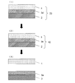
- a structure 10 includes a member 1, a base material 2 for supporting the member 1, and a temporary structure interposed between the member 1 and the base material 2.
- An adhesive 3 is provided.
- the temporary adhesive 3 includes at least a first temporary adhesive layer 3a.
- the first temporary adhesive layer 3a is obtained by curing the first curable composition layer of the present invention.
- the temporary adhesive 3 may further include a second temporary adhesive layer 3b (see FIG. 2).
- the temporary adhesive material 3 includes the second temporary adhesive material layer 3b, the first temporary adhesive material layer 3a is in contact with the member 1 and the second temporary adhesive material layer 3b, and the second temporary adhesive material layer 3b is in contact with the first temporary adhesive material layer 3b. It contacts the adhesive layer 3a and the substrate 2.
- the member 1 and the substrate 2 are bonded via a layer 3a ′ of the first curable composition.
- the laminated body 20 is formed by stacking.
- the layer 3a ′ of the first curable composition in the laminate 20 is irradiated with light having a wavelength of 400 nm or more to form the layer 3a ′ of the first curable composition. It hardens
- Various processes are performed on the member 1 of the temporary adhesive body (structure 10). After the processing, as shown in (3) of FIG. 3, at least the first temporary adhesive layer 3a is irradiated with light of less than 400 nm to peel the member 1 from the structure 10.
- the first curable composition layer 3a ′ is formed from the member 1 and the second temporary adhesive layer 3b.
- the first curable composition layer 3a ′ and the second temporary adhesive material so that the second temporary adhesive material layer 3b contacts the first curable composition layer 3a ′ and the substrate 2.
- the member 1 and the base material 2 are laminated via the layer 3b.
- the first curable composition layer 3a ′ of the laminate 20 is irradiated with light having a wavelength of at least 400 nm to form the first curable composition layer 3a ′.
- the first temporary adhesive layer 3a is cured to temporarily bond the member 1 and the substrate 2 via the first temporary adhesive layer 3a and the second temporary adhesive layer 3b. At this time, light irradiation with a wavelength of 400 nm or more may also be applied to the second temporary adhesive layer 3b.
- Various processes are performed on the member 1 of the temporary adhesive body (structure 10). After processing, as shown in (3) of FIG. 4, at least the first temporary adhesive layer 3 a is irradiated with light of less than 400 nm to peel the member 1 from the structure 10.
- the first curable composition of the present invention comprises a photopolymerizable group-containing silicone compound (A), a photopolymerization initiator that absorbs light in a wavelength region of 400 nm or more, and less than 400 nm.
- a photoacid generator that absorbs light in the wavelength region and at least one metal compound selected from the group consisting of metal carbonates, metal hydroxides, and metal oxides are included.
- composition of the first curable composition of the present invention is that the photopolymerization initiator is 0.01 to 10% by mass and the photoacid generator is 10 to 100% by mass with respect to the photopolymerizable group-containing silicone compound (A). %, And one or more metal compounds selected from the group consisting of metal carbonates, metal hydroxides and metal oxides are preferably 10 to 100% by mass.
- the photopolymerizable group-containing silicone compound (A) (hereinafter sometimes simply referred to as “silicone compound (A)”) is a silicone compound having a photopolymerizable group.
- This photopolymerizable group means a functional group that can be polymerized with a compound having silicone compounds (A) or other photopolymerizable groups by irradiation of light. Examples of such photopolymerizable groups include, but are not limited to, acryloyl groups and methacryloyl groups.
- the silicone compound (A) may have fluidity, and preferably has fluidity.
- the silicone compound (A) may have a 5% weight loss temperature (T d5 ) in a thermogravimetric analysis of 250 ° C. or higher depending on the material of the member and the temperature condition of the member processing during temporary bonding. What shows 280 degreeC or more is preferable.
- the silicone compound (A) include a cage silsesquioxane compound having an acryloyl group or a methacryloyl group, but are not limited thereto.
- a cage-type silsesquioxane compound represented by the following general formula (1) (hereinafter referred to as “ ⁇ -type silsesquioxane compound (1)”) May be included). Since this cage silsesquioxane compound (1) has fluidity, it can be suitably used.
- the L group represents an L 1 group or an L 2 group, the number of L 1 groups is 1 to 8, and the total of the L1 group and the L 2 group is 8.
- the L 1 group represents a monovalent organic group containing an acryloyl group or a methacryloyl group.
- the L 2 group represents a group inert to the photopolymerization initiator. When there are a plurality of L 1 groups and L 2 groups, they may be independently different.
- L 1 group examples include, but are not limited to, organic groups represented by the following formula (L-1).
- L-1 organic groups represented by the following formula (L-1).
- m represents an integer of 1 to 2
- p represents an integer of 1 to 3.
- R 1 represents a hydrogen atom or a methyl group.
- organic group represented by the formula (L-1) include the following organic groups.
- L 2 group examples include, but are not limited to, organic groups represented by the following formula (L-2-A) or formula (L-2-B).
- n represents an integer of 1 to 2
- q represents an integer of 2 to 5.
- organic group represented by the formula (L-2-A) or the formula (L-2-B) include the following organic groups.
- the cage silsesquioxane compound (1) may be used alone or in combination with a compound having a different L group. Further, in addition to these cage-type silsesquioxane compounds (1), cage-type silsesquioxane compounds represented by the following formula (2) (hereinafter referred to as “ ⁇ -type silsesquioxane compounds (2)”) An organosilicon compound such as may be used.
- L 3 group has the same meaning as L 2 group.
- the eight L 3 groups in the formula may be the same or different types.
- a composition containing at least an alkoxysilane compound represented by the general formula (3) (hereinafter sometimes referred to as “alkoxysilane compound (3)”) is hydrolyzed. And a hydrolytic condensate obtained by condensation (hereinafter sometimes referred to as “hydrolytic condensate (3)”).
- R 2 represents an organic group containing at least one group selected from the group consisting of an acryloyl group and a methacryloyl group
- R 3 is a methyl group or an ethyl group
- v is 1 to 3
- organic group containing at least one group selected from the group consisting of an acryloyl group and a methacryloyl group include, but are not limited to, a methacryloyloxyalkyl group and an acryloyloxyalkyl group.
- alkoxysilane compound (3) one type may be used, or a plurality of types may be used in combination. Specific examples include, but are not limited to: 3- (trimethoxysilyl) propyl methacrylate, 3- (triethoxysilyl) propyl methacrylate, 3- (trimethoxysilyl) propyl acrylate, 3- (triethoxysilyl) propyl acrylate, methacryloxymethyltriethoxysilane, methacryloxymethyl Trialkoxysilane compounds such as trimethoxysilane, (3-acryloxypropyl) methyldimethoxysilane, (methacryloxymethyl) methyldiethoxysilane, (methacryloxymethyl) methyldimethoxysilane, methacryloxypropylmethyldiethoxysilane, methacryloxy Dialkoxysilane compounds such as propylmethyldimethoxysilane; Monoalkoxysilane compounds such as methacryloxypropyldilane
- trialkoxysilane compounds are preferable, and specifically, 3- (trimethoxysilyl) propyl methacrylate is particularly preferable.
- the composition containing the alkoxysilane compound (3) may contain an alkoxysilane compound represented by the general formula (4) (hereinafter sometimes referred to as “alkoxysilane compound (4)”).
- the alkoxysilane compound (4) is hydrolytically condensed together with the alkoxysilane compound (3).
- physical properties such as heat resistance of the resulting hydrolysis condensate can be adjusted.
- R 4 represents a methyl group or a phenyl group, if R 4 there are a plurality, the plurality of R 4 may be the same or different type
- R 5 is a methyl group or an ethyl group represents, if R 5 there are a plurality, the plurality of R 5 may be the same or different type
- w is an integer of 0-3.
- alkoxysilane compound (4) one type may be used, or a plurality of types may be used in combination. Specific examples include, but are not limited to: Tetraalkoxysilane compounds such as tetramethoxysilane and tetraethoxysilane; trialkoxysilane compounds such as methyltrimethoxysilane, phenyltrimethoxysilane and phenyltriethoxysilane; Dialkoxysilane compounds such as dimethyldimethoxysilane, methylphenyldimethoxysilane, dimethyldiethoxysilane, diphenyldiethoxysilane, and methylphenyldiethoxysilane, and monoalkoxysilane compounds such as trimethylmethoxysilane.
- Tetraalkoxysilane compounds such as tetramethoxysilane and tetraethoxysilane
- trialkoxysilane compounds such as methyltrimethoxysilane
- trialkoxysilane compounds and dialkoxysilane compounds are preferable, and specifically, phenyltrimethoxysilane and dimethyldiethoxysilane are particularly preferable.
- a trialkoxysilane compound and a dialkoxysilane compound are preferably used in combination, and specifically, phenyltrimethoxysilane and dimethyldiethoxysilane are used in combination.
- the content is not particularly limited.
- the alkoxysilane compound (4) may be contained in an amount of 30 to 97 mol%, preferably 50 to 97 mol%, preferably 80 to 97%, based on the total amount of the alkoxysilane compound (3) and the alkoxysilane compound (4). Is particularly preferred.
- the mass average molecular weight of the hydrolysis-condensation product (3) is not particularly limited. 500 or more and 200,000 or less are preferable, More preferably, 500 or more and 100,000 or less are more preferable. If it is 500 or more, the temporary adhesive material of this invention can fully endure the process of the member mentioned later, and if it is 200000 or less, the composition of this invention will maintain fluidity
- the mass average molecular weight is a value obtained by measuring by a gel permeation chromatography method and converting by a standard polystyrene calibration curve (hereinafter, the same applies in the present specification).
- the manufacturing method of hydrolysis-condensation product (3) is not limited to this.
- the alkoxysilane compound (3) is mixed with water, a polymerization catalyst, optionally a reaction solvent, and optionally the alkoxysilane compound (4), followed by hydrolysis and condensation reaction.
- the hydrolysis condensate (3) can be obtained by performing.
- the polymerization catalyst is preferably an acid catalyst, and for example, acetic acid, hydrochloric acid and the like can be used.
- As the reaction solvent an alcohol can be suitably used. Among them, a lower alcohol is preferable, and isopropyl alcohol is particularly preferable.
- the reaction temperature is preferably 60 to 80 ° C., and the reaction time may be 6 to 24 hours.
- the hydrolysis condensate (3) may be purified by performing operations such as extraction, dehydration and solvent removal.
- Photopolymerization initiator As the photopolymerization initiator, a photopolymerization initiator that absorbs light in a wavelength region of 400 nm or more can be used. This photopolymerization initiator generates radicals when irradiated with light having a wavelength of 400 nm or longer, and the radicals act to start polymerization of the silicone compound (A). By this polymerization, the silicone compound (A) is polymerized and cured, and the fluidity of the first curable composition of the present invention is lost to form a cured film. The member and the substrate can be temporarily bonded via a temporary adhesive having at least a first temporary adhesive layer made of the cured film.
- the temporary adhesive material of this invention When the temporary adhesive material of this invention has a 1st temporary adhesive material layer and a 2nd temporary adhesive material layer, it is a silicone compound (A) in the interface of a 1st temporary adhesive material layer and a 2nd temporary adhesive material layer further. And a hydrolysis condensate (hereinafter referred to as “silicone compound (B)”) of a photopolymerizable group and hydrolyzable group-containing silicone compound (B) (hereinafter sometimes referred to as “silicone compound (B)”) contained in the second temporary adhesive layer. , Sometimes referred to as “hydrolysis condensate (B)”). Thereby, a 1st temporary adhesive material layer and a 2nd temporary adhesive material layer can be adhere
- photopolymerization initiator examples include, but are not limited to, the following compounds: Benzophenone, methyl orthobenzoin benzoate, 4-benzoyl-4'-methyldiphenyl sulfide, camphorquinone, 2-hydroxy-1- ⁇ 4- [4- (2-hydroxy-2-methylpropionyl) benzyl] phenyl ⁇ -2 -Methylpropan-1-one, 1-hydroxycyclohexyl phenyl ketone, 1- [4- (2-hydroxyethoxy) -phenyl] -2-hydroxy-2-methyl-1-propan-1-one), 2-benzyl -2-Dimethylamino-1- (4-morpholinophenyl) -butanone-1,2- (dimethylamino) -2-[(4-methylphenyl) methyl] -1- [4- (4-morpholinyl) phenyl ] 1-butanone, oxyphenylacetic acid and 2- [2-oxo-2-phenyl,
- examples of the photopolymerization initiator include, but are not limited to, the following Irgacure series manufactured by Ciba Specialty Chemicals Co., Ltd .: Irgacure 127, Irgacure 184, Irgacure 2959, Irgacure 369, Irgacure 379, Irgacure 379EG, Irgacure 907, Irgacure 1700, Irgacure 1800, Irgacure 1850, Irgacure 1850, Irgacure 1850, Irgacure 1850, Irgacure 1850, Irgacure 1850, Irgacure 1850, Irgacure 1850, Irgacure 1850, Irgacure 1850, Irgacure 1850, Irgacure 1850, Irgacure 1850, Irgacure 1850, Irg
- the content of the photopolymerization initiator in the first curable composition of the present invention is not particularly limited. It is preferable that it is 0.01 mass% or more and 10 mass% or less with respect to a silicone compound (A).
- the silicone compound (A) is favorably polymerized and cured by irradiation with light having a wavelength of 400 nm or more. Moreover, it is not necessary to add exceeding 10 mass%.
- Photoacid generator As the photoacid generator, a photoacid generator that absorbs light in a wavelength region of 400 nm or more can be used. This photoacid generator generates an acid when irradiated with light having a wavelength of less than 400 nm. As will be described later, the generated acid reacts with the metal compound contained in the first curable composition of the present invention to generate gas and water.
- the photoacid generator may have a 5% weight loss temperature (T d5 ) of 250 ° C. or higher in thermogravimetric analysis, depending on the material of the member and the temperature condition of the member processing during temporary bonding.
- T d5 can be determined by measuring from 25 ° C. at a rate of temperature increase of 10 ° C./min in the air atmosphere (the same applies hereinafter).
- Examples of the thermogravimetric analyzer include a differential thermothermal gravimetric apparatus (manufactured by Rigaku Corporation, model: Thermo Plus, TG8120).
- the type of photoacid generator is not particularly limited as long as it satisfies the above-described conditions.
- a photoacid generator of a triarylsulfonium salt and a nonionic photoacid generator can be used.
- ionic compounds such as triphenylsulfonium trifluoromethanesulfonate, triphenylsulfonium nonafluoro-n-butanesulfonate (manufactured by Midori Chemical Co., Ltd., trade name: TPS-109), NAI-101 (trade name, Midori) Nonionic compounds such as Chemical Co., Ltd. and NAI-100 (trade name, manufactured by Midori Chemical Co., Ltd.) and compounds having the following structures are preferred.
- the content of the photoacid generator in the first curable composition of the present invention is not particularly limited. It is preferable that it is 10 mass% or more with respect to a silicone compound (A). If it is 10 mass% or more, gas and water will fully generate
- metal compounds As the metal compound, one or more metal compounds selected from the group consisting of metal carbonates, metal oxides and metal oxides can be used. Examples of such metal compounds include, but are not limited to, the following metal carbonates, metal oxides, and metal hydroxides.
- Metal carbonate lithium carbonate (Li 2 CO 3 , melting point: 723 ° C.), sodium carbonate (Na 2 CO 3 , melting point: 851 ° C.), potassium carbonate (K 2 CO 3 , melting point: 891 ° C.), rubidium carbonate (Rb 2 CO 3 , melting point: 837 ° C.), cesium carbonate (Cs 2 CO 3 , melting point: 610 ° C.), calcium carbonate (Ca 2 CO 3 , melting point: 825 ° C.), barium carbonate (BaCO 3 , melting point: 811 ° C.), Magnesium carbonate (MgCO 3 , melting point: 350 ° C.), strontium carbonate (SrCO 3 , melting point: 1497 ° C.), cobalt carbonate (CoCO 3 ).
- Metal oxide lithium oxide (Li 2 O, melting point: 1570 ° C.), sodium oxide (Na 2 O, melting point: 1132 ° C.), potassium oxide (K 2 O, melting point: 350 ° C.), beryllium oxide (BeO, melting point: 2570 ° C.), magnesium oxide (MgO, melting point: 2800 ° C.), calcium oxide (CaO, melting point: 2613 ° C.), titanium dioxide (TiO 2 , melting point: 1870 ° C.), dichromium trioxide (Cr 2 O 3 , melting point: 2435 ° C.), manganese dioxide (MnO 2 , melting point: 535 ° C.), ferric trioxide (Fe 2 O 3 , melting point: 1566 ° C.), triiron tetroxide (Fe 3 O 4 , melting point: 1597 ° C.), cobalt oxide (CoO, mp: 1933 ° C.), nickel oxide (NiO, mp: 1984 ° C.), copper oxide
- Metal hydroxide lithium hydroxide (LiOH, melting point: 462 ° C.), sodium hydroxide (NaOH, melting point: 318 ° C.), potassium hydroxide (KOH, melting point: 360 ° C.), magnesium hydroxide (Mg (OH) 2 , Melting point: 350 ° C.), calcium hydroxide (Ca (OH) 2 , melting point: 580 ° C.), strontium hydroxide (Sr (OH) 2 , melting point: 375 ° C.), barium hydroxide (Ba (OH) 2 , melting point : 408 ° C.), iron hydroxide (Fe (OH) 2 , melting point: 350 to 400 ° C.).
- metal compounds having a relatively small molecular weight are preferably used, and lithium carbonate, sodium carbonate, potassium carbonate, calcium carbonate, magnesium carbonate, lithium oxide, sodium oxide, potassium oxide, beryllium oxide, magnesium oxide, calcium oxide, water Lithium oxide, sodium hydroxide, potassium hydroxide, magnesium hydroxide, calcium hydroxide and the like are preferable, and lithium carbonate, sodium carbonate, potassium carbonate, lithium oxide, magnesium oxide, lithium hydroxide, and calcium hydroxide are particularly preferable.
- This metal compound easily reacts with the protonic acid generated from the photoacid generator to generate gas and / or water.
- the metal compound when lithium carbonate and lithium hydroxide are used as the metal compound and trifluoromethanesulfonic acid is used as the proton acid, carbon dioxide and water are generated according to the following reaction formulas. Generation
- a material having a melting point of 250 ° C. or higher may be used depending on the material of the member or the temperature condition of the member processing at the time of temporary bonding, and a material showing 280 ° C. or higher is preferable.
- the content of the metal compound in the first curable composition of the present invention is not particularly limited. It is preferable that it is 10 mass% or more with respect to a silicone compound (A). If it is 10 mass% or more, the acid and metal compound which generate
- the average particle size of the metal compound is preferably 10 ⁇ m or less, and the lower limit is not particularly limited.
- the maximum particle diameter is preferably 30 ⁇ m or less, and the lower limit is not particularly limited. If the average particle diameter is 10 ⁇ m or less, damage to the member can be suppressed. Moreover, if the maximum particle diameter is 30 micrometers or less, the smoothness and uniformity of the temporary adhesive material of this invention can be kept favorable. More preferable particle diameters are an average particle diameter of 1 ⁇ m or less and a maximum particle diameter of 5 ⁇ m or less.
- the average particle diameter of the metal compound is the average value when the major axis is measured by selecting any 20 particles from an observation image with a magnification of 100,000 using a scanning electron microscope (abbreviation: SEM). means.
- the 1st curable composition may contain the compound which has a polar group as an additive for the purpose of the improvement and adjustment of the adhesive force of the temporary adhesive material and member of this invention.
- a polar group A hydroxyl group, a carboxylic acid group, a silanol group, a phosphoric acid group etc. are mentioned.
- a compound having one or more polar groups and one or more photopolymerizable groups is preferable. Specifically, methacrylic acid (2-hydroxyethyl) (abbreviation: HEMA) is used.
- HEMA is particularly preferably used.
- the first curable composition may contain a compound having two or more photopolymerizable groups as an additive for the purpose of improving the crosslink density by the photopolymerizable group.
- a tougher cured film can be obtained.
- Specific examples of such compounds include ethylene glycol diacrylate, ethylene glycol dimethacrylate, neopentyl glycol diacrylate, pentaerythritol tetraacrylate, dipentaerythritol hexaacrylate, and trimethylolpropane triacrylate (abbreviation: TMPTA).
- TMPTA trimethylolpropane triacrylate
- TMPTA trimethylolpropane triacrylate
- the content of the additive in the first curable composition is preferably 1% by mass or more and 30% by mass or less with respect to the silicone compound (A). If it is 1 mass% or more, adhesive force and a crosslinking density can be improved, and it is not necessary to add exceeding 50 mass%. Especially preferably, it is 10 mass% or more and 20 mass% or less.
- the first curable composition may contain a filler such as silica or alumina for the purpose of adjusting the thermal expansion coefficient.
- a filler such as silica or alumina for the purpose of adjusting the thermal expansion coefficient.
- the average particle diameter is preferably 10 ⁇ m or less, and the lower limit is not particularly limited.
- the maximum particle size is preferably 30 ⁇ m or less, and the lower limit is not particularly limited. If the average particle diameter is 10 ⁇ m or less, damage to the member can be suppressed. Moreover, if the maximum particle diameter is 30 micrometers or less, the smoothness and uniformity of the temporary adhesive material of this invention can be kept favorable. More preferable particle diameters are an average particle diameter of 1 ⁇ m or less and a maximum particle diameter of 5 ⁇ m or less.
- the average particle diameter of the filler means an average value when a major axis is measured by selecting 20 arbitrary particles from an observation image with a magnification of 100,000 times using a scanning electron microscope (abbreviation: SEM). To do.
- SEM scanning electron microscope
- the particle shape of the filler is preferably spherical because it is well mixed with the components of the first curable composition.
- the first curable composition is preferably mixed and kneaded.
- the dispersion state of the metal compound and photoacid generator in the first curable composition can be improved, and the reproducibility of temporary adhesion and peeling can be improved.
- the kneading is performed using an apparatus such as a stirring deaerator, a mortar, a homogenizer, a roll mill, or a kneader.
- the first curable composition Since the first curable composition has fluidity, even if the surface of the member is processed into a fine shape (unevenness), it can follow the fine shape (unevenness). Therefore, when the first curable composition applied to the member is temporarily bonded as a cured film by irradiation with light having a wavelength of 400 nm or more, the entrapment of bubbles on the temporary bonding surface between the cured film and the member is performed. And can sufficiently withstand the processing of the member.
- Temporary adhesive The temporary adhesive of the present invention includes at least a first temporary adhesive layer made of a cured film of the first curable composition.
- the cured film of the first curable composition can be obtained by irradiating light having a wavelength of 400 nm or more onto the layer of the first curable composition obtained by applying the first curable composition to a member or a substrate.
- the first curable composition Since the first curable composition has fluidity, it can be applied to a member or a substrate without being dissolved in a solvent. Therefore, heat treatment such as pre-baking can be omitted.
- a solvent may be used for application to a member or a substrate.
- the first curable composition is dissolved in the solvent and applied as a solution (hereinafter sometimes referred to as “(A) solution”) to the member or the substrate.
- (A) solution After application
- the coating film is cured to form a cured film (first temporary adhesive layer) of the first curable composition.
- the member and the substrate can be temporarily bonded to each other.
- the type of the solvent to be used may be appropriately selected in consideration of the solubility of the first curable composition, the material of the member and the base material, and the like.
- examples include isopropyl alcohol, propylene glycol methyl ether acetate (abbreviation: PGMEA), propylene glycol monomethyl ether (abbreviation: PGMEA), methyl isobutyl ketone (abbreviation: MIBK), methyl ethyl ketone (abbreviation: MEK), and the like.
- solvents may be used alone or in combination of two or more.
- the method for applying the solution is not particularly limited as long as the method can form a flat thin film on the substrate.
- a spin coating method for example, a spin coating method, a dip coating method, a bar coating method, a roll coating method, a die coating method, or a slit coating method can be employed.
- the first curable composition as it is without using a solvent, a dispenser, screen printing, or the like can be employed in addition to the above application method.
- the temporary adhesive material of the present invention can also be used as a temporary adhesive material for wafer processing described later.
- the temporary adhesive of the present invention contains at least a hydrolysis condensate of a photopolymerizable group- and hydrolyzable group-containing silicone compound (B) (hereinafter sometimes referred to as “silicone compound (B)”). You may provide the 2nd temporary adhesive material layer which consists of a film
- the second temporary adhesive layer may be formed as a film on the layer of the first curable composition or may be formed as a film on the base material when the member and the base material are temporarily bonded.
- the second temporary adhesive layer may be formed by previously forming a second temporary adhesive layer on the base material by applying a film of the second curable composition to the base material when the member and the base material are temporarily bonded. Well, it is preferable to do so.
- the film of the second curable composition is dissolved in a solvent and applied to the substrate as a solution (hereinafter sometimes referred to as “(B) solution”).
- (B) solution After application
- the kind of the solvent that can be used at this time may be selected in consideration of the fact that the film of the second curable composition is soluble, the material of the member and the substrate, and the like.
- PGMEA propylene glycol 1-monomethyl ether 2-acetate
- PGMEA propylene glycol monomethyl ether
- These solvents may be used alone or in combination of two or more.
- the second curable composition is further subjected to heat treatment at 80 to 250 ° C. after pre-baking. This film may be further cured.
- the method of applying the solution is not particularly limited as long as a flat thin film can be formed on the substrate.
- Specific examples include spin coating, dip coating, bar coating, roll coating, die coating, and slit coating.
- spin coating method which is generally used in a semiconductor process and can obtain good flatness on a coated surface.
- the thickness of the second temporary adhesive layer is not particularly limited as long as it can withstand each operation according to the present invention, that is, temporary bonding of the member and the base material, processing of the member, and operation of separating the member and the base material. Although it varies depending on the type of member or substrate, the type of processing, etc., it is usually preferably 0.5 to 500 ⁇ m, particularly preferably 0.5 to 200 ⁇ m. Further, as described above, the thickness of the temporary adhesive material of the present invention is preferably 1 to 1000 ⁇ m, preferably 1 to 400 ⁇ m, including the first temporary adhesive material layer and the second temporary adhesive material layer. Particularly preferred.
- the second curable composition contains at least a hydrolysis condensate of the silicone compound (B) (hereinafter sometimes referred to as “hydrolysis condensate (B)”).
- the photopolymerizable group of the silicone compound (B) means a functional group that can be polymerized with the photopolymerizable group-containing silicone compound (A) or another compound having a photopolymerizable group by irradiation with light. To do.
- photopolymerizable groups include, but are not limited to, acryloyl groups and methacryloyl groups.
- hydrolyzable group of the silicone compound (B) include an alkoxy group and a chlorine atom.
- the silicone compound (B) may have a 5% weight loss temperature (Td5) in a thermogravimetric analysis of 250 ° C. or higher depending on the material of the member and the temperature condition of the member processing during temporary bonding. What shows more than degreeC is preferable.
- the mass average molecular weight of the hydrolysis-condensation product (B) is not particularly limited. 500 or more and 200,000 or less are preferable, and 500 or more and 100,000 or less are more preferable. If it is 500 or more, it can fully endure the process of the member mentioned later, and if it is 200,000 or less, removal of a temporary adhesive material from the member and base material after peeling mentioned later is easy.
- alkoxysilane compound (5) As a specific example of the hydrolysis condensate (B), an alkoxysilane compound represented by the following general formula (5) (hereinafter sometimes referred to as “alkoxysilane compound (5)”) is hydrolyzed and condensed. Although the hydrolysis-condensation product obtained is mentioned, it is not limited to this.
- R 6 represents an organic group containing at least one group selected from the group consisting of acryloyl group and methacryloyl group, if R 6 there is a plurality, the plurality of R 6 same or different types may also be, R 7 is a methyl or ethyl group, if R 7 there is a plurality, the plurality of R 7 may be the same or different types, s is an integer of 1-3.
- organic group containing at least one group selected from the group consisting of an acryloyl group and a methacryloyl group include, but are not limited to, a methacryloyloxyalkyl group and an acryloyloxyalkyl group.
- alkoxysilane compound (5) one type may be used, or a plurality of types may be used in combination. Specifically, the same kind as the specific example of the alkoxysilane compound (3) is mentioned. Of these, trialkoxysilane compounds and dialkoxysilane compounds are preferred, and specifically, 3- (trimethoxysilyl) propyl methacrylate is particularly preferred.
- the hydrolysis-condensation product (B) is an alkoxysilane compound (5) and an alkoxysilane compound represented by the following general formula (6) (hereinafter, sometimes referred to as “alkoxysilane compound (6)”). Hydrolysis condensates obtained by hydrolytic condensation using at least one of each may be used. By using the alkoxysilane compound (6) together with the alkoxysilane compound (5), physical properties such as heat resistance of the resulting hydrolysis condensate can be adjusted.
- R 8 is a methyl group or a phenyl group, if R 8 there are a plurality, the plurality of R 8 may be the same or different type, R 9 is a methyl group or an ethyl group There, if R 9 there are a plurality, a plurality of R 9 may be the same or different type, t is an integer of 0-3.
- alkoxysilane compound (6) may be used, or a plurality of types may be used in combination. Specific examples include the same types as those given as specific examples of the alkoxysilane compound (4). Of these, trialkoxysilane compounds and dialkoxysilane compounds are preferable, and phenyltrimethoxysilane and dimethyldiethoxysilane are particularly preferable.
- a trialkoxysilane compound and a dialkoxysilane compound are preferably used in combination, and specifically, phenyltrimethoxysilane and dimethyldiethoxysilane are used in combination.
- the amount used is not particularly limited.
- the alkoxysilane compound (6) is preferably used in an amount of 3 to 50 mol%, particularly preferably 3 to 20 mol%, based on the total amount of the alkoxysilane compound (5) and the alkoxysilane compound (6).
- the alkoxysilane compound (5) is mixed with water, a polymerization catalyst, optionally a reaction solvent, and optionally the alkoxysilane compound (6), and then subjected to hydrolysis and condensation reaction.
- the hydrolysis condensate (B) can be obtained.
- the polymerization catalyst is preferably an acid catalyst, and for example, acetic acid, hydrochloric acid and the like can be used.
- As the reaction solvent an alcohol can be suitably used, preferably a lower alcohol, and particularly preferably isopropyl alcohol.
- the reaction temperature is preferably 60 to 80 ° C., and the reaction time may be 6 to 24 hours.
- the hydrolysis condensate (B) may be purified by performing operations such as extraction, dehydration and solvent removal.
- the second curable composition may contain a photopolymerization initiator.
- a photopolymerization initiator By including a photopolymerization initiator, chemical irradiation can be efficiently formed in a wider range between the first curable composition and the second temporary adhesive layer by irradiation with light having a wavelength of 400 nm or more during temporary bonding. It is possible to expect strong adhesion.
- the same type of photopolymerization initiator as exemplified as the photopolymerization initiator contained in the first curable composition can be used.
- the content of the photopolymerization initiator in the second curable composition may be 0.01 to 5% by mass or less based on the hydrolysis condensate (B).
- the 2nd curable composition may contain fillers, such as a well-known antioxidant and a silica. By including a filler, the heat resistance can be further increased.
- the structure of the present invention is formed by temporarily bonding a member and a substrate through the temporary adhesive of the present invention.
- the member and the substrate can be temporarily bonded according to a method for temporarily bonding the member and the substrate described later.
- the member to be used is not particularly limited.
- a crystal member, a glass member, a plastic member, a semiconductor wafer, or the like can be used. Therefore, the temporary bonding method of the present invention can be applied to temporary bonding in processing of a crystal resonator, a glass lens, a plastic lens, an optical disk, a semiconductor wafer, and the like.
- examples of the type include a silicon wafer, a germanium wafer, a gallium-arsenic wafer, a gallium-phosphorus wafer, a gallium-arsenic-aluminum wafer, a gallium nitride wafer, and silicon carbide.
- Some of these semiconductor wafers may be preliminarily ground, polished, processed, or may be coated with a protective film (permanent film).
- the member used may have a fine structure (uneven structure) on its surface. Since the first curable composition used in the method for temporarily bonding a member and a substrate of the present invention has fluidity, even if the surface of the member has a fine structure (uneven structure), the first curable composition is used. The composition follows it. As a result, when the first curable composition is cured and the member and the base material are temporarily bonded as a temporary adhesive, temporary bonding can be performed without entrapment of bubbles between the member and the adhesive. It can sufficiently withstand the subsequent processing of the member. Therefore, the method for temporarily bonding a member and a substrate of the present invention is particularly useful when a member having a fine structure (uneven surface) is used.
- the thickness of the member used is not particularly limited.
- a semiconductor wafer when used as the member, it may typically be 200 to 1000 ⁇ m, more typically 625 to 775 ⁇ m.
- ⁇ Base material> There is no restriction
- transmit is preferable.
- the material of the base material include a crystal base material, a glass base material, and a plastic base material, but are not limited thereto, and the material may be appropriately selected according to the light source to be used.
- any of soda lime glass, alkali-free glass, borosilicate glass, aluminosilicate glass, fused quartz glass, and synthetic quartz glass may be used. Moreover, you may use that whose alkali element content in a glass base material is 1 mass% or less as a glass base material. Specific examples of such a glass substrate include alkali-free glass, fused silica glass, and synthetic quartz glass. Among these, alkali-free glass is preferable from the viewpoint of availability.
- the material of the barrier film is not particularly limited as long as the barrier performance is exhibited, and SiO 2 is preferable from the viewpoint of adhesiveness.
- This barrier film can be produced by a technique such as vacuum deposition, sputtering, thermal decomposition film formation, or sol-gel method.
- the surface to be bonded to the temporary adhesive in the substrate in advance polishing treatment such as ceria polishing, zirconia polishing, alumina polishing, washing with an acidic aqueous solution, It is preferable to perform cleaning using a basic aqueous solution, cleaning using a surfactant, cleaning using ozone water, UV ozone irradiation processing, plasma irradiation processing, or substrate cleaning using a combination thereof.
- polishing treatment such as ceria polishing, zirconia polishing, alumina polishing, washing with an acidic aqueous solution.
- cleaning treatment such as ceria polishing, zirconia polishing, alumina polishing, washing with an acidic aqueous solution
- cleaning using a basic aqueous solution cleaning using a surfactant
- cleaning using ozone water cleaning using ozone water
- UV ozone irradiation processing cleaning using ozone water
- plasma irradiation processing or substrate cleaning using a combination thereof.
- the material of the base material to be used may be appropriately selected according to the material of the member.
- the material of the member can transmit light having a wavelength of 400 nm or more
- the material of the base material is preferably a material that can transmit at least light having a wavelength of less than 400 nm, and the material of the member transmits light having a wavelength of less than 400 nm.
- the base material is preferably a material that can transmit at least light having a wavelength of 400 nm or more.
- Temporary Bonding Method Between Member and Substrate includes the following first to fourth steps.
- 2nd process The process of obtaining the structure formed by irradiating and hardening the light of wavelength 400nm or more to the temporary adhesive material before a hardening process, and temporarily bonding a member and a base material.
- 3rd process The process of processing the member of a structure.
- Fourth step A step of peeling the member from the structure by irradiating light having a wavelength of less than 400 nm to the temporary adhesive after the curing treatment in the processed structure.
- the temporary bonding method between the member and the substrate of the present invention may further include the following sixth step and seventh step.
- 6th process The process of removing the residue of the temporary adhesive material after the hardening process which remains on the base material after peeling.
- Seventh step A step of reusing the base material obtained in the sixth step in the first step.
- the temporary adhesive material after the curing treatment does not remain on the member after the fourth step, or even if it remains. If necessary, the following fifth step may be included after the fourth step. 5th process: The process of removing the residue of the temporary adhesive material after the hardening process which remains in the peeled member.
- a member and a base material are laminated
- the temporary adhesive material before the curing treatment may further include a second temporary adhesive material layer.
- the first curable composition layer is divided into the member and the second temporary adhesive material layer.
- the second temporary adhesive layer is contacted and laminated so as to contact the first curable composition layer and the substrate. That is, the member, the first curable composition layer, the second temporary adhesive layer and the base material are laminated in this order.
- the temporary adhesive material prior to the curing treatment is irradiated with light having a wavelength of 400 nm or more to be cured, and a structure formed by temporarily bonding the member and the base material is obtained.
- a 1st temporary adhesive material layer and a 2nd temporary adhesive material layer can be adhere
- the hydrolyzed condensate (B) may be further polymerized and cured. Thereby, the adhesive strength of a 2nd temporary adhesive layer and a base material can be improved.
- a method for irradiating the temporary adhesive forming layer with light having a wavelength of 400 nm or more is not particularly limited.
- the temporary adhesive before the curing treatment may be directly irradiated with light, or from the viewpoint of light irradiation efficiency, as described above, a base material or member having a material that can transmit light with a wavelength of 400 nm or more is used. It is preferable to irradiate the temporary adhesive before the curing treatment from the substrate side or the member side. Irradiation time is not particularly limited as long as the member and the substrate can be bonded via the temporary adhesive, and when the temporary adhesive before the curing treatment includes the second temporary adhesive layer, the first temporary adhesive is further provided.
- the light source is not particularly limited as long as it can irradiate light having a wavelength of 400 nm or more, but it is preferable that the light source has a wavelength less than 400 nm or does not include at all.
- a blue LED having a central wavelength of 405 nm, a 420 nm LED, a 465 nm LED, a 595 nm LED, and the like can be used, but the present invention is not limited to these.
- the integrated quantity of light wavelength 400nm or more light but are not particularly limited, 1 ⁇ 300,000mJ / cm 2, preferably 10 ⁇ 30,000mJ / cm 2 or less.
- the accumulated light quantity can be measured using, for example, a commercially available illuminometer (manufactured by USHIO INC., Body model number: UIT-201, light receiving unit model number: UVD-405PD, etc.).
- the member in the structure obtained in the second step is processed.
- a desired process can be given according to the member to be used and a use.
- desired machining such as cutting, polishing, grinding, surface protection, and drilling is performed.
- electrode forming processing, metal wiring forming processing, protective film forming processing Etc. are included in this processing.
- metal sputtering for forming electrodes, etc. wet etching for etching a metal sputtering layer, application of a resist to form a mask for forming a metal wiring, pattern formation by exposure and development, resist peeling
- wet etching for etching a metal sputtering layer
- resist peeling Also known processes such as dry etching, metal plating, silicon etching for TSV formation, and oxide film formation on the silicon surface.
- the temporary adhesive after the curing process in the processed structure is irradiated with light having a wavelength of less than 400 nm to peel the processed member from the structure.
- a method of irradiating the temporary adhesive after the curing treatment with light having a wavelength of less than 400 nm at a predetermined temperature for a predetermined time is used.
- an acid is generated from the photoacid generator contained in the first temporary adhesive layer, and gas and water are generated by the reaction of this acid with the metal compound contained in the first temporary adhesive layer.
- the processed member can be easily peeled from the structure by the internal stress due to the generation of gas or water.
- the member and base material after a process are separable.
- the temperature at which light irradiation with a wavelength of less than 400 nm is performed is not particularly limited as long as it does not adversely affect the workpiece obtained by processing the member in the third step. Peeling becomes easier by volatilizing the generated water, and therefore, it is preferable to carry out under a temperature condition of 100 ° C. or higher. Or you may make it peel by heating after irradiating light with a wavelength of less than 400 nm, and promoting a chemical reaction. In this case, for example, after light irradiation with a wavelength of less than 400 nm is performed at room temperature, the film is further heated and peeled off. In any case, the member can be easily peeled off from the processed structure due to internal stress due to generation of gas or water.
- the temporary adhesive after the curing treatment may be directly irradiated with light, or from the viewpoint of light irradiation efficiency, as described above, a base made of a material that can transmit light with a wavelength of less than 400 nm. It is preferable to use a material or member to irradiate light from the base material side or member side to the temporary adhesive after the curing treatment.
- the irradiation time of light having a wavelength of less than 400 nm is not particularly limited as long as the processed member can be peeled from the structure. Usually, the film is peeled off with an irradiation time of about 5 seconds to 10 minutes, but this irradiation time may be appropriately adjusted.
- the light source is not particularly limited as long as it can emit light having a wavelength of less than 400 nm.
- Specific examples include low-pressure mercury lamps, high-pressure mercury lamps, short arc discharge lamps, and ultraviolet light-emitting diodes, which are known ultraviolet lamps.
- a high-pressure mercury lamp belonging to a high-pressure discharge lamp, a metal halide lamp, or a xenon lamp belonging to a short arc discharge lamp can be used depending on the light amount and wavelength suitable for the photoacid generator to be used.
- the integrated quantity of light of wavelength less than 400nm light but are not particularly limited, 300 J / cm 2 or less, preferably 30 J / cm 2 or less.
- the accumulated light quantity can be measured using, for example, a commercially available illuminometer (manufactured by USHIO INC., Main unit model number UIT-201, light receiving unit model number UVD-365PD, etc.).
- organic solvents can be used: Isopropanol, PGMEA, PGME, MEK, hexane, toluene, N-methylpyrrolidone, acetone and the like. These organic solvents may be used singly or in combination of two or more. Moreover, it is good also as a mixed solution which added bases and acids to these organic solvents. These bases and acids may be aqueous solutions. Moreover, the existing surfactant can also be added to these organic solvents.
- the cleaning method a method of cleaning with a paddle using the organic solvent, a method of cleaning by spraying, a method of immersing in a cleaning liquid tank, and the like are possible.
- the temperature is usually 20 ° C. or more and 100 ° C. or less, and preferably 20 ° C. or more and less than 50 ° C. If necessary, it is possible to obtain a processed member by dissolving the temporary adhesive after curing with these dissolving solutions, and finally rinsing with water or rinsing with alcohol and drying.
- the residue of the temporary adhesive after the curing treatment adheres to the substrate side almost entirely or completely.
- the temporary adhesive residue after these curing treatments is removed from the substrate.
- the removal of the residue of the temporary adhesive after the curing treatment can be performed, for example, by washing the base material.
- the cleaning method is not particularly limited as long as the residue of the temporary adhesive after the curing treatment can be removed from the base material.
- the base material after the residue removal is reused in the first step, the base material is not adversely affected. It is preferable to adopt the method.
- the cleaning method described in the fifth step the base cleaning method and the acid cleaning method described later can be employed, and the base cleaning method and the acid cleaning method are preferably employed.
- Base washing method In the base washing method, the substrate is washed with a mixed washing solution comprising a tetraalkylammonium hydroxide having 1 to 4 carbon atoms in the alkyl group, an alcohol having 1 to 5 carbon atoms and N-methylpyrrolidone.
- the composition ratio of the mixed cleaning liquid is preferably such that the composition ratio of the tetraalkylammonium hydroxide, the alcohol, and the N-methylpyrrolidone is in the range of 1 to 20:20 to 98: 1 to 79.
- the cleaning method for example, a dip type cleaning in which the substrate is immersed in a dip tank containing the mixed cleaning solution, a showering method in which the mixed cleaning solution is sprayed by a shower, a spray, and / or a jet, a sponge or a brush is used.
- a scrub cleaning method in which the mixed cleaning solution is sprayed by a shower, a spray, and / or a jet, a sponge or a brush
- Examples include a scrub cleaning method, an ultrasonic cleaning method in which ultrasonic waves are applied to immersion cleaning to increase cleaning efficiency, and a bubbling cleaning method.
- the temperature of the mixed cleaning liquid upon contact with the substrate is preferably 20 to 120 ° C, more preferably 40 to 100 ° C.
- the substrate is cleaned with a cleaning solution containing sulfuric acid and hydrogen peroxide (SPM cleaning) or with a mixed cleaning solution of hydrochloric acid, hydrogen peroxide and ultrapure water (HPM cleaning), and then an aqueous nitric acid solution. Is washed with nitric acid (washed with nitric acid), finally washed with water, and then dried.
- SPM cleaning sulfuric acid and hydrogen peroxide
- HPM cleaning mixed cleaning solution of hydrochloric acid, hydrogen peroxide and ultrapure water
- the SPM cleaning is performed by heating a cleaning solution containing sulfuric acid and hydrogen peroxide.
- the washing conditions are not particularly limited, a commonly used composition having a volume ratio of sulfuric acid to hydrogen peroxide of 4: 1 to 8: 1 and a washing temperature of 80 to 150 ° C. is sufficient.
- the HPM cleaning is performed by heating a mixed cleaning solution of hydrochloric acid, hydrogen peroxide, and ultrapure water.
- the washing conditions are not particularly limited, the composition commonly used is a volume ratio of hydrochloric acid, hydrogen peroxide and ultrapure water ranging from 1: 1: 5 to 1: 4: 10, and the washing temperature is from 50 to 100 ° C is sufficient.
- the nitric acid cleaning is preferably performed using an aqueous solution having a nitric acid concentration in the range of 1 to 60% by mass, more preferably in the range of 10 to 40% by mass.
- the washing temperature is not particularly limited but is preferably 20 to 100 ° C, more preferably 40 to 90 ° C.
- the base material that has undergone the sixth step can be reused as the base material in the first step.
- the temporary adhesive material for wafer processing of the present invention has a circuit forming surface on the front surface, and temporarily attaches the wafer having the back surface to be processed to the support. It is a temporary adhesive for wafer processing interposed between bodies.
- the temporary adhesive material of the present invention described above is used as the temporary adhesive material for wafer processing.
- the wafer can be the same type as the semiconductor wafer exemplified as the material of the above-mentioned member, and the support is the same type as the glass substrate exemplified as the material of the above-mentioned base material. Can be used.
- Temporary bonding method between wafer and support is a temporary bonding method between a wafer and a support having a circuit forming surface on the surface and a back surface to be processed. At least the steps (a) to (d) are included.
- the method for temporarily bonding the wafer and the support of the present invention may further include the following steps (f) and (g).
- the temporary adhesive for wafer processing after the curing process does not remain on the surface of the wafer after the step (d), or even if it remains. If necessary, the following step (e) may be included after the step (d). Step (e): A step of removing a residue of the temporary adhesive for wafer processing after the curing process remaining on the surface of the peeled wafer.
- a curing treatment including at least a layer of the first curable composition of the present invention, which has a circuit forming surface on the surface is in contact with the surface of the wafer having the back surface to be processed, and is in contact with the support.
- the wafer and the support are laminated via the previous temporary adhesive for wafer processing.
- the temporary adhesive for wafer processing before the curing treatment may further include a second temporary adhesive layer, and in this case, the first curable composition layer is formed between the surface of the wafer and the second temporary adhesive material layer.
- the second temporary adhesive layer is laminated so as to contact the first curable composition layer and the support. That is, the wafer, the first curable composition layer, the second temporary adhesive layer and the support are laminated in this order.
- Step (b) In the step (b), a wafer processing structure formed by irradiating a temporary processing adhesive for wafer processing with a light having a wavelength of 400 nm or more to cure and temporarily bonding the surface of the wafer and the support. Get.
- Step (b) can be described by applying the explanation of the second step described above. That is, the temporary adhesive material before the curing process, the temporary adhesive material after the curing process, the member, the base material, and the structure in the explanation of the second step described above are respectively the temporary adhesive for wafer processing before the curing process, and after the curing process. This can be explained by replacing it with a temporary adhesive for wafer processing, a wafer surface, a support, and a wafer processing structure.
- Step (c) is a step of processing the back surface of the wafer in the wafer processing structure obtained in step (b).
- a desired process can be given.
- a thin wafer manufacturing process in which the back surface of the wafer is ground or polished to reduce the thickness of the wafer, an electrode forming process, a metal wiring forming process, a protective film forming process, and the like are included in this process. .
- metal sputtering for forming electrodes, etc. wet etching for etching a metal sputtering layer, application of a resist to form a mask for forming a metal wiring, pattern formation by exposure and development, resist peeling
- wet etching for etching a metal sputtering layer
- resist peeling Also known processes such as dry etching, metal plating, silicon etching for TSV formation, and oxide film formation on the silicon surface.
- the processed wafer processing structure is irradiated with light having a wavelength of less than 400 nm on the post-curing wafer processing temporary adhesive to peel the processed wafer from the wafer processing structure.
- a method of irradiating light having a wavelength of less than 400 nm at a predetermined temperature for a predetermined time on the temporary adhesive for wafer processing after the curing treatment is used.
- an acid is generated from the photoacid generator contained in the first temporary adhesive layer, and gas and water are generated by the reaction of this acid with the metal compound contained in the first temporary adhesive layer.
- the processed wafer Due to the internal stress due to the generation of gas and water, the processed wafer can be easily peeled from the processed wafer processing structure. Thereby, the processed wafer and the support can be separated.
- the method for peeling the processed wafer from the processed wafer processing structure after the light irradiation treatment is not particularly limited. For example, a method in which the processed wafer and support are slid in the opposite direction along the horizontal method to separate them, one of the processed wafer and support is fixed horizontally, and the other from the horizontal direction. For example, a method of lifting at a certain angle.
- the temperature at which light irradiation with a wavelength of less than 400 nm is performed is not particularly limited as long as it does not adversely affect the workpiece obtained by processing the back surface of the wafer in step (c). Peeling becomes easier by volatilizing the generated water, and therefore, it is preferable to carry out under a temperature condition of 100 ° C or higher. Or you may make it peel by heating after irradiating light with a wavelength of less than 400 nm, and promoting a chemical reaction. In this case, for example, after light irradiation with a wavelength of less than 400 nm is performed at room temperature, the film is further heated and peeled off.
- the wafer can be easily peeled off from the processed wafer processing structure by internal stress due to generation of gas or water.
- the temporary adhesive for wafer processing after the curing treatment may be directly irradiated with light, or from the viewpoint of light irradiation efficiency, a support made of a material that can transmit light with a wavelength of less than 400 nm is used. It is preferable to irradiate the temporary adhesive for wafer processing after the curing treatment from the support side.
- the irradiation time of light having a wavelength of less than 400 nm is not particularly limited as long as the processed wafer can be peeled from the wafer processing structure.
- the film is peeled off with an irradiation time of about 5 seconds to 10 minutes, but this irradiation time may be appropriately adjusted. From the viewpoint of efficiency, a shorter irradiation time is preferable.
- the light source is not particularly limited as long as it can emit light having a wavelength of less than 400 nm. Specific examples include low-pressure mercury lamps, high-pressure mercury lamps, short arc discharge lamps, and ultraviolet light-emitting diodes, which are known ultraviolet lamps. In addition, a high-pressure mercury lamp belonging to a high-pressure discharge lamp, a metal halide lamp, or a xenon lamp belonging to a short arc discharge lamp can be used depending on the light amount and wavelength suitable for the photoacid generator to be used.
- the integrated quantity of light of wavelength less than 400nm light but are not particularly limited, 300 J / cm 2 or less, preferably 30 J / cm 2 or less.
- the accumulated light quantity can be measured using, for example, a commercially available illuminometer (manufactured by USHIO INC., Main unit model number UIT-201, light receiving unit model number UVD-365PD, etc.).
- Step (e) If the method for temporarily bonding a wafer and a support according to the present invention is adopted, the residue of the temporary adhesive for wafer processing after the curing process is hardly or not left on the processed wafer side, and almost completely or completely returns to the support side. Adhere to. A description will be given of a method for removing a small amount of a residue of the temporary adhesive for wafer processing after the hardening process on the processed wafer side. The removal of the residue of the temporary adhesive for wafer processing after the curing treatment can be performed, for example, by washing the processed wafer.
- the wafer cleaning method after processing can be explained by applying the above-described member cleaning method after processing in the fifth step.
- the temporary adhesive after the curing process, the processed member, and the base material with the temporary adhesive for wafer processing after the curing process, the processed wafer, and the support, respectively Can be explained.
- Step (f) By the step (d), the residue of the temporary wafer bonding material after the curing process adheres to the support side almost entirely or completely.
- the residue of the temporary adhesive for wafer processing after the curing process is removed from the support.
- the removal of the residue of the temporary adhesive for wafer processing after the curing treatment can be performed, for example, by washing the support.
- the support can be cleaned by applying the above-described substrate cleaning method in the sixth step. That is, it can be described by replacing the base material and the temporary adhesive after the curing process with the support and the temporary adhesive for wafer processing after the curing process, respectively.
- Step (g) The support body which passed through the process (f) can be reused as a support body of a process (a).
- Preparation Example 2-2 A liquid composition 2 was prepared in the same manner as in Preparation Example 2-1, except that potassium carbonate (1.40 g) having an average particle size of 10 ⁇ m was used instead of lithium carbonate (0.88 g) as the metal compound. Obtained.
- Preparation Example 2-3 Preparation Example 2 except that instead of pentaerythritol triacrylate (0.48 g), methacrylic acid (2-hydroxyethyl) (abbreviation: HEMA, manufactured by Wako Pure Chemicals, the same shall apply hereinafter) (0.45 g) was used as an additive.
- a liquid composition 3 was obtained in the same manner as in -1.
- Preparation Example 2-5 A liquid composition 5 was obtained in the same manner as in Preparation Example 2-1, except that TPS-109 (0.41 g) was used instead of CPI-110TF (0.39 g) as the photoacid generator. .
- Preparation Example 2-6 A liquid composition 6 was obtained in the same manner as in Preparation Example 2-1, except that calcium hydroxide (2.11 g) was used as the metal compound instead of lithium carbonate.
- Preparation Example 2-7 In the same manner as in Preparation Example 2-1, except that calcium hydroxide (2.11 g) was used instead of lithium carbonate as the metal compound, and HEMA (0.70 g) was used instead of biscoat # 300 as the additive, A liquid composition 7 was obtained.
- Preparation Example 2-8 Same as Preparation Example 2-1, except that calcium hydroxide (2.11 g) was used instead of lithium carbonate as the metal compound and TPS-109 (0.34 g) was used instead of CPI-110TF as the photoacid generator. By the method, a liquid composition 8 was obtained.
- Preparation Example 2-9 A liquid composition 9 was obtained in the same manner as in Preparation Example 2-1, except that lithium hydroxide (1.28 g) was used instead of lithium carbonate as the metal compound.
- Preparation Example 2-10 Preparation Example 2-1 except that resin (I-2) was used instead of resin (I-1) as compound (A) and calcium hydroxide (2.11 g) was used instead of lithium carbonate as the metal compound A liquid composition 10 was obtained by the same method.
- Preparation Example 2-11 Preparation Example 2-1 except that resin (I-2) was used instead of resin (I-1) as compound (A) and lithium hydroxide (1.28 g) was used instead of lithium carbonate as the metal compound A liquid composition 11 was obtained by the same method.
- Preparation Example 2-12 A liquid composition 12 was obtained in the same manner as in Preparation Example 2-1, except that biscoat # 300 was not used as an additive.
- Preparation Example 2-13 A liquid composition was prepared in the same manner as in Preparation Example 2-1, except that TPS-109 (0.34 g) was used instead of CPI-110TF as a photoacid generator and biscoat # 300 was not used as an additive. 13 was obtained.
- hydrolysis condensate 1 a hydrolysis condensate of alkoxysilane having a methacryloyl group (hereinafter sometimes referred to as “hydrolysis condensate 1”) was obtained.
- this hydrolysis condensate 1 was dissolved in PGMEA to obtain a PGMEA solution having a concentration of 33% by mass of hydrolysis condensate 1 (hereinafter sometimes referred to as “(B) solution 1”).
- Example 1 The surface of an alkali-free glass substrate having a diameter of 100 mm and a thickness of 1.1 mm (manufactured by Corning Co., Ltd., product number: 7059, the same below) was polished with fine particles of cerium oxide (manufactured by Aldrich Co., Ltd., hereinafter the same). Using a dispenser, 0.6 g of the composition 1 prepared in Preparation Example 2-1 was applied onto a silicon wafer having a diameter of 100 mm. Next, the coated surface on the silicon wafer was superposed on an alkali-free glass substrate to obtain a laminate 1. Thereafter, the following evaluation tests (1) to (6) were conducted. The results are shown in Table 3.
- Example 2 ⁇ Formation of second temporary adhesive layer on glass substrate>
- the surface of an alkali-free glass substrate having a diameter of 100 mm and a thickness of 1.1 mm was polished with fine particles of cerium oxide.
- the solution (B) prepared in Preparation Example 3-1 was spin-coated at 1000 rpm for 10 seconds using a spin coater on the surface of the alkali-free glass substrate.
- the resin layer (II-1) of the hydrolysis-condensation product 1 was formed as a second temporary adhesive layer on the surface of the alkali-free glass substrate by heating and drying on a hot plate at 200 ° C. for about 20 minutes.
- the thickness of this resin layer (II-1) was measured using a stylus type surface shape measuring instrument (Veeco, USA, model: Dektak 8, the same shall apply hereinafter) to be 0.7 ⁇ m.
- Example 3 A laminate 3 was obtained in the same manner as in Example 2 except that the composition 2 was used instead of the composition 1. Thereafter, the following evaluation tests (1) to (6) were conducted. The results are shown in Table 3.
- Example 4 A laminate 4 was obtained in the same manner as in Example 2 except that the composition 3 was used instead of the composition 1. Thereafter, the following evaluation tests (1) to (6) were conducted. The results are shown in Table 3.
- Example 5 A laminate 5 was obtained in the same manner as in Example 2 except that the composition 4 was used instead of the composition 1. Thereafter, the following evaluation tests (1) to (6) were conducted. The results are shown in Table 3.
- Example 6 A laminate 6 was obtained in the same manner as in Example 2 except that the composition 5 was used instead of the composition 1. Thereafter, the following evaluation tests (1) to (6) were conducted. The results are shown in Table 3.
- Example 7 ⁇ Formation of second temporary adhesive layer on glass substrate>
- the surface of an alkali-free glass substrate having a diameter of 100 mm and a thickness of 1.1 mm was polished with fine particles of cerium oxide.
- the solution (B) prepared in Preparation Example 3-2 was spin-coated at 1000 rpm for 10 seconds using a spin coater on the surface of the alkali-free glass substrate.
- the resin layer (II-2) of hydrolysis-condensation product 1 was formed on the surface of the alkali-free glass substrate by heating and drying on a hot plate at 200 ° C. for about 20 minutes.
- the thickness of the resin layer (II-2) was measured using a stylus type surface shape measuring instrument and found to be 1.5 ⁇ m.
- Example 8 A laminate 8 was obtained in the same manner as in Example 2 except that borosilicate glass was used instead of the alkali-free glass substrate. Thereafter, the following evaluation tests (1) to (6) were conducted. The results are shown in Table 3.
- Example 9 A laminate 9 was obtained in the same manner as in Example 2 except that soda lime glass was used instead of the alkali-free glass substrate. Thereafter, the following evaluation tests (1) to (6) were conducted. The results are shown in Table 3.
- Example 10 A laminate 10 was obtained in the same manner as in Example 1 except that the surface of the alkali-free glass substrate having a diameter of 100 mm and a thickness of 1.1 mm was not polished with fine particles of cerium oxide. Thereafter, the following evaluation tests (1) to (6) were conducted. The results are shown in Table 3.
- Example 11 A laminate 11 was obtained in the same manner as in Example 1 except that the composition 6 was used instead of the composition 1. Thereafter, the following evaluation tests (1) to (6) were conducted. The results are shown in Table 3.
- Example 12 A laminate 12 was obtained in the same manner as in Example 2 except that the composition 6 was used instead of the composition 1. Thereafter, the following evaluation tests (1) to (6) were conducted. The results are shown in Table 3.
- Example 13 A laminate 13 was obtained in the same manner as in Example 2 except that the composition 7 was used instead of the composition 1. Thereafter, the following evaluation tests (1) to (6) were conducted. The results are shown in Table 3.
- Example 14 A laminate 13 was obtained in the same manner as in Example 2 except that the composition 8 was used instead of the composition 1. Thereafter, the following evaluation tests (1) to (6) were conducted. The results are shown in Table 3.
- Example 15 instead of the composition 1, the composition 6 was used, and instead of forming the resin layer (II-1) as the second temporary adhesive layer using the (B) solution 1, the resin layer (B) using the solution 2 ( A laminate 15 was obtained in the same manner as in Example 2 except that II-2) was formed. Thereafter, the following evaluation tests (1) to (6) were conducted. The results are shown in Table 3.
- Example 16 A laminate 16 was obtained in the same manner as in Example 2 except that the composition 9 was used instead of the composition 1. Thereafter, the following evaluation tests (1) to (6) were conducted. The results are shown in Table 3.
- Example 17 A laminate 17 was obtained in the same manner as in Example 2 except that the composition 10 was used instead of the composition 1. Thereafter, the following evaluation tests (1) to (6) were conducted. The results are shown in Table 3.
- Example 18 A laminate 18 was obtained in the same manner as in Example 2 except that the composition 11 was used instead of the composition 1. Thereafter, the following evaluation tests (1) to (6) were conducted. The results are shown in Table 3.
- Example 19 A laminate 19 was obtained in the same manner as in Example 2 except that the composition 12 was used instead of the composition 1. Thereafter, the following evaluation tests (1) to (6) were conducted. The results are shown in Table 3.
- Example 20 A laminate 20 was obtained in the same manner as in Example 2 except that the composition 13 was used instead of the composition 1. Thereafter, the following evaluation tests (1) to (6) were conducted. The results are shown in Table 3.
- Comparative Example 2 A liquid comparative composition 2 was obtained in the same manner as in Preparation Example 2-1, except that CPI-110TF was not used as the photoacid generator. Subsequently, a comparative laminate 2 was obtained in the same manner as in Example 2 except that this comparative composition 2 was used instead of the composition 1. Thereafter, the following evaluation tests (1) to (6) were conducted. The results are shown in Table 3.
- Comparative Example 3 A liquid comparative composition 3 was obtained in the same manner as in Preparation Example 2-1, except that Irgacure 819 was not used as the photopolymerization initiator. Subsequently, a comparative laminate 3 was obtained in the same manner as in Example 2 except that this comparative composition 3 was used instead of the composition 1. Thereafter, the following evaluation tests (1) to (6) were conducted. The results are shown in Table 3.
- Example 5 A comparative laminate 5 was obtained in the same manner as in Example 2. Thereafter, the following evaluation tests (1) to (6) were conducted. However, in the evaluation test (1), ultraviolet light from a high-pressure mercury lamp was irradiated for 30 seconds instead of LED light irradiation with a wavelength of 405 nm. The results are shown in Table 3.
- the substrate surface is normal and no abnormalities such as damage occur, it is evaluated as “good”, and “ ⁇ ” indicates that the substrate surface has abnormalities such as adhesion residue and / or damage.
- “x” was shown, and “ ⁇ ” was shown when the cleaning removal test was not performed.
- the cleaning removal test was not performed as in the tests (2) to (5) described above.
- Tables 1 and 2 briefly summarize the types of the resin layer (I), the resin layer (II), and the base material in Examples 1 to 20 and Comparative Examples 1 to 5. The evaluation test results are summarized in Table 3.
Landscapes
- Chemical & Material Sciences (AREA)
- Organic Chemistry (AREA)
- Chemical Kinetics & Catalysis (AREA)
- Medicinal Chemistry (AREA)
- Polymers & Plastics (AREA)
- Health & Medical Sciences (AREA)
- Inorganic Chemistry (AREA)
- General Chemical & Material Sciences (AREA)
- Adhesives Or Adhesive Processes (AREA)
- Laminated Bodies (AREA)
- Adhesive Tapes (AREA)
- Polymerisation Methods In General (AREA)
- Macromonomer-Based Addition Polymer (AREA)
- Mechanical Treatment Of Semiconductor (AREA)
Abstract
Description
光重合性基含有シリコーン化合物(A)と、400nm以上の波長領域の光を吸収する光重合開始剤と、400nm未満の波長領域の光を吸収する光酸発生剤と、金属炭酸塩、金属水酸化物および金属酸化物からなる群から選ばれる1種以上の金属化合物とを少なくとも含み、流動性を有する、第一の硬化性組成物。
光重合性基含有シリコーン化合物(A)が、アクリロイル基もしくはメタクリロイル基を有する籠型シルセスキオキサン化合物、または、一般式(3)で表されるアルコキシシラン化合物を少なくとも含む組成物を加水分解縮合して得られる加水分解縮合物である、発明1に記載の第一の硬化性組成物。

発明1または2に記載の第一の硬化性組成物の硬化膜からなる第一仮接着材層を少なくとも備える、仮接着材。
さらに、光重合性基および加水分解性基含有シリコーン化合物(B)の加水分解縮合物を少なくとも含む第二の硬化性組成物の膜からなる第二仮接着材層を備える、発明3に記載の仮接着材。
光重合性基および加水分解性基含有シリコーン化合物(B)の加水分解縮合物が、一般式(5)で表されるアルコキシシラン化合物を少なくとも含む組成物を加水分解縮合して得られる加水分解縮合物である、発明4に記載の仮接着材。

第二の硬化性組成物が、光重合開始剤をさらに含む、発明4または5に記載の仮接着材。
発明3乃至6の何れか一に記載の仮接着材を介して部材と基材とを仮接着してなる、構造体。
以下の第1乃至第4工程を含む、部材と基材の仮接着方法。
第1工程: 発明1または2に記載の第一の硬化性組成物の層を少なくとも含む硬化処理前の仮接着材を介して部材と基材とを積層する工程、
第2工程: 硬化処理前の仮接着材層に波長400nm以上の光を照射して、硬化させて、部材と基材とを仮接着してなる構造体を得る工程、
第3工程: 構造体の部材を加工する工程、
第4工程: 加工後の構造体における硬化処理後の仮接着材に波長400nm未満の光を照射して、該構造体から部材を剥離する工程。
硬化処理前の仮接着材層が、基材と第一の硬化性組成物の層とに接する第二仮接着材層を備え、該第二仮接着材層は、光重合性基および加水分解性基含有シリコーン化合物(B)の加水分解縮合物を少なくとも含む第二の硬化性組成物の膜である、発明8に記載の方法。
光重合性基および加水分解性基含有シリコーン化合物(B)の加水分解縮合物が、一般式(5)で表されるアルコキシシラン化合物を少なくとも含む組成物を加水分解縮合して得られる加水分解縮合物を少なくとも含む、発明9に記載の方法。

剥離した基材から硬化処理後の仮接着材の残渣を除去し、除去後の基材を再利用する、発明8乃至10の何れか一に記載の方法。
表面に回路形成面を有し、加工すべき裏面を有するウエハを支持体に仮接着するために、前記ウエハの表面と前記支持体の間に介在させるウエハ加工用仮接着材であって、該ウエハ加工用仮接着材が、発明3乃至6の何れか一に記載の仮接着材である、ウエハ加工用仮接着材。
表面に回路形成面を有し、加工すべき裏面を有するウエハの表面と支持体の仮接着方法であり、以下の工程(a)~(d)を少なくとも含む、ウエハと支持体の仮接着方法。
工程(a): 発明1または2に記載の第一の硬化性組成物の層を少なくとも含む硬化処理前のウエハ加工用仮接着材を介して、ウエハの表面と支持体とを積層する工程、
工程(b): 硬化処理前のウエハ加工用仮接着材層に波長400nm以上の光を照射して、硬化させて、ウエハの表面と支持体とを仮接着してなるウエハ加工用構造体を得る工程、
工程(c): ウエハ加工用構造体のウエハの裏面を加工する工程、
工程(d): 加工後のウエハ加工用構造体における硬化処理後のウエハ加工用仮接着材に波長400nm未満の光を照射して、該ウエハ加工用構造体からウエハを剥離する工程。
硬化処理前のウエハ加工用仮接着材が、支持体と第一の硬化性組成物の層とに接する第二仮接着材層を備え、該第二仮接着材層は、光重合性基および加水分解性基含有シリコーン化合物(B)の加水分解縮合物を少なくとも含む第二の硬化性組成物の膜である、発明13に記載の方法。
光重合性基および加水分解性基含有シリコーン化合物(B)の加水分解縮合物が、一般式(5)で表されるアルコキシシラン化合物を少なくとも含む組成物を加水分解縮合して得られる加水分解縮合物を少なくとも含む、発明14に記載の方法。

剥離した支持体から硬化処理後のウエハ加工用仮接着材の残渣を除去し、除去後の支持体を再利用する、発明13乃至15の何れか一に記載の方法。
本発明の第一の硬化性組成物は、光重合性基含有シリコーン化合物(A)と、400nm以上の波長領域の光を吸収する光重合開始剤と、400nm未満の波長領域の光を吸収する光酸発生剤と、金属炭酸塩、金属水酸化物および金属酸化物からなる群から選ばれる1種以上の金属化合物とを少なくとも含む。
光重合性基含有シリコーン化合物(A)(以下、単に「シリコーン化合物(A)」と称することがある。)は、光重合性基を有するシリコーン化合物である。この光重合性基とは、光の照射によりシリコーン化合物(A)同士またはその他の光重合性基を有する化合物と重合することが可能である官能基を意味する。このような光重合性基としては、アクリロイル基、メタクリロイル基などが挙げられるがこれらに限定されない。
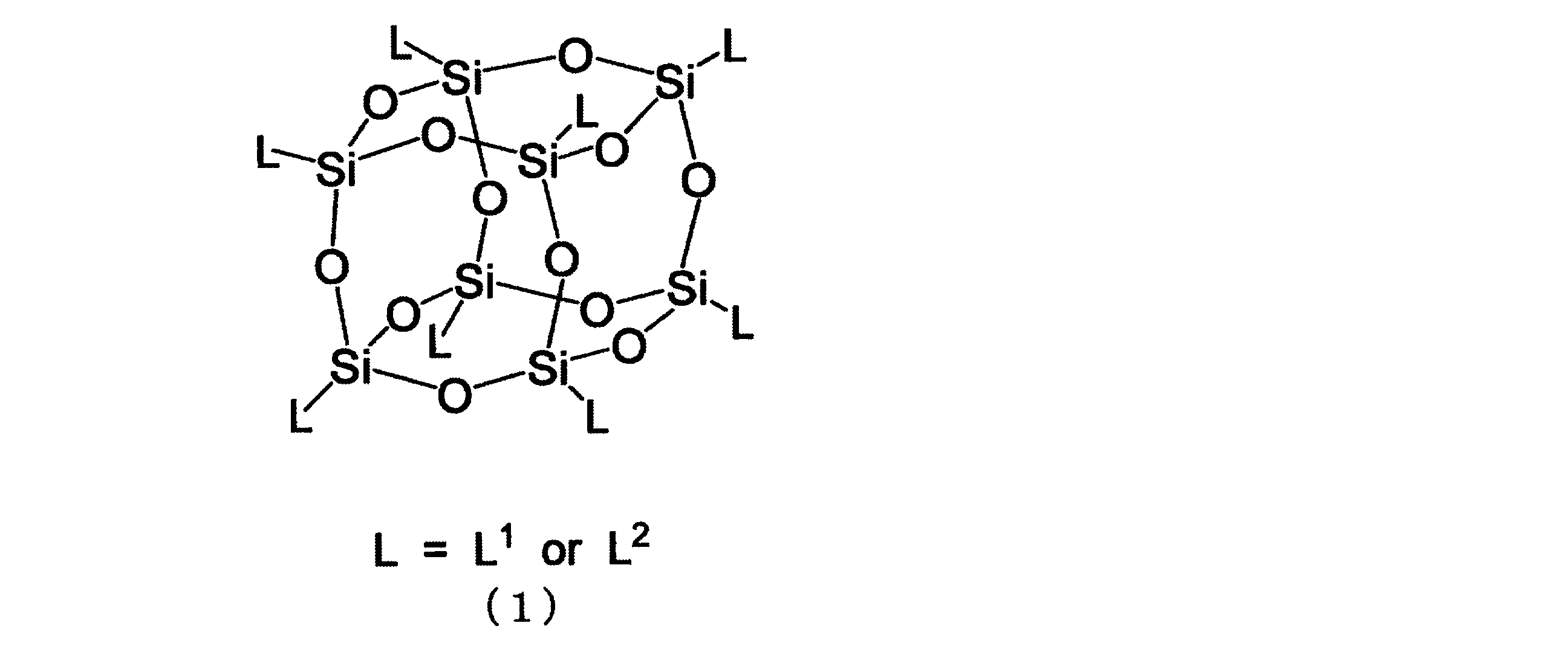

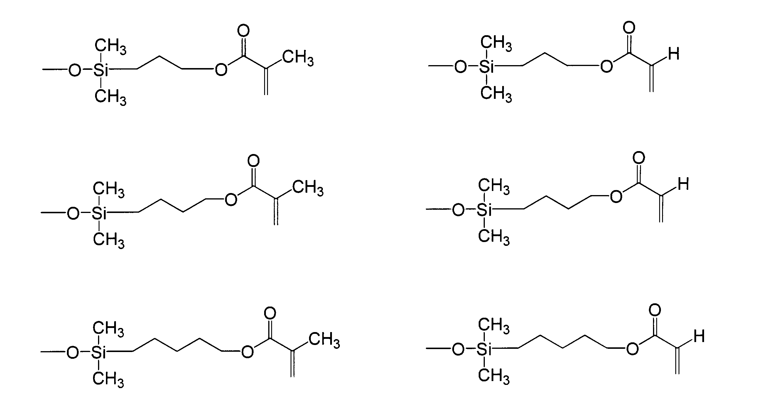

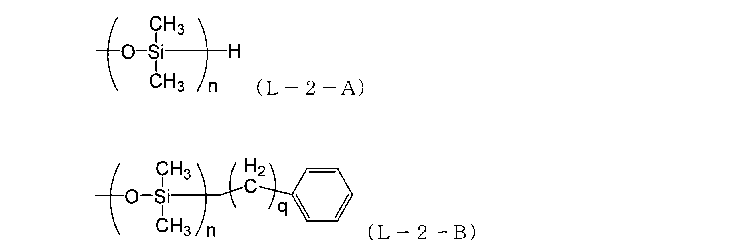
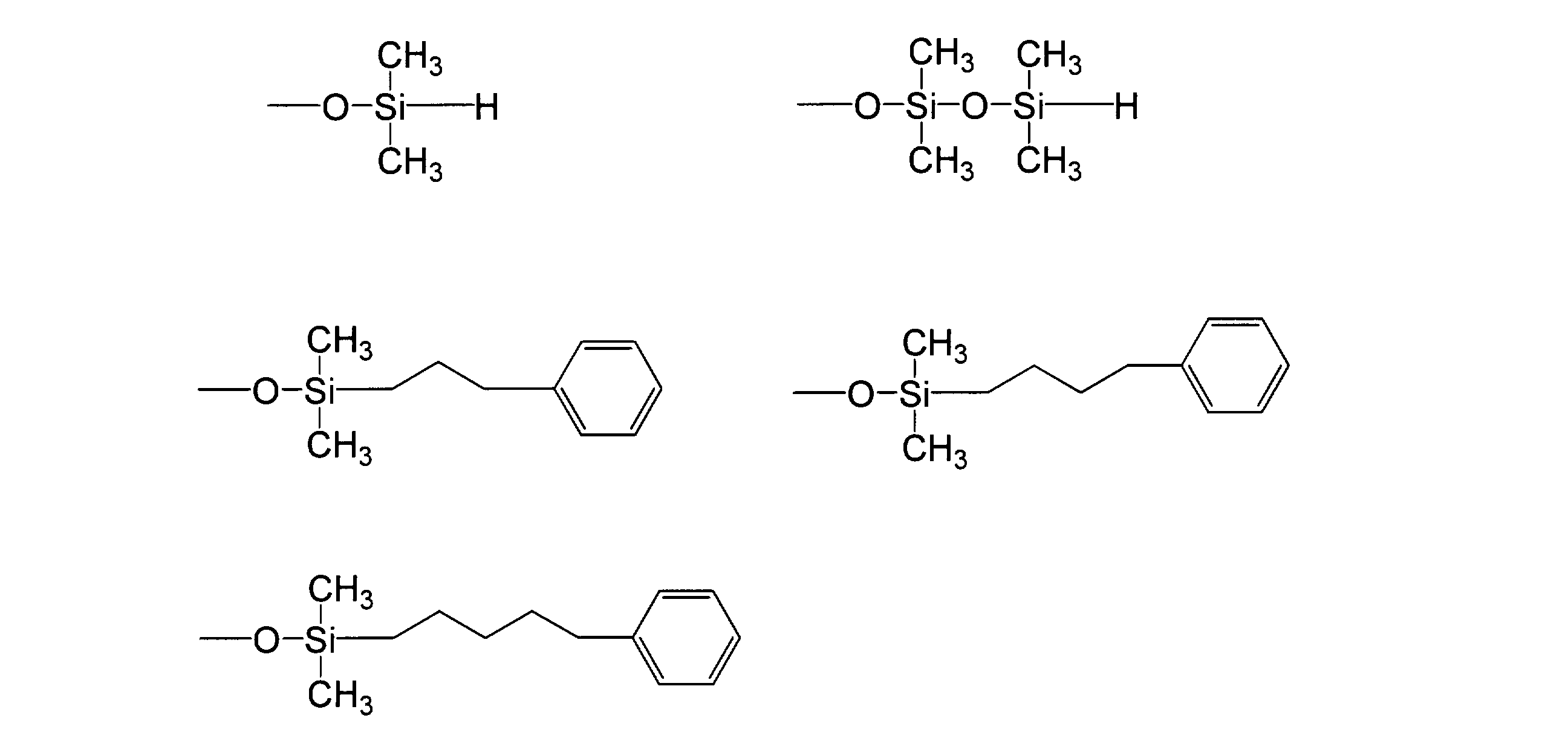
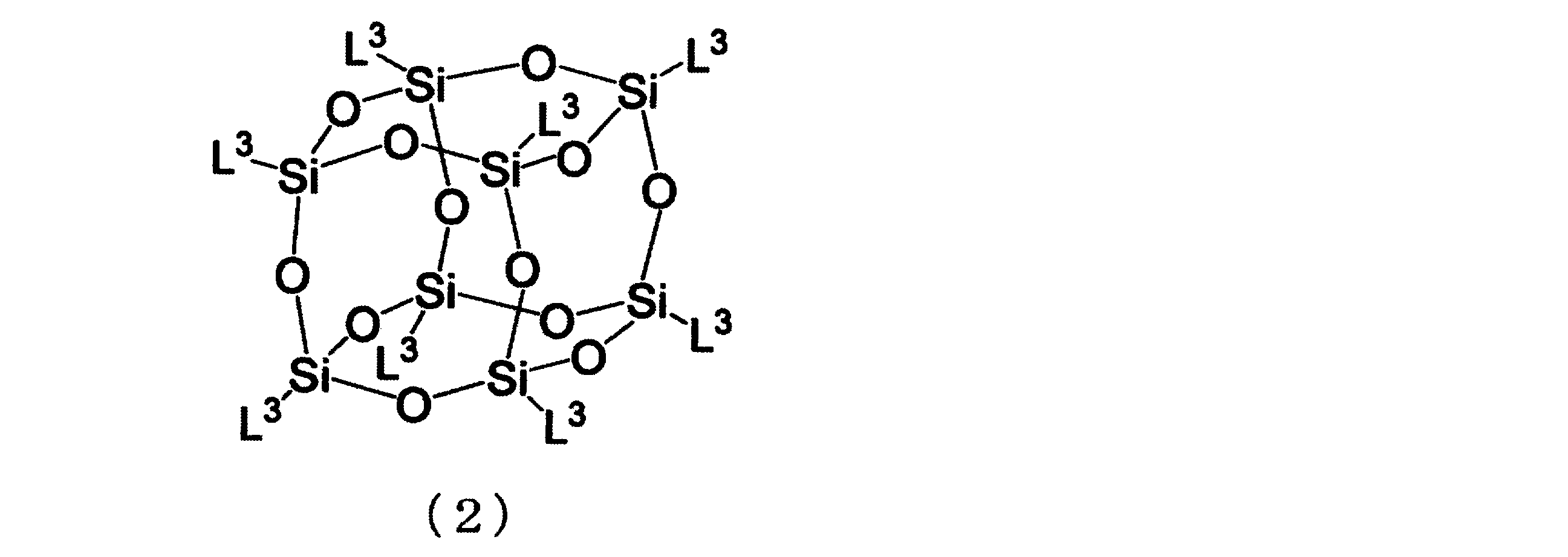

3-(トリメトキシシリル)プロピルメタクリレート、3-(トリエトキシシリル)プロピルメタクリレート、3-(トリメトキシシリル)プロピルアクリレート、3-(トリエトキシシリル)プロピルアクリレート、メタクリロキシメチルトリエトキシシラン、メタクリロキシメチルトリメトキシシランなどのトリアルコキシシラン化合物、(3-アクリロキシプロピル)メチルジメトキシシラン、(メタクリロキシメチル)メチルジエトキシシラン、(メタクリロキシメチル)メチルジメトキシシラン、メタクリロキシプロピルメチルジエトキシシラン、メタクリロキシプロピルメチルジメトキシシランなどのジアルコキシシラン化合物;
メタクリロキシプロピルジメチルエトキシシラン、メタクリロキシプロピルジメチルメトキシシランなどのモノアルコキシシラン化合物。

テトラメトキシシラン、テトラエトキシシランなどのテトラアルコキシシラン化合物、メチルトリメトキシシラン、フェニルトリメトキシシラン、フェニルトリエトキシシランなどのトリアルコキシシラン化合物;
ジメチルジメトキシシラン、メチルフェニルジメトキシシラン、ジメチルジエトキシシラン、ジフェニルジエトキシシラン、メチルフェニルジエトキシシランなどのジアルコキシシラン化合物、トリメチルメトキシシランなどのモノアルコキシシラン化合物。
光重合開始剤としては、400nm以上の波長領域の光を吸収する光重合開始剤を使用することができる。この光重合開始剤は、波長400nm以上の光照射によってラジカルを発生し、このラジカルが作用して、シリコーン化合物(A)の重合が開始する。この重合により、シリコーン化合物(A)が高分子化・硬化して、本発明の第一の硬化性組成物の流動性が失われて硬化膜となる。この硬化膜からなる第一仮接着材層を少なくとも備える仮接着材を介して部材と基材とを仮接着させることができる。本発明の仮接着材が第一仮接着材層と第二仮接着材層を有する場合には、さらに、第一仮接着材層と第二仮接着材層の界面で、シリコーン化合物(A)と、第二仮接着材層に含まれる光重合性基および加水分解性基含有シリコーン化合物(B)(以下、「シリコーン化合物(B)」と称することがある。)の加水分解縮合物(以下、「加水分解縮合物(B)」と称することがある。)との重合が起きる。これにより、第一仮接着材層と第二仮接着材層を接着させることができる。また、第二仮接着材層に含まれる加水分解縮合物(B)についてもさらに高分子化・硬化することがある。これにより、第二仮接着材層と基材との接着強度を向上させることができる。
ベンゾフェノン、オルソベンゾイン安息香酸メチル、4-ベンゾイル-4’-メチルジフェニルサルファイド、カンファーキノン、2-ヒドロキシ-1-{4-[4-(2-ヒドロキシ-2-メチルプロピオニル)ベンジル]フェニル}-2-メチルプロパン-1-オン、1-ヒドロキシシクロヘキシルフェニルケトン、1-[4-(2-ヒドロキシエトキシ)-フェニル]-2-ヒドロキシ-2-メチル-1-プロパン-1-オン)、2-ベンジル-2-ジメチルアミノ-1-(4-モルフォリノフェニル)-ブタノン-1、2-(ジメチルアミノ)-2-[(4-メチルフェニル)メチル]-1-[4-(4-モルホリニル)フェニル]-1-ブタノン、オキシフェニル酢酸と2-[2-オキソ-2-フェニルアセトキシエトキシ]エチルエステルとオキシフェニル酢酸と2-(2-ヒドロキシエトキシ)エチルエステルの混合物、2-メチル-1-(4-メチルチオフェニル)-2-モルフォリノプロパン-1-オン、ビス(2,4,6-トリメチルベンゾイル)フェニルホスフィンオキサイド、ビス(η5-2,4-シクロペンタジエン-1-イル)-ビス(2,6-ジフルオロ-3-(1H-ピロ-ル-1-イル)-フェニル)チタニウム。
Irgacure127、Irgacure184、Irgacure2959、Irgacure369、Irgacure379、Irgacure379EG、Irgacure907、Irgacure1700、Irgacure1800、Irgacure1850、Irgacure1870、Irgacure819、Irgacure784、Irgacure4265、Irgacure754。
光酸発生剤としては、400nm以上の波長領域の光を吸収する光酸発生剤を使用することができる。この光酸発生剤は、波長400nm未満の光照射によって、酸を発生する。発生した酸は、後述するように、本発明の第一の硬化性組成物に含まれる金属化合物と反応し、ガスや水を発生させる。
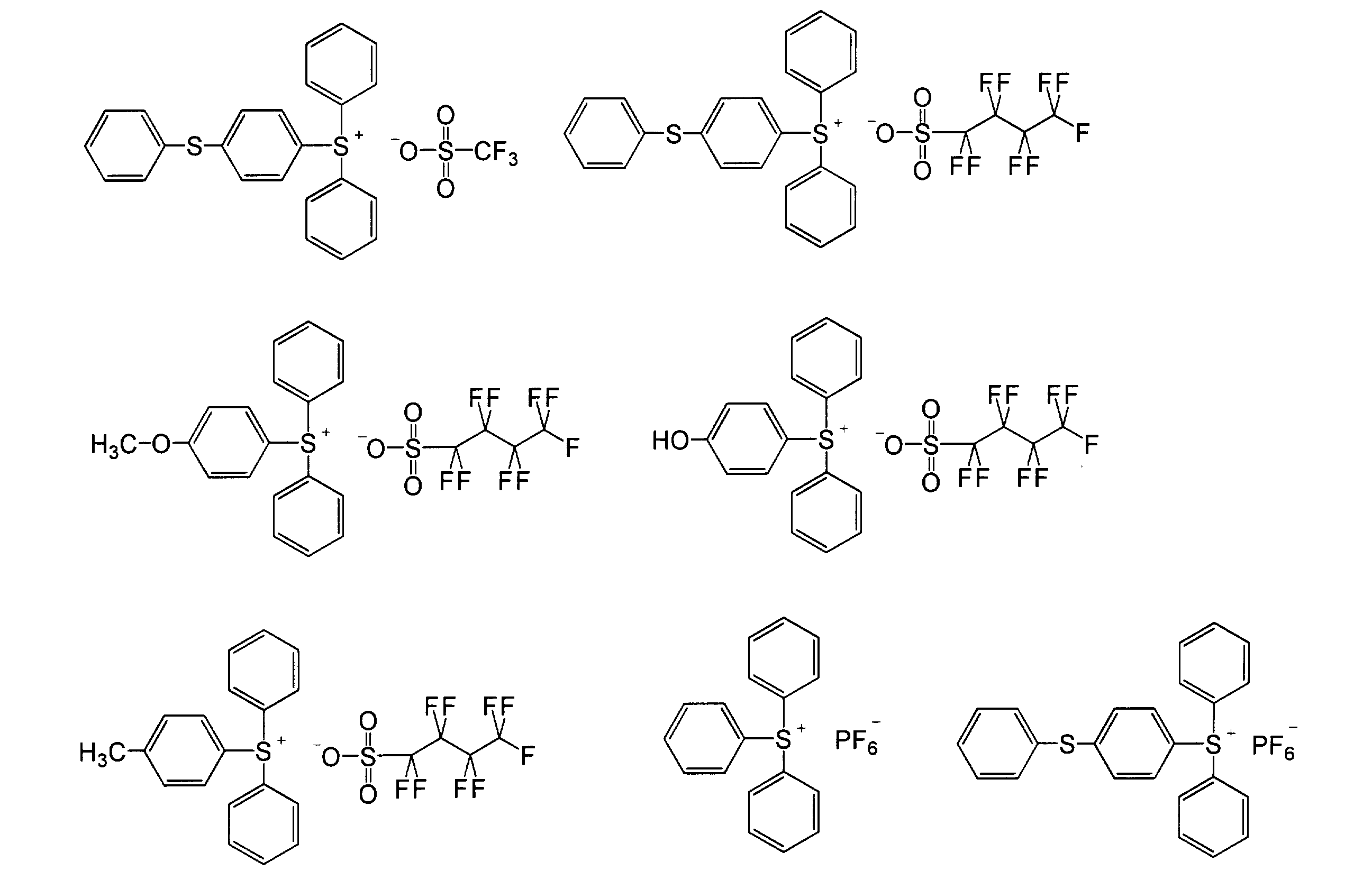
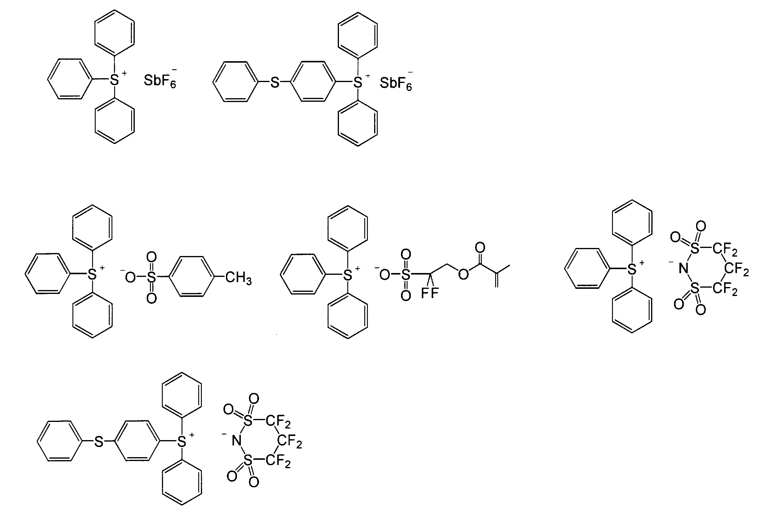
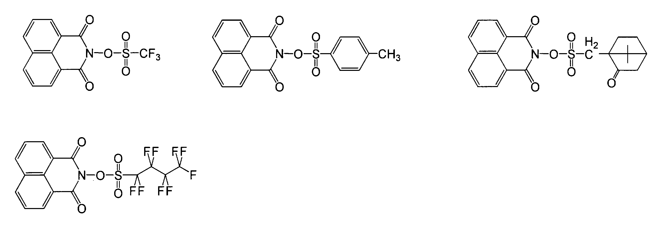
金属化合物としては、金属炭酸塩、金属酸化物および金属酸化物からなる群から選ばれる1種以上の金属化合物を使用することができる。このような金属化合物としては、以下に示す金属炭酸塩、金属酸化物、金属水酸化物が挙げられるが、これらに限定されるものではない。
金属炭酸塩:炭酸リチウム(Li2CO3、融点:723℃)、炭酸ナトリウム(Na2CO3、融点:851℃)、炭酸カリウム(K2CO3、融点:891℃)、炭酸ルビジウム(Rb2CO3、融点:837℃)、炭酸セシウム(Cs2CO3、融点:610℃)、炭酸カルシウム(Ca2CO3、融点:825℃)、炭酸バリウム(BaCO3、融点:811℃)、炭酸マグネシウム(MgCO3、融点:350℃)、炭酸ストロンチウム(SrCO3、融点:1497℃)、炭酸コバルト(CoCO3)。
金属酸化物:酸化リチウム(Li2O、融点:1570℃)、酸化ナトリウム(Na2O、融点:1132℃)、酸化カリウム(K2O、融点:350℃)、酸化ベリリウム(BeO、融点:2570℃)、酸化マグネシウム(MgO、融点:2800℃)、酸化カルシウム(CaO、融点:2613℃)、二酸化チタン(TiO2、融点:1870℃)、三酸化二クロム(Cr2O3、融点:2435℃)、二酸化マンガン(MnO2、融点:535℃)、三酸化二鉄(Fe2O3、融点:1566℃)、四酸化三鉄(Fe3O4、融点:1597℃)、酸化コバルト(CoO、融点:1933℃)、酸化ニッケル(NiO、融点:1984℃)、酸化銅(CuO、融点:1201℃)、酸化銀(Ag2O、融点:280℃)、酸化亜鉛(ZnO、融点:1975℃)、酸化アルミニウム(Al2O3、融点:2072℃)、酸化スズ(SnO、融点:1080℃)、酸化イッテルビウム(Yb2O3、融点:2346℃)。
金属水酸化物:水酸化リチウム(LiOH、融点:462℃)、水酸化ナトリウム(NaOH、融点:318℃)、水酸化カリウム(KOH、融点:360℃)、水酸化マグネシウム(Mg(OH)2、融点:350℃)、水酸化カルシウム(Ca(OH)2、融点:580℃)、水酸化ストロンチウム(Sr(OH)2、融点:375℃)、水酸化バリウム(Ba(OH)2、融点:408℃)、水酸化鉄(Fe(OH)2、融点:350~400℃)。

第一の硬化性組成物は、本発明の仮接着材と部材との接着力の向上や調整を目的として、極性基を有する化合物を添加物として含んでいても良い。極性基としては、特に限定されないが、ヒドロキシル基、カルボン酸基、シラノール基、リン酸基などが挙げられる。このような化合物としては、1つ以上の極性基を有し、かつ、1つ以上の光重合性基を有する化合物が好ましく、具体的には、メタクリル酸(2-ヒドロキシエチル)(略称:HEMA、和光純薬製)、ペンタエリスリトールトリアクリレート(大阪有機化学工業株式会社製、商品名:ビスコート#300)、エポキシアクリレート(大阪有機化学工業株式会社製、商品名:ビスコート#540)、トリ(2-アクリロイルオキシエチル)ホスフェート(大阪有機化学工業株式会社製、商品名:ビスコート3PA)、またはビス(2-メタクリロイルオキシエチル)リン酸エステル(日本化薬株式会社製、商品名:KAYAMER PM-2)などが挙げられる。中でも、HEMAが特に好適に用いられる。
第一の硬化性組成物は、混合や混練を行うことが好ましい。これにより、第一の硬化性組成物における金属化合物や光酸発生剤の分散状態を良好にし、仮接着や剥離の再現性を高めることができる。混練は、具体的には、撹拌脱泡装置、乳鉢、ホモジナイザー、ロールミル、ニーダーなどの装置を用いて行う。
本発明の仮接着材は、第一の硬化性組成物の硬化膜からなる第一仮接着材層を少なくとも備える。
さらに、本発明の仮接着材は、光重合性基および加水分解性基含有シリコーン化合物(B)(以下、「シリコーン化合物(B)」と称することがある。)の加水分解縮合物を少なくとも含む第二の硬化性組成物の膜からなる第二仮接着材層を備えていてもよい。
シリコーン化合物(B)の光重合性基とは、光の照射により光重合性基含有シリコーン化合物(A)同士またはその他の光重合性基を有する化合物と重合することが可能である官能基を意味する。このような光重合性基としては、アクリロイル基、メタクリロイル基などが挙げられるがこれらに限定されない。また、シリコーン化合物(B)の加水分解性基は、例えば、アルコキシ基、塩素原子などが挙げられる。


第二の硬化性組成物は、光重合開始剤を含んでいてもよい。光重合開始剤を含むことで、仮接着時の波長400nm以上の光照射によって、第一の硬化性組成物と第二仮接着材層の間で、より広範囲で化学結合の形成が効率的に行われ、強固な接着が期待できる。この光重合開始剤としては、第一の硬化性組成物に含まれる光重合開始剤として例示したものと同じ種類の光重合開始剤が使用できる。第二の硬化性組成物における光重合開始剤の含有量は加水分解縮合物(B)に対して0.01~5質量%以下であればよい。
第二の硬化性組成物は、公知の酸化防止剤、シリカなどのフィラーを含んでいてもよい。フィラーを含むことで、耐熱性をさらに高めることができる。
本発明の構造体は、本発明の仮接着材を介して部材と基材とを仮接着してなる。部材と基材とは、後述の部材と基材の仮接着方法に従って仮接着することができる。
用いる部材は特に制限はない。例えば、水晶部材、ガラス部材、プラスチック部材、半導体ウエハなどを用いることができる。そのため、本発明の仮接着方法は、水晶振動子、ガラスレンズ、プラスチックレンズ、光ディスク、半導体ウエハなどの加工における仮接着に適用可能である。
用いる基材の材質は特に制限はない。後述するように、仮接着時における仮接着面への波長400nm以上の光照射や、剥離時における仮接着面への波長400nm未満の光照射の効率性の観点から、基材はこれらの照射光を透過できる材質のものが好ましい。このような材質の基材を用いることで、基材の非仮接着面から照射光を照射しても、該基材を介して仮接着面に照射光を届けることができる。このような基材の材質としては、例えば、水晶基材、ガラス基材、プラスチック基材が挙げられるがこれらに限定されず、用いる光源に応じて材質を適宜選択すればよい。
本発明の部材と基材の仮接着方法(以下、単に「本発明の仮接着方法」と称することがある。)は、以下の第1工程~第4工程を少なくとも含む。
第1工程: 第一の硬化性組成物の層を少なくとも含む硬化処理前の仮接着材を介して部材と基材とを積層する工程。
第2工程: 硬化処理前の仮接着材に波長400nm以上の光を照射して、硬化させて、部材と基材とを仮接着してなる構造体を得る工程。
第3工程: 構造体の部材を加工する工程。
第4工程: 加工後の構造体における硬化処理後の仮接着材に波長400nm未満の光を照射して、該構造体から部材を剥離する工程。
第6工程: 剥離後の基材に残存する硬化処理後の仮接着材の残渣を除去する工程。
第7工程: 第6工程で得られた基材を第1工程に再利用する工程。
第5工程: 剥離した部材に残存する硬化処理後の仮接着材の残渣を除去する工程。
第1工程では、本発明の第一の硬化性組成物の層を少なくとも含む硬化処理前の仮接着材を介して部材と基材とを積層する。この硬化処理前の仮接着材は、第二仮接着材層をさらに備えていてもよく、この場合には、第一の硬化性組成物の層は、部材と第二仮接着材層とに接し、第二仮接着材層は第一の硬化性組成物の層と基材とに接するように積層される。すなわち、部材、第一の硬化性組成物の層、第二仮接着材層および基材はこの順序の積層となる。
第2工程では、硬化処理前の仮接着材に波長400nm以上の光を照射して、硬化させて、部材と基材とを仮接着してなる構造体を得る。
第3工程では、第2工程で得た構造体における部材を加工する工程である。この工程で施される加工には特に制限はなく、用いる部材、用途に応じて所望の加工を施すことができる。例えば、ガラス、光学レンズや光学部品、光学デバイス、プリズム、半導体実装部品等の加工においては、切断、研磨、研削、表面保護、孔開け等の所望の機械加工が施される。例えば、半導体ウエハの加工を例示すると、半導体ウエハを研削または研磨して、該ウエハの厚みを薄くしていく薄型ウエハの製造加工であったり、電極形成加工、金属配線形成加工、保護膜形成加工等がこの加工に含まれる。より具体的には、電極等の形成のための金属スパッタリング、金属スパッタリング層をエッチングするウェットエッチング、金属配線形成のマスクとするためのレジストの塗布、露光、及び現像によるパターンの形成、レジストの剥離、ドライエッチング、金属めっきの形成、TSV形成のためのシリコンエッチング、シリコン表面の酸化膜形成など、公知のプロセスも挙げられる。
第4工程では、加工後の構造体における硬化処理後の仮接着材に波長400nm未満の光を照射して、該構造体から加工後の部材を剥離する。この剥離には、硬化処理後の仮接着材に、波長400nm未満の光を所定温度下、所定時間照射する方法を用いる。この光照射によって、第一仮接着材層に含まれる光酸発生剤から酸が発生し、この酸と、第一仮接着材層に含まれる金属化合物とが反応することでガスや水が生成する。このガスや水の生成による内部応力によって、構造体から加工後の部材を容易に剥離することができる。これにより、加工後の部材と基材とを分離することができる。この光照射処理の後に加工後の部材を構造体から剥離する方法は、特に制限はない。例えば、水平方法に沿って加工後の部材と基材を反対方向にスライドさせることにより両者を分離する方法、構造体の部材または基材の一方を水平に固定しておく、他方を水平方向から一定の角度を付けて持ち上げる方法などが挙げられる。
本発明の仮接着方法を採用すれば、硬化処理後の仮接着材の残渣は加工後の部材側にはほとんどまたは全く残らず、ほぼすべてまたは完全に基材側へ付着する。加工後の部材側に硬化処理後の仮接着材の残渣が少量残った場合にこれを除去する方法を説明する。硬化処理後の仮接着材の残渣の除去は、例えば、部材を洗浄することで行うことができる。加工後の部材の洗浄には、硬化処理後の仮接着材の残渣を溶解し、加工後の部材(加工物)に悪影響を与えない洗浄液であればすべて使用可能である。例えば、半導体ウエハの加工においては、具体的には、以下に挙げる有機溶剤が使用可能である:
イソプロパノール、PGMEA、PGME、MEK、ヘキサン、トルエン、N-メチルピロリドン、アセトン等。
これらの有機溶剤は、1種単独でも2種以上を組み合わせて用いてもよい。また、これらの有機溶剤に塩基類、酸類を添加した混合溶液としてもよい。これらの塩基類、酸類は水溶液であってもよい。また、これらの有機溶剤に既存の界面活性剤を添加することもできる。
第4工程により、硬化処理後の仮接着材の残渣はほぼすべてまたは完全に基材側へ付着する。第6工程では、これらの硬化処理後の仮接着材の残渣を基材から除去する。これらの硬化処理後の仮接着材の残渣の除去は、例えば、基材を洗浄することで行うことができる。洗浄方法は、硬化処理後の仮接着材の残渣を基材から除去できれば特に限定されないが、残渣除去後の基材を第1工程で再利用する場合には、該基材に悪影響を与えない方法を採用することが好ましい。例えば、基材としてガラスを用いる場合、第5工程に記載の洗浄方法、後述する塩基洗浄法、酸洗浄法などを採用することができ、塩基洗浄法、酸洗浄法を採用することが好ましい。
前記塩基洗浄法では、アルキル基の炭素数が1~4のテトラアルキルアンモニウムヒドロキシド、炭素数1~5のアルコールおよびN-メチルピロリドンからなる混合洗浄液で基材を洗浄する。この混合洗浄液の組成比は具体的には、前記テトラアルキルアンモニウムヒドロキシドと前記アルコールと前記N-メチルピロリドンの組成比が1~20:20~98:1~79の範囲であるものが好ましい。洗浄方法としては、例えば、この混合洗浄液を収容した浸漬槽に基材を浸漬する浸漬式洗浄、混合洗浄液をシャワー、スプレー、および/またはジェット等でかけ流すシャワリング法、スポンジやブラシ等を使用するスクラブ洗浄法、浸漬式洗浄に超音波を印加して洗浄効率を上げる超音波洗浄法、バブリング洗浄法等が挙げられる。基材と接触させる際の該混合洗浄液の温度は、20~120℃が好ましく、より好ましくは40~100℃である。
前記酸洗浄法は、基材を、硫酸と過酸化水素を含む洗浄液で洗浄(SPM洗浄)、または塩酸と過酸化水素と超純水の混合洗浄液で洗浄(HPM洗浄)し、その後、硝酸水溶液を用いて洗浄(硝酸洗浄)し、最後に水洗した後、乾燥する方法である。
第6工程を経た基材は、第1工程の基材として再利用することができる。
本発明のウエハ加工用仮接着材は、表面に回路形成面を有し、加工すべき裏面を有するウエハを支持体に仮接着するために、該ウエハの表面と該支持体の間に介在させるウエハ加工用仮接着材である。具体的には、前述の本発明の仮接着材をこのウエハ加工用仮接着材として用いる。ここで、ウエハとしては、前述の部材の材質として例示した半導体ウエハと同様の種類のものを用いることができ、支持体としては、前述の基材の材質として例示したガラス基材と同様の種類のものを用いることができる。
本発明のウエハと支持体の仮接着方法は、表面に回路形成面を有し、加工すべき裏面を有するウエハと支持体の仮接着方法であり、以下の工程(a)~(d)の工程を少なくとも含む。
工程(a): 第一の硬化性組成物の層を少なくとも含む硬化処理前のウエハ加工用仮接着材を介して、ウエハの表面と支持体とを積層する工程。
工程(b): 硬化処理前のウエハ加工用仮接着材層に波長400nm以上の光を照射して、硬化させて、ウエハの表面と支持体とを仮接着してなるウエハ加工用構造体を得る工程。
工程(c): ウエハ加工用構造体のウエハの裏面を加工する工程。
工程(d): 加工後のウエハ加工用構造体における硬化処理後のウエハ加工用仮接着材に波長400nm未満の光を照射して、該ウエハ加工用構造体からウエハを剥離する工程。
工程(f): 剥離後の支持体に残存する硬化処理後のウエハ加工用仮接着材の残渣を除去する工程、
工程(g): 工程(f)で得られた支持体を工程(a)に再利用する工程。
工程(e): 剥離したウエハの表面に残存する硬化処理後のウエハ加工用仮接着材の残渣を除去する工程。
工程(a)では、表面に回路形成面を有し、加工すべき裏面を有するウエハの表面と接し、かつ支持体と接する、本発明の第一の硬化性組成物の層を少なくとも含む硬化処理前のウエハ加工用仮接着材を介して該ウエハと該支持体とを積層する。この硬化処理前のウエハ加工用仮接着材は、第二仮接着材層をさらに備えていてもよく、この場合には、第一の硬化性組成物の層は、前記ウエハの表面と第二仮接着材層とに接し、第二仮接着材層は第一の硬化性組成物の層と支持体とに接するように積層される。すなわち、前記ウエハ、第一の硬化性組成物の層、第二仮接着材層および支持体はこの順序の積層となる。
工程(b)では、硬化処理前のウエハ加工用仮接着材に波長400nm以上の光を照射して、硬化させて、前記ウエハの表面と支持体とを仮接着してなるウエハ加工用構造体を得る。
工程(c)では、工程(b)で得たウエハ加工用構造体におけるウエハの裏面を加工する工程である。この工程で施される加工には特に制限はなく、所望の加工を施すことができる。例えば、ウエハの裏面を研削または研磨して、該ウエハの厚みを薄くしていく薄型ウエハの製造加工であったり、電極形成加工、金属配線形成加工、保護膜形成加工等がこの加工に含まれる。より具体的には、電極等の形成のための金属スパッタリング、金属スパッタリング層をエッチングするウェットエッチング、金属配線形成のマスクとするためのレジストの塗布、露光、及び現像によるパターンの形成、レジストの剥離、ドライエッチング、金属めっきの形成、TSV形成のためのシリコンエッチング、シリコン表面の酸化膜形成など、公知のプロセスも挙げられる。
工程(d)では、加工後のウエハ加工用構造体における硬化処理後のウエハ加工用仮接着材に波長400nm未満の光を照射して、該ウエハ加工用構造体から加工後のウエハを剥離する。この剥離には、硬化処理後のウエハ加工用仮接着材に、波長400nm未満の光を所定温度下、所定時間照射する方法を用いる。この光照射によって、第一仮接着材層に含まれる光酸発生剤から酸が発生し、この酸と、第一仮接着材層に含まれる金属化合物とが反応することでガスや水が生成する。このガスや水の生成による内部応力によって、加工後のウエハ加工用構造体から加工後のウエハを容易に剥離することができる。これにより、加工後のウエハと支持体とを分離することができる。この光照射処理の後に加工後のウエハを加工後のウエハ加工用構造体から剥離する方法は、特に制限はない。例えば、水平方法に沿って加工後のウエハと支持体を反対方向にスライドさせることにより両者を分離する方法、加工後のウエハまたは支持体の一方を水平に固定しておく、他方を水平方向から一定の角度を付けて持ち上げる方法などが挙げられる。
本発明のウエハと支持体の仮接着方法を採用すれば、硬化処理後のウエハ加工用仮接着材の残渣は加工後のウエハ側にはほとんどまたは全く残らず、ほぼすべてまたは完全に支持体側へ付着する。加工後のウエハ側に硬化処理後のウエハ加工用仮接着材の残渣が少量残った場合にこれを除去する方法を説明する。硬化処理後のウエハ加工用仮接着材の残渣の除去は、例えば、加工後のウエハを洗浄することで行うことができる。
工程(d)により、硬化処理後のウエハ仮接着材の残渣はほぼすべてまたは完全に支持体側へ付着する。工程(f)では、これらの硬化処理後のウエハ加工用仮接着材の残渣を支持体から除去する。これらの硬化処理後のウエハ加工用仮接着材の残渣の除去は、例えば、支持体を洗浄することで行うことができる。
工程(f)を経た支持体は、工程(a)の支持体として再利用することができる。
[調製例1-1]
以下の反応式にしたがって、メタクリロイル基を有する籠型シルセスキオキサン化合物を合成した。

500mLフラスコ内にフェニルトリメトキシシラン(信越化学工業株式会社製、商品名:KBM-103)(30.01g)、ジメチルジメトキシシラン(信越化学工業株式会社製、商品名:KBM-22)(19.51g)、3-(トリメトキシシリル)プロピルメタクリレート(19.43g)、イソプロピルアルコール(80g)、水(65g)、水酸化ナトリウム(0.20g)を採取した後、オイルバスにて90℃まで昇温した状態で、撹拌速度200rpmにて18時間撹拌し反応させた。静置して室温(25℃)にした後、イソプロピルエーテル(100mL)、水(100mL)を加えて、分液ロートにて有機層を分取した。硫酸マグネシウムを用いて脱水した後、エバポレーターにて有機溶媒を留去して、メタクリロイル基を有するアルコキシシランの加水分解縮合物[樹脂(I-2)](34.48g)を無色透明の粘性液体として得た。
[調製例2-1]
調製例1-1で得た樹脂(I-1)(2.00g)に、光重合開始剤としてビス(2,4,6-トリメチルベンゾイル)-フェニルホスフィンオキサイド(チバ・スペシャリティ・ケミカルズ株式会社製、商品名:Irgacure819)(0.03g)、光酸発生剤としてCPI-110TF(商品名、サンアプロ社製、以下同じ)(0.39g)、金属化合物として平均粒子径が2μmの炭酸リチウム(0.88g)、添加物としてペンタエリスリトールトリアクリレート(大阪有機化学工業株式会社製、商品名:ビスコート#300、以下同じ)(0.48g)をそれぞれ加えて、3本ロールミルで混練して液体状の組成物1を得た。
なお、光酸発生剤として用いたCPI-110TFは以下の化学構造式で表される。

金属化合物として炭酸リチウム(0.88g)の代わりに、平均粒子径が10μmの炭酸カリウム(1.40g)を用いた以外は調製例2-1と同様の方法により、液体状の組成物2を得た。
添加物としてペンタエリスリトールトリアクリレート(0.48g)の代わりに、メタクリル酸(2-ヒドロキシエチル)(略称:HEMA、和光純薬製、以下同じ)(0.45g)を用いた以外は調製例2-1と同様の方法により、液体状の組成物3を得た。
光重合開始剤としてビス(2,4,6-トリメチルベンゾイル)-フェニルホスフィンオキサイド(0.03g)の代わりに、ビス(η5-2,4-シクロペンタジエン-1-イル)-ビス(2,6-ジフルオロ-3-(1H-ピロ-ル-1-イル)-フェニル)チタニウム(商品名:Irgacure784、チバ・スペシャリティ・ケミカルズ株式会社製)(0.03g)を用いた以外は調製例2-1と同様の方法により、液体状の組成物4を得た。
光酸発生剤としてCPI-110TF(0.39g)の代わりに、TPS-109(0.41g)を用いた以外は調製例2-1と同様の方法により、液体状の組成物5を得た。
金属化合物として炭酸リチウムの代わりに水酸化カルシウム(2.11g)を用いた以外は調製例2-1と同様の方法により、液体状の組成物6を得た。
金属化合物として炭酸リチウムの代わりに水酸化カルシウム(2.11g)を用い、添加物としてビスコート#300の代わりにHEMA(0.70g)を用いた以外は調製例2-1と同様の方法により、液体状の組成物7を得た。
金属化合物として炭酸リチウムの代わりに水酸化カルシウム(2.11g)を用い、光酸発生剤としてCPI-110TFの代わりにTPS-109(0.34g)を用いた以外は調製例2-1と同様の方法により、液体状の組成物8を得た。
金属化合物として炭酸リチウムの代わりに水酸化リチウム(1.28g)を用いた以外は調製例2-1と同様の方法により、液体状の組成物9を得た。
化合物(A)として樹脂(I-1)の代わりに樹脂(I-2)を用い、金属化合物として炭酸リチウムの代わりに水酸化カルシウム(2.11g)を用いた以外は調製例2-1と同様の方法により、液体状の組成物10を得た。
化合物(A)として樹脂(I-1)の代わりに樹脂(I-2)を用い、金属化合物として炭酸リチウムの代わりに水酸化リチウム(1.28g)を用いた以外は調製例2-1と同様の方法により、液体状の組成物11を得た。
添加物としてビスコート#300を用いない以外は、調製例2-1と同様の方法により、液体状の組成物12を得た。
光酸発生剤としてCPI-110TFの代わりにTPS-109(0.34g)を用い、添加物としてビスコート#300を用いない以外は、調製例2-1と同様の方法により、液体状の組成物13を得た。
[調製例3-1]
ジムロートと撹拌翼を具備した2Lフラスコ内にフェニルトリメトキシシラン(信越化学工業株式会社製、商品名:KBM-103)(140.40g)、ジメチルジエトキシシラン(信越化学工業株式会社製、商品名:KBE-22)(131.14g)、3-(トリメトキシシリル)プロピルメタクリレート(東京化成株式会社製)(48.56g)、イソプロピルアルコール(213.32g)、水(160.96g)、酢酸(0.10g)を採取した後、オイルバスにて90℃まで昇温した状態で、撹拌速度200rpmにて6時間撹拌し反応させた。静置して室温(25℃)にした後、イソプロピルエーテル(400mL)、水(400mL)を加えて、分液ロートにて有機層を分取した。硫酸マグネシウムを用いて脱水した後、エバポレーターにて有機溶媒を留去して、無色透明の粘性液体(170.68g)を得た。このようにしてメタクリロイル基を有するアルコキシシランの加水分解縮合物(以下、「加水分解縮合物1」と表すことがある。)を得た。
次いで、この加水分解縮合物1をPGMEAへ溶解させ、加水分解縮合物1の濃度が33質量%のPGMEA溶液(以下、「(B)溶液1」と表すことがある。)とした。
メチルトリメトキシシラン(88.91g)、ジメチルジエトキシシラン(112.56g)、3-(トリメトキシシリル)プロピルメタクリレート(70.11g)、イソプロピルアルコール(203.79g)、水(144.45g)、酢酸(0.10g)を用いた以外は調整例3-1に記載した方法を用いて、メタクリロイル基を有するアルコキシシランの加水分解縮合物(以下、「加水分解縮合物2」と表すことがある。)を得た。
次いで、この加水分解縮合物2をPGMEAへ溶解させ、加水分解縮合物2の濃度が33質量%のPGMEA溶液(以下、「(B)溶液2」と表すことがある。)とした。
直径100mm、厚み1.1mmの無アルカリガラス基板(コーニング株式会社製、品番:7059、以下同じ)の表面を酸化セリウムの微粒子(アルドリッチ株式会社製、以下同じ)で研磨した。ディスペンサーを用いて、直径100mmのシリコンウエハ上に調製例2-1で調製した組成物1を0.6g塗布した。
次いで、このシリコンウエハ上の塗布面を、無アルカリガラス基板と重ね合わせて積層体1を得た。その後に下記の評価試験(1)~(6)を行った。結果を表3に示す。
<ガラス基板への第二仮接着材層の形成>
直径100mm、厚み1.1mmの無アルカリガラス基板の表面を酸化セリウムの微粒子で研磨した。続いてスピンコーターを用いて、調製例3-1で調製した前記(B)溶液1を無アルカリガラス基板の表面に1000rpmで10秒間、スピンコートした。次いで、200℃のホットプレート上で約20分間加熱乾燥させて、無アルカリガラス基板の表面に第二仮接着材層として加水分解縮合物1の樹脂層(II-1)を形成した。触針式表面形状測定器(米国Veeco製、形式:Dektak8、以下同じ)を用いて、この樹脂層(II-1)の厚みを測定したところ、0.7μmであった。
ディスペンサーを用いて、直径100mmのシリコンウエハ上に調製例2-1で調製した組成物1を0.6g塗布した。
次いで、このシリコンウエハ上の組成物塗布層を、無アルカリガラス基板上の第二仮接着材層と重ね合わせて積層体2を得た。その後に下記の評価試験(1)~(6)を行った。結果を表3に示す。
組成物1の代わりに組成物2を用いた以外は実施例2と同様の方法により、積層体3を得た。その後に下記の評価試験(1)~(6)を行った。結果を表3に示す。
組成物1の代わりに組成物3を用いた以外は実施例2と同様の方法により、積層体4を得た。その後に下記の評価試験(1)~(6)を行った。結果を表3に示す。
組成物1の代わりに組成物4を用いた以外は実施例2と同様の方法により、積層体5を得た。その後に下記の評価試験(1)~(6)を行った。結果を表3に示す。
組成物1の代わりに組成物5を用いた以外は実施例2と同様の方法により、積層体6を得た。その後に下記の評価試験(1)~(6)を行った。結果を表3に示す。
<ガラス基板への第二仮接着材層の形成>
直径100mm、厚み1.1mmの無アルカリガラス基板の表面を酸化セリウムの微粒子で研磨した。続いてスピンコーターを用いて、調製例3-2で調製した前記(B)溶液2を無アルカリガラス基板の表面に1000rpmで10秒間、スピンコートした。次いで、200℃のホットプレート上で約20分間加熱乾燥させて、無アルカリガラス基板の表面に加水分解縮合物1の樹脂層(II-2)を形成した。触針式表面形状測定器を用いて、この樹脂層(II-2)の厚みを測定したところ、1.5μmであった。
ディスペンサーを用いて、直径100mmのシリコンウエハ上に調製例2-1で調製した組成物1を0.6g塗布した。
次いで、このシリコンウエハ上の組成物塗布層を、無アルカリガラス基板上の第二仮接着材層と重ね合わせて積層体7を得た。その後に下記の評価試験(1)~(6)を行った。結果を表3に示す。
無アルカリガラス基板の代わりにホウケイ酸ガラスを用いた以外は実施例2と同様の方法により、積層体8を得た。その後に下記の評価試験(1)~(6)を行った。結果を表3に示す。
無アルカリガラス基板の代わりにソーダライムガラスを用いた以外は実施例2と同様の方法により、積層体9を得た。その後に下記の評価試験(1)~(6)を行った。結果を表3に示す。
直径100mm、厚み1.1mmの無アルカリガラス基板の表面を酸化セリウムの微粒子で研磨しなかった以外は、実施例1と同様の方法で積層体10を得た。その後に下記の評価試験(1)~(6)を行った。結果を表3に示す。
組成物1の代わりに組成物6を用いた以外は実施例1と同様の方法により、積層体11を得た。その後に下記の評価試験(1)~(6)を行った。結果を表3に示す。
組成物1の代わりに組成物6を用いた以外は実施例2と同様の方法により、積層体12を得た。その後に下記の評価試験(1)~(6)を行った。結果を表3に示す。
組成物1の代わりに組成物7を用いた以外は実施例2と同様の方法により、積層体13を得た。その後に下記の評価試験(1)~(6)を行った。結果を表3に示す。
組成物1の代わりに組成物8を用いた以外は実施例2と同様の方法により、積層体13を得た。その後に下記の評価試験(1)~(6)を行った。結果を表3に示す。
組成物1の代わりに組成物6を用い、(B)溶液1を用いて樹脂層(II-1)を第二仮接着材層として形成する代わりに(B)溶液2を用いて樹脂層(II-2)を形成した以外は実施例2と同様の方法により、積層体15を得た。その後に下記の評価試験(1)~(6)を行った。結果を表3に示す。
組成物1の代わりに組成物9を用いた以外は実施例2と同様の方法により、積層体16を得た。その後に下記の評価試験(1)~(6)を行った。結果を表3に示す。
組成物1の代わりに組成物10を用いた以外は実施例2と同様の方法により、積層体17を得た。その後に下記の評価試験(1)~(6)を行った。結果を表3に示す。
組成物1の代わりに組成物11を用いた以外は実施例2と同様の方法により、積層体18を得た。その後に下記の評価試験(1)~(6)を行った。結果を表3に示す。
組成物1の代わりに組成物12を用いた以外は実施例2と同様の方法により、積層体19を得た。その後に下記の評価試験(1)~(6)を行った。結果を表3に示す。
組成物1の代わりに組成物13を用いた以外は実施例2と同様の方法により、積層体20を得た。その後に下記の評価試験(1)~(6)を行った。結果を表3に示す。
金属化合物として炭酸リチウムを用いない以外は調製例2-1と同様の方法により、液体状の比較用組成物1を得た。続いて、組成物1の代わりにこの比較用組成物1を用いた以外は実施例2と同様の方法により、比較用積層体1を得た。その後に下記の評価試験(1)~(6)を行った。結果を表3に示す。
光酸発生剤としてCPI-110TFを用いない以外は調製例2-1と同様の方法により、液体状の比較用組成物2を得た。続いて、組成物1の代わりにこの比較用組成物2を用いた以外は実施例2と同様の方法により、比較用積層体2を得た。その後に下記の評価試験(1)~(6)を行った。結果を表3に示す。
光重合開始剤としてIrgacure819を用いない以外は調製例2-1と同様の方法により、液体状の比較用組成物3を得た。続いて、組成物1の代わりにこの比較用組成物3を用いた以外は実施例2と同様の方法により、比較用積層体3を得た。その後に下記の評価試験(1)~(6)を行った。結果を表3に示す。
樹脂(I-1)を用いず、添加物としてペンタエリスリトールトリアクリレート(0.48g)の代わりに、トリメチロールプロパントリアクリレート(略称:TMPTA)(1.92g)を用いた以外は調製例2-1と同様の方法により、液体状の比較用組成物4を得た。続いて、組成物1の代わりにこの比較用組成物4を用いた以外は実施例2と同様の方法により、比較用積層体4を得た。その後に以下の評価試験(1)~(6)を行った。結果を表3に示す。
実施例2と同様の方法により比較用積層体5を得た。その後に下記の評価試験(1)~(6)を行った。ただし、評価試験(1)においては、波長405nmのLED光照射ではなく、高圧水銀灯による紫外線光を30秒間照射した。結果を表3に示す。
(1)接着性試験
実施例1~20および比較例1~4で得られた積層体1~20、比較用積層体1~4を、それぞれ波長405nmのLED光で30秒間照射した。比較例5で得られた比較用積層体5には、高圧水銀灯による紫外線光を30秒間照射した。その後、接着性試験として、支持体側を水平に固定して、シリコンウエハを持ち上げて、剥離しなかった場合を「○」と、剥離した場合を「×」と評価した。
グラインダー(DISCO製、DAG810)でダイヤモンド砥石を用いて、接合した後の積層体1~20ならびに比較用積層体1、2、4および5のシリコンウエハをそれぞれ裏面研削した。基板厚が50μmとなるまでグラインドした後、光学顕微鏡(100倍)にてクラック、剥離などの異常の有無を調べた。異常が発生せず、かつ目視でシリコンウエハの研磨面に干渉縞が確認されなかった場合を非常に良好と評価して「◎」で示し、異常が発生しなかった場合を良好と評価して「○」で示し、異常が発生した場合を不良と評価して「×」と示し、裏面研削耐性試験を実施しなかった場合を「-」と示した。なお、比較例3では、前述の接着性試験で剥離してしまったことから、裏面研削耐性試験は実施しなかった。
シリコンウエハを裏面研削した後の積層体1~20ならびに比較用積層体1、2および4について、窒素雰囲気下でホットプレートを用いて280℃で10分間加熱した後の外観異常の有無を調べた。外観異常が発生しなかった場合を非常に良好と評価して「◎」で示し、外観異常がほとんど発生しなかった場合を良好と評価して「○」で示し、外観異常が明らかに発生した場合を不良と評価して「×」で示し、耐熱性試験を実施しなかった場合を「-」で示した。なお、比較例3では、前述の(2)の試験と同様に耐熱性試験は中止した。比較例5についても、前述の裏面研削耐性試験でクラックなどの異常が発生したことから耐熱性試験は実施しなかった。
シリコンウエハを裏面研削した後の積層体1~20ならびに比較用積層体1および2に対して、それぞれ、支持体から見て接着面の裏側から該積層体(該比較用積層体)に向けて、高圧水銀灯による紫外線を室温で300秒間照射した。その後、室温にて、支持体をピンセットにて持ち上げることで、支持体を剥離した。支持体およびシリコンウエハを割ることなく剥離できた場合を「○」で示し、割れなどの異常が発生した場合を「×」と示し、剥離性試験を実施しなかった場合を「-」で示した。なお、比較例3および5では、前述の(2)、(3)の試験と同様に剥離性試験は実施しなかった。比較例4では、前述の耐熱性試験で外観異常が発生してしまったことから剥離性試験は実施しなかった。
上記剥離性試験の後に、シリコンウエハと支持体を目視にて観察して、シリコンウエハ上の接着残渣が支持体側の接着残渣の5%未満であった場合を「◎」と示し、10%未満であった場合を「○」と、50%未満であった場合を「△」と示し、50%以上であった場合を「×」と示し、シリコンウエハ上残渣評価を実施しなかった場合を「-」で示した。なお、比較例3~5では、前述の(2)~(4)の試験と同様にシリコンウエハ上残渣評価は実施しなかった。比較例1および2においても、前述の剥離性試験で支持体またはウエハに割れなどの異常が発生したことからシリコンウエハ上残渣評価は実施しなかった。
上記剥離性試験の後に、接着残渣が付着したシリコンウエハと支持体に対して、質量比で25%テトラメチルアンモニウムハイドロキサイド水溶液:イソプロパノール:N-メチルピロリドン=50:25:25の混合洗浄液による洗浄を行った。150℃で乾燥した後、シリコンウエハと支持体の表面について、光学顕微鏡(100倍)にて接着残渣の付着、基板の損傷などの異常の有無を調べた。3分以内の洗浄で接着残渣が除去でき、かつ基板表面に損傷などの異常が発生しなかった場合を非常に良好と評価して「◎」で示し、15分以内の洗浄で接着残渣が除去でき、かつ基板表面に損傷などの異常が発生しなかった場合を良好と評価して「○」で示し、基板表面に接着残渣の付着および/または損傷などの異常が発生した場合を不良と評価して「×」と示し、洗浄除去性試験を実施しなかった場合を「-」と示した。なお、実施例2~9および12~20においては、前述の(5)の試験で非常に良好な結果であったため、洗浄除去性試験は敢えて実施しなかった。比較例1~5については、前述の(2)~(5)の試験と同様に洗浄除去性試験は実施しなかった。


2: 基材
3: 仮接着材
3a’: 第一の硬化性組成物の層
3a: 第一仮接着材層
3b: 第二仮接着材層
10: 構造体
20: 積層体
Claims (16)
- 光重合性基含有シリコーン化合物(A)と、400nm以上の波長領域の光を吸収する光重合開始剤と、400nm未満の波長領域の光を吸収する光酸発生剤と、金属炭酸塩、金属水酸化物および金属酸化物からなる群から選ばれる1種以上の金属化合物とを少なくとも含み、流動性を有する、第一の硬化性組成物。
- 光重合性基含有シリコーン化合物(A)が、アクリロイル基もしくはメタクリロイル基を有する籠型シルセスキオキサン化合物、または、一般式(3)で表されるアルコキシシラン化合物を少なくとも含む組成物を加水分解縮合して得られる加水分解縮合物である、請求項1に記載の第一の硬化性組成物。

- 請求項1または2に記載の第一の硬化性組成物の硬化膜からなる第一仮接着材層を少なくとも備える、仮接着材。
- さらに、光重合性基および加水分解性基含有シリコーン化合物(B)の加水分解縮合物を少なくとも含む第二の硬化性組成物の膜からなる第二仮接着材層を備える、請求項3に記載の仮接着材。
- 光重合性基および加水分解性基含有シリコーン化合物(B)の加水分解縮合物が、一般式(5)で表されるアルコキシシラン化合物を少なくとも含む組成物を加水分解縮合して得られる加水分解縮合物である、請求項4に記載の仮接着材。

- 第二の硬化性組成物が、光重合開始剤をさらに含む、請求項4または5に記載の仮接着材。
- 請求項3乃至6の何れか一に記載の仮接着材を介して部材と基材とを仮接着してなる、構造体。
- 以下の第1乃至第4工程を含む、部材と基材の仮接着方法。
第1工程: 請求項1または2に記載の第一の硬化性組成物の層を少なくとも含む硬化処理前の仮接着材を介して部材と基材とを積層する工程、
第2工程: 硬化処理前の仮接着材層に波長400nm以上の光を照射して、硬化させて、部材と基材とを仮接着してなる構造体を得る工程、
第3工程: 構造体の部材を加工する工程、
第4工程: 加工後の構造体における硬化処理後の仮接着材に波長400nm未満の光を照射して、該構造体から部材を剥離する工程。 - 硬化処理前の仮接着材層が、基材と第一の硬化性組成物の層とに接する第二仮接着材層を備え、該第二仮接着材層は、光重合性基および加水分解性基含有シリコーン化合物(B)の加水分解縮合物を少なくとも含む第二の硬化性組成物の膜である、請求項8に記載の方法。
- 光重合性基および加水分解性基含有シリコーン化合物(B)の加水分解縮合物が、一般式(5)で表されるアルコキシシラン化合物を少なくとも含む組成物を加水分解縮合して得られる加水分解縮合物を少なくとも含む、請求項9に記載の方法。

- 剥離した基材から硬化処理後の仮接着材の残渣を除去し、除去後の基材を再利用する、請求項8乃至10の何れか一に記載の方法。
- 表面に回路形成面を有し、加工すべき裏面を有するウエハを支持体に仮接着するために、前記ウエハの表面と前記支持体の間に介在させるウエハ加工用仮接着材であって、該ウエハ加工用仮接着材が、請求項3乃至6の何れか一に記載の仮接着材である、ウエハ加工用仮接着材。
- 表面に回路形成面を有し、加工すべき裏面を有するウエハの表面と支持体の仮接着方法であり、以下の工程(a)~(d)を少なくとも含む、ウエハと支持体の仮接着方法。
工程(a): 請求項1または2に記載の第一の硬化性組成物の層を少なくとも含む硬化処理前のウエハ加工用仮接着材を介して、ウエハの表面と支持体とを積層する工程、
工程(b): 硬化処理前のウエハ加工用仮接着材層に波長400nm以上の光を照射して、硬化させて、ウエハの表面と支持体とを仮接着してなるウエハ加工用構造体を得る工程、
工程(c): ウエハ加工用構造体のウエハの裏面を加工する工程、
工程(d): 加工後のウエハ加工用構造体における硬化処理後のウエハ加工用仮接着材に波長400nm未満の光を照射して、該ウエハ加工用構造体からウエハを剥離する工程。 - 硬化処理前のウエハ加工用仮接着材が、支持体と第一の硬化性組成物の層とに接する第二仮接着材層を備え、該第二仮接着材層は、光重合性基および加水分解性基含有シリコーン化合物(B)の加水分解縮合物を少なくとも含む第二の硬化性組成物の膜である、請求項13に記載の方法。
- 光重合性基および加水分解性基含有シリコーン化合物(B)の加水分解縮合物が、一般式(5)で表されるアルコキシシラン化合物を少なくとも含む組成物を加水分解縮合して得られる加水分解縮合物を少なくとも含む、請求項14に記載の方法。

- 剥離した支持体から硬化処理後のウエハ加工用仮接着材の残渣を除去し、除去後の支持体を再利用する、請求項13乃至15の何れか一に記載の方法。
Priority Applications (2)
| Application Number | Priority Date | Filing Date | Title |
|---|---|---|---|
| US15/122,646 US20170073547A1 (en) | 2014-04-24 | 2015-04-15 | Curable Composition, Temporary Bonding Material, and Method for Temporarily Bonding Component Part and Substrate By Same |
| KR1020167032384A KR20160148612A (ko) | 2014-04-24 | 2015-04-15 | 경화성 조성물, 가접착재 및 이들을 이용한 부재와 기재의 가접착 방법 |
Applications Claiming Priority (6)
| Application Number | Priority Date | Filing Date | Title |
|---|---|---|---|
| JP2014089772 | 2014-04-24 | ||
| JP2014089771 | 2014-04-24 | ||
| JP2014-089772 | 2014-04-24 | ||
| JP2014-089771 | 2014-04-24 | ||
| JP2015079959A JP2015214681A (ja) | 2014-04-24 | 2015-04-09 | 硬化性組成物、仮接着材およびこれらを用いた部材と基材の仮接着方法 |
| JP2015-079959 | 2015-04-09 |
Publications (1)
| Publication Number | Publication Date |
|---|---|
| WO2015163201A1 true WO2015163201A1 (ja) | 2015-10-29 |
Family
ID=54332368
Family Applications (1)
| Application Number | Title | Priority Date | Filing Date |
|---|---|---|---|
| PCT/JP2015/061531 Ceased WO2015163201A1 (ja) | 2014-04-24 | 2015-04-15 | 硬化性組成物、仮接着材およびこれらを用いた部材と基材の仮接着方法 |
Country Status (5)
| Country | Link |
|---|---|
| US (1) | US20170073547A1 (ja) |
| JP (1) | JP2015214681A (ja) |
| KR (1) | KR20160148612A (ja) |
| TW (1) | TWI566042B (ja) |
| WO (1) | WO2015163201A1 (ja) |
Cited By (2)
| Publication number | Priority date | Publication date | Assignee | Title |
|---|---|---|---|---|
| JP2018150513A (ja) * | 2017-03-09 | 2018-09-27 | 協立化学産業株式会社 | 硬化性樹脂組成物及び加工フィルムの製造方法 |
| CN109689699A (zh) * | 2016-08-24 | 2019-04-26 | 日立化成株式会社 | 固化性树脂组合物、图像显示装置及图像显示装置的制造方法 |
Families Citing this family (8)
| Publication number | Priority date | Publication date | Assignee | Title |
|---|---|---|---|---|
| JP6463664B2 (ja) * | 2015-11-27 | 2019-02-06 | 信越化学工業株式会社 | ウエハ加工体及びウエハ加工方法 |
| KR101819290B1 (ko) * | 2015-11-30 | 2018-01-17 | 주식회사 포스코 | 광택도 조절이 용이한 표면처리 금속재 및 그 제조방법 |
| CN106935696B (zh) | 2015-12-29 | 2019-06-07 | 通用电气照明解决方案有限公司 | 用于光过滤的复合材料、发光设备和用于确定复合材料的掺杂浓度或厚度的方法 |
| WO2018168475A1 (ja) * | 2017-03-17 | 2018-09-20 | 住友ベークライト株式会社 | 粘着テープセットおよび半導体素子移送用粘着テープ |
| JP7331351B2 (ja) * | 2018-11-29 | 2023-08-23 | 株式会社レゾナック | 半導体装置の製造方法及び仮固定材用積層フィルム |
| CN113396169A (zh) * | 2019-02-08 | 2021-09-14 | 日铁化学材料株式会社 | 光硬化性硅酮树脂组合物及由其硬化成的硅酮树脂成形体以及所述成形体的制造方法 |
| TWI846610B (zh) * | 2023-09-27 | 2024-06-21 | 臺灣永光化學工業股份有限公司 | 低溫固烤之感光性樹脂組成物及其用途 |
| CN119419187A (zh) * | 2024-11-05 | 2025-02-11 | 成都莱普科技股份有限公司 | 键合结构、芯片及键合结构的制备方法 |
Citations (5)
| Publication number | Priority date | Publication date | Assignee | Title |
|---|---|---|---|---|
| JP2008094877A (ja) * | 2006-10-06 | 2008-04-24 | Shin Etsu Chem Co Ltd | 紫外線硬化型熱伝導性シリコーン組成物 |
| JP2008298880A (ja) * | 2007-05-29 | 2008-12-11 | Nagase Chemtex Corp | 感光性組成物 |
| JP2011006620A (ja) * | 2009-06-29 | 2011-01-13 | Sanyo Chem Ind Ltd | ハードコート用組成物 |
| JP2012107194A (ja) * | 2010-10-26 | 2012-06-07 | Sekisui Chem Co Ltd | 粘着剤組成物及び半導体加工用粘着テープ |
| JP2014077063A (ja) * | 2012-10-10 | 2014-05-01 | Kaneka Corp | 活性エネルギー線硬化性コーティング用樹脂組成物 |
Family Cites Families (5)
| Publication number | Priority date | Publication date | Assignee | Title |
|---|---|---|---|---|
| KR200168703Y1 (ko) * | 1996-12-04 | 2000-02-01 | 윤종용 | Lcd모니터의 메인회로기판결착구조 |
| JP4565804B2 (ja) | 2002-06-03 | 2010-10-20 | スリーエム イノベイティブ プロパティズ カンパニー | 被研削基材を含む積層体、その製造方法並びに積層体を用いた極薄基材の製造方法及びそのための装置 |
| TW200500630A (en) * | 2003-06-18 | 2005-01-01 | Asahi Chemical Ind | Antireflective film |
| JP5027460B2 (ja) | 2006-07-28 | 2012-09-19 | 東京応化工業株式会社 | ウエハの接着方法、薄板化方法、及び剥離方法 |
| JP6016784B2 (ja) * | 2011-03-29 | 2016-10-26 | 株式会社カネカ | 活性エネルギー線硬化性コーティング用樹脂組成物 |
-
2015
- 2015-04-09 JP JP2015079959A patent/JP2015214681A/ja active Pending
- 2015-04-15 US US15/122,646 patent/US20170073547A1/en not_active Abandoned
- 2015-04-15 KR KR1020167032384A patent/KR20160148612A/ko not_active Ceased
- 2015-04-15 WO PCT/JP2015/061531 patent/WO2015163201A1/ja not_active Ceased
- 2015-04-24 TW TW104113317A patent/TWI566042B/zh not_active IP Right Cessation
Patent Citations (5)
| Publication number | Priority date | Publication date | Assignee | Title |
|---|---|---|---|---|
| JP2008094877A (ja) * | 2006-10-06 | 2008-04-24 | Shin Etsu Chem Co Ltd | 紫外線硬化型熱伝導性シリコーン組成物 |
| JP2008298880A (ja) * | 2007-05-29 | 2008-12-11 | Nagase Chemtex Corp | 感光性組成物 |
| JP2011006620A (ja) * | 2009-06-29 | 2011-01-13 | Sanyo Chem Ind Ltd | ハードコート用組成物 |
| JP2012107194A (ja) * | 2010-10-26 | 2012-06-07 | Sekisui Chem Co Ltd | 粘着剤組成物及び半導体加工用粘着テープ |
| JP2014077063A (ja) * | 2012-10-10 | 2014-05-01 | Kaneka Corp | 活性エネルギー線硬化性コーティング用樹脂組成物 |
Cited By (2)
| Publication number | Priority date | Publication date | Assignee | Title |
|---|---|---|---|---|
| CN109689699A (zh) * | 2016-08-24 | 2019-04-26 | 日立化成株式会社 | 固化性树脂组合物、图像显示装置及图像显示装置的制造方法 |
| JP2018150513A (ja) * | 2017-03-09 | 2018-09-27 | 協立化学産業株式会社 | 硬化性樹脂組成物及び加工フィルムの製造方法 |
Also Published As
| Publication number | Publication date |
|---|---|
| US20170073547A1 (en) | 2017-03-16 |
| JP2015214681A (ja) | 2015-12-03 |
| TWI566042B (zh) | 2017-01-11 |
| TW201544903A (zh) | 2015-12-01 |
| KR20160148612A (ko) | 2016-12-26 |
Similar Documents
| Publication | Publication Date | Title |
|---|---|---|
| WO2015163201A1 (ja) | 硬化性組成物、仮接着材およびこれらを用いた部材と基材の仮接着方法 | |
| TWI545171B (zh) | Wafer processing body, wafer processing member, temporary adhesive material for wafer processing, and manufacturing method of thin wafer | |
| JP2016086158A (ja) | ウエハ加工用積層体、ウエハ加工用仮接着材および薄型ウエハの製造方法 | |
| JP5687230B2 (ja) | ウエハ加工体、ウエハ加工用部材、ウエハ加工用仮接着材、及び薄型ウエハの製造方法 | |
| JP5975528B2 (ja) | ウエハ加工体、ウエハ加工用部材、ウエハ加工用仮接着材、及び薄型ウエハの製造方法 | |
| TWI608072B (zh) | Wafer temporary bonding material, temporary bonding film using the same, wafer processing body, and manufacturing method using the same | |
| TWI589665B (zh) | Temporary adhesive material for wafer processing, member for wafer processing using the temporary adhesive material for wafer processing, method for manufacturing wafer processed body, and thin wafer | |
| JP5545600B2 (ja) | 仮接着材組成物、及び薄型ウエハの製造方法 | |
| JP5767159B2 (ja) | ウエハ加工体、ウエハ加工用部材、ウエハ加工用仮接着材、及び薄型ウエハの製造方法 | |
| TWI656188B (zh) | Temporary bonding material for wafer processing, wafer processing body, and manufacturing method using the same | |
| CN106133876A (zh) | 半导体器件的制造方法及半导体器件 | |
| JPWO2015119210A1 (ja) | ガラス積層体 | |
| JP7077947B2 (ja) | シロキサン樹脂組成物、それを用いた接着剤、表示装置、半導体装置および照明装置 | |
| JP6213127B2 (ja) | 接着性組成物およびその接着方法、並びに接着後の剥離方法 | |
| TW201527433A (zh) | 含矽之熱或光硬化性組成物 | |
| TW201702081A (zh) | 層合體之製造方法及支撐體分離方法 | |
| TW201305252A (zh) | 有機聚矽氧烷、含有機聚矽氧烷之暫時黏著劑組成物、及使用其之薄型晶圓之製造方法 | |
| JP6213126B2 (ja) | 接着性組成物およびその接着方法、および接着後の剥離方法 | |
| JP2014040575A (ja) | 接着性組成物およびその接着方法、および接着後の剥離方法 | |
| KR102718134B1 (ko) | 박형 기판의 제조 방법 | |
| TWI507497B (zh) | Followed by the following method, followed by the subsequent peeling method | |
| JP7351260B2 (ja) | デバイス基板用仮接着剤、デバイス基板積層体及びデバイス基板積層体の製造方法 | |
| JP2017220622A (ja) | 半導体ウエハの加工方法 | |
| KR20160071710A (ko) | 폴리디메틸실록산을 포함하는 반도체 공정용 가접착제 조성물 | |
| WO2014017294A1 (ja) | 接着性組成物およびその接着方法、および接着後の剥離方法 |
Legal Events
| Date | Code | Title | Description |
|---|---|---|---|
| 121 | Ep: the epo has been informed by wipo that ep was designated in this application |
Ref document number: 15783161 Country of ref document: EP Kind code of ref document: A1 |
|
| WWE | Wipo information: entry into national phase |
Ref document number: 15122646 Country of ref document: US |
|
| NENP | Non-entry into the national phase |
Ref country code: DE |
|
| ENP | Entry into the national phase |
Ref document number: 20167032384 Country of ref document: KR Kind code of ref document: A |
|
| 122 | Ep: pct application non-entry in european phase |
Ref document number: 15783161 Country of ref document: EP Kind code of ref document: A1 |