WO2015163178A1 - 熱電変換素子および熱電変換素子の製造方法 - Google Patents
熱電変換素子および熱電変換素子の製造方法 Download PDFInfo
- Publication number
- WO2015163178A1 WO2015163178A1 PCT/JP2015/061332 JP2015061332W WO2015163178A1 WO 2015163178 A1 WO2015163178 A1 WO 2015163178A1 JP 2015061332 W JP2015061332 W JP 2015061332W WO 2015163178 A1 WO2015163178 A1 WO 2015163178A1
- Authority
- WO
- WIPO (PCT)
- Prior art keywords
- thermoelectric conversion
- substrate
- conversion layer
- thermal conductivity
- conversion element
- Prior art date
Links
- 238000006243 chemical reaction Methods 0.000 title claims abstract description 317
- 238000004519 manufacturing process Methods 0.000 title claims abstract description 23
- 239000000758 substrate Substances 0.000 claims abstract description 238
- OKTJSMMVPCPJKN-UHFFFAOYSA-N Carbon Chemical compound [C] OKTJSMMVPCPJKN-UHFFFAOYSA-N 0.000 claims abstract description 116
- 229910021389 graphene Inorganic materials 0.000 claims abstract description 81
- 125000005842 heteroatom Chemical group 0.000 claims abstract description 9
- 125000004432 carbon atom Chemical group C* 0.000 claims abstract description 7
- 238000010030 laminating Methods 0.000 claims abstract description 4
- 238000000034 method Methods 0.000 claims description 51
- 229910002804 graphite Inorganic materials 0.000 claims description 38
- 239000010439 graphite Substances 0.000 claims description 38
- 150000001875 compounds Chemical class 0.000 claims description 15
- 238000009830 intercalation Methods 0.000 claims description 12
- 230000002687 intercalation Effects 0.000 claims description 11
- 238000000926 separation method Methods 0.000 claims description 3
- 239000000463 material Substances 0.000 abstract description 52
- 238000010248 power generation Methods 0.000 abstract description 37
- 239000010410 layer Substances 0.000 description 267
- RYGMFSIKBFXOCR-UHFFFAOYSA-N Copper Chemical compound [Cu] RYGMFSIKBFXOCR-UHFFFAOYSA-N 0.000 description 21
- 229910052802 copper Inorganic materials 0.000 description 20
- 239000010949 copper Substances 0.000 description 20
- -1 polyethylene terephthalate Polymers 0.000 description 19
- 229910052751 metal Inorganic materials 0.000 description 18
- 239000002184 metal Substances 0.000 description 18
- 239000004642 Polyimide Substances 0.000 description 14
- 229920001721 polyimide Polymers 0.000 description 14
- 239000006185 dispersion Substances 0.000 description 13
- 239000003795 chemical substances by application Substances 0.000 description 12
- PXHVJJICTQNCMI-UHFFFAOYSA-N Nickel Chemical compound [Ni] PXHVJJICTQNCMI-UHFFFAOYSA-N 0.000 description 11
- 239000000853 adhesive Substances 0.000 description 11
- 230000001070 adhesive effect Effects 0.000 description 11
- 230000015572 biosynthetic process Effects 0.000 description 11
- 238000000576 coating method Methods 0.000 description 9
- 239000002904 solvent Substances 0.000 description 9
- 239000011248 coating agent Substances 0.000 description 8
- 239000000243 solution Substances 0.000 description 8
- 230000008859 change Effects 0.000 description 7
- 239000004020 conductor Substances 0.000 description 7
- LFQSCWFLJHTTHZ-UHFFFAOYSA-N Ethanol Chemical compound CCO LFQSCWFLJHTTHZ-UHFFFAOYSA-N 0.000 description 6
- VYPSYNLAJGMNEJ-UHFFFAOYSA-N Silicium dioxide Chemical compound O=[Si]=O VYPSYNLAJGMNEJ-UHFFFAOYSA-N 0.000 description 6
- 239000002253 acid Substances 0.000 description 6
- PCHJSUWPFVWCPO-UHFFFAOYSA-N gold Chemical compound [Au] PCHJSUWPFVWCPO-UHFFFAOYSA-N 0.000 description 6
- 239000010931 gold Substances 0.000 description 6
- BASFCYQUMIYNBI-UHFFFAOYSA-N platinum Chemical compound [Pt] BASFCYQUMIYNBI-UHFFFAOYSA-N 0.000 description 6
- 229910052799 carbon Inorganic materials 0.000 description 5
- 239000007789 gas Substances 0.000 description 5
- 229910052737 gold Inorganic materials 0.000 description 5
- 238000010438 heat treatment Methods 0.000 description 5
- 229910044991 metal oxide Inorganic materials 0.000 description 5
- 150000004706 metal oxides Chemical class 0.000 description 5
- 229910004298 SiO 2 Inorganic materials 0.000 description 4
- 238000005229 chemical vapour deposition Methods 0.000 description 4
- 230000000694 effects Effects 0.000 description 4
- 230000005611 electricity Effects 0.000 description 4
- 238000005530 etching Methods 0.000 description 4
- 238000005259 measurement Methods 0.000 description 4
- 150000002739 metals Chemical class 0.000 description 4
- 229910052759 nickel Inorganic materials 0.000 description 4
- 239000002985 plastic film Substances 0.000 description 4
- 229920006255 plastic film Polymers 0.000 description 4
- 238000003786 synthesis reaction Methods 0.000 description 4
- 238000012360 testing method Methods 0.000 description 4
- 238000001771 vacuum deposition Methods 0.000 description 4
- XLYOFNOQVPJJNP-UHFFFAOYSA-N water Substances O XLYOFNOQVPJJNP-UHFFFAOYSA-N 0.000 description 4
- QTBSBXVTEAMEQO-UHFFFAOYSA-N Acetic acid Chemical compound CC(O)=O QTBSBXVTEAMEQO-UHFFFAOYSA-N 0.000 description 3
- 208000023514 Barrett esophagus Diseases 0.000 description 3
- 229910052782 aluminium Inorganic materials 0.000 description 3
- XAGFODPZIPBFFR-UHFFFAOYSA-N aluminium Chemical compound [Al] XAGFODPZIPBFFR-UHFFFAOYSA-N 0.000 description 3
- 230000004888 barrier function Effects 0.000 description 3
- 238000005452 bending Methods 0.000 description 3
- ORTQZVOHEJQUHG-UHFFFAOYSA-L copper(II) chloride Chemical compound Cl[Cu]Cl ORTQZVOHEJQUHG-UHFFFAOYSA-L 0.000 description 3
- 239000000945 filler Substances 0.000 description 3
- 239000011521 glass Substances 0.000 description 3
- 150000002366 halogen compounds Chemical class 0.000 description 3
- 150000002430 hydrocarbons Chemical class 0.000 description 3
- 230000006872 improvement Effects 0.000 description 3
- 238000003780 insertion Methods 0.000 description 3
- 230000037431 insertion Effects 0.000 description 3
- 239000007788 liquid Substances 0.000 description 3
- 150000002894 organic compounds Chemical class 0.000 description 3
- 238000002360 preparation method Methods 0.000 description 3
- 229920005989 resin Polymers 0.000 description 3
- 239000011347 resin Substances 0.000 description 3
- 150000003839 salts Chemical class 0.000 description 3
- BTBUEUYNUDRHOZ-UHFFFAOYSA-N Borate Chemical compound [O-]B([O-])[O-] BTBUEUYNUDRHOZ-UHFFFAOYSA-N 0.000 description 2
- 229920002284 Cellulose triacetate Polymers 0.000 description 2
- VYZAMTAEIAYCRO-UHFFFAOYSA-N Chromium Chemical compound [Cr] VYZAMTAEIAYCRO-UHFFFAOYSA-N 0.000 description 2
- 229910021591 Copper(I) chloride Inorganic materials 0.000 description 2
- 229910000881 Cu alloy Inorganic materials 0.000 description 2
- IAZDPXIOMUYVGZ-UHFFFAOYSA-N Dimethylsulphoxide Chemical compound CS(C)=O IAZDPXIOMUYVGZ-UHFFFAOYSA-N 0.000 description 2
- 239000004593 Epoxy Substances 0.000 description 2
- VEXZGXHMUGYJMC-UHFFFAOYSA-N Hydrochloric acid Chemical compound Cl VEXZGXHMUGYJMC-UHFFFAOYSA-N 0.000 description 2
- XEEYBQQBJWHFJM-UHFFFAOYSA-N Iron Chemical compound [Fe] XEEYBQQBJWHFJM-UHFFFAOYSA-N 0.000 description 2
- 229910021578 Iron(III) chloride Inorganic materials 0.000 description 2
- TWRXJAOTZQYOKJ-UHFFFAOYSA-L Magnesium chloride Chemical compound [Mg+2].[Cl-].[Cl-] TWRXJAOTZQYOKJ-UHFFFAOYSA-L 0.000 description 2
- NBIIXXVUZAFLBC-UHFFFAOYSA-N Phosphoric acid Chemical compound OP(O)(O)=O NBIIXXVUZAFLBC-UHFFFAOYSA-N 0.000 description 2
- 239000004696 Poly ether ether ketone Substances 0.000 description 2
- 239000006087 Silane Coupling Agent Substances 0.000 description 2
- XUIMIQQOPSSXEZ-UHFFFAOYSA-N Silicon Chemical compound [Si] XUIMIQQOPSSXEZ-UHFFFAOYSA-N 0.000 description 2
- BQCADISMDOOEFD-UHFFFAOYSA-N Silver Chemical compound [Ag] BQCADISMDOOEFD-UHFFFAOYSA-N 0.000 description 2
- PPBRXRYQALVLMV-UHFFFAOYSA-N Styrene Chemical compound C=CC1=CC=CC=C1 PPBRXRYQALVLMV-UHFFFAOYSA-N 0.000 description 2
- QAOWNCQODCNURD-UHFFFAOYSA-N Sulfuric acid Chemical compound OS(O)(=O)=O QAOWNCQODCNURD-UHFFFAOYSA-N 0.000 description 2
- BOTDANWDWHJENH-UHFFFAOYSA-N Tetraethyl orthosilicate Chemical compound CCO[Si](OCC)(OCC)OCC BOTDANWDWHJENH-UHFFFAOYSA-N 0.000 description 2
- NNLVGZFZQQXQNW-ADJNRHBOSA-N [(2r,3r,4s,5r,6s)-4,5-diacetyloxy-3-[(2s,3r,4s,5r,6r)-3,4,5-triacetyloxy-6-(acetyloxymethyl)oxan-2-yl]oxy-6-[(2r,3r,4s,5r,6s)-4,5,6-triacetyloxy-2-(acetyloxymethyl)oxan-3-yl]oxyoxan-2-yl]methyl acetate Chemical compound O([C@@H]1O[C@@H]([C@H]([C@H](OC(C)=O)[C@H]1OC(C)=O)O[C@H]1[C@@H]([C@@H](OC(C)=O)[C@H](OC(C)=O)[C@@H](COC(C)=O)O1)OC(C)=O)COC(=O)C)[C@@H]1[C@@H](COC(C)=O)O[C@@H](OC(C)=O)[C@H](OC(C)=O)[C@H]1OC(C)=O NNLVGZFZQQXQNW-ADJNRHBOSA-N 0.000 description 2
- 150000007513 acids Chemical class 0.000 description 2
- VSCWAEJMTAWNJL-UHFFFAOYSA-K aluminium trichloride Chemical compound Cl[Al](Cl)Cl VSCWAEJMTAWNJL-UHFFFAOYSA-K 0.000 description 2
- 239000007864 aqueous solution Substances 0.000 description 2
- 125000004429 atom Chemical group 0.000 description 2
- 239000003054 catalyst Substances 0.000 description 2
- 239000011651 chromium Substances 0.000 description 2
- 239000008119 colloidal silica Substances 0.000 description 2
- OXBLHERUFWYNTN-UHFFFAOYSA-M copper(I) chloride Chemical compound [Cu]Cl OXBLHERUFWYNTN-UHFFFAOYSA-M 0.000 description 2
- 238000011156 evaluation Methods 0.000 description 2
- 239000010419 fine particle Substances 0.000 description 2
- 239000012530 fluid Substances 0.000 description 2
- 230000006870 function Effects 0.000 description 2
- 229910017053 inorganic salt Inorganic materials 0.000 description 2
- RBTARNINKXHZNM-UHFFFAOYSA-K iron trichloride Chemical compound Cl[Fe](Cl)Cl RBTARNINKXHZNM-UHFFFAOYSA-K 0.000 description 2
- 229910000000 metal hydroxide Inorganic materials 0.000 description 2
- 150000004692 metal hydroxides Chemical class 0.000 description 2
- 229910001463 metal phosphate Inorganic materials 0.000 description 2
- VNWKTOKETHGBQD-UHFFFAOYSA-N methane Chemical compound C VNWKTOKETHGBQD-UHFFFAOYSA-N 0.000 description 2
- 150000002902 organometallic compounds Chemical class 0.000 description 2
- 230000003647 oxidation Effects 0.000 description 2
- 238000007254 oxidation reaction Methods 0.000 description 2
- TWNQGVIAIRXVLR-UHFFFAOYSA-N oxo(oxoalumanyloxy)alumane Chemical compound O=[Al]O[Al]=O TWNQGVIAIRXVLR-UHFFFAOYSA-N 0.000 description 2
- VLTRZXGMWDSKGL-UHFFFAOYSA-N perchloric acid Chemical compound OCl(=O)(=O)=O VLTRZXGMWDSKGL-UHFFFAOYSA-N 0.000 description 2
- 239000004014 plasticizer Substances 0.000 description 2
- 229910052697 platinum Inorganic materials 0.000 description 2
- 229920003207 poly(ethylene-2,6-naphthalate) Polymers 0.000 description 2
- 229920000728 polyester Polymers 0.000 description 2
- 229920002530 polyetherether ketone Polymers 0.000 description 2
- 239000011112 polyethylene naphthalate Substances 0.000 description 2
- 229920000139 polyethylene terephthalate Polymers 0.000 description 2
- 239000005020 polyethylene terephthalate Substances 0.000 description 2
- 229920006254 polymer film Polymers 0.000 description 2
- 238000007639 printing Methods 0.000 description 2
- 238000012545 processing Methods 0.000 description 2
- 239000010703 silicon Substances 0.000 description 2
- 229910052710 silicon Inorganic materials 0.000 description 2
- 229910052814 silicon oxide Inorganic materials 0.000 description 2
- 239000004332 silver Substances 0.000 description 2
- 239000007787 solid Substances 0.000 description 2
- 239000000126 substance Substances 0.000 description 2
- 239000004094 surface-active agent Substances 0.000 description 2
- RIOQSEWOXXDEQQ-UHFFFAOYSA-N triphenylphosphine Chemical compound C1=CC=CC=C1P(C=1C=CC=CC=1)C1=CC=CC=C1 RIOQSEWOXXDEQQ-UHFFFAOYSA-N 0.000 description 2
- 238000011144 upstream manufacturing Methods 0.000 description 2
- 238000007740 vapor deposition Methods 0.000 description 2
- RZVAJINKPMORJF-UHFFFAOYSA-N Acetaminophen Chemical compound CC(=O)NC1=CC=C(O)C=C1 RZVAJINKPMORJF-UHFFFAOYSA-N 0.000 description 1
- NLHHRLWOUZZQLW-UHFFFAOYSA-N Acrylonitrile Chemical compound C=CC#N NLHHRLWOUZZQLW-UHFFFAOYSA-N 0.000 description 1
- 229910001316 Ag alloy Inorganic materials 0.000 description 1
- VHUUQVKOLVNVRT-UHFFFAOYSA-N Ammonium hydroxide Chemical compound [NH4+].[OH-] VHUUQVKOLVNVRT-UHFFFAOYSA-N 0.000 description 1
- 229910021630 Antimony pentafluoride Inorganic materials 0.000 description 1
- 229910001020 Au alloy Inorganic materials 0.000 description 1
- WKBOTKDWSSQWDR-UHFFFAOYSA-N Bromine atom Chemical compound [Br] WKBOTKDWSSQWDR-UHFFFAOYSA-N 0.000 description 1
- OYPRJOBELJOOCE-UHFFFAOYSA-N Calcium Chemical compound [Ca] OYPRJOBELJOOCE-UHFFFAOYSA-N 0.000 description 1
- 239000004215 Carbon black (E152) Substances 0.000 description 1
- 229910000599 Cr alloy Inorganic materials 0.000 description 1
- 229920000089 Cyclic olefin copolymer Polymers 0.000 description 1
- 229920001353 Dextrin Polymers 0.000 description 1
- 239000004375 Dextrin Substances 0.000 description 1
- 229910052693 Europium Inorganic materials 0.000 description 1
- 244000043261 Hevea brasiliensis Species 0.000 description 1
- DGAQECJNVWCQMB-PUAWFVPOSA-M Ilexoside XXIX Chemical compound C[C@@H]1CC[C@@]2(CC[C@@]3(C(=CC[C@H]4[C@]3(CC[C@@H]5[C@@]4(CC[C@@H](C5(C)C)OS(=O)(=O)[O-])C)C)[C@@H]2[C@]1(C)O)C)C(=O)O[C@H]6[C@@H]([C@H]([C@@H]([C@H](O6)CO)O)O)O.[Na+] DGAQECJNVWCQMB-PUAWFVPOSA-M 0.000 description 1
- QZRGKCOWNLSUDK-UHFFFAOYSA-N Iodochlorine Chemical compound ICl QZRGKCOWNLSUDK-UHFFFAOYSA-N 0.000 description 1
- 239000002841 Lewis acid Substances 0.000 description 1
- WHXSMMKQMYFTQS-UHFFFAOYSA-N Lithium Chemical compound [Li] WHXSMMKQMYFTQS-UHFFFAOYSA-N 0.000 description 1
- FYYHWMGAXLPEAU-UHFFFAOYSA-N Magnesium Chemical compound [Mg] FYYHWMGAXLPEAU-UHFFFAOYSA-N 0.000 description 1
- 239000004640 Melamine resin Substances 0.000 description 1
- 229920000877 Melamine resin Polymers 0.000 description 1
- SECXISVLQFMRJM-UHFFFAOYSA-N N-Methylpyrrolidone Chemical compound CN1CCCC1=O SECXISVLQFMRJM-UHFFFAOYSA-N 0.000 description 1
- 229910000990 Ni alloy Inorganic materials 0.000 description 1
- GRYLNZFGIOXLOG-UHFFFAOYSA-N Nitric acid Chemical compound O[N+]([O-])=O GRYLNZFGIOXLOG-UHFFFAOYSA-N 0.000 description 1
- 229920000459 Nitrile rubber Polymers 0.000 description 1
- BPQQTUXANYXVAA-UHFFFAOYSA-N Orthosilicate Chemical compound [O-][Si]([O-])([O-])[O-] BPQQTUXANYXVAA-UHFFFAOYSA-N 0.000 description 1
- XYFCBTPGUUZFHI-UHFFFAOYSA-N Phosphine Natural products P XYFCBTPGUUZFHI-UHFFFAOYSA-N 0.000 description 1
- 239000004695 Polyether sulfone Substances 0.000 description 1
- 229920002873 Polyethylenimine Polymers 0.000 description 1
- 239000004743 Polypropylene Substances 0.000 description 1
- 239000004372 Polyvinyl alcohol Substances 0.000 description 1
- ZLMJMSJWJFRBEC-UHFFFAOYSA-N Potassium Chemical compound [K] ZLMJMSJWJFRBEC-UHFFFAOYSA-N 0.000 description 1
- 229910001260 Pt alloy Inorganic materials 0.000 description 1
- 229910052772 Samarium Inorganic materials 0.000 description 1
- 239000004115 Sodium Silicate Substances 0.000 description 1
- 229920002472 Starch Polymers 0.000 description 1
- RTAQQCXQSZGOHL-UHFFFAOYSA-N Titanium Chemical compound [Ti] RTAQQCXQSZGOHL-UHFFFAOYSA-N 0.000 description 1
- 229920006311 Urethane elastomer Polymers 0.000 description 1
- 238000002441 X-ray diffraction Methods 0.000 description 1
- XLOMVQKBTHCTTD-UHFFFAOYSA-N Zinc monoxide Chemical compound [Zn]=O XLOMVQKBTHCTTD-UHFFFAOYSA-N 0.000 description 1
- DHKHKXVYLBGOIT-UHFFFAOYSA-N acetaldehyde Diethyl Acetal Natural products CCOC(C)OCC DHKHKXVYLBGOIT-UHFFFAOYSA-N 0.000 description 1
- 150000001241 acetals Chemical class 0.000 description 1
- NIXOWILDQLNWCW-UHFFFAOYSA-N acrylic acid group Chemical group C(C=C)(=O)O NIXOWILDQLNWCW-UHFFFAOYSA-N 0.000 description 1
- 229920000122 acrylonitrile butadiene styrene Polymers 0.000 description 1
- 239000012790 adhesive layer Substances 0.000 description 1
- 229910052910 alkali metal silicate Inorganic materials 0.000 description 1
- 229910052784 alkaline earth metal Inorganic materials 0.000 description 1
- 150000001342 alkaline earth metals Chemical class 0.000 description 1
- 150000004703 alkoxides Chemical class 0.000 description 1
- 150000003973 alkyl amines Chemical class 0.000 description 1
- 229910045601 alloy Inorganic materials 0.000 description 1
- 239000000956 alloy Substances 0.000 description 1
- ILRRQNADMUWWFW-UHFFFAOYSA-K aluminium phosphate Chemical compound O1[Al]2OP1(=O)O2 ILRRQNADMUWWFW-UHFFFAOYSA-K 0.000 description 1
- 229910000147 aluminium phosphate Inorganic materials 0.000 description 1
- VBVBHWZYQGJZLR-UHFFFAOYSA-I antimony pentafluoride Chemical compound F[Sb](F)(F)(F)F VBVBHWZYQGJZLR-UHFFFAOYSA-I 0.000 description 1
- FAPDDOBMIUGHIN-UHFFFAOYSA-K antimony trichloride Chemical compound Cl[Sb](Cl)Cl FAPDDOBMIUGHIN-UHFFFAOYSA-K 0.000 description 1
- YBGKQGSCGDNZIB-UHFFFAOYSA-N arsenic pentafluoride Chemical compound F[As](F)(F)(F)F YBGKQGSCGDNZIB-UHFFFAOYSA-N 0.000 description 1
- 229910021383 artificial graphite Inorganic materials 0.000 description 1
- QVGXLLKOCUKJST-UHFFFAOYSA-N atomic oxygen Chemical group [O] QVGXLLKOCUKJST-UHFFFAOYSA-N 0.000 description 1
- 238000007611 bar coating method Methods 0.000 description 1
- 229910052788 barium Inorganic materials 0.000 description 1
- DSAJWYNOEDNPEQ-UHFFFAOYSA-N barium atom Chemical compound [Ba] DSAJWYNOEDNPEQ-UHFFFAOYSA-N 0.000 description 1
- 239000002585 base Substances 0.000 description 1
- 230000008901 benefit Effects 0.000 description 1
- 239000011230 binding agent Substances 0.000 description 1
- GDTBXPJZTBHREO-UHFFFAOYSA-N bromine Substances BrBr GDTBXPJZTBHREO-UHFFFAOYSA-N 0.000 description 1
- MZJUGRUTVANEDW-UHFFFAOYSA-N bromine fluoride Chemical compound BrF MZJUGRUTVANEDW-UHFFFAOYSA-N 0.000 description 1
- CODNYICXDISAEA-UHFFFAOYSA-N bromine monochloride Chemical compound BrCl CODNYICXDISAEA-UHFFFAOYSA-N 0.000 description 1
- 229910052794 bromium Inorganic materials 0.000 description 1
- 229910052792 caesium Inorganic materials 0.000 description 1
- TVFDJXOCXUVLDH-UHFFFAOYSA-N caesium atom Chemical compound [Cs] TVFDJXOCXUVLDH-UHFFFAOYSA-N 0.000 description 1
- 229910052791 calcium Inorganic materials 0.000 description 1
- 239000011575 calcium Substances 0.000 description 1
- 125000002915 carbonyl group Chemical group [*:2]C([*:1])=O 0.000 description 1
- 125000003178 carboxy group Chemical group [H]OC(*)=O 0.000 description 1
- 150000001735 carboxylic acids Chemical class 0.000 description 1
- 239000005018 casein Substances 0.000 description 1
- BECPQYXYKAMYBN-UHFFFAOYSA-N casein, tech. Chemical compound NCCCCC(C(O)=O)N=C(O)C(CC(O)=O)N=C(O)C(CCC(O)=N)N=C(O)C(CC(C)C)N=C(O)C(CCC(O)=O)N=C(O)C(CC(O)=O)N=C(O)C(CCC(O)=O)N=C(O)C(C(C)O)N=C(O)C(CCC(O)=N)N=C(O)C(CCC(O)=N)N=C(O)C(CCC(O)=N)N=C(O)C(CCC(O)=O)N=C(O)C(CCC(O)=O)N=C(O)C(COP(O)(O)=O)N=C(O)C(CCC(O)=N)N=C(O)C(N)CC1=CC=CC=C1 BECPQYXYKAMYBN-UHFFFAOYSA-N 0.000 description 1
- 235000021240 caseins Nutrition 0.000 description 1
- 239000000919 ceramic Substances 0.000 description 1
- KRVSOGSZCMJSLX-UHFFFAOYSA-L chromic acid Substances O[Cr](O)(=O)=O KRVSOGSZCMJSLX-UHFFFAOYSA-L 0.000 description 1
- 229910052804 chromium Inorganic materials 0.000 description 1
- 229910017052 cobalt Inorganic materials 0.000 description 1
- 239000010941 cobalt Substances 0.000 description 1
- GUTLYIVDDKVIGB-UHFFFAOYSA-N cobalt atom Chemical compound [Co] GUTLYIVDDKVIGB-UHFFFAOYSA-N 0.000 description 1
- 239000000084 colloidal system Substances 0.000 description 1
- 229940125904 compound 1 Drugs 0.000 description 1
- 229940125782 compound 2 Drugs 0.000 description 1
- 239000011889 copper foil Substances 0.000 description 1
- 238000003851 corona treatment Methods 0.000 description 1
- 229960003280 cupric chloride Drugs 0.000 description 1
- 238000000354 decomposition reaction Methods 0.000 description 1
- 230000006866 deterioration Effects 0.000 description 1
- 235000019425 dextrin Nutrition 0.000 description 1
- 238000010586 diagram Methods 0.000 description 1
- 239000002270 dispersing agent Substances 0.000 description 1
- 239000012153 distilled water Substances 0.000 description 1
- 229920001971 elastomer Polymers 0.000 description 1
- 239000000806 elastomer Substances 0.000 description 1
- 238000005516 engineering process Methods 0.000 description 1
- 125000003700 epoxy group Chemical group 0.000 description 1
- 239000003822 epoxy resin Substances 0.000 description 1
- OGPBJKLSAFTDLK-UHFFFAOYSA-N europium atom Chemical compound [Eu] OGPBJKLSAFTDLK-UHFFFAOYSA-N 0.000 description 1
- OMRRUNXAWXNVFW-UHFFFAOYSA-N fluoridochlorine Chemical compound ClF OMRRUNXAWXNVFW-UHFFFAOYSA-N 0.000 description 1
- AWJWCTOOIBYHON-UHFFFAOYSA-N furo[3,4-b]pyrazine-5,7-dione Chemical compound C1=CN=C2C(=O)OC(=O)C2=N1 AWJWCTOOIBYHON-UHFFFAOYSA-N 0.000 description 1
- QFWPJPIVLCBXFJ-UHFFFAOYSA-N glymidine Chemical compound N1=CC(OCCOC)=CN=C1NS(=O)(=O)C1=CC=CC=C1 QFWPJPIVLCBXFJ-UHFFFAOYSA-N 0.000 description 1
- 229930195733 hydrocarbon Natural products 0.000 description 1
- 125000002887 hydroxy group Chemical group [H]O* 0.000 description 1
- 230000001771 impaired effect Effects 0.000 description 1
- AMGQUBHHOARCQH-UHFFFAOYSA-N indium;oxotin Chemical compound [In].[Sn]=O AMGQUBHHOARCQH-UHFFFAOYSA-N 0.000 description 1
- 238000009413 insulation Methods 0.000 description 1
- CBEQRNSPHCCXSH-UHFFFAOYSA-N iodine monobromide Chemical compound IBr CBEQRNSPHCCXSH-UHFFFAOYSA-N 0.000 description 1
- PDJAZCSYYQODQF-UHFFFAOYSA-N iodine monofluoride Chemical compound IF PDJAZCSYYQODQF-UHFFFAOYSA-N 0.000 description 1
- 150000002500 ions Chemical class 0.000 description 1
- 229910052742 iron Inorganic materials 0.000 description 1
- FBAFATDZDUQKNH-UHFFFAOYSA-M iron chloride Chemical compound [Cl-].[Fe] FBAFATDZDUQKNH-UHFFFAOYSA-M 0.000 description 1
- 238000003475 lamination Methods 0.000 description 1
- 239000004816 latex Substances 0.000 description 1
- 229920000126 latex Polymers 0.000 description 1
- 229910052744 lithium Inorganic materials 0.000 description 1
- 229910052749 magnesium Inorganic materials 0.000 description 1
- 239000011777 magnesium Substances 0.000 description 1
- 229910001629 magnesium chloride Inorganic materials 0.000 description 1
- WPBNNNQJVZRUHP-UHFFFAOYSA-L manganese(2+);methyl n-[[2-(methoxycarbonylcarbamothioylamino)phenyl]carbamothioyl]carbamate;n-[2-(sulfidocarbothioylamino)ethyl]carbamodithioate Chemical compound [Mn+2].[S-]C(=S)NCCNC([S-])=S.COC(=O)NC(=S)NC1=CC=CC=C1NC(=S)NC(=O)OC WPBNNNQJVZRUHP-UHFFFAOYSA-L 0.000 description 1
- 230000007246 mechanism Effects 0.000 description 1
- 229910021645 metal ion Inorganic materials 0.000 description 1
- 239000007769 metal material Substances 0.000 description 1
- 229910052914 metal silicate Inorganic materials 0.000 description 1
- 229940117841 methacrylic acid copolymer Drugs 0.000 description 1
- 238000012986 modification Methods 0.000 description 1
- 230000004048 modification Effects 0.000 description 1
- PDKHNCYLMVRIFV-UHFFFAOYSA-H molybdenum;hexachloride Chemical compound [Cl-].[Cl-].[Cl-].[Cl-].[Cl-].[Cl-].[Mo] PDKHNCYLMVRIFV-UHFFFAOYSA-H 0.000 description 1
- 239000000178 monomer Substances 0.000 description 1
- 229920003052 natural elastomer Polymers 0.000 description 1
- 229920005615 natural polymer Polymers 0.000 description 1
- 229920001194 natural rubber Polymers 0.000 description 1
- 229910017604 nitric acid Inorganic materials 0.000 description 1
- 229910052757 nitrogen Inorganic materials 0.000 description 1
- 125000004433 nitrogen atom Chemical group N* 0.000 description 1
- 229920000620 organic polymer Polymers 0.000 description 1
- 150000002898 organic sulfur compounds Chemical class 0.000 description 1
- 239000007800 oxidant agent Substances 0.000 description 1
- 239000002245 particle Substances 0.000 description 1
- 238000002161 passivation Methods 0.000 description 1
- AOLPZAHRYHXPLR-UHFFFAOYSA-I pentafluoroniobium Chemical compound F[Nb](F)(F)(F)F AOLPZAHRYHXPLR-UHFFFAOYSA-I 0.000 description 1
- 239000005011 phenolic resin Substances 0.000 description 1
- 125000001997 phenyl group Chemical group [H]C1=C([H])C([H])=C(*)C([H])=C1[H] 0.000 description 1
- 235000021317 phosphate Nutrition 0.000 description 1
- 150000003013 phosphoric acid derivatives Chemical class 0.000 description 1
- 229910000073 phosphorus hydride Inorganic materials 0.000 description 1
- 238000000206 photolithography Methods 0.000 description 1
- 229920001084 poly(chloroprene) Polymers 0.000 description 1
- 229920000058 polyacrylate Polymers 0.000 description 1
- 229920001707 polybutylene terephthalate Polymers 0.000 description 1
- 229920000515 polycarbonate Polymers 0.000 description 1
- 239000004417 polycarbonate Substances 0.000 description 1
- 229920000647 polyepoxide Polymers 0.000 description 1
- 229920006393 polyether sulfone Polymers 0.000 description 1
- 229920001155 polypropylene Polymers 0.000 description 1
- 229920002635 polyurethane Polymers 0.000 description 1
- 239000004814 polyurethane Substances 0.000 description 1
- 229920002689 polyvinyl acetate Polymers 0.000 description 1
- 239000011118 polyvinyl acetate Substances 0.000 description 1
- 229920002451 polyvinyl alcohol Polymers 0.000 description 1
- 239000004800 polyvinyl chloride Substances 0.000 description 1
- 229920000915 polyvinyl chloride Polymers 0.000 description 1
- 229910052700 potassium Inorganic materials 0.000 description 1
- 239000011591 potassium Substances 0.000 description 1
- 239000000843 powder Substances 0.000 description 1
- 230000008569 process Effects 0.000 description 1
- 235000018102 proteins Nutrition 0.000 description 1
- 102000004169 proteins and genes Human genes 0.000 description 1
- 108090000623 proteins and genes Proteins 0.000 description 1
- 239000005297 pyrex Substances 0.000 description 1
- 150000003222 pyridines Chemical class 0.000 description 1
- 230000009467 reduction Effects 0.000 description 1
- 238000011946 reduction process Methods 0.000 description 1
- BDDWSAASCFBVBK-UHFFFAOYSA-N rhodium;triphenylphosphane Chemical compound [Rh].C1=CC=CC=C1P(C=1C=CC=CC=1)C1=CC=CC=C1 BDDWSAASCFBVBK-UHFFFAOYSA-N 0.000 description 1
- 229910052701 rubidium Inorganic materials 0.000 description 1
- IGLNJRXAVVLDKE-UHFFFAOYSA-N rubidium atom Chemical compound [Rb] IGLNJRXAVVLDKE-UHFFFAOYSA-N 0.000 description 1
- KZUNJOHGWZRPMI-UHFFFAOYSA-N samarium atom Chemical compound [Sm] KZUNJOHGWZRPMI-UHFFFAOYSA-N 0.000 description 1
- 229910052706 scandium Inorganic materials 0.000 description 1
- SIXSYDAISGFNSX-UHFFFAOYSA-N scandium atom Chemical compound [Sc] SIXSYDAISGFNSX-UHFFFAOYSA-N 0.000 description 1
- 239000004065 semiconductor Substances 0.000 description 1
- 150000004756 silanes Chemical class 0.000 description 1
- 239000000377 silicon dioxide Substances 0.000 description 1
- 229920002379 silicone rubber Polymers 0.000 description 1
- 229910052709 silver Inorganic materials 0.000 description 1
- 239000002356 single layer Substances 0.000 description 1
- 229910052708 sodium Inorganic materials 0.000 description 1
- 239000011734 sodium Substances 0.000 description 1
- 229910052911 sodium silicate Inorganic materials 0.000 description 1
- NTHWMYGWWRZVTN-UHFFFAOYSA-N sodium silicate Chemical compound [Na+].[Na+].[O-][Si]([O-])=O NTHWMYGWWRZVTN-UHFFFAOYSA-N 0.000 description 1
- 238000004544 sputter deposition Methods 0.000 description 1
- 239000008107 starch Substances 0.000 description 1
- 235000019698 starch Nutrition 0.000 description 1
- 229920003048 styrene butadiene rubber Polymers 0.000 description 1
- 125000001424 substituent group Chemical group 0.000 description 1
- KKEYFWRCBNTPAC-UHFFFAOYSA-L terephthalate(2-) Chemical compound [O-]C(=O)C1=CC=C(C([O-])=O)C=C1 KKEYFWRCBNTPAC-UHFFFAOYSA-L 0.000 description 1
- 230000005619 thermoelectricity Effects 0.000 description 1
- 229920005992 thermoplastic resin Polymers 0.000 description 1
- 229920001187 thermosetting polymer Polymers 0.000 description 1
- 239000002562 thickening agent Substances 0.000 description 1
- 229910052719 titanium Inorganic materials 0.000 description 1
- 239000010936 titanium Substances 0.000 description 1
- 238000012546 transfer Methods 0.000 description 1
- 229910052723 transition metal Inorganic materials 0.000 description 1
- 150000003624 transition metals Chemical class 0.000 description 1
- BPSIOYPQMFLKFR-UHFFFAOYSA-N trimethoxy-[3-(oxiran-2-ylmethoxy)propyl]silane Chemical compound CO[Si](OC)(OC)CCCOCC1CO1 BPSIOYPQMFLKFR-UHFFFAOYSA-N 0.000 description 1
- 229930195735 unsaturated hydrocarbon Natural products 0.000 description 1
- 229910052720 vanadium Inorganic materials 0.000 description 1
- GPPXJZIENCGNKB-UHFFFAOYSA-N vanadium Chemical compound [V]#[V] GPPXJZIENCGNKB-UHFFFAOYSA-N 0.000 description 1
- 238000001947 vapour-phase growth Methods 0.000 description 1
- 229920002554 vinyl polymer Polymers 0.000 description 1
- 239000002918 waste heat Substances 0.000 description 1
- 238000004804 winding Methods 0.000 description 1
- 229910052727 yttrium Inorganic materials 0.000 description 1
- VWQVUPCCIRVNHF-UHFFFAOYSA-N yttrium atom Chemical compound [Y] VWQVUPCCIRVNHF-UHFFFAOYSA-N 0.000 description 1
Images


Classifications
-
- H—ELECTRICITY
- H10—SEMICONDUCTOR DEVICES; ELECTRIC SOLID-STATE DEVICES NOT OTHERWISE PROVIDED FOR
- H10K—ORGANIC ELECTRIC SOLID-STATE DEVICES
- H10K99/00—Subject matter not provided for in other groups of this subclass
-
- H—ELECTRICITY
- H01—ELECTRIC ELEMENTS
- H01L—SEMICONDUCTOR DEVICES NOT COVERED BY CLASS H10
- H01L29/00—Semiconductor devices adapted for rectifying, amplifying, oscillating or switching, or capacitors or resistors with at least one potential-jump barrier or surface barrier, e.g. PN junction depletion layer or carrier concentration layer; Details of semiconductor bodies or of electrodes thereof ; Multistep manufacturing processes therefor
- H01L29/02—Semiconductor bodies ; Multistep manufacturing processes therefor
- H01L29/06—Semiconductor bodies ; Multistep manufacturing processes therefor characterised by their shape; characterised by the shapes, relative sizes, or dispositions of the semiconductor regions ; characterised by the concentration or distribution of impurities within semiconductor regions
-
- H—ELECTRICITY
- H02—GENERATION; CONVERSION OR DISTRIBUTION OF ELECTRIC POWER
- H02N—ELECTRIC MACHINES NOT OTHERWISE PROVIDED FOR
- H02N11/00—Generators or motors not provided for elsewhere; Alleged perpetua mobilia obtained by electric or magnetic means
-
- H—ELECTRICITY
- H10—SEMICONDUCTOR DEVICES; ELECTRIC SOLID-STATE DEVICES NOT OTHERWISE PROVIDED FOR
- H10N—ELECTRIC SOLID-STATE DEVICES NOT OTHERWISE PROVIDED FOR
- H10N10/00—Thermoelectric devices comprising a junction of dissimilar materials, i.e. devices exhibiting Seebeck or Peltier effects
- H10N10/10—Thermoelectric devices comprising a junction of dissimilar materials, i.e. devices exhibiting Seebeck or Peltier effects operating with only the Peltier or Seebeck effects
- H10N10/13—Thermoelectric devices comprising a junction of dissimilar materials, i.e. devices exhibiting Seebeck or Peltier effects operating with only the Peltier or Seebeck effects characterised by the heat-exchanging means at the junction
-
- H—ELECTRICITY
- H10—SEMICONDUCTOR DEVICES; ELECTRIC SOLID-STATE DEVICES NOT OTHERWISE PROVIDED FOR
- H10N—ELECTRIC SOLID-STATE DEVICES NOT OTHERWISE PROVIDED FOR
- H10N10/00—Thermoelectric devices comprising a junction of dissimilar materials, i.e. devices exhibiting Seebeck or Peltier effects
- H10N10/10—Thermoelectric devices comprising a junction of dissimilar materials, i.e. devices exhibiting Seebeck or Peltier effects operating with only the Peltier or Seebeck effects
- H10N10/17—Thermoelectric devices comprising a junction of dissimilar materials, i.e. devices exhibiting Seebeck or Peltier effects operating with only the Peltier or Seebeck effects characterised by the structure or configuration of the cell or thermocouple forming the device
-
- H—ELECTRICITY
- H10—SEMICONDUCTOR DEVICES; ELECTRIC SOLID-STATE DEVICES NOT OTHERWISE PROVIDED FOR
- H10N—ELECTRIC SOLID-STATE DEVICES NOT OTHERWISE PROVIDED FOR
- H10N10/00—Thermoelectric devices comprising a junction of dissimilar materials, i.e. devices exhibiting Seebeck or Peltier effects
- H10N10/80—Constructional details
- H10N10/85—Thermoelectric active materials
- H10N10/851—Thermoelectric active materials comprising inorganic compositions
- H10N10/855—Thermoelectric active materials comprising inorganic compositions comprising compounds containing boron, carbon, oxygen or nitrogen
Definitions
- the present invention relates to a thermoelectric conversion element. Specifically, the present invention relates to a thermoelectric conversion element capable of obtaining a high power generation amount and a method for manufacturing the thermoelectric conversion element.
- thermoelectric conversion materials that can mutually convert thermal energy and electrical energy are used for thermoelectric conversion elements such as power generation elements and Peltier elements that generate electricity by heat.
- the thermoelectric conversion element can convert heat energy directly into electric power, and has an advantage that a movable part is not required. For this reason, a power generation device that uses a thermoelectric conversion element can be easily obtained without incurring operating costs by providing it at a site where heat is exhausted, such as an incinerator or various facilities in a factory.
- thermoelectric conversion element generally has an electrode on a plate-like substrate, a block-like thermoelectric conversion layer (power generation layer) on the electrode, and a plate-like electrode on the thermoelectric conversion layer.
- ⁇ -type or unileg-type thermoelectric conversion element that is, in a normal thermoelectric conversion element, a thermoelectric conversion layer is sandwiched between electrodes in the thickness direction, a temperature difference is generated in the thickness direction of the thermoelectric conversion layer, and heat energy is converted into electric energy.
- Patent Document 1 by using a substrate having a high heat conduction portion, a temperature difference is generated not in the thickness direction of the thermoelectric conversion layer but in the surface direction of the thermoelectric conversion layer, and the thermal energy is converted into electric energy. Describes a thermoelectric conversion element that converts to. Specifically, in Patent Document 1, a flexible film substrate composed of two types of materials having different thermal conductivities is provided on both surfaces of a thermoelectric conversion layer formed of a P-type material and an N-type material. A thermoelectric conversion element is described in which materials having different thermal conductivities are arranged on the outer surface of the substrate and at positions opposite to the energizing direction.
- thermoelectric conversion element generates power by generating a temperature difference in the separation direction of the electrodes connected to the thermoelectric conversion layer, that is, in the energization direction.
- the larger the temperature difference the higher the power generation amount. Therefore, in a general thermoelectric conversion element having a configuration in which a thermoelectric conversion layer is sandwiched between electrodes, in order to cause a large temperature difference in the thermoelectric conversion layer, it is necessary to increase the thickness of the thermoelectric conversion layer in the electrode sandwiching direction. There is.
- thermoelectric conversion element described in Patent Document 1 generates a temperature difference in the surface direction of the thermoelectric conversion layer by the high heat conduction portion provided on the substrate, and converts the heat energy into electric energy. Therefore, even in a thin sheet-like thermoelectric conversion layer, by making the thermoelectric conversion layer longer, a large temperature difference can be generated in the direction between the electrodes, and a high power generation amount can be obtained.
- Patent Document 1 an alloy containing a rare metal (rare metal) such as CePd 3 —YbPd is used for the thermoelectric conversion layer, which is difficult in terms of versatility of the material.
- a rare metal such as CePd 3 —YbPd
- An object of the present invention is to provide a thermoelectric conversion element in which a thermoelectric conversion layer is formed using a more versatile material and obtain a high power generation amount, and a method for manufacturing the thermoelectric conversion element.
- the present inventors have found that a desired effect can be obtained by using a graphene and / or a thermoelectric conversion layer including a graphene laminate. More specifically, the present inventors have found that the above object can be achieved by the following configuration.
- thermoelectric conversion layer including a graphene which is disposed on the first substrate and in which some of the carbon atoms may be substituted with heteroatoms, or a graphene stack in which a plurality of graphenes are stacked;
- high thermal conductivity portion that is disposed on the thermoelectric conversion layer and has a thermal conductivity higher than that of other regions in at least a portion in the plane direction, and the high thermal conductivity portion in the plane direction is a high heat of the first substrate.
- thermoelectric conversion element having a pair of electrodes connected to the thermoelectric conversion layer so as to sandwich the thermoelectric conversion layer in the surface direction.
- the graphene laminate is included in the thermoelectric conversion layer, The thermoelectric conversion element according to (1), wherein the graphene laminate is graphite or a graphite intercalation compound.
- an adhesion layer is interposed between at least one of the first substrate and the thermoelectric conversion layer and between the second substrate and the thermoelectric conversion layer.
- thermoelectric device according to any one of (1) to (3), wherein the high thermal conductivity portion of the first substrate and the high thermal conductivity portion of the second substrate are provided at different positions in the plane direction in the electrode separation direction. Conversion element.
- thermoelectric conversion element (5) The thermoelectric conversion element according to any one of (1) to (4), wherein the high thermal conductivity portion of the first substrate and the high thermal conductivity portion of the second substrate are located on the outer surface with respect to the stacking direction.
- thermoelectric conversion layer including a graphene laminate in which a plurality of graphene layers are laminated; Connecting the electrode pair to the thermoelectric conversion layer so as to be sandwiched in the surface direction, and On the thermoelectric conversion layer, at least part of the surface direction has a high heat conduction part having a higher thermal conductivity than other regions, and the high heat conduction part of the first substrate is a high heat conduction part of the first substrate in the surface direction.
- a method for manufacturing a thermoelectric conversion element comprising a step of laminating a second substrate so as not to overlap completely.
- thermoelectric conversion element in which the thermoelectric conversion layer is formed using a more versatile material and obtain a high power generation amount, and a method for manufacturing the thermoelectric conversion element.
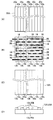
- thermoelectric conversion element of the present invention (A) is a top view conceptually showing an example of the thermoelectric conversion element of the present invention, (B) is the same front view, and (C) is the same bottom view. (A)-(D) are the conceptual diagrams for demonstrating the thermoelectric conversion module using the thermoelectric conversion element of this invention. (A) And (B) is a front view which shows notionally another example of the board
- thermoelectric conversion layer contains predetermined graphene and / or graphene laminate (hereinafter collectively referred to as “graphene-based material”).
- graphene-based materials are materials that exhibit high electrical conductivity and high thermal conductivity. For this reason, it has been conventionally considered to be disadvantageous for improving the thermoelectric conversion performance, but it has been found that a large amount of electric power can be obtained by applying it to a so-called “in plane type” thermoelectric conversion element described later.
- thermoelectric conversion element In FIG. 1, an example of the thermoelectric conversion element of this invention is shown notionally.
- 1A is a top view (a view of FIG. 1B viewed from above),
- FIG. 1B is a front view (a view of a substrate or the like to be described later), and
- FIG. 1C FIG. 2 is a bottom view (a view of FIG. 1B viewed from the lower side of the drawing).
- the thermoelectric conversion element 10 basically includes a first substrate 12, a first adhesion layer 14, a thermoelectric conversion layer 16, a second adhesion layer 18, a second substrate 20, and electrodes. 26 and an electrode 28.
- the first adhesion layer 14 is provided on the first substrate 12
- the thermoelectric conversion layer 16 is provided on the first adhesion layer 14
- the second adhesion layer 18 is provided on the thermoelectric conversion layer 16.
- the second substrate 20 has a second substrate 20 on the second adhesion layer 18.
- thermoelectric conversion layer 16 is arranged in the substrate surface direction of the first substrate 12 and the second substrate 20 (hereinafter referred to as In other words, the electrode 26 and the electrode 28 (electrode pair) are provided on the thermoelectric conversion layer 16 so as to be sandwiched between the first substrate 12 and the second substrate 20. Connected.
- substrate 12 has the low heat conduction part 12a and the high heat conduction part 12b.
- substrate 20 also has the low heat conduction part 20a and the high heat conduction part 20b.
- the two substrates are arranged such that their high thermal conductivity portions are at different positions in the direction in which the electrode 26 and the electrode 28 are separated (that is, in the energization direction).
- substrates have the same structure only in the arrangement position and the direction of front and back, and a surface direction (board
- the first substrate 12 covers a region on one half of one surface of the plate-like material that becomes the low thermal conduction portion 12 a (low thermal conduction portion 20 a). It has a configuration in which the high heat conduction part 12b (high heat conduction part 20b) is laminated. Therefore, on one surface (one surface) of the first substrate 12, a half region in the plane direction is the low heat conduction portion 12a, and the other half region is the high heat conduction portion 12b. In addition, the other surface of the first substrate 12 is the low thermal conductive portion 12a.
- thermoelectric conversion element of this invention various structures can be utilized for the 1st board
- the first substrate is formed with a recess in a half region of one surface of the plate-like material that becomes the low heat conducting portion 12a, The structure which incorporates the high heat conductive part 12b so that may become uniform may be sufficient.
- the first substrate is a laminated body shown in FIG. 1A
- the second substrate is a first substrate and a second substrate, such as a configuration in which a high heat conduction portion is incorporated in the concave portion shown in FIG.
- the method for forming the high thermal conductivity portion may be different.
- thermoelectric conversion element 10 for example, a temperature difference is generated by heating due to contact with a heat source or the like, so that a difference occurs in the carrier density in the direction of the temperature difference in the thermoelectric conversion layer 16 according to the temperature difference.
- Power is generated.
- a heat source is provided on the first substrate 12 side, and a temperature difference is generated between the high heat conduction portion 12b of the first substrate 12 and the high heat conduction portion 20b of the second substrate 20, thereby generating power. To do. Further, by connecting wiring to the electrode 26 and the electrode 28, electric power (electric energy) generated by heating or the like is taken out.
- thermoelectric conversion element 10 of the present invention uses two substrates having a high heat conduction portion and a low heat conduction portion, and places the high heat conduction portions of both substrates in different positions in the plane direction, and sandwiches the thermoelectric conversion layer between the two substrates.
- this configuration is also referred to as “in plane type”
- the thermoelectric conversion layer 16 includes graphene and / or a graphene laminate (graphene-based material) described later, thereby achieving high power generation.
- the thermoelectric conversion element which can obtain quantity is realized.
- the mechanism will be described in detail.
- thermoelectric conversion layer the higher the Seebeck coefficient and the higher the electrical conductivity, the higher the amount of power generated. Therefore, it is conceivable that a thermoelectric conversion element showing a high power generation amount can be obtained by using a graphene-based material for the thermoelectric conversion layer.
- graphene-based materials have high thermal conductivity.
- thermoelectric conversion element for example, a unileg type thermoelectric conversion element
- a normal thermoelectric conversion element has a configuration in which a block-shaped thermoelectric conversion layer is sandwiched between electrodes.
- the temperature difference generated in the thermoelectric conversion layer in the direction in which the electrodes are separated from each other, that is, in the direction in which the electrode pair is separated (hereinafter also referred to as “inter-electrode direction”).
- the graphene-based material has high thermal conductivity.
- thermoelectric conversion layer if a graphene-based material is used for the thermoelectric conversion layer, even if the thermoelectric conversion layer is thick, a temperature difference is very likely to occur in the thermoelectric conversion layer. It is difficult and high power generation cannot be obtained. Therefore, in a normal thermoelectric conversion element in which a block-shaped thermoelectric conversion layer is sandwiched between electrodes, a graphene-based material with high thermal conductivity cannot be used for the thermoelectric conversion layer, and a material with as low a thermal conductivity as possible is used. Thus, a thermoelectric conversion layer is formed.
- the first substrate 12 has a high heat conduction part 12b
- the second substrate 20 has a high heat conduction part 20b
- the high heat conduction part 12b and the high heat conduction part 12b are arranged at a different position in the plane direction without overlapping. Therefore, for example, when a heat source is provided on the first substrate 12 side, a temperature difference is generated in the surface direction of the thermoelectric conversion layer 16 between the high thermal conductivity portion 12b and the high thermal conductivity portion 20b.
- thermoelectric conversion element 10 of the present invention that is an in-plane type
- the heat is applied in the surface direction of the sheet-like thermoelectric conversion layer 16 as conceptually shown by the arrow x in FIGS. Flows. Therefore, the thermoelectric conversion element 10 of the present invention can cause a large temperature difference in the sheet-like thermoelectric conversion layer 16 between the electrodes without increasing the thickness of the thermoelectric conversion layer 16. Further, by making the thermoelectric conversion layer 16 longer in the inter-electrode direction, a higher power generation amount can be obtained due to a temperature difference over a long distance in the surface direction.
- thermoelectric conversion layer 16 is not a block shape but a thin sheet shape.
- thermoelectric conversion element 10 since the heat flow path in the thermoelectric conversion layer 16 is narrow and it is difficult for heat to flow, a temperature difference is easily generated in the thermoelectric conversion layer 16.
- the in-plane thermoelectric conversion element 10 is more likely to cause a temperature difference by making the thermoelectric conversion layer 16 thinner.
- it is easy to improve flexibility That is, by making the thermoelectric conversion element 10 of the present invention in-plane type, even if a graphene-based material with high thermal conductivity is used, a temperature difference can be generated in the thermoelectric conversion layer 16, and a high power generation amount can be obtained. Obtainable.
- each member used for the thermoelectric conversion element 10 will be described in detail.
- the first substrate 12 and the second substrate 20 are disposed on both sides of the thermoelectric conversion layer 16 and each have a low heat conduction portion and a high heat conduction portion.
- the first substrate 12 is used as a representative example.
- the first substrate 12 has a low heat conduction part 12a and a high heat conduction part 12b.
- the low heat conduction part 12a is made of various materials as long as it has insulating properties and sufficient heat resistance to the formation of the thermoelectric conversion layer 16 and the electrode 26, such as a glass plate, a ceramic plate, and a plastic film. A thing consisting of can be used.
- a plastic film is used for the low thermal conductive portion 12a. By using a plastic film for the low heat conducting portion 12a, it is possible to reduce the weight and reduce the cost and to form the flexible thermoelectric conversion element 10, which is preferable.
- a film sheet-like / plate-like
- the film which consists of a polyimide, a polyethylene terephthalate, a polyethylene naphthalate etc. is utilized suitably at points, such as thermal conductivity, heat resistance, solvent resistance, availability, and economical efficiency.
- the film which consists of various materials is illustrated.
- various metals such as gold, silver, copper, and aluminum are exemplified in terms of thermal conductivity and the like.
- copper and aluminum are preferably used in terms of thermal conductivity, economy, and the like.
- the thickness of the first substrate 12, the thickness of the low thermal conductive portion 12 a, and the like are appropriately determined according to the forming material of the high thermal conductive portion 12 b and the low thermal conductive portion 12 a, the size of the thermoelectric conversion element 10, and the like. , You can set.
- substrate 12 is the thickness of the low heat conductive part 12a of the area
- the size in the surface direction of the first substrate 12 (when viewed from the direction orthogonal to the substrate surface), the area ratio in the surface direction of the high heat conduction portion 12b in the substrate 12, and the like are also low heat conduction portions 12a and high heat conduction portions 12b. What is necessary is just to set suitably according to the formation material of this, the magnitude
- the position of the first substrate 12 in the surface direction of the high thermal conductive portion 12b is not limited to the illustrated example, and various positions can be used.
- the high heat conductive part 12b may be included in the low heat conductive part 12a in the surface direction.
- a part of the high heat conduction unit 12b may be located at the end of the first substrate 12 in the plane direction, and the other region may be included in the low heat conduction unit 12a.
- the first substrate 12 may have a plurality of high heat conducting portions 12b in the surface direction.
- thermoelectric conversion element 10 shown in FIG. 1 is a preferable mode in which a temperature difference between the first substrate 12 and the second substrate 20 is likely to occur, and both the first substrate 12 and the second substrate 20 have high thermal conductivity.
- the part 12b and the high heat conduction part 20b are located outside in the stacking direction.
- the present invention may have a configuration in which the first substrate 12 and the second substrate 20 both have the high heat conduction portion 12b and the high heat conduction portion 20b located inside in the stacking direction.
- the first substrate 12 may be configured such that the high heat conductive portion 12b is positioned outside in the stacking direction, and the second substrate 20 is positioned such that the high heat conductive portion 20b is positioned inside in the stacking direction.
- the high thermal conductivity portion is formed of a material having conductivity such as metal and disposed inside the stacking direction, and the first adhesion layer 14 and / or the second adhesion layer 18 are electrically conductive. In order to ensure insulation between the high thermal conductivity portion and the electrodes 26 and 28, an insulating layer or the like may be formed between them.
- thermoelectric conversion element 10 in the illustrated example has a high thermal conductivity between the high thermal conductivity portion 12b of the first substrate 12 and the second substrate 20 so as to face each other in the inter-electrode direction when viewed from a direction orthogonal to the substrate surface.
- the part 20b is arranged at a position different in the surface direction in the inter-electrode direction.
- various configurations can be used for the thermoelectric conversion element of the present invention as long as the high thermal conductivity portion of the first substrate and the high thermal conductivity portion of the second substrate do not completely overlap in the plane direction. is there.
- the high thermal conductivity portion of the first substrate and the high thermal conductivity portion of the second substrate must completely overlap when viewed from a direction perpendicular to the plane direction (substrate plane).
- the high heat conduction part may be placed on the low heat conduction part as shown in FIG. 1 (B), or the low heat conduction part as shown in FIG. 3 (A). You may incorporate in the formed recessed part.
- the high heat conduction part 12 b of the first substrate 12 is moved to the right side in the figure
- the high heat conduction part 20 b of the second substrate 20 is moved to the left side in the figure
- both high heat conduction parts are They may be separated in the inter-electrode direction (plane direction).
- the high heat conduction part 12b of the first substrate 12 and the high heat conduction part 20b of the second substrate 20 are in the plane direction with respect to the size of the thermoelectric conversion layer 16 in the direction in which the electrode 26 and the electrode 28 are separated from each other.
- it is preferably 10 to 90% apart in the direction between the electrodes, and more preferably 10 to 50% apart.
- the high heat conductive portion 12b and / or the high heat conductive portion 20b are provided with a convex portion directed to the other, so that the high heat conductive portions of both the substrates partially overlap in the plane direction. It may be.
- the high heat conduction portion 12b of the first substrate 12 is moved to the left side in the drawing, and the high heat conduction portion 20b of the second substrate 20 is moved to the right side in the drawing, A part of the conductive portion may overlap in the surface direction.
- thermoelectric conversion layer has a temperature difference in the surface direction and a thermoelectricity that causes a temperature difference in the thickness direction. Efficient power generation is possible compared to the conversion element.
- thermoelectric conversion layer 16 is provided on the first substrate 12 via the first adhesion layer 14.
- a second substrate 20 is provided on the thermoelectric conversion layer 16 with a second adhesion layer 18 interposed therebetween. That is, in the thermoelectric conversion element 10, the first adhesion layer 14 is provided between the first substrate 12 and the thermoelectric conversion layer 16, and the second adhesion is provided between the second substrate 20 and the thermoelectric conversion layer 16. Layer 18 is provided. By arranging such an adhesion layer, sufficient adhesion between the thermoelectric conversion layer 16 and the first substrate 12 and the second substrate 20 can be ensured, and after the thermoelectric conversion element 10 is bent or bent.
- thermoelectric conversion element 10 can easily exhibit a desired effect even after being bent or bent, and is excellent in flexibility.
- the thermoelectric conversion element 10 can be obtained and is preferable.
- the first adhesion layer 14 and the second adhesion layer 18 are disposed, but the thermoelectric conversion layer 16 and the first substrate 12 (or the second substrate 20) are sufficiently adhered. In such a case, the adhesion layer may not be disposed.
- the first adhesion layer 14 and the second adhesion layer 18 have sufficient adhesion strength between the first substrate 12 and the second substrate 20 and the thermoelectric conversion layer 16 according to the forming materials of the first substrate 12 and the second substrate 20.
- the material constituting the first adhesion layer 14 and the second adhesion layer 18 can be classified into an inorganic adhesion agent or an organic adhesion agent.
- the inorganic adhesive include alkali metal silicates (for example, sodium silicate) composed of silicate ions, polysilicate ions, and colloidal silica ions, and metal oxides, metal hydroxides, and phosphates as curing agents.
- a material added with a borate a material added with a metal oxide, metal hydroxide, silicate or borate as a curing agent to a first metal phosphate (for example, aluminum phosphate), silicic anhydride A colloid solution material in which fine particles of the above are dispersed in water.
- the sol-gel coating film formed from metal alkoxide can be used as an adhesion layer.
- metal powder and metal salt particles may be added to these inorganic adhesives as fillers.
- plasticizers are added to natural polymers such as starch (eg, dextrin), protein (eg, casein), and natural rubber (eg, latex) as necessary.
- natural polymers such as starch (eg, dextrin), protein (eg, casein), and natural rubber (eg, latex) as necessary.
- thermoplastic resin eg, polyvinyl alcohol, polyvinyl acetal, polyvinyl chloride, polyacrylate, polyvinyl acetate, polyurethane
- thermosetting resin eg, melamine resin, phenol resin, epoxy resin
- elastomer resin eg, Chloroprene rubber, styrene butadiene rubber, nitrile rubber, silicon rubber, urethane rubber
- a material obtained by adding a plasticizer, a curing agent, a filler, and a solvent as necessary.
- the materials for forming the first adhesion layer 14 and the second adhesion layer 18 may be the same or different.
- a method for forming the adhesion layer an optimum method is appropriately selected according to the material to be used.
- a method in which a solution containing the inorganic adhesive or the organic adhesive is applied to a predetermined substrate and dried to form an adhesive layer
- a method in which the adhesive sheet is attached to the predetermined substrate a vapor phase growth method
- a method of forming a film made of a metal oxide are examples of a metal oxide.
- the thickness of the first adhesion layer 14 and the second adhesion layer 18 is sufficient depending on the forming material of the first adhesion layer 14 and the second adhesion layer 18, the size of the first substrate 12 and the second substrate 20, and the like. What is necessary is just to set the thickness which can acquire adhesive force suitably. Among these, 0.1 to 50 ⁇ m is preferable and 1 to 20 ⁇ m is more preferable in terms of the balance between the adhesion between the thermoelectric conversion layer and the substrate and the thinning of the thermoelectric conversion element.
- the first adhesion layer 14 and / or the second adhesion layer 18 may be formed corresponding to the entire surface of the first substrate 12 and the second substrate 20 as in the illustrated example.
- the two substrates 20 may be formed only in a region corresponding to the thermoelectric conversion layer 16.
- thermoelectric conversion layer 16 is a layer having a function of converting heat into electricity.
- a thermoelectric conversion layer (power generation layer) 16 is disposed on the first substrate 12 via the first adhesion layer 14.
- the second substrate 20 is disposed on the thermoelectric conversion layer 16 via the second adhesion layer 18. Note that, as described above, both the substrates have the high heat conduction portion located outside in the stacking direction. Therefore, one surface of the thermoelectric conversion layer 16 faces the surface where the entire surface of the first substrate 12 becomes the low heat conduction portion 12a, and the other surface faces the surface where the entire surface of the second substrate 20 becomes the low heat conduction portion 20a. To do.
- thermoelectric conversion layer 16 is provided in such a manner that the center in the plane direction coincides with the boundary between the low thermal conductivity portion and the high thermal conductivity portion of both substrates.
- the thermoelectric conversion layer 16 is connected to an electrode pair including the electrode 26 and the electrode 28 so as to be sandwiched in the surface direction.
- the thermoelectric conversion layer 16 includes graphene or a graphene laminate.
- the thermoelectric conversion layer 16 may include both graphene and a graphene stack.
- Graphene is a sheet (carbon molecule sheet) in which benzene rings (hexagonal structure of carbon atoms) are regularly arranged in a plane.
- graphene intends a sheet single layer (sheet of carbon molecules of one atomic layer).
- the graphene may be partially oxidized, and may contain, for example, an oxygen functional group such as a carboxyl group, a carbonyl group, a hydroxyl group, or an epoxy group.
- a part of carbon atoms may be substituted with a hetero atom. That is, it may be graphene doped with heteroatoms.
- the kind of the hetero atom is not particularly limited, and examples thereof include a nitrogen atom.
- the graphene laminate is a laminate in which a plurality of the graphenes are laminated.
- the formed graphene stacked body corresponds to so-called graphite.
- the number of graphene layers laminated in the graphene laminate is not particularly limited, but two or more layers are preferable from the viewpoint of handleability, and a laminate of 10 to 200,000 layers is more preferably used.
- Graphene laminates are graphite intercalation compounds in which atoms (metal atoms, metal ions) and molecules (acids, halogen compounds, metal salts, etc.) are inserted (intercalated) between graphenes as guest agents (insertion compounds) (Graphite intercalation compound) may be used.
- the guest agent (insertion compound) is not particularly limited as long as it is a compound that can be inserted between graphenes to widen the interval between graphenes. For example, acids, metals, halogen compounds, metal salt compounds, organometallic compounds , And organic compounds.
- Examples of the acid include carboxylic acids such as nitric acid, hydrochloric acid, sulfuric acid, chromic acid, phosphoric acid, perchloric acid, iodic acid, and alkylaminocarboxylic acid.
- Examples of the metal include alkaline metals such as lithium, potassium, sodium, rubidium and cesium, alkaline earth metals such as magnesium, calcium, barium and scandium, titanium, vanadium, chromium, manganese, iron, cobalt, nickel, copper, Transition metals such as yttrium, samarium, and europium are included.
- halogen compound examples include bromine, iodine chloride, bromine chloride, iodine bromide, iodine fluoride, bromine fluoride, and chlorine fluoride.
- metal salt compound examples include aluminum chloride, magnesium chloride, iron chloride, copper chloride, antimony chloride, molybdenum chloride, arsenic pentafluoride, antimony pentafluoride, niobium pentafluoride, and the like.
- organometallic compounds include complex molecules such as triphenylphosphine rhodium, organozinc compounds, and organotin compounds.
- Organic compounds include hydrocarbon compounds, organic silane compounds, organic amine compounds such as alkylamines and pyridines, organic sulfur compounds such as dimethyl sulfoxide, (meth) acrylic esters, ethylene, propylene And polymerizable compounds such as unsaturated hydrocarbon compounds such as styrene and acrylonitrile.
- the insertion compound may be used alone or in combination of two or more.
- the method for producing the graphite intercalation compound is not particularly limited. For example, JP-A-62-87407, JP-A-2-26820, Advances in Physics, 51, pp. 1-186, 2002, carbon, 2007 It can be produced by known methods described in literatures such as pp. 373-378.
- the content of the graphene and the graphene laminate in the thermoelectric conversion layer is not particularly limited, but the total mass of the graphene and the graphene laminate is 20 mass with respect to the total mass of the thermoelectric conversion layer in that a higher power generation amount is obtained. % Or more is preferable, and 50 mass% or more is more preferable.
- the upper limit is not particularly limited, but may be 100% by mass.
- thermoelectric conversion layer 16 containing a graphene or a graphene laminated body is not restrict
- a graphene laminate is formed on a temporary substrate such as copper or nickel by a chemical vapor deposition method (CVD method) using a hydrocarbon such as methane gas as a carbon source, and transferred to a predetermined substrate.
- CVD method chemical vapor deposition method
- Graphite is dispersed in a solvent with ultrasonic waves, and the produced dispersion (a dispersion containing graphene or a graphene laminate) is applied and dried.
- thermoelectric conversion layer may contain other materials other than the graphite-based material as long as the effects of the present invention are not impaired.
- a resin used as a dispersant a surface activity that adjusts coating properties.
- the agent include bases such as acid, metal salt, Lewis acid compound, oxidizing agent, amine compound such as polyethyleneimine, phosphine compound such as triphenylphosphine, and ammonium salt hydroxide.
- bases such as acid, metal salt, Lewis acid compound, oxidizing agent, amine compound such as polyethyleneimine, phosphine compound such as triphenylphosphine, and ammonium salt hydroxide.
- fine particles such as silica and thickeners such as a silane coupling agent can also be used.
- thermoelectric conversion element 10 of the present invention the thickness of the thermoelectric conversion layer 16, the length in the direction between the electrodes, the length in the direction orthogonal to this length, the size in the surface direction, the area ratio in the surface direction with respect to the substrate, etc. What is necessary is just to set suitably according to the magnitude
- FIG. 1B the length of the thermoelectric conversion layer 16 in the interelectrode direction is L, and the thickness of the thermoelectric conversion layer 16 (size in the stacking direction).
- the aspect ratio of L / T can be appropriately adjusted from the viewpoint of thermoelectric conversion performance, but the aspect ratio of L / T is preferably 4 to 500,000, and is preferably 10 to 10,000. Is more preferably 20 to 500, and particularly preferably 200 to 500.
- the thermoelectric conversion layer 16 is thin, and it is advantageous that the thermoelectric conversion layer 16 is long between the electrodes. is there. Therefore, if the L / T aspect ratio in the thermoelectric conversion layer 16 is within the above range, a large temperature difference can be caused in the thermoelectric conversion layer 16 to obtain a higher power generation amount.
- the length L of the thermoelectric conversion layer 16 is appropriately adjusted based on the number of elements per module area based on the manufacturing process. Since the thermoelectromotive force is increased by increasing the number of elements, the length L is preferably 50 ⁇ m to 5 mm, and more preferably 100 ⁇ m to 1 mm.
- the thickness T of the thermoelectric conversion layer 16 is preferably 0.1 to 100 ⁇ m, more preferably 1 to 50 ⁇ m, and further preferably 1 to 25 ⁇ m from the viewpoint of lowering the resistance value of the element in consideration of the manufacturing process.
- An electrode 26 and an electrode 28 are connected to the thermoelectric conversion layer 16 so as to sandwich the thermoelectric conversion layer 16 in the surface direction.
- the electrode 26 and the electrode 28 can be formed of various materials as long as they have a necessary conductivity.
- materials used as transparent electrodes in various devices such as metal materials such as copper, silver, gold, platinum, nickel, chromium, and copper alloys, and indium tin oxide (ITO) and zinc oxide (ZnO). Etc. are exemplified.
- metal materials such as copper, silver, gold, platinum, nickel, chromium, and copper alloys, and indium tin oxide (ITO) and zinc oxide (ZnO). Etc. are exemplified.
- money, platinum, nickel, a copper alloy etc. are illustrated preferably, Gold, platinum, nickel is illustrated more preferably.
- the thickness and size of the electrode 26 and the electrode 28 may be appropriately set according to the thickness of the thermoelectric conversion layer 16 and the size of the thermoelectric conversion element 10.
- thermoelectric conversion element 10 of the present invention may have a gas barrier layer (passivation layer) for preventing deterioration of the thermoelectric conversion layer 16, the electrode 26, the electrode 28, and the like, if necessary.
- This layer is, for example, between the thermoelectric conversion layer 16 and the first adhesion layer 14 and the second adhesion layer 18, between the first adhesion layer 14 and the first substrate 12, and between the second adhesion layer 18 and the second substrate. 20, or on the outer surface side of the first substrate 12 and the second substrate 20.
- the material constituting the gas barrier layer is not particularly limited, and examples thereof include metal oxides such as silicon oxide and aluminum oxide, oxynitrides such as silicon oxynitride and aluminum oxynitride, and metal oxides or oxynitrides thereof. Examples thereof include hybrid materials with organic compounds (for example, organic polymers).
- the adhesion layer 14 and / or the second adhesion layer 18 is formed of silicon oxide or aluminum oxide, the adhesion layer also functions as a gas barrier layer.
- FIGS. 2A to 2D show an example of a thermoelectric conversion module in which a plurality of such thermoelectric conversion elements 10 of the present invention are connected in series.
- 2A to 2C are top views and FIG. 2D is a front view.
- each of the first substrate 12A and the second substrate 20A has a rectangular plate-like high heat conductive portion that extends in one direction on the surface of a rectangular plate-like low heat conductive material, and a side that contacts the low heat conductive portion of the square pillar. Are arranged in the direction orthogonal to the extending direction of the quadrangular prism at equal intervals.
- the entire surface of one surface is a low heat conductive portion, and the other surface is a low heat conductive portion and a high heat conductive portion extending in one direction. It has a structure formed alternately at equal intervals in the orthogonal direction (see FIGS. 2A, 2C, and 2D).
- the first substrate (second substrate) can use various configurations other than the configuration in which the high thermal conductivity portion is placed on the surface of the low thermal conductivity portion.
- the first substrate has a rectangular plate-shaped low heat conductive material, and a groove extending in one direction is perpendicular to the extending direction. The groove may be formed at equal intervals with the width of the groove, and a high heat conductive material may be incorporated in the groove.
- the thermoelectric conversion layer 16 has a rectangular surface shape, and the entire surface of the first substrate 12A is a surface on the side that is the low thermal conductive portion 12a (see FIG. 2 (D) in a state in which the front and back are reversed in the vertical direction in the drawing), the boundary and the center of the low heat conduction portion 12a and the high heat conduction portion 12b are aligned in the plane direction.
- the size of the thermoelectric conversion layer 16 in the horizontal direction in FIG. 2B (hereinafter, also simply referred to as “lateral direction”) is the same as the width of the high thermal conductive portion 12b.
- the horizontal direction is an alternately arranged direction of the low heat conduction parts 12a and the high heat conduction parts 12b.
- the thermoelectric conversion layer 16 is formed at equal intervals every other boundary with respect to the boundary between the low thermal conductivity portion 12a and the high thermal conductivity portion 12b in the lateral direction. That is, the thermoelectric conversion layer 16 is formed in the horizontal direction at equal intervals with the same interval as the width of the high thermal conduction portion 12b (that is, the size of the thermoelectric conversion layer 16). Further, the thermoelectric conversion layers 16 are arranged such that the rows of the thermoelectric conversion layers 16 arranged at equal intervals in the horizontal direction are arranged at equal intervals in the vertical direction in FIG. 2B (hereinafter also simply referred to as “vertical direction”).
- the up-down direction is the extending direction of the low heat conduction portion 12a and the high heat conduction portion 12b.
- the horizontal arrangement of the thermoelectric conversion layers 16 is shifted in the horizontal direction by the width of the high thermal conduction portion 12b in the columns adjacent in the vertical direction. That is, in the rows adjacent in the vertical direction, the thermoelectric conversion layers 16 are alternately formed by the width of the high thermal conductive portion 12b.
- a first adhesion layer 14 is formed on the entire surface of the first substrate 12A on which the thermoelectric conversion layer 16 is formed.
- thermoelectric conversion layer 16 is connected in series by an electrode 26 (electrode 28).
- electrode 26 electrode 28
- the electrodes 26 are connected to each thermoelectric conversion layer. 16 is provided so as to sandwich it horizontally.
- the thermoelectric conversion layers 16 arranged in the lateral direction are connected by the electrodes 26.
- the thermoelectric conversion layers 16 in the rows adjacent in the vertical direction are connected by the electrodes 26 at the lateral ends of the thermoelectric conversion layers 16.
- thermoelectric conversion layer 16 at one end is connected to the thermoelectric conversion layer 16 at the same end of the upper row.
- thermoelectric conversion layer 16 at the other end is connected to the thermoelectric conversion layer 16 at the same end in the lower row. Thereby, all the thermoelectric conversion layers 16 are connected in series like the one line
- the entire surface of the second substrate 20A is placed on the thermoelectric conversion layer 16 and the electrode 26 with the low heat conductive portion 20a facing downward, and the low heat conductive portion 12a and The second substrate 20A is laminated such that the boundary with the high thermal conductive portion 12b coincides with the first substrate 12A.
- This stacking is performed so that the high thermal conductive portion 12b of the first substrate 12A and the high thermal conductive portion 20b of the second substrate 20A are alternated.
- the second adhesion layer 18 is formed on the thermoelectric conversion layer 16 and the electrode 26 so as to cover the entire first substrate 12A.
- the low thermal conductivity portion 12a of the first substrate 12A and the high thermal conductivity portion 20b of the second substrate 20A are aligned in the plane direction and face each other, and the high thermal conductivity portion 12b of the first substrate 12A and the low thermal conductivity portion of the second substrate 20A. 20a faces in the plane direction.
- the thermoelectric conversion module formed by connecting many thermoelectric conversion elements 10 of this invention in series is comprised.
- thermoelectric conversion layers 16 in the horizontal direction is shifted in the horizontal direction by the width of the high heat conduction portion 12b (that is, the high heat conduction portion 20b) in the columns adjacent in the vertical direction. . That is, in the rows adjacent in the vertical direction, the thermoelectric conversion layers 16 are alternately formed by the width of the high thermal conductive portion 12b. For this reason, the thermoelectric conversion layers 16 connected in series as a single folded line have all the thermoelectric conversion layers 16 in the flow in one direction of the connection direction, and one half of the thermoelectric conversion layers 16 is the high thermal conductivity of the first substrate 12A.
- the portion 12b faces the region of the second substrate 20A only of the low heat conduction portion 20a, and the other half faces the region of only the low heat conduction portion 12a of the first substrate 12A and the high heat conduction portion 20b of the second substrate 20A.
- all the thermoelectric conversion layers 16 are upstream.
- Half of the first substrate 12A faces the region of only the high thermal conductivity portion 12b and the second substrate 20A of the low thermal conductivity portion 20a, and the half of the downstream side of the first substrate 12A of the region of only the low thermal conductivity portion 12a and the second substrate 20A.
- thermoelectric conversion module can appropriately generate power.
- thermoelectric conversion element 10 The manufacturing method of a thermoelectric conversion element of the present invention.
- the manufacturing method of the thermoelectric conversion element of the present invention will be described in detail by explaining an example of the manufacturing method of the thermoelectric conversion element 10 shown in FIG.
- First substrate 12 (12A) having low heat conduction part 12a and high heat conduction part 12b, and second substrate 20 (20A) having low heat conduction part 20a and high heat conduction part 20b are prepared.
- the first substrate 12 and the second substrate 20 may be manufactured by a known method using photolithography, etching, film formation technology, or the like.
- a method of preparing the first substrate 12 and the second substrate 20 by preparing a plate material in which a low heat conductive material and a high heat conductive material are laminated and removing a part of the high heat conductive material by etching or the like is exemplified.
- each of the first substrate 12 and the second substrate 20 has a planar shape in which one surface is a low heat conduction portion over the entire surface, and the other surface is a convex high heat on the planar low heat conduction portion.
- the conductive portion is formed and has unevenness (see FIGS. 1B and 2D).
- a concave portion is formed in a part of the sheet-like low thermal conductive material by etching or the like, and a high thermal conductive portion is formed by vacuum deposition or the like using a mask so as to fill the concave portion.
- a method for producing the second substrate 20 is exemplified. In this case, the first substrate 12 and the second substrate 20 are planar on both sides as shown in FIGS. 1 and 2D (FIG. 3A and FIG. 3B). )reference). Commercially available products can also be used for the first substrate 12 and the second substrate 20.
- the first adhesion layer 14 is formed on the surface of the first substrate 12 on the side where the high thermal conductive portion 12b is not formed.
- the first adhesion layer 14 may be formed by a known method such as a vapor deposition method (vacuum film formation method) such as vacuum deposition or sputtering, a coating method, a printing method, or the like according to the material for forming the first adhesion layer 14. Good.
- the first adhesion layer 14 may be formed using an adhesive sheet or an adhesive.
- thermoelectric conversion layer 16 is formed on the first adhesion layer 14.
- the thermoelectric conversion layer 16 can be manufactured by a known method, and examples thereof include the methods (a) to (e) described above.
- a thermoelectric conversion layer is once formed on a temporary substrate by chemical vapor deposition (CVD), and then the temporary substrate is removed (for example, only the temporary substrate is etched with an etchant). And the obtained thermoelectric conversion layer is transferred (placed) on the first substrate.
- a substrate capable of producing graphene or a graphene laminated body is used, and examples thereof include a substrate (SiO 2 film) on which a catalyst (for example, Ni) is supported on the surface, a copper foil, and the like.
- thermoelectric conversion layer is formed by performing a reduction process.
- a method for producing the dispersion a known method can be adopted. For example, in a solvent, graphite is added in a solvent and, if necessary, after oxidation, a dispersion treatment such as ultrasonic waves is applied, or a supercritical fluid such as ethanol is used. The method of processing is mentioned. A known solvent is used as the solvent to be used.
- a polymer film such as polyimide is subjected to high-temperature decomposition treatment to produce a highly oriented graphite sheet, and if necessary, the guest agent is inserted between graphene layers by a known method, Affixed on the first substrate via an adhesion layer.
- a commercial item about the said highly oriented graphite sheet You may use the same commercial item.
- the electrode 26 and the electrode 28 are formed so as to sandwich the thermoelectric conversion layer 16 in the surface direction.
- the formation of the electrode 26 and the electrode 28 may be performed by a known method according to the material for forming the electrode 26 and the electrode 28.
- the second adhesion layer 18 is formed on the thermoelectric conversion layer 16, the electrode 26, and the electrode 28 corresponding to the entire surface of the first substrate 12 (first adhesion layer 14).
- the second adhesion layer 18 is formed only on the thermoelectric conversion layer 16.
- the second adhesion layer 18 may be formed by a known method similar to that of the first adhesion layer 14 depending on the material for forming the second adhesion layer 18.
- the prepared second substrate 20 is attached to the thermoelectric conversion layer 16 with the side where the high heat conduction portion 20b is not formed, and the thermoelectric conversion element 10 is manufactured.
- thermoelectric conversion element of the present invention can be used for various applications. Examples include various power generation applications such as hot spring thermal generators, solar thermal generators, waste heat generators, and other devices (devices) such as wristwatch power supplies, semiconductor drive power supplies, and small sensor power supplies.
- power generation applications such as hot spring thermal generators, solar thermal generators, waste heat generators, and other devices (devices) such as wristwatch power supplies, semiconductor drive power supplies, and small sensor power supplies.
- sensor element uses such as a thermal sensor and a thermocouple, are illustrated besides a power generation use.
- thermoelectric conversion element As described above, the thermoelectric conversion element and the method for manufacturing the thermoelectric conversion element of the present invention have been described in detail. However, the present invention is not limited to the above-described examples, and various improvements and modifications can be made without departing from the gist of the present invention. Of course, you can go.
- thermoelectric conversion element of the present invention will be described in more detail with reference to specific examples of the present invention.
- present invention is not limited to the following examples.
- thermoelectric conversion material> Preparation of graphene laminate (graphite) dispersion
- 10 g of N-methylpyrrolidone was added to 1 g of ultrapure artificial graphite (manufactured by SEC Carbon Co., Ltd.), and sonicated in an ultrasonic bath for 6 hours.
- the produced dispersion was a uniform dispersion (dispersion of graphene laminate (graphite)) without deposits even after standing for 5 hours.
- the obtained dispersion was applied onto a silicon wafer, and it was confirmed by SEM observation of the dried film that the graphite was in a state where the wall was opened in layers.
- thermoelectric conversion module> (Copper stripe pattern processing)
- FELIOS R-F775 (trade name: polyimide layer thickness: 20 ⁇ m, copper layer thickness: 70 ⁇ m, manufactured by Panasonic Electric Works Co., Ltd.) is used as an adhesive-free copper-clad polyimide substrate (substrate size 30 mm ⁇ 30 mm).
- a copper stripe pattern having a thickness of 200 ⁇ m and a space width of 200 ⁇ m was produced by an etching method.
- the first and second substrates as shown in FIG. 2A, FIG. 2C, and FIG. These two types of substrates were prepared.
- the smooth surface of the first substrate having a copper stripe pattern (surface that is a polyimide layer (surface without a copper stripe portion)) was subjected to corona discharge treatment, and then the following coating solution 1 was applied by a bar coating method. This was dried at 180 ° C. for 1 minute to form an adhesion layer.
- thermoelectric conversion layer On the obtained adhesion layer, the dispersion of the graphene laminate prepared in Synthesis Example 1 is used, and the openings are formed by a metal mask printing method having openings of 200 ⁇ m ⁇ 200 ⁇ m and 200 ⁇ m between the openings. 200 ⁇ m composed of a thermoelectric conversion layer having a thickness of 10 ⁇ m, as shown conceptually in FIG. 1100 patterns of ⁇ 200 ⁇ m were formed. Next, an electrode made of gold having a thickness of 1.5 ⁇ m was manufactured by a vacuum deposition method, and 1100 thermoelectric conversion layers were connected in series as conceptually shown in FIG.
- the automatic press TP700A is attached to the smooth surface (surface which is a polyimide layer) of the first substrate and the second substrate on which the thermoelectric conversion layer is formed via a non-support adhesive sheet SK-2478 (trade name of Soken Chemical Co., Ltd.).
- the thermoelectric conversion module 1 formed by connecting 1100 thermoelectric conversion elements in series was prepared by using and bonding under conditions of a press load of 5 kN.
- the first substrate and the second substrate are laminated with a polyimide layer on the entire surface of the first substrate and the second substrate.
- a certain surface (planar surface) was faced so that the copper stripe portion of the first substrate and the portion without the copper stripe (polyimide portion) of the second substrate coincided in the surface direction.
- thermoelectric conversion module 2 Production of thermoelectric conversion module 2>
- an adhesion layer was formed on the smooth surface (surface that is a polyimide layer) of the first substrate having the copper stripe pattern prepared in Example 1.
- the PGS graphite sheet used in Synthesis Example 2 or the graphite sheet (graphite sheet 1 or graphite sheet 2) intercalated with the inorganic salt produced in Synthesis Example 2 is pressed by an automatic press.
- a thermoelectric conversion layer was prepared by thermocompression bonding at 200 ° C. under a load of 5 kN.
- 1100 SiO 2 films having a film thickness of 1 ⁇ m were formed in a pattern of 200 ⁇ m ⁇ 200 ⁇ m openings and 200 ⁇ m between openings by EB vapor deposition.
- the SiO 2 film was arranged so as to overlap with the half width of the copper stripe pattern of the substrate.
- CF 4 / O 2 (3/1) gas is used, and the thermoelectric conversion layer is dry-etched, thereby opening 200 ⁇ m ⁇ 200 ⁇ m as conceptually shown in FIG.
- a 200 ⁇ m pattern thermoelectric conversion layer between the openings was manufactured.
- an electrode made of gold having a thickness of 1.5 ⁇ m was manufactured by a vacuum deposition method, and 1100 thermoelectric conversion layers were connected in series as conceptually shown in FIG.
- thermoelectric conversion modules 2 to 4 in which 1100 thermoelectric conversion elements are connected in series were manufactured by bonding using an automatic press machine TP700A.
- the first substrate and the second substrate are stacked in the same manner as in Example 1; the thermoelectric conversion layer forming surface of the first substrate and the surface (planar surface) in which the entire surface of the second substrate is a polyimide layer.
- substrate matched in the surface direction.
- thermoelectric conversion modules 2 to 4 were used instead of the thermoelectric conversion module 1. The results are shown in Table 1.
- thermoelectric conversion module of the present invention using a highly oriented pyrolytic graphite sheet (graphite) or a graphite sheet (graphite intercalation compound) obtained by intercalating an inorganic salt with the graphite sheet, also showed excellent power generation.
- thermoelectric conversion module 5 Production of thermoelectric conversion module 5> Instead of coating solution 1, coating solution 2 (a solution obtained by adding acetic acid as a catalyst to a 5% ethanol solution of tetraethyl orthosilicate (TEOS) / 3-glycidoxypropyl-trimethoxysilane (molar ratio 3/1)) was used. An adhesion layer was formed according to the same procedure as in Example 1 except that it was used. Next, according to the procedure similar to Example 2, the thermoelectric conversion module 5 was produced using the PGS graphite sheet. When the power generation amount of the thermoelectric conversion module 5 was measured by the above method, the power generation amount showed an excellent value of 12.1 mW / m 2 .
- TEOS tetraethyl orthosilicate
- thermoelectric conversion module 6 Production of thermoelectric conversion module 6> A thermoelectric conversion module 6 was produced according to the same procedure as in Example 1 except that the adhesion layer was not formed using the coating liquid 1. When the power generation amount of the thermoelectric conversion module 6 was measured by the above method, the power generation amount showed an excellent value of 2.2 mW / m 2 .
- thermoelectric conversion module 7 was produced according to the same procedure as in Example 2 except that the adhesion layer was not formed using the coating liquid 1.
- the power generation amount of the thermoelectric conversion module 7 was measured by the above method, the power generation amount showed an excellent value of 11.5 mW / m 2 .
- thermoelectric conversion layer Peeling of the thermoelectric conversion layer is not observed
- B Peeling is observed in a part of the thermoelectric conversion layer, but it can be used practically
- C The thermoelectric conversion layer peeled off so that it cannot be used practically, Or the whole thermoelectric conversion layer is peeled off
- thermoelectric conversion module (Evaluation of heating / bending durability) A 60 W incandescent bulb was lit in the center of an ABS resin pipe having an outer diameter of 35 mm and an inner diameter of 25 mm. At this time, the ambient temperature was 25 ° C., and the temperature of the pipe surface was 50 ° C. The process of winding the thermoelectric conversion module produced in Examples 1 to 7 on this pipe and holding for 3 minutes was repeated 5 times, then the resistance value of the thermoelectric conversion module was measured, and the resistance change rate was calculated from the following equation. Moreover, the state of the thermoelectric conversion layer was confirmed visually.
- Resistance change rate (increase rate) [(resistance value after durability test) ⁇ (resistance value before durability test)] / (resistance value before durability test) ⁇ 100 (%)
- the rate of resistance change and the state of the thermoelectric conversion layer were evaluated according to the following criteria. The results are shown in Table 3.
- C Resistance change rate is ⁇ 10% or more and cracks are observed in thermoelectric conversion layer
- D Resistance value cannot be measured or peeling is recognized in thermoelectric conversion layer
- thermoelectric conversion module having an adhesion layer had a small resistance change rate (increase rate) in a heating / bending durability test assuming actual use, and no peeling of the thermoelectric conversion layer was observed.
Abstract
本発明は、熱電変換層がより汎用性のある材料を用いて形成され、高い発電量が得られる熱電変換素子、および、この熱電変換素子の製造方法を提供する。本発明の熱電変換素子は、面方向の少なくとも一部に他の領域よりも熱伝導率が高い高熱伝導部を有する第1基板と、第1基板の上に配置される、炭素原子の一部がヘテロ原子で置換されてもよいグラフェン、または、グラフェンが複数積層されてなるグラフェン積層体を含む熱電変換層と、熱電変換層の上に配置される、面方向の少なくとも一部に他の領域よりも熱伝導率が高い高熱伝導部を有し、かつ、面方向において自身の高熱伝導部が第1基板の高熱伝導部と完全には重複しない第2基板と、面方向に熱電変換層を挟むように、熱電変換層に接続される一対の電極とを有することを特徴とする。
Description
本発明は、熱電変換素子に関する。詳しくは、高い発電量が得られる熱電変換素子、および、この熱電変換素子の製造方法に関する。
熱エネルギーと電気エネルギーとを相互に変換することができる熱電変換材料が、熱によって発電する発電素子やペルチェ素子のような熱電変換素子に用いられている。
熱電変換素子は、熱エネルギーを直接電力に変換することができ、可動部を必要としない等の利点を有する。そのため、熱電変換素子を利用する発電装置は、例えば、焼却炉や工場の各種の設備など、排熱される部位に設けることで、動作コストを掛ける必要なく、簡易に電力を得ることができる。
熱電変換素子は、熱エネルギーを直接電力に変換することができ、可動部を必要としない等の利点を有する。そのため、熱電変換素子を利用する発電装置は、例えば、焼却炉や工場の各種の設備など、排熱される部位に設けることで、動作コストを掛ける必要なく、簡易に電力を得ることができる。
熱電変換素子は、一般的に、板状の基板の上に電極を有し、電極の上にブロック状の熱電変換層(発電層)を有し、熱電変換層の上に板状の電極を有してなる構成を有する(いわゆる、π型やuni leg型の熱電変換素子)。
すなわち、通常の熱電変換素子は、電極で熱電変換層を厚さ方向に挟持し、熱電変換層の厚さ方向に温度差を生じさせて、熱エネルギーを電気エネルギーに変換させている。
すなわち、通常の熱電変換素子は、電極で熱電変換層を厚さ方向に挟持し、熱電変換層の厚さ方向に温度差を生じさせて、熱エネルギーを電気エネルギーに変換させている。
これに対し、特許文献1には、高熱伝導部を有する基板を用いることにより、熱電変換層の厚さ方向ではなく、熱電変換層の面方向に温度差を生じさせて、熱エネルギーを電気エネルギーに変換する熱電変換素子が記載されている。
具体的には、特許文献1には、P型材料およびN型材料で形成された熱電変換層の両面に、熱伝導率が異なる2種類の材料で構成された柔軟性を有するフィルム基板を設け、熱伝導率が異なる材料を、基板の外面で、かつ、通電方向の逆位置に位置するように構成した熱電変換素子が記載されている。
具体的には、特許文献1には、P型材料およびN型材料で形成された熱電変換層の両面に、熱伝導率が異なる2種類の材料で構成された柔軟性を有するフィルム基板を設け、熱伝導率が異なる材料を、基板の外面で、かつ、通電方向の逆位置に位置するように構成した熱電変換素子が記載されている。
前述のように、熱電変換素子は、熱電変換層に接続される電極の離間方向、すなわち通電方向に温度差を生じさせることで、発電する。また、この温度差が大きい程、高い発電量を得ることができる。
従って、熱電変換層を電極で挟持してなる構成を有する、一般的な熱電変換素子では、熱電変換層に大きな温度差を生じさせるためには、熱電変換層を電極の挟持方向に厚くする必要がある。
従って、熱電変換層を電極で挟持してなる構成を有する、一般的な熱電変換素子では、熱電変換層に大きな温度差を生じさせるためには、熱電変換層を電極の挟持方向に厚くする必要がある。
これに対して、特許文献1に記載される熱電変換素子は、基板に設けられる高熱伝導部によって熱電変換層の面方向に温度差を生じさせて、熱エネルギーを電気エネルギーに変換する。そのため、薄いシート状の熱電変換層でも熱電変換層を長くすることで、電極間方向に大きな温度差を生じさせることができ、高い発電量が得られる。
一方、特許文献1では、熱電変換層に、CePd3-YbPdなどの希少な金属(レアメタル)を含む合金を用いており、材料の汎用性の点で難点がある。
また、近年、熱電変換素子の発電量のより一層の向上が求められており、発電量の更なる向上も必要であった。
また、近年、熱電変換素子の発電量のより一層の向上が求められており、発電量の更なる向上も必要であった。
本発明の目的は、熱電変換層がより汎用性のある材料を用いて形成され、高い発電量が得られる熱電変換素子、および、この熱電変換素子の製造方法を提供することにある。
本発明者らは、上記課題について鋭意検討した結果、グラフェンおよび/またはグラフェン積層体を含む熱電変換層を使用することにより、所望の効果が得られることを見出した。
より具体的には、以下の構成により上記目的を達成することができることを見出した。
より具体的には、以下の構成により上記目的を達成することができることを見出した。
(1) 面方向の少なくとも一部に他の領域よりも熱伝導率が高い高熱伝導部を有する第1基板と、
第1基板の上に配置される、炭素原子の一部がヘテロ原子で置換されてもよいグラフェン、または、グラフェンが複数積層されてなるグラフェン積層体を含む熱電変換層と、
熱電変換層の上に配置される、面方向の少なくとも一部に他の領域よりも熱伝導率が高い高熱伝導部を有し、かつ、面方向において自身の高熱伝導部が第1基板の高熱伝導部と完全には重複しない第2基板と、
面方向に熱電変換層を挟むように、熱電変換層に接続される一対の電極とを有する、熱電変換素子。
(2) 熱電変換層にグラフェン積層体が含まれ、
グラフェン積層体が、黒鉛または黒鉛層間化合物である、(1)に記載の熱電変換素子。
(3) 第1基板と熱電変換層との間、および、第2基板と熱電変換層との間の少なくとも一方に密着層が介在する、(1)または(2)に記載の熱電変換素子。
(4) 第1基板の高熱伝導部と第2基板の高熱伝導部とが、面方向において、電極の離間方向に異なる位置に設けられる、(1)~(3)のいずれかに記載の熱電変換素子。
(5) 第1基板の高熱伝導部および第2基板の高熱伝導部が、積層方向に対して外面に位置する、(1)~(4)のいずれかに記載の熱電変換素子。
(6) 面方向の少なくとも一部に他の領域よりも熱伝導率が高い高熱伝導部を有する第1基板の上に、炭素原子の一部がヘテロ原子で置換されてもよいグラフェン、または、グラフェンが複数積層されてなるグラフェン積層体を含む熱電変換層を形成する工程、
面方向に挟むようにして、熱電変換層に電極対を接続する工程、および、
熱電変換層の上に、面方向の少なくとも一部に、他の領域よりも熱伝導率が高い高熱伝導部を有し、かつ、面方向において自身の高熱伝導部が第1基板の高熱伝導部と完全には重複しないように第2基板を積層する工程を有する、熱電変換素子の製造方法。
本発明によれば、熱電変換層がより汎用性のある材料を用いて形成され、高い発電量が得られる熱電変換素子、および、この熱電変換素子の製造方法を提供することができる。
以下、本発明の熱電変換素子および熱電変換素子の製造方法について、添付の図面に示される好適実施例を基に詳細に説明する。
なお、本発明の特徴点としては、熱電変換層に所定のグラフェンおよび/またはグラフェン積層体(以後、これらを総称して「グラフェン系材料」とも称する)が含有される点が挙げられる。グラフェン系材料は高い導電率を示すと共に、熱伝導率も高い材料である。そのため、従来、熱電変換性能向上に不利と考えられていたが、後述するいわゆる『in plane型』の熱電変換素子に適用することにより、大きな発電量が得られることを見出している。
なお、本発明の特徴点としては、熱電変換層に所定のグラフェンおよび/またはグラフェン積層体(以後、これらを総称して「グラフェン系材料」とも称する)が含有される点が挙げられる。グラフェン系材料は高い導電率を示すと共に、熱伝導率も高い材料である。そのため、従来、熱電変換性能向上に不利と考えられていたが、後述するいわゆる『in plane型』の熱電変換素子に適用することにより、大きな発電量が得られることを見出している。
<熱電変換素子>
図1に、本発明の熱電変換素子の一例を概念的に示す。なお、図1において、(A)は上面図(図1(B)を紙面上方から見た図)、(B)は正面図(後述する基板等の面方向から見た図)、(C)は底面図(図1(B)を紙面下方から見た図)である。
図1に、本発明の熱電変換素子の一例を概念的に示す。なお、図1において、(A)は上面図(図1(B)を紙面上方から見た図)、(B)は正面図(後述する基板等の面方向から見た図)、(C)は底面図(図1(B)を紙面下方から見た図)である。
図1に示すように、熱電変換素子10は、基本的に、第1基板12と、第1密着層14と、熱電変換層16と、第2密着層18と、第2基板20と、電極26および電極28とを有して構成される。
具体的には、第1基板12の上に第1密着層14を有し、第1密着層14の上に熱電変換層16を有し、熱電変換層16の上に第2密着層18を有し、第2密着層18の上に第2基板20を有する。さらに、第1基板12と第2基板20(第1密着層14と第2密着層18)との間において、熱電変換層16を第1基板12および第2基板20の基板面方向(以下、単に『面方向』とも言う。言い換えれば、第1基板12および第2基板20を積層する方向とは直交する方向。)に挟むようにして、熱電変換層16に電極26および電極28(電極対)が接続される。
具体的には、第1基板12の上に第1密着層14を有し、第1密着層14の上に熱電変換層16を有し、熱電変換層16の上に第2密着層18を有し、第2密着層18の上に第2基板20を有する。さらに、第1基板12と第2基板20(第1密着層14と第2密着層18)との間において、熱電変換層16を第1基板12および第2基板20の基板面方向(以下、単に『面方向』とも言う。言い換えれば、第1基板12および第2基板20を積層する方向とは直交する方向。)に挟むようにして、熱電変換層16に電極26および電極28(電極対)が接続される。
図1に示すように、第1基板12は、低熱伝導部12aおよび高熱伝導部12bを有する。同様に、第2基板20も、低熱伝導部20aおよび高熱伝導部20bを有する。図示例において、両基板は、互いの高熱伝導部が、電極26と電極28との離間方向(すなわち通電方向)に異なる位置となるように配置される。
なお、両基板は、配置位置、および、表裏や面方向(基板面方向)の向きが異なるのみで、構成は同じであるので、第1基板12と第2基板20とを区別する必要が有る場合を除いて、説明は第1基板12を代表例として行う。
なお、両基板は、配置位置、および、表裏や面方向(基板面方向)の向きが異なるのみで、構成は同じであるので、第1基板12と第2基板20とを区別する必要が有る場合を除いて、説明は第1基板12を代表例として行う。
図示例の熱電変換素子10において、第1基板12(第2基板20)は、低熱伝導部12a(低熱伝導部20a)となる板状物の、一方の面の半分の領域を覆うように、高熱伝導部12b(高熱伝導部20b)を積層してなる構成を有する。
従って、第1基板12の一面(一方の表面)は、面方向の半分の領域が低熱伝導部12aで、残りの半分の領域は高熱伝導部12bとなる。また、第1基板12の他方の面は、全面が低熱伝導部12aとなる。
なお、本発明の熱電変換素子において、第1基板(第2基板)は、低熱伝導部の表面に高熱伝導部を積層してなる構成以外にも、各種の構成が利用可能である。例えば、第1基板は、図3(A)に概念的に示すように、低熱伝導部12aとなる板状物の、一方の面の半分の領域に凹部を形成して、この凹部に、表面が均一となるように高熱伝導部12bを組み込んでなる構成でもよい。
さらに、第1基板は図1(A)に示す積層体で、第2基板は図3(A)に示す凹部に高熱伝導部を組み込んでなる構成等、第1基板と第2基板とで、高熱伝導部の形成方法が異なってもよい。
熱電変換素子10は、例えば、熱源との接触などによる加熱によって温度差が生じることにより、この温度差に応じて、熱電変換層16の内部において、この温度差の方向のキャリア密度に差が生じ、電力が発生する。図示例においては、例えば、第1基板12側に熱源を設け、第1基板12の高熱伝導部12bと、第2基板20の高熱伝導部20bとの間に温度差を生じさせることにより、発電する。また、電極26および電極28に配線を接続することにより、加熱等によって発生した電力(電気エネルギー)が取り出される。
本発明の熱電変換素子10は、高熱伝導部および低熱伝導部を有する基板を2枚用い、両基板の高熱伝導部を面方向に異なる位置として、この2枚の基板で熱電変換層を挟持してなる構成(以下、この構成を『in plane型』とも言う)を有し、かつ、熱電変換層16に後述するグラフェンおよび/またはグラフェン積層体(グラフェン系材料)が含まれることにより、高い発電量が得られる熱電変換素子を実現している。
以下、その機構について詳述する。
以下、その機構について詳述する。
まず、グラフェン系材料は、導電率が高く、温度差による発電力が高い(ゼーベック係数も金属に比べ大きい)。
一方、熱電変換層は、ゼーベック係数が大きく、かつ、導電率が高い程、高い発電量が得られる。従って、熱電変換層にグラフェン系材料を用いることにより、高い発電量を示す熱電変換素子が得られることが考えられる。
しかしながら、その反面、グラフェン系材料は、熱伝導率が高い。
一方、熱電変換層は、ゼーベック係数が大きく、かつ、導電率が高い程、高い発電量が得られる。従って、熱電変換層にグラフェン系材料を用いることにより、高い発電量を示す熱電変換素子が得られることが考えられる。
しかしながら、その反面、グラフェン系材料は、熱伝導率が高い。
前述のように、通常の熱電変換素子(例えば、uni leg型の熱電変換素子)は、ブロック状の熱電変換層を電極で挟持してなる構成を有する。このような熱電変換素子では、熱電変換層を厚くすることにより、電極と電極との離間方向すなわち電極対の離間方向(以下、『電極間方向』とも言う)で熱電変換層に生じる温度差を大きくできる。
しかしながら、上述したように、グラフェン系材料は、熱伝導率が高い。そのため、ブロック状の熱電変換層を用いる通常の熱電変換素子では、グラフェン系材料を熱電変換層に用いると、熱電変換層を厚くしても、熱電変換層に温度差を生じさせることが非常に困難で、高い発電量が得られない。
そのため、ブロック状の熱電変換層を電極で挟持してなる通常の熱電変換素子では、熱伝導率が高いグラフェン系材料を熱電変換層に用いることはできず、できるだけ熱伝導率が低い材料を用いて、熱電変換層を形成している。
しかしながら、上述したように、グラフェン系材料は、熱伝導率が高い。そのため、ブロック状の熱電変換層を用いる通常の熱電変換素子では、グラフェン系材料を熱電変換層に用いると、熱電変換層を厚くしても、熱電変換層に温度差を生じさせることが非常に困難で、高い発電量が得られない。
そのため、ブロック状の熱電変換層を電極で挟持してなる通常の熱電変換素子では、熱伝導率が高いグラフェン系材料を熱電変換層に用いることはできず、できるだけ熱伝導率が低い材料を用いて、熱電変換層を形成している。
一方、in plane型である本発明の熱電変換素子10は、第1基板12は高熱伝導部12bを、第2基板20は高熱伝導部20bを、それぞれ有し、かつ、高熱伝導部12bと高熱伝導部20bとは、重複せずに面方向に異なる位置に配置される。従って、例えば、第1基板12側に熱源を設けると、高熱伝導部12bと高熱伝導部20bとの間で、熱電変換層16の面方向に温度差が生じる。すなわち、in plane型である本発明の熱電変換素子10では、図1(A)~図1(C)に矢印xで概念的に示すように、シート状の熱電変換層16の面方向に熱が流れる。
そのため、本発明の熱電変換素子10は熱電変換層16を厚くしなくても、電極間のシート状の熱電変換層16において大きな温度差を生じさせることができる。また、熱電変換層16を電極間方向に長くすることにより、面方向の長い距離の温度差によって、より高い発電量が得られる。
そのため、本発明の熱電変換素子10は熱電変換層16を厚くしなくても、電極間のシート状の熱電変換層16において大きな温度差を生じさせることができる。また、熱電変換層16を電極間方向に長くすることにより、面方向の長い距離の温度差によって、より高い発電量が得られる。
より具体的には、本発明者らの検討によれば、in plane型の熱電変換素子では、グラフェン系材料のように熱伝導率が高い材料で熱電変換層を形成しても、熱電変換層に温度差を生じさせることができる。
水や電気と同様に、熱も、伝わる経路すなわち流路が大きい程、流れ易い。また、熱の流路が短い程、伝熱し易く、流れ方向の温度差が生じ難い。
ここで、in plane型の熱電変換素子10は、熱電変換層16が、ブロック状ではなく薄いシート状である。そのため、in plane型の熱電変換素子10では、熱電変換層16における熱の流路が狭く、熱が流れ難いため、熱電変換層16中において温度差を生じさせ易い。
加えて、前述のように、in plane型の熱電変換素子10は、熱電変換層16を薄くすることで、より温度差を生じさせ易い。また、可撓性も良好にしやすい。
すなわち、本発明の熱電変換素子10は、in plane型とすることにより、熱伝導率が高いグラフェン系材料を用いても、熱電変換層16に温度差を生じさせることができ、高い発電量を得ることができる。
以後、熱電変換素子10に使用される各部材について詳述する。
(第1基板および第2基板)
第1基板12および第2基板20は、上述したように熱電変換層16の両面側に配置され、それぞれ低熱伝導部および高熱伝導部を有する。上述したように、以下の説明では、第1基板12を代表例として行う。
第1基板12は、低熱伝導部12aおよび高熱伝導部12bを有する。
低熱伝導部12aは、ガラス板、セラミックス板、プラスチックフィルムなど、絶縁性を有し、かつ、熱電変換層16や電極26等の形成等に対する十分な耐熱性を有するものであれば、各種の材料からなる物が利用可能である。
好ましくは、低熱伝導部12aには、プラスチックフィルムが利用される。低熱伝導部12aにプラスチックフィルムを用いることにより、軽量化やコストの低下を計ると共に、可撓性を有する熱電変換素子10が形成可能となり、好ましい。
低熱伝導部12aに利用可能なプラスチックフィルムとしては、具体的には、ポリエチレンテレフタレート、ポリエチレンイソフタレート、ポリエチレンナフタレート、ポリブチレンテレフタレート、ポリ(1,4-シクロヘキシレンジメチレンテレフタレート)、ポリエチレン-2,6-フタレンジカルボキシレート等のポリエステル、ポリイミド、ポリカーボネート、ポリプロピレン、ポリエーテルスルホン、シクロオレフィンポリマー、ポリエーテルエーテルケトン(PEEK)、トリアセチルセルロース(TAC)等の樹脂、ガラスエポキシ、液晶性ポリエステル等からなるフィルム(シート状物/板状物)が例示される。
なかでも、熱伝導率、耐熱性、耐溶剤性、入手の容易性や経済性等の点で、ポリイミド、ポリエチレンテレフタレート、ポリエチレンナフタレート等からなるフィルムは、好適に利用される。
なかでも、熱伝導率、耐熱性、耐溶剤性、入手の容易性や経済性等の点で、ポリイミド、ポリエチレンテレフタレート、ポリエチレンナフタレート等からなるフィルムは、好適に利用される。
高熱伝導部12bは、低熱伝導部12aよりも熱伝導率が高いものであれば、各種の材料からなるフィルムが例示される。
具体的には、熱伝導率等の点で、金、銀、銅、アルミニウム等の各種の金属が例示される。なかでも、熱伝導率、経済性等の点で、銅およびアルミニウムが好適に利用される。
具体的には、熱伝導率等の点で、金、銀、銅、アルミニウム等の各種の金属が例示される。なかでも、熱伝導率、経済性等の点で、銅およびアルミニウムが好適に利用される。
なお、本発明において、第1基板12の厚さ、低熱伝導部12aの厚さ等は、高熱伝導部12bおよび低熱伝導部12aの形成材料、熱電変換素子10の大きさ等に応じて、適宜、設定すればよい。なお、第1基板12の厚さとは、高熱伝導部12bが無い領域の低熱伝導部12aの厚さである。
また、第1基板12の面方向(基板面と直交する方向から見た際)の大きさ、基板12における高熱伝導部12bの面方向の面積率等も、低熱伝導部12aおよび高熱伝導部12bの形成材料、熱電変換素子10の大きさ等に応じて、適宜、設定すればよい。
また、第1基板12の面方向(基板面と直交する方向から見た際)の大きさ、基板12における高熱伝導部12bの面方向の面積率等も、低熱伝導部12aおよび高熱伝導部12bの形成材料、熱電変換素子10の大きさ等に応じて、適宜、設定すればよい。
さらに、第1基板12における高熱伝導部12bの面方向の位置も、図示例に限定されず、各種の位置が利用可能である。
例えば、第1基板12において、高熱伝導部12bは、面方向において低熱伝導部12aに内包されてもよい。あるいは、高熱伝導部12bは、面方向において、一部を第1基板12の端部に位置し、それ以外の領域を低熱伝導部12aに内包されてもよい。
さらに、第1基板12は、面方向に複数の高熱伝導部12bを有してもよい。
例えば、第1基板12において、高熱伝導部12bは、面方向において低熱伝導部12aに内包されてもよい。あるいは、高熱伝導部12bは、面方向において、一部を第1基板12の端部に位置し、それ以外の領域を低熱伝導部12aに内包されてもよい。
さらに、第1基板12は、面方向に複数の高熱伝導部12bを有してもよい。
なお、図1に示す熱電変換素子10は、第1基板12と第2基板20との間での温度差を生じ易い好ましい態様として、第1基板12および第2基板20は、共に、高熱伝導部12bおよび高熱伝導部20bを積層方向の外側に位置している。
しかしながら、本発明は、これ以外にも、第1基板12および第2基板20が、共に、高熱伝導部12bおよび高熱伝導部20bを積層方向の内側に位置する構成でもよい。または、第1基板12が高熱伝導部12bを積層方向の外側に位置し、第2基板20が高熱伝導部20bを積層方向の内側に位置するような構成でもよい。
なお、高熱伝導部が金属等の導電率を有する材料で形成され、かつ、積層方向の内側に配置される場合で、かつ、第1密着層14および/または第2密着層18が、導電性を有する場合には、高熱伝導部と、電極26および電極28との絶縁性を確保するために、間に絶縁層等を形成してもよい。
しかしながら、本発明は、これ以外にも、第1基板12および第2基板20が、共に、高熱伝導部12bおよび高熱伝導部20bを積層方向の内側に位置する構成でもよい。または、第1基板12が高熱伝導部12bを積層方向の外側に位置し、第2基板20が高熱伝導部20bを積層方向の内側に位置するような構成でもよい。
なお、高熱伝導部が金属等の導電率を有する材料で形成され、かつ、積層方向の内側に配置される場合で、かつ、第1密着層14および/または第2密着層18が、導電性を有する場合には、高熱伝導部と、電極26および電極28との絶縁性を確保するために、間に絶縁層等を形成してもよい。
図示例の熱電変換素子10は、基板面に直交する方向から見た際に電極間方向において対面して当接するように、第1基板12の高熱伝導部12bと、第2基板20が高熱伝導部20bとが、電極間方向で、面方向の異なる位置に配置される。
本発明の熱電変換素子は、これ以外にも、第1基板の高熱伝導部と、第2基板の高熱伝導部とが、面方向において完全には重複しなければ、各種の構成が利用可能である。言い換えれば、本発明の熱電変換素子は、第1基板の高熱伝導部と第2基板の高熱伝導部とが、面方向(基板面)と直交する方向から見た際に完全には重複しなければ、各種の構成が利用可能である。なお、以下の例においても、高熱伝導部は、図1(B)に示すように低熱伝導部の上に載置されてもよく、または、図3(A)に示すように低熱伝導部に形成した凹部に組み込まれてもよい。
本発明の熱電変換素子は、これ以外にも、第1基板の高熱伝導部と、第2基板の高熱伝導部とが、面方向において完全には重複しなければ、各種の構成が利用可能である。言い換えれば、本発明の熱電変換素子は、第1基板の高熱伝導部と第2基板の高熱伝導部とが、面方向(基板面)と直交する方向から見た際に完全には重複しなければ、各種の構成が利用可能である。なお、以下の例においても、高熱伝導部は、図1(B)に示すように低熱伝導部の上に載置されてもよく、または、図3(A)に示すように低熱伝導部に形成した凹部に組み込まれてもよい。
例えば、図1に示す例において、第1基板12の高熱伝導部12bを図中右側に移動し、第2基板20の高熱伝導部20bを図中左側に移動して、両高熱伝導部を、電極間方向(面方向)に離間させてもよい。具体的には、第1基板12の高熱伝導部12bと第2基板20の高熱伝導部20bとは、面方向において、電極26と電極28との離間方向における熱電変換層16の大きさに対して、電極間方向に10~90%離間させるのが好ましく、10~50%離間させるのがより好ましい。
または、この両高熱伝導部が離間する構成において、高熱伝導部12bおよび/または高熱伝導部20bに、他方に向かう凸部を設け、面方向において、両基板の高熱伝導部が一部重複するようにしてもよい。
または、この両高熱伝導部が離間する構成において、高熱伝導部12bおよび/または高熱伝導部20bに、他方に向かう凸部を設け、面方向において、両基板の高熱伝導部が一部重複するようにしてもよい。
逆に、図1に示す例において、第1基板12の高熱伝導部12bを図中左側に移動し、第2基板20の高熱伝導部20bを図中右側に移動することによって、両基板の高熱伝導部の一部を、面方向で重複させてもよい。
また、例えば、第1基板に円形の高熱伝導部を形成し、第2基板に同サイズ(直径と一辺の長さとが一致)の正方形の高熱伝導部を形成して、両高熱伝導部の中心を面方向で一致させるように、両基板を配置してもよい。この構成でも距離は短いが、両高熱伝導部は、端部(周辺)位置が面方向で異なるので、熱電変換層には面方向の温度差が生じ、厚さ方向に温度差を生じさせる熱電変換素子に比して、効率の良い発電が可能である。
(第1密着層および第2密着層)
熱電変換素子10において、第1基板12の上には、第1密着層14を介して熱電変換層16を有する。また、熱電変換層16の上には、第2密着層18を介して第2基板20を有する。すなわち、熱電変換素子10において、第1基板12と熱電変換層16との間には、第1密着層14が設けられ、第2基板20と熱電変換層16との間には、第2密着層18が設けられる。このような密着層が配置されることにより、熱電変換層16と第1基板12および第2基板20との十分な密着性を確保するたことができ、熱電変換素子10を湾曲または折り曲げた後にも熱電変換層16と第1基板12(または、第2基板20)との間の剥離が生じにくく、湾曲または折り曲げた後でも熱電変換素子10が所望の効果を示しやすく、可撓性により優れる熱電変換素子10を得ることができ、好ましい。なお、図1においては、第1密着層14および第2密着層18を配置しているが、熱電変換層16と第1基板12(または、第2基板20)とが十分に密着している場合は、上記密着層は配置しなくてもよい。
熱電変換素子10において、第1基板12の上には、第1密着層14を介して熱電変換層16を有する。また、熱電変換層16の上には、第2密着層18を介して第2基板20を有する。すなわち、熱電変換素子10において、第1基板12と熱電変換層16との間には、第1密着層14が設けられ、第2基板20と熱電変換層16との間には、第2密着層18が設けられる。このような密着層が配置されることにより、熱電変換層16と第1基板12および第2基板20との十分な密着性を確保するたことができ、熱電変換素子10を湾曲または折り曲げた後にも熱電変換層16と第1基板12(または、第2基板20)との間の剥離が生じにくく、湾曲または折り曲げた後でも熱電変換素子10が所望の効果を示しやすく、可撓性により優れる熱電変換素子10を得ることができ、好ましい。なお、図1においては、第1密着層14および第2密着層18を配置しているが、熱電変換層16と第1基板12(または、第2基板20)とが十分に密着している場合は、上記密着層は配置しなくてもよい。
第1密着層14および第2密着層18は、第1基板12および第2基板20の形成材料に応じて、第1基板12および第2基板20と、熱電変換層16との十分な密着力が得られる材料からなるものが、各種、利用可能である。
第1密着層14および第2密着層18を構成する材料としては、具体的には、無機系密着剤、または、有機系密着剤に分類できる。
無機系密着剤としては、例えば、シリケートイオン、ポリシリケートイオンおよびコロイド状シリカイオンからなるアルカリ金属ケイ酸塩(例えば、ケイ酸ナトリウム)に硬化剤として金属酸化物、金属水酸化物、リン酸塩またはホウ酸塩を添加した材料、第1リン酸金属塩(例えば、リン酸アルミニウム)に硬化剤として金属酸化物、金属水酸化物、ケイ酸塩またはホウ酸塩を添加した材料、無水ケイ酸の微粒子を水分散したコロイド溶液材料が挙げられる。また、金属アルコキシド(例えば、テトラアルコキシシランや、置換基を有するシランカップリング剤など)から形成されるゾルゲル塗膜を密着層として使用できる。これらの無機系密着剤に、耐熱性、熱伝導性、電気伝導性などを向上させる目的で、金属粉、金属塩粒子を充填剤として添加してもよい。
有機系密着剤としては、デンプン(例えば、デキストリン)、タンパク(例えば、ガゼイン)、天然ゴム(例えば、ラテックス)などの天然高分子に、必要に応じ可塑剤、硬化剤、充填剤、溶剤を添加した材料、熱可塑性樹脂(例えば、ポリビニルアルコール、ポリビニルアセタール、ポリ塩化ビニル、ポリアクリレート、ポリ酢酸ビニル、ポリウレタン)、熱硬化性樹脂(例えば、メラミン樹脂、フェノール樹脂、エポキシ樹脂)、エラストマー樹脂(例えば、クロロプレンゴム、スチレンブタジエンゴム、二トリルゴム、シリコンゴム、ウレタンゴム)などの合成高分子に、必要に応じ可塑剤、硬化剤、充填剤、溶剤を添加した材料が挙げられる。
なお、第1密着層14と第2密着層18の形成材料は、同じでも異なってもよい。
密着層を形成する方法は、使用される材料に応じて適宜最適な方法が選択される。上記無機系密着剤または有機系密着剤を含む溶液を所定の基板に塗布、乾燥して密着層を形成する方法、上記密着剤のシートを所定の基板に貼り付ける方法の他、気相成長法により金属酸化物からなる膜を形成する方法などが挙げられる。
第1密着層14および第2密着層18の厚さは、第1密着層14および第2密着層18の形成材料、第1基板12および第2基板20の大きさ等に応じて、十分な密着力を得られる厚さを、適宜、設定すればよい。
なかでも、熱電変換層と基板との密着性、および、熱電変換素子の薄型化のバランスの点で、0.1~50μmが好ましく、1~20μmがより好ましい。
なかでも、熱電変換層と基板との密着性、および、熱電変換素子の薄型化のバランスの点で、0.1~50μmが好ましく、1~20μmがより好ましい。
なお、第1密着層14および/または第2密着層18は、図示例のように、第1基板12および第2基板20の全面に対応して形成してもよく、第1基板12および第2基板20の熱電変換層16に対応する領域のみに形成してもよい。
(熱電変換層)
熱電変換層16は、熱を電気に変換する機能を有する層である。
熱電変換素子10において、第1基板12の上に、第1密着層14を介して熱電変換層(発電層)16が配置される。また、熱電変換層16の上には、第2密着層18を介して第2基板20が配置される。なお、前述のように、両基板は積層方向において、高熱伝導部を外側に位置する。従って、熱電変換層16は、一方の面が第1基板12の全面が低熱伝導部12aとなる面に対面し、他方の面が第2基板20の全面が低熱伝導部20aとなる面に対面する。
熱電変換層16は、面方向の中心を、両基板の低熱伝導部と高熱伝導部との境界に一致して設けられる。
また、熱電変換層16には、面方向に挟むように、電極26および電極28からなる電極対が接続される。
本発明の熱電変換素子10において、熱電変換層16は、グラフェンまたはグラフェン積層体を含む。なお、熱電変換層16には、グラフェンおよびグラフェン積層体の両方が含まれていてもよい。
グラフェンとは、ベンゼン環(炭素原子の六角形構造)が平面状に規則的な並んだシート(炭素分子のシート)である。本明細書では、グラフェンとは、シート単層(1原子層の炭素分子のシート)を意図する。なお、上記グラフェンは、一部が酸化されていてもよく、例えば、カルボキシル基、カルボニル基、ヒドロキシル基、または、エポキシ基等の酸素官能基が含まれていてもよい。
また、上記グラフェンは、炭素原子の一部がヘテロ原子で置換されてもよい。つまり、ヘテロ原子がドープされたグラフェンであってもよい。ヘテロ原子の種類は特に制限されないが、例えば、窒素原子が挙げられる。
グラフェンとは、ベンゼン環(炭素原子の六角形構造)が平面状に規則的な並んだシート(炭素分子のシート)である。本明細書では、グラフェンとは、シート単層(1原子層の炭素分子のシート)を意図する。なお、上記グラフェンは、一部が酸化されていてもよく、例えば、カルボキシル基、カルボニル基、ヒドロキシル基、または、エポキシ基等の酸素官能基が含まれていてもよい。
また、上記グラフェンは、炭素原子の一部がヘテロ原子で置換されてもよい。つまり、ヘテロ原子がドープされたグラフェンであってもよい。ヘテロ原子の種類は特に制限されないが、例えば、窒素原子が挙げられる。
グラフェン積層体とは、上記グラフェンが複数積層されてなる積層体である。例えば、上記グラフェンがヘテロ原子を含まない場合、形成されるグラフェン積層体はいわゆる黒鉛(グラファイト)に該当する。グラフェン積層体において積層されるグラフェンの積層数は特に制限されないが、取り扱い性の点から、2層以上が好ましく、さらに好ましくは10~200,000層の積層体が使用される。
また、グラフェン積層体としては、グラフェン間にゲスト剤(挿入化合物)として原子(金属原子、金属イオン)や分子(酸、ハロゲン化合物、金属塩など)が挿入(インターカレーション)された黒鉛層間化合物(グラファイトインターカレーション化合物)であってもよい。
ゲスト剤(挿入化合物)としては、グラフェン間に挿入させてグラフェン間の間隔を広げることができる化合物であれば、特に限定されないが、例えば、酸、金属、ハロゲン化合物、金属塩化合物、有機金属化合物、および有機化合物などが挙げられる。酸としては、例えば、硝酸、塩酸、硫酸、クロム酸、リン酸、過塩素酸、ヨウ素酸、アルキルアミノカルボン酸などのカルボン酸などが挙げられる。金属としては、例えば、リチウム、カリウム、ナトリウム、ルビジウム、セシウムなどのアルカリ金属、マグネシウム、カルシウム、バリウム、スカンジウムなどのアルカリ土類金属、チタン、バナジウム、クロム、マンガン、鉄、コバルト、ニッケル、銅、イットリウム、サマリウム、ユーロピウムなどの遷移金属などが挙げられる。ハロゲン化合物としては、例えば、臭素、塩化ヨウ素、塩化臭素、臭化ヨウ素、フッ化ヨウ素、フッ化臭素、フッ化塩素が挙げられる。金属塩化合物としては、例えば、塩化アルミニウム、塩化マグネシウム、塩化鉄、塩化銅、塩化アンチモン、塩化モリブデン、五フッ化ヒ素、五フッ化アンチモン、五フッ化ニオブなどが挙げられる。有機金属化合物としては、トリフェニルホスフィンロジウムなどの錯体分子の他、有機亜鉛化合物、有機スズ化合物などが挙げられる。有機化合物としては、炭化水素系化合物、有機シラン系化合物、アルキルアミンやピリジン等の有機アミン系化合物、およびジメチルスルホキシドなどの有機硫黄系化合物などの他、(メタ)アクリル酸エステル類、エチレン、プロピレンなどの不飽和炭化水素化合物、スチレン、アクリロニトリルなどの重合性化合物が挙げられる。
挿入化合物は単独で用いられても2種以上が併用されてもよい。
なお、上記黒鉛層間化合物の製造方法は特に制限されず、例えば、特開昭62-87407公報、特開平2-26820公報、Advances in Physics, 51巻, 1~186頁, 2002年、炭素, 2007年, 373~378頁など文献記載の公知の方法により製造できる。
熱電変換層中における上記グラフェンおよびグラフェン積層体の含有量は特に制限されないが、より高い発電量が得られる点で、熱電変換層全質量に対して、グラフェンおよびグラフェン積層体の合計質量が20質量%以上が好ましく、50質量%以上がより好ましい。上限は特に制限されないが、100質量%が挙げられる。
なお、グラフェンまたはグラフェン積層体を含む熱電変換層16の製造方法は特に制限されず、公知の方法を採用できる。例えば、下記方法を好適な方法として挙げることができるが、これに限定されるものではない。
(a)銅、ニッケルなどの仮基板にメタンガスなどの炭化水素を炭素源とした化学気相成長法(CVD法)によりグラフェン積層体を形成し、所定の基板に転写する。
(b)グラファイトを溶剤中、超音波などで分散し、生成した分散液(グラフェンまたはグラフェン積層体を含む分散液)を塗布、乾燥する。
(c)グラファイトを酸化後、溶剤中で分散、酸化グラフェン化合物として剥離し、生成した酸化グラフェン分散液を塗布、乾燥後、還元処理する。
(d)グラファイトをエタノールなどの超臨界流体により、グラフェン層を剥離、分散させ、生成した分散液を塗布、乾燥する。
(e)ポリイミドなどの高分子フィルムを高温で熱分解し、高配向性のグラファイト化したシートを作製して、必要に応じグラフェン層間にゲスト剤を挿入後、所定の基板に貼り付ける。
また、熱電変換層には、本発明の効果を損なわない範囲で、グラファイト系材料以外の他の材料が含まれていてもよく、例えば、分散剤として使用する樹脂、塗布性を調整する界面活性剤、さらにドーピングにより導電率を調整する酸、金属塩、ルイス酸化合物、酸化剤、ポリエチレンイミンなどのアミン化合物、トリフェニルホスフィンなどのホスフィン化合物、アンモニウム塩のハイドロオキシドなどの塩基が挙げられる。また、粘度を調整するために、シリカなどの微粒子、シランカップリング剤などの増粘剤も用いることができる。
本発明の熱電変換素子10において、熱電変換層16の厚さ、電極間方向の長さ、この長さと直交する方向の長さ、面方向の大きさ、基板に対する面方向の面積率等は、熱電変換素子10の大きさや用途等に応じて、適宜、設定すればよい。
ここで、本発明の熱電変換素子10においては、図1(B)に示すように、電極間方向の熱電変換層16の長さをL、熱電変換層16の厚さ(積層方向のサイズ)をTとした際に、L/Tのアスペクト比を熱電変換性能の観点から適宜調整できるが、L/Tのアスペクト比が4~500,000であるのが好ましく、10~10,000であるのがより好ましく、20~500であるのがさらに好ましく、200~500であるのが特に好ましい。
前述のように、熱電変換層16の電極間方向の温度差を大きくするためには、熱電変換層16が薄い方が有利であり、また、電極間で熱電変換層16が長い方が有利である。そのため、熱電変換層16におけるL/Tのアスペクト比が上記範囲内であれば、熱電変換層16に大きな温度差を生じさせて、より高い発電量を得ることができる。
また、熱電変換層16の長さLは、製造プロセスを踏まえ、モジュール面積当たりの素子の数から適宜調整される。素子数を増やすことで熱起電力が大きくなることから、長さLは50μm~5mmが好ましく、100μm~1mmがより好ましい。
また、熱電変換層16の厚さTは、製造プロセスを勘案し、素子の抵抗値を下げる点から、0.1~100μmが好ましく、1~50μmがより好ましく、1~25μmがさらに好ましい。
また、熱電変換層16の厚さTは、製造プロセスを勘案し、素子の抵抗値を下げる点から、0.1~100μmが好ましく、1~50μmがより好ましく、1~25μmがさらに好ましい。
(電極)
熱電変換層16には、熱電変換層16を面方向に挟持するように、電極26および電極28が接続される。
電極26および電極28は、必要な導電率を有するものであれば、各種の材料で形成可能である。具体的には、銅、銀、金、白金、ニッケル、クロム、銅合金などの金属材料、酸化インジウムスズ(ITO)や酸化亜鉛(ZnO)等の各種のデバイスで透明電極として利用されている材料等が例示される。なかでも、銅、金、白金、ニッケル、銅合金等は好ましく例示され、金、白金、ニッケルはより好ましく例示される。
熱電変換層16には、熱電変換層16を面方向に挟持するように、電極26および電極28が接続される。
電極26および電極28は、必要な導電率を有するものであれば、各種の材料で形成可能である。具体的には、銅、銀、金、白金、ニッケル、クロム、銅合金などの金属材料、酸化インジウムスズ(ITO)や酸化亜鉛(ZnO)等の各種のデバイスで透明電極として利用されている材料等が例示される。なかでも、銅、金、白金、ニッケル、銅合金等は好ましく例示され、金、白金、ニッケルはより好ましく例示される。
また、電極26および電極28の厚さや大きさ等も、熱電変換層16の厚さや、熱電変換素子10の大きさ等に応じて、適宜、設定すればよい。
(その他の構成)
さらに、本発明の熱電変換素子10は、必要に応じて、熱電変換層16や電極26および電極28等の劣化を防止するための、ガスバリア層(パッシベーション層)を有してもよい。
この層は、例えば、熱電変換層16と第1密着層14および第2密着層18との間や、第1密着層14と第1基板12との間および第2密着層18と第2基板20との間、または、第1基板12および第2基板20の外面側等に設ければよい。
ガスバリア層を構成する材料は特に制限されず、例えば、酸化ケイ素、酸化アルミニウムなどの金属酸化物や、酸窒化ケイ素、酸窒化アルミニウムなどの酸窒化物や、これらの金属酸化物または酸窒化物と有機化合物(例えば、有機高分子)とのハイブリッド材料などが挙げられる。
なお、例えば、第1密着層14および/または第2密着層18を酸化ケイ素や酸化アルミニウムで形成した場合には、密着層がガスバリア層としても作用する。
<熱電変換モジュール>
図2(A)~図2(D)に、このような本発明の熱電変換素子10を、複数、直列に接続してなる熱電変換モジュールの一例を示す。なお、図2(A)~図2(C)は上面図、(D)は正面図である。
本例において、第1基板12Aおよび第2基板20Aは、矩形板状の低熱伝導材料の表面に、一方向に延在する四角柱状の高熱伝導部を、四角柱の低熱伝導部に接触する一辺の長さと等間隔で、四角柱の延在方向と直交する方向に配列してなる構成を有する。
すなわち、第1基板12Aおよび第2基板20Aは、一面の表面の全面が低熱伝導部で、他面の表面が、一方向に延在する低熱伝導部と高熱伝導部とが、延在方向と直交する方向に等間隔で交互に形成された構成を有する(図2(A)、図2(C)および図2(D)参照)。
なお、本例においても、第1基板(第2基板)は、低熱伝導部の表面に高熱伝導部を載置した構成以外の、各種の構成が利用可能である。例えば、第1基板は、図3(B)に概念的に示すように、第1基板は、矩形板状の低熱伝導材料に、一方向に延在する溝を、延在方向と直交する方向に溝の幅と等間隔で形成して、この溝に高熱伝導材料を組み込んでなる構成でもよい。
図2(B)および図2(C)に概念的に示すように、熱電変換層16は矩形の面形状を有し、第1基板12Aの全面が低熱伝導部12aである側の表面(図2(D)を図中上下方向に表裏反転した状態)に、低熱伝導部12aと高熱伝導部12bとの境界と中心とを面方向で一致させて形成される。図示例においては、熱電変換層16の図2(B)における横方向(以下、単に『横方向』とも言う)の大きさは、高熱伝導部12bの幅と同じである。なお、言い換えれば、横方向とは、低熱伝導部12aと高熱伝導部12bとの交互の配列方向である。
熱電変換層16は、横方向に、低熱伝導部12aと高熱伝導部12bとの境界に対して、1境界置きに等間隔で形成される。すなわち、熱電変換層16は、横方向に、高熱伝導部12bの幅(すなわち熱電変換層16の大きさ)と同じ間隔で等間隔に形成される。
また、熱電変換層16は、横方向に等間隔に配列された熱電変換層16の列が、図2(B)における上下方向(以下、単に『上下方向』とも言う)、に等間隔で配列されるように、二次元的に形成される。なお、言い換えれば、上下方向とは、低熱伝導部12aと高熱伝導部12bの延在方向である。
さらに、図2(B)に示すように、熱電変換層16の横方向の配列は、上下方向に隣接する列では、高熱伝導部12bの幅だけ、横方向にズレて形成される。すなわち、上下方向に隣接する列では、熱電変換層16は、高熱伝導部12bの幅だけ、互い違いに形成される。
なお、第1基板12Aの熱電変換層16の形成面には、全面に、第1密着層14が形成されている。
各熱電変換層16は、電極26(電極28)によって直列に接続される。具体的には、図2(B)に示すように、図中横方向の熱電変換層16の配列において、電極26(構成を明確にするため、網掛けして示す)が、各熱電変換層16を横方向に挟むように設けられる。これにより、横方向に配列された熱電変換層16が、電極26によって接続される。
さらに、熱電変換層16の横方向の端部では、上下方向に隣接する列の熱電変換層16が、電極26によって接続される。この横方向の列の端部での電極26による上下方向の熱電変換層16の接続は、一方の端部の熱電変換層16は上側の列の同側端部の熱電変換層16と接続され、他方の端部の熱電変換層16は下側の列の同側端部の熱電変換層16と接続される。
これにより、全ての熱電変換層16が、横方向に、複数回、折り返した1本の線のように直列で接続される。
さらに、熱電変換層16の横方向の端部では、上下方向に隣接する列の熱電変換層16が、電極26によって接続される。この横方向の列の端部での電極26による上下方向の熱電変換層16の接続は、一方の端部の熱電変換層16は上側の列の同側端部の熱電変換層16と接続され、他方の端部の熱電変換層16は下側の列の同側端部の熱電変換層16と接続される。
これにより、全ての熱電変換層16が、横方向に、複数回、折り返した1本の線のように直列で接続される。
さらに、図2(A)に概念的に示すように、熱電変換層16および電極26の上に、第2基板20Aの全面が低熱伝導部20a側を下方にして、かつ、低熱伝導部12aと高熱伝導部12bとの境界を第1基板12Aと一致させて、第2基板20Aが積層される。この積層は、第1基板12Aの高熱伝導部12bと第2基板20Aの高熱伝導部20bとが、互い違いになるように行われる。
なお、図示はされないが、第2基板20Aの積層に先立ち、第1基板12Aを全面的に覆うように、熱電変換層16および電極26の上に第2密着層18が形成される。
なお、図示はされないが、第2基板20Aの積層に先立ち、第1基板12Aを全面的に覆うように、熱電変換層16および電極26の上に第2密着層18が形成される。
従って、第1基板12Aの低熱伝導部12aと第2基板20Aの高熱伝導部20bとが面方向に一致して対面し、第1基板12Aの高熱伝導部12bと第2基板20Aの低熱伝導部20aとが面方向に一致して対面する。
これにより、本発明の熱電変換素子10を、多数、直列に接続してなる、熱電変換モジュールが構成される。
これにより、本発明の熱電変換素子10を、多数、直列に接続してなる、熱電変換モジュールが構成される。
ここで、前述のように、熱電変換層16の横方向の配列は、上下方向に隣接する列では、高熱伝導部12b(すなわち高熱伝導部20b)の幅だけ、横方向にズレて形成される。すなわち、上下方向に隣接する列では、熱電変換層16は、高熱伝導部12bの幅だけ、互い違いに形成される。
そのため、折り返した1本の線のように直列に接続された熱電変換層16は、接続方向の一方向の流れにおいて、全ての熱電変換層16が、一方の半分が第1基板12Aの高熱伝導部12bと第2基板20Aの低熱伝導部20aのみの領域とに対面し、他方の半分が第1基板12Aの低熱伝導部12aのみの領域と第2基板20Aの高熱伝導部20bとに対面する。
例えば、図2(B)の上から下への直列の接続方向で見た場合には、図2(A)~図2(C)に示すように、全ての熱電変換層16が、上流側半分が第1基板12Aの高熱伝導部12bおよび第2基板20Aの低熱伝導部20aのみの領域に対面し、下流側の半分が第1基板12Aの低熱伝導部12aのみの領域および第2基板20Aの高熱伝導部20bに対面する。
従って、第1基板12A側または第2基板20A側に熱源を配置した際に、直列に接続された全ての熱電変換層16で、接続方向に対する熱の流れ方向、すなわち発電した電気の流れ方向が一致し、熱電変換モジュールが適正に発電を行うことができる。
<熱電変換素子の製造方法>
以下、図1に示す熱電変換素子10の製造方法の一例を説明することにより、本発明の熱電変換素子の製造方法について詳細に説明する。
以下、図1に示す熱電変換素子10の製造方法の一例を説明することにより、本発明の熱電変換素子の製造方法について詳細に説明する。
低熱伝導部12aおよび高熱伝導部12bを有する第1基板12(12A)、および、低熱伝導部20aおよび高熱伝導部20bを有する第2基板20(20A)を用意する。
第1基板12および第2基板20は、フォトリソグラフィー、エッチング、成膜技術等を利用して、公知の方法で作製すればよい。
例えば、低熱伝導材料と高熱伝導材料とを積層した板材を用意し、高熱伝導材料の一部をエッチング等によって除去して、第1基板12および第2基板20を作製する方法が例示される。この場合には、第1基板12および第2基板20は、一方の面が、全面にわたって低熱伝導部である平面状で、他方の面が、平面状の低熱伝導部の上に凸状の高熱伝導部が形成された、凹凸を有するものとなる(図1(B)および図2(D)参照)。
別の方法として、シート状の低熱伝導材料の一部にエッチング等によって凹部を形成し、この凹部を埋めるように、マスクを用いる真空蒸着等によって高熱伝導部を形成して、第1基板12および第2基板20を作製する方法が例示される。この場合には、第1基板12および第2基板20は、図1や図2(D)等に示されるような、両面が平面状のものとなる(図3(A)および図3(B)参照)。
また、第1基板12および第2基板20は、市販品も利用可能である。
第1基板12の高熱伝導部12bが形成されていない側の表面に、第1密着層14を形成する。
第1密着層14は、第1密着層14の形成材料に応じて、真空蒸着やスパッタリング等の気相堆積法(真空成膜法)、塗布法、印刷法等の公知の方法で形成すればよい。あるいは、接着シートや接着剤を用いて、第1密着層14を形成してもよい。
第1密着層14は、第1密着層14の形成材料に応じて、真空蒸着やスパッタリング等の気相堆積法(真空成膜法)、塗布法、印刷法等の公知の方法で形成すればよい。あるいは、接着シートや接着剤を用いて、第1密着層14を形成してもよい。
次いで、第1密着層14の上に、熱電変換層16を形成する。
熱電変換層16は公知の方法で製造でき、例えば、上記(a)~(e)の方法が挙げられる。
上記方法(a)では、仮基板上に化学気相成長法(CVD法)により熱電変換層を一旦形成して、次に、仮基板を除去して(例えば、仮基板のみをエッチング液にて溶解させ)、得られた熱電変換層を第1基板上に転写(載置)する。仮基板としてはグラフェンまたはグラフェン積層体を製造することができる基板が用いられ、例えば、触媒(例えば、Ni)が表面に担持された基板(SiO2膜)、銅フォイルなどが挙げられる。
また、上記方法(b)~(d)では、グラフェンおよび/またはグラフェン積層体、酸化グラフェンを含む分散液を第1基板上に塗布、乾燥し、酸価グラフェンを使用した場合は必要に応じてさらに還元処理を施すことで熱電変換層を形成する。分散液の製造方法は公知の方法を採用でき、例えば、黒鉛(グラファイト)に溶媒中を加え、必要に応じて酸化後、超音波などの分散処理を施す方法や、エタノールなどの超臨界流体で処理する方法が挙げられる。使用される溶媒は、公知の溶媒が使用される。
上記方法(e)では、ポリイミドなどの高分子フィルムを高温分解処理して、高配向性のグラファイトシートを作製し、必要に応じ、グラフェン層間に上記ゲスト剤を公知の方法で挿入させた後、第1基板上に密着層を介し貼り付ける。なお上記高配向性グラファイトシートについては市販品があり、同市販品を使用してもよい。
次いで、熱電変換層16を面方向で挟むように、電極26および電極28を形成する。
電極26および電極28の形成は、電極26および電極28の形成材料等に応じて、公知の方法で行えばよい。
電極26および電極28の形成は、電極26および電極28の形成材料等に応じて、公知の方法で行えばよい。
次いで、第1基板12(第1密着層14)の全面に対応して、熱電変換層16、電極26および電極28の上に、第2密着層18を形成する。あるいは、熱電変換層16の上のみに、第2密着層18を形成する。
第2密着層18は、第2密着層18の形成材料に応じて、第1密着層14と同様の公知の方法で形成すればよい。
第2密着層18は、第2密着層18の形成材料に応じて、第1密着層14と同様の公知の方法で形成すればよい。
さらに、用意した第2基板20を、高熱伝導部20bが形成されていない側を向けて、熱電変換層16に貼着して、熱電変換素子10を作製する。
このような本発明の熱電変換素子は、各種の用途に利用可能である。
一例として、温泉熱発電機、太陽熱発電機、廃熱発電機などの発電機や、腕時計用電源、半導体駆動電源、小型センサ用電源などの各種装置(デバイス)の電源等、様々な発電用途が例示される。また、本発明の熱電変換素子の用途としては、発電用途以外にも、感熱センサや熱電対などのセンサ素子用途も例示される。
一例として、温泉熱発電機、太陽熱発電機、廃熱発電機などの発電機や、腕時計用電源、半導体駆動電源、小型センサ用電源などの各種装置(デバイス)の電源等、様々な発電用途が例示される。また、本発明の熱電変換素子の用途としては、発電用途以外にも、感熱センサや熱電対などのセンサ素子用途も例示される。
以上、本発明の熱電変換素子および熱電変換素子の製造方法について詳細に説明したが、本発明は上述の例に限定はされず、本発明の要旨を逸脱しない範囲において、各種の改良や変更を行ってもよいのは、もちろんである。
以下、本発明の具体的実施例を挙げて、本発明の熱電変換素子について、より詳細に説明する。ただし、本発明は以下の実施例に限定されるものではない。
<合成例1:熱電変換材料の調製>
(グラフェン積層体(グラファイト)の分散液の作製)
超高純度人造グラファイト(SECカーボン株式会社製)1gにN-メチルピロリドン10gを添加し、超音波バス中で、6時間超音波処理した。生成した分散液は、5時間静置しても沈降物はなく、均一な分散液(グラフェン積層体(グラファイト)の分散液)であった。得られた分散液をシリコンウェハー上に塗布し、乾燥した膜のSEM観察で、グラファイトが層状に壁開した状態であることを確認した。
(グラフェン積層体(グラファイト)の分散液の作製)
超高純度人造グラファイト(SECカーボン株式会社製)1gにN-メチルピロリドン10gを添加し、超音波バス中で、6時間超音波処理した。生成した分散液は、5時間静置しても沈降物はなく、均一な分散液(グラフェン積層体(グラファイト)の分散液)であった。得られた分散液をシリコンウェハー上に塗布し、乾燥した膜のSEM観察で、グラファイトが層状に壁開した状態であることを確認した。
(黒鉛層間化合物の作製)
高配向性熱分解グラファイトであるPGSグラファイトシート(パナソニック株式会社製商品名:厚さ25μm)を使用し、特開昭62-87407号公報に記載の方法に従い、2つのバルブを有するパイレックスガラス管の一方にグラファイトシート、他方に第2塩化鉄(FeCl3)を入れ、真空排気後、電気炉にて300℃、10時間加熱し、グラファイトシート1(黒鉛層間化合物1)を得た。得られたグラファイトシート1のX線回折装置(XRD)測定から、FeCl3がグラフェン間に侵入し、主に第2ステージのインターカレーション状態が生成していることを確認した。
同様にして、第2塩化鉄(FeCl3)の代わりに、塩化第2銅(CuCl2)を使用して、上記と同様の手順に従って、グラファイトシート2(黒鉛層間化合物2)を得た。得られたグラファイトシート2のX線回折装置(XRD)測定から、CuCl2がグラフェン間に侵入し、主に第3ステージのインターカレーション状態が生成していることを確認した。
<実施例1:熱電変換モジュールの作製1>
(銅ストライプパターンの加工)
接着剤フリーの銅張ポリイミド基板(基板サイズ30mm×30mm)として、FELIOS R-F775(パナソニック電工株式会社製商品名:ポリイミド層の厚み:20μm、銅層の厚み:70μm)を用い、銅層幅200μm、スペース幅200μmの銅ストライプパターンをエッチング法により作製した。このとき、互いの銅ストライプ部とスペース部が略一致して重なるにようにして、図2(A)、図2(C)および図2(D)に示すような第1基板と第2基板の2種類の基板を作製した。
(銅ストライプパターンの加工)
接着剤フリーの銅張ポリイミド基板(基板サイズ30mm×30mm)として、FELIOS R-F775(パナソニック電工株式会社製商品名:ポリイミド層の厚み:20μm、銅層の厚み:70μm)を用い、銅層幅200μm、スペース幅200μmの銅ストライプパターンをエッチング法により作製した。このとき、互いの銅ストライプ部とスペース部が略一致して重なるにようにして、図2(A)、図2(C)および図2(D)に示すような第1基板と第2基板の2種類の基板を作製した。
(密着層の形成)
銅ストライプパターンを有する第1基板の平滑面(ポリイミド層である面(銅ストライプ部がない面))を、コロナ放電処理を行った後、下記塗布液1をバーコート法により塗布した。これを180℃で1分間乾燥して密着層を形成した。
銅ストライプパターンを有する第1基板の平滑面(ポリイミド層である面(銅ストライプ部がない面))を、コロナ放電処理を行った後、下記塗布液1をバーコート法により塗布した。これを180℃で1分間乾燥して密着層を形成した。
-塗布液1-
・ポリエチレンメタクリル酸共重合体バインダー:23.3質量部
(三井デュポン(株)製、ニュクリルN410)
・コロイダルシリカ:15.4質量部
(日産化学工業(株)製、スノーテックR503 固形分20質量%)
・エポキシモノマー:221.8質量部
(ナガセケムテックス(株)製、デナコールEX614B 固形分22質量%)
・界面活性剤A:19.5質量部
(三洋化成工業(株)製、ナロアクティーCL-95の1質量%水溶液)
・界面活性剤B:7.7質量部
(日本油脂(株)製、ラピゾールA-90の1質量%水溶液)
・蒸留水:全体が1000質量部になるように添加
・ポリエチレンメタクリル酸共重合体バインダー:23.3質量部
(三井デュポン(株)製、ニュクリルN410)
・コロイダルシリカ:15.4質量部
(日産化学工業(株)製、スノーテックR503 固形分20質量%)
・エポキシモノマー:221.8質量部
(ナガセケムテックス(株)製、デナコールEX614B 固形分22質量%)
・界面活性剤A:19.5質量部
(三洋化成工業(株)製、ナロアクティーCL-95の1質量%水溶液)
・界面活性剤B:7.7質量部
(日本油脂(株)製、ラピゾールA-90の1質量%水溶液)
・蒸留水:全体が1000質量部になるように添加
(熱電変換層の形成)
得られた密着層上に、合成例1で作製したグラフェン積層体の分散液を使用し、開口部200μm×200μm、開口部間の200μmのメタルマスク印刷法により、開口部が基板の銅ストライプパターンの1/2幅に重なるような位置に合わせて重ね塗り印刷し、真空下、加熱乾燥することにより、図2(B)に概念的に示すように、膜厚10μmの熱電変換層から成る200μm×200μmのパターン1100個を形成した。
次に、真空蒸着法により、厚さ1.5μmの金からなる電極を作製して、図2(B)に概念的に示すように、1100個の熱電変換層を直列に接続した。
得られた密着層上に、合成例1で作製したグラフェン積層体の分散液を使用し、開口部200μm×200μm、開口部間の200μmのメタルマスク印刷法により、開口部が基板の銅ストライプパターンの1/2幅に重なるような位置に合わせて重ね塗り印刷し、真空下、加熱乾燥することにより、図2(B)に概念的に示すように、膜厚10μmの熱電変換層から成る200μm×200μmのパターン1100個を形成した。
次に、真空蒸着法により、厚さ1.5μmの金からなる電極を作製して、図2(B)に概念的に示すように、1100個の熱電変換層を直列に接続した。
(基板の貼り合せ)
熱電変換層を形成した第1基板と、第2基板の平滑面(ポリイミド層である面)を、ノンサポート接着シートSK-2478(綜研化学株式会社商品名)を介して、自動プレス機TP700Aを用い、プレス荷重5kNの条件で接着することで、1100個の熱電変換素子を直列に接続してなる熱電変換モジュール1を作製した。
なお、第1基板と第2基板との積層は、図2(A)~図2(C)に示すように、第1基板の熱電変換層形成面と、第2基板の全面がポリイミド層である面(平面状の面)とを対面して、第1基板の銅ストライプ部と第2基板の銅ストライプが無い部分(ポリイミド部)とが面方向で一致するように行った。
熱電変換層を形成した第1基板と、第2基板の平滑面(ポリイミド層である面)を、ノンサポート接着シートSK-2478(綜研化学株式会社商品名)を介して、自動プレス機TP700Aを用い、プレス荷重5kNの条件で接着することで、1100個の熱電変換素子を直列に接続してなる熱電変換モジュール1を作製した。
なお、第1基板と第2基板との積層は、図2(A)~図2(C)に示すように、第1基板の熱電変換層形成面と、第2基板の全面がポリイミド層である面(平面状の面)とを対面して、第1基板の銅ストライプ部と第2基板の銅ストライプが無い部分(ポリイミド部)とが面方向で一致するように行った。
<発電量の測定>
ホットプレート上で加熱した第1の銅プレートと、冷水循環装置(水温25度)と接続した第2の銅プレートの間に、作製した熱電変換モジュール1を設置し、銅プレート間の温度差が10℃になるように、ホットプレートの温度を調整した。熱電変換モジュール1中の直列に接続した最上流の熱電変換層の電極および最下流の熱電変換層の電極と、ソースメーター2450(ケースレー社商品名)とを接続し、開放電圧と短絡電流を計測し、下記式から算出した発電量を算出した。発電量は2.1mW/m2であり、グラフェン積層体を使用し作製した本発明の熱電変換モジュールは良好な発電量を示した。
(発電量)=0.25×(開放電圧)×(短絡電流)
ホットプレート上で加熱した第1の銅プレートと、冷水循環装置(水温25度)と接続した第2の銅プレートの間に、作製した熱電変換モジュール1を設置し、銅プレート間の温度差が10℃になるように、ホットプレートの温度を調整した。熱電変換モジュール1中の直列に接続した最上流の熱電変換層の電極および最下流の熱電変換層の電極と、ソースメーター2450(ケースレー社商品名)とを接続し、開放電圧と短絡電流を計測し、下記式から算出した発電量を算出した。発電量は2.1mW/m2であり、グラフェン積層体を使用し作製した本発明の熱電変換モジュールは良好な発電量を示した。
(発電量)=0.25×(開放電圧)×(短絡電流)
<実施例2~4:熱電変換モジュール2の作製>
実施例1で作製した銅ストライプパターンを有する第1基板の平滑面(ポリイミド層である面)に、実施例2と同様にして、密着層を形成した。この密着層上に、合成例2で使用したPGSグラファイトシート、または、合成例2で製造された無機塩をインターカレーションしたグラファイトシート(グラファイトシート1またはグラファイトシート2)を、自動プレス機でプレス荷重5kN下、200℃で熱圧着させ貼り付けて、熱電変換層を作製した。
これらグラファイトシート上に、EB蒸着法により、クロムマスクを介して膜厚1μmのSiO2膜を、開口部200μm×200μm、開口部間の200μmのパターン状に1100個を形成した。SiO2膜は基板の銅ストライプパターンの1/2幅に重なるように配置した。
SiO2膜をマスクに、CF4/O2(3/1)ガスを使用し、熱電変換層をドライエッチングすることで、図2(B)に概念的に示すように、開口部200μm×200μm、開口部間の200μmのパターン熱電変換層を製造した。
次に、真空蒸着法により、厚さ1.5μmの金からなる電極を作製して、図2(B)に概念的に示すように、1100個の熱電変換層を直列に接続した。
(基板の貼り合せ)
実施例1と同様にして、熱電変換層を形成した第1基板と、第2基板の平滑面(ポリイミド層である面)を、ノンサポート接着シートSK-2478(綜研化学株式会社商品名)を介して、自動プレス機TP700Aを用いて接着することで、1100個の熱電変換素子を直列に接続してなる熱電変換モジュール2~4を作製した。
なお、第1基板と第2基板との積層は、実施例1と同様に、第1基板の熱電変換層形成面と、第2基板の全面がポリイミド層である面(平面状の面)とを対面して、第1基板の銅ストライプ部と第2基板の銅ストライプが無い部分(ポリイミド部)とが面方向で一致するように行った。
実施例1と同様にして、熱電変換層を形成した第1基板と、第2基板の平滑面(ポリイミド層である面)を、ノンサポート接着シートSK-2478(綜研化学株式会社商品名)を介して、自動プレス機TP700Aを用いて接着することで、1100個の熱電変換素子を直列に接続してなる熱電変換モジュール2~4を作製した。
なお、第1基板と第2基板との積層は、実施例1と同様に、第1基板の熱電変換層形成面と、第2基板の全面がポリイミド層である面(平面状の面)とを対面して、第1基板の銅ストライプ部と第2基板の銅ストライプが無い部分(ポリイミド部)とが面方向で一致するように行った。
(発電量の測定)
熱電変換モジュール1の代わりに熱電変換モジュール2~4を使用した以外は、上述した方法に従って、発電量を測定した。結果を表1に示す。
熱電変換モジュール1の代わりに熱電変換モジュール2~4を使用した以外は、上述した方法に従って、発電量を測定した。結果を表1に示す。

表1に示すように、高配向性熱分解グラファイトシート(黒鉛)や、同グラファイトシートに無機塩をインターカレーションさせたグラファイトシート(黒鉛層間化合物)を用いた本発明の熱電変換モジュールは、何れも優れた発電量を示した。
<実施例5:熱電変換モジュール5の作製>
塗布液1の代わりに、塗布液2(オルト珪酸テトラエチル(TEOS)/3-グリシドキシプロピル-トリメトキシシラン(モル比3/1)の5%エタノール溶液に触媒として酢酸を添加した溶液)を用いた以外は、上記実施例1と同様の手順に従って、密着層を形成した。
次に、実施例2と同様の手順に従って、PGSグラファイトシートを用いて、熱電変換モジュール5を作製した。熱電変換モジュール5の発電量を上記方法にて測定したところ、発電量は12.1mW/m2と優れた値を示した。
塗布液1の代わりに、塗布液2(オルト珪酸テトラエチル(TEOS)/3-グリシドキシプロピル-トリメトキシシラン(モル比3/1)の5%エタノール溶液に触媒として酢酸を添加した溶液)を用いた以外は、上記実施例1と同様の手順に従って、密着層を形成した。
次に、実施例2と同様の手順に従って、PGSグラファイトシートを用いて、熱電変換モジュール5を作製した。熱電変換モジュール5の発電量を上記方法にて測定したところ、発電量は12.1mW/m2と優れた値を示した。
<実施例6:熱電変換モジュール6の作製>
塗布液1を用いて密着層を形成することを実施しなかった以外は、実施例1と同様の手順に従って、熱電変換モジュール6を作製した。
熱電変換モジュール6の発電量を上記方法にて測定したところ、発電量は2.2mW/m2と優れた値を示した。
塗布液1を用いて密着層を形成することを実施しなかった以外は、実施例1と同様の手順に従って、熱電変換モジュール6を作製した。
熱電変換モジュール6の発電量を上記方法にて測定したところ、発電量は2.2mW/m2と優れた値を示した。
<実施例7:熱電変換モジュール7の作製>
塗布液1を用いて密着層を形成することを実施しなかった以外は、実施例2と同様の手順に従って、熱電変換モジュール7を作製した。
熱電変換モジュール7の発電量を上記方法にて測定したところ、発電量は11.5mW/m2と優れた値を示した。
塗布液1を用いて密着層を形成することを実施しなかった以外は、実施例2と同様の手順に従って、熱電変換モジュール7を作製した。
熱電変換モジュール7の発電量を上記方法にて測定したところ、発電量は11.5mW/m2と優れた値を示した。
(密着性の評価)
上記実施例1~7で作製した第2基板を貼り合わせる前の第1基板上の熱電変換層に、セロテープ(登録商標)(幅12mm)「CT-12」(ニチバン製)を貼り付けた。次に、剥離時に第1基板とセロテープの角度を135度となるように、セロテープを剥がした。熱電変換層の密着性に対し、セロテープ剥離後の熱電変換層の状態を、下記基準を基に評価した。結果を表2に示す。
A:熱電変換層の剥離がみられない
B:熱電変換層の一部に剥離が認められるが、実用上使用可能であるもの
C:実用上使用できないほど多くの熱電変換層が剥離したもの、または、熱電変換層の全部が剥離したもの
上記実施例1~7で作製した第2基板を貼り合わせる前の第1基板上の熱電変換層に、セロテープ(登録商標)(幅12mm)「CT-12」(ニチバン製)を貼り付けた。次に、剥離時に第1基板とセロテープの角度を135度となるように、セロテープを剥がした。熱電変換層の密着性に対し、セロテープ剥離後の熱電変換層の状態を、下記基準を基に評価した。結果を表2に示す。
A:熱電変換層の剥離がみられない
B:熱電変換層の一部に剥離が認められるが、実用上使用可能であるもの
C:実用上使用できないほど多くの熱電変換層が剥離したもの、または、熱電変換層の全部が剥離したもの

表2に示すように、密着層を設けた場合、熱電変換層の密着性がより優れることが確認された。なお、実施例3と4との比較より、ゲスト剤がFeCl3の場合、密着性により優れることが確認された。
(加熱/曲げ耐久性の評価)
外径φ35mm、内径φ25mmのABS樹脂製パイプの内部中央に、60Wの白熱球を点灯させた。このとき、周囲の温度は25℃、パイプ表面の温度は50℃であった。このパイプに上記実施例1~7で作製した熱電変換モジュールを巻き付け、3分間保持する工程を5回繰り返した後、熱電変換モジュールの抵抗値を測定し、抵抗変化率を下記式より算出した。また、熱電変換層の状態を目視で確認した。
抵抗変化率(増加率)=[(耐久性試験後の抵抗値)-(耐久性試験前の抵抗値)]/(耐久性試験前の抵抗値)×100 (%)
加熱/曲げ耐久性は、抵抗変化率および熱電変換層の状態を、下記基準により、評価した。結果を表3に示す。
A:抵抗変化率が±2%未満で、かつ、熱電変換層の剥離がないもの
B:抵抗変化率が±2%以上±10%未満で、かつ、熱電変換層の剥離がないもの
C:抵抗変化率が±10%以上で、かつ、熱電変換層にひび割れが認められるもの
D:抵抗値を測定できない、または、熱電変換層に剥離が認められるもの

表3に示すように、密着層を有する熱電変換モジュールは、実使用を想定した加熱/曲げ耐久性試験において抵抗変化率(増加率)が小さく、しかも熱電変換層の剥離も認められなかった。
10 熱電変換素子
12,12A 第1基板
12a,20a 低熱伝導部
12b,20b 高熱伝導部
14 第1密着層
16 熱電変換層
18 第2密着層
20,20A 第2基板
26,28 電極
12,12A 第1基板
12a,20a 低熱伝導部
12b,20b 高熱伝導部
14 第1密着層
16 熱電変換層
18 第2密着層
20,20A 第2基板
26,28 電極
Claims (6)
- 面方向の少なくとも一部に他の領域よりも熱伝導率が高い高熱伝導部を有する第1基板と、
前記第1基板の上に配置される、炭素原子の一部がヘテロ原子で置換されてもよいグラフェン、または、前記グラフェンが複数積層されてなるグラフェン積層体を含む熱電変換層と、
前記熱電変換層の上に配置される、面方向の少なくとも一部に他の領域よりも熱伝導率が高い高熱伝導部を有し、かつ、面方向において自身の前記高熱伝導部が前記第1基板の高熱伝導部と完全には重複しない第2基板と、
面方向に前記熱電変換層を挟むように、前記熱電変換層に接続される一対の電極とを有する、熱電変換素子。 - 前記熱電変換層に前記グラフェン積層体が含まれ、
前記グラフェン積層体が、黒鉛または黒鉛層間化合物である、請求項1に記載の熱電変換素子。 - 前記第1基板と前記熱電変換層との間、および、前記第2基板と前記熱電変換層との間の少なくとも一方に密着層が介在する、請求項1または2に記載の熱電変換素子。
- 前記第1基板の高熱伝導部と前記第2基板の高熱伝導部とが、面方向において、前記電極の離間方向に異なる位置に設けられる、請求項1~3のいずれか1項に記載の熱電変換素子。
- 前記第1基板の高熱伝導部および前記第2基板の高熱伝導部が、積層方向に対して外面に位置する、請求項1~4のいずれか1項に記載の熱電変換素子。
- 面方向の少なくとも一部に他の領域よりも熱伝導率が高い高熱伝導部を有する第1基板の上に、炭素原子の一部がヘテロ原子で置換されてもよいグラフェン、または、前記グラフェンが複数積層されてなるグラフェン積層体を含む熱電変換層を形成する工程、
面方向に挟むようにして、前記熱電変換層に電極対を接続する工程、および、
前記熱電変換層の上に、面方向の少なくとも一部に、他の領域よりも熱伝導率が高い高熱伝導部を有し、かつ、面方向において自身の前記高熱伝導部が前記第1基板の高熱伝導部と完全には重複しないように第2基板を積層する工程を有する、熱電変換素子の製造方法。
Priority Applications (1)
| Application Number | Priority Date | Filing Date | Title |
|---|---|---|---|
| JP2016514868A JPWO2015163178A1 (ja) | 2014-04-25 | 2015-04-13 | 熱電変換素子および熱電変換素子の製造方法 |
Applications Claiming Priority (2)
| Application Number | Priority Date | Filing Date | Title |
|---|---|---|---|
| JP2014091118 | 2014-04-25 | ||
| JP2014-091118 | 2014-04-25 |
Publications (1)
| Publication Number | Publication Date |
|---|---|
| WO2015163178A1 true WO2015163178A1 (ja) | 2015-10-29 |
Family
ID=54332345
Family Applications (1)
| Application Number | Title | Priority Date | Filing Date |
|---|---|---|---|
| PCT/JP2015/061332 WO2015163178A1 (ja) | 2014-04-25 | 2015-04-13 | 熱電変換素子および熱電変換素子の製造方法 |
Country Status (2)
| Country | Link |
|---|---|
| JP (1) | JPWO2015163178A1 (ja) |
| WO (1) | WO2015163178A1 (ja) |
Cited By (3)
| Publication number | Priority date | Publication date | Assignee | Title |
|---|---|---|---|---|
| CN110235261A (zh) * | 2017-01-27 | 2019-09-13 | 琳得科株式会社 | 挠性热电转换元件及其制造方法 |
| JP2020516211A (ja) * | 2016-12-22 | 2020-05-28 | ボード オブ トラスティーズ オブ ザ ユニバーシティ オブ アーカンソー | エネルギー採取装置及びセンサならびにそれらの製造及び使用方法 |
| US11705756B2 (en) | 2020-04-22 | 2023-07-18 | Board Of Trustees Of The University Of Arkansas | Device for ambient thermal and vibration energy harvesting |
Citations (6)
| Publication number | Priority date | Publication date | Assignee | Title |
|---|---|---|---|---|
| JP2003133600A (ja) * | 2001-10-24 | 2003-05-09 | Kitagawa Ind Co Ltd | 熱電変換部材及びその製造方法 |
| JP2006186255A (ja) * | 2004-12-28 | 2006-07-13 | Nagaoka Univ Of Technology | 熱電変換素子 |
| JP2008182160A (ja) * | 2007-01-26 | 2008-08-07 | Nippon Steel Chem Co Ltd | フレキシブル熱電変換素子及びその製造方法 |
| JP2011035203A (ja) * | 2009-08-03 | 2011-02-17 | Fujitsu Ltd | 熱電変換モジュール |
| US20130139865A1 (en) * | 2011-12-01 | 2013-06-06 | Samsung Electronics Co., Ltd. | Composite structure of graphene and polymer and method of manufacturing the same |
| WO2013100716A1 (en) * | 2011-12-30 | 2013-07-04 | Samsung Electronics Co., Ltd. | Heterogeneous laminate including graphene, and thermoelectric material, thermoelectric module, and thermoelectric apparatus including the heterogeneous laminate |
Family Cites Families (3)
| Publication number | Priority date | Publication date | Assignee | Title |
|---|---|---|---|---|
| JP2006140334A (ja) * | 2004-11-12 | 2006-06-01 | Canon Inc | 熱電変換素子 |
| JP4770973B2 (ja) * | 2009-09-25 | 2011-09-14 | ダイキン工業株式会社 | 熱交換器 |
| JP5912855B2 (ja) * | 2012-05-23 | 2016-04-27 | 富士通コンポーネント株式会社 | タッチパネル |
-
2015
- 2015-04-13 WO PCT/JP2015/061332 patent/WO2015163178A1/ja active Application Filing
- 2015-04-13 JP JP2016514868A patent/JPWO2015163178A1/ja active Pending
Patent Citations (6)
| Publication number | Priority date | Publication date | Assignee | Title |
|---|---|---|---|---|
| JP2003133600A (ja) * | 2001-10-24 | 2003-05-09 | Kitagawa Ind Co Ltd | 熱電変換部材及びその製造方法 |
| JP2006186255A (ja) * | 2004-12-28 | 2006-07-13 | Nagaoka Univ Of Technology | 熱電変換素子 |
| JP2008182160A (ja) * | 2007-01-26 | 2008-08-07 | Nippon Steel Chem Co Ltd | フレキシブル熱電変換素子及びその製造方法 |
| JP2011035203A (ja) * | 2009-08-03 | 2011-02-17 | Fujitsu Ltd | 熱電変換モジュール |
| US20130139865A1 (en) * | 2011-12-01 | 2013-06-06 | Samsung Electronics Co., Ltd. | Composite structure of graphene and polymer and method of manufacturing the same |
| WO2013100716A1 (en) * | 2011-12-30 | 2013-07-04 | Samsung Electronics Co., Ltd. | Heterogeneous laminate including graphene, and thermoelectric material, thermoelectric module, and thermoelectric apparatus including the heterogeneous laminate |
Non-Patent Citations (1)
| Title |
|---|
| VERMA R ET AL.: "Thermoelectric performance of a single-layer graphene sheet for energy harvesting", IEEE TRANSACTIONS ON ELECTRON DEVICES, vol. 60, no. 6, June 2013 (2013-06-01), pages 2064 - 2070, XP011510334 * |
Cited By (5)
| Publication number | Priority date | Publication date | Assignee | Title |
|---|---|---|---|---|
| JP2020516211A (ja) * | 2016-12-22 | 2020-05-28 | ボード オブ トラスティーズ オブ ザ ユニバーシティ オブ アーカンソー | エネルギー採取装置及びセンサならびにそれらの製造及び使用方法 |
| JP7209627B2 (ja) | 2016-12-22 | 2023-01-20 | ボード オブ トラスティーズ オブ ザ ユニバーシティ オブ アーカンソー | エネルギー採取装置及びセンサならびにそれらの製造及び使用方法 |
| CN110235261A (zh) * | 2017-01-27 | 2019-09-13 | 琳得科株式会社 | 挠性热电转换元件及其制造方法 |
| CN110235261B (zh) * | 2017-01-27 | 2023-07-25 | 琳得科株式会社 | 挠性热电转换元件及其制造方法 |
| US11705756B2 (en) | 2020-04-22 | 2023-07-18 | Board Of Trustees Of The University Of Arkansas | Device for ambient thermal and vibration energy harvesting |
Also Published As
| Publication number | Publication date |
|---|---|
| JPWO2015163178A1 (ja) | 2017-04-13 |
Similar Documents
| Publication | Publication Date | Title |
|---|---|---|
| Ma et al. | Graphene‐based transparent conductive films: material systems, preparation and applications | |
| JP6247771B2 (ja) | 熱電変換素子および熱電変換モジュール | |
| JP5493562B2 (ja) | 熱電変換モジュール | |
| JP6181206B2 (ja) | 熱電変換素子および熱電変換素子の製造方法 | |
| JP6488017B2 (ja) | 熱電変換モジュール、熱電変換モジュールの製造方法および熱伝導性基板 | |
| JP6417050B2 (ja) | 熱電変換モジュール | |
| JP2008060488A (ja) | 片面電極型熱電変換モジュール | |
| JP2013211212A (ja) | 積層電極とその製造方法およびそれ用いた光電変換素子 | |
| JP2014146640A (ja) | 熱電変換部材 | |
| KR101685791B1 (ko) | 도선 및 반도체 소자 배선용 나노 카본 재료 및 육방정계 질화붕소 적층구조물 및 이의 제조 방법 | |
| WO2015163178A1 (ja) | 熱電変換素子および熱電変換素子の製造方法 | |
| US20180182947A1 (en) | Thermoelectric conversion device | |
| JP2016187008A (ja) | 熱電変換デバイス | |
| WO2017038831A1 (ja) | 熱電変換素子および熱電変換モジュール | |
| KR20130120627A (ko) | 그래핀을 이용한 발열유리 및 그 제조방법 | |
| US20180183360A1 (en) | Thermoelectric conversion module | |
| JP6431992B2 (ja) | 熱電変換素子および熱電変換モジュール | |
| WO2015163105A1 (ja) | 熱電変換素子および熱電変換素子の製造方法 | |
| WO2016203939A1 (ja) | 熱電変換素子および熱電変換モジュール | |
| JP6174246B2 (ja) | 熱電変換素子および熱電変換モジュールならびに熱電変換素子の製造方法 | |
| JP6505585B2 (ja) | 熱電変換素子 | |
| JP6405446B2 (ja) | 熱電変換素子および熱電変換モジュール | |
| JP2016192424A (ja) | 熱電変換素子および熱電変換モジュール | |
| WO2017051699A1 (ja) | 熱電変換素子 | |
| WO2012140800A1 (ja) | 冷暖房装置 |
Legal Events
| Date | Code | Title | Description |
|---|---|---|---|
| 121 | Ep: the epo has been informed by wipo that ep was designated in this application |
Ref document number: 15783406 Country of ref document: EP Kind code of ref document: A1 |
|
| ENP | Entry into the national phase |
Ref document number: 2016514868 Country of ref document: JP Kind code of ref document: A |
|
| NENP | Non-entry into the national phase |
Ref country code: DE |
|
| 122 | Ep: pct application non-entry in european phase |
Ref document number: 15783406 Country of ref document: EP Kind code of ref document: A1 |