WO2015152245A1 - 安全制御装置 - Google Patents
安全制御装置 Download PDFInfo
- Publication number
- WO2015152245A1 WO2015152245A1 PCT/JP2015/060136 JP2015060136W WO2015152245A1 WO 2015152245 A1 WO2015152245 A1 WO 2015152245A1 JP 2015060136 W JP2015060136 W JP 2015060136W WO 2015152245 A1 WO2015152245 A1 WO 2015152245A1
- Authority
- WO
- WIPO (PCT)
- Prior art keywords
- torque
- phase
- switching element
- arm switching
- control device
- Prior art date
Links
Images


Classifications
-
- H—ELECTRICITY
- H02—GENERATION; CONVERSION OR DISTRIBUTION OF ELECTRIC POWER
- H02P—CONTROL OR REGULATION OF ELECTRIC MOTORS, ELECTRIC GENERATORS OR DYNAMO-ELECTRIC CONVERTERS; CONTROLLING TRANSFORMERS, REACTORS OR CHOKE COILS
- H02P27/00—Arrangements or methods for the control of AC motors characterised by the kind of supply voltage
- H02P27/04—Arrangements or methods for the control of AC motors characterised by the kind of supply voltage using variable-frequency supply voltage, e.g. inverter or converter supply voltage
- H02P27/06—Arrangements or methods for the control of AC motors characterised by the kind of supply voltage using variable-frequency supply voltage, e.g. inverter or converter supply voltage using dc to ac converters or inverters
-
- H—ELECTRICITY
- H02—GENERATION; CONVERSION OR DISTRIBUTION OF ELECTRIC POWER
- H02H—EMERGENCY PROTECTIVE CIRCUIT ARRANGEMENTS
- H02H7/00—Emergency protective circuit arrangements specially adapted for specific types of electric machines or apparatus or for sectionalised protection of cable or line systems, and effecting automatic switching in the event of an undesired change from normal working conditions
- H02H7/08—Emergency protective circuit arrangements specially adapted for specific types of electric machines or apparatus or for sectionalised protection of cable or line systems, and effecting automatic switching in the event of an undesired change from normal working conditions for dynamo-electric motors
- H02H7/0833—Emergency protective circuit arrangements specially adapted for specific types of electric machines or apparatus or for sectionalised protection of cable or line systems, and effecting automatic switching in the event of an undesired change from normal working conditions for dynamo-electric motors for electric motors with control arrangements
- H02H7/0838—Emergency protective circuit arrangements specially adapted for specific types of electric machines or apparatus or for sectionalised protection of cable or line systems, and effecting automatic switching in the event of an undesired change from normal working conditions for dynamo-electric motors for electric motors with control arrangements with H-bridge circuit
-
- H—ELECTRICITY
- H02—GENERATION; CONVERSION OR DISTRIBUTION OF ELECTRIC POWER
- H02P—CONTROL OR REGULATION OF ELECTRIC MOTORS, ELECTRIC GENERATORS OR DYNAMO-ELECTRIC CONVERTERS; CONTROLLING TRANSFORMERS, REACTORS OR CHOKE COILS
- H02P27/00—Arrangements or methods for the control of AC motors characterised by the kind of supply voltage
- H02P27/04—Arrangements or methods for the control of AC motors characterised by the kind of supply voltage using variable-frequency supply voltage, e.g. inverter or converter supply voltage
- H02P27/06—Arrangements or methods for the control of AC motors characterised by the kind of supply voltage using variable-frequency supply voltage, e.g. inverter or converter supply voltage using dc to ac converters or inverters
- H02P27/08—Arrangements or methods for the control of AC motors characterised by the kind of supply voltage using variable-frequency supply voltage, e.g. inverter or converter supply voltage using dc to ac converters or inverters with pulse width modulation
- H02P27/14—Arrangements or methods for the control of AC motors characterised by the kind of supply voltage using variable-frequency supply voltage, e.g. inverter or converter supply voltage using dc to ac converters or inverters with pulse width modulation with three or more levels of voltage
-
- H—ELECTRICITY
- H02—GENERATION; CONVERSION OR DISTRIBUTION OF ELECTRIC POWER
- H02P—CONTROL OR REGULATION OF ELECTRIC MOTORS, ELECTRIC GENERATORS OR DYNAMO-ELECTRIC CONVERTERS; CONTROLLING TRANSFORMERS, REACTORS OR CHOKE COILS
- H02P3/00—Arrangements for stopping or slowing electric motors, generators, or dynamo-electric converters
- H02P3/06—Arrangements for stopping or slowing electric motors, generators, or dynamo-electric converters for stopping or slowing an individual dynamo-electric motor or dynamo-electric converter
- H02P3/18—Arrangements for stopping or slowing electric motors, generators, or dynamo-electric converters for stopping or slowing an individual dynamo-electric motor or dynamo-electric converter for stopping or slowing an ac motor
Definitions
- This invention relates to a safety control device for an inverter that drives an electric motor.
- the connection between each of the positive voltage terminal and the negative voltage terminal to which the DC voltage is applied and the AC voltage output terminal is switched by a switching element (semiconductor switch), and the DC voltage is converted into an AC voltage from the AC voltage output terminal.
- An output inverter is provided. The inverter is connected to the electric motor and used as part of the electric motor drive system.
- IEC 61800-5-2 requires the installation of an STO (Safe Torque Off) function that reliably stops the motor when the motor is in an emergency stop.
- STO Safe Torque Off
- the torque of the electric motor is proportional to the current flowing through the electric motor. Therefore, in order to realize torque-off for completely stopping the electric motor, the current flowing through the electric motor may be interrupted.
- Patent Document 1 discloses a circuit for forcibly turning off all upper arm switching elements connected to a positive voltage terminal and all lower arm switching elements connected to a negative voltage terminal.
- a safety control device having a circuit for forcibly turning off is proposed. According to this safety control device, since the means for stopping the output of the inverter is provided in a redundant manner, torque off of the motor can be realized safely.
- the present invention has been made in view of the circumstances described above, and an object of the present invention is to provide a safety control device that has a simplified configuration without deteriorating the reliability of the motor against torque-off.
- the present invention has a three-phase upper arm switching element connected to a positive voltage terminal and a three-phase lower arm switching element connected to a negative voltage terminal, and the three-phase upper arm switching element and the three-phase switching element By outputting a main circuit having a connection point of each phase of the lower arm switching element as an output terminal of each phase, and a pulse for turning on / off the three-phase upper arm switching element and the three-phase lower arm switching element
- a safety control device for an inverter having a control device for causing an electric motor to output an AC voltage from an output terminal of each phase of the main circuit, depending on a first torque-off command, regardless of the generation state of pulses from the control device.
- a first torque-off circuit that turns off a two-phase upper arm switching element among the three-phase upper arm switching elements, and a second torque A second torque-off circuit that turns off the same two-phase lower arm switching element as the two-phase upper arm switching element, regardless of the pulse generation state from the control device, in response to a queuing command.
- a safety control device characterized by the above is provided.
- the first torque-off circuit turns off the two-phase upper arm switching element in response to the first torque-off command
- the second torque-off circuit operates under the same two-phase in response to the second torque-off command.
- the arm switching element is turned off.
- the supply of current from the main circuit to the electric motor is cut off, so that the torque of the electric motor can be reduced to zero.
- the wiring for performing the control for turning off the switching element in order to make the torque of the motor zero is sufficient for two phases. Therefore, the safety control device can have a simple configuration.
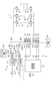
- FIG. 1 is a circuit diagram showing a configuration of a two-level inverter that is a first embodiment of the present invention
- FIG. It is a figure which illustrates the mode of switching on / off of the switching element at the time of normal in the embodiment. It is a figure which shows the electric potential difference between the output terminals in each mode at the normal time in the same embodiment. It is a figure which illustrates the aspect of switching of ON / OFF of a switching element when only one torque-off instruction
- FIG. 1 is a circuit diagram showing a configuration of a two-level inverter according to a first embodiment of the present invention. As shown in FIG. 1, the two-level inverter includes a main circuit 1, a control device 2, and a safety control device 3.
- the main circuit 1 has U-arm, V-phase, and W-phase upper arm switching elements 11 to 13 and U-phase, V-phase, and W-phase lower arm switching elements 14 to 16.
- Each switching element is composed of a semiconductor switching element such as an insulated gate bipolar transistor (IGBT) or a MOSFET and a free wheel diode connected in reverse parallel to the semiconductor switching element.
- the collectors of the IGBTs of the upper arm switching elements 11 to 13 are connected to the positive voltage terminal P, and the emitters of the IGBTs of the lower arm switching elements 14 to 16 are connected to the negative voltage terminal N.
- the emitters of the IGBTs of the upper arm switching elements 11 to 13 are connected to the collectors of the IGBTs of the lower arm switching elements 14 to 16, respectively, and nodes N1, N2 are connected to these emitters and collectors.
- N3 are a U-phase output terminal U, a V-phase output terminal V, and a W-phase output terminal W.
- a converter (not shown) is provided at the front stage of the two-level inverter, and this converter outputs a DC voltage between the positive voltage terminal P and the negative voltage terminal N.
- the two-level inverter converts the DC voltage between the positive voltage terminal P and the negative voltage terminal N into a three-phase AC voltage, and from the U-phase output terminal U, the V-phase output terminal V, and the W-phase output terminal W to an electric motor (illustrated) Are output to the U-phase winding, V-phase winding, and W-phase winding.
- the electric motor is, for example, a synchronous motor.
- the control device 2 includes a control signal generation circuit 21 and photocouplers PC1 to PC6.
- the control signal generation circuit 21 is used to switch on / off the control signals C1 to C3 for switching the upper arm switching elements 11 to 13 on the main circuit 1 and on / off the lower arm switching elements 14 to 16. This circuit generates control signals C4 to C6.
- the control signals C1 to C6 generated by the control signal generation circuit 21 pass through the photocouplers PC1 to PC6, respectively, and become gate signals G1 to G6, which are supplied to the gates of the IGBTs of the switching elements 11 to 16, respectively. .
- Each of the photocouplers PC1 to PC6 includes a photodiode and a phototransistor.
- Control signals C1 to C6 are supplied to the cathodes of the photodiodes of the photocouplers PC1 to PC6, respectively.
- the anodes of the photodiodes of the photocouplers PC3 and PC6 are connected to the photocoupler power supply P5, respectively.
- gate signals G1 to G6 for the IGBTs of the switching elements 11 to 16 are generated based on the collector-emitter voltages of the phototransistors of the photocouplers PC1 to PC6.
- the safety control device 3 includes torque-off processing circuits 311 and 312, delay circuits 321 and 322, and transistors 331 and 332.
- the transistor 331 has a collector connected to the photocoupler power supply P5s and an emitter connected to the anodes of the photodiodes of the photocouplers PC1 and PC2 via the feeder line 361.
- the transistor 332 has a collector connected to the photocoupler power supply P5s and an emitter connected to the anodes of the photodiodes of the photocouplers PC4 and PC5 via the feeder line 362.
- the torque-off processing circuit 311 supplies an H level signal to the base of the transistor 331 via the delay circuit 321 during normal operation. Further, the torque-off processing circuit 312 supplies an H level signal to the base of the transistor 332 via the delay circuit 322 in a normal state. Accordingly, in the normal state, the transistors 331 and 332 are turned on, and the power from the photocoupler power supply P5s passes through the transistors 331 and 332, and the photodiodes of the photocouplers PC1 and PC2 and the photocouplers PC4 and PC5. Each is supplied to a photodiode.
- the torque-off processing circuit 311 receives the torque-off command TOF1
- the torque-off processing circuit 312 receives the torque-off command TOF2.
- the torque-off commands TOF1 and TOF2 are commands that are generated based on a common event such as an operation of pressing a stop button by a user of the motor.
- the torque-off commands TOF1 and TOF2 do not necessarily need to be commands based on a common event, and the torque-off commands TOF1 and TOF2 may be generated based on different commands of different types and generations.
- the torque-off processing circuit 311 switches the signal given to the base of the transistor 331 via the delay circuit 321 from the H level to the L level. Therefore, the transistor 331 is turned off at the timing when the delay time of the delay circuit 321 has elapsed after the torque-off command TOF1 is input to the torque-off processing circuit 311 and the supply of power to the photodiodes of the photocouplers PC1 and PC2 is cut off. .
- the torque-off processing circuit 312 switches the signal given to the base of the transistor 332 via the delay circuit 322 from the H level to the L level. Accordingly, the transistor 332 is turned off at the timing when the delay time of the delay circuit 322 has elapsed after the torque-off command TOF2 is input to the torque-off processing circuit 312, and power supply to the photodiodes of the photocouplers PC4 and PC5 is cut off. .
- the torque-off processing circuit 311 takes in the potential of the node N4 to which the emitter of the transistor 331 is connected as the monitoring signal MON1, and determines whether the transistor 331 is on / off based on the monitoring signal MON1.
- the torque-off processing circuit 312 takes in the potential of the node N5 to which the emitter of the transistor 332 is connected as the monitoring signal MON2, and determines whether the transistor 332 is on / off based on the monitoring signal MON2.
- the above is the configuration of the two-level inverter.
- the control signal generation circuit 21 When the control command CMD is given to the control signal generation circuit 21, the control signal generation circuit 21 generates control signals C1 to C6.
- the control signals C1 to C6 pass through the photocouplers PC1 to PC6, become gate signals G1 to G6, and are supplied to the gates of the IGBTs of the switching elements 11 to 16, respectively.
- the switching elements 11 to 16 are switched on / off, and a three-phase AC voltage is output from the output terminals U, V and W to the motor.
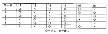
- FIG. 2 is a diagram illustrating an example of switching on / off of the switching elements 11 to 16.
- the on / off states of the switching elements 11 to 16 during normal operation of the two-level inverter include modes 1 to 6 shown in FIG.
- FIG. 3 is a diagram showing a potential difference between output terminals in each mode. In the example shown in FIG. 3, a DC voltage + E is applied between the positive voltage terminal P and the negative voltage terminal N.
- V (U ⁇ V) is the potential difference of the U-phase output terminal U with respect to the V-phase output terminal V
- V (V ⁇ W) is the potential difference of the V-phase output terminal V with respect to the W-phase output terminal W
- V ( W ⁇ U) indicates a potential difference of the W-phase output terminal W with respect to the U-phase output terminal U.
- the two-level inverter outputs three types of voltages + E, 0, and ⁇ E to the electric motor as shown in FIG. 3 by switching on / off of the switching elements 11 to 16.
- the upper arm switching elements 11 and 13 and the lower arm switching element 15 are turned on, and the upper arm switching element 12 and the lower arm switching elements 14 and 16 are turned off. Therefore, the W-phase output terminal W and the U-phase output terminal U are equipotential, and a current flows from the U-phase output terminal U and the W-phase output terminal W to the V-phase output terminal V through the motor.
- V (U ⁇ V) is + E
- V (V ⁇ W) is ⁇ E
- V (W ⁇ U) 0.
- modes 1 to 6 are changed by switching on / off of switching elements 11 to 16 with the passage of time, and V (U ⁇ V), V (V ⁇ W), and V ( WU) changes.
- V (U ⁇ V), V (V ⁇ W), and V ( WU) changes.
- control signal generation circuit 21 controls the on-time of the switching elements 11 to 16 so that the current flowing through the motor gradually decreases. As a result, the torque of the electric motor gradually decreases, the rotational speed of the electric motor decreases, and finally the electric motor stops.
- Torque-off processing circuits 311 and 312 switch output signals for delay circuits 321 and 322 from H level to L level when torque-off commands TOF1 and TOF2 are applied.
- the transistors 331 and 332 are turned off at the timing when the delay times of the delay circuits 321 and 322 have elapsed after the torque-off commands TOF1 and TOF2 are input to the torque-off processing circuits 311 and 312 respectively, and the photocouplers PC1, PC2, and PC4 And the power supply to the PC 5 is cut off.
- the torque-off processing circuits 311 and 312 receive the monitoring signals MON1 and MON2, respectively, and monitor the supply status of the power of the photocoupler power supply P5s to the photocouplers PC1, PC2, PC4, and PC5. Then, when the torque-off processing circuits 311 and 312 confirm that the supply of power to the photocouplers PC1, PC2, PC4, and PC5 has been cut off, a signal indicating that torque-off has been performed is sent to the host device of the safety control device 3 (Not shown).
- FIG. 4 is a diagram illustrating an on / off switching mode of the switching elements 11 to 16 in this case.
- modes 1, 5, and 6 no current flows through the windings of the motor, so that no magnetic field that rotates the rotor once is generated in the motor. For this reason, torque sufficient to rotate the electric motor is not generated.
- modes 2 to 4 since a current flows through the winding of the motor, the motor torque is not completely turned off.
- the torque is not completely turned off depending on the mode. This is the same even when the transistor 331 is on and the transistor 332 is off. Therefore, in this embodiment, the transistors 331 and 332 are turned off in response to the torque-off commands TOF1 and TOF2.
- FIG. 5 is a diagram illustrating an on / off switching mode of the switching elements 11 to 16 when the torque-off commands TOF1 and TOF2 are generated.
- the upper arm switching elements 11 and 12 and the lower arm switching elements 14 and 15 are turned off, and the upper arm switching element 13 and the lower arm switching element 16 are switched on / off. No electric current flows through the motor in all the five modes. Therefore, the torque of the electric motor is completely turned off.
- the delay time of the delay circuits 321 and 322 is set to a time longer than the time required for the inverter stop control by the control signal generating circuit 21, and the torque off is longer than the time required for the inverter stop control by the control signal generating circuit 21.
- the inverter stop control by the processing circuits 311 and 312 is delayed.
- the control signal generation circuit 21 performs the stop control of the two-level inverter. After that, the torque off processing circuits 311 and 312 perform stop control of the two-level inverter.
- the reason why the two types of stop control are advanced in parallel with a time difference as described above is as follows. First, if only the control signal generation circuit 21 is configured to perform the stop control of the two-level inverter, the stop control of the two-level inverter may not be normally performed when any operation abnormality occurs in the control signal generation circuit 21. There is sex. On the other hand, when only the torque-off processing circuits 311 and 312 perform the stop control of the two-level inverter, the following problem occurs. That is, when the torque-off processing circuits 311 and 312 cut off the power supply to the photocouplers PC1, PC2, PC4, and PC5, the IGBTs of the switching elements 11, 12, 14, and 15 are turned off while the motor is rotating.
- the torque-off processing circuits 311 and 312 are provided in preparation for the case where the stop control of the two-level inverter by the control signal generation circuit 21 ends in a malfunction. The above is the operation of the two-level inverter when the torque-off commands TOF1 and TOF2 are given.
- the three-phase upper arm switching elements 11, 12, and 13 are forcibly turned off in response to the torque-off command TOF1
- the three-phase lower arm switching elements 14, 15, and 16 are in response to the torque-off command TOF2.
- the two-phase upper arm switching elements 11 and 12 are forcibly turned OFF in response to the torque-off command TOF1
- the two-phase lower arm switching elements 14 and 15 are forcibly turned in response to the torque-off command TOF2.
- the supply of power to the photocouplers PC1 and PC2 for two phases is cut off in response to the torque-off command TOF1
- the supply of power to the photocouplers PC4 and PC5 for two phases is cut off in response to the torque-off command TOF2. It suffices if there is a wiring for two phases for that purpose (specifically, the connection destination of the power supply lines 361 and 362 may be two phases).
- the number of wires can be reduced without impairing the reliability with respect to complete torque-off of the electric motor as compared with the conventional two-level inverter. Therefore, it is possible to reduce the manufacturing cost of the two-level inverter and simplify the manufacturing work.
- the upper arm switching element and the lower arm switching element corresponding to the U phase and the V phase except for the W phase are forcibly turned off in response to the torque off commands TOF1 and TOF2.
- the upper arm switching element and the lower arm switching element corresponding to the V phase and the W phase may be forcibly turned off, or the upper arm switching element and the lower arm corresponding to the U phase and the W phase, excluding the V phase.
- the switching element may be forcibly turned off.
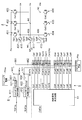
- FIG. 6 is a circuit diagram showing a configuration of a three-level inverter according to the second embodiment of the present invention.
- the main circuit 4 includes U-phase, V-phase, and W-phase upper arm switching elements 401, 402, and 403 and U-phase, V-phase, and W-phase lower arm switching, as in the first embodiment.
- These switching elements 401 to 406 are composed of IGBTs and freewheeling diodes connected in antiparallel with each other.
- the collectors of the IGBTs of the upper arm switching elements 401 to 403 are connected to the positive voltage terminal Pa, and the emitters of the IGBTs of the lower arm switching elements 404 to 406 are connected to the negative voltage terminal Na.
- the emitters of the IGBTs of the upper arm switching elements 401 to 403 are connected to the collectors of the IGBTs of the lower arm switching elements 404 to 406, respectively.
- the node N9 is a U-phase output terminal Ua, a V-phase output terminal Va, and a W-phase output terminal Wa.
- the U-phase, V-phase, and W-phase first reverse blocking switching elements 407 to 409 are each formed of an IGBT, each emitter is connected to a neutral point NP, and each collector is connected to nodes N7, N8. And N9, respectively.
- the U-phase, V-phase, and W-phase second reverse blocking switching elements 410 to 412 are each formed of an IGBT, each collector is connected to a neutral point NP, and each emitter is connected to a node N7. , N8 and N9, respectively.
- the neutral point NP is fixed to an intermediate voltage (grounded in the illustrated example) between the positive voltage terminal Pa and the negative voltage terminal Na.
- the control device 5 includes a control signal generation circuit 51 and photocouplers PCa1 to PCa12.
- the control signal generation circuit 51 controls the control signals Ca1 to Ca3 for switching on / off the upper arm switching elements 401 to 403 and the on / off switching of the lower arm switching elements 404 to 406.
- Control signals Ca4 to Ca6 control signals Ca7 to Ca9 for switching on / off of the first reverse blocking switching elements 407 to 409, and on / off switching of the second reverse blocking switching elements 410 to 412
- control signals Ca1 to Ca12 generated by the control signal generating circuit 51 pass through the photocouplers PCa1 to PCa12, respectively, and are supplied to the gates of the IGBTs of the switching elements 401 to 412 as the gate signals Ga1 to Ga12. .
- Control signals Ca1 to Ca12 are supplied to the cathodes of the photodiodes of the photocouplers PCa1 to PCa12, respectively.
- the anodes of the photodiodes of the photocouplers PCa3, PCa6, PCa9, and PCa12 are connected to the photocoupler power supply P5a.
- gate signals Ga1 to Ga12 for the IGBTs of the switching elements 401 to 412 are generated based on the collector-emitter voltages of the phototransistors of the photocouplers PCa1 to PCa12.
- the collectors of the transistors 631 and 632 are connected to the photocoupler power supply P5sa.
- the emitter of the transistor 631 is connected to the anodes of the photodiodes of the photocouplers PCa1, PCa2, PCa10, and PCa11 through the feeder line 661.
- the emitter of the transistor 632 is connected to the anodes of the photodiodes of the phototransistors PCa4, PCa5, PCa7, and PCa8 through the feeder line 662, respectively.
- Torque-off processing circuits 611 and 612 are connected to the bases of transistors 631 and 632 via delay circuits 621 and 622, respectively. The above is the configuration of the three-level inverter.
- the transistors 631 and 632 are turned on, and the power of the photocoupler power supply P5sa is supplied to the photocouplers PCa1, PCa2, PCa10, PCa11, PCa4, PCa5, PCa7 and the transistors 631 and 632, respectively. Each is supplied to PCa8.
- the control signal CMDa is supplied to the control signal generation circuit 51
- the control signal generation circuit 51 generates the control signals Ca1 to Ca12.
- the control signals Ca1 to Ca12 pass through the photocouplers PCa1 to PCa12, respectively, become gate signals Ga1 to Ga12, and are supplied to the gates of the switching elements 401 to 412, respectively.
- each of switching elements 401 to 412 is switched on / off, and a three-phase AC voltage is output from output terminals U, V and W to the motor.
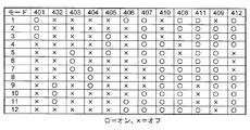
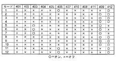
- FIG. 7 is a diagram illustrating an example of switching on / off of the switching elements 401 to 412.
- the on / off states of the switching elements 401 to 412 during the normal operation of the three-level inverter include modes 1 to 12 shown in FIG.
- FIG. 8 is a diagram showing the potential difference between the output terminals in each mode.
- a DC voltage + E is applied between the positive voltage terminal Pa and the neutral point NP and between the neutral point NP and the negative voltage terminal Na.
- five types of voltages of + 2E, + E, 0, ⁇ E, and ⁇ 2E are output to the motor as shown in FIG.
- the upper arm switching element 401, the lower arm switching element 406, and the reverse blocking switching elements 407, 408, 411 and 412 are turned on, and the upper arm switching elements 402 and 403 and the lower arm Switching elements 404 and 405 and reverse blocking switching elements 409 and 410 are off. Therefore, current flows from the U-phase output terminal Ua to the V-phase output terminal Va and the W-phase output terminal Wa via the electric motor.
- V (U ⁇ V) is + E
- V (V ⁇ W) is + E
- V (W ⁇ U) is ⁇ 2E.
- modes 1 to 12 are changed by switching on / off of switching elements 401 to 412 over time, and V (U ⁇ V), V (V ⁇ W) and V ( WU) changes.
- the three-level inverter supplies such an AC voltage to the electric motor through the U-phase output terminal Ua, the V-phase output terminal Va, and the W-phase output terminal Wa, so that a rotating magnetic field is generated in the electric motor, and the rotor of the electric motor rotates.
- the above is the normal operation of the three-level inverter.
- control signal generation circuit 51 controls the on-time of the switching elements 401 to 412 so that the current flowing from the three-level inverter to the motor gradually decreases. As a result, the torque of the electric motor gradually decreases, the rotational speed of the electric motor decreases, and finally the electric motor stops.
- Torff-off processing circuits 611 and 612 switch output signals for delay circuits 621 and 622 from the H level to the L level when torque-off commands TOF1a and TOF2a are applied.
- the transistors 631 and 632 are turned off at the timing when the delay times of the delay circuits 621 and 622 have elapsed since the torque-off commands TOF1a and TOF2a were input to the torque-off processing circuits 611 and 612, and the photocouplers PCa1, PCa2, PCa10, Supply of power to PCa11, PCa4, PCa5, PCa7, and PCa8 is cut off.
- the delay times of the delay circuits 621 and 622 are set to be longer than the time taken for the inverter stop control by the control signal generation circuit 51.
- the torque-off processing circuits 611 and 612 receive the monitoring signals MON1a and MON2a, respectively, and monitor the power supply status to the photocouplers PCa1, PCa2, PCa10, PCa11, PCa4, PCa5, PCa7, and PCa8. Then, when the torque-off processing circuits 611 and 612 confirm that the supply of power to the photocouplers PCa1, PCa2, PCa10, PCa11, PCa4, PCa5, PCa7, and PCa8 is cut off, a signal indicating that torque-off has been performed. Is transmitted to a host device (not shown) of the safety control device 6.
- the switching elements 401, 402, 404, 405, 407, 408, 409, and 410 receive control signals Ca1 to Regardless of the state of Ca12, only the switching elements 403, 406, 411, and 412 are switched off and switched on / off in the main circuit 4. As a result, the torque of the electric motor connected to the main circuit 4 becomes zero.
- FIG. 9 is a diagram exemplifying a mode of switching on / off of the switching elements 401 to 412 when the torque-off commands TOF1a and TOF2a are generated.
- the upper arm switching elements 401 and 402 the second reverse blocking switching elements 410 and 411, the lower arm switching elements 404 and 405, and the first reverse blocking switching elements 407 and 408 are provided. Turns off.
- the upper arm switching element 403, the lower arm switching element 406, and the reverse blocking switching elements 409 and 412 are switched on / off, but no current flows through the motor in all modes of FIG. Therefore, the torque of the electric motor is completely turned off.
- the control signal generation circuit 51 performs stop control of the three-level inverter. Thereafter, the torque-off processing circuits 611 and 612 perform stop control of the three-level inverter.
- the reason why the two types of stop control are advanced in parallel with a time difference is the same as in the first embodiment.
- the above is the operation of the three-level inverter when the torque-off commands TOF1a and TOF2a are given. Also in this embodiment, the same effect as the first embodiment can be obtained.
- the upper arm switching element, the lower arm switching element, and the reverse blocking switching element corresponding to the U phase and the V phase, excluding the W phase are forced according to the first and second torque-off commands.
- the upper arm switching element, the lower arm switching element, and the reverse blocking switching element corresponding to the V phase and the W phase except for the U phase may be forcibly turned off, or the V phase may be excluded.
- the upper arm switching element, the lower arm switching element, and the reverse blocking switching element corresponding to the U phase and the W phase may be forcibly turned off.
- the first and second embodiments of the present invention have been described above, other embodiments are conceivable for the present invention.
- the control signal generating circuit 21, the photocoupler, and the switching elements of the main circuit 4 are stored in separate housings for each of the U phase, the V phase, and the W phase.
- the switching elements corresponding to the W phase are not forcibly turned off in response to the torque-off command, the switching elements of the control signal generating circuit 21, the photocoupler, and the main circuit 4 corresponding to the W phase are stored.
- the number of wires in the housing can be reduced and the housing can be downsized.
Abstract
Description
図1は、この発明の第1実施形態である2レベルインバータの構成を示す回路図である。図1に示すように、この2レベルインバータは、主回路1と、制御装置2と、安全制御装置3とにより構成されている。
以上が、2レベルインバータの構成である。
以上が、2レベルインバータの通常時の動作である。
以上が、トルクオフ指令TОF1およびTОF2が与えられた時の2レベルインバータの動作である。
図6は、この発明の第2実施形態である3レベルインバータの構成を示す回路図である。本実施形態において、主回路4は、上記第1実施形態と同様、U相、V相およびW相の上アームスイッチング素子401、402および403と、U相、V相およびW相の下アームスイッチング素子404、405および406とを有する。これらのスイッチング素子401~406は、互いに逆並列接続されたIGBTとフリーホイールダイオードから構成されている。上アームスイッチング素子401~403の各IGBTのコレクタは、正電圧端子Paに接続され、下アームスイッチング素子404~406の各IGBTのエミッタは、負電圧端子Naに接続される。そして、上アームスイッチング素子401~403の各IGBTのエミッタは、下アームスイッチング素子404~406の各IGBTのコレクタと各々接続されており、これらのエミッタとコレクタが互いに接続されたノードN7、ノードN8およびノードN9はU相出力端子Ua、V相出力端子VaおよびW相出力端子Waとなっている。
以上が、3レベルインバータの構成である。
以上が、3レベルインバータの通常時の動作である。
以上が、トルクオフ指令TОF1aおよびTОF2aが与えられた時の3レベルインバータの動作である。本実施形態においても上記第1実施形態と同様な効果が得られる。
Claims (4)
- 正電圧端子に接続された3相の上アームスイッチング素子と負電圧端子に接続された3相の下アームスイッチング素子を有し、前記3相の上アームスイッチング素子と前記3相の下アームスイッチング素子の各相の接続点を各相の出力端子とする主回路と、前記3相の上アームスイッチング素子および前記3相の下アームスイッチング素子をオン/オフさせるパルスを出力することにより前記主回路の各相の出力端子から交流電圧を電動機に各々出力させる制御装置とを有するインバータの安全制御装置において、
第1のトルクオフ指令に応じて、前記制御装置からのパルスの発生状態に拘わらず、前記3相の上アームスイッチング素子のうち2相の上アームスイッチング素子をオフとする第1のトルクオフ回路と、
第2のトルクオフ指令に応じて、前記制御装置からのパルスの発生状態に拘わらず、前記2相の上アームスイッチング素子と同一の2相の下アームスイッチング素子をオフとする第2のトルクオフ回路と
を具備することを特徴とする安全制御装置。 - 前記第1のトルクオフ回路は、前記第1のトルクオフ指令の発生時点から所定時間遅れて前記2相の上アームスイッチング素子をオフとし、
前記第2のトルクオフ回路は、前記第2のトルクオフ指令の発生時点から所定時間遅れて前記2相の下アームスイッチング素子をオフとすることを特徴とする請求項1に記載の安全制御装置。 - 前記主回路は、前記正電圧端子および前記負電圧端子の中間の電圧を発生する中性点に各々のエミッタが接続され、前記主回路の3相の出力端子に各々のコレクタが接続された3相の第1の逆阻止型スイッチング素子と、前記中性点に各々のコレクタが接続され、前記主回路の3相の出力端子に各々のエミッタが接続された3相の第2の逆阻止型スイッチング素子とを具備し、
前記第1のトルクオフ回路は、前記第1のトルクオフ指令に応じて、前記制御装置からのパルスの発生状態に拘わらず、前記2相の上アームスイッチング素子に対応した前記第2の逆阻止型スイッチング素子をオフとし、
前記第2のトルクオフ回路は、前記第2のトルクオフ指令に応じて、前記制御装置からのパルスの発生状態に拘わらず、前記2相の上アームスイッチング素子に対応した前記第1の逆阻止型スイッチング素子をオフとすることを特徴とする請求項1に記載の電動機の安全制御装置。 - 前記第1のトルクオフ回路は、前記第1のトルクオフ指令の発生時点から所定時間遅れて前記2相の上アームスイッチング素子および前記2相の上アームスイッチング素子に対応した第2の逆阻止型スイッチング素子をオフとし、
前記第2のトルクオフ回路は、前記第2のトルクオフ指令の発生時点から所定時間遅れて前記2相の下アームスイッチング素子および前記2相の下アームスイッチング素子に対応した第1の逆阻止型スイッチング素子をオフとすることを特徴とする請求項3に記載の安全制御装置。
Priority Applications (3)
| Application Number | Priority Date | Filing Date | Title |
|---|---|---|---|
| CN201580001837.0A CN105531921B (zh) | 2014-04-03 | 2015-03-31 | 安全控制装置 |
| JP2016511933A JP6197950B2 (ja) | 2014-04-03 | 2015-03-31 | 安全制御装置 |
| EP15772913.8A EP3128669B1 (en) | 2014-04-03 | 2015-03-31 | Safety control device |
Applications Claiming Priority (2)
| Application Number | Priority Date | Filing Date | Title |
|---|---|---|---|
| JP2014077049 | 2014-04-03 | ||
| JP2014-077049 | 2014-04-03 |
Publications (1)
| Publication Number | Publication Date |
|---|---|
| WO2015152245A1 true WO2015152245A1 (ja) | 2015-10-08 |
Family
ID=54240565
Family Applications (1)
| Application Number | Title | Priority Date | Filing Date |
|---|---|---|---|
| PCT/JP2015/060136 WO2015152245A1 (ja) | 2014-04-03 | 2015-03-31 | 安全制御装置 |
Country Status (4)
| Country | Link |
|---|---|
| EP (1) | EP3128669B1 (ja) |
| JP (1) | JP6197950B2 (ja) |
| CN (1) | CN105531921B (ja) |
| WO (1) | WO2015152245A1 (ja) |
Citations (5)
| Publication number | Priority date | Publication date | Assignee | Title |
|---|---|---|---|---|
| JP2009081951A (ja) * | 2007-09-26 | 2009-04-16 | Jtekt Corp | モータ制御装置及び電動パワーステアリング装置 |
| JP2010252567A (ja) * | 2009-04-17 | 2010-11-04 | Daikin Ind Ltd | 電源回路 |
| JP2010284051A (ja) * | 2009-06-08 | 2010-12-16 | Fuji Electric Systems Co Ltd | インバータ装置 |
| JP2013085325A (ja) * | 2011-10-06 | 2013-05-09 | Fuji Electric Co Ltd | 3レベル電力変換回路システム |
| WO2014199732A1 (ja) * | 2013-06-14 | 2014-12-18 | 富士電機株式会社 | マルチレベルインバータ |
Family Cites Families (5)
| Publication number | Priority date | Publication date | Assignee | Title |
|---|---|---|---|---|
| GB9300734D0 (en) * | 1993-01-14 | 1993-03-03 | Switched Reluctance Drives Ltd | High voltage power converters for switched reluctance motors |
| JP3074234B2 (ja) * | 1993-11-09 | 2000-08-07 | 株式会社日立製作所 | 直列多重インバータ装置の制御方法 |
| JP5157292B2 (ja) * | 2007-07-18 | 2013-03-06 | 富士電機株式会社 | 3レベルインバータの制御方式 |
| JP4968698B2 (ja) * | 2008-12-26 | 2012-07-04 | 本田技研工業株式会社 | 電動機の制御装置 |
| US8988836B2 (en) * | 2009-04-17 | 2015-03-24 | Daikin Industries, Ltd. | Power circuit, and computer-readable recording medium storing a control program for power circuits |
-
2015
- 2015-03-31 CN CN201580001837.0A patent/CN105531921B/zh active Active
- 2015-03-31 EP EP15772913.8A patent/EP3128669B1/en active Active
- 2015-03-31 JP JP2016511933A patent/JP6197950B2/ja active Active
- 2015-03-31 WO PCT/JP2015/060136 patent/WO2015152245A1/ja active Application Filing
Patent Citations (5)
| Publication number | Priority date | Publication date | Assignee | Title |
|---|---|---|---|---|
| JP2009081951A (ja) * | 2007-09-26 | 2009-04-16 | Jtekt Corp | モータ制御装置及び電動パワーステアリング装置 |
| JP2010252567A (ja) * | 2009-04-17 | 2010-11-04 | Daikin Ind Ltd | 電源回路 |
| JP2010284051A (ja) * | 2009-06-08 | 2010-12-16 | Fuji Electric Systems Co Ltd | インバータ装置 |
| JP2013085325A (ja) * | 2011-10-06 | 2013-05-09 | Fuji Electric Co Ltd | 3レベル電力変換回路システム |
| WO2014199732A1 (ja) * | 2013-06-14 | 2014-12-18 | 富士電機株式会社 | マルチレベルインバータ |
Also Published As
| Publication number | Publication date |
|---|---|
| JPWO2015152245A1 (ja) | 2017-04-13 |
| CN105531921B (zh) | 2018-08-28 |
| CN105531921A (zh) | 2016-04-27 |
| EP3128669B1 (en) | 2020-09-09 |
| EP3128669A4 (en) | 2017-11-01 |
| JP6197950B2 (ja) | 2017-09-20 |
| EP3128669A1 (en) | 2017-02-08 |
Similar Documents
| Publication | Publication Date | Title |
|---|---|---|
| JP4662316B2 (ja) | 交流電動機の巻線切替装置およびその巻線切替システム | |
| JP5433608B2 (ja) | 電力変換装置 | |
| WO2013051202A1 (ja) | 3レベル電力変換回路システム | |
| JP2015012621A (ja) | マルチレベル電力変換回路 | |
| JP2014533487A (ja) | Hブリッジに基づく電力変換器 | |
| US9712044B2 (en) | Power converter | |
| JP2012231599A (ja) | 直列多重電力変換装置 | |
| JP2015159684A (ja) | 回転電機制御装置 | |
| JP2015032984A (ja) | 半導体素子の駆動装置およびそれを用いた電力変換装置 | |
| JP2009296858A (ja) | 電力変換装置 | |
| EP3010137B1 (en) | Multilevel inverter | |
| JP2015527858A (ja) | モーション及びコントロールシステム | |
| JP6197950B2 (ja) | 安全制御装置 | |
| CN111095766B (zh) | 驱动器组中的中间电路耦连 | |
| WO2017046964A1 (ja) | インバータ装置及びインバータ装置の制御方法 | |
| JP7373424B2 (ja) | 電力変換装置 | |
| JP2016127677A (ja) | 電力変換装置 | |
| WO2023286627A1 (ja) | 電力変換装置および電力変換方法 | |
| JP6376049B2 (ja) | 回転機の制御装置 | |
| JP7460508B2 (ja) | 電力変換装置 | |
| JP7109631B1 (ja) | 電力変換装置 | |
| JP6099004B1 (ja) | インバータ装置及びインバータ装置の製造方法 | |
| JP2011139590A (ja) | 電流型インバータ装置 | |
| KR102453339B1 (ko) | 고장 회피 회로를 가지는 멀티레벨 인버터 | |
| JP2000023466A (ja) | インバータ装置 |
Legal Events
| Date | Code | Title | Description |
|---|---|---|---|
| WWE | Wipo information: entry into national phase |
Ref document number: 201580001837.0 Country of ref document: CN |
|
| 121 | Ep: the epo has been informed by wipo that ep was designated in this application |
Ref document number: 15772913 Country of ref document: EP Kind code of ref document: A1 |
|
| REEP | Request for entry into the european phase |
Ref document number: 2015772913 Country of ref document: EP |
|
| ENP | Entry into the national phase |
Ref document number: 2016511933 Country of ref document: JP Kind code of ref document: A |
|
| NENP | Non-entry into the national phase |
Ref country code: DE |