WO2015152002A1 - インバータ制御装置 - Google Patents
インバータ制御装置 Download PDFInfo
- Publication number
- WO2015152002A1 WO2015152002A1 PCT/JP2015/059406 JP2015059406W WO2015152002A1 WO 2015152002 A1 WO2015152002 A1 WO 2015152002A1 JP 2015059406 W JP2015059406 W JP 2015059406W WO 2015152002 A1 WO2015152002 A1 WO 2015152002A1
- Authority
- WO
- WIPO (PCT)
- Prior art keywords
- phase
- control
- inverter
- current
- arm
- Prior art date
- Legal status (The legal status is an assumption and is not a legal conclusion. Google has not performed a legal analysis and makes no representation as to the accuracy of the status listed.)
- Ceased
Links
Images



Classifications
-
- H—ELECTRICITY
- H02—GENERATION; CONVERSION OR DISTRIBUTION OF ELECTRIC POWER
- H02P—CONTROL OR REGULATION OF ELECTRIC MOTORS, ELECTRIC GENERATORS OR DYNAMO-ELECTRIC CONVERTERS; CONTROLLING TRANSFORMERS, REACTORS OR CHOKE COILS
- H02P29/00—Arrangements for regulating or controlling electric motors, appropriate for both AC and DC motors
- H02P29/02—Providing protection against overload without automatic interruption of supply
- H02P29/024—Detecting a fault condition, e.g. short circuit, locked rotor, open circuit or loss of load
-
- B—PERFORMING OPERATIONS; TRANSPORTING
- B60—VEHICLES IN GENERAL
- B60L—PROPULSION OF ELECTRICALLY-PROPELLED VEHICLES; SUPPLYING ELECTRIC POWER FOR AUXILIARY EQUIPMENT OF ELECTRICALLY-PROPELLED VEHICLES; ELECTRODYNAMIC BRAKE SYSTEMS FOR VEHICLES IN GENERAL; MAGNETIC SUSPENSION OR LEVITATION FOR VEHICLES; MONITORING OPERATING VARIABLES OF ELECTRICALLY-PROPELLED VEHICLES; ELECTRIC SAFETY DEVICES FOR ELECTRICALLY-PROPELLED VEHICLES
- B60L50/00—Electric propulsion with power supplied within the vehicle
- B60L50/50—Electric propulsion with power supplied within the vehicle using propulsion power supplied by batteries or fuel cells
- B60L50/51—Electric propulsion with power supplied within the vehicle using propulsion power supplied by batteries or fuel cells characterised by AC-motors
-
- H—ELECTRICITY
- H02—GENERATION; CONVERSION OR DISTRIBUTION OF ELECTRIC POWER
- H02M—APPARATUS FOR CONVERSION BETWEEN AC AND AC, BETWEEN AC AND DC, OR BETWEEN DC AND DC, AND FOR USE WITH MAINS OR SIMILAR POWER SUPPLY SYSTEMS; CONVERSION OF DC OR AC INPUT POWER INTO SURGE OUTPUT POWER; CONTROL OR REGULATION THEREOF
- H02M1/00—Details of apparatus for conversion
- H02M1/32—Means for protecting converters other than automatic disconnection
-
- H—ELECTRICITY
- H02—GENERATION; CONVERSION OR DISTRIBUTION OF ELECTRIC POWER
- H02M—APPARATUS FOR CONVERSION BETWEEN AC AND AC, BETWEEN AC AND DC, OR BETWEEN DC AND DC, AND FOR USE WITH MAINS OR SIMILAR POWER SUPPLY SYSTEMS; CONVERSION OF DC OR AC INPUT POWER INTO SURGE OUTPUT POWER; CONTROL OR REGULATION THEREOF
- H02M1/00—Details of apparatus for conversion
- H02M1/36—Means for starting or stopping converters
-
- H—ELECTRICITY
- H02—GENERATION; CONVERSION OR DISTRIBUTION OF ELECTRIC POWER
- H02M—APPARATUS FOR CONVERSION BETWEEN AC AND AC, BETWEEN AC AND DC, OR BETWEEN DC AND DC, AND FOR USE WITH MAINS OR SIMILAR POWER SUPPLY SYSTEMS; CONVERSION OF DC OR AC INPUT POWER INTO SURGE OUTPUT POWER; CONTROL OR REGULATION THEREOF
- H02M7/00—Conversion of AC power input into DC power output; Conversion of DC power input into AC power output
- H02M7/42—Conversion of DC power input into AC power output without possibility of reversal
- H02M7/44—Conversion of DC power input into AC power output without possibility of reversal by static converters
- H02M7/48—Conversion of DC power input into AC power output without possibility of reversal by static converters using discharge tubes with control electrode or semiconductor devices with control electrode
- H02M7/53—Conversion of DC power input into AC power output without possibility of reversal by static converters using discharge tubes with control electrode or semiconductor devices with control electrode using devices of a triode or transistor type requiring continuous application of a control signal
- H02M7/537—Conversion of DC power input into AC power output without possibility of reversal by static converters using discharge tubes with control electrode or semiconductor devices with control electrode using devices of a triode or transistor type requiring continuous application of a control signal using semiconductor devices only, e.g. single switched pulse inverters
- H02M7/5387—Conversion of DC power input into AC power output without possibility of reversal by static converters using discharge tubes with control electrode or semiconductor devices with control electrode using devices of a triode or transistor type requiring continuous application of a control signal using semiconductor devices only, e.g. single switched pulse inverters in a bridge configuration
-
- H—ELECTRICITY
- H02—GENERATION; CONVERSION OR DISTRIBUTION OF ELECTRIC POWER
- H02P—CONTROL OR REGULATION OF ELECTRIC MOTORS, ELECTRIC GENERATORS OR DYNAMO-ELECTRIC CONVERTERS; CONTROLLING TRANSFORMERS, REACTORS OR CHOKE COILS
- H02P27/00—Arrangements or methods for the control of AC motors characterised by the kind of supply voltage
- H02P27/04—Arrangements or methods for the control of AC motors characterised by the kind of supply voltage using variable-frequency supply voltage, e.g. inverter or converter supply voltage
- H02P27/06—Arrangements or methods for the control of AC motors characterised by the kind of supply voltage using variable-frequency supply voltage, e.g. inverter or converter supply voltage using DC to AC converters or inverters
-
- H—ELECTRICITY
- H02—GENERATION; CONVERSION OR DISTRIBUTION OF ELECTRIC POWER
- H02P—CONTROL OR REGULATION OF ELECTRIC MOTORS, ELECTRIC GENERATORS OR DYNAMO-ELECTRIC CONVERTERS; CONTROLLING TRANSFORMERS, REACTORS OR CHOKE COILS
- H02P29/00—Arrangements for regulating or controlling electric motors, appropriate for both AC and DC motors
- H02P29/02—Providing protection against overload without automatic interruption of supply
- H02P29/024—Detecting a fault condition, e.g. short circuit, locked rotor, open circuit or loss of load
- H02P29/0241—Detecting a fault condition, e.g. short circuit, locked rotor, open circuit or loss of load the fault being an overvoltage
-
- H—ELECTRICITY
- H02—GENERATION; CONVERSION OR DISTRIBUTION OF ELECTRIC POWER
- H02P—CONTROL OR REGULATION OF ELECTRIC MOTORS, ELECTRIC GENERATORS OR DYNAMO-ELECTRIC CONVERTERS; CONTROLLING TRANSFORMERS, REACTORS OR CHOKE COILS
- H02P6/00—Arrangements for controlling synchronous motors or other dynamo-electric motors using electronic commutation dependent on the rotor position; Electronic commutators therefor
- H02P6/14—Electronic commutators
-
- Y—GENERAL TAGGING OF NEW TECHNOLOGICAL DEVELOPMENTS; GENERAL TAGGING OF CROSS-SECTIONAL TECHNOLOGIES SPANNING OVER SEVERAL SECTIONS OF THE IPC; TECHNICAL SUBJECTS COVERED BY FORMER USPC CROSS-REFERENCE ART COLLECTIONS [XRACs] AND DIGESTS
- Y02—TECHNOLOGIES OR APPLICATIONS FOR MITIGATION OR ADAPTATION AGAINST CLIMATE CHANGE
- Y02T—CLIMATE CHANGE MITIGATION TECHNOLOGIES RELATED TO TRANSPORTATION
- Y02T10/00—Road transport of goods or passengers
- Y02T10/60—Other road transportation technologies with climate change mitigation effect
- Y02T10/70—Energy storage systems for electromobility, e.g. batteries
Definitions
- the present invention relates to a technique for driving and controlling an AC rotating electrical machine.
- a high-output AC rotating electric machine used for power of an electric vehicle or a hybrid vehicle is driven at a high voltage.
- the high voltage power supply mounted in such a motor vehicle is a direct current battery, it is converted into, for example, a three-phase alternating current by an inverter circuit using a switching element.
- the rotating electrical machine has not only a function as a motor that outputs power for driving a vehicle by electric energy but also a function as a generator that generates electric power by kinetic energy of a vehicle, an internal combustion engine, or the like.
- the electric power generated by the rotating electrical machine is regenerated and stored in the battery.
- a switchgear is provided between the battery and the rotating electric machine, more specifically between the battery and the inverter.
- the contactor is, for example, a system main relay (SMR) configured using a relay.
- SMR system main relay
- IG key ignition key
- the contact is closed and the IG key is off.
- the contact opens and becomes non-conductive. That is, the battery and the inverter (and the rotating electrical machine) are electrically connected when the SMR is closed, and the electrical connection between the battery and the inverter (and the rotating electrical machine) is disconnected when the SMR is open.
- the open / close state of the SMR is also controlled according to the state of the IG key.
- the SMR may be released due to a vehicle failure or a collision.
- Etc. when the power supply to the SMR is cut off, when an abnormality occurs in the SMR drive circuit, when the SMR mechanically fails due to vibration, shock, noise, etc., or when the circuit around the SMR is disconnected , Etc., the contact of the SMR may be opened, and the contactor may be opened.
- shutdown control for turning off all switching elements constituting the inverter may be performed.
- a smoothing capacitor DC link capacitor
- DC link voltage DC link voltage
- FWD free wheel diode
- the voltage between the terminals of the smoothing capacitor DC link voltage
- Increasing the capacity and withstand voltage of the smoothing capacitor in preparation for an increase in the DC link voltage leads to an increase in the size of the smoothing capacitor. Further, it is necessary to increase the breakdown voltage of the inverter. As a result, downsizing of the rotating electrical machine drive device is hindered, and the component cost, manufacturing cost, and product cost are also affected.
- active short control active short circuit control (active short circuit control (ASC control)
- ZVS control zero vector sequence control
- ASC control active short circuit control
- ZVS control zero vector sequence control
- Patent Document 1 discloses a control method in which all the upper switching elements of the inverter are turned off and any one or more of the lower switching elements are turned on. (Patent Document 1: FIG. 2, paragraphs 158, 159, 165, etc.).
- ASC control active short circuit control
- ZVS control zero vector sequence control
- a large current continues to flow until the electric power accumulated in the stator coil is consumed due to heat or the like. For this reason, a switching element and a stator coil may be consumed, and a lifetime may be reduced. Moreover, it becomes necessary to use a switching element corresponding to a large current, which may affect the component cost, manufacturing cost, and product cost.
- the characteristic configuration of the inverter control device in view of the above is Connected to a DC power source via a contactor and connected to an AC rotating electrical machine to perform power conversion between DC and three-phase AC, and an arm for one AC phase has an upper switching element and a lower switching element
- the inverter is configured with a rotating electrical machine driving device including an inverter configured by a series circuit with a switching element and a DC link capacitor that smoothes a DC link voltage that is a voltage on the DC side of the inverter as a control target.
- An inverter control device that controls switching of a switching element, Partial shutdown for controlling the switching element that is controlled to be on in the target arm that is one of the arms when the contactor is open during rotation of the rotating electrical machine. Execute control, After that, when both the currents of the two-phase arms different from the target arm become zero, the full shutdown is performed so that the switching elements that are controlled to be turned on in all the remaining arms are turned off. The point is to execute the control.
- the contactor connecting the inverter and the DC power supply when the contactor connecting the inverter and the DC power supply is in an open state, the increase in the DC link voltage of the inverter and the total amount of return current are suppressed, and the current flows to the rotating electrical machine.
- the current can be zero.
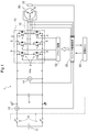
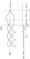
- Circuit block diagram schematically showing the system configuration of the rotating electrical machine drive device Waveform diagram schematically showing a control example when the contactor is open IGBT 1 control example in Phase 1 and equivalent circuit diagram showing current flow Example of IGBT control in Phase 2 and equivalent circuit diagram showing current flow Waveform diagram schematically showing another control example when the contactor is open IGBT 1 control example in Phase 1 and equivalent circuit diagram showing current flow Example of IGBT control in Phase 2 and equivalent circuit diagram showing current flow
- the inverter control device 20 controls the rotary electric machine drive device 1 including the inverter 10 and the DC link capacitor 4 and controls the rotary electric machine 80 via the rotary electric machine drive device 1.
- the inverter 10 is connected to the DC power source (11) via the contactor 9, and is connected to an AC rotating electrical machine 80 to connect between DC and multiphase AC (here, three-phase AC).
- the power conversion device performs power conversion, and an AC one-phase arm is configured by a series circuit of an upper-stage switching element and a lower-stage switching element.
- the DC link capacitor 4 smoothes the DC link voltage Vdc that is the voltage on the DC side of the inverter 10.
- the rotating electrical machine 80 to be driven by the rotating electrical machine drive device 1 and the inverter control device 20 is a rotating electrical machine that serves as a driving force source for a vehicle such as a hybrid vehicle or an electric vehicle.
- the rotating electrical machine 80 as a vehicle driving force source is a rotating electrical machine that operates by multiphase alternating current (here, three-phase alternating current), and can function as both an electric motor and a generator.
- a secondary battery such as a nickel metal hydride battery or a lithium ion battery is used as a power source for driving the rotating electrical machine 80, It is equipped with a DC power supply such as a double layer capacitor.
- a high voltage battery 11 DC power supply having a power supply voltage of 200 to 400 [V], for example, is provided as a high voltage and large capacity DC power supply for supplying power to the rotating electrical machine 80.
- an inverter 10 that performs power conversion between direct current and alternating current (here, three-phase alternating current) is provided between the high voltage battery 11 and the rotating electrical machine 80. Yes.
- the voltage between the positive power supply line P and the negative power supply line N on the DC side of the inverter 10 is hereinafter referred to as “DC link voltage Vdc”.
- the high voltage battery 11 can supply electric power to the rotating electrical machine 80 via the inverter 10 and can store electric power obtained by the rotating electrical machine 80 generating electric power.
- a smoothing capacitor for smoothing the voltage between the positive and negative electrodes (DC link voltage Vdc) on the DC side of the inverter 10 is provided.
- the DC link capacitor 4 stabilizes a DC voltage (DC link voltage Vdc) that fluctuates according to fluctuations in power consumption of the rotating electrical machine 80.
- a contactor 9 capable of disconnecting the electrical connection between the circuit from the DC link capacitor 4 to the rotating electrical machine 80 and the high voltage battery 11 is provided.
- the contactor 9 is a mechanical relay that opens and closes based on a command from a vehicle ECU (Electronic Control Unit) 90 that is one of the highest-level control devices of the vehicle.
- a system main relay SMR: System Main Relay
- IG key ignition key
- the contactor 9 closes the contact of the SMR and becomes conductive (connected)
- the contactor 9 The contact of is opened and becomes a non-conductive state (open state).
- the inverter 10 is interposed between the high voltage battery 11 and the rotating electrical machine 80 via the contactor 9, and when the contactor 9 is in the connected state, the high voltage battery 11 and the inverter 10 (and the rotating electrical machine 80) are electrically connected to each other.
- 9 is open, the electrical connection between the high voltage battery 11 and the inverter 10 (and the rotating electrical machine 80) is cut off.
- the inverter 10 converts the DC power having the DC link voltage Vdc into AC power of a plurality of phases (n is a natural number, n-phase, here, three phases) and supplies the AC power to the rotating electrical machine 80, and the AC generated by the rotating electrical machine 80 The power is converted to DC power and supplied to the DC power supply.
- the inverter 10 includes a plurality of switching elements.
- the switching elements include IGBT (Insulated Gate Bipolar Transistor), Power MOSFET (Metal Oxide Semiconductor Semiconductor Field Field Effect Transistor), SiC-MOSFET (Silicon Carbon-Metal Metal Oxide Semiconductor Semiconductor FET), SiC-SIT (SiC-Static InGaN Transistor). It is preferable to apply a power semiconductor element capable of operating at a high frequency such as a MOSFET (Gallium Nitride-MOSFET). As shown in FIG. 1, in this embodiment, IGBT3 is used as a switching element.
- an inverter 10 that converts power between direct current and multiphase alternating current (here, three-phase alternating current) has a number of arms corresponding to each of the multiple phases (here, three phases) as is well known. Consists of a circuit. That is, as shown in FIG. 1, two IGBTs 3 are provided between the DC positive side (positive power supply line P on the positive side of the DC power supply) and the DC negative side (negative power supply line N on the negative side of the DC power supply) of the inverter 10. Are connected in series to form one arm. In the case of three-phase alternating current, this series circuit (one arm) is connected in parallel with three lines (three phases). That is, a bridge circuit in which a set of series circuits (arms) corresponds to each of the stator coils 8 corresponding to the U phase, the V phase, and the W phase of the rotating electrical machine 80 is configured.
- the connection point with the IGBT 3 on the power supply line N side is the stator coil 8 (8u, 8v, 8w: FIG. 3 etc.) of the rotating electrical machine 80. Connected to each other).
- Each IGBT 3 is provided with a free wheel diode (FWD) 5 in parallel with the direction from the negative electrode “N” to the positive electrode “P” (the direction from the lower side to the upper side) as the forward direction.
- FWD free wheel diode
- the inverter 10 is controlled by an inverter control device 20.
- the inverter control device 20 is constructed using a logic circuit such as a microcomputer as a core member.
- the inverter control device 20 uses the vector control method based on the target torque TM of the rotating electrical machine 80 provided as a request signal from another control device such as the vehicle ECU 90 via a CAN (Controller Area Network) or the like.
- the rotary electric machine 80 is controlled via the inverter 10 by performing the current feedback control.
- the actual current flowing through the stator coil 8 of each phase of the rotating electrical machine 80 is detected by the current sensor 12, and the inverter control device 20 acquires the detection result.
- the magnetic pole position at each time of the rotor of the rotating electrical machine 80 is detected by the rotation sensor 13 such as a resolver, and the inverter control device 20 acquires the detection result.
- the inverter control device 20 performs current feedback control using the detection results of the current sensor 12 and the rotation sensor 13.
- the inverter control device 20 is configured to have various functional units for current feedback control, and each functional unit is realized by cooperation of hardware such as a microcomputer and software (program). . Since the current feedback control is known, a detailed description thereof is omitted here.
- a low voltage battery (not shown) that is a power source having a lower voltage than the high voltage battery 11 is mounted on the vehicle.
- the power supply voltage of the low voltage battery is, for example, 12 to 24 [V].
- the low voltage battery and the high voltage battery 11 are insulated from each other and have a floating relationship with each other.
- the low-voltage battery supplies electric power to the inverter control device 20 and the vehicle ECU 90 as well as to electrical components such as an audio system, a lighting device, room lighting, instrument illumination, and a power window, and a control device that controls these components.
- the power supply voltage of the vehicle ECU 90 and the inverter control device 20 is, for example, 5 [V] or 3.3 [V].
- the gate terminal which is the control terminal of each IGBT3 which comprises the inverter 10 is connected to the inverter control apparatus 20 via the driver circuit 30, and each switching control is carried out individually.
- the high voltage system circuit for driving the rotating electrical machine 80 and the low voltage system circuit such as the inverter control device 20 having a microcomputer as a core are greatly different in operating voltage (circuit power supply voltage).
- the driver circuit 30 (control signal drive) relays the gate drive signal (switching control signal) for each IGBT 3 by increasing the drive ability (for example, the ability to operate the subsequent circuit such as voltage amplitude and output current). Circuit).
- the gate drive signal of the IGBT 3 generated by the inverter control device 20 of the low voltage system circuit is supplied to the inverter 10 through the driver circuit 30 as a gate drive signal of the high voltage circuit system.
- the driver circuit 30 is configured using an insulating element such as a photocoupler or a transformer, or a driver IC, for example.
- the contactor 9 is in a connected state when the ignition key (IG key) of the vehicle is on (valid), and is in an open state when the IG key is off (invalid).
- the open / close state of the contactor 9 is also controlled according to the state of the IG key.
- the contactor 9 may be in an open state due to a vehicle failure or a collision. For example, when the power supply to the contactor 9 is interrupted, when the drive circuit of the contactor 9 is abnormal, when the contactor 9 is mechanically damaged due to vibration, shock, noise, etc., the circuit around the contactor 9 is disconnected. If this occurs, there is a possibility that the contactor 9 will be open.
- shutdown control that turns off all the IGBTs 3 constituting the inverter 10 may be performed.
- the electric power stored in the stator coil 8 charges the DC link capacitor 4 via the FWD 5.
- the voltage between the terminals of the DC link capacitor 4 (DC link voltage Vdc) may rise in a short time.
- Increasing the capacity and withstand voltage of the DC link capacitor 4 in preparation for the rise of the DC link voltage Vdc leads to an increase in the size of the capacitor. Further, it is necessary to increase the breakdown voltage of the inverter 10. As a result, downsizing of the rotating electrical machine drive device 1 is hindered, and the component cost, manufacturing cost, and product cost are also affected.
- active short control active short circuit control (active short circuit control (ASC control)
- ASC control active short circuit control
- ZVS control zero vector sequence control
- the energy of the current is consumed by heat or the like in the IGBT 3 or the stator coil 8.
- ASC control an increase in the DC link voltage Vdc can be suppressed, but a large current flows through the IGBT 3 and the stator coil 8. Since the reflux current continues to flow until the electric power accumulated in the stator coil 8 is consumed, there is a possibility that the lifetime of the IGBT 3 and the stator coil 8 may be reduced.
- the permanent magnet provided in the rotor of the rotating electrical machine 80 may be demagnetized, and the durability of the rotating electrical machine 80 may be reduced.
- the inverter control device 20 is characterized in that SD control and ASC control are combined to perform control (regenerative power suppression control) that suppresses regenerative power and zeros the current flowing through the rotating electrical machine 80.
- control regenerative power suppression control
- the inverter control device 20 controls the rotating electrical machine 80 while suppressing an increase in the DC link voltage Vdc and the total amount of return current. Zero the flowing current.
- a low voltage battery (not shown) is provided separately from the high voltage battery 11, and the inverter control device 20 and the vehicle ECU 90 are operated by being supplied with electric power from the low voltage battery.
- description will be made assuming that power supply from the low-voltage battery to the inverter control device 20 and the vehicle ECU 90 is maintained even when the contactor 9 is in an open state.
- the inverter 10 includes an upper-stage switching element (upper-stage IGBT (31, 33, 35)) and lower-stage switching whose arms for one AC phase are controlled in a complementary manner. It is constituted by a series circuit with an element (lower stage IGBT (32, 34, 36)).
- the inverter control device 20 turns on the upper-side IGBTs (31, 33, 35) of all the three-phase arms and turns on all the three-phase arms.
- Upper-stage active short-circuit control (upper-stage ASC control) that turns off lower-stage IGBT (32, 34, 36) and lower-stage IGBT (32, 34, 36) of all three-phase arms are turned on Active short control (ASC control) of any of the lower-stage active short-circuit control (lower-stage ASC control) for turning off the upper-stage IGBTs (31, 33, 35) of all three-phase arms is executed (FIG. 2). : Phase 1). Furthermore, the inverter control device 20 controls the IGBT 3 that is controlled to be in the ON state at least in the target arm when the current of the target arm that is one of the three phases becomes zero after the start of the ASC control.
- the partial shutdown control (PSD control) is performed to control so as to be turned off (FIG. 2: Phase 2). Thereafter, the inverter control device 20 controls the IGBT 3 that is controlled to be in the on state in all the remaining arms when the currents of the two-phase arms different from the target arm become zero.
- Full shutdown control (FSD control) is executed (FIG. 2: Phase 3).
- FIG. 2 is a waveform diagram schematically showing a control example when the contactor 9 is opened
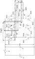
- FIG. 3 is a control example of the IGBT 3 in Phase 1 and an equivalent circuit diagram showing a current flow
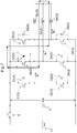
- FIG. It is the equivalent circuit diagram which similarly shows the example of control of IGBT3 in Phase2, and the flow of an electric current.
- the determination that the contactor is open may be performed based on, for example, communication from the vehicle ECU 90, or may be performed based on the detection result of the voltage sensor 14 that detects the DC link voltage Vdc.
- the determination that the contactor is open may be made based on a rapid change in the current (battery current) of the high-voltage battery 11 detected by the battery current sensor 15.
- the start of regenerative power suppression control is determined based on whether or not the DC link voltage Vdc detected by the voltage sensor 14 exceeds a determination threshold value for determining whether or not regenerative power suppression control is necessary. To do.
- ASC control is executed.
- FIG. 3 an example is shown in which lower-stage ASC control is executed.
- an IGBT 3 indicated by a broken line indicates that switching control is performed in an off state
- an IGBT 3 indicated by a solid line indicates that it is controlled in an on state.
- FWD5 indicated by a broken line indicates a non-conductive state
- FWD5 indicated by a solid line indicates a conductive state.
- the upper-stage IGBT (31, 33, 35) is controlled to be in an off state
- the lower-stage IGBT (32, 34, 36) is controlled to be in an on state.
- U-phase current Iu flows through U-phase lower stage IGBT 32.
- the V-phase current Iv flows through the V-phase lower stage IGBT 34 and also flows through the V-phase lower stage FWD 54 connected in reverse parallel to the V-phase lower stage IGBT 34.
- the W-phase current Iw flows through the W-phase lower-stage IGBT 36 and also flows through the W-phase lower-stage FWD 56 connected in reverse parallel to the W-phase lower-stage IGBT 36.
- PSD control is executed when the current (phase current) of any one phase arm (target arm) becomes zero during the Phase 1 period, that is, during execution of ASC control.
- the PSD control is preferably executed at time “t2” shown in FIG. 2, but is not strict and may be executed before and after time “t2”. Since the execution of the PSD control is delayed after detecting that the current has become zero, for example, the PSD control is preferably executed in anticipation of the phase current being zero.
- FIG. 2 illustrates an example in which PSD control is executed when the V-phase current Iv becomes zero in the Phase 1 period.
- the target arm is a V-phase arm, and the V-phase lower-stage IGBT 34 that is controlled to be in the ON state in the V-phase arm is controlled to be at least in the OFF state.
- the V phase is shut down and the inverter 10 is partially shut down (Phase 2).
- the electric power stored in the stator coil 8 charges the DC link capacitor 4 through the FWD 5, but the shutdown is performed with the phase current (Iv) being zero.
- the link voltage Vdc does not increase.
- the V-phase current Iv flows through the V-phase lower-stage IGBT 34 and also flows through the V-phase lower-stage FWD 54 connected in reverse parallel to the V-phase lower-stage IGBT 34. Therefore, when executing the PSD control, the inverter control device 20 is connected in parallel to the FWD 5 (54) when the current flowing through the forward conductive FWD 5 (here, the V-phase lower stage FWD 54) becomes zero. It can also be said that the IGBT 3 (here, the V-phase lower stage IGBT 34) is controlled to be in the OFF state.
- phase 2 since the V phase is shut down and the inverter 10 is partially shut down, the control performed from time “t2” is referred to as partial shutdown control (PSD control).
- PSD control partial shutdown control
- ASC control active short control
- PASC control partial active short control
- FIG. 4 shows a control example and current flow of the IGBT 3 in Phase 2.
- the U-phase current Iu flows through the U-phase lower-stage IGBT 32
- the W-phase current Iw flows through the W-phase lower-stage IGBT 36 and is connected to the W-phase lower-stage IGBT 36 in antiparallel.
- the lower stage FWD 56 also flows. Since the V-phase is shut down, the U-phase current Iu and the W-phase current Iw are balanced. Therefore, as shown in FIG. 2, the U-phase current Iu and the W-phase current Iw become zero at the same time (here, time “t3”).
- the inverter control device 20 controls all the remaining arms to the ON state when the currents of the two-phase arms (here, the U phase and the W phase) other than the target arm (here, the V phase) become zero.
- FSD control is performed to control the IGBT 3 (in this case, “32, 36”) to be turned off (FIG. 2: Phase 3).
- the shutdown is performed, the electric power stored in the stator coil 8 charges the DC link capacitor 4 via the FWD 5, but the shutdown is performed with the phase currents (Iu, Iw) being zero.
- the DC link voltage Vdc does not rise.
- the SD control As described above, by combining the SD control and the ASC control, it is possible to appropriately execute the control for making the current flowing through the rotating electrical machine 80 zero.
- the DC link voltage Vdc is reduced even if the capacitance of the DC link capacitor 4 is approximately 1 ⁇ 2. It has been confirmed that the rising voltage is about 1/5 to 1/4. In other words, the increase in the DC link voltage Vdc is suppressed by the regenerative power suppression control, and the DC link capacitor 4 can be downsized.
- the maximum value of the phase current is about 80% as compared with the case where the ASC control is simply executed in response to the contactor opening.
- phase current is also suppressed by the regenerative power suppression control. Therefore, it is possible to suppress a decrease in life due to the consumption of the stator coil 8 and the IGBT 3. That is, it has been confirmed by simulation that the rated current and the withstand voltage are satisfied under the conditions of the maximum regenerative power point and the maximum voltage of the inverter 10.
- the W-phase current Iw flows through the W-phase lower-stage IGBT 36 in both Phase 1 and Phase 2 and is connected to the W-phase lower-stage IGBT 36 in antiparallel with the W-phase lower-stage FWD 56. Also flows. That is, the W-phase current Iw circulates even when the W-phase lower stage IGBT 36 is in the OFF state in Phase2. Therefore, at the time of starting PSD control at time “t2”, the W-phase lower stage IGBT 36 may be controlled to be in the OFF state together with the V-phase lower stage IGBT 34. That is, the inverter control device 20 may execute PSD control as follows.
- the inverter control device 20 includes the IGBT 3 (here, “34”) that is controlled to be turned on in the target arm (here, V phase) and two phases (here, U phase, W phase) different from the target arm. ) Of the IGBTs 3 (32, 36) that are controlled to be in the ON state, and the IGBTs 3 (36) that are connected in parallel to the FWD 5 (here, “56”) that is conductive in the forward direction. PSD control may be executed by controlling to be in the off state. In other words, the inverter control device 20 is parallel to the forwardly conductive FWD 5 (here, “54, 56”) among the IGBTs 3 (here, “32, 34, 36”) controlled to be in the ON state. PSD control may be executed by controlling the two connected IGBTs 3 (here, “34, 36”) to be in an OFF state.
- the IGBT 3 that is in the on state in Phase 2 is only the U-phase lower stage IGBT 32. That is, when the FSD control is started at time “t3”, all of the remaining currents when the currents of the two-phase arms (here, the U-phase and the W-phase) other than the target arm (here, the V-phase) become zero are all.
- the only IGBT 3 that is controlled to be in the ON state is the U-phase lower stage IGBT 32.
- the inverter control device 20 makes all the remaining currents when the currents of the two-phase arms (here, the U phase and the W phase) different from the target arm (here, the V phase) become zero.
- the IGBT 3 that is controlled to be turned on in the arm the U-phase lower stage IGBT 32 is controlled to be turned off (FIG. 2: Phase 3).
- FIG. 5 is a waveform diagram schematically showing a control example when the contactor 9 is opened
- FIG. 6 is a control example of the IGBT 3 in Phase 1 and an equivalent circuit diagram showing a current flow
- FIG. It is the equivalent circuit diagram which similarly shows the example of control of IGBT3 in Phase2, and the flow of an electric current.
- ASC control is executed.
- the upper-stage ASC control is executed, the upper-stage IGBT (31, 33, 35) is controlled to be in the on state, and the lower-stage IGBT (32, 34, 36) is controlled to be in the off state. Is done.
- W-phase current Iw flows through W-phase upper stage IGBT 35.
- the U-phase current Iu flows through the U-phase upper stage IGBT 31 and also flows through the U-phase upper stage FWD 51 connected in reverse parallel to the U-phase upper stage IGBT 31.
- the V-phase current Iv flows through the V-phase upper stage IGBT 33 and also flows through the V-phase upper stage FWD 53 connected in reverse parallel to the V-phase upper stage IGBT 33.
- PSD control is executed when the current (phase current) of any one phase arm (target arm) becomes zero during the Phase 1 period, that is, during execution of ASC control.
- PSD control is executed when the U-phase current Iu becomes zero during the Phase 1 period.
- the target arm is a U-phase arm, and the U-phase upper stage IGBT 31 that is controlled to be in the ON state in the U-phase arm is controlled to be at least in the OFF state.
- the U phase is shut down, and the inverter 10 is partially shut down (Phase 2).
- the inverter 10 is partially shut down (Phase 2).
- the shutdown is performed, the electric power stored in the stator coil 8 charges the DC link capacitor 4 through the FWD 5, but the shutdown is performed with the phase current (Iu) being zero.
- the link voltage Vdc does not increase.
- the U-phase current Iu flows through the U-phase upper stage IGBT 31 and also flows through the U-phase upper stage FWD 51 connected in reverse parallel to the U-phase upper stage IGBT 31. Therefore, when the current flowing through the forward conductive FWD 5 (here, the U-phase upper stage FWD 51) becomes zero, the inverter control device 20 is connected to the FWD 5 (51) in parallel with the IGBT 3 (here U It can also be said that PSD control is executed by controlling the upper-phase IGBT 31) to be in the OFF state. Since this state is a state in which only two of the three phases are turned on, it can be referred to as two-phase switching control.
- FIG. 7 shows a control example of the IGBT 3 in Phase 2 and a current flow.
- the W-phase current Iw flows through the W-phase upper stage IGBT 35
- the V-phase current Iv flows through the V-phase upper stage IGBT 33 and is connected to the V-phase upper stage IGBT 33 in antiparallel.
- the upper FWD 53 also flows. Since the U phase is shut down, the V phase current Iv and the W phase current Iw are balanced. Therefore, the V-phase current Iv and the W-phase current Iw become zero at the same time (here, time “t3”).
- Inverter control device 20 controls all remaining arms to the ON state when the currents of two-phase arms (here, V-phase and W-phase) other than the target arm (here U-phase) become zero.
- FSD control is executed to control the IGBT 3 (in this case, “33, 35”) to be turned off (FIG. 5: Phase 3).
- the shutdown is performed, the electric power stored in the stator coil 8 charges the DC link capacitor 4 via the FWD 5, but the shutdown is performed with the phase currents (Iv, Iw) being zero.
- the DC link voltage Vdc does not rise.
- the V-phase current Iv flows through the V-phase upper stage IGBT 33 and is connected in reverse parallel to the V-phase upper stage IGBT 33. Also flows. That is, even in Phase 2, the V-phase current Iv circulates even when the V-phase upper stage IGBT 33 is in the OFF state. Therefore, when starting PSD control at time “t2”, the V-phase upper stage IGBT 33 may be controlled to be in the OFF state together with the U-phase upper stage IGBT 31.
- the inverter control device 20 includes the IGBT 3 (here, “31”) that is controlled to be turned on in the target arm (here, U phase) and two phases (here, V phase, W phase) different from the target arm. ) Of the IGBTs 3 (33, 35) controlled to be in the on state, the two IGBTs 3 including the IGBT 3 (33) connected in parallel to the forward FWD 5 (here, “53”) are connected. PSD control may be executed by controlling to be in the off state. In other words, the inverter control device 20 is parallel to the forwardly conductive FWD 5 (here, “51, 53”) among the IGBTs 3 (here, “31, 33, 35”) controlled to be in the on state. PSD control may be executed by controlling the two connected IGBTs 3 (here, “31, 33”) to be turned off.
- the IGBT 3 that is in the on state in Phase 2 is only the W-phase upper stage IGBT 35. Since this state is a state in which only one of the three phases is turned on, it can be referred to as single-phase switching control.
- the FSD control is started at time “t3”
- the currents of the two-phase arms here, the V phase and the W phase
- the target arm here, the U phase
- the inverter control device 20 makes all the remaining currents when the currents of the two-phase arms (here, the V phase and the W phase) different from the target arm (here, the U phase) become zero.
- the IGBT 3 that is controlled to be turned on in the arm the W-phase upper stage IGBT 35 is controlled to be turned off (FIG. 5: Phase 3).
- the ASC control executed in Phase 1 may be the upper-stage ASC control or the lower-stage ASC control.
- the inverter control device 20 preferably executes the ASC control by selecting either the upper-stage ASC control or the lower-stage ASC control according to the current phase of the three-phase arm. Specifically, as shown in FIG. 3, when the contactor is open (at time “t0”), when the three-phase current waveform has two phases on the positive side and one phase on the negative side, the lower-stage ASC control is performed. As shown in FIG. 6, when the contactor is open, if the three-phase current waveform is two-phase on the negative side and one-phase on the positive side, it is preferable that the upper-stage ASC control is selected. .
- Table 1 below shows the waveform of the three-phase current and the state of on / off control of each IGBT 3. As shown in Table 1, there are six states depending on the waveform of the three-phase current (Iu, Iv, Iw). This is indicated by Sector. “Su +, Sv +, Sw +, Su ⁇ , Sv ⁇ , Sw ⁇ ” in the table are U phase upper stage IGBT 31, V phase upper stage IGBT 33, W phase upper stage IGBT 35, U phase lower stage IGBT 32, V phase lower stage side, respectively. An IGBT 34 and a W-phase lower stage IGBT 36 are shown.
- Table 1 Three-phase current waveforms and switching element on / off control during ASC control
- the waveform of the three-phase current is two phases on the positive side and one phase on the negative side, there are two phases in which the lower-stage FWD 5 is conducting during the execution of the lower-stage ASC control.
- the three-phase current waveform is two phases on the negative side and one phase on the positive side, there are two phases in which the upper-stage FWD 5 is conducting during the execution of the upper-stage ASC control. Accordingly, when performing PSD control, the number of IGBTs 3 that can be controlled to be in the off state is one or two, so that control options increase.
- the two IGBTs 3 can be shifted from the on state to the off state at the time of the transition to the PSD control, the consumption of the IGBT 3 due to the large current flowing is suppressed, and the influence on the life is affected. It can also be reduced.
- the inverter control device 20 of the present embodiment executes regenerative power suppression control (SD-ASC mixed control) that appropriately sets the current flowing through the rotating electrical machine 80 to zero by combining SD control and ASC control.
- SD-ASC mixed control regenerative power suppression control
- FIG. 8 shows regions where the respective control methods are suitable on the operation map represented by the rotational speed and torque of the rotating electrical machine 80.
- EMF Electromotive Force
- a line “dg” represents a boundary where the back electromotive force (BEMF) is equal to or higher than the DC link voltage Vdc.
- SD control is suitable for the region where the rotation speed is low, that is, the region “0acdg” (region “R1 + R3”) in FIG. That is, the SD control is executed when the DC link voltage Vdc is larger than the electromotive force generated by the rotating electrical machine 80.
- the inverter control device 20 is constructed so that SD control is possible in all areas “0acdg” where this SD control is suitable, a design in consideration of the increase in the DC link voltage Vdc in that area is required.
- a switching element such as an IGBT 3 is required to have a high breakdown voltage
- the DC link capacitor 4 is also required to have a large capacity and a high breakdown voltage.
- the above-described regenerative power suppression control is preferably applied in the region “bcd” (region “R3”) in FIG.
- the active short control, the partial shutdown control, and the full shutdown control were illustrated in time series.
- the partial shutdown control and the full shutdown control may be executed in time series after the contactor 9 is opened without performing the active short control. That is, when the contactor 9 is opened, the partial shutdown control is started in the target arm, and then the full shutdown control is started when both currents of two-phase arms different from the target arm become zero. It only has to be done.
- the partial shutdown control is executed by selecting the target arm according to the current phase of the three-phase arm. For example, when the two-phase current waveform of the three phases is on the positive side of the amplitude center, the arm of the phase in which the current waveform is directed toward the amplitude center is selected as the target arm. Further, when the current waveform of two phases out of the three phases is on the negative side of the amplitude center, a phased arm whose current waveform is directed toward the amplitude center is selected as the target arm.
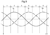
- FIG. 9 shows a current waveform when the rotating electrical machine 80 rotates forward.
- the numbers attached to the arrows in the figure represent the six states (Sector) corresponding to the waveforms of the three-phase currents (Iu, Iv, Iw), as in Table 1.
- the two-phase current waveform of the U-phase current Iu and the W-phase current Iw is on the positive side with respect to the amplitude center.
- the U-phase current Iu is directed to the peak of the current value
- the W-phase current Iw is directed to the amplitude center. Therefore, in Sector 1, the W-phase arm is the target arm.
- the IGBT 3 that is controlled to be on in the target arm is controlled to be off.
- all the IGBTs 3 (upper side IGBT and lower side IGBT) of the target arm are controlled to be in the off state.
- the W-phase upper stage IGBT 35 that is controlled to be in the on state is controlled to be in the off state. Since the W-phase lower stage IGBT 36 is in the OFF state in Sector 1, all the IGBTs 3 of the W-phase arm are turned off by controlling the W-phase upper stage IGBT 35 to the OFF state.
- the IGBT 3 of the U-phase arm different from the target arm among the two phases whose current waveform is on the positive side with respect to the amplitude center is switched.
- the U-phase upper-stage IGBT 31 is in an on state
- the U-phase lower-stage IGBT 32 is in an off state.
- the W-phase upper stage IGBT 35 as the target arm is controlled to be in the off state
- the U phase upper stage IGBT 31 is controlled to be in the off state
- the U phase lower stage IGBT 32 is controlled to be in the on state.
- this state is a state in which only two of the three phases are turned on, it is referred to as two-phase switching (Tow Phase Switching) control.
- two-phase switching Tow Phase Switching
- the two-phase current waveform of the U-phase current Iu and the V-phase current Iv is on the negative side of the amplitude center.
- the V-phase current Iv is directed to the negative peak of the current value
- the U-phase current Iu is directed to the amplitude center. Therefore, in Sector 6, the U-phase arm is the target arm.
- the U-phase lower-stage IGBT 32, the V-phase lower-stage IGBT 34, and the W-phase upper-stage IGBT 35 are on.
- the U-phase lower stage IGBT 32 is controlled to be in the off state, and the V-phase arm is controlled to be turned off by switching on / off of the upper-stage IGBT (33, 34).
- the IGBT 33 is controlled to be on.
- the ON / OFF state of the U-phase upper stage IGBT 31 and the W-phase upper and lower IGBTs (35, 36) is maintained.
- the partial shutdown control can be executed in the same state as when the active short control is performed.
- the inverter control device 20 targets the arm of the phase in which the current waveform is directed toward the amplitude center.
- the selected IGBT 3 is controlled to turn off the IGBT 3 that is turned on in the target arm, and further turns off the upper IGBT 3 in the phase different from the target arm in the two phases.
- the partial shutdown control is executed by controlling the lower IGBT 3 to be in the ON state.
- the inverter control device 20 uses the arm of the phase in which the current waveform is directed toward the amplitude center as the target arm.
- the IGBT 3 that is turned on in the target arm is controlled to be turned off, and further, the lower IGBT 3 of the arm different from the target arm in the two phases is turned off and the upper side
- the partial shutdown control is executed by controlling the IGBT 3 to be in the ON state. Table 2 below shows the waveforms of the three-phase current and the on / off control state of each switching element when the partial shutdown control is executed in the same state as when the active short control is performed.
- Table 2 Three-phase current waveforms and switching element ON / OFF control status during PSD control (when PSD control is executed simultaneously with ASC control)
- partial shutdown control is performed together with the partial active short control.
- the active short control and the partial active short control are performed after the contactor 9 is opened during the normal control.
- partial shutdown control and full shutdown control may be executed in time series.
- Table 3 shown below shows a waveform of a three-phase current and a state of on / off control of each switching element when executing partial shutdown control from normal control. A comparison between Table 2 and Table 3 shows that the partial shutdown control is executed without the partial active short control.
- Table 3 Three-phase current waveforms and switching element on / off control status during PSD control (when executing only PSD control from normal control)
- the target arm that is one of the phases of the target arm It is preferable that the partial shutdown control is started when the current becomes zero. As described above, when the current of the target arm is zero at the start of the partial shutdown control, the current flow is not hindered by the shutdown, and an increase in the DC link voltage Vdc is suppressed.
- the inverter control device 20 quickly determines that the contactor 9 is in the open state and starts the regenerative power suppression control. Therefore, in the above description, the state of the contactor 9 is not acquired via the vehicle ECU 90 by using CAN or the like that generally requires communication time, but based on the detection result of the DC link voltage Vdc, the contactor 9 can be quickly obtained. An example is shown in which it can be determined that is in an open state. As another aspect, the contactor is opened based on a sudden change in the current (battery current) of the high voltage battery 11 detected by the battery current sensor 15 provided between the high voltage battery 11 and the DC link capacitor 4.
- the inverter control device 20 determines that the contactor 9 is in the open state based on the detection result of the current of the high-voltage battery 11 rather than acquiring the state of the contactor 9 via the vehicle ECU 90 using CAN or the like. It is possible to quickly determine that it has become.
- DC link voltage Vdc DC link voltage
- DC link capacitor 4 smoothing capacitor
- the inverter control device (20) Connected to a DC power source via a contactor (9) and connected to an AC rotating electrical machine (80) to perform power conversion between DC and three-phase AC.
- An inverter (10) configured by a series circuit of a side switching element and a lower stage switching element, and a DC link capacitor for smoothing a DC link voltage (Vdc) which is a DC side voltage of the inverter (10) (4 ),
- An inverter control device (20) that controls the switching element (3) that constitutes the inverter (10) with a rotating electrical machine drive device (1) that includes the inverter (10) as a control target,
- the contactor (9) is in an open state during the rotation of the rotating electrical machine (80)
- the switching element (3) that is controlled to be on in any one of the target arms is turned off. Execute partial shutdown control to control Thereafter, when both of the currents of the two-phase arms different from the target arm become zero, the switching elements (3) that are controlled to be turned on in all the remaining arms are controlled to
- the target shutdown is selected according to the current phase of the three-phase arm, and the partial shutdown control is performed. Since the relative relationship of the current phases of the three-phase arms corresponds to the space vector (switching control state) of the inverter (10), an appropriate target arm can be selected according to the space vector (switching control state). it can.
- the inverter control device (20) has the arm of the phase in which the current waveform is directed toward the amplitude center. Is selected as the target arm, and when the current waveform of two phases out of the three phases is on the negative side of the amplitude center, the arm of the phase in which the current waveform is directed toward the amplitude center is selected as the target arm. It is preferable to select it as an arm. As the current of the arm to be shut down is closer to zero, the current flow is not hindered by the shutdown, and the increase of the DC link voltage (Vdc) is suppressed. Since the current at the amplitude center is zero, it is preferable to select the arm of the phase in which the current waveform goes to the amplitude center as the target arm.
- the inverter control device (20) is configured so that the arm of the phase different from the target arm is included in the two phases.
- the upper switching element (3) is turned off and the lower switching element (3) is controlled to be turned on, and two-phase current waveforms of the three phases are more negative than the amplitude center Is controlled so that the lower switching element (3) of the arm in a phase different from the target arm in the two phases is turned off and the upper switching element (3) is turned on. Then, it is preferable to execute the partial shutdown control.
- partial shutdown control is executed in the same state as when active short control is performed. can do. That is, by executing the active short control and the shutdown control at appropriate timing in time series, the current due to the active short control can be suppressed, and the voltage increase due to the shutdown control can be suppressed.
- the inverter control device (20) is configured such that when the contactor (9) is in an open state during the rotation of the rotating electrical machine (80), the upper-stage switching elements ( 3) Active short control of either the upper-stage active short-circuit control for turning on the lower-stage active short-circuit control for turning on the lower-stage switching elements (3) of the arms of all three phases is executed.
- the partial shutdown control may be executed after the active short control is started.
- the inverter control device (20) sets at least the switching element (3) controlled to be on in the target arm. It is preferable to execute the partial shutdown control by controlling. According to this aspect, since the current of the target arm is zero at the start of the partial shutdown control, the current flow is not hindered by the shutdown, and an increase in the DC link voltage (Vdc) is suppressed. Similarly, when the transition from the partial shutdown control to the full shutdown control is performed, since the current of the arm to be shut down is zero, the increase of the DC link voltage (Vdc) due to the shutdown is suppressed.
- the inverter (10) includes a free wheel diode (5) connected in parallel to each switching element (3) with the direction from the lower side to the upper side as a forward direction.
- the inverter control device (20) is configured so that the current flowing through the free wheel diode (5) in the forward conduction state becomes zero when the current flowing through the free wheel diode (5) becomes zero. It is preferable to execute the partial shutdown control by controlling the switching element (3) connected in parallel to the wheel diode (5) to be in an OFF state. Since the direction of the current is defined by the free wheel diode (5), the target arm can be easily identified. Further, in the target arm, when the current flowing through the free wheel diode (5) becomes zero, the current flowing through the switching element (3) also becomes zero. Therefore, the inverter control device (20) The switching element (3) can be controlled to be turned off.
- the inverter control device (20) selects any one of the upper-stage active short-circuit control and the lower-stage active short-circuit control according to the current phase of the three-phase arm, It is preferable to execute the active short control. Subsequent to the active short control, the partial shutdown control is executed. In the partial shutdown control, the current of the target arm needs to be zero. As the execution time of the active short control becomes longer, the large current flows back for a longer time. Therefore, it is preferable that the execution time of the active short control can be shortened. The time until the current of the target arm becomes zero after the start of the active short control depends on the three-phase current phase at the start of the active short control.
- the execution time of the active short control can be shortened by selecting either the upper-stage active short-circuit control or the lower-stage active short-circuit control according to the current phase of the three-phase arm. Can be shortened.
- the inverter control device (20) when two-phase current waveforms of the three phases are on the positive side with respect to the amplitude center, if the current waveform of two phases out of the three phases is more negative than the amplitude center, the upper-stage active short control Is preferably executed.
- the waveform of the three-phase current is two phases on the positive side and one phase on the negative side, there must be two phases in which the lower freewheel diode (5) is conducting during the execution of the lower active short-circuit control. become.
- the three-phase current waveform has two phases on the negative side and one phase on the positive side, there are two phases in which the upper freewheel diode is conducting during the execution of the upper active short-circuit control.
- the number of switching elements (3) that can be controlled to be in the off state is one or two, so that control options increase.
- the two switching elements (3) can be shifted from the on-state to the off-state, consumption of the switching elements (3) due to a large current flow is suppressed, and the lifetime is given. The influence can also be reduced.
- the inverter (10) includes a freewheel diode (5), and in a state where current flows through the freewheel diode (5) in a certain arm, the inverter (10) is connected in parallel to the freewheel diode (5). Even when the switching element (3) is in the OFF state, a current flows through the arm. Therefore, in the partial shutdown control, as long as current continues to flow through the free wheel diode (5), even if the arm is not the target arm, the switching element (3) is turned off together with the target arm. There is no.
- the inverter (10) includes a freewheel diode (5) connected in parallel to each switching element (3) with the direction from the lower side to the upper side as a forward direction
- the inverter control device ( 20) Among the switching element (3) controlled to be on in the target arm and the switching element (3) controlled to be on in the two-phase arm different from the target arm,
- the partial shutdown control is performed by controlling the switching element (3) connected in parallel with the free wheel diode (5) connected in parallel in the forward direction to turn off the two switching elements (3). It is preferable to execute.
- the present invention can be used for an inverter control device that drives and controls an AC rotating electric machine via an inverter.
Landscapes
- Engineering & Computer Science (AREA)
- Power Engineering (AREA)
- Life Sciences & Earth Sciences (AREA)
- Sustainable Development (AREA)
- Sustainable Energy (AREA)
- Transportation (AREA)
- Mechanical Engineering (AREA)
- Inverter Devices (AREA)
Abstract
Description
直流電源にコンタクタを介して接続されると共に交流の回転電機に接続されて直流と3相交流との間で電力変換を行うものであって交流1相分のアームが上段側スイッチング素子と下段側スイッチング素子との直列回路により構成されたインバータと、前記インバータの直流側の電圧である直流リンク電圧を平滑化する直流リンクコンデンサと、を備える回転電機駆動装置を制御対象として、前記インバータを構成するスイッチング素子をスイッチング制御するインバータ制御装置であって、
前記回転電機の回転中に前記コンタクタが開放状態となった場合に、何れか1相の前記アームである対象アームにおいてオン状態に制御されているスイッチング素子をオフ状態とするように制御するパーシャルシャットダウン制御を実行し、
その後、前記対象アームとは別の2相の前記アームの電流が共にゼロとなる際に残りの全ての前記アームにおいてオン状態に制御されているスイッチング素子をオフ状態とするように制御するフルシャットダウン制御を実行する点にある。
SD制御が実施された場合、ステータコイル8に蓄積された電力が、FWD5を介して直流リンクコンデンサ4を充電する。このため、直流リンクコンデンサ4の端子間電圧(直流リンク電圧Vdc)が短時間で上昇する可能性がある。直流リンク電圧Vdcの上昇に備えて直流リンクコンデンサ4を大容量化、高耐圧化すると、コンデンサの体格の増大につながる。また、インバータ10の高耐圧化も必要となる。その結果、回転電機駆動装置1の小型化の妨げとなり、部品コスト、製造コスト、製品コストにも影響する。

以下、その他の実施形態について説明する。尚、以下に説明する各実施形態の構成は、それぞれ単独で適用されるものに限られず、矛盾が生じない限り、他の実施形態の構成と組み合わせて適用することも可能である。
(ASC制御と同時にPSD制御を実行する場合)

(通常制御からPSD制御のみを実行する場合)

以下、上記において説明した実施形態に係るインバータ制御装置(20)の概要について簡単に説明する。
直流電源にコンタクタ(9)を介して接続されると共に交流の回転電機(80)に接続されて直流と3相交流との間で電力変換を行うものであって交流1相分のアームが上段側スイッチング素子と下段側スイッチング素子との直列回路により構成されたインバータ(10)と、前記インバータ(10)の直流側の電圧である直流リンク電圧(Vdc)を平滑化する直流リンクコンデンサと(4)、を備える回転電機駆動装置(1)を制御対象として、前記インバータ(10)を構成するスイッチング素子(3)をスイッチング制御するインバータ制御装置(20)であって、
前記回転電機(80)の回転中に前記コンタクタ(9)が開放状態となった場合に、何れか1相の前記アームである対象アームにおいてオン状態に制御されているスイッチング素子(3)をオフ状態とするように制御するパーシャルシャットダウン制御を実行し、
その後、前記対象アームとは別の2相の前記アームの電流が共にゼロとなる際に残りの全ての前記アームにおいてオン状態に制御されているスイッチング素子(3)をオフ状態とするように制御するフルシャットダウン制御を実行するように構成されている。
3 :IGBT(スイッチング素子)
4 :直流リンクコンデンサ
5 :フリーホイールダイオード
9 :コンタクタ
10 :インバータ
11 :高圧バッテリ(直流電源)
20 :インバータ制御装置
31~36:IGBT(スイッチング素子)
51~56:フリーホイールダイオード
80 :回転電機
Vdc :直流リンク電圧
Claims (10)
- 直流電源にコンタクタを介して接続されると共に交流の回転電機に接続されて直流と3相交流との間で電力変換を行うものであって交流1相分のアームが上段側スイッチング素子と下段側スイッチング素子との直列回路により構成されたインバータと、前記インバータの直流側の電圧である直流リンク電圧を平滑化する直流リンクコンデンサと、を備える回転電機駆動装置を制御対象として、前記インバータを構成するスイッチング素子をスイッチング制御するインバータ制御装置であって、
前記回転電機の回転中に前記コンタクタが開放状態となった場合に、何れか1相の前記アームである対象アームにおいてオン状態に制御されているスイッチング素子をオフ状態とするように制御するパーシャルシャットダウン制御を実行し、
その後、前記対象アームとは別の2相の前記アームの電流が共にゼロとなる際に残りの全ての前記アームにおいてオン状態に制御されているスイッチング素子をオフ状態とするように制御するフルシャットダウン制御を実行するインバータ制御装置。 - 3相の前記アームの電流位相に応じて、前記対象アームを選択して、前記パーシャルシャットダウン制御を実行する請求項1に記載のインバータ制御装置。
- 3相の内の2相の電流波形が振幅中心よりも正側の場合には、当該2相の内、電流波形が振幅中心に向かう相の前記アームを前記対象アームとして選択し、
3相の内の2相の電流波形が振幅中心よりも負側の場合には、当該2相の内、電流波形が振幅中心に向かう相の前記アームを前記対象アームとして選択する請求項2に記載のインバータ制御装置。 - 3相の内の2相の電流波形が振幅中心よりも正側の場合には、当該2相の内、前記対象アームとは異なる相の前記アームの前記上段側スイッチング素子をオフ状態とすると共に前記下段側スイッチング素子をオン状態とするように制御し、
3相の内の2相の電流波形が振幅中心よりも負側の場合には、当該2相の内、前記対象アームとは異なる相の前記アームの前記下段側スイッチング素子をオフ状態とすると共に前記上段側スイッチング素子をオン状態とするように制御して、前記パーシャルシャットダウン制御を実行する請求項3に記載のインバータ制御装置。 - 前記回転電機の回転中に前記コンタクタが開放状態となった場合に、3相全ての前記アームの前記上段側スイッチング素子をオン状態とする上段側アクティブショート制御、及び、3相全ての前記アームの前記下段側スイッチング素子をオン状態とする下段側アクティブショート制御の何れかのアクティブショート制御を実行し、
前記アクティブショート制御の開始後に、前記パーシャルシャットダウン制御を実行する請求項1から4の何れか一項に記載のインバータ制御装置。 - 前記対象アームの電流がゼロとなる際に、少なくとも前記対象アームにおいてオン状態に制御されている前記スイッチング素子をオフ状態とするように制御して、前記パーシャルシャットダウン制御を実行する請求項1から5の何れか一項に記載のインバータ制御装置。
- 前記インバータは、下段側から上段側へ向かう方向を順方向として各スイッチング素子に並列に接続されたフリーホイールダイオードを備えるものであり、
前記順方向に導通状態の前記フリーホイールダイオードに流れる電流がゼロとなる際に、当該フリーホイールダイオードに並列に接続された前記スイッチング素子をオフ状態となるように制御して、前記パーシャルシャットダウン制御を実行する請求項6に記載のインバータ制御装置。 - 3相の前記アームの電流位相に応じて、前記上段側アクティブショート制御、及び、前記下段側アクティブショート制御の何れかを選択して、前記アクティブショート制御を実行する請求項5から7の何れか一項に記載のインバータ制御装置。
- 前記アクティブショート制御の実行を開始する際に、3相の内の2相の電流波形が振幅中心よりも正側の場合には、前記下段側アクティブショート制御を実行し、
前記アクティブショート制御の実行を開始する際に、3相の内の2相の電流波形が振幅中心よりも負側の場合には、前記上段側アクティブショート制御を実行する、請求項8に記載のインバータ制御装置。 - 前記インバータは、下段側から上段側へ向かう方向を順方向として各スイッチング素子に並列に接続されたフリーホイールダイオードを備えるものであり、
前記対象アームにおいてオン状態に制御されているスイッチング素子と、前記対象アームとは別の2相の前記アームにおいてオン状態に制御されているスイッチング素子の内、前記順方向に導通状態の前記フリーホイールダイオードに並列接続されているスイッチング素子と、の2つのスイッチング素子をオフ状態とするように制御して、前記パーシャルシャットダウン制御を実行する請求項5から9の何れか一項に記載のインバータ制御装置。
Priority Applications (4)
| Application Number | Priority Date | Filing Date | Title |
|---|---|---|---|
| CN201580018171.XA CN106165277B (zh) | 2014-03-31 | 2015-03-26 | 逆变器控制装置 |
| JP2016511595A JP6256597B2 (ja) | 2014-03-31 | 2015-03-26 | インバータ制御装置 |
| US15/126,097 US9853591B2 (en) | 2014-03-31 | 2015-03-26 | Inverter control device |
| DE112015000834.9T DE112015000834T5 (de) | 2014-03-31 | 2015-03-26 | Wechselrichtersteuerungsvorrichtung |
Applications Claiming Priority (2)
| Application Number | Priority Date | Filing Date | Title |
|---|---|---|---|
| JP2014073588 | 2014-03-31 | ||
| JP2014-073588 | 2014-03-31 |
Publications (1)
| Publication Number | Publication Date |
|---|---|
| WO2015152002A1 true WO2015152002A1 (ja) | 2015-10-08 |
Family
ID=54240328
Family Applications (1)
| Application Number | Title | Priority Date | Filing Date |
|---|---|---|---|
| PCT/JP2015/059406 Ceased WO2015152002A1 (ja) | 2014-03-31 | 2015-03-26 | インバータ制御装置 |
Country Status (5)
| Country | Link |
|---|---|
| US (1) | US9853591B2 (ja) |
| JP (1) | JP6256597B2 (ja) |
| CN (1) | CN106165277B (ja) |
| DE (1) | DE112015000834T5 (ja) |
| WO (1) | WO2015152002A1 (ja) |
Cited By (4)
| Publication number | Priority date | Publication date | Assignee | Title |
|---|---|---|---|---|
| CN105514941A (zh) * | 2015-12-31 | 2016-04-20 | 联合汽车电子有限公司 | 电动汽车逆变器保护装置及其保护方法 |
| JP2017175772A (ja) * | 2016-03-23 | 2017-09-28 | アイシン・エィ・ダブリュ株式会社 | インバータ制御装置 |
| CN109874388A (zh) * | 2016-09-30 | 2019-06-11 | 弗罗纽斯国际有限公司 | 用于操作逆变器的方法及逆变器 |
| JP2022502989A (ja) * | 2018-09-20 | 2022-01-11 | ヴァレオ ジーメンス エーアオトモーティヴェ ゲルマニー ゲーエムベーハーValeo Siemens eAutomotive Germany GmbH | インバータの制御装置、非同期機用のインバータ、車両、及びインバータを動作させる方法 |
Families Citing this family (14)
| Publication number | Priority date | Publication date | Assignee | Title |
|---|---|---|---|---|
| US11296617B2 (en) * | 2017-09-28 | 2022-04-05 | Aisin Corporation | Inverter control device |
| EP3496250B1 (en) * | 2017-12-05 | 2022-05-11 | Valeo Siemens eAutomotive Germany GmbH | Inverter, assembly and vehicle comprising such inverter, and method for operating an inverter |
| EP3496249B1 (en) * | 2017-12-05 | 2023-01-04 | Valeo eAutomotive Germany GmbH | Inverter, assembly and vehicle comprising such inverter, and method for operating an inverter |
| GB201807771D0 (en) * | 2018-05-14 | 2018-06-27 | Rolls Royce Plc | Hybrid electric aircraft propulsion system |
| DE102018212192A1 (de) * | 2018-07-23 | 2020-01-23 | Audi Ag | Messvorrichtung zur Strommessung, Schaltungsanordnung, Filterelement und Kraftfahrzeug |
| DE102018123207A1 (de) * | 2018-09-20 | 2020-03-26 | Valeo Siemens Eautomotive Germany Gmbh | Steuerungseinrichtung für einen Wechselrichter, Wechselrichter für ein Fahrzeug, Fahrzeug und Verfahren zum Betreiben eines Wechselrichters |
| FR3097699B1 (fr) * | 2019-06-18 | 2021-07-16 | Alstom Transp Tech | Procédé d’inhibition d’un onduleur d’une chaîne d’alimentation en puissance électrique d’un moteur à aimants permanents |
| CN111092414B (zh) * | 2019-12-25 | 2022-03-29 | 深圳市英威腾电动汽车驱动技术有限公司 | 一种新能源汽车及其过压保护电路、过压保护方法 |
| JP2023052706A (ja) * | 2020-01-29 | 2023-04-12 | 日本電産エレシス株式会社 | モータ駆動回路 |
| CN111756279A (zh) * | 2020-06-12 | 2020-10-09 | 中车永济电机有限公司 | 电力机车永磁同步牵引电动机的反电势抑制方法及装置 |
| EP4075652B1 (en) * | 2021-04-14 | 2024-07-31 | Hitachi Energy Ltd | Inverter circuit for an electrical ac motor, electrical drive and method for controlling an electrical drive |
| DE102021214224A1 (de) * | 2021-12-13 | 2023-06-15 | Robert Bosch Gesellschaft mit beschränkter Haftung | Verfahren und Vorrichtung zum Betrieb eines Wechselrichters |
| DE102021214534A1 (de) | 2021-12-16 | 2023-06-22 | Brose Fahrzeugteile SE & Co. Kommanditgesellschaft, Würzburg | Verfahren zum Betrieb einer elektrischen Maschine |
| JP7679790B2 (ja) * | 2022-03-30 | 2025-05-20 | 株式会社豊田自動織機 | 電力変換システム |
Citations (3)
| Publication number | Priority date | Publication date | Assignee | Title |
|---|---|---|---|---|
| JP2008011670A (ja) * | 2006-06-30 | 2008-01-17 | Toyota Motor Corp | インバータ装置 |
| JP2010220287A (ja) * | 2009-03-13 | 2010-09-30 | Aisin Seiki Co Ltd | モータ制御装置および車両システム |
| JP2011055582A (ja) * | 2009-08-31 | 2011-03-17 | Denso Corp | 車載電動機の駆動装置 |
Family Cites Families (6)
| Publication number | Priority date | Publication date | Assignee | Title |
|---|---|---|---|---|
| DE2706395C3 (de) * | 1977-02-15 | 1979-09-27 | Siemens Ag, 1000 Berlin Und 8000 Muenchen | Unterbrechungsfreie Stromversorgungsanlage mit einem Wechselrichter |
| US4263535A (en) * | 1978-09-29 | 1981-04-21 | Bucyrus-Erie Company | Motor drive system for an electric mining shovel |
| US4654770A (en) * | 1983-12-22 | 1987-03-31 | General Electric Company | Current-limit circuit in X-ray generator |
| JP2004125209A (ja) * | 2002-09-30 | 2004-04-22 | Matsushita Electric Ind Co Ltd | 空気調和機 |
| DE102006003254A1 (de) * | 2006-01-24 | 2007-07-26 | Robert Bosch Gmbh | Verfahren zum Abschalten einer elektrischen Maschine im Falle einer Störung |
| JP2011109797A (ja) * | 2009-11-17 | 2011-06-02 | Hitachi Appliances Inc | 圧縮機用モータ駆動装置 |
-
2015
- 2015-03-26 US US15/126,097 patent/US9853591B2/en active Active
- 2015-03-26 WO PCT/JP2015/059406 patent/WO2015152002A1/ja not_active Ceased
- 2015-03-26 DE DE112015000834.9T patent/DE112015000834T5/de active Pending
- 2015-03-26 CN CN201580018171.XA patent/CN106165277B/zh active Active
- 2015-03-26 JP JP2016511595A patent/JP6256597B2/ja active Active
Patent Citations (3)
| Publication number | Priority date | Publication date | Assignee | Title |
|---|---|---|---|---|
| JP2008011670A (ja) * | 2006-06-30 | 2008-01-17 | Toyota Motor Corp | インバータ装置 |
| JP2010220287A (ja) * | 2009-03-13 | 2010-09-30 | Aisin Seiki Co Ltd | モータ制御装置および車両システム |
| JP2011055582A (ja) * | 2009-08-31 | 2011-03-17 | Denso Corp | 車載電動機の駆動装置 |
Cited By (7)
| Publication number | Priority date | Publication date | Assignee | Title |
|---|---|---|---|---|
| CN105514941A (zh) * | 2015-12-31 | 2016-04-20 | 联合汽车电子有限公司 | 电动汽车逆变器保护装置及其保护方法 |
| JP2017175772A (ja) * | 2016-03-23 | 2017-09-28 | アイシン・エィ・ダブリュ株式会社 | インバータ制御装置 |
| CN109874388A (zh) * | 2016-09-30 | 2019-06-11 | 弗罗纽斯国际有限公司 | 用于操作逆变器的方法及逆变器 |
| CN109874388B (zh) * | 2016-09-30 | 2020-01-14 | 弗罗纽斯国际有限公司 | 用于操作逆变器的方法及逆变器 |
| US10811996B2 (en) | 2016-09-30 | 2020-10-20 | Fronius Internationla GmbH | Method for operating an inverter, and inverter |
| JP2022502989A (ja) * | 2018-09-20 | 2022-01-11 | ヴァレオ ジーメンス エーアオトモーティヴェ ゲルマニー ゲーエムベーハーValeo Siemens eAutomotive Germany GmbH | インバータの制御装置、非同期機用のインバータ、車両、及びインバータを動作させる方法 |
| JP7530353B2 (ja) | 2018-09-20 | 2024-08-07 | ヴァレオ ジーメンス エーアオトモーティヴェ ゲルマニー ゲーエムベーハー | インバータの制御装置、非同期機用のインバータ、車両、及びインバータを動作させる方法 |
Also Published As
| Publication number | Publication date |
|---|---|
| JPWO2015152002A1 (ja) | 2017-04-13 |
| CN106165277B (zh) | 2018-10-23 |
| US9853591B2 (en) | 2017-12-26 |
| US20170093323A1 (en) | 2017-03-30 |
| CN106165277A (zh) | 2016-11-23 |
| JP6256597B2 (ja) | 2018-01-10 |
| DE112015000834T5 (de) | 2016-11-03 |
Similar Documents
| Publication | Publication Date | Title |
|---|---|---|
| JP6256597B2 (ja) | インバータ制御装置 | |
| CN106104998B (zh) | 逆变器控制装置 | |
| JP6307983B2 (ja) | インバータ制御装置 | |
| JP6169203B1 (ja) | 電動機制御装置および電動機制御方法 | |
| CN111095778B (zh) | 逆变器控制装置 | |
| JP6201867B2 (ja) | インバータ制御装置 | |
| JP6291899B2 (ja) | 回転電機制御装置 | |
| CN109104886B (zh) | 逆变器装置 | |
| CN110063012A (zh) | 逆变器控制装置 | |
| JP6253850B2 (ja) | 交流回転電機の制御装置 | |
| JP2016181949A (ja) | 電力変換装置 | |
| JP7244075B2 (ja) | 充電システム | |
| JP2017175747A (ja) | 電力変換装置 | |
| JP6305495B1 (ja) | インバータ制御装置及びインバータ制御方法 | |
| JP2017175772A (ja) | インバータ制御装置 | |
| JP2016181947A (ja) | 電力変換装置 | |
| CN111801887A (zh) | 旋转机驱动系统 | |
| JP6289597B1 (ja) | 車両用電源装置および車両用電源装置の制御方法 | |
| JP2020058177A (ja) | 充電制御方法および充電制御装置 | |
| JP2014165956A (ja) | 回転電機駆動装置 | |
| JP2021035090A (ja) | インバータ制御装置 | |
| JP5017529B2 (ja) | 磁石式同期モータ用電力変換装置 | |
| JP2025021579A (ja) | 車載充電装置 |
Legal Events
| Date | Code | Title | Description |
|---|---|---|---|
| 121 | Ep: the epo has been informed by wipo that ep was designated in this application |
Ref document number: 15774363 Country of ref document: EP Kind code of ref document: A1 |
|
| ENP | Entry into the national phase |
Ref document number: 2016511595 Country of ref document: JP Kind code of ref document: A |
|
| WWE | Wipo information: entry into national phase |
Ref document number: 15126097 Country of ref document: US Ref document number: 112015000834 Country of ref document: DE |
|
| 122 | Ep: pct application non-entry in european phase |
Ref document number: 15774363 Country of ref document: EP Kind code of ref document: A1 |