WO2015151273A1 - Semiconductor device - Google Patents
Semiconductor device Download PDFInfo
- Publication number
- WO2015151273A1 WO2015151273A1 PCT/JP2014/059974 JP2014059974W WO2015151273A1 WO 2015151273 A1 WO2015151273 A1 WO 2015151273A1 JP 2014059974 W JP2014059974 W JP 2014059974W WO 2015151273 A1 WO2015151273 A1 WO 2015151273A1
- Authority
- WO
- WIPO (PCT)
- Prior art keywords
- lead frame
- semiconductor device
- scale
- mold resin
- metal plating
- Prior art date
Links
Images


Classifications
-
- H—ELECTRICITY
- H01—ELECTRIC ELEMENTS
- H01L—SEMICONDUCTOR DEVICES NOT COVERED BY CLASS H10
- H01L23/00—Details of semiconductor or other solid state devices
- H01L23/562—Protection against mechanical damage
-
- H—ELECTRICITY
- H01—ELECTRIC ELEMENTS
- H01L—SEMICONDUCTOR DEVICES NOT COVERED BY CLASS H10
- H01L21/00—Processes or apparatus adapted for the manufacture or treatment of semiconductor or solid state devices or of parts thereof
- H01L21/02—Manufacture or treatment of semiconductor devices or of parts thereof
- H01L21/04—Manufacture or treatment of semiconductor devices or of parts thereof the devices having at least one potential-jump barrier or surface barrier, e.g. PN junction, depletion layer or carrier concentration layer
- H01L21/50—Assembly of semiconductor devices using processes or apparatus not provided for in a single one of the subgroups H01L21/06 - H01L21/326, e.g. sealing of a cap to a base of a container
- H01L21/56—Encapsulations, e.g. encapsulation layers, coatings
- H01L21/565—Moulds
-
- H—ELECTRICITY
- H01—ELECTRIC ELEMENTS
- H01L—SEMICONDUCTOR DEVICES NOT COVERED BY CLASS H10
- H01L23/00—Details of semiconductor or other solid state devices
- H01L23/28—Encapsulations, e.g. encapsulating layers, coatings, e.g. for protection
- H01L23/31—Encapsulations, e.g. encapsulating layers, coatings, e.g. for protection characterised by the arrangement or shape
- H01L23/3107—Encapsulations, e.g. encapsulating layers, coatings, e.g. for protection characterised by the arrangement or shape the device being completely enclosed
- H01L23/3114—Encapsulations, e.g. encapsulating layers, coatings, e.g. for protection characterised by the arrangement or shape the device being completely enclosed the device being a chip scale package, e.g. CSP
-
- H—ELECTRICITY
- H01—ELECTRIC ELEMENTS
- H01L—SEMICONDUCTOR DEVICES NOT COVERED BY CLASS H10
- H01L23/00—Details of semiconductor or other solid state devices
- H01L23/28—Encapsulations, e.g. encapsulating layers, coatings, e.g. for protection
- H01L23/31—Encapsulations, e.g. encapsulating layers, coatings, e.g. for protection characterised by the arrangement or shape
- H01L23/3107—Encapsulations, e.g. encapsulating layers, coatings, e.g. for protection characterised by the arrangement or shape the device being completely enclosed
- H01L23/3142—Sealing arrangements between parts, e.g. adhesion promotors
-
- H—ELECTRICITY
- H01—ELECTRIC ELEMENTS
- H01L—SEMICONDUCTOR DEVICES NOT COVERED BY CLASS H10
- H01L23/00—Details of semiconductor or other solid state devices
- H01L23/34—Arrangements for cooling, heating, ventilating or temperature compensation ; Temperature sensing arrangements
- H01L23/42—Fillings or auxiliary members in containers or encapsulations selected or arranged to facilitate heating or cooling
- H01L23/433—Auxiliary members in containers characterised by their shape, e.g. pistons
- H01L23/4334—Auxiliary members in encapsulations
-
- H—ELECTRICITY
- H01—ELECTRIC ELEMENTS
- H01L—SEMICONDUCTOR DEVICES NOT COVERED BY CLASS H10
- H01L23/00—Details of semiconductor or other solid state devices
- H01L23/48—Arrangements for conducting electric current to or from the solid state body in operation, e.g. leads, terminal arrangements ; Selection of materials therefor
- H01L23/488—Arrangements for conducting electric current to or from the solid state body in operation, e.g. leads, terminal arrangements ; Selection of materials therefor consisting of soldered or bonded constructions
- H01L23/495—Lead-frames or other flat leads
- H01L23/49503—Lead-frames or other flat leads characterised by the die pad
- H01L23/49513—Lead-frames or other flat leads characterised by the die pad having bonding material between chip and die pad
-
- H—ELECTRICITY
- H01—ELECTRIC ELEMENTS
- H01L—SEMICONDUCTOR DEVICES NOT COVERED BY CLASS H10
- H01L23/00—Details of semiconductor or other solid state devices
- H01L23/48—Arrangements for conducting electric current to or from the solid state body in operation, e.g. leads, terminal arrangements ; Selection of materials therefor
- H01L23/488—Arrangements for conducting electric current to or from the solid state body in operation, e.g. leads, terminal arrangements ; Selection of materials therefor consisting of soldered or bonded constructions
- H01L23/495—Lead-frames or other flat leads
- H01L23/49517—Additional leads
- H01L23/4952—Additional leads the additional leads being a bump or a wire
-
- H—ELECTRICITY
- H01—ELECTRIC ELEMENTS
- H01L—SEMICONDUCTOR DEVICES NOT COVERED BY CLASS H10
- H01L23/00—Details of semiconductor or other solid state devices
- H01L23/48—Arrangements for conducting electric current to or from the solid state body in operation, e.g. leads, terminal arrangements ; Selection of materials therefor
- H01L23/488—Arrangements for conducting electric current to or from the solid state body in operation, e.g. leads, terminal arrangements ; Selection of materials therefor consisting of soldered or bonded constructions
- H01L23/495—Lead-frames or other flat leads
- H01L23/49517—Additional leads
- H01L23/49524—Additional leads the additional leads being a tape carrier or flat leads
-
- H—ELECTRICITY
- H01—ELECTRIC ELEMENTS
- H01L—SEMICONDUCTOR DEVICES NOT COVERED BY CLASS H10
- H01L23/00—Details of semiconductor or other solid state devices
- H01L23/48—Arrangements for conducting electric current to or from the solid state body in operation, e.g. leads, terminal arrangements ; Selection of materials therefor
- H01L23/488—Arrangements for conducting electric current to or from the solid state body in operation, e.g. leads, terminal arrangements ; Selection of materials therefor consisting of soldered or bonded constructions
- H01L23/495—Lead-frames or other flat leads
- H01L23/49541—Geometry of the lead-frame
- H01L23/49548—Cross section geometry
-
- H—ELECTRICITY
- H01—ELECTRIC ELEMENTS
- H01L—SEMICONDUCTOR DEVICES NOT COVERED BY CLASS H10
- H01L23/00—Details of semiconductor or other solid state devices
- H01L23/48—Arrangements for conducting electric current to or from the solid state body in operation, e.g. leads, terminal arrangements ; Selection of materials therefor
- H01L23/488—Arrangements for conducting electric current to or from the solid state body in operation, e.g. leads, terminal arrangements ; Selection of materials therefor consisting of soldered or bonded constructions
- H01L23/495—Lead-frames or other flat leads
- H01L23/49579—Lead-frames or other flat leads characterised by the materials of the lead frames or layers thereon
- H01L23/49582—Metallic layers on lead frames
-
- H—ELECTRICITY
- H01—ELECTRIC ELEMENTS
- H01L—SEMICONDUCTOR DEVICES NOT COVERED BY CLASS H10
- H01L24/00—Arrangements for connecting or disconnecting semiconductor or solid-state bodies; Methods or apparatus related thereto
- H01L24/01—Means for bonding being attached to, or being formed on, the surface to be connected, e.g. chip-to-package, die-attach, "first-level" interconnects; Manufacturing methods related thereto
- H01L24/34—Strap connectors, e.g. copper straps for grounding power devices; Manufacturing methods related thereto
- H01L24/36—Structure, shape, material or disposition of the strap connectors prior to the connecting process
- H01L24/37—Structure, shape, material or disposition of the strap connectors prior to the connecting process of an individual strap connector
-
- H—ELECTRICITY
- H01—ELECTRIC ELEMENTS
- H01L—SEMICONDUCTOR DEVICES NOT COVERED BY CLASS H10
- H01L24/00—Arrangements for connecting or disconnecting semiconductor or solid-state bodies; Methods or apparatus related thereto
- H01L24/01—Means for bonding being attached to, or being formed on, the surface to be connected, e.g. chip-to-package, die-attach, "first-level" interconnects; Manufacturing methods related thereto
- H01L24/34—Strap connectors, e.g. copper straps for grounding power devices; Manufacturing methods related thereto
- H01L24/39—Structure, shape, material or disposition of the strap connectors after the connecting process
- H01L24/40—Structure, shape, material or disposition of the strap connectors after the connecting process of an individual strap connector
-
- H—ELECTRICITY
- H01—ELECTRIC ELEMENTS
- H01L—SEMICONDUCTOR DEVICES NOT COVERED BY CLASS H10
- H01L2224/00—Indexing scheme for arrangements for connecting or disconnecting semiconductor or solid-state bodies and methods related thereto as covered by H01L24/00
- H01L2224/01—Means for bonding being attached to, or being formed on, the surface to be connected, e.g. chip-to-package, die-attach, "first-level" interconnects; Manufacturing methods related thereto
- H01L2224/34—Strap connectors, e.g. copper straps for grounding power devices; Manufacturing methods related thereto
- H01L2224/36—Structure, shape, material or disposition of the strap connectors prior to the connecting process
- H01L2224/37—Structure, shape, material or disposition of the strap connectors prior to the connecting process of an individual strap connector
- H01L2224/37001—Core members of the connector
- H01L2224/37099—Material
- H01L2224/371—Material with a principal constituent of the material being a metal or a metalloid, e.g. boron [B], silicon [Si], germanium [Ge], arsenic [As], antimony [Sb], tellurium [Te] and polonium [Po], and alloys thereof
- H01L2224/37138—Material with a principal constituent of the material being a metal or a metalloid, e.g. boron [B], silicon [Si], germanium [Ge], arsenic [As], antimony [Sb], tellurium [Te] and polonium [Po], and alloys thereof the principal constituent melting at a temperature of greater than or equal to 950°C and less than 1550°C
- H01L2224/37147—Copper [Cu] as principal constituent
-
- H—ELECTRICITY
- H01—ELECTRIC ELEMENTS
- H01L—SEMICONDUCTOR DEVICES NOT COVERED BY CLASS H10
- H01L2224/00—Indexing scheme for arrangements for connecting or disconnecting semiconductor or solid-state bodies and methods related thereto as covered by H01L24/00
- H01L2224/01—Means for bonding being attached to, or being formed on, the surface to be connected, e.g. chip-to-package, die-attach, "first-level" interconnects; Manufacturing methods related thereto
- H01L2224/34—Strap connectors, e.g. copper straps for grounding power devices; Manufacturing methods related thereto
- H01L2224/39—Structure, shape, material or disposition of the strap connectors after the connecting process
- H01L2224/40—Structure, shape, material or disposition of the strap connectors after the connecting process of an individual strap connector
- H01L2224/4005—Shape
- H01L2224/4009—Loop shape
- H01L2224/40095—Kinked
-
- H—ELECTRICITY
- H01—ELECTRIC ELEMENTS
- H01L—SEMICONDUCTOR DEVICES NOT COVERED BY CLASS H10
- H01L2224/00—Indexing scheme for arrangements for connecting or disconnecting semiconductor or solid-state bodies and methods related thereto as covered by H01L24/00
- H01L2224/01—Means for bonding being attached to, or being formed on, the surface to be connected, e.g. chip-to-package, die-attach, "first-level" interconnects; Manufacturing methods related thereto
- H01L2224/34—Strap connectors, e.g. copper straps for grounding power devices; Manufacturing methods related thereto
- H01L2224/39—Structure, shape, material or disposition of the strap connectors after the connecting process
- H01L2224/40—Structure, shape, material or disposition of the strap connectors after the connecting process of an individual strap connector
- H01L2224/401—Disposition
- H01L2224/40151—Connecting between a semiconductor or solid-state body and an item not being a semiconductor or solid-state body, e.g. chip-to-substrate, chip-to-passive
- H01L2224/40221—Connecting between a semiconductor or solid-state body and an item not being a semiconductor or solid-state body, e.g. chip-to-substrate, chip-to-passive the body and the item being stacked
- H01L2224/40245—Connecting between a semiconductor or solid-state body and an item not being a semiconductor or solid-state body, e.g. chip-to-substrate, chip-to-passive the body and the item being stacked the item being metallic
-
- H—ELECTRICITY
- H01—ELECTRIC ELEMENTS
- H01L—SEMICONDUCTOR DEVICES NOT COVERED BY CLASS H10
- H01L2224/00—Indexing scheme for arrangements for connecting or disconnecting semiconductor or solid-state bodies and methods related thereto as covered by H01L24/00
- H01L2224/01—Means for bonding being attached to, or being formed on, the surface to be connected, e.g. chip-to-package, die-attach, "first-level" interconnects; Manufacturing methods related thereto
- H01L2224/42—Wire connectors; Manufacturing methods related thereto
- H01L2224/47—Structure, shape, material or disposition of the wire connectors after the connecting process
- H01L2224/48—Structure, shape, material or disposition of the wire connectors after the connecting process of an individual wire connector
- H01L2224/4805—Shape
- H01L2224/4809—Loop shape
- H01L2224/48091—Arched
-
- H—ELECTRICITY
- H01—ELECTRIC ELEMENTS
- H01L—SEMICONDUCTOR DEVICES NOT COVERED BY CLASS H10
- H01L2224/00—Indexing scheme for arrangements for connecting or disconnecting semiconductor or solid-state bodies and methods related thereto as covered by H01L24/00
- H01L2224/01—Means for bonding being attached to, or being formed on, the surface to be connected, e.g. chip-to-package, die-attach, "first-level" interconnects; Manufacturing methods related thereto
- H01L2224/42—Wire connectors; Manufacturing methods related thereto
- H01L2224/47—Structure, shape, material or disposition of the wire connectors after the connecting process
- H01L2224/48—Structure, shape, material or disposition of the wire connectors after the connecting process of an individual wire connector
- H01L2224/481—Disposition
- H01L2224/48151—Connecting between a semiconductor or solid-state body and an item not being a semiconductor or solid-state body, e.g. chip-to-substrate, chip-to-passive
- H01L2224/48221—Connecting between a semiconductor or solid-state body and an item not being a semiconductor or solid-state body, e.g. chip-to-substrate, chip-to-passive the body and the item being stacked
- H01L2224/48245—Connecting between a semiconductor or solid-state body and an item not being a semiconductor or solid-state body, e.g. chip-to-substrate, chip-to-passive the body and the item being stacked the item being metallic
- H01L2224/48247—Connecting between a semiconductor or solid-state body and an item not being a semiconductor or solid-state body, e.g. chip-to-substrate, chip-to-passive the body and the item being stacked the item being metallic connecting the wire to a bond pad of the item
-
- H—ELECTRICITY
- H01—ELECTRIC ELEMENTS
- H01L—SEMICONDUCTOR DEVICES NOT COVERED BY CLASS H10
- H01L2224/00—Indexing scheme for arrangements for connecting or disconnecting semiconductor or solid-state bodies and methods related thereto as covered by H01L24/00
- H01L2224/73—Means for bonding being of different types provided for in two or more of groups H01L2224/10, H01L2224/18, H01L2224/26, H01L2224/34, H01L2224/42, H01L2224/50, H01L2224/63, H01L2224/71
- H01L2224/732—Location after the connecting process
- H01L2224/73201—Location after the connecting process on the same surface
- H01L2224/73221—Strap and wire connectors
-
- H—ELECTRICITY
- H01—ELECTRIC ELEMENTS
- H01L—SEMICONDUCTOR DEVICES NOT COVERED BY CLASS H10
- H01L2224/00—Indexing scheme for arrangements for connecting or disconnecting semiconductor or solid-state bodies and methods related thereto as covered by H01L24/00
- H01L2224/73—Means for bonding being of different types provided for in two or more of groups H01L2224/10, H01L2224/18, H01L2224/26, H01L2224/34, H01L2224/42, H01L2224/50, H01L2224/63, H01L2224/71
- H01L2224/732—Location after the connecting process
- H01L2224/73251—Location after the connecting process on different surfaces
- H01L2224/73265—Layer and wire connectors
-
- H—ELECTRICITY
- H01—ELECTRIC ELEMENTS
- H01L—SEMICONDUCTOR DEVICES NOT COVERED BY CLASS H10
- H01L2224/00—Indexing scheme for arrangements for connecting or disconnecting semiconductor or solid-state bodies and methods related thereto as covered by H01L24/00
- H01L2224/80—Methods for connecting semiconductor or other solid state bodies using means for bonding being attached to, or being formed on, the surface to be connected
- H01L2224/84—Methods for connecting semiconductor or other solid state bodies using means for bonding being attached to, or being formed on, the surface to be connected using a strap connector
- H01L2224/848—Bonding techniques
- H01L2224/84801—Soldering or alloying
-
- H—ELECTRICITY
- H01—ELECTRIC ELEMENTS
- H01L—SEMICONDUCTOR DEVICES NOT COVERED BY CLASS H10
- H01L23/00—Details of semiconductor or other solid state devices
- H01L23/28—Encapsulations, e.g. encapsulating layers, coatings, e.g. for protection
- H01L23/31—Encapsulations, e.g. encapsulating layers, coatings, e.g. for protection characterised by the arrangement or shape
- H01L23/3107—Encapsulations, e.g. encapsulating layers, coatings, e.g. for protection characterised by the arrangement or shape the device being completely enclosed
-
- H—ELECTRICITY
- H01—ELECTRIC ELEMENTS
- H01L—SEMICONDUCTOR DEVICES NOT COVERED BY CLASS H10
- H01L24/00—Arrangements for connecting or disconnecting semiconductor or solid-state bodies; Methods or apparatus related thereto
- H01L24/80—Methods for connecting semiconductor or other solid state bodies using means for bonding being attached to, or being formed on, the surface to be connected
- H01L24/84—Methods for connecting semiconductor or other solid state bodies using means for bonding being attached to, or being formed on, the surface to be connected using a strap connector
-
- H—ELECTRICITY
- H01—ELECTRIC ELEMENTS
- H01L—SEMICONDUCTOR DEVICES NOT COVERED BY CLASS H10
- H01L2924/00—Indexing scheme for arrangements or methods for connecting or disconnecting semiconductor or solid-state bodies as covered by H01L24/00
- H01L2924/10—Details of semiconductor or other solid state devices to be connected
- H01L2924/11—Device type
- H01L2924/13—Discrete devices, e.g. 3 terminal devices
- H01L2924/1304—Transistor
- H01L2924/1305—Bipolar Junction Transistor [BJT]
- H01L2924/13055—Insulated gate bipolar transistor [IGBT]
-
- H—ELECTRICITY
- H01—ELECTRIC ELEMENTS
- H01L—SEMICONDUCTOR DEVICES NOT COVERED BY CLASS H10
- H01L2924/00—Indexing scheme for arrangements or methods for connecting or disconnecting semiconductor or solid-state bodies as covered by H01L24/00
- H01L2924/10—Details of semiconductor or other solid state devices to be connected
- H01L2924/11—Device type
- H01L2924/13—Discrete devices, e.g. 3 terminal devices
- H01L2924/1304—Transistor
- H01L2924/1306—Field-effect transistor [FET]
- H01L2924/13091—Metal-Oxide-Semiconductor Field-Effect Transistor [MOSFET]
-
- H—ELECTRICITY
- H01—ELECTRIC ELEMENTS
- H01L—SEMICONDUCTOR DEVICES NOT COVERED BY CLASS H10
- H01L2924/00—Indexing scheme for arrangements or methods for connecting or disconnecting semiconductor or solid-state bodies as covered by H01L24/00
- H01L2924/15—Details of package parts other than the semiconductor or other solid state devices to be connected
- H01L2924/181—Encapsulation
- H01L2924/183—Connection portion, e.g. seal
- H01L2924/18301—Connection portion, e.g. seal being an anchoring portion, i.e. mechanical interlocking between the encapsulation resin and another package part
Definitions
- the present invention relates to a resin mold type semiconductor device, and more particularly to improvement in adhesion between a lead frame and a mold resin.
- a copper plate or a copper alloy plate is used for a lead frame on which a semiconductor element is mounted, and the surface thereof is subjected to metal plating such as gold, silver, nickel, or tin for the purpose of improving corrosion resistance and heat resistance. Is done. Of these, nickel plating is often used.
- the adhesion with a mold resin such as an epoxy resin used for transfer molding may be lowered. For this reason, an initial peeling may occur between the lead frame and the mold resin immediately after transfer molding. Further, it is known that the mold resin is easily peeled from the lead frame due to repeated thermal stresses in the use environment.
- Patent Document 1 As a prior example having a configuration for improving the adhesion between the metal plating of the lead frame surface and the mold resin, in Patent Document 1, in a package component including at least a part of the surface covered with an insulating resin.
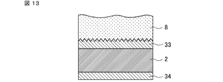
- the surface of the lead frame is covered with a conductive film, and the conductive film has a rough surface plating layer roughened on the coated surface (see FIG. 13).
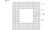
- Patent Document 2 a plurality of rectangular recesses are arranged vertically and horizontally at substantially equal intervals by so-called dimple processing in which a lead frame is pressed with a die, and the peeling of the mold resin is suppressed by an anchor effect (see FIG. 14).
- the rough plating layer of the package component disclosed in Patent Document 1 has a problem that the wire bonding property is inferior to that of the smooth plating layer. For this reason, the possibility that the bonding strength of the wire is reduced or unbonded increases.
- there is a method in which stripe plating or mask plating is partially applied to the connection portion with the wire but there is a problem that costs are increased as compared with full-surface plating.
- the rectangular recess of the semiconductor device disclosed in Patent Document 2 needs a width of about 200 ⁇ m in consideration of the dimple processing, and is difficult to process when a sufficient area cannot be secured in the lead frame.
- the vicinity of the connection portion of the lead frame with the wire is a region having a small area, and dimple processing cannot be performed.
- the semiconductor device is prevented from being downsized.
- the nickel plating has a higher hardness than copper, so the wear of the mold protrusions to form the square recesses is accelerated and the productivity decreases. There is a problem of doing.
- the lead frame is distorted by dimple processing, and the flatness of the lead frame cannot be secured.
- stress is generated due to distortion of the lead frame and damages to the solder and the electronic component. Therefore, it is essential to ensure the flatness of the lead frame.
- the present invention provides a semiconductor device that improves adhesion between a lead frame whose surface is metal-plated and a mold resin, can be downsized, and has high productivity and reliability. With the goal.
- a semiconductor device is a semiconductor device including a lead frame for mounting a semiconductor element and a mold resin for sealing at least a surface of the lead frame on which the semiconductor element is mounted.
- a region having a scale-like portion obtained by deforming the surface shape of the metal plating into a scale shape is provided in a region sealed with a mold resin.
- the adhesion effect between the lead frame and the mold resin can be improved by the anchor effect by the scale-like portion, and the mold resin can be prevented from peeling from the lead frame. Since the scale-like portion is a deformed surface of the metal plating, it can be easily placed at any location and does not impair the flatness of the lead frame during processing. A highly reliable semiconductor device can be obtained.
- FIG. 1 shows an example of the structure of a resin mold type semiconductor device according to the first embodiment.
- a semiconductor device 100 according to the first embodiment includes a semiconductor element 1, a lead frame 2, a wire 5, an inner lead 6, an external terminal 7, and the like.
- the same and corresponding parts are denoted by the same reference numerals in the drawings.
- the semiconductor element 1 is, for example, an IGBT, MOSFET, IC chip, LSI chip or the like, and is mounted on the upper surface of the lead frame 2 via a bonding member 4 such as solder or silver.
- the lead frame 2 on which the semiconductor element 1 or other electronic component is mounted is made of a copper plate or a copper alloy plate, and the surface thereof is coated with metal plating (not shown) such as gold, silver, nickel, tin or the like.
- the lead frame 2 has the scale-like part 3 which deform
- the scale portion 3 will be described in detail later.
- the electrode pad of the semiconductor element 1 is connected to the external terminal 7 via the wire 5 connected by wire bonding or the inner lead 6 made of a copper plate or copper alloy plate material.
- the wire 5 and the inner lead 6 can be replaced with each other.
- the wire 5 is made of gold, silver, aluminum, copper or the like and has a wire diameter of about 20 ⁇ m to 500 ⁇ m.
- At least the surface of the lead frame 2 on which the semiconductor element 1 is mounted is sealed with a molding resin 8 such as an epoxy resin by transfer molding.
- a molding resin 8 such as an epoxy resin by transfer molding.
- both surfaces of the lead frame 2 are sealed with a mold resin 8.
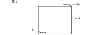
- a gate break mark 8 a is present at a predetermined location of the mold resin 8.
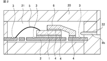
- FIG. 2 shows a transfer mold forming process in the manufacturing process of the semiconductor device 100.
- a lead frame 2 on which the semiconductor element 1 and other members are mounted is installed inside the molding die 20.
- the molten mold resin is injected into the cavity 21 of the molding die 20.
- the mold resin remaining in the gate 22 which is the path of the mold resin in the molding die 20 is called a runner 8b.
- a gate break for separating the runner 8b and the semiconductor device 100 is performed.
- a gate break mark 8a remains.
- initial peeling is likely to occur in a portion where the linear distance is the longest from the gate break mark 8a of the semiconductor device 100, that is, in the vicinity of the final filling portion of the mold resin. This is because the thermosetting mold resin 8 flows into the portion having the longest distance from the gate break mark 8a in the state where the viscosity is high and the wettability is poor, and therefore the adhesion to the lead frame 2 is poor. Is a factor.
- peeling may occur between the lead frame 2 and the mold resin 8 due to repeated thermal stress in the use environment.
- the bonding member 4 since the adhesion between the solder and the mold resin 8 is lower than that of other portions, the mold resin 8 is easily peeled off from the portion of the lead frame 2 where the solder adheres.
- the semiconductor device 100 has a scale-like portion 3 obtained by deforming the surface state of the metal plating covering the surface of the lead frame 2 into a scale shape. Yes. Due to the anchor effect of the scale-like portions 3, the adhesion between the metal plating and the mold resin 8 is enhanced, and the mold resin 8 is prevented from peeling off from the lead frame 2.
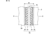
- FIG. 3 is a top view showing the scale portion 3 in the semiconductor device 100
- FIG. 4 is a cross-sectional view taken along the line AA shown in FIG. 3
- FIG. 5 is a portion taken along the line BB shown in FIG. It is sectional drawing cut
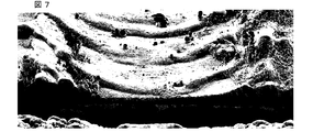
- disconnected by. 6 and 7 are diagrams obtained by scanning electron micrographs showing the form of the scaly portion 3.
- the scaly portion 3 is obtained by continuously irradiating the lead frame 2 with a spot by a laser so that the metal plating layer 30 is deformed into a scaly shape. As shown in FIG. They are arranged with a predetermined width W.
- the scaly portion 3 has a scaly portion 31 in which scaly projections are continuously arranged, and a raised portion 32 that rises higher than the scaly portion 31 on both sides of the scaly portion 31.
- the width W and height of the scaly portion 3 can be adjusted by laser output, scanning speed, and the like.
- the width W of the scale-like part 3 is, for example, about 60 ⁇ m, it may be increased according to the area of the place to be arranged. By increasing the width W of the scale portion 3, the adhesion with the mold resin 8 is further improved.
- the scaly portion 3 is disposed in the vicinity of the gate break mark 8 a of the lead frame 2, that is, in the vicinity of the gate 22 (see FIG. 2) of the molding die 20.
- the adhesive force between the metal plating layer 30 and the mold resin 8 in the vicinity of the gate break mark 8a where initial peeling is likely to occur can be improved.
- the scale portion 3 is disposed in the vicinity of a portion having the longest linear distance from the gate break mark 8 a of the lead frame 2.
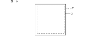
- the scale portion 3 is disposed on the outer peripheral portion in the region sealed with the mold resin 8 of the lead frame 2.
- the scale portion 3 is arranged around a portion of the lead frame 2 where the semiconductor element 1 is mounted.
- the joining member 4 is solder
- the scale portion 3 by arranging the scale portion 3 so as to surround the vicinity of the joining member 4, the solder wetting angle is increased, and the solder can be prevented from flowing out.
- the scale-like portion 3 is widely arranged in a region excluding the wire connecting portion 2 a of the lead frame 2.
- the wire bonding property is not deteriorated, and the wire 5 and the lead frame 2 can be favorably joined.
- the scaly portion 3 is formed by spot irradiation with a laser, it can be formed at any location on the lead frame 2. It is easy to selectively process only the place where the scale-like portion 3 is to be arranged and avoid the place where the scale-like portion 3 is not placed, for example, the wire connection portion 2a. In addition, when the processing pattern of the scale-like portion 3 is a single stroke as shown in FIGS. 8 to 12, the tact time can be shortened and the productivity is improved.
- FIGS As a comparative example of the semiconductor device 100 according to the first embodiment, a configuration for improving the adhesion between the lead frame and the mold resin in the conventional semiconductor device is shown in FIGS.
- a rough surface plating layer 33 having a surface profile roughened on the coating surface of the nickel plating layer is formed with a predetermined film thickness on the surface of the lead frame 2 on the mold resin 8 side. ing.
- the package component formed with such a rough plating layer 33 has improved adhesion between the lead frame 2 and the mold resin 8, and the adhesion does not deteriorate.
- the rough surface plating layer 33 is inferior in wire bonding compared to the smooth surface plating layer 34, there is a problem that the bonding strength of the wire is reduced and the possibility of unbonding is increased.
- the scale portion 3 in the semiconductor device 100 according to the first embodiment can be selectively formed at an arbitrary position on the lead frame 2, and avoids the wire connection portion 2 a of the lead frame 2. Therefore, it is advantageous in that the wire bonding property is not deteriorated.
- a plurality of rectangular recesses 9 are formed vertically and horizontally at substantially equal intervals in a region other than the die pad 2b of the lead frame 2 by dimple processing using a lead frame press die. . Also in the semiconductor device having such a configuration, the adhesion between the lead frame 2 and the mold resin is improved by the anchor effect by the rectangular recess 9.
- the square recess 9 needs to have a width of about 200 ⁇ m in consideration of the dimple processing, and depending on the design of the lead frame 2, a sufficient area cannot be secured and it is difficult to process.
- the scale portion 3 in the first embodiment can be formed in a narrow space of about 60 ⁇ m, and can contribute to the miniaturization of the semiconductor device. Further, since the scaly portion 3 is laser processed, a mold is not necessary, and it is not necessary to consider the wear of the protrusions of the mold, which is advantageous in terms of high productivity.
- the semiconductor device 100 when the semiconductor device 100 is inspected with an ultrasonic imaging apparatus or the like, it may be found that peeling is likely to occur at an unexpected location. In such a case, correcting the molding die 20 (refer to FIG. 2) or newly producing requires a great work period and cost.
- the scale portion 3 in the first embodiment is also effective against such a situation. That is, it can be selectively placed at a location where it has been found that peeling is likely to occur, and can be handled at low cost.
- the rectangular recess 9 has a gap between the adjacent rectangular recesses 9, there is a possibility that the solder for joining the semiconductor element flows out from the gap to the surroundings.
- the raised portion 32 of the scale portion 3 serves as a stopper and prevents the solder from flowing out. Great effect. Thereby, the position shift of the semiconductor element 1 can be suppressed.
- the method for manufacturing the semiconductor device 100 is not limited to this.
- an injection molding method may be used. In that case, since the cost of the resin is low, the cost can be reduced.
- the adhesion between the lead frame 2 and the mold resin 8 is improved by the anchor effect by the scale-like portion 3, and therefore the mold resin 8 is peeled from the lead frame 2. Can be suppressed.
- the scale-like portion 3 is formed by irradiating the lead frame 2 with a laser, it can be easily disposed at an arbitrary position, and the flatness of the lead frame 2 is not impaired during processing. For these reasons, according to the first embodiment, it is possible to obtain the semiconductor device 100 that can be miniaturized and has high productivity and reliability.
- FIG. 15 is a top view showing the scale portion 3a in the semiconductor device 100 according to the second embodiment
- FIG. 16 is a cross-sectional view taken along the line CC shown in FIG.
- the scale portion 3a in the second embodiment has a lead frame 2 under the metal plating layer 30, that is, an exposed portion 2c in which copper or a copper alloy is exposed, in the vicinity of the center portion of the predetermined width W.
- a lead frame 2 under the metal plating layer 30 that is, an exposed portion 2c in which copper or a copper alloy is exposed, in the vicinity of the center portion of the predetermined width W.
- the exposed copper or copper alloy has higher adhesion to the mold resin 8 than the metal plating layer 30, it is possible to further suppress the peeling of the mold resin as compared with the first embodiment.
- a method of raising the output of laser irradiation to completely melt the metal plating in the central portion as compared with the first embodiment, or shot blasting after laser treatment There is a method of scraping the metal plating by physical processing such as.
- the scale-like portion 3a is formed immediately before the transfer molding.
- the time for which copper is exposed is made as short as possible, it is easy to manage the degree of oxidation of copper, and it is possible to suppress an increase in cost.
- the exposed portion 2c in which copper or copper alloy having high adhesion to the mold resin 8 is exposed is provided at the central portion of the scale portion 3a.
- the effect of suppressing the peeling of the mold resin 8 from the lead frame 2 is higher than in the first embodiment.
- FIG. 17 shows the semiconductor device 101 according to the third embodiment.
- the semiconductor device 101 includes an electronic component 10 that is bridge-mounted so as to straddle between two spaced apart regions of the lead frame 2.
- the electronic component 10 is a capacitor, a thermistor, or the like.
- the two regions of the lead frame 2 on which the electronic component 10 is bridge-mounted are the region where the semiconductor element 1 is mounted and the region where the semiconductor element 1 is not mounted, and the two regions where the semiconductor element 1 is mounted. Either one region or two regions where the semiconductor element 1 is not mounted may be used.
- the scale portion 3 is provided by spot irradiation with a laser, and the flatness of the lead frame 2 is not impaired during processing.
- region of the lead frame 2 is about several tens of micrometers, and the flatness is ensured.
- the electronic component 10 is a capacitor serving as a noise filter
- the scale portion 3 on the lead frame 2 around the electronic component 10 it is possible to suppress peeling due to repeated thermal stress in a use environment that is likely to occur in the vicinity of the bonding member 4.
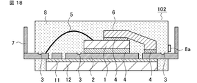
- FIG. 18 shows another semiconductor device 102 according to the third embodiment.
- a sheet 12 is attached to the lower part of the lead frame 2 via an adhesive member 11.
- the adhesive member 11 is grease, an adhesive, a resin adhesive, or the like.
- ceramic or silicone having electrical insulation and high thermal conductivity is used as the sheet 12.
- the adhesive member 11 has electrical insulation, copper having high thermal conductivity is used for the sheet 12. Furthermore, when attaching a heat sink, you may attach the sheet
- the scale portions 3 are provided in the semiconductor devices 101 and 102.
- the scale portions 3 a in which the lead frame 2 in the central portion is exposed may be provided.
- the scale-like parts 3 and 3a can be arranged at arbitrary positions as in the arrangement examples of FIGS. 8 to 12, for example.
- the same effect as in the first and second embodiments that is, the adhesion between the metal plating layer 30 and the mold resin 8 is enhanced, and the mold resin 8 peels from the lead frame 2.
- a semiconductor device that has high functionality and reliability, has a long lifetime, and can be reduced in size can be obtained.
- the configuration and manufacturing method of the semiconductor device to which the present invention is applied are not limited to the first to third embodiments.
- the present invention can be freely combined with each other within the scope of the invention, and each embodiment can be appropriately modified or omitted.
- the present invention can be used for a resin mold type semiconductor device.
Abstract
Description
この発明の上記以外の目的、特徴、観点及び効果は、図面を参照する以下のこの発明の詳細な説明から、さらに明らかになるであろう。 According to the semiconductor device of the present invention, the adhesion effect between the lead frame and the mold resin can be improved by the anchor effect by the scale-like portion, and the mold resin can be prevented from peeling from the lead frame. Since the scale-like portion is a deformed surface of the metal plating, it can be easily placed at any location and does not impair the flatness of the lead frame during processing. A highly reliable semiconductor device can be obtained.
Other objects, features, aspects and advantages of the present invention will become more apparent from the following detailed description of the present invention with reference to the drawings.
以下に、本発明の実施の形態1に係る半導体装置について、図面に基づいて説明する。図1に、本実施の形態1に係る樹脂モールド型の半導体装置の構造の一例を示す。本実施の形態1に係る半導体装置100は、半導体素子1、リードフレーム2、ワイヤ5、インナーリード6、および外部端子7等を含んで構成される。なお、以下の全ての図において、図中、同一、相当部分には同一符号を付している。
The semiconductor device according to the first embodiment of the present invention will be described below based on the drawings. FIG. 1 shows an example of the structure of a resin mold type semiconductor device according to the first embodiment. A
本発明の実施の形態2に係る半導体装置の全体構成は、上記実施の形態1と同様であるので図1を流用し、各部の説明を省略する。図15は、本実施の形態2に係る半導体装置100における鱗状部3aを示す上面図であり、図16は、図15に示すC-Cの部分で切断した断面図である。
Since the entire configuration of the semiconductor device according to the second embodiment of the present invention is the same as that of the first embodiment, FIG. 1 is used and the description of each part is omitted. FIG. 15 is a top view showing the
本発明の実施の形態3では、上記実施の形態1に係る半導体装置100とは構成の異なる半導体装置に鱗状部3を適用した例について説明する。図17は、本実施の形態3に係る半導体装置101を示している。半導体装置101は、リードフレーム2の離間された二つの領域の間を跨ぐようにブリッジ実装された電子部品10を備えている。電子部品10は、コンデンサやサーミスタ等である。
In the third embodiment of the present invention, an example in which the
Claims (10)
- 半導体素子を搭載するリードフレームと、前記リードフレームの少なくとも前記半導体素子を搭載した面を封止するモールド樹脂を備えた半導体装置であって、
前記リードフレームは、その表面を部分的または全体的に金属めっきで被覆されると共に、前記モールド樹脂により封止される領域内に、前記金属めっきの表面形状を鱗状に変形させた鱗状部を有することを特徴とする半導体装置。 A semiconductor device comprising: a lead frame for mounting a semiconductor element; and a mold resin for sealing at least a surface of the lead frame on which the semiconductor element is mounted;
The lead frame has a scale-like portion in which the surface of the metal plating is deformed into a scale shape in a region where the surface is partially or entirely covered with metal plating and sealed with the mold resin. A semiconductor device. - 前記鱗状部は、任意の直線上または曲線上に所定幅で配置されることを特徴とする請求項1記載の半導体装置。 2. The semiconductor device according to claim 1, wherein the scale portions are arranged with a predetermined width on an arbitrary straight line or curve.
- 前記鱗状部は、前記所定幅の中央部付近において、前記金属めっきの下の前記リードフレームが露出していることを特徴とする請求項2記載の半導体装置。 3. The semiconductor device according to claim 2, wherein the scale-like portion exposes the lead frame under the metal plating in the vicinity of the central portion of the predetermined width.
- 前記モールド樹脂による封止の際に用いられる成形金型は、溶融された前記モールド樹脂の通り道であるゲートを有し、前記鱗状部は、前記リードフレームの前記ゲートに近接する箇所に配置されることを特徴とする請求項1から請求項3のいずれか一項に記載の半導体装置。 A molding die used for sealing with the mold resin has a gate that is a passage for the melted mold resin, and the scale portion is disposed at a location near the gate of the lead frame. The semiconductor device according to claim 1, wherein the semiconductor device is a semiconductor device.
- 前記モールド樹脂による封止の際に用いられる成形金型は、溶融された前記モールド樹脂の通り道であるゲートを有し、前記鱗状部は、前記リードフレームの前記ゲートから最も直線距離が長い箇所の付近に配置されることを特徴とする請求項1から請求項4のいずれか一項に記載の半導体装置。 A molding die used for sealing with the mold resin has a gate that is a passage for the molten mold resin, and the scale portion has a longest linear distance from the gate of the lead frame. The semiconductor device according to claim 1, wherein the semiconductor device is disposed in the vicinity.
- 前記鱗状部は、前記リードフレームの前記モールド樹脂により封止される領域内の外周部に配置されることを特徴とする請求項1から請求項5のいずれか一項に記載の半導体装置。 The semiconductor device according to any one of claims 1 to 5, wherein the scale portion is disposed on an outer peripheral portion in a region sealed with the mold resin of the lead frame.
- 前記鱗状部は、前記リードフレームの前記半導体素子を搭載した箇所の周囲に配置されることを特徴とする請求項1から請求項6のいずれか一項に記載の半導体装置。 The semiconductor device according to any one of claims 1 to 6, wherein the scale portion is arranged around a portion of the lead frame where the semiconductor element is mounted.
- 前記半導体素子と前記リードフレームの所定の箇所とを電気的に接続するワイヤを有し、前記鱗状部は、前記リードフレームの前記ワイヤとの接続部を除く領域に配置されることを特徴とする請求項1から請求項7のいずれか一項に記載の半導体装置。 It has a wire for electrically connecting the semiconductor element and a predetermined portion of the lead frame, and the scale portion is arranged in a region excluding the connection portion with the wire of the lead frame. The semiconductor device according to claim 1.
- 前記リードフレームの離間された二つの領域を跨ぐようにブリッジ実装された電子部品を有し、前記鱗状部は、前記リードフレームの前記電子部品を搭載した箇所の周囲に配置されることを特徴とする請求項1から請求項8のいずれか一項に記載の半導体装置。 It has an electronic component that is bridge-mounted so as to straddle two spaced apart regions of the lead frame, and the scale portion is arranged around a portion of the lead frame where the electronic component is mounted. The semiconductor device according to any one of claims 1 to 8.
- 前記鱗状部は、前記リードフレームにレーザーを照射することにより前記金属めっきを変形させたものであることを特徴とする請求項1から請求項9のいずれか一項に記載の半導体装置。 The semiconductor device according to any one of claims 1 to 9, wherein the scale portion is formed by deforming the metal plating by irradiating the lead frame with a laser.
Priority Applications (5)
| Application Number | Priority Date | Filing Date | Title |
|---|---|---|---|
| JP2016511284A JP6150938B2 (en) | 2014-04-04 | 2014-04-04 | Semiconductor device |
| PCT/JP2014/059974 WO2015151273A1 (en) | 2014-04-04 | 2014-04-04 | Semiconductor device |
| CN201480077767.2A CN106471617B (en) | 2014-04-04 | 2014-04-04 | Semiconductor device |
| EP14887816.8A EP3128550B1 (en) | 2014-04-04 | 2014-04-04 | Semiconductor device |
| US15/104,750 US9899336B2 (en) | 2014-04-04 | 2014-04-04 | Semiconductor device |
Applications Claiming Priority (1)
| Application Number | Priority Date | Filing Date | Title |
|---|---|---|---|
| PCT/JP2014/059974 WO2015151273A1 (en) | 2014-04-04 | 2014-04-04 | Semiconductor device |
Publications (1)
| Publication Number | Publication Date |
|---|---|
| WO2015151273A1 true WO2015151273A1 (en) | 2015-10-08 |
Family
ID=54239633
Family Applications (1)
| Application Number | Title | Priority Date | Filing Date |
|---|---|---|---|
| PCT/JP2014/059974 WO2015151273A1 (en) | 2014-04-04 | 2014-04-04 | Semiconductor device |
Country Status (5)
| Country | Link |
|---|---|
| US (1) | US9899336B2 (en) |
| EP (1) | EP3128550B1 (en) |
| JP (1) | JP6150938B2 (en) |
| CN (1) | CN106471617B (en) |
| WO (1) | WO2015151273A1 (en) |
Cited By (8)
| Publication number | Priority date | Publication date | Assignee | Title |
|---|---|---|---|---|
| WO2017154072A1 (en) * | 2016-03-07 | 2017-09-14 | 三菱電機株式会社 | Semiconductor device and method for manufacturing semiconductor device |
| WO2017169485A1 (en) * | 2016-03-30 | 2017-10-05 | パナソニックIpマネジメント株式会社 | Semiconductor device |
| WO2017175542A1 (en) * | 2016-04-04 | 2017-10-12 | 株式会社デンソー | Electronic device and method for manufacturing same |
| JP2017191857A (en) * | 2016-04-13 | 2017-10-19 | 株式会社デンソー | Electronic device and manufacturing method of the same |
| JP2018157023A (en) * | 2017-03-16 | 2018-10-04 | 株式会社デンソー | Semiconductor device and method of manufacturing the same |
| WO2020049672A1 (en) * | 2018-09-06 | 2020-03-12 | 三菱電機株式会社 | Semiconductor device |
| DE112015001933B4 (en) | 2014-04-23 | 2023-06-07 | Denso Corporation | semiconductor device |
| WO2023243256A1 (en) * | 2022-06-13 | 2023-12-21 | 富士電機株式会社 | Semiconductor device |
Families Citing this family (12)
| Publication number | Priority date | Publication date | Assignee | Title |
|---|---|---|---|---|
| KR101862705B1 (en) * | 2017-09-29 | 2018-05-30 | 제엠제코(주) | Clip and leadframe for semiconductor package with finely engraved patterns and the semiconductor package having the same |
| TWI746883B (en) | 2017-09-29 | 2021-11-21 | 韓商Jmj韓國有限公司 | Clip, leadframe and substrate for semiconductor package with finely engraved patterns and the semiconductor package having the same |
| DE112017008277T5 (en) * | 2017-12-13 | 2020-08-20 | Mitsubishi Electric Corporation | SEMICONDUCTOR DEVICE AND POWER CONVERSION DEVICE |
| JP6777063B2 (en) * | 2017-12-20 | 2020-10-28 | 株式会社デンソー | Electronic devices and their manufacturing methods |
| US10777489B2 (en) | 2018-05-29 | 2020-09-15 | Katoh Electric Co., Ltd. | Semiconductor module |
| JP6437700B1 (en) | 2018-05-29 | 2018-12-12 | 新電元工業株式会社 | Semiconductor module |
| CN110914981B (en) * | 2018-05-29 | 2023-06-16 | 新电元工业株式会社 | Semiconductor module |
| CN112805814A (en) * | 2018-10-16 | 2021-05-14 | 三菱电机株式会社 | Power semiconductor device and method for manufacturing the same |
| KR102125148B1 (en) * | 2018-12-05 | 2020-06-19 | 한양대학교 에리카산학협력단 | Manufacturing method of engraved pattern and nano metal coated layer produced by the method |
| US10937744B2 (en) | 2019-02-22 | 2021-03-02 | Infineon Technologies Ag | Semiconductor packages including roughening features |
| JP2021174883A (en) * | 2020-04-24 | 2021-11-01 | Jx金属株式会社 | Metal plate, metal resin composite body and semiconductor device |
| JP7097933B2 (en) * | 2020-10-08 | 2022-07-08 | 三菱電機株式会社 | Manufacturing method of semiconductor device |
Citations (3)
| Publication number | Priority date | Publication date | Assignee | Title |
|---|---|---|---|---|
| JP2006032775A (en) * | 2004-07-20 | 2006-02-02 | Denso Corp | Electronic device |
| JP2010161098A (en) * | 2009-01-06 | 2010-07-22 | Nichiden Seimitsu Kogyo Kk | Method of manufacturing lead frame, lead frame, method of manufacturing heat sink, and heat sink |
| JP2013153032A (en) * | 2012-01-25 | 2013-08-08 | Panasonic Corp | Manufacturing method of led package |
Family Cites Families (8)
| Publication number | Priority date | Publication date | Assignee | Title |
|---|---|---|---|---|
| JP3748849B2 (en) | 2002-12-06 | 2006-02-22 | 三菱電機株式会社 | Resin-sealed semiconductor device |
| EP1905077B1 (en) * | 2005-07-08 | 2012-05-23 | Nxp B.V. | Semiconductor device |
| US8012886B2 (en) * | 2007-03-07 | 2011-09-06 | Asm Assembly Materials Ltd | Leadframe treatment for enhancing adhesion of encapsulant thereto |
| US8044495B2 (en) * | 2009-06-22 | 2011-10-25 | Texas Instruments Incorporated | Metallic leadframes having laser-treated surfaces for improved adhesion to polymeric compounds |
| WO2012049742A1 (en) * | 2010-10-13 | 2012-04-19 | 日立オートモティブシステムズ株式会社 | Flow sensor and production method therefor, and flow sensor module and production method therefor |
| JP5264939B2 (en) | 2011-01-14 | 2013-08-14 | 新光電気工業株式会社 | Package parts and semiconductor packages |
| JP5863174B2 (en) * | 2012-03-01 | 2016-02-16 | ルネサスエレクトロニクス株式会社 | Manufacturing method of semiconductor device |
| JP6102187B2 (en) * | 2012-10-31 | 2017-03-29 | 日亜化学工業株式会社 | Light emitting device package and light emitting device using the same |
-
2014
- 2014-04-04 CN CN201480077767.2A patent/CN106471617B/en active Active
- 2014-04-04 EP EP14887816.8A patent/EP3128550B1/en active Active
- 2014-04-04 WO PCT/JP2014/059974 patent/WO2015151273A1/en active Application Filing
- 2014-04-04 US US15/104,750 patent/US9899336B2/en active Active
- 2014-04-04 JP JP2016511284A patent/JP6150938B2/en active Active
Patent Citations (3)
| Publication number | Priority date | Publication date | Assignee | Title |
|---|---|---|---|---|
| JP2006032775A (en) * | 2004-07-20 | 2006-02-02 | Denso Corp | Electronic device |
| JP2010161098A (en) * | 2009-01-06 | 2010-07-22 | Nichiden Seimitsu Kogyo Kk | Method of manufacturing lead frame, lead frame, method of manufacturing heat sink, and heat sink |
| JP2013153032A (en) * | 2012-01-25 | 2013-08-08 | Panasonic Corp | Manufacturing method of led package |
Non-Patent Citations (1)
| Title |
|---|
| See also references of EP3128550A4 * |
Cited By (20)
| Publication number | Priority date | Publication date | Assignee | Title |
|---|---|---|---|---|
| DE112015001933B4 (en) | 2014-04-23 | 2023-06-07 | Denso Corporation | semiconductor device |
| JPWO2017154072A1 (en) * | 2016-03-07 | 2018-05-10 | 三菱電機株式会社 | Semiconductor device and manufacturing method of semiconductor device |
| US11152275B2 (en) | 2016-03-07 | 2021-10-19 | Mitsubishi Electric Corporation | Semiconductor device and method for manufacturing semiconductor device |
| EP3428962A4 (en) * | 2016-03-07 | 2019-07-10 | Mitsubishi Electric Corporation | Semiconductor device and method for manufacturing semiconductor device |
| WO2017154072A1 (en) * | 2016-03-07 | 2017-09-14 | 三菱電機株式会社 | Semiconductor device and method for manufacturing semiconductor device |
| CN108701661A (en) * | 2016-03-07 | 2018-10-23 | 三菱电机株式会社 | The manufacturing method of semiconductor device and semiconductor device |
| US10297516B2 (en) | 2016-03-30 | 2019-05-21 | Panasonic Intellectual Property Management Co., Ltd. | Semiconductor device |
| CN107924884B (en) * | 2016-03-30 | 2022-02-18 | 松下知识产权经营株式会社 | Semiconductor device with a plurality of semiconductor chips |
| CN107924884A (en) * | 2016-03-30 | 2018-04-17 | 松下知识产权经营株式会社 | Semiconductor device |
| WO2017169485A1 (en) * | 2016-03-30 | 2017-10-05 | パナソニックIpマネジメント株式会社 | Semiconductor device |
| JPWO2017169485A1 (en) * | 2016-03-30 | 2018-07-12 | パナソニックIpマネジメント株式会社 | Semiconductor device |
| JP2017188534A (en) * | 2016-04-04 | 2017-10-12 | 株式会社デンソー | Electronic device and method of manufacturing the same |
| WO2017175542A1 (en) * | 2016-04-04 | 2017-10-12 | 株式会社デンソー | Electronic device and method for manufacturing same |
| JP2017191857A (en) * | 2016-04-13 | 2017-10-19 | 株式会社デンソー | Electronic device and manufacturing method of the same |
| JP2018157023A (en) * | 2017-03-16 | 2018-10-04 | 株式会社デンソー | Semiconductor device and method of manufacturing the same |
| JPWO2020049672A1 (en) * | 2018-09-06 | 2021-08-12 | 三菱電機株式会社 | Semiconductor device |
| JP7090716B2 (en) | 2018-09-06 | 2022-06-24 | 三菱電機株式会社 | Semiconductor equipment |
| WO2020049672A1 (en) * | 2018-09-06 | 2020-03-12 | 三菱電機株式会社 | Semiconductor device |
| US11837516B2 (en) | 2018-09-06 | 2023-12-05 | Mitsubishi Electric Corporation | Semiconductor device |
| WO2023243256A1 (en) * | 2022-06-13 | 2023-12-21 | 富士電機株式会社 | Semiconductor device |
Also Published As
| Publication number | Publication date |
|---|---|
| EP3128550A4 (en) | 2018-01-10 |
| EP3128550B1 (en) | 2020-11-04 |
| JPWO2015151273A1 (en) | 2017-04-13 |
| JP6150938B2 (en) | 2017-06-21 |
| CN106471617A (en) | 2017-03-01 |
| CN106471617B (en) | 2019-05-10 |
| EP3128550A1 (en) | 2017-02-08 |
| US9899336B2 (en) | 2018-02-20 |
| US20160315054A1 (en) | 2016-10-27 |
Similar Documents
| Publication | Publication Date | Title |
|---|---|---|
| JP6150938B2 (en) | Semiconductor device | |
| JP6193510B2 (en) | Lead frame, semiconductor device, lead frame manufacturing method, and semiconductor device manufacturing method | |
| JP6309112B2 (en) | Power module | |
| JP6345342B2 (en) | Semiconductor device | |
| US20150228563A1 (en) | Lead frame with abutment surface | |
| JP6266168B2 (en) | Semiconductor device | |
| JP2006222406A (en) | Semiconductor device | |
| JP5854011B2 (en) | Semiconductor device and manufacturing method of semiconductor device | |
| JP2009277949A (en) | Semiconductor device and method of manufacturing the same | |
| US8581378B2 (en) | Semiconductor device and method of manufacturing the same | |
| JP2014090103A (en) | Molded package and method for manufacturing the same | |
| JP6702800B2 (en) | Circuit board assembly, electronic device assembly, circuit board assembly manufacturing method, and electronic device manufacturing method | |
| JP2003133329A (en) | Semiconductor device | |
| JP7090716B2 (en) | Semiconductor equipment | |
| JP2006191143A (en) | Semiconductor device | |
| JP6869602B2 (en) | Semiconductor device | |
| JP6064845B2 (en) | Semiconductor device | |
| US9147646B2 (en) | Lead frame, method for manufacturing lead frame and semiconductor device using same | |
| JP2016219707A (en) | Semiconductor device and manufacturing method of the same | |
| JP2017050441A (en) | Semiconductor device | |
| JP6407042B2 (en) | Semiconductor device and manufacturing method thereof | |
| WO2015129185A1 (en) | Resin-sealed semiconductor device, production method therefor, and mounting body therefor | |
| JP4653608B2 (en) | Manufacturing method of surface mount type resin hollow package | |
| JP4695672B2 (en) | Semiconductor device | |
| KR20070103591A (en) | Semiconductor package having insulator interposed between leads and method of fabricating semiconductor device having the same |
Legal Events
| Date | Code | Title | Description |
|---|---|---|---|
| 121 | Ep: the epo has been informed by wipo that ep was designated in this application |
Ref document number: 14887816 Country of ref document: EP Kind code of ref document: A1 |
|
| ENP | Entry into the national phase |
Ref document number: 2016511284 Country of ref document: JP Kind code of ref document: A |
|
| REEP | Request for entry into the european phase |
Ref document number: 2014887816 Country of ref document: EP |
|
| WWE | Wipo information: entry into national phase |
Ref document number: 2014887816 Country of ref document: EP |
|
| WWE | Wipo information: entry into national phase |
Ref document number: 15104750 Country of ref document: US |
|
| NENP | Non-entry into the national phase |
Ref country code: DE |