WO2017154072A1 - Semiconductor device and method for manufacturing semiconductor device - Google Patents
Semiconductor device and method for manufacturing semiconductor device Download PDFInfo
- Publication number
- WO2017154072A1 WO2017154072A1 PCT/JP2016/056975 JP2016056975W WO2017154072A1 WO 2017154072 A1 WO2017154072 A1 WO 2017154072A1 JP 2016056975 W JP2016056975 W JP 2016056975W WO 2017154072 A1 WO2017154072 A1 WO 2017154072A1
- Authority
- WO
- WIPO (PCT)
- Prior art keywords
- insulating resin
- lead frame
- semiconductor device
- sheet
- resin portion
- Prior art date
Links
Images


Classifications
-
- H—ELECTRICITY
- H01—ELECTRIC ELEMENTS
- H01L—SEMICONDUCTOR DEVICES NOT COVERED BY CLASS H10
- H01L23/00—Details of semiconductor or other solid state devices
- H01L23/28—Encapsulations, e.g. encapsulating layers, coatings, e.g. for protection
- H01L23/31—Encapsulations, e.g. encapsulating layers, coatings, e.g. for protection characterised by the arrangement or shape
- H01L23/3107—Encapsulations, e.g. encapsulating layers, coatings, e.g. for protection characterised by the arrangement or shape the device being completely enclosed
- H01L23/3135—Double encapsulation or coating and encapsulation
-
- H—ELECTRICITY
- H01—ELECTRIC ELEMENTS
- H01L—SEMICONDUCTOR DEVICES NOT COVERED BY CLASS H10
- H01L23/00—Details of semiconductor or other solid state devices
- H01L23/28—Encapsulations, e.g. encapsulating layers, coatings, e.g. for protection
- H01L23/29—Encapsulations, e.g. encapsulating layers, coatings, e.g. for protection characterised by the material, e.g. carbon
-
- H—ELECTRICITY
- H01—ELECTRIC ELEMENTS
- H01L—SEMICONDUCTOR DEVICES NOT COVERED BY CLASS H10
- H01L21/00—Processes or apparatus adapted for the manufacture or treatment of semiconductor or solid state devices or of parts thereof
- H01L21/02—Manufacture or treatment of semiconductor devices or of parts thereof
- H01L21/04—Manufacture or treatment of semiconductor devices or of parts thereof the devices having at least one potential-jump barrier or surface barrier, e.g. PN junction, depletion layer or carrier concentration layer
- H01L21/50—Assembly of semiconductor devices using processes or apparatus not provided for in a single one of the subgroups H01L21/06 - H01L21/326, e.g. sealing of a cap to a base of a container
- H01L21/56—Encapsulations, e.g. encapsulation layers, coatings
- H01L21/565—Moulds
-
- H—ELECTRICITY
- H01—ELECTRIC ELEMENTS
- H01L—SEMICONDUCTOR DEVICES NOT COVERED BY CLASS H10
- H01L23/00—Details of semiconductor or other solid state devices
- H01L23/28—Encapsulations, e.g. encapsulating layers, coatings, e.g. for protection
- H01L23/31—Encapsulations, e.g. encapsulating layers, coatings, e.g. for protection characterised by the arrangement or shape
- H01L23/3107—Encapsulations, e.g. encapsulating layers, coatings, e.g. for protection characterised by the arrangement or shape the device being completely enclosed
- H01L23/3142—Sealing arrangements between parts, e.g. adhesion promotors
-
- H—ELECTRICITY
- H01—ELECTRIC ELEMENTS
- H01L—SEMICONDUCTOR DEVICES NOT COVERED BY CLASS H10
- H01L23/00—Details of semiconductor or other solid state devices
- H01L23/48—Arrangements for conducting electric current to or from the solid state body in operation, e.g. leads, terminal arrangements ; Selection of materials therefor
- H01L23/488—Arrangements for conducting electric current to or from the solid state body in operation, e.g. leads, terminal arrangements ; Selection of materials therefor consisting of soldered or bonded constructions
- H01L23/495—Lead-frames or other flat leads
- H01L23/49568—Lead-frames or other flat leads specifically adapted to facilitate heat dissipation
-
- H—ELECTRICITY
- H01—ELECTRIC ELEMENTS
- H01L—SEMICONDUCTOR DEVICES NOT COVERED BY CLASS H10
- H01L25/00—Assemblies consisting of a plurality of individual semiconductor or other solid state devices ; Multistep manufacturing processes thereof
- H01L25/03—Assemblies consisting of a plurality of individual semiconductor or other solid state devices ; Multistep manufacturing processes thereof all the devices being of a type provided for in the same subgroup of groups H01L27/00 - H01L33/00, or in a single subclass of H10K, H10N, e.g. assemblies of rectifier diodes
- H01L25/04—Assemblies consisting of a plurality of individual semiconductor or other solid state devices ; Multistep manufacturing processes thereof all the devices being of a type provided for in the same subgroup of groups H01L27/00 - H01L33/00, or in a single subclass of H10K, H10N, e.g. assemblies of rectifier diodes the devices not having separate containers
- H01L25/07—Assemblies consisting of a plurality of individual semiconductor or other solid state devices ; Multistep manufacturing processes thereof all the devices being of a type provided for in the same subgroup of groups H01L27/00 - H01L33/00, or in a single subclass of H10K, H10N, e.g. assemblies of rectifier diodes the devices not having separate containers the devices being of a type provided for in group H01L29/00
-
- H—ELECTRICITY
- H01—ELECTRIC ELEMENTS
- H01L—SEMICONDUCTOR DEVICES NOT COVERED BY CLASS H10
- H01L25/00—Assemblies consisting of a plurality of individual semiconductor or other solid state devices ; Multistep manufacturing processes thereof
- H01L25/18—Assemblies consisting of a plurality of individual semiconductor or other solid state devices ; Multistep manufacturing processes thereof the devices being of types provided for in two or more different subgroups of the same main group of groups H01L27/00 - H01L33/00, or in a single subclass of H10K, H10N
-
- H—ELECTRICITY
- H01—ELECTRIC ELEMENTS
- H01L—SEMICONDUCTOR DEVICES NOT COVERED BY CLASS H10
- H01L2224/00—Indexing scheme for arrangements for connecting or disconnecting semiconductor or solid-state bodies and methods related thereto as covered by H01L24/00
- H01L2224/01—Means for bonding being attached to, or being formed on, the surface to be connected, e.g. chip-to-package, die-attach, "first-level" interconnects; Manufacturing methods related thereto
- H01L2224/26—Layer connectors, e.g. plate connectors, solder or adhesive layers; Manufacturing methods related thereto
- H01L2224/31—Structure, shape, material or disposition of the layer connectors after the connecting process
- H01L2224/32—Structure, shape, material or disposition of the layer connectors after the connecting process of an individual layer connector
- H01L2224/321—Disposition
- H01L2224/32151—Disposition the layer connector connecting between a semiconductor or solid-state body and an item not being a semiconductor or solid-state body, e.g. chip-to-substrate, chip-to-passive
- H01L2224/32153—Disposition the layer connector connecting between a semiconductor or solid-state body and an item not being a semiconductor or solid-state body, e.g. chip-to-substrate, chip-to-passive the body and the item being arranged next to each other, e.g. on a common substrate
- H01L2224/32175—Disposition the layer connector connecting between a semiconductor or solid-state body and an item not being a semiconductor or solid-state body, e.g. chip-to-substrate, chip-to-passive the body and the item being arranged next to each other, e.g. on a common substrate the item being metallic
-
- H—ELECTRICITY
- H01—ELECTRIC ELEMENTS
- H01L—SEMICONDUCTOR DEVICES NOT COVERED BY CLASS H10
- H01L2224/00—Indexing scheme for arrangements for connecting or disconnecting semiconductor or solid-state bodies and methods related thereto as covered by H01L24/00
- H01L2224/01—Means for bonding being attached to, or being formed on, the surface to be connected, e.g. chip-to-package, die-attach, "first-level" interconnects; Manufacturing methods related thereto
- H01L2224/34—Strap connectors, e.g. copper straps for grounding power devices; Manufacturing methods related thereto
- H01L2224/39—Structure, shape, material or disposition of the strap connectors after the connecting process
- H01L2224/40—Structure, shape, material or disposition of the strap connectors after the connecting process of an individual strap connector
-
- H—ELECTRICITY
- H01—ELECTRIC ELEMENTS
- H01L—SEMICONDUCTOR DEVICES NOT COVERED BY CLASS H10
- H01L2224/00—Indexing scheme for arrangements for connecting or disconnecting semiconductor or solid-state bodies and methods related thereto as covered by H01L24/00
- H01L2224/01—Means for bonding being attached to, or being formed on, the surface to be connected, e.g. chip-to-package, die-attach, "first-level" interconnects; Manufacturing methods related thereto
- H01L2224/42—Wire connectors; Manufacturing methods related thereto
- H01L2224/47—Structure, shape, material or disposition of the wire connectors after the connecting process
- H01L2224/48—Structure, shape, material or disposition of the wire connectors after the connecting process of an individual wire connector
- H01L2224/481—Disposition
- H01L2224/48151—Connecting between a semiconductor or solid-state body and an item not being a semiconductor or solid-state body, e.g. chip-to-substrate, chip-to-passive
- H01L2224/48221—Connecting between a semiconductor or solid-state body and an item not being a semiconductor or solid-state body, e.g. chip-to-substrate, chip-to-passive the body and the item being stacked
- H01L2224/48245—Connecting between a semiconductor or solid-state body and an item not being a semiconductor or solid-state body, e.g. chip-to-substrate, chip-to-passive the body and the item being stacked the item being metallic
- H01L2224/48247—Connecting between a semiconductor or solid-state body and an item not being a semiconductor or solid-state body, e.g. chip-to-substrate, chip-to-passive the body and the item being stacked the item being metallic connecting the wire to a bond pad of the item
-
- H—ELECTRICITY
- H01—ELECTRIC ELEMENTS
- H01L—SEMICONDUCTOR DEVICES NOT COVERED BY CLASS H10
- H01L2224/00—Indexing scheme for arrangements for connecting or disconnecting semiconductor or solid-state bodies and methods related thereto as covered by H01L24/00
- H01L2224/73—Means for bonding being of different types provided for in two or more of groups H01L2224/10, H01L2224/18, H01L2224/26, H01L2224/34, H01L2224/42, H01L2224/50, H01L2224/63, H01L2224/71
- H01L2224/732—Location after the connecting process
- H01L2224/73201—Location after the connecting process on the same surface
- H01L2224/73221—Strap and wire connectors
-
- H—ELECTRICITY
- H01—ELECTRIC ELEMENTS
- H01L—SEMICONDUCTOR DEVICES NOT COVERED BY CLASS H10
- H01L2224/00—Indexing scheme for arrangements for connecting or disconnecting semiconductor or solid-state bodies and methods related thereto as covered by H01L24/00
- H01L2224/73—Means for bonding being of different types provided for in two or more of groups H01L2224/10, H01L2224/18, H01L2224/26, H01L2224/34, H01L2224/42, H01L2224/50, H01L2224/63, H01L2224/71
- H01L2224/732—Location after the connecting process
- H01L2224/73251—Location after the connecting process on different surfaces
- H01L2224/73265—Layer and wire connectors
-
- H—ELECTRICITY
- H01—ELECTRIC ELEMENTS
- H01L—SEMICONDUCTOR DEVICES NOT COVERED BY CLASS H10
- H01L23/00—Details of semiconductor or other solid state devices
- H01L23/28—Encapsulations, e.g. encapsulating layers, coatings, e.g. for protection
- H01L23/31—Encapsulations, e.g. encapsulating layers, coatings, e.g. for protection characterised by the arrangement or shape
- H01L23/3107—Encapsulations, e.g. encapsulating layers, coatings, e.g. for protection characterised by the arrangement or shape the device being completely enclosed
-
- H—ELECTRICITY
- H01—ELECTRIC ELEMENTS
- H01L—SEMICONDUCTOR DEVICES NOT COVERED BY CLASS H10
- H01L24/00—Arrangements for connecting or disconnecting semiconductor or solid-state bodies; Methods or apparatus related thereto
- H01L24/01—Means for bonding being attached to, or being formed on, the surface to be connected, e.g. chip-to-package, die-attach, "first-level" interconnects; Manufacturing methods related thereto
- H01L24/26—Layer connectors, e.g. plate connectors, solder or adhesive layers; Manufacturing methods related thereto
- H01L24/31—Structure, shape, material or disposition of the layer connectors after the connecting process
- H01L24/32—Structure, shape, material or disposition of the layer connectors after the connecting process of an individual layer connector
-
- H—ELECTRICITY
- H01—ELECTRIC ELEMENTS
- H01L—SEMICONDUCTOR DEVICES NOT COVERED BY CLASS H10
- H01L24/00—Arrangements for connecting or disconnecting semiconductor or solid-state bodies; Methods or apparatus related thereto
- H01L24/01—Means for bonding being attached to, or being formed on, the surface to be connected, e.g. chip-to-package, die-attach, "first-level" interconnects; Manufacturing methods related thereto
- H01L24/42—Wire connectors; Manufacturing methods related thereto
- H01L24/47—Structure, shape, material or disposition of the wire connectors after the connecting process
- H01L24/48—Structure, shape, material or disposition of the wire connectors after the connecting process of an individual wire connector
-
- H—ELECTRICITY
- H01—ELECTRIC ELEMENTS
- H01L—SEMICONDUCTOR DEVICES NOT COVERED BY CLASS H10
- H01L24/00—Arrangements for connecting or disconnecting semiconductor or solid-state bodies; Methods or apparatus related thereto
- H01L24/73—Means for bonding being of different types provided for in two or more of groups H01L24/10, H01L24/18, H01L24/26, H01L24/34, H01L24/42, H01L24/50, H01L24/63, H01L24/71
Definitions
- the present invention relates to a resin mold type semiconductor device and a method for manufacturing the semiconductor device, and more particularly to a semiconductor device in which a semiconductor element is sealed with an insulating resin and a method for manufacturing the semiconductor device.
- IGBTs Insulated Gate Bipolar Transistors
- MOSFETs Metal-Oxide-Semiconductors
- IC Integrated Circuits
- LSI LargeCircite Semiconductors
- the surface (mounting surface) on which the semiconductor element of the lead frame is mounted and the heat radiation surface on the opposite side are sealed with insulating resin by transfer molding.
- the insulating resin to be sealed requires high thermal conductivity.
- a frame having a front surface and a back surface and including a die pad, a power chip mounted on the surface of the die pad, and a first surface and a second surface facing each other, the back surface of the die pad is the first.
- Some include an insulating resin sheet disposed so as to be in contact with one surface and an insulating resin provided so as to seal the power chip on the first surface of the resin sheet.
- the thermal conductivity of the second mold resin for sealing the power semiconductor element chip is made higher than that of the first mold resin for sealing the control IC chip.
- JP 2005-109100 A Japanese Patent No. 4463146
- Patent Document 1 an insulating resin sheet whose thickness can be specified in advance can be used. Therefore, by adjusting the thickness of the resin sheet, control can be performed so that both insulating characteristics and heat dissipation characteristics are compatible.
- the thickness of the resin sheet in manufacturing and transporting the resin sheet, it is necessary to increase rigidity in order to prevent chipping or cracking of the resin sheet, and a certain thickness is required as the resin sheet.
- the thickness of the resin sheet needs to be about three times the maximum diameter of the filler.
- a metal plate such as a copper foil.
- the second mold resin is molded by a resin injection process (transfer molding process).
- a filler having good thermal conductivity is included in the second mold resin.
- the thickness of the second mold resin is required to be about three times the maximum diameter of the filler.
- the present invention has been made to solve the above-described problems, and in the case where a heat dissipation surface, which is a surface opposite to the mounting surface of the lead frame, is formed using a resin sheet, an insulating resin portion formed of the resin sheet
- An object of the present invention is to provide a semiconductor device and a method for manufacturing the same that can improve heat dissipation by reducing the thickness of the semiconductor device.
- a semiconductor device includes: A lead frame on which a semiconductor element is mounted, a first insulating resin portion that seals a mounting surface that is a surface on which the semiconductor element is mounted on the lead frame, and a heat dissipation that is a surface opposite to the mounting surface on the lead frame A second insulating resin part for sealing the surface;
- the second insulating resin portion contains a filler having a maximum diameter of 0.02 mm to 0.075 mm,
- the second insulating resin portion has a thin molded portion formed in contact with the heat radiating surface of the lead frame, and the thickness of the thin molded portion is 1.1 to 2 times the maximum diameter of the filler. Yes, It has a mixed layer in which the respective resins are mixed at the interface between the first insulating resin portion and the second insulating resin portion.
- a method for manufacturing a semiconductor device includes: Forming a powdery second insulating resin into a sheet-like second insulating resin with a resin molding device; Transporting the sheet-like second insulating resin to the upper part of the lower mold in a state of being placed in the resin molding machine, and placing it on the lower mold; Arranging a lead frame on which a semiconductor element is mounted on the sheet-like second insulating resin arranged in the lower mold; An upper mold is placed on the lower mold, transfer molding is performed, and a first insulating resin portion that seals a mounting surface, which is a surface on which the semiconductor element is mounted, of the lead frame, and the lead frame
- the method includes a step of forming a second insulating resin portion that seals the heat dissipating surface that is the surface opposite to the mounting surface.
- a method for manufacturing a semiconductor device includes: Forming a powdery second insulating resin into a sheet-like second insulating resin on a heat sink by a resin molding machine; Conveying the sheet-like second insulating resin molded on the heat sink together with the heat sink to the upper part of the lower mold in a state of being arranged on the resin molder; Arranging a lead frame on which a semiconductor element is mounted on the heat sink and the sheet-like second insulating resin arranged in the lower mold; and An upper mold is placed on the lower mold, transfer molding is performed, and a first insulating resin portion that seals a mounting surface, which is a surface on which the semiconductor element is mounted, of the lead frame, and the lead frame A step of forming a second insulating resin portion for sealing a heat radiating surface that is a surface opposite to the mounting surface and joining the heat sink to the second insulating resin portion are provided.
- the first insulating resin portion that seals the mounting surface which is the surface on which the semiconductor element of the lead frame is mounted
- the second heat sealing surface that is the surface opposite to the mounting surface of the lead frame.
- FIG. 3 is a flowchart showing a method for manufacturing the semiconductor device according to the first embodiment of the present invention. It is sectional drawing which shows the manufacturing process of the semiconductor device which concerns on Embodiment 1 of this invention. It is sectional drawing which shows the manufacturing process of the semiconductor device which concerns on Embodiment 1 of this invention. It is sectional drawing which shows the manufacturing process of the semiconductor device which concerns on Embodiment 1 of this invention. It is sectional drawing which shows the manufacturing process of the semiconductor device which concerns on Embodiment 1 of this invention. It is sectional drawing which shows the manufacturing process of the semiconductor device which concerns on Embodiment 1 of this invention. It is sectional drawing which shows the manufacturing process of the semiconductor device which concerns on Embodiment 1 of this invention. It is sectional drawing which shows the manufacturing process of the semiconductor device which concerns on Embodiment 1 of this invention.
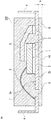
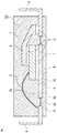
- FIG. 1 is a cross-sectional view showing the configuration of the semiconductor device according to the first embodiment.
- the semiconductor device 100 includes a semiconductor element 1, a lead frame 2, external terminals 4, wires 5, inner leads 6, a first insulating resin portion 7, and a second insulating resin portion. 8 is provided.
- a semiconductor element 1 such as an IGBT, a MOSFET, an IC chip, or an LSI chip has a bonding member 3 made of solder, silver or the like on the upper surface (hereinafter referred to as a mounting surface 2a) of the lead frame 2 in the figure.
- the lead frame 2 is a copper plate, a copper alloy plate, or the like, and the surface of the lead frame 2 is coated with metal plating (not shown) such as gold, silver, nickel, or tin.
- the electrode pad of the semiconductor element 1 is electrically connected to the external terminal 4 via the wire 5 connected by wire bonding, or the inner lead 6 made of a material such as a copper plate or a copper alloy plate.
- the element 1 inputs and outputs signals to and from an external device via the external terminal 4.
- the wire 5 and the inner lead 6 can be replaced with each other.
- the wire 5 is made of gold, silver, aluminum, copper or the like, and the wire diameter is about 20 ⁇ m to 500 ⁇ m.
- the lead frame 2 has a first insulating resin portion 7 made of a first insulating resin on the mounting surface 2a side.
- a second insulating resin portion 8 made of a second insulating resin is formed on the heat radiating surface 2b side, which is the surface opposite to the mounting surface 2a of the lead frame 2.
- the first insulating resin portion 7 is filled with a space between two spaced apart regions of the lead frame 2 (hereinafter referred to as “die pad space 9”). Yes.
- the second insulating resin portion 8 has a thin molded portion 10 formed in contact with the heat radiating surface 2 b of the lead frame 2.
- the thin molded portion 10 has a thickness H of about 0.022 mm to 0.15 mm and is formed of the second insulating resin.
- the thin molded portion 10 is joined to a heat sink (not shown) made of copper, aluminum or the like via a heat radiating member such as grease.
- the resin that forms the first insulating resin portion 7 and the second insulating resin portion 8 is a thermosetting epoxy resin or the like. However, a resin having higher thermal conductivity than the first insulating resin portion 7 on the mounting surface 2a side is used for the second insulating resin portion 8 on the heat radiating surface 2b side of the lead frame 2. As will be described later, the second insulating resin forming the second insulating resin portion 8 contains a filler 18 such as silica, alumina, boron nitride, or aluminum nitride having good thermal conductivity. The thermal conductivity of the second insulating resin portion 8 is 3 W / m ⁇ K to 12 W / m ⁇ K.
- a low-stress resin with good fluidity used for a general semiconductor device is used.
- a low stress resin in which silicone is added to a thermosetting epoxy resin or the like, or a low stress resin having a thermal expansion coefficient close to that of a lead frame is used.
- FIG. 2 is a flowchart showing a manufacturing process of the semiconductor device 100 of the first embodiment.
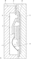
- FIG. 3 is a cross-sectional view of the resin molding machine 11 for forming the powdery second insulating resin 8a on the sheet-shaped second insulating resin 8b having a desired shape. A flange 13 that is compressed into the insulating resin 8b is also shown.
- FIG. 4 is a cross-sectional view of the resin molding machine 11 showing that the powdery second insulating resin 8a is compressed by the flange 13 and formed on the sheet-like second insulating resin 8b.
- FIG. 3 is a cross-sectional view of the resin molding machine 11 for forming the powdery second insulating resin 8a on the sheet-shaped second insulating resin 8b having a desired shape. A flange 13 that is compressed into the insulating resin 8b is also shown.
- FIG. 4 is a cross-sectional view of the resin molding machine 11 showing that the powdery second insulating resin 8a is compressed by the
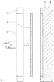
- FIG. 5 is a cross-sectional view showing a state in which the sheet-like second insulating resin 8b on the resin molding machine 11 is pushed out to the flange 13 and dropped into the lower mold cavity 15 of the lower mold 14 of the transfer mold.
- FIG. FIG. 6 is a cross-sectional view in which the sheet-like second insulating resin 8 b and the lead frame 2 on which the semiconductor element 1 is mounted are arranged in the lower mold 14.
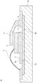
- FIG. 7 is a cross-sectional view showing the transfer molding in which the lead frame 2 on which the sheet-like second insulating resin 8b and the semiconductor element 1 are mounted is arranged on the transfer molding die.
- FIG. 3 and FIG. 4 are diagrams for explaining the “step of forming a powdery second insulating resin into a sheet-like second insulating resin with a resin molding device” in step S10 of FIG.
- the resin molding machine 11 is for forming the powdery second insulating resin 8 a on the sheet-like second insulating resin 8 b, and includes a base portion 12. Then, the powdery second insulating resin 8 a is spread on the base portion 12 of the resin molding machine 11.
- the ridge 13 descends toward the powdery second insulating resin 8a sprayed on the base portion 12, and the powdery second insulating resin 8a is compression-molded into a sheet-shaped second insulating resin 8b having a desired shape. . After that, when the powdery second insulating resin 8a is compressed by the ridge 13 to be formed into the sheet-like second insulating resin 8b, the ridge 13 once rises as shown in FIG.
- FIG. 5 is a diagram for explaining the “step of transporting the sheet-like second insulating resin to the upper part of the lower mold in a state where it is arranged in the resin molder and arranging it in the lower mold” in step S11 of FIG.
- the sheet-like second insulating resin 8 b is conveyed to the upper part of the lower mold 14 of the transfer molding die while being placed in the resin molding machine 11.
- the lower base portion 12 of the sheet-like second insulating resin 8b is removed, and the collar 13 is lowered again, whereby the sheet-like second insulating resin 8b. Is fitted into the lower mold cavity 15.
- FIG. 6 is a diagram for explaining the “step of arranging the lead frame on which the semiconductor element is mounted on the sheet-like second insulating resin arranged in the lower mold” in step S12 of FIG.
- the semiconductor element 1 is placed on the sheet-like second insulating resin 8 b arranged in the lower mold 14 so that the second insulating resin 8 b and the heat radiating surface 2 b of the lead frame 2 face each other.
- the mounted lead frame 2 is installed in the lower mold 14. At this time, the sheet-like second insulating resin 8b and the lead frame 2 may or may not contact each other.
- FIG. 7 is a diagram for explaining the “step of performing transfer molding by installing the upper mold in the lower mold” in step S13 of FIG.
- the upper mold 16 of the transfer mold is installed, and transfer molding is performed.
- the first insulating resin 7 a is melted by heat and pressure applied by the lower mold 14 and the upper mold 16 of transfer molding, injected through the gate into the upper mold cavity 17, and then applied to the mounting surface 2 a of the lead frame 2.
- One insulating resin portion 7 is formed.
- the sheet-like second insulating resin 8b is melted by the heat and pressure applied by the lower mold 14 and the upper mold 16, and is brought into close contact with the lead frame 2 and the first insulating resin 7a so as to dissipate heat from the lead frame 2.
- a second insulating resin portion 8 is formed on 2b.
- the first insulating resin 7a and the sheet-like second insulating resin 8b are simultaneously melted, two kinds of resins are mixed at the contact portion.
- the first insulating resin portion 7 and the first insulating resin 7b are mixed.
- a mixed layer in which the resins are mixed is formed at the interface with the insulating resin portion 8.
- the first insulating resin portion 7 and the second insulating resin portion 8 are formed on the mounting surface 2a and the heat radiating surface 2b of the lead frame 2 by one transfer molding, and the transfer molding process is completed.
- FIG. 8 is an enlarged cross-sectional view showing the thin molded portion 10 of the semiconductor device 100 after transfer molding.
- an insulating resin such as an epoxy resin containing a thermally conductive filler 18 such as silica, alumina, boron nitride, aluminum nitride is used. ing.
- the maximum filler diameter (filler cut point) of the filler 18 is 0.02 mm to 0.75 mm, and the thickness H of the thin molded portion 10 after transfer molding is 1.1 to 2 times the maximum filler diameter. 0.022 mm to 0.15 mm.
- the powdery second insulating resin is molded into the sheet-like second insulating resin by the resin molding machine, and the sheet-like second insulating resin is arranged in the resin molding machine. Then, it is transported to the upper part of the lower mold and placed in the lower mold, a lead frame mounted with a semiconductor element is placed on the sheet-like second insulating resin placed in the lower mold, and the upper mold is placed in the lower mold. A mold is installed and transfer molding is performed.
- the thickness of the sheet-like second insulating resin is as thin as 0.022 mm to 0.15 mm and low in rigidity.
- the sheet-like second insulating resin is conveyed to the lower mold while being placed in the resin molding machine, Can be prevented.
- a metal plate such as a copper foil. improves.
- chipping or cracking during manufacture and transportation of the sheet-like second insulating resin, it is transported to the lower mold in a state of being placed in the resin molding machine, so that a thin molded part is formed. The required volume is placed in the lower mold.
- the sheet-like second insulating resin melts and flows, chipping or cracking can be compensated for by the resin flow, so that the product does not become defective and productivity is improved.
- the first insulating resin is formed on the mounting surface of the lead frame by the transfer molding process with the sheet-like second insulating resin disposed on the heat dissipation surface of the lead frame, the flow of the sheet-like second insulating resin This improves the wettability of the lead frame and improves the adhesion between the thin molded portion and the lead frame.
- first insulating resin and the sheet-like second insulating resin melt at the same time, a mixed layer is formed in which the resins are mixed at the interface between the first insulating resin portion and the second insulating resin portion.
- the adhesion between the part and the second insulating resin part is improved.
- the adhesiveness between the first insulating resin part and the second insulating resin part is improved, the adhesiveness between the lead frame and the second insulating resin part is improved, and peeling or chipping of the thin molded part is less likely to occur. Therefore, it is possible to obtain a highly reliable semiconductor device that is inexpensive, high in productivity, excellent in heat dissipation and insulation.
- the surface of the lead frame 2 is coated with a metal plating such as gold, silver, nickel, or tin, but may not be coated.
- a metal plating such as gold, silver, nickel, or tin
- the lead frame 2 having a uniform thickness is used.
- a lead frame having a partially different thickness may be used.
- the heat sink is joined to the thin molded portion 10 via a heat radiating member such as grease, but the heat radiating member may not be used.
- the first insulating resin portion 7 on the mounting surface 2a side may have the same heat dissipation.
- the first insulating resin portion 7 may be a high thermal conductive resin having a thermal conductivity of 3 W / m ⁇ K to 12 W / m ⁇ K, similar to the second insulating resin portion 8.
- FIG. FIG. 9 is a cross-sectional view showing the configuration of the semiconductor device according to the second embodiment of the present invention.
- the semiconductor device 101 according to the second embodiment is a modification of the semiconductor device 100 according to the first embodiment, and since the overall configuration is the same, differences from the first embodiment will be described.
- the space between the die pads 9 of the lead frame 2 is filled with the first insulating resin to form a part of the first insulating resin portion 7.
- the semiconductor device 101 according to the second embodiment among the inter-die pads 9 of the lead frame 2, at least a part of the inter-die pads 9 includes the inter-lead frame filling portion 8d formed of the second insulating resin. Is formed. That is, in the second embodiment, the second insulating resin portion 8 includes the lead frame filling portion 8d and the thin molded portion 10.
- the inter-lead-frame filling portion 8d When the inter-lead-frame filling portion 8d is in close contact with the side surface of the lead frame 2, the area where the second insulating resin portion 8 and the lead frame 2 are in close contact with each other increases. As a result, the thin molded portion 10 and the lead frame 2 are in close contact with each other. Improves.
- the second insulating resin portion 8 is partially thickened by having the inter-lead frame filling portion 8d, the strength of the thin molded portion 10 is improved and chipping and cracking are less likely to occur. Furthermore, there is an effect that heat dissipation is improved by increasing an area where the lead frame 2 serving as a heat dissipation path and the second insulating resin portion 8 having high thermal conductivity are in close contact with each other. Furthermore, in the second embodiment, the entire side surface of the lead frame 2 is covered with the high thermal conductivity second insulating resin portion 8 to further improve the heat dissipation.
- an uneven portion in particular, a burred portion 19 may be formed on a part of the side surface of the lead frame 2 on which the inter-lead frame filling portion 8d is arranged.
- the concave and convex portions, particularly the burrs 19 by pressing on the side surfaces of the lead frame 2, the adhesion between the lead frame 2 and the inter-lead frame filling portion 8d is further improved by the anchor effect.
- the semiconductor device 101 according to the second embodiment is manufactured by a manufacturing method having a transfer molding process similar to that of the first embodiment.
- the second insulating resin used for the second insulating resin portion 8 is a resin having a lower viscosity when melted and better fluidity than the second insulating resin of the first embodiment.
- the pressure during transfer molding is 8 to 20 MPa
- the mold temperature is 165 to 180 degrees
- the minimum viscosity of the first insulating resin and the second insulating resin is 10 to 100 Pa ⁇ s.
- the first insulating resin 7a and the sheet-like second insulating resin 8b are simultaneously melted, and part or all of the second insulating resin is interposed between the die pads 9 of the lead frame 2.
- the lead frame filling portion 8d and the thin molded portion 10 are formed.
- the inter-lead frame filling portion integrally formed with the thin molded portion between at least some of the die pads of the lead frame.
- the adhesion between the thin molded part and the lead frame is improved.
- an uneven portion, particularly a burr portion, on the side surface of the lead frame where the inter-lead frame filling portion is disposed the adhesion is further improved by the anchor effect.
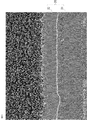
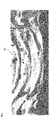
- FIG. FIG. 11 is a scanning electron micrograph showing the surface state of the lead frame of the semiconductor device according to the third embodiment of the present invention. Note that the overall configuration of the semiconductor device according to the third embodiment is the same as that of the first embodiment or the second embodiment, and therefore, only differences from the first embodiment or the second embodiment will be described. To do.
- the method for manufacturing the semiconductor device according to the third embodiment is the same as that in the first embodiment, and a description thereof will be omitted.
- the semiconductor device uses a rough metal plating lead frame 20 instead of the lead frame 2 used in the first embodiment.
- the rough metal plating lead frame 20 is a surface of a lead frame 21 made of copper or a copper alloy by rough metal plating 22 of nickel, tin, silver, gold or the like having a surface roughness Ra of about 0.06 to 0.2. It is a coating.
- the anchor effect of the rough metal plating makes it possible to The adhesion between the first insulating resin portion and the second insulating resin portion is improved. Furthermore, since the rough metal plating lead frame has a larger surface area than a normal lead frame, heat dissipation is improved.
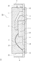
- FIG. FIG. 12 is a cross-sectional view showing the configuration of the semiconductor device according to the fourth embodiment of the present invention.
- the semiconductor device 102 according to the fourth embodiment has the same overall configuration as that of the semiconductor device according to the first embodiment or the second embodiment, and thus differs from the first embodiment or the second embodiment. Only the point will be described.
- the method for manufacturing the semiconductor device 102 according to the fourth embodiment is the same as that in the first embodiment, and a description thereof will be omitted.
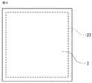
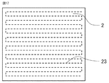
- the lead frame 2 of the semiconductor device 102 is coated with metal plating (not shown), and includes a scale-like portion 23 obtained by deforming the surface of the metal plating into a scale shape.
- the scale portions 23 are disposed on the outer peripheral portions of the mounting surface 2 a and the heat radiating surface 2 b of the lead frame 2. Due to the anchor effect of the scale-like portion 23, the first insulating resin portion 7 and the second insulating resin portion 8 are prevented from peeling from the lead frame 2.
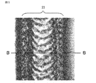
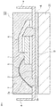
- FIG. 13 and FIG. 14 are diagrams by scanning electron micrographs showing the form of the scale-like portion 23.
- 13 is a scanning electron micrograph from the top
- FIG. 14 is a top perspective view of a cross section taken along line BB in FIG.
- the scaly portion 23 is obtained by melting the metal plating that coats the lead frame 2 by, for example, continuously performing spot irradiation with a laser and deforming it into a scaly shape.
- the scaly portion 23 is continuously provided with scaly projections, and both sides thereof are raised.
- the scale portion 23 is formed by laser irradiation, the scale portion 23 can be disposed at an arbitrary position of the lead frame 2. For example, when the semiconductor device is discharged from the molding die or when stress is applied at the time of gate break and initial peeling is likely to occur, or where the adhesion with the first insulating resin portion 7 or the second insulating resin portion 8 is low, It can be selectively arranged. Further, the width and height of the scale-like portion 23 can be adjusted by the output of the laser, the scanning speed, and the like. The width of the scale-like portion 23 (the width indicated by the scale-like portion 23 in FIG. 13) is desirably 60 ⁇ m or more, and the adhesiveness is further improved by increasing the width in accordance with the area of the place to be arranged.
- each figure is the figure which looked at the lead frame 2 from the upper surface, and the upper surface shape of the lead frame 2 is made into the rectangle for simplification.
- at least one of the first insulating resin portion 7 and the second insulating resin portion 8 is a gate break that is a trace of resin remaining in the gate of the molding die used in the transfer molding process. It has a trace 24.
- the scaly portion 23 is disposed on the surface of the lead frame 2 close to the gate break mark 24. Thereby, the contact
- the scale portion 23 is disposed on at least one outer peripheral portion of the mounting surface 2a and the heat radiation surface 2b of the lead frame 2.
- the scale portion 23 is arranged on at least one of the mounting surface 2a and the heat radiating surface 2b of the lead frame 2. Thereby, it becomes possible to suppress peeling over the entire surface.
- the lead frame and the first insulating resin portion or the second insulating resin portion can be obtained by providing a scale-like portion at an arbitrary position of the lead frame. Adhesion with the two insulating resin parts is improved.
- FIG. FIG. 18 is a sectional view showing a semiconductor device according to the fifth embodiment of the present invention
- FIGS. 19 to 21 are sectional views showing a method for manufacturing the semiconductor device according to the fifth embodiment.
- the semiconductor device 103 according to the fifth embodiment has the same overall configuration as the semiconductor devices according to the first to fourth embodiments, and therefore differs from the first to fourth embodiments. I will explain only.
- the heat sink 25 is installed on the surface opposite to the heat radiating surface 2 b of the lead frame 2 of the thin molded portion 10.
- the resin molding machine 11A is for forming the powdery second insulating resin 8a on the sheet-like second insulating resin 8b, and includes a base portion 12A.
- the heat sink 25 is arrange
- the flange 13A descends toward the powdery second insulating resin 8a, and the powdery second insulating resin 8a is compression-molded into a sheet-shaped second insulating resin 8b having a desired shape. Thereafter, the kite 13A rises once.
- the sheet-like second insulating resin 8b is conveyed to the upper part of the lower mold 14A of the transfer mold while being placed on the heat sink 25 of the resin molding machine 11A. Then, when reaching the upper portion of the lower mold cavity 15A of the lower mold 14A, the base portion 12A at the lower portion of the heat sink 25 is removed, and the collar 13A is lowered again, so that the sheet-like second insulating resin 8b and the heat sink 25 are It is inserted into the mold cavity 15A.
- the second insulating resin 8b and the heat radiation surface 2b of the lead frame 2 face each other on the sheet-like second insulating resin 8b and the heat sink 25 arranged in the lower mold 14A.
- the lead frame 2 on which the semiconductor element 1 is mounted is placed on the lower mold 14A.
- the upper mold 16A of the transfer mold is placed in a state where the lead frame 2 on which the sheet-like second insulating resin 8b, the heat sink 25, and the semiconductor element 1 are mounted is placed on the lower mold 14A, and transfer molding is performed.
- the first insulating resin 7a is melted by heat and pressure applied by the lower mold 14A and the upper mold 16A of transfer molding, injected through the gate into the upper mold cavity 17A, and is then applied to the mounting surface 2a of the lead frame 2 on the mounting surface 2a.
- One insulating resin portion 7 is formed.
- the sheet-like second insulating resin 8b is melted by heat and pressure applied by the lower mold 14 and the upper mold 16, and the second insulating resin portion 8 is formed on the heat radiation surface 2b of the lead frame 2, A heat sink 25 is joined to the thin molded portion 10.
- a heat radiating member such as grease for adhering the heat sink 25 becomes unnecessary.
- the thin molded part 10 is directly joined to the heat sink 25, so that the heat dissipation is further improved. Further, after the transfer molding step, the step of joining the heat sink 25 to the thin molded portion 10 via a heat radiating member such as grease can be omitted.
- a heat sink 25 ⁇ / b> A having a smaller joint area than the heat radiation side area of the thin molded portion 10 may be installed on the surface opposite to the heat radiation surface 2 b of the lead frame 2 of the thin molded portion 10.
- the creepage distance can be increased according to the dielectric strength performance of the semiconductor element 1 and the processing accuracy of the heat sink 25A.
- FIG. FIG. 23 is a sectional view showing a semiconductor device according to the sixth embodiment of the present invention.
- the semiconductor device 105 according to the fifth embodiment has the same overall configuration as the semiconductor devices according to the first to fifth embodiments, and therefore differs from the first to fifth embodiments. I will explain only.
- the second insulating resin portion 8 is formed on the heat radiating surface 2b of the lead frame 2, and the outer peripheral end portion of the second insulating resin portion 8 has a frame shape with a thickness of about 0.15 mm to 2 mm.
- the skirt part 26 which is a projection part is provided.
- a thin molded portion 10 having a thickness of about 0.022 mm to 0.15 mm is integrally formed with the skirt portion 26.
- the thin molded portion 10 is joined to a heat sink (not shown) made of copper or aluminum via a heat radiating member such as grease.
- the skirt portion 26 that is a frame-like protrusion at the outer peripheral end portion of the second insulating resin portion 8
- the strength of the outer peripheral end portion of the lead frame 2 that is stressed during gate break is increased. Can be secured. Further, the creepage distance is increased and the insulation is improved, which is advantageous for a high-voltage module using an IGBT as the semiconductor element 1.
- the cross-sectional shape of the skirt portion 26 cut in the orthogonal direction is a rectangle, a square, a trapezoid, or the like.
- FIG. FIG. 24 is a cross-sectional view showing a semiconductor device according to Embodiment 7 of the present invention.
- the semiconductor device 106 according to the fifth embodiment is a modification of the semiconductor device according to the first to sixth embodiments, and differences from the first to sixth embodiments will be described.
- the first insulating resin portion 7 is formed on the mounting surface 2a of the lead frame 2 and the second insulating resin portion 8 is formed on the heat radiating surface 2b.
- the second insulating resin portion 8B is also formed on the mounting surface 2a side of the lead frame 2 to provide a heat radiating portion. That is, in the semiconductor device 106 according to the seventh embodiment, the second insulating resin portion 8B is formed on the surface of the first insulating resin portion 7 that faces the mounting surface 2a on which the semiconductor element 1 of the lead frame 2 is mounted.
- the heat sink 25B is arranged on the second insulating resin portion 8B.
- the seventh embodiment by providing the first insulating resin portion 7 on the mounting surface 2a side of the lead frame 2 with heat dissipation, high heat conduction around the semiconductor element 1 that is a heat-generating component. Since it can seal with resin and it is thermally radiated from the perimeter of the semiconductor element 1, heat dissipation improves.
- the resin molding machine 11 may be incorporated in a molding facility that can be transfer molded using a molding die, or may be a separate facility.
- the surface of the lead frame 2 is subjected to ultraviolet (UV) treatment before the transfer molding process in order to improve the adhesion of the first insulating resin portion 7 and the second insulating resin portion 8 to the lead frame 2.
- UV ultraviolet
- plasma treatment may be performed.
- the shape, number, and arrangement of each component of the semiconductor device according to each of the above-described embodiments for example, the semiconductor element 1, the external terminal 4, the wire 5, and the inner lead 6 are not particularly limited. It is appropriately selected according to the required function of the apparatus. Further, within the scope of the invention, the present invention can be freely combined with each other, or can be appropriately modified or omitted.
Abstract
Description
しかしながら、樹脂シートを製造および搬送する中で、樹脂シートの欠けまたは割れを防止するために剛性を高める必要があり、樹脂シートとしてある程度の厚みが必要となる。特に、樹脂シートに熱伝導性の良好なフィラーを含ませる場合は、樹脂シートの厚みはフィラーの最大径の3倍程度の厚みが必要となっていた。また、樹脂シートを搬送または取り扱いを行う上で剛性を高めるため、銅箔等の金属板に樹脂シートを貼り付ける必要があった。 In
However, in manufacturing and transporting the resin sheet, it is necessary to increase rigidity in order to prevent chipping or cracking of the resin sheet, and a certain thickness is required as the resin sheet. In particular, when the resin sheet contains a filler with good thermal conductivity, the thickness of the resin sheet needs to be about three times the maximum diameter of the filler. Moreover, in order to improve rigidity in conveying or handling the resin sheet, it is necessary to attach the resin sheet to a metal plate such as a copper foil.
半導体素子が実装されたリードフレーム、前記リードフレームの前記半導体素子が実装された面である実装面を封止する第一絶縁樹脂部、前記リードフレームの前記実装面と反対側の面である放熱面を封止する第二絶縁樹脂部を備え、
前記第二絶縁樹脂部は、最大径が0.02mm~0.075mmのフィラーを含有し、
前記第二絶縁樹脂部は、前記リードフレームの前記放熱面に接して形成される薄肉成形部を有し、前記薄肉成形部の厚さが、前記フィラーの最大径の1.1~2倍であり、
前記第一絶縁樹脂部と前記第二絶縁樹脂部の界面で互いの樹脂が混合されている混合層を有するものである。 A semiconductor device according to the present invention includes:
A lead frame on which a semiconductor element is mounted, a first insulating resin portion that seals a mounting surface that is a surface on which the semiconductor element is mounted on the lead frame, and a heat dissipation that is a surface opposite to the mounting surface on the lead frame A second insulating resin part for sealing the surface;
The second insulating resin portion contains a filler having a maximum diameter of 0.02 mm to 0.075 mm,
The second insulating resin portion has a thin molded portion formed in contact with the heat radiating surface of the lead frame, and the thickness of the thin molded portion is 1.1 to 2 times the maximum diameter of the filler. Yes,
It has a mixed layer in which the respective resins are mixed at the interface between the first insulating resin portion and the second insulating resin portion.
樹脂成形器によりパウダー状第二絶縁樹脂をシート状第二絶縁樹脂に成形する工程と、
前記シート状第二絶縁樹脂を前記樹脂成形器に配置された状態で下金型の上部に搬送して前記下金型に配置する工程と、
前記下金型に配置された前記シート状第二絶縁樹脂の上に半導体素子を実装したリードフレームを配置する工程と、
前記下金型に上金型を設置して、トランスファー成形を行い、前記リードフレームの前記半導体素子が実装された面である実装面を封止する第一絶縁樹脂部、および前記リードフレームの前記実装面と反対側の面である放熱面を封止する第二絶縁樹脂部を形成する工程を備えたものである。 A method for manufacturing a semiconductor device according to the present invention includes:
Forming a powdery second insulating resin into a sheet-like second insulating resin with a resin molding device;
Transporting the sheet-like second insulating resin to the upper part of the lower mold in a state of being placed in the resin molding machine, and placing it on the lower mold;
Arranging a lead frame on which a semiconductor element is mounted on the sheet-like second insulating resin arranged in the lower mold;
An upper mold is placed on the lower mold, transfer molding is performed, and a first insulating resin portion that seals a mounting surface, which is a surface on which the semiconductor element is mounted, of the lead frame, and the lead frame The method includes a step of forming a second insulating resin portion that seals the heat dissipating surface that is the surface opposite to the mounting surface.
樹脂成形器によりヒートシンクの上でパウダー状第二絶縁樹脂をシート状第二絶縁樹脂に成形する工程と、
前記ヒートシンクの上で成形された前記シート状第二絶縁樹脂を前記ヒートシンクとともに前記樹脂成形器に配置された状態で下金型の上部に搬送して前記下金型に配置する工程と、
前記下金型に配置された前記ヒートシンクおよび前記シート状第二絶縁樹脂の上に半導体素子を実装したリードフレームを配置する工程と、
前記下金型に上金型を設置して、トランスファー成形を行い、前記リードフレームの前記半導体素子が実装された面である実装面を封止する第一絶縁樹脂部、および前記リードフレームの前記実装面と反対側の面である放熱面を封止する第二絶縁樹脂部を形成するとともに、前記第二絶縁樹脂部に前記ヒートシンクを接合する工程を備えたものである。 A method for manufacturing a semiconductor device according to the present invention includes:
Forming a powdery second insulating resin into a sheet-like second insulating resin on a heat sink by a resin molding machine;
Conveying the sheet-like second insulating resin molded on the heat sink together with the heat sink to the upper part of the lower mold in a state of being arranged on the resin molder;
Arranging a lead frame on which a semiconductor element is mounted on the heat sink and the sheet-like second insulating resin arranged in the lower mold; and
An upper mold is placed on the lower mold, transfer molding is performed, and a first insulating resin portion that seals a mounting surface, which is a surface on which the semiconductor element is mounted, of the lead frame, and the lead frame A step of forming a second insulating resin portion for sealing a heat radiating surface that is a surface opposite to the mounting surface and joining the heat sink to the second insulating resin portion are provided.
以下、この発明の実施の形態1に係る半導体装置について、図面に基づいて説明する。図1は、本実施の形態1に係る半導体装置の構成を示す断面図である。
A semiconductor device according to
図2は、実施の形態1の半導体装置100の製造工程を示すフローチャートである。図3は、パウダー状第二絶縁樹脂8aを所望の形状のシート状第二絶縁樹脂8bに形成するための樹脂成形器11の断面図であり、パウダー状第二絶縁樹脂8aをシート状第二絶縁樹脂8bに圧縮する杵13も併せて示している。図4は、パウダー状第二絶縁樹脂8aが杵13で圧縮され、シート状第二絶縁樹脂8bに形成されたところを示す樹脂成形器11の断面図である。図5は、樹脂成形器11上のシート状第二絶縁樹脂8bが杵13に押し出されて、トランスファー成形金型の下金型14の下型キャビティ15へ落とされてはめ込まれる様子を示した断面図である。図6は、シート状第二絶縁樹脂8bと半導体素子1が実装されたリードフレーム2とを下金型14に配置した断面図である。図7は、トランスファー成形金型にシート状第二絶縁樹脂8bと半導体素子1が実装されたリードフレーム2を配置し、トランスファー成形を行うところを示す断面図である。 Next, a method for manufacturing the semiconductor device according to the first embodiment will be described with reference to FIGS.
FIG. 2 is a flowchart showing a manufacturing process of the
図3および図4は、図2のステップS10の「樹脂成形器によりパウダー状第二絶縁樹脂をシート状第二絶縁樹脂に成形する工程」を説明する図である。図3において、樹脂成形器11は、パウダー状第二絶縁樹脂8aをシート状第二絶縁樹脂8bに形成するためのものであり、基底部12を備えている。そして、樹脂成形器11の基底部12上にパウダー状第二絶縁樹脂8aが散布される。その後、杵13が、基底部12上に散布されたパウダー状第二絶縁樹脂8aへ向かって下降し、パウダー状第二絶縁樹脂8aを所望の形状のシート状第二絶縁樹脂8bに圧縮成形する。その後、杵13によりパウダー状第二絶縁樹脂8aが圧縮されてシート状第二絶縁樹脂8bに形成されると、図4に示すように杵13は一旦上昇する。 The method for manufacturing the
FIG. 3 and FIG. 4 are diagrams for explaining the “step of forming a powdery second insulating resin into a sheet-like second insulating resin with a resin molding device” in step S10 of FIG. In FIG. 3, the
図9は、本発明の実施の形態2に係る半導体装置の構成を示す断面図である。本実施の形態2に係る半導体装置101は、上記実施の形態1に係る半導体装置100の変形例であり、全体的な構成は同様であるため、実施の形態1との相違点について説明する。
FIG. 9 is a cross-sectional view showing the configuration of the semiconductor device according to the second embodiment of the present invention. The
図11は、本発明の実施の形態3に係る半導体装置のリードフレームの表面状態を示す走査電子顕微鏡写真による図である。なお、本実施の形態3に係る半導体装置の全体的な構成は、上記実施の形態1又は実施の形態2と同様であるので、実施の形態1又は実施の形態2との相違点のみを説明する。また、本実施の形態3に係る半導体装置の製造方法は、上記実施の形態1と同様であるので説明を省略する。
FIG. 11 is a scanning electron micrograph showing the surface state of the lead frame of the semiconductor device according to the third embodiment of the present invention. Note that the overall configuration of the semiconductor device according to the third embodiment is the same as that of the first embodiment or the second embodiment, and therefore, only differences from the first embodiment or the second embodiment will be described. To do. The method for manufacturing the semiconductor device according to the third embodiment is the same as that in the first embodiment, and a description thereof will be omitted.
図12は、本発明の実施の形態4に係る半導体装置の構成を示す断面図である。本実施の形態4に係る半導体装置102は、上記実施の形態1または実施の形態2に係る半導体装置と全体的な構成は同様であるので、上記実施の形態1または実施の形態2との相違点のみを説明する。また、本実施の形態4に係る半導体装置102の製造方法は、上記実施の形態1と同様であるので説明を省略する。
FIG. 12 is a cross-sectional view showing the configuration of the semiconductor device according to the fourth embodiment of the present invention. The
まず、図15に示す例は、第一絶縁樹脂部7および第二絶縁樹脂部8の少なくとも一方は、トランスファー成形工程で用いられた成形金型のゲート内に残った樹脂の痕跡であるゲートブレイク跡24を有している。そして、鱗状部23は、ゲートブレイク跡24に近接したリードフレーム2の表面に配置されている。
これにより、初期的な剥離が生じやすいゲートブレイク跡24に近接したリードフレーム2と第一絶縁樹脂部7又は第二絶縁樹脂部8との密着力を向上させることができる。 An example of the arrangement of the
First, in the example shown in FIG. 15, at least one of the first insulating
Thereby, the contact | adhesion power of the
図18は、本発明の実施の形態5に係る半導体装置を示す断面図、図19~図21は、本実施の形態5に係る半導体装置の製造方法を示す断面図である。本実施の形態5に係る半導体装置103は、上記実施の形態1~実施の形態4の半導体装置と全体的な構成は同様であるため、上記実施の形態1~実施の形態4との相違点のみを説明する。
FIG. 18 is a sectional view showing a semiconductor device according to the fifth embodiment of the present invention, and FIGS. 19 to 21 are sectional views showing a method for manufacturing the semiconductor device according to the fifth embodiment. The
図19に示すように、樹脂成形器11Aは、パウダー状第二絶縁樹脂8aをシート状第二絶縁樹脂8bに形成するためのものであり、基底部12Aを備えている。そして、樹脂成形器11Aの基底部12A上にヒートシンク25が配置され、その上にパウダー状第二絶縁樹脂8aが散布される。その後、杵13Aが、パウダー状第二絶縁樹脂8aへ向かって下降し、パウダー状第二絶縁樹脂8aを所望の形状のシート状第二絶縁樹脂8bに圧縮成形する。その後、杵13Aは一旦上昇する。 In the
As shown in FIG. 19, the
図23は、本発明の実施の形態6に係る半導体装置を示す断面図である。本実施の形態5に係る半導体装置105は、上記実施の形態1~実施の形態5の半導体装置と全体的な構成は同様であるため、上記実施の形態1~実施の形態5との相違点のみを説明する。
FIG. 23 is a sectional view showing a semiconductor device according to the sixth embodiment of the present invention. The
図24は、本発明の実施の形態7に係る半導体装置を示す断面図である。本実施の形態5に係る半導体装置106は、上記実施の形態1~実施の形態6に係る半導体装置の変形例であり、上記実施の形態1~実施の形態6との相違点について説明する。
FIG. 24 is a cross-sectional view showing a semiconductor device according to
また、本発明は、その発明の範囲内において、各実施の形態を自由に組み合わせたり、各実施の形態を適宜、変形、省略することが可能である。 Note that the shape, number, and arrangement of each component of the semiconductor device according to each of the above-described embodiments, for example, the
Further, within the scope of the invention, the present invention can be freely combined with each other, or can be appropriately modified or omitted.
Claims (17)
- 半導体素子が実装されたリードフレーム、前記リードフレームの前記半導体素子が実装された面である実装面を封止する第一絶縁樹脂部、前記リードフレームの前記実装面と反対側の面である放熱面を封止する第二絶縁樹脂部を備え、
前記第二絶縁樹脂部は、最大径が0.02mm~0.075mmのフィラーを含有し、
前記第二絶縁樹脂部は、前記リードフレームの前記放熱面に接して形成される薄肉成形部を有し、前記薄肉成形部の厚さが、前記フィラーの最大径の1.1~2倍であり、
前記第一絶縁樹脂部と前記第二絶縁樹脂部の界面で互いの樹脂が混合されている混合層を有する半導体装置。 A lead frame on which a semiconductor element is mounted, a first insulating resin portion that seals a mounting surface that is a surface on which the semiconductor element is mounted on the lead frame, and a heat dissipation that is a surface opposite to the mounting surface on the lead frame A second insulating resin part for sealing the surface;
The second insulating resin portion contains a filler having a maximum diameter of 0.02 mm to 0.075 mm,
The second insulating resin portion has a thin molded portion formed in contact with the heat radiating surface of the lead frame, and the thickness of the thin molded portion is 1.1 to 2 times the maximum diameter of the filler. Yes,
A semiconductor device having a mixed layer in which resins are mixed at an interface between the first insulating resin portion and the second insulating resin portion. - 前記リードフレームの離間された二つの領域の間の少なくとも一部に、前記第二絶縁樹脂部の一部であるリードフレーム間充填部が形成されている請求項1に記載の半導体装置。 2. The semiconductor device according to claim 1, wherein an inter-lead frame filling portion that is a part of the second insulating resin portion is formed at least at a part between two spaced apart regions of the lead frame.
- 前記リードフレーム間充填部が形成された前記リードフレームの側面に、凹凸部を有する請求項2に記載の半導体装置。 3. The semiconductor device according to claim 2, wherein an uneven portion is provided on a side surface of the lead frame in which the inter-lead frame filling portion is formed.
- 前記凹凸部は、カエリ部である請求項3に記載の半導体装置。 The semiconductor device according to claim 3, wherein the uneven portion is a burred portion.
- 前記リードフレームとして、その表面が粗化された金属めっきにより被膜された粗化金属めっきリードフレームを使用した請求項1から請求項4のいずれか1項に記載の半導体装置。 The semiconductor device according to any one of claims 1 to 4, wherein a rough metal plating lead frame whose surface is coated with a rough metal plating is used as the lead frame.
- 前記リードフレームは金属めっきにより被膜され、前記金属めっきの表面を鱗状に成形させた鱗状部を有する請求項1から請求項4のいずれか1項に記載の半導体装置。 5. The semiconductor device according to claim 1, wherein the lead frame is coated with metal plating and has a scaly portion obtained by forming the surface of the metal plating into a scaly shape. 6.
- 前記第一絶縁樹脂部および前記第二絶縁樹脂部の少なくとも一方は、ゲートブレイク跡を有し、前記鱗状部は、前記ゲートブレイク跡に対応する前記リードフレームの表面に配置されている請求項6に記載の半導体装置。 The at least one of the first insulating resin portion and the second insulating resin portion has a gate break mark, and the scale-like portion is disposed on the surface of the lead frame corresponding to the gate break mark. A semiconductor device according to 1.
- 前記鱗状部は、前記リードフレームの前記実装面および前記放熱面の少なくとも一方の外周部に配置されている請求項6に記載の半導体装置。 The semiconductor device according to claim 6, wherein the scale portion is disposed on an outer peripheral portion of at least one of the mounting surface and the heat dissipation surface of the lead frame.
- 前記鱗状部は、前記リードフレームの前記実装面および前記放熱面の少なくとも一方の全面に配置されている請求項6に記載の半導体装置。 The semiconductor device according to claim 6, wherein the scale portion is disposed on at least one of the mounting surface and the heat dissipation surface of the lead frame.
- 前記第二絶縁樹脂部には、前記第一絶縁樹脂部よりも熱伝導率が高い樹脂が用いられる請求項1から請求項9のいずれか1項に記載の半導体装置。 10. The semiconductor device according to claim 1, wherein a resin having a higher thermal conductivity than that of the first insulating resin portion is used for the second insulating resin portion.
- 前記第二絶縁樹脂部には、熱伝導率が3W/m・K~12W/m・Kの絶縁樹脂が用いられる請求項1から請求項9のいずれか1項に記載の半導体装置。 10. The semiconductor device according to claim 1, wherein an insulating resin having a thermal conductivity of 3 W / m · K to 12 W / m · K is used for the second insulating resin portion.
- 前記第一絶縁樹脂部には、熱伝導率が3W/m・K~12W/m・Kの絶縁樹脂が用いられる請求項11に記載の半導体装置。 12. The semiconductor device according to claim 11, wherein an insulating resin having a thermal conductivity of 3 W / m · K to 12 W / m · K is used for the first insulating resin portion.
- 前記薄肉成形部の前記リードフレームの前記放熱面と対向する面と反対側の面に、前記薄肉成形部の放熱側面積より接合面積が小さなヒートシンクが接合されている請求項1から請求項12のいずれか1項に記載の半導体装置。 13. A heat sink having a bonding area smaller than a heat dissipation area of the thin molded portion is bonded to a surface of the thin molded portion opposite to a surface facing the heat dissipation surface of the lead frame. The semiconductor device according to any one of the above.
- 前記第二絶縁樹脂部の外周端部には枠状突起部が設けられ、前記枠状突起部の内側には前記薄肉成形部が一体的に形成されている請求項1から請求項13のいずれか1項に記載の半導体装置。 The frame-shaped projection part is provided in the outer peripheral edge part of said 2nd insulating resin part, The said thin molded part is integrally formed in the inner side of the said frame-shaped projection part. 2. The semiconductor device according to claim 1.
- 樹脂成形器によりパウダー状第二絶縁樹脂をシート状第二絶縁樹脂に成形する工程と、
前記シート状第二絶縁樹脂を前記樹脂成形器に配置された状態で下金型の上部に搬送して前記下金型に配置する工程と、
前記下金型に配置された前記シート状第二絶縁樹脂の上に半導体素子を実装したリードフレームを配置する工程と、
前記下金型に上金型を設置して、トランスファー成形を行い、前記リードフレームの前記半導体素子が実装された面である実装面を封止する第一絶縁樹脂部、および前記リードフレームの前記実装面と反対側の面である放熱面を封止する第二絶縁樹脂部を形成する工程を備えた半導体装置の製造方法。 Forming a powdery second insulating resin into a sheet-like second insulating resin with a resin molding device;
Transporting the sheet-like second insulating resin to the upper part of the lower mold in a state of being placed in the resin molding machine, and placing it on the lower mold;
Arranging a lead frame on which a semiconductor element is mounted on the sheet-like second insulating resin arranged in the lower mold;
An upper mold is placed on the lower mold, transfer molding is performed, and a first insulating resin portion that seals a mounting surface, which is a surface on which the semiconductor element is mounted, of the lead frame, and the lead frame A method for manufacturing a semiconductor device, comprising a step of forming a second insulating resin portion that seals a heat dissipation surface that is a surface opposite to a mounting surface. - 樹脂成形器によりヒートシンクの上でパウダー状第二絶縁樹脂をシート状第二絶縁樹脂に成形する工程と、
前記ヒートシンクの上で成形された前記シート状第二絶縁樹脂を前記ヒートシンクとともに前記樹脂成形器に配置された状態で下金型の上部に搬送して前記下金型に配置する工程と、
前記下金型に配置された前記ヒートシンクおよび前記シート状第二絶縁樹脂の上に半導体素子を実装したリードフレームを配置する工程と、
前記下金型に上金型を設置して、トランスファー成形を行い、前記リードフレームの前記半導体素子が実装された面である実装面を封止する第一絶縁樹脂部、および前記リードフレームの前記実装面と反対側の面である放熱面を封止する第二絶縁樹脂部を形成するとともに、前記第二絶縁樹脂部に前記ヒートシンクを接合する工程を備えた半導体装置の製造方法。 Forming a powdery second insulating resin into a sheet-like second insulating resin on a heat sink by a resin molding machine;
Conveying the sheet-like second insulating resin molded on the heat sink together with the heat sink to the upper part of the lower mold in a state of being arranged on the resin molder;
Arranging a lead frame on which a semiconductor element is mounted on the heat sink and the sheet-like second insulating resin arranged in the lower mold; and
An upper mold is placed on the lower mold, transfer molding is performed, and a first insulating resin portion that seals a mounting surface, which is a surface on which the semiconductor element is mounted, of the lead frame, and the lead frame A method for manufacturing a semiconductor device, comprising: forming a second insulating resin portion that seals a heat radiating surface opposite to the mounting surface; and bonding the heat sink to the second insulating resin portion. - 前記リードフレームの前記実装面に前記半導体素子を実装する前に、前記リードフレームの表面に金属めっきを形成し、前記金属めっきにレーザー照射を行うことにより前記金属めっきの表面を鱗状に変形させた鱗状部を形成する工程を備えた請求項15または請求項16に記載の半導体装置の製造方法。 Before mounting the semiconductor element on the mounting surface of the lead frame, metal plating was formed on the surface of the lead frame, and the metal plating surface was deformed in a scale shape by performing laser irradiation on the metal plating. The method for manufacturing a semiconductor device according to claim 15, further comprising a step of forming a scaly portion.
Priority Applications (5)
| Application Number | Priority Date | Filing Date | Title |
|---|---|---|---|
| PCT/JP2016/056975 WO2017154072A1 (en) | 2016-03-07 | 2016-03-07 | Semiconductor device and method for manufacturing semiconductor device |
| US16/070,350 US11152275B2 (en) | 2016-03-07 | 2016-03-07 | Semiconductor device and method for manufacturing semiconductor device |
| CN201680083069.2A CN108701661A (en) | 2016-03-07 | 2016-03-07 | The manufacturing method of semiconductor device and semiconductor device |
| EP16893404.0A EP3428962B1 (en) | 2016-03-07 | 2016-03-07 | Semiconductor device and method for manufacturing semiconductor device |
| JP2018503866A JP6472568B2 (en) | 2016-03-07 | 2016-03-07 | Manufacturing method of semiconductor device |
Applications Claiming Priority (1)
| Application Number | Priority Date | Filing Date | Title |
|---|---|---|---|
| PCT/JP2016/056975 WO2017154072A1 (en) | 2016-03-07 | 2016-03-07 | Semiconductor device and method for manufacturing semiconductor device |
Publications (1)
| Publication Number | Publication Date |
|---|---|
| WO2017154072A1 true WO2017154072A1 (en) | 2017-09-14 |
Family
ID=59789124
Family Applications (1)
| Application Number | Title | Priority Date | Filing Date |
|---|---|---|---|
| PCT/JP2016/056975 WO2017154072A1 (en) | 2016-03-07 | 2016-03-07 | Semiconductor device and method for manufacturing semiconductor device |
Country Status (5)
| Country | Link |
|---|---|
| US (1) | US11152275B2 (en) |
| EP (1) | EP3428962B1 (en) |
| JP (1) | JP6472568B2 (en) |
| CN (1) | CN108701661A (en) |
| WO (1) | WO2017154072A1 (en) |
Cited By (1)
| Publication number | Priority date | Publication date | Assignee | Title |
|---|---|---|---|---|
| EP3848961A4 (en) * | 2018-09-06 | 2021-09-22 | Mitsubishi Electric Corporation | Semiconductor device |
Families Citing this family (1)
| Publication number | Priority date | Publication date | Assignee | Title |
|---|---|---|---|---|
| US20230260861A1 (en) * | 2022-02-11 | 2023-08-17 | Wolfspeed, Inc. | Semiconductor packages with increased power handling |
Citations (11)
| Publication number | Priority date | Publication date | Assignee | Title |
|---|---|---|---|---|
| JPH0215738U (en) * | 1988-07-15 | 1990-01-31 | ||
| JPH09102580A (en) * | 1995-08-02 | 1997-04-15 | Matsushita Electron Corp | Resin-sealed semiconductor device and fabrication thereof |
| JP2001170928A (en) * | 1999-12-22 | 2001-06-26 | Matsushita Electric Works Ltd | Molding material, electronic part and method for manufacturing molding material |
| JP2002237562A (en) * | 2001-02-09 | 2002-08-23 | Mitsubishi Electric Corp | Semiconductor device and method of manufacturing the same |
| JP2002299538A (en) * | 2001-03-30 | 2002-10-11 | Dainippon Printing Co Ltd | Lead frame and semiconductor package using the same |
| JP2009302526A (en) * | 2008-05-16 | 2009-12-24 | Denso Corp | Electronic circuit device and manufacturing method thereof |
| JP2011176024A (en) * | 2010-02-23 | 2011-09-08 | Mitsubishi Electric Corp | Thermosetting resin composition, b-stage heat conductive sheet, and power module |
| JP2012160517A (en) * | 2011-01-31 | 2012-08-23 | Mitsubishi Electric Corp | Manufacturing method of semiconductor device |
| WO2015151273A1 (en) * | 2014-04-04 | 2015-10-08 | 三菱電機株式会社 | Semiconductor device |
| JP2015191979A (en) * | 2014-03-27 | 2015-11-02 | デクセリアルズ株式会社 | Method for manufacturing thermally conductive sheet |
| JP2016018904A (en) * | 2014-07-09 | 2016-02-01 | 日産自動車株式会社 | Semiconductor device |
Family Cites Families (19)
| Publication number | Priority date | Publication date | Assignee | Title |
|---|---|---|---|---|
| JPH0927579A (en) | 1995-07-10 | 1997-01-28 | Apic Yamada Kk | Lead-frame manufacturing apparatus |
| JP3516789B2 (en) | 1995-11-15 | 2004-04-05 | 三菱電機株式会社 | Semiconductor power module |
| JP2000077435A (en) * | 1998-08-31 | 2000-03-14 | Hitachi Ltd | Semiconductor device and manufacture thereof |
| JP4220641B2 (en) | 2000-01-13 | 2009-02-04 | 電気化学工業株式会社 | Resin mold circuit board and electronic package |
| US6882048B2 (en) | 2001-03-30 | 2005-04-19 | Dainippon Printing Co., Ltd. | Lead frame and semiconductor package having a groove formed in the respective terminals for limiting a plating area |
| CN1321455C (en) * | 2001-04-13 | 2007-06-13 | 雅马哈株式会社 | Semiconductor device and packaging and its manufacturing method |
| JP2005109100A (en) | 2003-09-30 | 2005-04-21 | Mitsubishi Electric Corp | Semiconductor device and manufacturing method thereof |
| JP3854957B2 (en) | 2003-10-20 | 2006-12-06 | 三菱電機株式会社 | Semiconductor device manufacturing method and semiconductor device |
| JP2006222406A (en) | 2004-08-06 | 2006-08-24 | Denso Corp | Semiconductor device |
| DE102005043928B4 (en) * | 2004-09-16 | 2011-08-18 | Sharp Kk | Optical semiconductor device and method for its production |
| JP4463146B2 (en) | 2005-05-18 | 2010-05-12 | 三菱電機株式会社 | Manufacturing method of semiconductor device |
| JP2008187045A (en) * | 2007-01-30 | 2008-08-14 | Matsushita Electric Ind Co Ltd | Lead frame for semiconductor device, manufacturing method therefor, and the semiconductor device |
| CN101241890B (en) * | 2007-02-06 | 2012-05-23 | 百慕达南茂科技股份有限公司 | Chip package structure and its making method |
| JP4855329B2 (en) * | 2007-05-08 | 2012-01-18 | Towa株式会社 | Electronic component compression molding method and apparatus |
| JP2010109246A (en) * | 2008-10-31 | 2010-05-13 | Yaskawa Electric Corp | Semiconductor device, and method of manufacturing the same |
| US8044495B2 (en) * | 2009-06-22 | 2011-10-25 | Texas Instruments Incorporated | Metallic leadframes having laser-treated surfaces for improved adhesion to polymeric compounds |
| US20110140253A1 (en) | 2009-12-14 | 2011-06-16 | National Semiconductor Corporation | Dap ground bond enhancement |
| JP5563917B2 (en) * | 2010-07-22 | 2014-07-30 | セミコンダクター・コンポーネンツ・インダストリーズ・リミテッド・ライアビリティ・カンパニー | Circuit device and manufacturing method thereof |
| TWI490268B (en) * | 2011-03-28 | 2015-07-01 | Hitachi Chemical Co Ltd | Resin composition, resin sheet, cured resin sheet, resin sheet laminate, cured resin sheet laminate and method of producing the same, semiconductor device, and led device |
-
2016
- 2016-03-07 JP JP2018503866A patent/JP6472568B2/en active Active
- 2016-03-07 WO PCT/JP2016/056975 patent/WO2017154072A1/en active Application Filing
- 2016-03-07 EP EP16893404.0A patent/EP3428962B1/en active Active
- 2016-03-07 US US16/070,350 patent/US11152275B2/en active Active
- 2016-03-07 CN CN201680083069.2A patent/CN108701661A/en active Pending
Patent Citations (11)
| Publication number | Priority date | Publication date | Assignee | Title |
|---|---|---|---|---|
| JPH0215738U (en) * | 1988-07-15 | 1990-01-31 | ||
| JPH09102580A (en) * | 1995-08-02 | 1997-04-15 | Matsushita Electron Corp | Resin-sealed semiconductor device and fabrication thereof |
| JP2001170928A (en) * | 1999-12-22 | 2001-06-26 | Matsushita Electric Works Ltd | Molding material, electronic part and method for manufacturing molding material |
| JP2002237562A (en) * | 2001-02-09 | 2002-08-23 | Mitsubishi Electric Corp | Semiconductor device and method of manufacturing the same |
| JP2002299538A (en) * | 2001-03-30 | 2002-10-11 | Dainippon Printing Co Ltd | Lead frame and semiconductor package using the same |
| JP2009302526A (en) * | 2008-05-16 | 2009-12-24 | Denso Corp | Electronic circuit device and manufacturing method thereof |
| JP2011176024A (en) * | 2010-02-23 | 2011-09-08 | Mitsubishi Electric Corp | Thermosetting resin composition, b-stage heat conductive sheet, and power module |
| JP2012160517A (en) * | 2011-01-31 | 2012-08-23 | Mitsubishi Electric Corp | Manufacturing method of semiconductor device |
| JP2015191979A (en) * | 2014-03-27 | 2015-11-02 | デクセリアルズ株式会社 | Method for manufacturing thermally conductive sheet |
| WO2015151273A1 (en) * | 2014-04-04 | 2015-10-08 | 三菱電機株式会社 | Semiconductor device |
| JP2016018904A (en) * | 2014-07-09 | 2016-02-01 | 日産自動車株式会社 | Semiconductor device |
Non-Patent Citations (1)
| Title |
|---|
| See also references of EP3428962A4 * |
Cited By (2)
| Publication number | Priority date | Publication date | Assignee | Title |
|---|---|---|---|---|
| EP3848961A4 (en) * | 2018-09-06 | 2021-09-22 | Mitsubishi Electric Corporation | Semiconductor device |
| US11837516B2 (en) | 2018-09-06 | 2023-12-05 | Mitsubishi Electric Corporation | Semiconductor device |
Also Published As
| Publication number | Publication date |
|---|---|
| US11152275B2 (en) | 2021-10-19 |
| EP3428962A1 (en) | 2019-01-16 |
| EP3428962B1 (en) | 2022-03-30 |
| US20210175141A1 (en) | 2021-06-10 |
| JP6472568B2 (en) | 2019-02-20 |
| CN108701661A (en) | 2018-10-23 |
| EP3428962A4 (en) | 2019-07-10 |
| JPWO2017154072A1 (en) | 2018-05-10 |
Similar Documents
| Publication | Publication Date | Title |
|---|---|---|
| USRE49912E1 (en) | Semiconductor device | |
| JP6266168B2 (en) | Semiconductor device | |
| US10312178B2 (en) | Semiconductor device | |
| US9704819B1 (en) | Three dimensional fully molded power electronics module having a plurality of spacers for high power applications | |
| CN105679720A (en) | Radiator, electronic module including radiator and manufacturing method thereof | |
| US20130228908A1 (en) | Manufacturing method of semiconductor device, and semiconductor device | |
| JP4967701B2 (en) | Power semiconductor device | |
| JP5246143B2 (en) | SEMICONDUCTOR MODULE, ITS MANUFACTURING METHOD, AND ELECTRIC DEVICE | |
| CN111276447B (en) | Double-sided cooling power module and manufacturing method thereof | |
| JP2015144216A (en) | Semiconductor device and manufacturing method of the same | |
| JP6472568B2 (en) | Manufacturing method of semiconductor device | |
| JP6797002B2 (en) | Semiconductor devices and methods for manufacturing semiconductor devices | |
| JP2005116963A (en) | Semiconductor device | |
| KR20140070350A (en) | Semiconductor device and manufacturing method thereof | |
| JP7090716B2 (en) | Semiconductor equipment | |
| JP2017191807A (en) | Power semiconductor device and manufacturing method of power semiconductor device | |
| KR20150048459A (en) | Power Module Package | |
| JP2005217248A (en) | Semiconductor device | |
| WO2020079743A1 (en) | Power semiconductor device, and method for manufacturing same | |
| KR20170049339A (en) | Semiconductor device and method of manufacturing the same |
Legal Events
| Date | Code | Title | Description |
|---|---|---|---|
| ENP | Entry into the national phase |
Ref document number: 2018503866 Country of ref document: JP Kind code of ref document: A |
|
| NENP | Non-entry into the national phase |
Ref country code: DE |
|
| WWE | Wipo information: entry into national phase |
Ref document number: 2016893404 Country of ref document: EP |
|
| ENP | Entry into the national phase |
Ref document number: 2016893404 Country of ref document: EP Effective date: 20181008 |
|
| 121 | Ep: the epo has been informed by wipo that ep was designated in this application |
Ref document number: 16893404 Country of ref document: EP Kind code of ref document: A1 |