WO2015145807A1 - 保護膜形成フィルム、保護膜形成用シートおよび加工物の製造方法 - Google Patents
保護膜形成フィルム、保護膜形成用シートおよび加工物の製造方法 Download PDFInfo
- Publication number
- WO2015145807A1 WO2015145807A1 PCT/JP2014/073265 JP2014073265W WO2015145807A1 WO 2015145807 A1 WO2015145807 A1 WO 2015145807A1 JP 2014073265 W JP2014073265 W JP 2014073265W WO 2015145807 A1 WO2015145807 A1 WO 2015145807A1
- Authority
- WO
- WIPO (PCT)
- Prior art keywords
- protective film
- forming
- workpiece
- film
- film forming
- Prior art date
- Legal status (The legal status is an assumption and is not a legal conclusion. Google has not performed a legal analysis and makes no representation as to the accuracy of the status listed.)
- Ceased
Links
Images


Classifications
-
- H—ELECTRICITY
- H10—SEMICONDUCTOR DEVICES; ELECTRIC SOLID-STATE DEVICES NOT OTHERWISE PROVIDED FOR
- H10P—GENERIC PROCESSES OR APPARATUS FOR THE MANUFACTURE OR TREATMENT OF DEVICES COVERED BY CLASS H10
- H10P72/00—Handling or holding of wafers, substrates or devices during manufacture or treatment thereof
- H10P72/70—Handling or holding of wafers, substrates or devices during manufacture or treatment thereof for supporting or gripping
- H10P72/74—Handling or holding of wafers, substrates or devices during manufacture or treatment thereof for supporting or gripping using temporarily an auxiliary support
- H10P72/7402—Wafer tapes, e.g. grinding or dicing support tapes
-
- B—PERFORMING OPERATIONS; TRANSPORTING
- B23—MACHINE TOOLS; METAL-WORKING NOT OTHERWISE PROVIDED FOR
- B23K—SOLDERING OR UNSOLDERING; WELDING; CLADDING OR PLATING BY SOLDERING OR WELDING; CUTTING BY APPLYING HEAT LOCALLY, e.g. FLAME CUTTING; WORKING BY LASER BEAM
- B23K26/00—Working by laser beam, e.g. welding, cutting or boring
- B23K26/50—Working by transmitting the laser beam through or within the workpiece
- B23K26/53—Working by transmitting the laser beam through or within the workpiece for modifying or reforming the material inside the workpiece, e.g. for producing break initiation cracks
-
- B—PERFORMING OPERATIONS; TRANSPORTING
- B32—LAYERED PRODUCTS
- B32B—LAYERED PRODUCTS, i.e. PRODUCTS BUILT-UP OF STRATA OF FLAT OR NON-FLAT, e.g. CELLULAR OR HONEYCOMB, FORM
- B32B27/00—Layered products comprising a layer of synthetic resin
- B32B27/06—Layered products comprising a layer of synthetic resin as the main or only constituent of a layer, which is next to another layer of the same or of a different material
- B32B27/08—Layered products comprising a layer of synthetic resin as the main or only constituent of a layer, which is next to another layer of the same or of a different material of synthetic resin
-
- B—PERFORMING OPERATIONS; TRANSPORTING
- B32—LAYERED PRODUCTS
- B32B—LAYERED PRODUCTS, i.e. PRODUCTS BUILT-UP OF STRATA OF FLAT OR NON-FLAT, e.g. CELLULAR OR HONEYCOMB, FORM
- B32B27/00—Layered products comprising a layer of synthetic resin
- B32B27/16—Layered products comprising a layer of synthetic resin specially treated, e.g. irradiated
-
- C—CHEMISTRY; METALLURGY
- C08—ORGANIC MACROMOLECULAR COMPOUNDS; THEIR PREPARATION OR CHEMICAL WORKING-UP; COMPOSITIONS BASED THEREON
- C08J—WORKING-UP; GENERAL PROCESSES OF COMPOUNDING; AFTER-TREATMENT NOT COVERED BY SUBCLASSES C08B, C08C, C08F, C08G or C08H
- C08J7/00—Chemical treatment or coating of shaped articles made of macromolecular substances
- C08J7/04—Coating
- C08J7/042—Coating with two or more layers, where at least one layer of a composition contains a polymer binder
-
- C—CHEMISTRY; METALLURGY
- C08—ORGANIC MACROMOLECULAR COMPOUNDS; THEIR PREPARATION OR CHEMICAL WORKING-UP; COMPOSITIONS BASED THEREON
- C08J—WORKING-UP; GENERAL PROCESSES OF COMPOUNDING; AFTER-TREATMENT NOT COVERED BY SUBCLASSES C08B, C08C, C08F, C08G or C08H
- C08J7/00—Chemical treatment or coating of shaped articles made of macromolecular substances
- C08J7/04—Coating
- C08J7/043—Improving the adhesiveness of the coatings per se, e.g. forming primers
-
- C—CHEMISTRY; METALLURGY
- C08—ORGANIC MACROMOLECULAR COMPOUNDS; THEIR PREPARATION OR CHEMICAL WORKING-UP; COMPOSITIONS BASED THEREON
- C08J—WORKING-UP; GENERAL PROCESSES OF COMPOUNDING; AFTER-TREATMENT NOT COVERED BY SUBCLASSES C08B, C08C, C08F, C08G or C08H
- C08J7/00—Chemical treatment or coating of shaped articles made of macromolecular substances
- C08J7/04—Coating
- C08J7/044—Forming conductive coatings; Forming coatings having anti-static properties
-
- C—CHEMISTRY; METALLURGY
- C08—ORGANIC MACROMOLECULAR COMPOUNDS; THEIR PREPARATION OR CHEMICAL WORKING-UP; COMPOSITIONS BASED THEREON
- C08J—WORKING-UP; GENERAL PROCESSES OF COMPOUNDING; AFTER-TREATMENT NOT COVERED BY SUBCLASSES C08B, C08C, C08F, C08G or C08H
- C08J7/00—Chemical treatment or coating of shaped articles made of macromolecular substances
- C08J7/04—Coating
- C08J7/05—Forming flame retardant coatings or fire resistant coatings
-
- C—CHEMISTRY; METALLURGY
- C09—DYES; PAINTS; POLISHES; NATURAL RESINS; ADHESIVES; COMPOSITIONS NOT OTHERWISE PROVIDED FOR; APPLICATIONS OF MATERIALS NOT OTHERWISE PROVIDED FOR
- C09D—COATING COMPOSITIONS, e.g. PAINTS, VARNISHES OR LACQUERS; FILLING PASTES; CHEMICAL PAINT OR INK REMOVERS; INKS; CORRECTING FLUIDS; WOODSTAINS; PASTES OR SOLIDS FOR COLOURING OR PRINTING; USE OF MATERIALS THEREFOR
- C09D133/00—Coating compositions based on homopolymers or copolymers of compounds having one or more unsaturated aliphatic radicals, each having only one carbon-to-carbon double bond, and at least one being terminated by only one carboxyl radical, or of salts, anhydrides, esters, amides, imides, or nitriles thereof; Coating compositions based on derivatives of such polymers
- C09D133/04—Homopolymers or copolymers of esters
- C09D133/06—Homopolymers or copolymers of esters of esters containing only carbon, hydrogen and oxygen, the oxygen atom being present only as part of the carboxyl radical
- C09D133/10—Homopolymers or copolymers of methacrylic acid esters
-
- C—CHEMISTRY; METALLURGY
- C09—DYES; PAINTS; POLISHES; NATURAL RESINS; ADHESIVES; COMPOSITIONS NOT OTHERWISE PROVIDED FOR; APPLICATIONS OF MATERIALS NOT OTHERWISE PROVIDED FOR
- C09D—COATING COMPOSITIONS, e.g. PAINTS, VARNISHES OR LACQUERS; FILLING PASTES; CHEMICAL PAINT OR INK REMOVERS; INKS; CORRECTING FLUIDS; WOODSTAINS; PASTES OR SOLIDS FOR COLOURING OR PRINTING; USE OF MATERIALS THEREFOR
- C09D163/00—Coating compositions based on epoxy resins; Coating compositions based on derivatives of epoxy resins
-
- C—CHEMISTRY; METALLURGY
- C09—DYES; PAINTS; POLISHES; NATURAL RESINS; ADHESIVES; COMPOSITIONS NOT OTHERWISE PROVIDED FOR; APPLICATIONS OF MATERIALS NOT OTHERWISE PROVIDED FOR
- C09D—COATING COMPOSITIONS, e.g. PAINTS, VARNISHES OR LACQUERS; FILLING PASTES; CHEMICAL PAINT OR INK REMOVERS; INKS; CORRECTING FLUIDS; WOODSTAINS; PASTES OR SOLIDS FOR COLOURING OR PRINTING; USE OF MATERIALS THEREFOR
- C09D163/00—Coating compositions based on epoxy resins; Coating compositions based on derivatives of epoxy resins
- C09D163/04—Epoxynovolacs
-
- C—CHEMISTRY; METALLURGY
- C09—DYES; PAINTS; POLISHES; NATURAL RESINS; ADHESIVES; COMPOSITIONS NOT OTHERWISE PROVIDED FOR; APPLICATIONS OF MATERIALS NOT OTHERWISE PROVIDED FOR
- C09J—ADHESIVES; NON-MECHANICAL ASPECTS OF ADHESIVE PROCESSES IN GENERAL; ADHESIVE PROCESSES NOT PROVIDED FOR ELSEWHERE; USE OF MATERIALS AS ADHESIVES
- C09J133/00—Adhesives based on homopolymers or copolymers of compounds having one or more unsaturated aliphatic radicals, each having only one carbon-to-carbon double bond, and at least one being terminated by only one carboxyl radical, or of salts, anhydrides, esters, amides, imides, or nitriles thereof; Adhesives based on derivatives of such polymers
- C09J133/04—Homopolymers or copolymers of esters
- C09J133/06—Homopolymers or copolymers of esters of esters containing only carbon, hydrogen and oxygen, the oxygen atom being present only as part of the carboxyl radical
- C09J133/10—Homopolymers or copolymers of methacrylic acid esters
-
- C—CHEMISTRY; METALLURGY
- C09—DYES; PAINTS; POLISHES; NATURAL RESINS; ADHESIVES; COMPOSITIONS NOT OTHERWISE PROVIDED FOR; APPLICATIONS OF MATERIALS NOT OTHERWISE PROVIDED FOR
- C09J—ADHESIVES; NON-MECHANICAL ASPECTS OF ADHESIVE PROCESSES IN GENERAL; ADHESIVE PROCESSES NOT PROVIDED FOR ELSEWHERE; USE OF MATERIALS AS ADHESIVES
- C09J163/00—Adhesives based on epoxy resins; Adhesives based on derivatives of epoxy resins
-
- C—CHEMISTRY; METALLURGY
- C09—DYES; PAINTS; POLISHES; NATURAL RESINS; ADHESIVES; COMPOSITIONS NOT OTHERWISE PROVIDED FOR; APPLICATIONS OF MATERIALS NOT OTHERWISE PROVIDED FOR
- C09J—ADHESIVES; NON-MECHANICAL ASPECTS OF ADHESIVE PROCESSES IN GENERAL; ADHESIVE PROCESSES NOT PROVIDED FOR ELSEWHERE; USE OF MATERIALS AS ADHESIVES
- C09J163/00—Adhesives based on epoxy resins; Adhesives based on derivatives of epoxy resins
- C09J163/04—Epoxynovolacs
-
- C—CHEMISTRY; METALLURGY
- C09—DYES; PAINTS; POLISHES; NATURAL RESINS; ADHESIVES; COMPOSITIONS NOT OTHERWISE PROVIDED FOR; APPLICATIONS OF MATERIALS NOT OTHERWISE PROVIDED FOR
- C09J—ADHESIVES; NON-MECHANICAL ASPECTS OF ADHESIVE PROCESSES IN GENERAL; ADHESIVE PROCESSES NOT PROVIDED FOR ELSEWHERE; USE OF MATERIALS AS ADHESIVES
- C09J7/00—Adhesives in the form of films or foils
- C09J7/20—Adhesives in the form of films or foils characterised by their carriers
- C09J7/29—Laminated material
-
- H—ELECTRICITY
- H10—SEMICONDUCTOR DEVICES; ELECTRIC SOLID-STATE DEVICES NOT OTHERWISE PROVIDED FOR
- H10P—GENERIC PROCESSES OR APPARATUS FOR THE MANUFACTURE OR TREATMENT OF DEVICES COVERED BY CLASS H10
- H10P34/00—Irradiation with electromagnetic or particle radiation of wafers, substrates or parts of devices
- H10P34/40—Irradiation with electromagnetic or particle radiation of wafers, substrates or parts of devices with high-energy radiation
- H10P34/42—Irradiation with electromagnetic or particle radiation of wafers, substrates or parts of devices with high-energy radiation with electromagnetic radiation, e.g. laser annealing
-
- H—ELECTRICITY
- H10—SEMICONDUCTOR DEVICES; ELECTRIC SOLID-STATE DEVICES NOT OTHERWISE PROVIDED FOR
- H10P—GENERIC PROCESSES OR APPARATUS FOR THE MANUFACTURE OR TREATMENT OF DEVICES COVERED BY CLASS H10
- H10P54/00—Cutting or separating of wafers, substrates or parts of devices
-
- H—ELECTRICITY
- H10—SEMICONDUCTOR DEVICES; ELECTRIC SOLID-STATE DEVICES NOT OTHERWISE PROVIDED FOR
- H10P—GENERIC PROCESSES OR APPARATUS FOR THE MANUFACTURE OR TREATMENT OF DEVICES COVERED BY CLASS H10
- H10P72/00—Handling or holding of wafers, substrates or devices during manufacture or treatment thereof
- H10P72/70—Handling or holding of wafers, substrates or devices during manufacture or treatment thereof for supporting or gripping
- H10P72/74—Handling or holding of wafers, substrates or devices during manufacture or treatment thereof for supporting or gripping using temporarily an auxiliary support
- H10P72/7402—Wafer tapes, e.g. grinding or dicing support tapes
- H10P72/7404—Wafer tapes, e.g. grinding or dicing support tapes the wafer tape being a laminate of three or more layers, e.g. including additional layers beyond a base layer and an uppermost adhesive layer
-
- B—PERFORMING OPERATIONS; TRANSPORTING
- B32—LAYERED PRODUCTS
- B32B—LAYERED PRODUCTS, i.e. PRODUCTS BUILT-UP OF STRATA OF FLAT OR NON-FLAT, e.g. CELLULAR OR HONEYCOMB, FORM
- B32B2307/00—Properties of the layers or laminate
- B32B2307/50—Properties of the layers or laminate having particular mechanical properties
-
- B—PERFORMING OPERATIONS; TRANSPORTING
- B32—LAYERED PRODUCTS
- B32B—LAYERED PRODUCTS, i.e. PRODUCTS BUILT-UP OF STRATA OF FLAT OR NON-FLAT, e.g. CELLULAR OR HONEYCOMB, FORM
- B32B2307/00—Properties of the layers or laminate
- B32B2307/50—Properties of the layers or laminate having particular mechanical properties
- B32B2307/548—Creep
-
- B—PERFORMING OPERATIONS; TRANSPORTING
- B32—LAYERED PRODUCTS
- B32B—LAYERED PRODUCTS, i.e. PRODUCTS BUILT-UP OF STRATA OF FLAT OR NON-FLAT, e.g. CELLULAR OR HONEYCOMB, FORM
- B32B2457/00—Electrical equipment
- B32B2457/14—Semiconductor wafers
-
- C—CHEMISTRY; METALLURGY
- C08—ORGANIC MACROMOLECULAR COMPOUNDS; THEIR PREPARATION OR CHEMICAL WORKING-UP; COMPOSITIONS BASED THEREON
- C08J—WORKING-UP; GENERAL PROCESSES OF COMPOUNDING; AFTER-TREATMENT NOT COVERED BY SUBCLASSES C08B, C08C, C08F, C08G or C08H
- C08J2333/00—Characterised by the use of homopolymers or copolymers of compounds having one or more unsaturated aliphatic radicals, each having only one carbon-to-carbon double bond, and only one being terminated by only one carboxyl radical, or of salts, anhydrides, esters, amides, imides, or nitriles thereof; Derivatives of such polymers
- C08J2333/04—Characterised by the use of homopolymers or copolymers of compounds having one or more unsaturated aliphatic radicals, each having only one carbon-to-carbon double bond, and only one being terminated by only one carboxyl radical, or of salts, anhydrides, esters, amides, imides, or nitriles thereof; Derivatives of such polymers esters
- C08J2333/06—Characterised by the use of homopolymers or copolymers of compounds having one or more unsaturated aliphatic radicals, each having only one carbon-to-carbon double bond, and only one being terminated by only one carboxyl radical, or of salts, anhydrides, esters, amides, imides, or nitriles thereof; Derivatives of such polymers esters of esters containing only carbon, hydrogen, and oxygen, the oxygen atom being present only as part of the carboxyl radical
- C08J2333/10—Homopolymers or copolymers of methacrylic acid esters
-
- C—CHEMISTRY; METALLURGY
- C08—ORGANIC MACROMOLECULAR COMPOUNDS; THEIR PREPARATION OR CHEMICAL WORKING-UP; COMPOSITIONS BASED THEREON
- C08J—WORKING-UP; GENERAL PROCESSES OF COMPOUNDING; AFTER-TREATMENT NOT COVERED BY SUBCLASSES C08B, C08C, C08F, C08G or C08H
- C08J2363/00—Characterised by the use of epoxy resins; Derivatives of epoxy resins
-
- C—CHEMISTRY; METALLURGY
- C08—ORGANIC MACROMOLECULAR COMPOUNDS; THEIR PREPARATION OR CHEMICAL WORKING-UP; COMPOSITIONS BASED THEREON
- C08J—WORKING-UP; GENERAL PROCESSES OF COMPOUNDING; AFTER-TREATMENT NOT COVERED BY SUBCLASSES C08B, C08C, C08F, C08G or C08H
- C08J2363/00—Characterised by the use of epoxy resins; Derivatives of epoxy resins
- C08J2363/04—Epoxynovolacs
-
- C—CHEMISTRY; METALLURGY
- C09—DYES; PAINTS; POLISHES; NATURAL RESINS; ADHESIVES; COMPOSITIONS NOT OTHERWISE PROVIDED FOR; APPLICATIONS OF MATERIALS NOT OTHERWISE PROVIDED FOR
- C09J—ADHESIVES; NON-MECHANICAL ASPECTS OF ADHESIVE PROCESSES IN GENERAL; ADHESIVE PROCESSES NOT PROVIDED FOR ELSEWHERE; USE OF MATERIALS AS ADHESIVES
- C09J2203/00—Applications of adhesives in processes or use of adhesives in the form of films or foils
- C09J2203/326—Applications of adhesives in processes or use of adhesives in the form of films or foils for bonding electronic components such as wafers, chips or semiconductors
-
- C—CHEMISTRY; METALLURGY
- C09—DYES; PAINTS; POLISHES; NATURAL RESINS; ADHESIVES; COMPOSITIONS NOT OTHERWISE PROVIDED FOR; APPLICATIONS OF MATERIALS NOT OTHERWISE PROVIDED FOR
- C09J—ADHESIVES; NON-MECHANICAL ASPECTS OF ADHESIVE PROCESSES IN GENERAL; ADHESIVE PROCESSES NOT PROVIDED FOR ELSEWHERE; USE OF MATERIALS AS ADHESIVES
- C09J2301/00—Additional features of adhesives in the form of films or foils
- C09J2301/20—Additional features of adhesives in the form of films or foils characterized by the structural features of the adhesive itself
- C09J2301/204—Additional features of adhesives in the form of films or foils characterized by the structural features of the adhesive itself the adhesive coating being discontinuous
-
- H—ELECTRICITY
- H10—SEMICONDUCTOR DEVICES; ELECTRIC SOLID-STATE DEVICES NOT OTHERWISE PROVIDED FOR
- H10P—GENERIC PROCESSES OR APPARATUS FOR THE MANUFACTURE OR TREATMENT OF DEVICES COVERED BY CLASS H10
- H10P72/00—Handling or holding of wafers, substrates or devices during manufacture or treatment thereof
- H10P72/70—Handling or holding of wafers, substrates or devices during manufacture or treatment thereof for supporting or gripping
- H10P72/74—Handling or holding of wafers, substrates or devices during manufacture or treatment thereof for supporting or gripping using temporarily an auxiliary support
- H10P72/741—Handling or holding of wafers, substrates or devices during manufacture or treatment thereof for supporting or gripping using temporarily an auxiliary support the auxiliary support including a cavity for storing a finished or partly finished device during manufacturing or mounting, e.g. for an IC package or for a chip
-
- H—ELECTRICITY
- H10—SEMICONDUCTOR DEVICES; ELECTRIC SOLID-STATE DEVICES NOT OTHERWISE PROVIDED FOR
- H10P—GENERIC PROCESSES OR APPARATUS FOR THE MANUFACTURE OR TREATMENT OF DEVICES COVERED BY CLASS H10
- H10P72/00—Handling or holding of wafers, substrates or devices during manufacture or treatment thereof
- H10P72/70—Handling or holding of wafers, substrates or devices during manufacture or treatment thereof for supporting or gripping
- H10P72/74—Handling or holding of wafers, substrates or devices during manufacture or treatment thereof for supporting or gripping using temporarily an auxiliary support
- H10P72/7416—Handling or holding of wafers, substrates or devices during manufacture or treatment thereof for supporting or gripping using temporarily an auxiliary support used during dicing or grinding
-
- H—ELECTRICITY
- H10—SEMICONDUCTOR DEVICES; ELECTRIC SOLID-STATE DEVICES NOT OTHERWISE PROVIDED FOR
- H10P—GENERIC PROCESSES OR APPARATUS FOR THE MANUFACTURE OR TREATMENT OF DEVICES COVERED BY CLASS H10
- H10P72/00—Handling or holding of wafers, substrates or devices during manufacture or treatment thereof
- H10P72/70—Handling or holding of wafers, substrates or devices during manufacture or treatment thereof for supporting or gripping
- H10P72/74—Handling or holding of wafers, substrates or devices during manufacture or treatment thereof for supporting or gripping using temporarily an auxiliary support
- H10P72/7416—Handling or holding of wafers, substrates or devices during manufacture or treatment thereof for supporting or gripping using temporarily an auxiliary support used during dicing or grinding
- H10P72/742—Handling or holding of wafers, substrates or devices during manufacture or treatment thereof for supporting or gripping using temporarily an auxiliary support used during dicing or grinding involving stretching of the auxiliary support post dicing
-
- H—ELECTRICITY
- H10—SEMICONDUCTOR DEVICES; ELECTRIC SOLID-STATE DEVICES NOT OTHERWISE PROVIDED FOR
- H10P—GENERIC PROCESSES OR APPARATUS FOR THE MANUFACTURE OR TREATMENT OF DEVICES COVERED BY CLASS H10
- H10P72/00—Handling or holding of wafers, substrates or devices during manufacture or treatment thereof
- H10P72/70—Handling or holding of wafers, substrates or devices during manufacture or treatment thereof for supporting or gripping
- H10P72/74—Handling or holding of wafers, substrates or devices during manufacture or treatment thereof for supporting or gripping using temporarily an auxiliary support
- H10P72/7422—Handling or holding of wafers, substrates or devices during manufacture or treatment thereof for supporting or gripping using temporarily an auxiliary support used to protect an active side of a device or wafer
-
- H—ELECTRICITY
- H10—SEMICONDUCTOR DEVICES; ELECTRIC SOLID-STATE DEVICES NOT OTHERWISE PROVIDED FOR
- H10P—GENERIC PROCESSES OR APPARATUS FOR THE MANUFACTURE OR TREATMENT OF DEVICES COVERED BY CLASS H10
- H10P72/00—Handling or holding of wafers, substrates or devices during manufacture or treatment thereof
- H10P72/70—Handling or holding of wafers, substrates or devices during manufacture or treatment thereof for supporting or gripping
- H10P72/74—Handling or holding of wafers, substrates or devices during manufacture or treatment thereof for supporting or gripping using temporarily an auxiliary support
- H10P72/7438—Handling or holding of wafers, substrates or devices during manufacture or treatment thereof for supporting or gripping using temporarily an auxiliary support with parts of the auxiliary support remaining in the finished device
Definitions
- the present invention relates to a protective film forming film capable of forming a protective film on a workpiece such as a semiconductor wafer or a workpiece (for example, a semiconductor chip) obtained by processing the workpiece, and for forming a protective film including the protective film forming film.
- the present invention relates to a sheet and a method for producing a workpiece from a workpiece using the protective film-forming film.
- semiconductor devices have been manufactured by a mounting method called a face-down method.
- a mounting method called a face-down method.
- the circuit surface side of the semiconductor chip is bonded to a chip mounting portion such as a lead frame. Therefore, the back surface side of the semiconductor chip on which no circuit is formed is exposed.
- a protective film made of a hard organic material is often formed on the back side of the semiconductor chip in order to protect the semiconductor chip.
- This protective film is formed using, for example, a film for semiconductor back surface or a dicing sheet integrated wafer back surface protective film as disclosed in Patent Document 1 or 2.
- the protective film or a protective film-forming film capable of forming a protective film When the above-mentioned protective film or a protective film-forming film capable of forming a protective film is laminated on the workpiece, the protective film that can form the protective film or the protective film also on the workpiece formed by dividing the workpiece These films and the like need to be appropriately divided so that the formed film is laminated.
- the present invention has been made in view of the actual situation as described above.
- the protective film-forming film or the protective film-forming film is used. It aims at providing the protective film formation film in which the formed protective film can be divided
- Another object of the present invention is to provide a method for producing a workpiece using the protective film-forming film.
- the breaking stress measured at a measurement temperature of 0 ° C. for a protective film-forming film subjected to an expanding process or a protective film formed from the protective film-forming film is 1 MPa ⁇ % or more and 250 MPa ⁇ % or less
- the protective film-forming film or the protective film is appropriately used in the expanding step. I got new knowledge that it was easy to be divided.
- a protective film-forming film wherein at least one of the protective film-forming film and the protective film formed from the protective film-forming film has a breaking stress (MPa) measured at a measurement temperature of 0 ° C. and a measurement temperature.
- a protective film-forming film characterized in that a product with a breaking strain (unit:%) measured at 0 ° C is 1 MPa ⁇ % or more and 250 MPa ⁇ % or less.
- the dicing sheet provided with a base material and an adhesive layer laminated on one surface side of the base material, and the above (1) or (2) laminated on the adhesive layer side of the dicing sheet
- a protective film-forming sheet comprising the protective film-forming film described in 1.
- a first dicing sheet laminating step of laminating a dicing sheet on the protective film forming film laminated on the workpiece is performed before the dividing step.
- a fourth modified layer forming step of forming a layer; and a dividing step of obtaining a divided product by applying a force to the workpiece on which the modified layer is formed and dividing the workpiece, as a result of the dividing step A method of manufacturing a workpiece, wherein a workpiece obtained by laminating the protective film on one surface of the divided material is obtained as a workpiece.
- the protective film-forming film and the protective film-forming sheet of the present invention it is possible to obtain a protective film-forming film or a protective film that is appropriately divided in the expanding step. Therefore, according to the method for manufacturing a workpiece using such a protective film-forming film, when a workpiece on which the protective film-forming film or the protective film is laminated is divided to obtain a workpiece, division failures are unlikely to occur.
- the protective film formation film which concerns on this embodiment is for forming a protective film in the workpiece obtained by processing a workpiece
- This protective film is composed of a protective film-forming film, preferably a cured protective film-forming film.
- a semiconductor wafer is exemplified as the workpiece, and a semiconductor chip is exemplified as a workpiece obtained by processing the workpiece.
- the present invention is not limited to these.
- the protective film is formed on the back side of the semiconductor wafer (the side on which no electrodes such as bumps are formed).
- breaking index Protective film-forming film according to the present embodiment or a protective film formed from the protective film-forming film (in this specification, the protective film-forming film and the protective film are collectively referred to as “protective film”). Is also referred to as the product of the breaking stress (MPa) measured at a measurement temperature of 0 ° C. and the breaking strain (unit:%) measured at a measurement temperature of 0 ° C. Also referred to as “breaking index”) is 1 MPa ⁇ % or more and 250 MPa ⁇ % or less.
- the breaking stress (MPa) measured at a measurement temperature of 0 ° C. of the protective film or the like according to the present embodiment is more preferably 1 MPa or more and 100 MPa or less, and particularly preferably 5 MPa or more and 45 MPa or less.
- the breaking strain (unit:%) measured at a measurement temperature of 0 ° C. of the protective film or the like according to the present embodiment is more preferably 0.5% to 100%, and more preferably 2% to 25%. Is particularly preferred.
- the break index of the protective film forming film only needs to satisfy the above conditions.
- the protective film formed from the protective film-forming film is to be cleaved, the break index of the protective film only needs to satisfy the above conditions. That is, when the workpiece is divided, the protective film forming film or the protective film as a target to be divided together with the workpiece may satisfy the above-described conditions with respect to the break index. Therefore, it is not necessary for both the protective film-forming film and the protective film formed from the protective film-forming film to satisfy the above breaking index condition. Both of them may satisfy the above-described break index conditions.
- the breaking strain of the protective film etc. is short, it is easy to divide, but even if the breaking strain of the protective film etc. is small or the breaking stress is excessively large, even if the protective film etc. is extended by the expanding process, the protective film Etc. may not stretch uniformly and may not break.
- the rupture stress of the protective film or the like is small, if the rupture strain is excessively large, the protective film or the like may be uniformly extended in the expanding process, but may not break even if it is extended. Therefore, if the break index of the protective film or the like is within an appropriate range, the protective film or the like can be cleaved with a good balance.
- the breaking index of the protective film or the like exceeds 250 MPa ⁇ %, the protective film or the like may not be divided by the expanding process.
- the breaking index of the protective film or the like is less than 1 MPa ⁇ %, the protective film forming layer may be broken at a portion other than the target dividing line.
- the break index of the protective film or the like according to this embodiment is more preferably 2 MPa ⁇ % or more and 220 MPa ⁇ % or less, and particularly preferably 3 MPa ⁇ % or more and 200 MPa ⁇ % or less.
- the protective film-forming film according to this embodiment preferably has a light transmittance of 30% or more at a wavelength of 1064 nm.
- the light transmittance in this specification is a value measured using an integrating sphere, and a spectrophotometer is used as a measuring instrument.
- the light transmittance at a wavelength of 1064 nm of the protective film forming film is not limited.
- the light transmittance at a wavelength of 1064 nm of the protective film forming film is 30% or more and 99% or less. It is desirable that it is 40% or more and 98% or less, more preferably 45% or more and 97% or less.
- a modified layer is formed inside the workpiece by laser irradiation. It is not easy to do.
- the light transmittance of the protective film-forming film hardly changes even before or after curing. Therefore, if the light transmittance at a wavelength of 1064 nm of the protective film-forming film before curing is 30% or more, the light transmittance at a wavelength of 1064 nm of the protective film obtained by curing the protective film-forming film is also 30% or more.
- the light transmittance at a wavelength of 1064 nm is desirably 30% or more and 99% or less, more desirably 45% or more and 98% or less, and 55% or more and 97%. It is particularly desirable that
- the protective film-forming film according to the present embodiment may be composed of a single layer or may be composed of a plurality of layers. It is preferable that it consists of a single layer from the surface.
- the protective film-forming film is composed of a plurality of layers, it is preferable that the light transmittance is satisfied as a whole of the plurality of layers from the viewpoint of easy control of the light transmittance.
- the protective film-forming film is preferably made of an uncured curable adhesive. In this case, after the workpiece is superimposed on the protective film-forming film, the protective film-forming film is cured, so that the protective film can be firmly adhered to the work, and the durable protective film can be used as a chip. It can be laminated on a split.
- the protective film-forming film has adhesiveness at room temperature or exhibits adhesiveness by heating. Thereby, when a workpiece
- the curable adhesive constituting the protective film-forming film having the above characteristics preferably contains a curable component and a binder polymer component.
- a curable component a thermosetting component, an energy ray curable component, or a mixture thereof can be used, but it is particularly preferable to use a thermosetting component.
- thermosetting component examples include epoxy resins, phenol resins, melamine resins, urea resins, polyester resins, urethane resins, acrylic resins, polyimide resins, benzoxazine resins, and mixtures thereof.
- an epoxy resin, a phenol resin, and a mixture thereof are preferably used.
- Epoxy resin has the property of forming a three-dimensional network and forming a strong film when heated.
- an epoxy resin conventionally known various epoxy resins are used, and those having a molecular weight of about 300 to 2000 are usually preferred, and those having a molecular weight of 300 to 500 are particularly preferred. Further, it is preferably used in a form in which a normal and liquid epoxy resin having a molecular weight of 330 to 400 is blended with a solid epoxy resin having a molecular weight of 400 to 2500, particularly 500 to 2000 at room temperature.
- the epoxy equivalent of the epoxy resin is preferably 50 to 5000 g / eq.
- epoxy resins include glycidyl ethers of phenols such as bisphenol A, bisphenol F, resorcinol, phenyl novolac, and cresol novolac; glycidyl ethers of alcohols such as butanediol, polyethylene glycol, and polypropylene glycol; Glycidyl ethers of carboxylic acids such as phthalic acid, isophthalic acid, tetrahydrophthalic acid; glycidyl type or alkyl glycidyl type epoxy resins in which active hydrogen bonded to nitrogen atom such as aniline isocyanurate is substituted with glycidyl group; vinylcyclohexane diepoxide; 3,4-epoxycyclohexylmethyl-3,4-dicyclohexanecarboxylate, 2- (3,4-epoxy) cyclohexyl-5,5-spiro (3 - Epoxy) as cyclohexane
- bisphenol-based glycidyl type epoxy resins o-cresol novolac type epoxy resins and phenol novolac type epoxy resins are preferably used.
- These epoxy resins can be used alone or in combination of two or more.
- thermally activated latent epoxy resin curing agent is a type of curing agent that does not react with the epoxy resin at room temperature but is activated by heating at a certain temperature or more and reacts with the epoxy resin.
- the heat activated latent epoxy resin curing agent is activated by a method in which active species (anions and cations) are generated by a chemical reaction by heating; the epoxy resin is stably dispersed in the epoxy resin at around room temperature and is heated at a high temperature.
- active species anions and cations
- thermally active latent epoxy resin curing agent examples include various onium salts, dibasic acid dihydrazide compounds, dicyandiamide, amine adduct curing agents, high melting point active hydrogen compounds such as imidazole compounds, and the like. These thermally activated latent epoxy resin curing agents can be used singly or in combination of two or more.
- the heat-activatable latent epoxy resin curing agent as described above is preferably 0.1 to 20 parts by weight, particularly preferably 0.2 to 10 parts by weight, and still more preferably 0.8 to 100 parts by weight of the epoxy resin. It is used at a ratio of 3 to 5 parts by weight.
- phenolic resin a condensate of phenols such as alkylphenol, polyhydric phenol, naphthol and aldehydes is used without any particular limitation.
- phenol novolak resin, o-cresol novolak resin, p-cresol novolak resin, t-butylphenol novolak resin, dicyclopentadiene cresol resin, polyparavinylphenol resin, bisphenol A type novolak resin, or modified products thereof Etc. are used.
- the phenolic hydroxyl group contained in these phenolic resins can easily undergo an addition reaction with the epoxy group of the above epoxy resin by heating to form a cured product having high impact resistance. For this reason, you may use together an epoxy resin and a phenol-type resin.
- the binder polymer component can give an appropriate tack to the protective film-forming film and improve the operability of the protective film-forming sheet 3.
- the weight average molecular weight of the binder polymer is usually in the range of 50,000 to 2,000,000, preferably 100,000 to 1,500,000, particularly preferably 200,000 to 1,000,000. When the molecular weight is too low, film formation of the protective film-forming film becomes insufficient, and when it is too high, compatibility with other components is deteriorated, and as a result, uniform film formation is prevented.
- a binder polymer for example, an acrylic polymer, a polyester resin, a phenoxy resin, a urethane resin, a silicone resin, a rubber polymer, and the like are used, and an acrylic polymer is particularly preferably used.
- the acrylic polymer examples include a (meth) acrylic acid ester copolymer composed of a (meth) acrylic acid ester monomer and a structural unit derived from a (meth) acrylic acid derivative.
- the (meth) acrylic acid ester monomer is preferably a (meth) acrylic acid alkyl ester having an alkyl group having 1 to 18 carbon atoms, such as methyl (meth) acrylate, ethyl (meth) acrylate, (meth ) Propyl acrylate, butyl (meth) acrylate, etc. are used.
- the (meth) acrylic acid derivative include (meth) acrylic acid, glycidyl (meth) acrylate, hydroxyethyl (meth) acrylate, and the like.
- the weight average molecular weight of the polymer is preferably 100,000 or more, particularly preferably 150,000 to 1,000,000.
- the glass transition temperature of the acrylic polymer is usually 20 ° C. or lower, preferably about ⁇ 70 to 0 ° C., and has adhesiveness at room temperature (23 ° C.).
- the blending ratio of the thermosetting component and the binder polymer component is such that the thermosetting component is preferably 50 to 1500 parts by weight, particularly preferably 70 to 1000 parts by weight, more preferably 100 parts by weight of the binder polymer component. It is preferable to blend 80 to 800 parts by weight.
- the thermosetting component and the binder polymer component are blended at such a ratio, at least one of the pre-curing state and the post-curing state satisfies the above-described breaking index condition, and exhibits an appropriate tack before curing.
- the affixing operation can be performed stably, and after curing, a protective film having excellent coating strength can be obtained.
- the protective film-forming film preferably contains a colorant and / or a filler.
- the protective film-forming film contains a filler
- both the colorant and filler are contained, it becomes easy to control the light transmittance at a wavelength of 1064 m within the above-described range.
- the protective film-forming film contains a filler, the hardness of the protective film can be maintained high and moisture resistance can be improved.
- the protective film-forming film contains a filler, the thermal expansion coefficient of the protective film can be brought close to the thermal expansion coefficient of a workpiece such as a semiconductor wafer, thereby reducing the warpage of the workpiece during processing. it can.
- the colorant for example, known pigments such as inorganic pigments, organic pigments, and organic dyes can be used.
- the colorant may be an organic colorant. It is preferable to contain.
- the colorant is preferably composed of a pigment. . Therefore, the colorant contained in the protective film-forming film according to the present embodiment is preferably composed of an organic pigment.
- organic pigments and organic dyes that are organic colorants include aminium dyes, cyanine dyes, merocyanine dyes, croconium dyes, squalium dyes, azurenium dyes, polymethine dyes, and naphthoquinone dyes.
- the organic colorant may be composed of one type of material or a plurality of types of materials. From the viewpoint of facilitating the light transmittance at a wavelength of 1064 nm to be 30% or more, the colorant contained in the protective film-forming film according to the present embodiment is preferably composed of a plurality of types of materials.
- an isoindolinone dye that is a yellow pigment, a phthalocyanine dye that is a blue pigment, and a diketopyrrolopyrrole that is a red pigment are blended at an appropriate ratio, a wavelength of 1064 nm for a protective film, etc. It is possible to easily realize a light transmittance of 30% or more.
- inorganic pigments include carbon black, cobalt dyes, iron dyes, chromium dyes, titanium dyes, vanadium dyes, zirconium dyes, molybdenum dyes, ruthenium dyes, platinum dyes, ITO (indium) Tin oxide) dyes, ATO (antimony tin oxide) dyes, and the like.
- the colorant in the protective film-forming film according to this embodiment may be composed of an organic colorant and an inorganic colorant.
- the blending amount of the colorant in the protective film-forming film is preferably set as appropriate so that the light transmittance at a wavelength of 1064 nm of the protective film-forming film is 30% or more in consideration of the thickness of the protective film-forming film. If the blending amount of the colorant in the protective film-forming film is excessively high, other physical properties of the protective film-forming film, for example, the adhesion to the workpiece may tend to be reduced. And it is preferable to set said compounding quantity.
- the average particle size of the colorant is not limited. It is preferable that the protective film-forming film is set so that the light transmittance at a wavelength of 1064 nm is 30% or more.
- the average particle diameter of the colorant is excessively large, it may be difficult to increase the light transmittance regardless of the wavelength.
- the average particle diameter of the colorant is excessively small, there is a high possibility that a secondary problem such as difficulty in obtaining such a colorant or deterioration in handleability occurs. Therefore, the average particle diameter of the colorant is preferably 1 to 500 nm, particularly preferably 3 to 100 nm, and further preferably 5 to 50 nm.
- the average particle diameter of the colorant is a value measured by a dynamic light scattering method using a particle size distribution measuring device (Nikkiso Co., Ltd., Nanotrack Wave-UT151).
- the filler examples include silica such as crystalline silica, fused silica and synthetic silica, and inorganic filler such as alumina and glass balloon.
- silica is preferable, synthetic silica is more preferable, and synthetic silica of the type in which ⁇ -ray sources that cause malfunction of the semiconductor device are removed as much as possible is optimal.
- the shape of the filler include a spherical shape, a needle shape, and an indefinite shape, and a spherical shape is preferable, and a true spherical shape is particularly preferable. When the filler is spherical or true spherical, irregular reflection of light does not easily occur, and it becomes easy to control the spectrum of the light transmittance of the protective film-forming film.
- a functional filler may be blended in addition to the inorganic filler.
- a functional filler for example, a conductive filler in which gold, silver, copper, nickel, aluminum, stainless steel, carbon, ceramic, nickel, aluminum, or the like is coated with silver for the purpose of imparting conductivity after die bonding.
- metal materials such as gold, silver, copper, nickel, aluminum, stainless steel, silicon, and germanium, and heat conductive fillers such as alloys thereof for the purpose of imparting thermal conductivity.
- the average particle size of the filler is preferably 0.01 to 10 ⁇ m, more preferably 0.01 to 3 ⁇ m, particularly preferably 0.03 to 2 ⁇ m, and more preferably 0 .05 to 1 ⁇ m is preferable.
- the average particle size of the filler is 0.01 ⁇ m or more, it is easy to control the light transmittance at a wavelength of 550 nm to 20% or less so that grinding marks on a semiconductor chip or the like cannot be seen visually.
- the average particle diameter of the filler exceeds 10 ⁇ m, the surface state of the protective film-forming film may be deteriorated.
- the average particle size of a filler exceeds 3 micrometers, it may become difficult to control the profile of the light transmittance spectrum of a protective film formation film by irregular reflection of infrared rays.
- the average particle size of the filler of less than 1 ⁇ m is a value measured by a dynamic light scattering method using a particle size distribution measuring device (Nikkiso Co., Ltd., Nanotrack Wave-UT151).
- the average particle size of 1 ⁇ m or more of the filler is a value measured by a laser diffraction / scattering method using a particle size distribution measuring device (manufactured by Nikkiso Co., Ltd., Microtrac MT3000II).
- the amount of filler (particularly silica filler) in the protective film-forming film is preferably 10 to 80% by mass, particularly 20 to 70% by mass. %, And more preferably 30 to 65% by mass.
- the protective film-forming film may contain a coupling agent.
- a coupling agent By containing the coupling agent, after curing of the protective film-forming film, it is possible to improve the adhesion and adhesion between the protective film and the workpiece without impairing the heat resistance of the protective film, (Moisture and heat resistance) can be improved.
- the coupling agent a silane coupling agent is preferable because of its versatility and cost merit.
- silane coupling agent examples include ⁇ -glycidoxypropyltrimethoxysilane, ⁇ -glycidoxypropylmethyldiethoxysilane, ⁇ - (3,4-epoxycyclohexyl) ethyltrimethoxysilane, ⁇ - (methacryloxy).
- the protective film-forming film may contain a crosslinking agent such as an organic polyvalent isocyanate compound, an organic polyvalent imine compound, and an organometallic chelate compound in order to adjust the cohesive force before curing. Further, the protective film-forming film may contain an antistatic agent in order to suppress static electricity and improve the reliability of the chip. Furthermore, the protective film-forming film may contain a flame retardant such as a phosphoric acid compound, a bromine compound, or a phosphorus compound in order to enhance the flame retardance performance of the protective film and improve the reliability as a package.
- a crosslinking agent such as an organic polyvalent isocyanate compound, an organic polyvalent imine compound, and an organometallic chelate compound in order to adjust the cohesive force before curing.
- the protective film-forming film may contain an antistatic agent in order to suppress static electricity and improve the reliability of the chip.
- the protective film-forming film may contain a flame retardant such as a phosphoric acid compound, a bromine compound, or a
- the thickness of the protective film-forming film is preferably 3 to 300 ⁇ m, particularly preferably 5 to 200 ⁇ m, in order to effectively exert the function as a protective film formed from the protective film-forming film. Further, it is preferably 7 to 100 ⁇ m.
- FIG. 1 is a cross-sectional view of a protective film forming sheet according to an embodiment of the present invention.
- the protective film-forming sheet 2 according to this embodiment includes a protective film-forming film 1 and a release layer laminated on one surface (the lower surface in FIG. 1) of the protective film-forming film 1. And a sheet 21.
- the release sheet 21 is peeled off when the protective film forming sheet 2 is used.
- the release sheet 21 protects the protective film-forming film 1 until the protective film-forming sheet 2 is used, and is not necessarily required.
- the configuration of the release sheet 21 is arbitrary, and examples thereof include a plastic film in which the film itself is peelable from the protective film-forming film 1 and a film obtained by peeling the plastic film with a release agent or the like.
- Specific examples of the plastic film include polyester films such as polyethylene terephthalate, polybutylene terephthalate, and polyethylene naphthalate, and polyolefin films such as polypropylene and polyethylene.
- the release agent silicone-based, fluorine-based, long-chain alkyl-based, and the like can be used, and among these, a silicone-based material that is inexpensive and provides stable performance is preferable.
- the thickness of the release sheet 21 is not particularly limited, but is usually about 20 to 250 ⁇ m.
- the release sheet 21 as described above may also be laminated on the other surface (the upper surface in FIG. 1) of the protective film forming film 1. In this case, it is preferable that the release force of one release sheet 21 is increased to obtain a heavy release release sheet, and the release force of the other release sheet 21 is reduced to provide a light release release sheet.
- the release surface of the release sheet 21 (a surface having peelability; usually a surface subjected to a release treatment, but is not limited thereto).
- a protective film forming film 1 is formed. Specifically, a coating agent for a protective film-forming film containing a curable adhesive constituting the protective film-forming film 1 and, if desired, further a solvent is prepared, and a roll coater, a knife coater, a roll knife coater, an air knife
- the protective film-forming film 1 is formed by applying to the release surface of the release sheet 21 with a coating machine such as a coater, die coater, bar coater, gravure coater, curtain coater, and drying.
- the protective film forming film 1 of the protective film forming sheet 2 is attached to the back surface of the semiconductor wafer having a circuit formed on the front surface and subjected to back grinding. At this time, if desired, the protective film-forming film 1 may be heated to exhibit adhesiveness.
- the release sheet 21 is peeled from the protective film forming film 1. Thereafter, the protective film forming film 1 is cured to form a protective film, and a semiconductor wafer on which the protective film is laminated is obtained.
- the protective film forming film 1 is a thermosetting adhesive
- the protective film forming film 1 may be heated at a predetermined temperature for an appropriate time. In addition, you may perform hardening of the protective film formation film 1 after a dicing process.
- the protective film is irradiated with laser light as desired to perform laser printing. In addition, you may perform this laser printing before hardening of the protective film formation film 1.
- the semiconductor wafer on which the protective film on which laser printing has been performed is laminated is installed in a laser irradiation apparatus for division processing, and after detecting the position of the surface of the semiconductor wafer covered with the protective film, the processing laser is And a modified layer is formed in the semiconductor wafer.
- the protective film forming film 1 according to the present embodiment satisfies the above-described conditions regarding the light transmittance, the laser light irradiated from the processing laser may be irradiated onto the semiconductor wafer 6 through the protective film.
- the modified layer can be easily formed.
- a dicing sheet is affixed to the surface on the protective film side of the laminate composed of the semiconductor wafer and the protective film in which the modified layer thus obtained is formed.
- the force tensile force in a main surface direction
- the above-mentioned laminate that is adhered to the dicing sheet is divided, and a chip on which a protective film is laminated is obtained. After that, the chip on which the protective film is laminated is picked up from the dicing sheet using a pickup device.
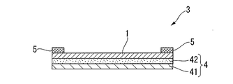
- FIG. 2 is a cross-sectional view of a protective film forming sheet according to another embodiment of the present invention.
- the protective film forming sheet 3 according to this embodiment includes a dicing sheet 4 in which an adhesive layer 42 is laminated on one surface of a base material 41, and an adhesive layer 42 of the dicing sheet 4.
- the protective film forming film 1 laminated on the side and the jig pressure-sensitive adhesive layer 5 laminated on the peripheral edge of the protective film forming film 1 opposite to the dicing sheet 4 are configured.
- the jig pressure-sensitive adhesive layer 5 is a layer for bonding the protective film forming sheet 3 to a jig such as a ring frame.
- the protective film forming sheet 3 holds and holds the workpiece when the workpiece is processed, and applies a protective film to the workpiece or a workpiece obtained by processing the workpiece. Used to form.
- This protective film is composed of a protective film-forming film 1, preferably a cured protective film-forming film 1.
- the protective film forming sheet 3 according to the present embodiment is used to hold a workpiece when performing division processing or the like on the workpiece, and a workpiece obtained by the division processing includes a protective film.
- the dicing sheet 4 of the protective film forming sheet 3 includes a base material 41 and an adhesive layer 42 laminated on one surface of the base material 41.
- the base material 41 of the dicing sheet 4 is not particularly limited as long as it is suitable for workpiece processing, for example, dicing and expanding of a semiconductor wafer, and is usually a resin-based material. It is comprised from the film (henceforth "resin film”) which uses as a main material.
- resin films include polyethylene films such as low density polyethylene (LDPE) films, linear low density polyethylene (LLDPE) films, and high density polyethylene (HDPE) films, polypropylene films, polybutene films, polybutadiene films, and polymethylpentene films.
- LDPE low density polyethylene
- LLDPE linear low density polyethylene
- HDPE high density polyethylene
- Polyolefin films such as ethylene-norbornene copolymer film and norbornene resin film; ethylene-vinyl acetate copolymer film, ethylene- (meth) acrylic acid copolymer film, ethylene- (meth) acrylic acid ester copolymer
- Ethylene copolymer films such as films; Polyvinyl chloride films such as polyvinyl chloride films and vinyl chloride copolymer films; Polyethylene terephthalate films, Polybutylene films Polyester film such as terephthalate film; polyurethane film; polyimide film; polystyrene films; polycarbonate films; and fluorine resin film. Further, modified films such as these crosslinked films and ionomer films are also used.
- the substrate 41 may be a film made of one of these, or may be a laminated film in which two or more of these are combined.
- (meth) acrylic acid in the present specification means both acrylic acid and methacrylic acid. The same applies to other similar terms.
- polyolefin films are preferred from the viewpoints of environmental safety, cost, etc.
- polypropylene films having excellent heat resistance are preferred. If it is a polypropylene film, heat resistance can be provided to the base material 41, without impairing the expandability of the dicing sheet 4 and the pick-up property of a chip. Since the base material 41 has such heat resistance, even when the protective film forming film 1 is heat-cured in a state where the protective film forming sheet 3 is attached to a workpiece, the occurrence of slack in the dicing sheet 4 is suppressed. Can do.
- the resin film may be subjected to a surface treatment such as an oxidation method or a concavo-convex method or a primer treatment on one or both sides as desired for the purpose of improving the adhesion with the pressure-sensitive adhesive layer 42 laminated on the surface.
- a surface treatment such as an oxidation method or a concavo-convex method or a primer treatment on one or both sides as desired for the purpose of improving the adhesion with the pressure-sensitive adhesive layer 42 laminated on the surface.
- a surface treatment such as an oxidation method or a concavo-convex method or a primer treatment on one or both sides as desired for the purpose of improving the adhesion with the pressure-sensitive adhesive layer 42 laminated on the surface.
- the oxidation method include corona discharge treatment, plasma discharge treatment, chromium oxidation treatment (wet), flame treatment, hot air treatment, ozone, ultraviolet irradiation treatment, and the like.
- a thermal spraying method include a thermal spraying method.
- the base material 41 may contain various additives such as a colorant, a flame retardant, a plasticizer, an antistatic agent, a lubricant, and a filler in the resin film.
- the thickness of the base material 41 is not particularly limited as long as it can function properly in each process in which the protective film forming sheet 3 is used.
- the range is preferably 20 to 450 ⁇ m, more preferably 25 to 400 ⁇ m, and particularly preferably 50 to 350 ⁇ m.
- the breaking elongation of the base material 41 of the dicing sheet 4 in this embodiment is preferably 100% or more as a value measured at 23 ° C. and a relative humidity of 50%, particularly preferably 200 to 1000%.
- the elongation at break is the elongation relative to the original length of the test piece at the time of breaking the test piece in a tensile test according to JIS K7161: 1994 (ISO 527-1 1993).
- the base material 41 having a breaking elongation of 100% or more is not easily broken during the expanding process, and the chips formed by cutting the workpiece can be easily separated.
- the tensile stress at 25% strain of the base material 41 of the dicing sheet 4 in this embodiment is preferably 5 to 15 N / 10 mm, and the maximum tensile stress is preferably 15 to 50 MPa.
- the tensile stress at 25% strain and the maximum tensile stress are measured by a test based on JIS K7161: 1994.
- the substrate 2 is loosened when a workpiece is bonded to the dicing sheet 4 and then fixed to a frame such as a ring frame. Generation
- production is suppressed and it can prevent that a conveyance error arises.
- the dicing sheet 4 itself is prevented from peeling off from the ring frame during the expanding process.
- the elongation at break, the tensile stress at 25% strain, and the maximum tensile stress are values measured in the longitudinal direction of the original fabric in the base material 41.
- the pressure-sensitive adhesive layer 42 included in the dicing sheet 4 of the protective film-forming sheet 3 according to the present embodiment may be composed of a non-energy ray-curable pressure-sensitive adhesive or energy ray-curable. You may be comprised from an adhesive.
- the non-energy ray curable pressure-sensitive adhesive those having desired adhesive strength and removability are preferable.
- Polyvinyl ether-based pressure-sensitive adhesives can be used.
- an acrylic pressure-sensitive adhesive that has high adhesiveness with the protective film-forming film 1 and can effectively prevent the workpiece or workpiece from falling off in a dicing process or the like is preferable.
- the adhesive strength of the energy ray curable adhesive decreases when irradiated with energy rays, when the workpiece or workpiece and the dicing sheet 4 are desired to be separated, they can be easily separated by irradiating them with energy rays. it can.
- the pressure-sensitive adhesive layer 42 in the protective film forming sheet 3 is preferably cured. Since the material obtained by curing the energy ray-curable pressure-sensitive adhesive usually has a high elastic modulus and high surface smoothness, the protective film-forming film 3 in contact with the cured portion made of the material is cured to protect the film. When the surface is formed, the surface of the protective film that is in contact with the cured portion has high smoothness (gloss) and is excellent in appearance as a protective film for the chip. Further, when laser printing is performed on a protective film having high surface smoothness, the visibility of the printing is improved.
- the energy ray-curable pressure-sensitive adhesive constituting the pressure-sensitive adhesive layer 42 may be mainly composed of a polymer having energy ray-curability, or a polymer having no energy ray-curability and a lot of energy ray-curable properties. It may be based on a mixture of a functional monomer and / or an oligomer.
- the energy ray curable adhesive is mainly composed of a polymer having energy ray curable properties.
- the polymer having energy ray curability is a (meth) acrylic acid ester (co) polymer (A) (hereinafter referred to as “energy ray”) in which a functional group having energy ray curability (energy ray curable group) is introduced into the side chain. It may be referred to as “curable polymer (A)”).
- This energy ray curable polymer (A) includes a (meth) acrylic copolymer (a1) having a functional group-containing monomer unit, and an unsaturated group-containing compound (a2) having a substituent bonded to the functional group. It is preferable that it is obtained by making it react.
- the acrylic copolymer (a1) is composed of a structural unit derived from a functional group-containing monomer and a structural unit derived from a (meth) acrylic acid ester monomer or a derivative thereof.
- the functional group-containing monomer as a constituent unit of the acrylic copolymer (a1) is a monomer having a polymerizable double bond and a functional group such as a hydroxyl group, an amino group, a substituted amino group, or an epoxy group in the molecule. It is preferable that
- the functional group-containing monomer examples include 2-hydroxyethyl (meth) acrylate, 2-hydroxypropyl (meth) acrylate, 3-hydroxypropyl (meth) acrylate, 4-hydroxybutyl (meth) acrylate, and the like. These may be used alone or in combination of two or more.
- Examples of the (meth) acrylic acid ester monomer constituting the acrylic copolymer (a1) include alkyl (meth) acrylates having 1 to 20 carbon atoms in the alkyl group, cycloalkyl (meth) acrylates, and benzyl (meth) acrylates. Is used. Among these, particularly preferred are alkyl (meth) acrylates having an alkyl group having 1 to 18 carbon atoms, such as methyl (meth) acrylate, ethyl (meth) acrylate, propyl (meth) acrylate, and n-butyl (meth) acrylate. 2-ethylhexyl (meth) acrylate or the like is used.
- the acrylic copolymer (a1) usually contains 3 to 100% by mass, preferably 5 to 40% by mass of a structural unit derived from the functional group-containing monomer, and is a (meth) acrylic acid ester monomer or its
- the structural unit derived from the derivative is usually contained in a proportion of 0 to 97% by mass, preferably 60 to 95% by mass.
- the acrylic copolymer (a1) can be obtained by copolymerizing a functional group-containing monomer as described above with a (meth) acrylic acid ester monomer or a derivative thereof in a conventional manner. Dimethylacrylamide, vinyl formate, vinyl acetate, styrene and the like may be copolymerized.
- an energy beam curable polymer (A ) Is obtained.
- the substituent of the unsaturated group-containing compound (a2) can be appropriately selected according to the type of functional group of the functional group-containing monomer unit of the acrylic copolymer (a1).
- the substituent is preferably an isocyanate group or an epoxy group
- the substituent is an amino group, a carboxyl group or an aziridinyl group. preferable.
- the unsaturated group-containing compound (a2) contains 1 to 5, preferably 1 to 2, energy-polymerizable carbon-carbon double bonds per molecule.
- Specific examples of such unsaturated group-containing compound (a2) include, for example, 2-methacryloyloxyethyl isocyanate, meta-isopropenyl- ⁇ , ⁇ -dimethylbenzyl isocyanate, methacryloyl isocyanate, allyl isocyanate, 1,1- ( Bisacryloyloxymethyl) ethyl isocyanate; acryloyl monoisocyanate compound obtained by reaction of diisocyanate compound or polyisocyanate compound with hydroxyethyl (meth) acrylate; diisocyanate compound or polyisocyanate compound, polyol compound, and hydroxyethyl (meth) Acryloyl monoisocyanate compound obtained by reaction with acrylate; glycidyl (meth) acrylate; (meth) acrylic acid, 2-
- the unsaturated group-containing compound (a2) is usually used in a proportion of 10 to 100 equivalents, preferably 20 to 95 equivalents, per 100 equivalents of the functional group-containing monomer of the acrylic copolymer (a1).
- the reaction temperature, pressure, solvent, time, presence of catalyst, catalyst can be selected as appropriate.
- the functional group present in the acrylic copolymer (a1) reacts with the substituent in the unsaturated group-containing compound (a2), so that the unsaturated group is contained in the acrylic copolymer (a1). It introduce
- the weight average molecular weight of the energy ray curable polymer (A) thus obtained is preferably 10,000 or more, particularly preferably 150,000 to 1,500,000, and more preferably 200,000 to 1,000,000. Is preferred.
- the weight average molecular weight (Mw) in this specification is the value of polystyrene conversion measured by the gel permeation chromatography method (GPC method).
- the energy ray-curable pressure-sensitive adhesive is mainly composed of a polymer having energy ray-curability
- the energy ray-curable pressure-sensitive adhesive further contains an energy ray-curable monomer and / or oligomer (B). May be.
- the energy ray-curable monomer and / or oligomer (B) for example, an ester of a polyhydric alcohol and (meth) acrylic acid or the like can be used.
- Examples of the energy ray-curable monomer and / or oligomer (B) include monofunctional acrylic acid esters such as cyclohexyl (meth) acrylate and isobornyl (meth) acrylate, trimethylolpropane tri (meth) acrylate, penta Erythritol tri (meth) acrylate, pentaerythritol tetra (meth) acrylate, dipentaerythritol hexa (meth) acrylate, 1,4-butanediol di (meth) acrylate, 1,6-hexanediol di (meth) acrylate, polyethylene glycol Polyfunctional acrylic esters such as di (meth) acrylate and dimethyloltricyclodecane di (meth) acrylate, polyester oligo (meth) acrylate, polyurethane oligo (meta Acrylate, and the like.
- monofunctional acrylic acid esters such as
- the content of the energy ray curable monomer and / or oligomer (B) in the energy ray curable pressure-sensitive adhesive is 5 to 80% by mass. It is preferable that the content be 20 to 60% by mass.
- photopolymerization initiator (C) examples include benzophenone, acetophenone, benzoin, benzoin methyl ether, benzoin ethyl ether, benzoin isopropyl ether, benzoin isobutyl ether, benzoin benzoic acid, benzoin methyl benzoate, benzoin dimethyl ketal, 2,4-diethylthioxanthone, 1-hydroxycyclohexyl phenyl ketone, benzyldiphenyl sulfide, tetramethylthiuram monosulfide, azobisisobutyronitrile, benzyl, dibenzyl, diacetyl, ⁇ -chloranthraquinone, (2,4 6-trimethylbenzyldiphenyl) phosphine oxide, 2-benzothiazole-N, N-diethyldithiocarbamate, oligo ⁇ 2-hydroxy-2-me Le-1- [4-
- the photopolymerization initiator (C) is energy beam curable copolymer (A) (when energy beam curable monomer and / or oligomer (B) is blended, energy beam curable copolymer (A). And energy ray-curable monomer and / or oligomer (B) in a total amount of 100 parts by weight) used in an amount in the range of 0.1 to 10 parts by weight, in particular 0.5 to 6 parts by weight with respect to 100 parts by weight. It is preferred that
- other components may be appropriately blended in addition to the above components.
- other components include a polymer component or oligomer component (D) that does not have energy beam curability, and a crosslinking agent (E).
- Examples of the polymer component or oligomer component (D) having no energy ray curability include polyacrylates, polyesters, polyurethanes, polycarbonates, polyolefins, etc., and polymers having a weight average molecular weight (Mw) of 3,000 to 2.5 million. Or an oligomer is preferable.
- crosslinking agent (E) a polyfunctional compound having reactivity with the functional group of the energy beam curable copolymer (A) or the like can be used.
- polyfunctional compounds include isocyanate compounds, epoxy compounds, amine compounds, melamine compounds, aziridine compounds, hydrazine compounds, aldehyde compounds, oxazoline compounds, metal alkoxide compounds, metal chelate compounds, metal salts, ammonium salts. And reactive phenol resins.
- the blending amount of these other components is not particularly limited, and is appropriately determined in the range of 0 to 40 parts by mass with respect to 100 parts by mass of the energy beam curable copolymer (A).
- the energy ray curable adhesive is mainly composed of a mixture of a polymer component having no energy ray curable property and an energy ray curable polyfunctional monomer and / or oligomer will be described below.
- the polymer component having no energy beam curability for example, the same components as those of the acrylic copolymer (a1) described above can be used.
- the content of the polymer component having no energy beam curability in the energy beam curable resin composition is preferably 20 to 99.9% by mass, and particularly preferably 30 to 80% by mass.
- the energy ray-curable polyfunctional monomer and / or oligomer the same one as the above-mentioned component (B) is selected.
- the blending ratio of the polymer component having no energy ray curability and the energy ray curable polyfunctional monomer and / or oligomer is 10 to 150 parts by mass of the polyfunctional monomer and / or oligomer with respect to 100 parts by mass of the polymer component.
- the amount is preferably 25 to 100 parts by mass.
- the photopolymerization initiator (C) and the crosslinking agent (E) can be appropriately blended as described above.
- the thickness of the pressure-sensitive adhesive layer 42 is not particularly limited as long as it can function properly in each step in which the protective film forming sheet 3 is used. Specifically, the thickness is preferably 1 to 50 ⁇ m, particularly preferably 2 to 30 ⁇ m, and further preferably 3 to 20 ⁇ m.
- tool what has desired adhesive force and removability is preferable, for example, an acrylic adhesive, a rubber adhesive, a silicone adhesive, a urethane adhesive Polyester-based pressure-sensitive adhesives, polyvinyl ether-based pressure-sensitive adhesives, and the like can be used.
- an acrylic pressure-sensitive adhesive that has high adhesion to a jig such as a ring frame and can effectively prevent the protective film forming sheet 3 from being peeled off from the ring frame or the like in a dicing process or the like is preferable.
- the base material as a core material may intervene in the middle of the thickness direction of the adhesive layer 5 for jigs.
- the thickness of the pressure-sensitive adhesive layer 5 for jigs is preferably 5 to 200 ⁇ m, and particularly preferably 10 to 100 ⁇ m, from the viewpoint of adhesion to a jig such as a ring frame.
- the protective film forming sheet 3 is preferably prepared by separately separating the first laminated body including the protective film forming film 1 and the second laminated body including the dicing sheet 4. After the production, it can be produced by laminating the protective film forming film 1 and the dicing sheet 4 using the first laminated body and the second laminated body, but is not limited thereto. .
- the protective film forming film 1 is formed on the release surface of the first release sheet.
- a coating agent for a protective film-forming film containing a curable adhesive constituting the protective film-forming film 1 and, if desired, further a solvent is prepared, and a roll coater, a knife coater, a roll knife coater, an air knife
- the protective film-forming film 1 is formed by applying to the release surface of the first release sheet with a coating machine such as a coater, die coater, bar coater, gravure coater, curtain coater, and drying.
- the protective film forming film 1 (and the second release sheet) may be formed in a desired shape, for example, a circle. In this case, what is necessary is just to remove suitably the protective film formation film 1 and the excess part of the 2nd peeling sheet which arose by the half cut.
- a coating agent for the pressure-sensitive adhesive layer further containing a pressure-sensitive adhesive constituting the pressure-sensitive adhesive layer 42 and, if desired, a solvent, on the release surface of the third release sheet.
- the pressure-sensitive adhesive layer 42 is formed by applying and drying. Then, the base material 41 is crimped
- the pressure-sensitive adhesive layer 42 when the pressure-sensitive adhesive layer 42 is made of an energy ray-curable pressure-sensitive adhesive, the pressure-sensitive adhesive layer 42 may be irradiated with energy rays at this stage to cure the pressure-sensitive adhesive layer 42 or to protect it.
- the adhesive layer 42 may be cured after being laminated with the film forming film 1.
- the pressure-sensitive adhesive layer 42 When the pressure-sensitive adhesive layer 42 is cured after being laminated with the protective film forming film 1, the pressure-sensitive adhesive layer 42 may be cured before the dicing process, or the pressure-sensitive adhesive layer 42 may be cured after the dicing process.
- energy rays ultraviolet rays, electron beams, etc. are usually used. Irradiation of energy rays varies depending on the kind of energy rays, for example, in the case of ultraviolet rays, preferably 50 ⁇ 1000mJ / cm 2 in quantity, especially 100 ⁇ 500mJ / cm 2 preferably. In the case of an electron beam, about 10 to 1000 krad is preferable.
- the second release sheet in the first laminate is released and the third release sheet in the second laminate is released.
- the protective film forming film 1 exposed in the first laminated body and the adhesive layer 42 of the dicing sheet 4 exposed in the second laminated body are overlapped and pressure bonded.
- the dicing sheet 4 may be half-cut as desired to have a desired shape, for example, a circle having a larger diameter than the protective film-forming film 1. In this case, an excess portion of the dicing sheet 4 generated by the half cut may be removed as appropriate.
- a protective film forming sheet 3 comprising a first release sheet laminated on the side opposite to the dicing sheet 4 is obtained.
- a jig pressure-sensitive adhesive layer 5 is formed on the peripheral edge of the surface of the protective film forming film 1 opposite to the dicing sheet 4.
- the formation method of the adhesive layer 5 for jigs is not limited.
- An example is as follows. First, a coating composition containing a pressure-sensitive adhesive composition for forming the jig pressure-sensitive adhesive layer 5 and, if desired, a solvent is prepared. The coating composition is applied to the release surface of a separately prepared release sheet, and the obtained coating film is dried to form a jig adhesive layer on the release sheet. A release surface of another release sheet is attached to the exposed surface of the adhesive layer for jig on the release sheet, and the release sheet / adhesive layer for release jig / release sheet configuration is provided. A three-layer laminate is obtained.
- the surface of the protective film forming film 1 is affixed to the peripheral edge of the surface opposite to the dicing sheet 4 so that the jig adhesive layer is laminated on the protective film forming film 1.
- the adhesive layer 5 for tools is used.
- the protective film forming sheet 3 having the configuration of FIG. 2 is obtained by peeling the release sheet on the jig pressure-sensitive adhesive layer 5.
- tool may be comprised only from the adhesive layer like said example, and is comprised from the double-sided adhesive tape by which an adhesive layer is laminated
- the protective film forming film 1 of the protective film forming sheet 3 is attached to the semiconductor wafer 6, and the jig adhesive layer 5 is attached to the ring frame 7.
- the protective film forming film 1 may be heated to exhibit adhesiveness if desired.
- the protective film forming film 1 was cured to form a protective film, and the semiconductor wafer 6 having the protective film laminated thereon was laminated on the surface of the dicing sheet 4 functioning as an extensible dicing sheet.
- a stacked structure including the structure (in this specification, such a stacked structure is also referred to as a “first stacked structure”) is obtained.
- the first laminated structure shown in FIG. 4 further includes a jig pressure-sensitive adhesive layer 5 and a ring frame 7.
- the protective film forming film 1 is a thermosetting adhesive
- the protective film forming film 1 may be heated at a predetermined temperature for an appropriate time.
- the first laminated structure is installed in a split processing laser irradiation apparatus, and the position of the surface of the semiconductor wafer 6 covered with the protective film 1 is detected, and then the semiconductor wafer 6 is used by using the processing laser.
- a modified layer is formed inside.
- the protective film forming sheet 3 according to the present embodiment satisfies the above-described conditions regarding the light transmittance, the laser light emitted from the processing laser passes through the laminate of the protective film and the dicing sheet. Even if the semiconductor wafer 6 is irradiated, the modified layer can be easily formed.
- a force (tensile force in the in-plane direction) is applied to the semiconductor wafer 6 on which the protective film is laminated.
- the semiconductor wafer 6 on which the protective film to be attached to the dicing sheet 4 is laminated is divided to obtain a chip on which the protective film is laminated.
- the chip on which the protective film is laminated is picked up from the dicing sheet 4 using a pickup device.
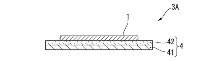
- FIG. 3 is a cross-sectional view of a protective film forming sheet according to still another embodiment of the present invention.
- the protective film forming sheet 3 ⁇ / b> A includes a dicing sheet 4 in which an adhesive layer 42 is laminated on one surface of a base material 41, and an adhesive layer 42 of the dicing sheet 4. And a protective film forming film 1 laminated on the side.
- the protective film forming film 1 in the embodiment is formed to be substantially the same as or slightly larger than the work in the surface direction, and smaller than the dicing sheet 4 in the surface direction.
- the part of the pressure-sensitive adhesive layer 42 where the protective film forming film 1 is not laminated can be attached to a jig such as a ring frame.
- each member of the protective film forming sheet 3A is the same as the material and thickness of each member of the protective film forming sheet 3 described above.
- the pressure-sensitive adhesive layer 42 is made of an energy ray-curable pressure-sensitive adhesive
- the portion in contact with the protective film forming film 1 in the pressure-sensitive adhesive layer 42 cures the energy ray-curable pressure-sensitive adhesive, and the other portions It is preferable not to cure the energy ray curable adhesive.
- a pressure-sensitive adhesive layer for jigs may be provided separately.
- a method for producing a workpiece from a workpiece using the protective film-forming film 1 or the protective film-forming sheets 3 and 3A according to the present embodiment forms a modified layer on the workpiece. It demonstrates collectively for every object of the modified layer formation process which is a process.
- the target of the modified layer forming step is a workpiece (first case)
- the laser beam in the infrared region is irradiated so as to be focused on the focal point set inside the workpiece, such as a semiconductor wafer, and modified inside the workpiece.
- a first modified layer forming step for forming a quality layer is performed.
- the first protective film forming film 1 is laminated on one surface of the workpiece on which the modified layer is formed (in the case of a semiconductor wafer, the surface opposite to the surface on which the circuit is formed, that is, the back surface).
- a protective film formation film lamination process is performed.
- a workpiece is obtained by performing the following dividing step and protective film forming step.
- dividing step a divided object is obtained by applying a force to the workpiece on which the modified layer is formed and dividing the workpiece. Until this division step is started, the protective film forming film 1 laminated on the work or the surface opposite to the face facing the work in the protective film formed from the protective film forming film 1 Thus, a state in which the dicing sheets 4 are laminated is realized.
- a protective film is formed from the protective film forming film 1.
- the order of performing the dividing step and the protective film forming step is not limited. Either may be the first.
- the protective film forming film 1 contains a thermosetting material as described above
- the protective film forming process is a process including heating, for example, holding at 130 ° C. for 2 hours.
- the dicing sheet 4 is required to be a material that can withstand the heating in the protective film forming step.
- one surface of the workpiece (the workpiece becomes a semiconductor chip when the workpiece is a semiconductor wafer) (the surface when the workpiece is a semiconductor wafer). Is a back surface.)
- a processed product having a protective film stacked thereon is obtained (when the workpiece is a semiconductor wafer, a semiconductor chip having a protective film stacked is a processed product).
- the protective film forming film 1 according to the present embodiment is broken as described above. It is only necessary to satisfy the conditions regarding the index, and when the division processing is performed after the protective film forming step, the protective film formed from the protective film forming film 1 according to the present embodiment satisfies the above-described conditions regarding the fracture index. It only has to be. Whether or not the protective film according to the present embodiment satisfies the above-described conditions regarding the light transmittance does not affect the division workability.
- the laminated state of the protective film and the dicing sheet 4 laminated on the work on which the modified layer is formed is not limited. That is, the protective film-forming film 1 may be laminated on the work on which the modified layer is formed, and the dicing sheet 4 may be laminated on the protective film-forming film 1, or the protective film laminated on the work A protective film may be formed from the forming film 1, and the dicing sheet 4 may be laminated
- the protective film forming sheets 3 and 3A may be laminated on the work on which the modified layer is formed. When the protective film forming sheets 3 and 3A are laminated, the protective film forming film 1 laminated on the workpiece is in a state where the dicing sheet 4 is laminated on one surface.
- the work is irradiated with infrared laser light through the protective film forming film 1 so as to be focused on the focal point set inside the work on which the protective film forming film 1 is laminated.
- a second modified layer forming step for forming the modified layer is performed. Since the laser beam is irradiated onto the workpiece through the protective film forming film 1, in the case of the second case, it is preferable that the protective film forming film 1 satisfies the above-described conditions regarding the light transmittance.
- a workpiece is obtained by performing the above-described dividing step and protective film forming step.
- the order of performing the dividing step and the protective film forming step is arbitrary.
- the division processing is performed before the protective film forming step, it is only necessary that the protective film forming film 1 satisfies the above-described conditions regarding the fracture index.
- the division processing is performed after the protective film forming step, it is only necessary that the protective film satisfies the above-described conditions regarding the fracture index.
- the laminated state of the protective film or the like and the dicing sheet 4 laminated on the workpiece is not limited.
- the laser light passes through the protective film forming film 1. Therefore, the protective film forming sheets 3 and 3A are not laminated on the workpiece. That is, after the second modified layer forming step, a step of laminating the dicing sheet is performed on the protective film or the like that is laminated on the workpiece on which the modified layer is formed.
- the protective film forming film 1 and the dicing sheet 4 (third case)
- the object of the modified layer forming step is a laminated structure of the workpiece
- the protective film forming film 1 and the dicing sheet 4 first, the protective film forming film 1 laminated on one surface of the workpiece and the workpiece.
- a laminated structure including a dicing sheet 4 laminated on the surface opposite to the side facing the workpiece of the protective film forming film 1 is prepared.
- this laminated structure can be obtained by laminating the protective film forming sheets 3 and 3A on the workpiece.
- a laser beam in the infrared region is irradiated from the dicing sheet 4 side to form a modified layer inside the work so that the work of this laminated structure is focused on a focal point set inside the work.
- a modified layer forming step is performed. Since the laser beam is irradiated onto the workpiece through the dicing sheet 4 and the protective film forming film 1, in the case of the third case, the protective film forming film 1 preferably satisfies the above-described conditions regarding the light transmittance. . In the case of the third case, when the protective film forming sheets 3 and 3A are used, it is preferable that the protective film forming sheets 3 and 3A also satisfy the conditions regarding the light transmittance.
- a workpiece is obtained by performing the above-described dividing step and protective film forming step.
- the order of performing the dividing step and the protective film forming step is arbitrary.
- work is not limited.
- the laminated body of the protective film formation film 1 and the dicing sheet 4 should just be appropriately laminated
- the protective film forming film 1 may be first laminated on the workpiece, and then the dicing sheet 4 may be laminated, or the protective film forming sheets 3 and 3A may be laminated on the workpiece. .
- a second protective film forming film laminating step is performed in which the protective film forming film 1 is laminated on one surface of the workpiece.
- the protective film formation process which forms a protective film from the protective film formation film 1 is performed.
- an infrared laser beam is irradiated to the work through the protective film so as to be focused on a focal point set inside the work on which the protective film is laminated, thereby forming a modified layer inside the work.
- a fourth modified layer forming step is performed.
- the protective film satisfies the above-described conditions regarding the light transmittance.
- the protective film formation film 1 should just satisfy
- a dividing step is performed in which a divided product is obtained by applying a force to the workpiece on which the modified layer is formed to divide the workpiece.
- protection is performed on one surface of the divided product.
- a processed product in which films are laminated is obtained. Therefore, in the case of the fourth case, it is only necessary that the protective film satisfies the above-described conditions regarding the fracture index.
- the target of the modified layer forming step is a laminated structure of the workpiece, the protective film, and the dicing sheet 4 (fifth case)
- the target of the modified layer forming step is a laminated structure of the workpiece, the protective film, and the dicing sheet 4, a step of preparing this laminated structure is first performed.
- Methods for preparing this laminated structure include sequential lamination and batch lamination.
- the second protective film forming film laminating step of laminating the protective film forming film 1 on one surface of the work, the protective film forming step of forming the protective film from the protective film forming film 1, and the work piece are laminated.
- a second dicing sheet laminating step for laminating the dicing sheet 4 on the protective film is performed.
- the 3rd protective film formation film lamination process which laminates
- the protective film forming sheets 3 and 3A may be laminated on the workpiece. Then, the protective film formation process which forms a protective film from the protective film formation film 1 is performed.
- the laser beam in the infrared region is irradiated to the work through the protective film and the dicing sheet 4 so as to be focused on the focal point set inside the work of the laminated structure thus obtained, and modified inside the work.
- the fifth modified layer forming step for forming a layer is performed. Since the laser beam is irradiated onto the workpiece through the dicing sheet 4 and the protective film, in the case of the fifth case, it is preferable that the protective film forming film 1 satisfies the above-described conditions regarding the light transmittance. In the case of the fifth case, when the protective film forming sheets 3 and 3A are used, it is preferable that the protective film forming sheets 3 and 3A also satisfy the above-described conditions regarding the light transmittance.
- a dividing step is performed in which a divided product is obtained by applying a force to the workpiece on which the modified layer is formed and dividing the workpiece, and as a result of the dividing step, on one surface of the divided product.
- a workpiece obtained by laminating a protective film is obtained. Therefore, in the case of the fifth case, it is only necessary that the protective film satisfies the above-described conditions regarding the fracture index.
- a release sheet may be laminated on the side opposite to the dicing sheet 4 in the protective film forming film 1 of the protective film forming sheets 3 and 3A.
- Examples 1 to 9 and Comparative Examples 1 and 2 Each of the following components was mixed at a blending ratio (solid content conversion part by mass) shown in Table 1, and diluted with methyl ethyl ketone so that the solid content concentration was 61% by mass to prepare a coating agent for a protective film forming film. .
- A-1) Polymer component: acrylic polymer (weight) obtained by copolymerizing 10 parts by mass of n-butyl acrylate, 70 parts by mass of methyl acrylate, 5 parts by mass of glycidyl methacrylate, and 15 parts by mass of 2-hydroxyethyl acrylate (Average molecular weight: 800,000, glass transition temperature: -1 ° C)
- A-2) Polymer component: acrylic polymer obtained by copolymerizing 55 parts by mass of n-butyl acrylate, 10 parts by mass of methyl acrylate, 20 parts by mass of glycidyl methacrylate, and 15 parts by mass of 2-hydroxyethyl acrylate (weight) (Average molecular weight: 800,000, glass transition temperature: -28 ° C)
- A-3) Polymer component: acrylic polymer obtained by copolymerizing 85 parts by mass of methyl acrylate and 15 parts by mass of 2-hydroxyethyl acrylate (weight average molecular weight
- the first release sheet R (SP-PET 382150, thickness 38 ⁇ m) made by forming a silicone release agent layer on one side of a polyethylene terephthalate (PET) film, and the silicone release on one side of the PET film
- a second release sheet R ′ (manufactured by Lintec Corporation, SP-PET 381031, thickness 38 ⁇ m) formed with an agent layer was prepared.
- the thickness of the final protective film forming film P 0 obtained was coated to a 25 [mu] m, in an oven The film was dried at 120 ° C. for 2 minutes to form a protective film-forming film P 0 .
- the release surface of the second release sheet R ′ is bonded to the surface of the obtained protective film forming film P 0 , and the first release sheet R (release sheet 21 in FIG. 1) and the protective film forming film are bonded.
- a protective film forming sheet RP 0 R ′ composed of P 0 (protective film forming film 1 in FIG. 1) (thickness: 25 ⁇ m) and the second release sheet R ′ was obtained.
- a protective film-forming sheet RP 0 R ′ is separately prepared by the above method, the second release sheet R ′ is peeled off, and the surface of the protective film-forming film P 0 exposed is diced sheet D (manufactured by Lintec Corporation). “Adwill D-821HS”) was prepared on the surface of the pressure-sensitive adhesive layer, and a laminate [P 0 D] composed of the protective film-forming film P 0 and the dicing sheet D was applied to the surface on the protective film-forming film P 0 side. Obtained with the first release sheet R attached.
- the protective film-forming film P 0 was cut to a width 5 mm ⁇ length 5 mm, it was a test piece consisting of the protective film forming film P 0.
- Test piece formed from the protective film P 1 is a test piece thickness of the can and a protective film forming film P 0 of 50 ⁇ m produced separately, which was prepared by heating under conditions of 130 ° C. 2 hours.
- the protective film forming film P 0 cut into the same shape as the silicon wafer S is pasted on a table heated to 70 ° C. using a pasting apparatus (“RAD-3600 F / 12” manufactured by Lintec), and laser inside to obtain a laminated body SP 0 between the silicon wafer S which modified layer is formed as the protective film forming film P 0 by irradiation.
- a pasting apparatus (“RAD-3600 F / 12” manufactured by Lintec)
- a dicing sheet D (“Adwill D-821HS” manufactured by Lintec) is pasted on the protective film forming film P 0 side of the laminate SP 0 using a bonding device (“RAD-2700 F / 12” manufactured by Lintec).
- RAD-2700 F / 12 manufactured by Lintec
- the division property of the protective film forming film P 0 was evaluated according to the following criteria. First division rate 100%: Excellent division property (“A” in Table 1)
- First split ratio less than 80%: not having allowable split ability (“D” in Table 1) The evaluation results are shown in Table 2.
- the protective film forming film P 0 is cut into the same shape as that of the silicon wafer S, and is applied to the silicon wafer S in which the modified layer is formed inside using a sticking device (“RAD-3600 F / 12” manufactured by Lintec Corporation).
- a sticking device (“RAD-3600 F / 12” manufactured by Lintec Corporation).
- the protective film forming film P 0 after the cutting process is pasted on a table heated to 70 ° C., and the laminate SP of the silicon wafer S having the modified layer formed therein and the protective film forming film P 0. 0 was obtained.
- the laminate SP 0 under an air atmosphere and heated for 2 hours at 130 ° C., to form the protective film P 1 from the protective film forming film P 0 the stack SP 0 comprising, reforming layer is formed inside the laminate SP 1 made of a silicon wafer S and the protective film P 1 Metropolitan was obtain.
- a dicing sheet D (“Adwill D-821HS” manufactured by Lintec) is pasted on the protective film P 1 side of the laminate SP 1 using a bonding device (“RAD-2700 F / 12” manufactured by Lintec).
- the temperature of the stacked body SP 1 D including the silicon wafer S in which the modified layer is formed is maintained at 0 ° C., and a pulling rate is 100 mm / second, Expanding was performed with an expanding amount of 10 mm. As a result, at least a part of the silicon wafer S was divided along the division line, and a plurality of chips were obtained.
- the second division ratio (unit:%) is the percentage of was used to evaluate the division of the protective film P 1 on the following criteria. Second split ratio 100%: Excellent splitting ability (“A” in Table 1) Second division ratio of 80% or more and less than 100%: has an allowable division property (“C” in Table 1) Second split ratio less than 80%: not having allowable splitting ability (“D” in Table 1) The evaluation results are shown in Table 2.
- the second release sheet R ′ is peeled from the protective film forming sheet RP 0 R ′ obtained in the examples and comparative examples, and heated in an atmosphere at 130 ° C. for 2 hours in an oven to form a protective film forming film P 0 was thermally cured to obtain a protective film P 1 . Thereafter, by peeling the first release sheet R, it was prepared protective film P 1.
- the surface of the protective film-forming film P 0 of the laminate obtained by peeling the second release sheet R ′ from the protective film-forming sheet RP 0 R ′ obtained in Examples and Comparative Examples, and a dicing sheet D ( A laminate [P 0 D] was prepared by bonding the surface of the pressure-sensitive adhesive layer of “Adwill D-821HS” manufactured by Lintec Corporation.
- the second release sheet R ′ is peeled from the protective film forming sheet RP 0 R ′ obtained in the examples and comparative examples, and heated in an atmosphere at 130 ° C. for 2 hours in an oven to form a protective film forming film P 0 was thermally cured to obtain a protective film P 1 .
- a protective film forming film P 0 was thermally cured to obtain a protective film P 1 .
- the protective film-forming film P 0 , the protective film P 1 , and the laminate [P 0 D] prepared as described above and light transmittance of the laminate P 1 D were measured, the light transmittance of the wavelength 1064 nm (unit:%) were extracted.
- the attached large sample chamber MPC-3100 was used, and measurement was performed using a built-in integrating sphere. The results are shown in Table 2.
- Test Example 5 ⁇ Evaluation of wafer division workability> (Test Example 5-1)
- the object of laser irradiation is the laminate SP 0
- a protective film forming film P 0 cut into the same shape as the silicon wafer S is formed on the silicon wafer S having a thickness of 100 ⁇ m and an outer diameter of 8 inches.
- RAD-3600 F / 12 manufactured by Lintec
- pasting was performed on a table heated to 70 ° C. to obtain a laminate SP 0 of the silicon wafer S and the protective film forming film P 0 . .
- a laser that focuses light inside the silicon wafer is 9 mm ⁇ 9 mm. Irradiation was performed while scanning along a planned cutting line set so that the chip body was formed, and a modified layer was formed inside the silicon wafer S.
- a sticking device (“RAD-2700 F / 12” manufactured by Lintec Co., Ltd.) was used on the protective film forming film P 0 side of the laminate SP 0 including the silicon wafer S having the modified layer formed therein, thus obtained. Then, a dicing sheet D (“Adwill D-821HS” manufactured by Lintec Co., Ltd.) is pasted, and a laminate SP 0 of the silicon wafer S, the protective film forming film P 0 and the dicing sheet D on which a modified layer is formed. D was obtained with the ring frame fixed.
- the resulting laminate SP 0 D was maintained at a temperature of 0 ° C., and expanded at a pulling rate of 100 mm / sec and an expanding amount of 10 mm. As a result, at least a part of the silicon wafer S was divided along the division line, and a plurality of chips were obtained.
- the presence or absence of cleaving of the protective film or the like (the protective film forming film P 0 or the protective film P 1 ) is not evaluated, and the silicon wafer S is aligned along all the planned cutting lines of the silicon wafer S.
- the third division ratio (unit:%), which is the ratio of the number of chips actually obtained with respect to the number of chips obtained when cut, the division property was evaluated according to the following criteria.
- the evaluation results are shown in the column of “Laminated body SP 0 ” in Table 2.
- the obtained laminate SP 0 is heated at 130 ° C. for 2 hours in the air atmosphere to form the protective film P 1 from the protective film forming film P 0 , and the silicon wafer S and the protective film P 1 are laminated.
- the body SP 1 was obtained.
- a laser that focuses light inside the silicon wafer S is a 9 mm ⁇ 9 mm chip body Irradiation was performed while scanning along a planned cutting line set so that a modified layer was formed inside the silicon wafer S.
- a dicing sheet D (“Adwill D-821HS” manufactured by Lintec Co., Ltd.) is pasted, and a laminated body SP 1 D of the silicon wafer S, the protective film P 1 and the dicing sheet D having a modified layer formed therein is a ring frame. Obtained in a fixed state.
- the obtained laminate SP 1 D was expanded at a pulling rate of 100 mm / second and an expanding amount of 10 mm while maintaining the temperature of the laminate SP 1 D at 0 ° C. As a result, at least a part of the silicon wafer S was divided along the division line, and a plurality of chips were obtained.
- a protective film forming film P 0 obtained by cutting a silicon wafer S having a thickness of 100 ⁇ m and an outer diameter of 8 inches into the same shape as the silicon wafer S Is pasted on a table heated to 70 ° C. using a pasting device (“RAD-3600 F / 12” manufactured by Lintec Corporation) to obtain a laminate SP 0 of the silicon wafer S and the protective film forming film P 0. It was.
- a dicing sheet D (“Adwill D-821HS” manufactured by Lintec) is pasted on the protective film forming film P 0 side of the laminate SP 0 using a bonding device (“RAD-2700 F / 12” manufactured by Lintec).
- RAD-2700 F / 12 manufactured by Lintec
- a laser that focuses light inside the silicon wafer S is 9 mm ⁇ 9 mm. Irradiation was performed while scanning along a planned cutting line set to form a chip body, and a modified layer was formed inside the silicon wafer S included in the stacked body SP 0 D.
- the temperature of the obtained laminate S [P 0 D] was maintained at 0 ° C., and the expanding was performed at a pulling-off speed of 100 mm / second and an expanding amount of 10 mm. .
- the expanding apparatus (“DDS2300” manufactured by DISCO)
- the temperature of the obtained laminate S [P 0 D] was maintained at 0 ° C.
- the expanding was performed at a pulling-off speed of 100 mm / second and an expanding amount of 10 mm. .
- the silicon wafer S was divided along the division line, and a plurality of chips were obtained.
- the obtained laminate SP 0 is heated at 130 ° C. for 2 hours in an air atmosphere to form a protective film P 1 from the protective film-forming film P 0, and a laminate of the silicon wafer S and the protective film P 1. SP 1 was obtained.
- a dicing sheet D (“Adwill D-821HS” manufactured by Lintec) is pasted on the protective film P 1 side of the laminate SP 1 using a bonding device (“RAD-2700 F / 12” manufactured by Lintec).
- a laminate SP 1 D of the silicon wafer S, the protective film P 1 and the dicing sheet D was obtained in a state of being fixed to the ring frame.
- the temperature of the stacked body SP 1 D including the silicon wafer S in which the modified layer is formed is maintained at 0 ° C., and a pulling rate is 100 mm / second, Expanding was performed with an expanding amount of 10 mm. As a result, at least a part of the silicon wafer S was divided along the division line, and a plurality of chips were obtained.
- the protective film-forming film laminated on the work to be divided or the protective film-forming film of the example having a break index of the protective film of 1 MPa ⁇ % or more and 250 MPa ⁇ % or less is divided into processability. It was excellent.
- the protective film-forming film and the protective film-forming sheet according to the present invention are suitably used for manufacturing a workpiece such as a chip on which a protective film is laminated from a workpiece such as a semiconductor wafer.
Landscapes
- Chemical & Material Sciences (AREA)
- Organic Chemistry (AREA)
- Engineering & Computer Science (AREA)
- Chemical Kinetics & Catalysis (AREA)
- Polymers & Plastics (AREA)
- Medicinal Chemistry (AREA)
- Health & Medical Sciences (AREA)
- Optics & Photonics (AREA)
- Physics & Mathematics (AREA)
- Wood Science & Technology (AREA)
- Materials Engineering (AREA)
- Life Sciences & Earth Sciences (AREA)
- Mechanical Engineering (AREA)
- Plasma & Fusion (AREA)
- Oil, Petroleum & Natural Gas (AREA)
- General Chemical & Material Sciences (AREA)
- Dicing (AREA)
- Adhesives Or Adhesive Processes (AREA)
- Laser Beam Processing (AREA)
- Adhesive Tapes (AREA)
- Manufacture Of Macromolecular Shaped Articles (AREA)
- Compositions Of Macromolecular Compounds (AREA)
- Electromagnetism (AREA)
- Measurement Of Force In General (AREA)
- Manufacturing Of Magnetic Record Carriers (AREA)
Abstract
Description
(1)保護膜形成フィルムであって、前記保護膜形成フィルムおよび前記保護膜形成フィルムから形成された保護膜の少なくとも一方は、測定温度0℃で測定された破断応力(MPa)と、測定温度0℃で測定された破断ひずみ(単位:%)との積が、1MPa・%以上250MPa・%以下であることを特徴とする保護膜形成フィルム。
1.保護膜形成フィルム
本実施形態に係る保護膜形成フィルムは、ワークまたは当該ワークを加工して得られる加工物に保護膜を形成するためのものである。この保護膜は、保護膜形成フィルム、好ましくは硬化した保護膜形成フィルムから構成される。ワークとしては半導体ウエハが例示され、当該ワークを加工して得られる加工物としては半導体チップが例示されるが、本発明はこれらに限定されるものではない。なお、ワークが半導体ウエハの場合、保護膜は、半導体ウエハの裏面側(バンプ等の電極が形成されていない側)に形成される。
(1-1)破断インデックス
本実施形態に係る保護膜形成フィルムまたは保護膜形成フィルムから形成された保護膜(本明細書において、保護膜形成フィルムおよび保護膜を総称して「保護膜等」ともいう。)は、測定温度0℃で測定された破断応力(MPa)と測定温度0℃で測定された破断ひずみ(単位:%)との積(本明細書において、この積を「破断インデックス」ともいう。)が、1MPa・%以上250MPa・%以下である。
本実施形態に係る保護膜形成フィルムは、波長1064nmの光線透過率が30%以上であることが好ましい。本明細書における光線透過率は、積分球を使用して測定した値とし、測定器具としては分光光度計を使用する。
保護膜形成フィルムは、未硬化の硬化性接着剤からなることが好ましい。この場合には、保護膜形成フィルムにワークを重ね合わせた後、保護膜形成フィルムを硬化させることにより、保護膜をワークに強固に接着することができ、耐久性を有する保護膜をチップなどの分割物に積層することができる。
図1は本発明の一実施形態に係る保護膜形成用シートの断面図である。図1に示すように、本実施形態に係る保護膜形成用シート2は、保護膜形成フィルム1と、保護膜形成フィルム1の一方の面(図1では下側の面)に積層された剥離シート21とを備えて構成される。ただし、剥離シート21は、保護膜形成用シート2の使用時に剥離されるものである。
図2は本発明の他の一実施形態に係る保護膜形成用シートの断面図である。図2に示すように、本実施形態に係る保護膜形成用シート3は、基材41の一方の面に粘着剤層42が積層されてなるダイシングシート4と、ダイシングシート4の粘着剤層42側に積層された保護膜形成フィルム1と、保護膜形成フィルム1におけるダイシングシート4とは反対側の周縁部に積層された治具用粘着剤層5とを備えて構成される。治具用粘着剤層5は、保護膜形成用シート3をリングフレーム等の治具に接着するための層である。
本実施形態に係る保護膜形成用シート3のダイシングシート4は、基材41と、基材41の一方の面に積層された粘着剤層42とを備えて構成される。
ダイシングシート4の基材41は、ワークの加工、例えば半導体ウエハのダイシングおよびエキスパンディングに適するものであれば、その構成材料は特に限定されず、通常は樹脂系の材料を主材とするフィルム(以下「樹脂フィルム」という。)から構成される。
本実施形態に係る保護膜形成用シート3のダイシングシート4が備える粘着剤層42は、非エネルギー線硬化性粘着剤から構成されてもよいし、エネルギー線硬化性粘着剤から構成されてもよい。非エネルギー線硬化性粘着剤としては、所望の粘着力および再剥離性を有するものが好ましく、例えば、アクリル系粘着剤、ゴム系粘着剤、シリコーン系粘着剤、ウレタン系粘着剤、ポリエステル系粘着剤、ポリビニルエーテル系粘着剤等を使用することができる。これらの中でも、保護膜形成フィルム1との密着性が高く、ダイシング工程等にてワークまたは加工物の脱落を効果的に抑制することのできるアクリル系粘着剤が好ましい。
保護膜形成用シート3は、好ましくは、保護膜形成フィルム1を含む第1の積層体と、ダイシングシート4を含む第2の積層体とを別々に作製した後、第1の積層体および第2の積層体を使用して、保護膜形成フィルム1とダイシングシート4とを積層することにより製造することができるが、これに限定されるものではない。
本実施形態に係る保護膜形成用シート3の使用方法の一例として、ワークとしての半導体ウエハから、加工物としての保護膜が積層されたチップを製造する方法を以下に説明する。
図3は本発明のさらに他の一実施形態に係る保護膜形成用シートの断面図である。図3に示すように、本実施形態に係る保護膜形成用シート3Aは、基材41の一方の面に粘着剤層42が積層されてなるダイシングシート4と、ダイシングシート4の粘着剤層42側に積層された保護膜形成フィルム1とを備えて構成される。実施形態における保護膜形成フィルム1は、面方向にてワークとほぼ同じか、ワークよりも少し大きく形成されており、かつダイシングシート4よりも面方向に小さく形成されている。保護膜形成フィルム1が積層されていない部分の粘着剤層42は、リングフレーム等の治具に貼付することが可能となっている。
以下、本実施形態に係る保護膜形成フィルム1または保護膜形成用シート3,3Aを用いて、ワークから加工物を製造する方法について、ワークに対して改質層を形成する工程である改質層形成工程の対象ごとにまとめて説明する。
改質層形成工程の対象がワーク単体である場合には、まず、半導体ウエハなどのワークの内部に設定された焦点に集束されるように赤外域のレーザー光を照射して、ワーク内部に改質層を形成する第1改質層形成工程が行われる。次に、改質層が形成されたワークの一の面(半導体ウエハの場合には、回路が形成された面の反対側の面、すなわち裏面)に、保護膜形成フィルム1を積層する第1保護膜形成フィルム積層工程が行われる。
改質層形成工程の対象がワークと保護膜形成フィルム1との積層構造体である場合には、まず、保護膜形成フィルム1をワークの一の面に積層する第2保護膜形成フィルム積層工程が行われる。
改質層形成工程の対象がワークと保護膜形成フィルム1とダイシングシート4との積層構造体である場合には、まず、ワークと、ワークの一の面に積層された、保護膜形成フィルム1と、保護膜形成フィルム1のワークに対向する側と反対側の面に積層されたダイシングシート4とを備えた積層構造体を用意する。一例として、保護膜形成用シート3,3Aをワークに積層することによりこの積層構造体を得ることができる。
改質層形成工程の対象がワークと保護膜との積層構造体である場合には、保護膜形成フィルム1をワークの一の面に積層する第2保護膜形成フィルム積層工程が行われる。次に、保護膜形成フィルム1から保護膜を形成する保護膜形成工程が行われる。続いて、保護膜が積層されたワークの内部に設定された焦点に集束されるように、赤外域のレーザー光を、保護膜越しにワークに照射して、ワーク内部に改質層を形成する第4改質層形成工程が行われる。したがって、第4ケースの場合には、保護膜が前述の光線透過率に関する条件を満たすことが好ましい。そのためには、保護膜形成フィルム1が前述の光線透過率に関する条件を満たせばよい。
改質層形成工程の対象がワークと保護膜とダイシングシート4との積層構造体である場合には、まず、この積層構造体を用意する工程が行われる。この積層構造体を用意する方法には、逐次積層と一括積層とがある。
次の各成分を表1に示される配合比(固形分換算質量部)で混合し、固形分濃度が61質量%となるようにメチルエチルケトンで希釈して、保護膜形成フィルム用塗布剤を調製した。
(A-1)重合体成分:n-ブチルアクリレート10質量部、メチルアクリレート70質量部、グリシジルメタクリレート5質量部、および2-ヒドロキシエチルアクリレート15質量部を共重合してなるアクリル系重合体(重量平均分子量:80万、ガラス転移温度:-1℃)
(A-2)重合体成分:n-ブチルアクリレート55質量部、メチルアクリレート10質量部、グリシジルメタクリレート20質量部、および2-ヒドロキシエチルアクリレート15質量部を共重合してなるアクリル系重合体(重量平均分子量:80万、ガラス転移温度:-28℃)
(A-3)重合体成分:メチルアクリレート85質量部および2-ヒドロキシエチルアクリレート15質量部を共重合してなるアクリル系重合体(重量平均分子量:80万、ガラス転移温度:6℃)
(B-1)ビスフェノールA型エポキシ樹脂(三菱化学社製「jER828」、エポキシ当量184~194g/eq)
(B-2)ジシクロペンタジエン型エポキシ樹脂(大日本インキ化学工業社製「エピクロンHP-7200HH」、エポキシ当量255~260g/eq)
(B-3)ビスフェノールA型エポキシ樹脂(三菱化学社製「jER1055」、エポキシ当量800~900g/eq)
(B-4)固体エポキシ樹脂:フェノールノボラック型エポキシ樹脂(日本化薬社製「EPPN502H」、エポキシ当量167g/eq)
(B-5)アクリロイル基付加クレゾールノボラック型エポキシ樹脂(日本化薬社製「CNA-147」、エポキシ当量518g/eq、数平均分子量2100、不飽和基含有量:エポキシ基と等量)
(C-1)熱活性潜在性エポキシ樹脂硬化剤:ジシアンジアミド(ADEKA社製「アデカハードナーEH-3636AS」、活性水素量21g/eq)
(C-2)硬化促進剤:2-フェニル-4,5-ジヒドロキシメチルイミダゾール(四国化成工業社製「キュアゾール2PHZ」)
(C-3)熱硬化剤:アラルキル型フェノール樹脂(三井化学社製「ミレックスXLC-4L」)
(D)シリカフィラー(アドマテックス社製「SC2050MA」、平均粒子径0.5μm)
(E)着色剤:カーボンブラック(三菱化学社製「#MA650」、平均粒径28nm)
(F)イソシアナート化合物(東洋インキ製造社製「BHS-8515」)
(G)シランカップリング剤(信越化学工業社製「KBM403」)
(H)熱可塑性樹脂(東洋紡績社製「バイロン220」)

動的機械分析装置(ティー・エイ・インスツルメント社製「DMA Q800」)を用いて、保護膜形成フィルムP0および保護膜形成フィルムP0から形成された保護膜P1の引張り試験を行った。実施例および比較例で得られた保護膜形成用シートRP0R’の2枚について、第2の剥離シートR’を剥離し、表出させた保護膜形成フィルムP0の面が対向するように、これらの保護膜形成用シートRP0を貼付し、それぞれの第1の剥離シートRを剥離させることにより、厚さが50μmの保護膜形成フィルムP0を得て、この保護膜形成フィルムP0を幅5mm×長さ5mmに裁断して、保護膜形成フィルムP0からなる試験片とした。保護膜P1からなる試験片は、上記の厚さが50μmの保護膜形成フィルムP0からなる試験片を別途作製し、これを130℃2時間の条件で加熱することにより用意した。
ワークとしての厚さ100μm、外径8インチのシリコンウエハSに、レーザー照射装置(DISCO社製「DFL7360」、レーザー波長:1064nm)を用いて、シリコンウエハS内部で集光するレーザーを、9mm×9mmのチップ体が形成されるように設定された切断予定ラインに沿って走査させながら照射しシリコンウエハS内部に改質層を形成した。
第1分割率100%:分割性優良(表1中「A」)
第1分割率80%以上100%未満:許容される分割性を有する(表1中「C」)
第1分割率80%未満:許容される分割性を有しない(表1中「D」)
評価結果を表2に示す。
厚さ100μm、外径8インチのシリコンウエハSに、レーザー照射装置(DISCO社製「DFL7360」、レーザー波長:1064nm)を用いて、シリコンウエハS内部で集光するレーザーを、9mm×9mmのチップ体が形成されるように設定された切断予定ラインに沿って走査させながら照射しシリコンウエハS内部に改質層を形成した。
第2分割率100%:分割性優良(表1中「A」)
第2分割率80%以上100%未満:許容される分割性を有する(表1中「C」)
第2分割率80%未満:許容される分割性を有しない(表1中「D」)
評価結果を表2に示す。
実施例および比較例で得られた保護膜形成用シートRP0R’から第1の剥離シートRおよび第2の剥離シートR’を剥離して、保護膜形成フィルムP0を用意した。
(試験例5-1)レーザー照射対象が積層体SP0である場合
厚さ100μm、外径8インチのシリコンウエハSに、シリコンウエハSと同形状に切断加工された保護膜形成フィルムP0を、貼付装置(リンテック社製「RAD-3600 F/12」)を用いて70℃に加熱したテーブル上で貼付して、シリコンウエハSと保護膜形成フィルムP0との積層体SP0を得た。
第3分割率100%:分割性優良(表1中「A」)
第3分割率95%以上100%未満:分割性良好(表1中「B」)
第3分割率80%以上95%未満:許容される分割性を有する(表1中「C」)
第3分割率80%未満:許容される分割性を有しない(表1中「D」)
評価結果を表2の「積層体SP0」の列に示す。
厚さ100μm、外径8インチのシリコンウエハSに、シリコンウエハSと同形状に切断加工された保護膜形成フィルムP0を、貼付装置(リンテック社製「RAD-3600 F/12」)を用いて70℃に加熱したテーブル上で貼付して、シリコンウエハSと保護膜形成フィルムP0との積層体SP0を得た。
厚さ100μm、外径8インチのシリコンウエハSに、シリコンウエハSと同形状に切断加工された保護膜形成フィルムP0を、貼付装置(リンテック社製「RAD-3600 F/12」)を用いて70℃に加熱したテーブル上で貼付して、シリコンウエハSと保護膜形成フィルムP0との積層体SP0を得た。
厚さ100μm、外径8インチのシリコンウエハSに、貼付装置(リンテック社製「RAD-2700 F/12」)を用いて、ダイシングシートとしての機能を有する保護膜形成用シート[P0D]を70℃に加熱したテーブル上で貼付して、シリコンウエハSと保護膜形成用シート[P0D]との積層体S[P0D]をリングフレームに固定された状態で得た。
厚さ100μm、外径8インチのシリコンウエハSに、シリコンウエハSと同形状に切断加工された保護膜形成フィルムP0を、貼付装置(リンテック社製「RAD-3600 F/12」)を用いて70℃に加熱したテーブル上で貼付して、シリコンウエハSと保護膜形成フィルムP0との積層体SP0を得た。
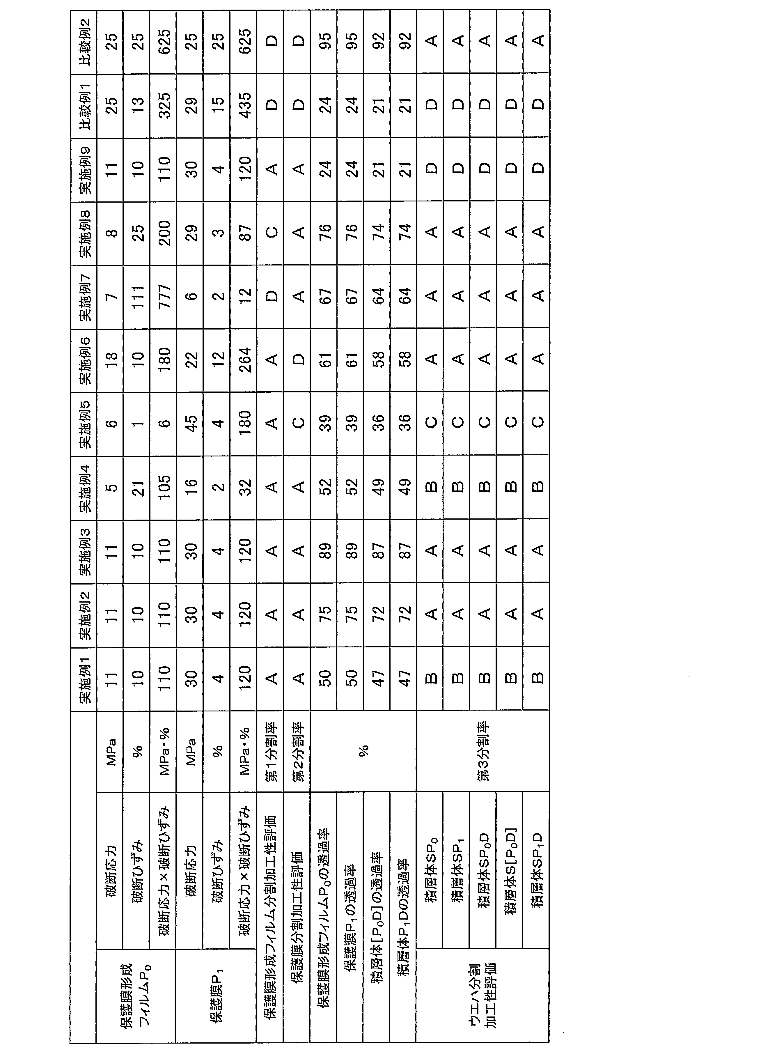
2…保護膜形成用シート
21…剥離シート
3,3A…保護膜形成用シート
4…ダイシングシート
41…基材
42…粘着剤層
5…治具用粘着剤層
6…半導体ウエハ
7…リングフレーム
Claims (14)
- 保護膜形成フィルムであって、
前記保護膜形成フィルムおよび前記保護膜形成フィルムから形成された保護膜の少なくとも一方は、
測定温度0℃で測定された破断応力(MPa)と、測定温度0℃で測定された破断ひずみ(単位:%)との積が、1MPa・%以上250MPa・%以下であること
を特徴とする保護膜形成フィルム。 - 波長1064nmの光線透過率が30%以上である、請求項1に記載の保護膜形成フィルム。
- 基材と前記基材の一方の面側に積層された粘着剤層を備えたダイシングシートと、
前記ダイシングシートの前記粘着剤層側に積層された、請求項1または2に記載の保護膜形成フィルムと
を備えたことを特徴とする保護膜形成用シート。 - 波長1064nmの光線透過率が30%以上である、請求項3に記載の保護膜形成用シート。
- ワークの内部に設定された焦点に集束されるように赤外域のレーザー光を照射して、前記ワーク内部に改質層を形成する第1改質層形成工程と
前記改質層が形成された前記ワークの一の面に、請求項1に記載される保護膜形成フィルムを積層する第1保護膜形成フィルム積層工程とを備え、
前記改質層が形成された前記ワークに対して力を付与して分割することにより分割物を得る分割工程と、前記保護膜形成フィルムから保護膜を形成する保護膜形成工程とをさらに備えて、前記分割物の一の面上に前記保護膜が積層されてなる加工物を得ること
を特徴とする加工物の製造方法。 - ワークと、前記ワークの一の面に積層された、請求項2に記載される保護膜形成フィルムと、前記保護膜形成フィルムの前記ワークに対向する側と反対側の面に積層されたダイシングシートとを備えた積層構造体の前記ワークに、前記ワークの内部に設定された焦点に集束されるように、前記ダイシングシート側から赤外域のレーザー光を照射して、前記ワーク内部に改質層を形成する第3改質層形成工程を備え、
前記改質層が形成された前記ワークに対して力を付与して分割することにより分割物を得る分割工程と、前記保護膜形成フィルムから保護膜を形成する保護膜形成工程とをさらに備えて、前記分割物の一の面上に前記保護膜が積層されてなる加工物を得ること
を特徴とする加工物の製造方法。 - 請求項2に記載される保護膜形成フィルムをワークの一の面に積層する第2保護膜形成フィルム積層工程と、
前記保護膜形成フィルムが積層された前記ワークの内部に設定された焦点に集束されるように、赤外域のレーザー光を、前記保護膜形成フィルム越しに前記ワークに照射して、前記ワーク内部に改質層を形成する第2改質層形成工程とを備え、
前記改質層が形成された前記ワークに対して力を付与して分割することにより分割物を得る分割工程と、前記保護膜形成フィルムから保護膜を形成する保護膜形成工程とをさらに備えて、前記分割物の一の面上に前記保護膜が積層されてなる加工物を得ること
を特徴とする加工物の製造方法。 - 前記ワークに積層された前記保護膜形成フィルム上に、ダイシングシートを積層する第1ダイシングシート積層工程が前記分割工程の前に行われる、請求項5から7のいずれか一項に記載の加工物の製造方法。
- 前記ワークに積層される前記保護膜形成フィルムは、一の面にダイシングシートが積層された状態にある、請求項5または6に記載の加工物の製造方法。
- 前記分割工程後に前記保護膜形成工程が行われる、請求項5から9のいずれか一項に記載の加工物の製造方法。
- 前記保護膜形成工程後に前記分割工程が行われる、請求項5から9のいずれか一項に記載の加工物の製造方法。
- 請求項2に記載される保護膜形成フィルムを、ワークの一の面に積層する第2保護膜形成フィルム積層工程と、
前記保護膜形成フィルムから保護膜を形成する保護膜形成工程と、
前記保護膜が積層された前記ワークの内部に設定された焦点に集束されるように、赤外域のレーザー光を、前記保護膜越しに前記ワークに照射して、前記ワーク内部に改質層を形成する第4改質層形成工程と、
前記改質層が形成された前記ワークに対して力を付与して分割することにより分割物を得る分割工程とを備え、
前記分割工程の結果物として、前記分割物の一の面上に前記保護膜が積層されてなる加工物を得ること
を特徴とする加工物の製造方法。 - 請求項2に記載される保護膜形成フィルムをワークの一の面に積層する、第2保護膜形成フィルム積層工程と、
前記保護膜形成フィルムから保護膜を形成する保護膜形成工程と、
前記ワークに積層された前記保護膜上に、ダイシングシートを積層する第2ダイシングシート積層工程と、
前記保護膜が積層された前記ワークの内部に設定された焦点に集束されるように、赤外域のレーザー光を、前記保護膜および前記ダイシングシート越しに前記ワークに照射して、前記ワーク内部に改質層を形成する第5改質層形成工程と、
前記改質層が形成された前記ワークに対して力を付与して分割することにより分割物を得る分割工程とを備え、
前記分割工程の結果物として、前記分割物の一の面上に前記保護膜が積層されてなる加工物を得ること
を特徴とする加工物の製造方法。 - ダイシングシートが積層された状態にある請求項2に記載される保護膜形成フィルムを、ワークの一の面に積層する第3保護膜形成フィルム積層工程と、
前記保護膜形成フィルムから保護膜を形成する保護膜形成工程と、
前記保護膜が積層された前記ワークの内部に設定された焦点に集束されるように、赤外域のレーザー光を、前記保護膜および前記ダイシングシート越しに前記ワークに照射して、前記ワーク内部に改質層を形成する第5改質層形成工程と、
前記改質層が形成された前記ワークに対して力を付与して分割することにより分割物を得る分割工程とを備え、
前記分割工程の結果物として、前記分割物の一の面上に前記保護膜が積層されてなる加工物を得ること
を特徴とする加工物の製造方法。
Priority Applications (8)
| Application Number | Priority Date | Filing Date | Title |
|---|---|---|---|
| CN201480076732.7A CN106062927B (zh) | 2014-03-24 | 2014-09-03 | 保护膜形成膜、保护膜形成用片及加工物的制造方法 |
| CN201910265151.2A CN110092937B (zh) | 2014-03-24 | 2014-09-03 | 保护膜形成膜、保护膜形成用片及加工物的制造方法 |
| US15/120,492 US10510578B2 (en) | 2014-03-24 | 2014-09-03 | Protective film forming film, protective film forming sheet and work product manufacturing method |
| CN202010008742.4A CN111180380B (zh) | 2014-03-24 | 2014-09-03 | 保护膜形成膜、保护膜形成用片及加工物的制造方法 |
| JP2015542113A JP5980438B2 (ja) | 2014-03-24 | 2014-09-03 | 加工物の製造方法 |
| KR1020167024022A KR102221484B1 (ko) | 2014-03-24 | 2014-09-03 | 보호막 형성 필름, 보호막 형성용 시트 및 가공물의 제조 방법 |
| SG11201606470RA SG11201606470RA (en) | 2014-03-24 | 2014-09-03 | Protective film forming film, protective film forming sheet and work product manufacturing method |
| PH12016501544A PH12016501544B1 (en) | 2014-03-24 | 2016-08-04 | Protective film forming film, protective film forming sheet and work product manufacturing method |
Applications Claiming Priority (2)
| Application Number | Priority Date | Filing Date | Title |
|---|---|---|---|
| JP2014-060938 | 2014-03-24 | ||
| JP2014060938 | 2014-03-24 |
Publications (1)
| Publication Number | Publication Date |
|---|---|
| WO2015145807A1 true WO2015145807A1 (ja) | 2015-10-01 |
Family
ID=54194386
Family Applications (1)
| Application Number | Title | Priority Date | Filing Date |
|---|---|---|---|
| PCT/JP2014/073265 Ceased WO2015145807A1 (ja) | 2014-03-24 | 2014-09-03 | 保護膜形成フィルム、保護膜形成用シートおよび加工物の製造方法 |
Country Status (8)
| Country | Link |
|---|---|
| US (1) | US10510578B2 (ja) |
| JP (5) | JP5980438B2 (ja) |
| KR (1) | KR102221484B1 (ja) |
| CN (3) | CN106062927B (ja) |
| PH (1) | PH12016501544B1 (ja) |
| SG (1) | SG11201606470RA (ja) |
| TW (1) | TWI672353B (ja) |
| WO (1) | WO2015145807A1 (ja) |
Cited By (8)
| Publication number | Priority date | Publication date | Assignee | Title |
|---|---|---|---|---|
| WO2016027883A1 (ja) * | 2014-08-22 | 2016-02-25 | リンテック株式会社 | 保護膜形成用シートおよび保護膜付き半導体チップの製造方法 |
| WO2017078047A1 (ja) * | 2015-11-04 | 2017-05-11 | リンテック株式会社 | 第1保護膜形成用シート、第1保護膜形成方法及び半導体チップの製造方法 |
| CN108291115A (zh) * | 2015-12-14 | 2018-07-17 | 迪睿合株式会社 | 热固化性粘接片及半导体装置的制造方法 |
| JP2019004035A (ja) * | 2017-06-14 | 2019-01-10 | 株式会社ディスコ | ウェーハの加工方法 |
| CN110628350A (zh) * | 2018-06-25 | 2019-12-31 | 上海海优威新材料股份有限公司 | 用于保护处于加工状态的工件的保护膜及其应用 |
| WO2020175428A1 (ja) * | 2019-02-26 | 2020-09-03 | リンテック株式会社 | 第1保護膜付きワーク加工物の製造方法 |
| WO2020196130A1 (ja) * | 2019-03-22 | 2020-10-01 | リンテック株式会社 | フィルム状接着剤及び半導体加工用シート |
| JP2023147741A (ja) * | 2022-03-30 | 2023-10-13 | リンテック株式会社 | 保護膜形成フィルム、保護膜形成用複合シート、半導体装置の製造方法、及び保護膜形成フィルムの使用 |
Families Citing this family (15)
| Publication number | Priority date | Publication date | Assignee | Title |
|---|---|---|---|---|
| US10815042B2 (en) * | 2016-06-09 | 2020-10-27 | Sunovion Pharmaceuticals Inc. | Easy-open peel pouch |
| JP6775880B2 (ja) * | 2016-09-21 | 2020-10-28 | 株式会社ディスコ | ウェーハの加工方法 |
| JP6776081B2 (ja) * | 2016-09-28 | 2020-10-28 | リンテック株式会社 | 保護膜付き半導体チップの製造方法及び半導体装置の製造方法 |
| JP6812213B2 (ja) * | 2016-11-14 | 2021-01-13 | 日東電工株式会社 | シート、テープおよび半導体装置の製造方法 |
| KR102345923B1 (ko) * | 2017-05-18 | 2022-01-03 | 가부시기가이샤 디스코 | 웨이퍼를 프로세싱하는데 사용하기 위한 보호 시팅, 웨이퍼에 대한 핸들링 시스템, 및 웨이퍼 및 보호 시팅의 조합체 |
| US12402982B2 (en) | 2017-12-28 | 2025-09-02 | Iveneer Ltd | Matrices including crowns for dental restoration |
| JP7015166B2 (ja) * | 2017-12-28 | 2022-02-02 | 日東電工株式会社 | ダイシングテープ一体型半導体背面密着フィルム |
| US10952815B2 (en) | 2017-12-28 | 2021-03-23 | Itay MISHAELOFF | Matrices for dental restoration |
| JP7704674B2 (ja) * | 2019-04-26 | 2025-07-08 | リンテック株式会社 | 第三積層体の製造方法 |
| JP2021015840A (ja) * | 2019-07-10 | 2021-02-12 | 株式会社ディスコ | ウェーハの加工方法 |
| JP2021161413A (ja) * | 2020-03-31 | 2021-10-11 | 太陽インキ製造株式会社 | 封止材組成物、ドライフィルム、硬化物および封止構造体 |
| JP7780872B2 (ja) * | 2020-03-31 | 2025-12-05 | 太陽ホールディングス株式会社 | 封止材組成物、ドライフィルム、硬化物および封止構造体 |
| JP7555758B2 (ja) * | 2020-08-12 | 2024-09-25 | リンテック株式会社 | 保護膜形成用シートおよび保護膜形成用シートの加工方法 |
| JP7816958B2 (ja) * | 2021-12-07 | 2026-02-18 | リンテック株式会社 | 保護膜形成フィルム、保護膜形成用シート、保護膜形成用複合シートおよび装置の製造方法 |
| CN117300389B (zh) * | 2023-11-29 | 2024-02-20 | 深圳市津田电子有限公司 | 一种保护膜制备工艺及模切装置 |
Citations (4)
| Publication number | Priority date | Publication date | Assignee | Title |
|---|---|---|---|---|
| JP2006203133A (ja) * | 2005-01-24 | 2006-08-03 | Lintec Corp | チップ体の製造方法、デバイスの製造方法およびチップ体固着用粘接着シート |
| JP2011046963A (ja) * | 2003-06-06 | 2011-03-10 | Hitachi Chem Co Ltd | 接着シート |
| WO2011089664A1 (ja) * | 2010-01-20 | 2011-07-28 | 住友ベークライト株式会社 | 半導体保護膜形成用フィルム及び半導体装置 |
| WO2013172328A1 (ja) * | 2012-05-14 | 2013-11-21 | リンテック株式会社 | 接着性樹脂層付シートおよび半導体装置の製造方法 |
Family Cites Families (21)
| Publication number | Priority date | Publication date | Assignee | Title |
|---|---|---|---|---|
| JPS62149431A (ja) * | 1985-12-25 | 1987-07-03 | 東レ株式会社 | ポリオレフイン系樹脂発泡体の積層製品 |
| JP4341343B2 (ja) | 2002-10-04 | 2009-10-07 | 日立化成工業株式会社 | 表面保護フィルム及びその製造方法 |
| JP4770126B2 (ja) * | 2003-06-06 | 2011-09-14 | 日立化成工業株式会社 | 接着シート |
| KR101177251B1 (ko) * | 2003-06-06 | 2012-08-24 | 히다치 가세고교 가부시끼가이샤 | 접착시트, 다이싱 테이프 일체형 접착시트 및 반도체 장치의 제조방법 |
| JP2005234021A (ja) * | 2004-02-17 | 2005-09-02 | Fuji Photo Film Co Ltd | 電子写真用ラベルシート及びその製造方法 |
| JP5157208B2 (ja) | 2006-03-20 | 2013-03-06 | 日立化成株式会社 | ダイボンドダイシングシート |
| CN101086956B (zh) * | 2006-06-09 | 2011-04-13 | 松下电器产业株式会社 | 半导体装置的制造方法 |
| JP4852387B2 (ja) * | 2006-10-06 | 2012-01-11 | 積水化学工業株式会社 | 接着剤層付き半導体チップの製造方法、及び、半導体チップ積層体の製造方法 |
| JP2009130320A (ja) | 2007-11-28 | 2009-06-11 | Furukawa Electric Co Ltd:The | チップ保護用フィルム |
| US20110174356A1 (en) * | 2008-10-03 | 2011-07-21 | Techno Polymer Co., Ltd. | Solar cell back surface protective film, and solar cell module provided with same |
| JP5640051B2 (ja) | 2009-01-30 | 2014-12-10 | 日東電工株式会社 | 半導体装置の製造方法 |
| JP5456440B2 (ja) * | 2009-01-30 | 2014-03-26 | 日東電工株式会社 | ダイシングテープ一体型ウエハ裏面保護フィルム |
| JP5298913B2 (ja) * | 2009-02-12 | 2013-09-25 | 信越化学工業株式会社 | 接着剤組成物およびそれを用いた半導体ウエハ用保護シート |
| JP2011060848A (ja) * | 2009-09-07 | 2011-03-24 | Nitto Denko Corp | 熱硬化型ダイボンドフィルム、ダイシング・ダイボンドフィルム、及び、半導体装置 |
| JP5580631B2 (ja) | 2010-03-19 | 2014-08-27 | 積水化学工業株式会社 | 硬化性組成物、ダイシング−ダイボンディングテープ、接続構造体及び粘接着剤層付き半導体チップの製造方法 |
| JP4897979B2 (ja) * | 2010-03-30 | 2012-03-14 | 古河電気工業株式会社 | チップ保護用フィルム |
| JP5249290B2 (ja) | 2010-07-20 | 2013-07-31 | 日東電工株式会社 | フリップチップ型半導体裏面用フィルム、ダイシングテープ一体型半導体裏面用フィルム、半導体装置の製造方法、及び、フリップチップ型半導体装置 |
| JP4991921B2 (ja) | 2010-09-06 | 2012-08-08 | 日東電工株式会社 | 半導体装置用フィルム、及び、半導体装置 |
| JP5717420B2 (ja) | 2010-11-30 | 2015-05-13 | 日立マクセル株式会社 | 切削加工用粘着テープ |
| JP5820170B2 (ja) | 2011-07-13 | 2015-11-24 | 日東電工株式会社 | 半導体装置用の接着フィルム、フリップチップ型半導体裏面用フィルム、及び、ダイシングテープ一体型半導体裏面用フィルム |
| JP2013038408A (ja) | 2011-07-14 | 2013-02-21 | Nitto Denko Corp | 半導体ウェハ固定用粘着テープ、半導体チップの製造方法及び接着フィルム付き粘着テープ |
-
2014
- 2014-09-03 US US15/120,492 patent/US10510578B2/en active Active
- 2014-09-03 CN CN201480076732.7A patent/CN106062927B/zh active Active
- 2014-09-03 SG SG11201606470RA patent/SG11201606470RA/en unknown
- 2014-09-03 CN CN202010008742.4A patent/CN111180380B/zh active Active
- 2014-09-03 KR KR1020167024022A patent/KR102221484B1/ko active Active
- 2014-09-03 JP JP2015542113A patent/JP5980438B2/ja active Active
- 2014-09-03 WO PCT/JP2014/073265 patent/WO2015145807A1/ja not_active Ceased
- 2014-09-03 CN CN201910265151.2A patent/CN110092937B/zh active Active
- 2014-09-26 TW TW103133443A patent/TWI672353B/zh active
-
2015
- 2015-12-25 JP JP2015254963A patent/JP6704249B2/ja active Active
-
2016
- 2016-06-06 JP JP2016113001A patent/JP6324438B2/ja active Active
- 2016-08-04 PH PH12016501544A patent/PH12016501544B1/en unknown
-
2018
- 2018-11-07 JP JP2018210028A patent/JP6670363B2/ja active Active
- 2018-11-07 JP JP2018210027A patent/JP6670362B2/ja active Active
Patent Citations (4)
| Publication number | Priority date | Publication date | Assignee | Title |
|---|---|---|---|---|
| JP2011046963A (ja) * | 2003-06-06 | 2011-03-10 | Hitachi Chem Co Ltd | 接着シート |
| JP2006203133A (ja) * | 2005-01-24 | 2006-08-03 | Lintec Corp | チップ体の製造方法、デバイスの製造方法およびチップ体固着用粘接着シート |
| WO2011089664A1 (ja) * | 2010-01-20 | 2011-07-28 | 住友ベークライト株式会社 | 半導体保護膜形成用フィルム及び半導体装置 |
| WO2013172328A1 (ja) * | 2012-05-14 | 2013-11-21 | リンテック株式会社 | 接着性樹脂層付シートおよび半導体装置の製造方法 |
Cited By (20)
| Publication number | Priority date | Publication date | Assignee | Title |
|---|---|---|---|---|
| WO2016027888A1 (ja) * | 2014-08-22 | 2016-02-25 | リンテック株式会社 | 保護膜形成用シートおよび保護膜付き半導体チップの製造方法 |
| JPWO2016027883A1 (ja) * | 2014-08-22 | 2017-06-01 | リンテック株式会社 | 保護膜形成用シートおよび保護膜付き半導体チップの製造方法 |
| JPWO2016027888A1 (ja) * | 2014-08-22 | 2017-06-01 | リンテック株式会社 | 保護膜形成用シートおよび保護膜付き半導体チップの製造方法 |
| WO2016027883A1 (ja) * | 2014-08-22 | 2016-02-25 | リンテック株式会社 | 保護膜形成用シートおよび保護膜付き半導体チップの製造方法 |
| WO2017078047A1 (ja) * | 2015-11-04 | 2017-05-11 | リンテック株式会社 | 第1保護膜形成用シート、第1保護膜形成方法及び半導体チップの製造方法 |
| JPWO2017078047A1 (ja) * | 2015-11-04 | 2017-11-02 | リンテック株式会社 | 第1保護膜形成用シート、第1保護膜形成方法及び半導体チップの製造方法 |
| US10515830B2 (en) | 2015-11-04 | 2019-12-24 | Lintec Corporation | First protective film-forming sheet, method for forming first protective film, and method for manufacturing semiconductor chip |
| TWI713650B (zh) * | 2015-12-14 | 2020-12-21 | 日商迪睿合股份有限公司 | 熱硬化性接著片、及半導體裝置之製造方法 |
| CN108291115A (zh) * | 2015-12-14 | 2018-07-17 | 迪睿合株式会社 | 热固化性粘接片及半导体装置的制造方法 |
| US20180320031A1 (en) * | 2015-12-14 | 2018-11-08 | Dexerials Corporation | Thermosetting adhesive sheet and semiconductor device manufacturing method |
| US11624011B2 (en) | 2015-12-14 | 2023-04-11 | Lintec Corporation | Thermosetting adhesive sheet and semiconductor device manufacturing method |
| JP2019004035A (ja) * | 2017-06-14 | 2019-01-10 | 株式会社ディスコ | ウェーハの加工方法 |
| CN110628350A (zh) * | 2018-06-25 | 2019-12-31 | 上海海优威新材料股份有限公司 | 用于保护处于加工状态的工件的保护膜及其应用 |
| JPWO2020175428A1 (ja) * | 2019-02-26 | 2021-12-23 | リンテック株式会社 | 第1保護膜付きワーク加工物の製造方法 |
| WO2020175428A1 (ja) * | 2019-02-26 | 2020-09-03 | リンテック株式会社 | 第1保護膜付きワーク加工物の製造方法 |
| TWI822962B (zh) * | 2019-02-26 | 2023-11-21 | 日商琳得科股份有限公司 | 具第1保護膜之工件加工物的製造方法 |
| JP7453208B2 (ja) | 2019-02-26 | 2024-03-19 | リンテック株式会社 | 第1保護膜付きワーク加工物の製造方法 |
| JPWO2020196130A1 (ja) * | 2019-03-22 | 2020-10-01 | ||
| WO2020196130A1 (ja) * | 2019-03-22 | 2020-10-01 | リンテック株式会社 | フィルム状接着剤及び半導体加工用シート |
| JP2023147741A (ja) * | 2022-03-30 | 2023-10-13 | リンテック株式会社 | 保護膜形成フィルム、保護膜形成用複合シート、半導体装置の製造方法、及び保護膜形成フィルムの使用 |
Also Published As
| Publication number | Publication date |
|---|---|
| JP6324438B2 (ja) | 2018-05-16 |
| SG11201606470RA (en) | 2016-10-28 |
| JP2016174181A (ja) | 2016-09-29 |
| KR20160136300A (ko) | 2016-11-29 |
| JP6670363B2 (ja) | 2020-03-18 |
| CN111180380A (zh) | 2020-05-19 |
| KR102221484B1 (ko) | 2021-02-26 |
| CN110092937A (zh) | 2019-08-06 |
| JP2019021946A (ja) | 2019-02-07 |
| JPWO2015145807A1 (ja) | 2017-04-13 |
| JP2019021945A (ja) | 2019-02-07 |
| PH12016501544A1 (en) | 2016-09-14 |
| JP6670362B2 (ja) | 2020-03-18 |
| JP2016115943A (ja) | 2016-06-23 |
| CN111180380B (zh) | 2023-11-10 |
| TW201536888A (zh) | 2015-10-01 |
| JP5980438B2 (ja) | 2016-08-31 |
| CN106062927B (zh) | 2020-04-21 |
| CN110092937B (zh) | 2022-06-07 |
| US10510578B2 (en) | 2019-12-17 |
| JP6704249B2 (ja) | 2020-06-03 |
| TWI672353B (zh) | 2019-09-21 |
| CN106062927A (zh) | 2016-10-26 |
| US20170011949A1 (en) | 2017-01-12 |
| PH12016501544B1 (en) | 2016-09-14 |
Similar Documents
| Publication | Publication Date | Title |
|---|---|---|
| JP6591652B2 (ja) | 保護膜形成フィルム、保護膜形成用シート、保護膜形成用複合シートおよび加工物の製造方法 | |
| JP6670362B2 (ja) | 保護膜形成フィルム | |
| JP6604674B2 (ja) | 保護膜形成フィルム、保護膜形成用シート、保護膜形成用複合シートおよび検査方法 | |
| JP6405556B2 (ja) | 保護膜形成フィルム、保護膜形成用シートおよび検査方法 | |
| JP6554738B2 (ja) | 保護膜形成フィルム、保護膜形成用シート、ワークまたは加工物の製造方法、検査方法、良品と判断されたワーク、および良品と判断された加工物 | |
| JP6557912B2 (ja) | 保護膜形成用複合シート | |
| JP6557911B2 (ja) | 保護膜形成用複合シート | |
| JPWO2017149926A1 (ja) | 半導体加工用シート | |
| JP6401364B2 (ja) | 保護膜形成用複合シートおよびレーザー印字方法 | |
| JP6228343B1 (ja) | 保護膜形成フィルム、保護膜形成用シートおよび検査方法 | |
| JP2019024096A (ja) | 保護膜形成フィルム、保護膜形成用シートおよび検査方法 | |
| JP6573841B2 (ja) | 半導体加工用シート | |
| JP2017011198A (ja) | 保護膜形成用フィルム、保護膜形成用シート、ワーク又は加工物の製造方法、検査方法、良品と判断されたワーク、及び良品と判断された加工物 |
Legal Events
| Date | Code | Title | Description |
|---|---|---|---|
| ENP | Entry into the national phase |
Ref document number: 2015542113 Country of ref document: JP Kind code of ref document: A |
|
| 121 | Ep: the epo has been informed by wipo that ep was designated in this application |
Ref document number: 14886672 Country of ref document: EP Kind code of ref document: A1 |
|
| WWE | Wipo information: entry into national phase |
Ref document number: 12016501544 Country of ref document: PH |
|
| WWE | Wipo information: entry into national phase |
Ref document number: 15120492 Country of ref document: US |
|
| ENP | Entry into the national phase |
Ref document number: 20167024022 Country of ref document: KR Kind code of ref document: A |
|
| NENP | Non-entry into the national phase |
Ref country code: DE |
|
| 122 | Ep: pct application non-entry in european phase |
Ref document number: 14886672 Country of ref document: EP Kind code of ref document: A1 |