WO2015137335A1 - 磁気素子、スキルミオンメモリおよびスキルミオンメモリを搭載した装置 - Google Patents
磁気素子、スキルミオンメモリおよびスキルミオンメモリを搭載した装置 Download PDFInfo
- Publication number
- WO2015137335A1 WO2015137335A1 PCT/JP2015/057001 JP2015057001W WO2015137335A1 WO 2015137335 A1 WO2015137335 A1 WO 2015137335A1 JP 2015057001 W JP2015057001 W JP 2015057001W WO 2015137335 A1 WO2015137335 A1 WO 2015137335A1
- Authority
- WO
- WIPO (PCT)
- Prior art keywords
- magnetic
- nonmagnetic metal
- skyrmion
- magnetic body
- upstream
- Prior art date
- Legal status (The legal status is an assumption and is not a legal conclusion. Google has not performed a legal analysis and makes no representation as to the accuracy of the status listed.)
- Ceased
Links
Images














Classifications
-
- G—PHYSICS
- G11—INFORMATION STORAGE
- G11C—STATIC STORES
- G11C19/00—Digital stores in which the information is moved stepwise, e.g. shift registers
- G11C19/02—Digital stores in which the information is moved stepwise, e.g. shift registers using magnetic elements
- G11C19/08—Digital stores in which the information is moved stepwise, e.g. shift registers using magnetic elements using thin films in plane structure
- G11C19/0808—Digital stores in which the information is moved stepwise, e.g. shift registers using magnetic elements using thin films in plane structure using magnetic domain propagation
- G11C19/0841—Digital stores in which the information is moved stepwise, e.g. shift registers using magnetic elements using thin films in plane structure using magnetic domain propagation using electric current
-
- G—PHYSICS
- G11—INFORMATION STORAGE
- G11C—STATIC STORES
- G11C11/00—Digital stores characterised by the use of particular electric or magnetic storage elements; Storage elements therefor
- G11C11/02—Digital stores characterised by the use of particular electric or magnetic storage elements; Storage elements therefor using magnetic elements
- G11C11/16—Digital stores characterised by the use of particular electric or magnetic storage elements; Storage elements therefor using magnetic elements using elements in which the storage effect is based on magnetic spin effect
- G11C11/161—Digital stores characterised by the use of particular electric or magnetic storage elements; Storage elements therefor using magnetic elements using elements in which the storage effect is based on magnetic spin effect details concerning the memory cell structure, e.g. the layers of the ferromagnetic memory cell
-
- G—PHYSICS
- G11—INFORMATION STORAGE
- G11C—STATIC STORES
- G11C11/00—Digital stores characterised by the use of particular electric or magnetic storage elements; Storage elements therefor
- G11C11/02—Digital stores characterised by the use of particular electric or magnetic storage elements; Storage elements therefor using magnetic elements
- G11C11/16—Digital stores characterised by the use of particular electric or magnetic storage elements; Storage elements therefor using magnetic elements using elements in which the storage effect is based on magnetic spin effect
- G11C11/165—Auxiliary circuits
- G11C11/1675—Writing or programming circuits or methods
-
- G—PHYSICS
- G11—INFORMATION STORAGE
- G11C—STATIC STORES
- G11C11/00—Digital stores characterised by the use of particular electric or magnetic storage elements; Storage elements therefor
- G11C11/18—Digital stores characterised by the use of particular electric or magnetic storage elements; Storage elements therefor using Hall-effect devices
-
- G—PHYSICS
- G11—INFORMATION STORAGE
- G11C—STATIC STORES
- G11C19/00—Digital stores in which the information is moved stepwise, e.g. shift registers
- G11C19/02—Digital stores in which the information is moved stepwise, e.g. shift registers using magnetic elements
- G11C19/08—Digital stores in which the information is moved stepwise, e.g. shift registers using magnetic elements using thin films in plane structure
- G11C19/0808—Digital stores in which the information is moved stepwise, e.g. shift registers using magnetic elements using thin films in plane structure using magnetic domain propagation
-
- H—ELECTRICITY
- H10—SEMICONDUCTOR DEVICES; ELECTRIC SOLID-STATE DEVICES NOT OTHERWISE PROVIDED FOR
- H10N—ELECTRIC SOLID-STATE DEVICES NOT OTHERWISE PROVIDED FOR
- H10N50/00—Galvanomagnetic devices
- H10N50/20—Spin-polarised current-controlled devices
Definitions
- the present invention relates to a magnetic element capable of transferring, erasing or batch erasing skyrmion at high speed, skyrmion memory using this magnetic element, CMOS-LSI device with skyrmion memory, personal computer, data recording medium, data recording apparatus
- the present invention relates to a mobile phone, a smartphone, a digital camera, a stick memory, a communication device, an image recording device, a television receiver, a self-propelled device, a flight device, and a space flight device.
- a magnetic element that uses the magnetic moment of a magnetic substance as digital information is applied as a large-capacity information storage medium because of advantages such as ultra-high density due to the nanoscale magnetic structure that carries non-volatile memory that does not require power when holding information. Is expected, and as an electronic device memory device, its importance is increasing.
- the purpose of this is to omit the control circuit and shorten the control time accompanying the exchange of signals between the silicon chip composed of CMOS circuits and the non-volatile element chip, a technology to dramatically improve the calculation processing time It is.
- Patent Document 1 a material having a skyrmion magnetic structure in a chiral magnetic material under an external magnetic field and found that the skyrmion can be driven by an electric current, and a magnetic structure using this magnetic structure A device has been proposed (Patent Document 1).
- Skirmions have a spiral magnetic structure with a magnetic moment antiparallel to the applied magnetic field at the center and a magnetic moment parallel to the applied magnetic field at the periphery.
- Skirmion is expected to be applied as a large-capacity storage magnetic element that has a nanoscale-sized magnetic structure with a diameter of 1 to 100 nm, and can ultra-fine and store enormous bit information.
- the skyrmion is also a magnetic structure that can directly transfer this bit information and can be applied to information calculation and transmission.
- the skyrmion element is assumed to be the basis of a next-generation magnetic memory device that gives breakthroughs to the performance limits of data recording media and magnetic memories for data recording devices, the storage capacity of which is continuously increasing. It is expected.
- magnetic memory is highly resistant to various elementary particles and radiation in space.
- the skyrmion memory also has the same features.
- Large-capacity magnetic memory which does not require a rotating mechanism such as a motor, is expected to occupy a leading role as a memory in space.
- a flash memory that uses electrons recently emerging as a memory medium as storage bits is not suitable for such an environment. Electrons easily go over the energy barrier of the silicon oxide film by high energy elementary particles and radiation to cause data erasure and erroneous writing.
- CMOS-LSI device large-scale non-volatile Skirmion memory is integrated with a large-scale logic CMOS-LSI device and a chip, it is very attractive for low power consumption CMOS devices and high-intelligent CMOS devices, and such technology was applied. It is expected that the high-density non-volatile Skirmion memory embedded CMOS-LSI device will appear.
- a magnetic shift register 1 which drives magnetic domain domain walls centered on IBM in the United States, transfers its magnetic moment arrangement by current, and reads stored information (see Patent Document 2).
- FIG. 33 is a schematic view showing the principle of driving a magnetic domain domain wall by current. Boundaries of magnetic regions in which the directions of magnetic moments are opposite to each other are domain domain walls. The current in the direction of the arrow drives the magnetic domain domain wall. By moving the domain domain wall, the magnetic sensor 2 in the lower part detects the magnetic change due to the direction of the magnetic moment storing the information constituting the domain, and extracts the magnetic information.
- Such a magnetic shift register 1 has a disadvantage that a large current is required to move the magnetic domain domain wall, and the transfer speed of the magnetic domain domain wall is slow. As a result, memory write and erase times are delayed.
- the inventor of the present invention has proposed a skyrmion magnetic element using skyrmions generated in a magnetic body as a storage unit (see Patent Document 1).
- the inventors have shown that the skillion can be driven by current.
- the magnetic bubble was moved onto the edge by fixing the magnetic bubble to the edge of a material such as permalloy having a specific shape and rotating the magnetic field. That is, in a magnetic element memory using magnetic bubbles, a rotating magnetic field has always been required.
- the present inventors have shown that it is possible to drive this directly with an electric current instead of a rotating magnetic field while using skirmions instead of magnetic bubbles.
- Non-Patent Document 1 Naoto Naganaga, Yoshinori Tokura, "Topological properties and dynamics of magnetic skyrmions", Nature Nanotechnology, UK, Nature Publishing Group, Dec. 4, 2013, Vol. 8, p 899-911.
- the inventors of the present application have clarified the details of the relationship between the drive state of the skirmion and the transfer state of the skirmion, and then can quickly transfer, erase or collectively erase one or a plurality of the skirmions and the skirmion memory. Invented.
- such a magnetic element and the skyrmion memory it is preferable that high-speed transfer can be performed by a current to which one or more skyrmions of a predetermined track area are applied. Moreover, in one embodiment of such a magnetic element and the skyrmion memory, it is preferable to be able to erase at a predetermined location by a current to which one or more skyrmions are applied. Moreover, in one embodiment of such a magnetic element and the skyrmion memory, it is preferable that the skyrmion of a predetermined track area can be erased collectively by the applied current.
- the present invention provides a magnetic element capable of transferring, erasing or batch erasing one or more skillions at high speed with low power consumption, a skillion memory to which this magnetic element is applied, a CMOS-LSI device equipped with a skillion memory , Personal computer, data recording medium, data recording device, mobile phone, smart phone, digital camera, stick memory, communication device, image recording device, television receiver, self-propelled device, flight device, space flight device With the goal.
- a thin layer magnetic element capable of transferring skyrmions, which comprises a thin layer magnetic material and a thin layer conductor connected in the spreading direction of the magnetic material.
- a nonmagnetic metal and a downstream nonmagnetic metal which is a thin-layered conductor connected to a magnetic material at a distance from the upstream nonmagnetic metal, and between the upstream nonmagnetic metal and the downstream nonmagnetic metal
- the width w from the upstream nonmagnetic metal to the downstream nonmagnetic metal in the magnetic substance may be w ⁇ 0.5 ⁇ , where ⁇ is the diameter of the skyrmion.
- the magnetic body may transfer the skillion while maintaining the interval d, when the interval d of the plurality of skillions to be transferred is twice or more of the diameter ⁇ of the skillion.
- the magnetic element according to the first aspect is connected to the upstream nonmagnetic metal and the downstream nonmagnetic metal of the magnetic element, and from the upstream nonmagnetic metal to the downstream nonmagnetic metal
- the power supply includes a power supply for applying a current and a magnetic field generation unit provided opposite to one surface of the magnetic body, and the power supply applies a current between the upstream nonmagnetic metal and the downstream nonmagnetic metal.
- the width w from the upstream nonmagnetic metal to the downstream nonmagnetic metal in the magnetic substance may be w ⁇ 0.5 ⁇ , where ⁇ is the diameter of the skyrmion.
- the magnetic body may transfer the skillion while maintaining the interval d, when the interval d of the plurality of skillions to be transferred is twice or more of the diameter ⁇ of the skillion.
- the downstream nonmagnetic metal may be connected in the spreading direction of the magnetic body.
- the downstream nonmagnetic metal may be stacked and connected to the magnetic body.
- a thin layer magnetic element capable of transferring skirmion which is a thin layer, a magnetic body having a notch and a thin layer conductor connected in a spreading direction of the magnetic body
- An upstream nonmagnetic metal, and a downstream nonmagnetic metal which is a thin-layered conductor connected to the magnetic body at a distance from the upstream nonmagnetic metal, and the upstream nonmagnetic metal and the downstream nonmagnetic metal
- the magnetic body may be provided with a notch from the end of the magnetic body in contact with the upstream nonmagnetic metal, and the upstream nonmagnetic metal may be brought into contact with the inner circumferential end of the notch.
- the magnetic material may eliminate skirmions at the corners of the notch.
- the magnetic body is provided with a rectangular notch from the end of the magnetic body in contact with the upstream nonmagnetic metal, and the notch has a length Lx in a direction substantially perpendicular to the current application direction and a diameter ⁇ of the skyrmion It may be twice or more.
- the magnetic body is provided with a trapezoidal notch whose diameter decreases from the end of the magnetic body in contact with the upstream nonmagnetic metal toward the downstream nonmagnetic metal, and is closer to the downstream nonmagnetic metal in the notch.
- the lower side length Lx2 may be larger than the diameter ⁇ of the skyrmion.
- the width of the transfer path formed between the notch and the downstream nonmagnetic metal or the width of the transfer path formed between the plurality of notches may be equal to or larger than the diameter ⁇ of the skyrmion.
- the magnetic element according to the third aspect is connected to the upstream nonmagnetic metal and the downstream nonmagnetic metal of the magnetic element, from the upstream nonmagnetic metal to the downstream nonmagnetic metal.
- the power supply includes a power supply for applying a current and a magnetic field generation unit provided opposite to one surface of the magnetic body, and the power supply applies a current between the upstream nonmagnetic metal and the downstream nonmagnetic metal.
- the downstream nonmagnetic metal may be connected in the spreading direction of the magnetic body.
- the downstream nonmagnetic metal may be stacked and connected to the magnetic body.
- a thin layer magnetic element capable of transferring skyrmions, which comprises a thin layer magnetic body and a thin layer conductor connected in the spreading direction of the magnetic body.
- a nonmagnetic metal and a downstream nonmagnetic metal which is a thin-layered conductor connected to a magnetic material at a distance from the upstream nonmagnetic metal, and between the upstream nonmagnetic metal and the downstream nonmagnetic metal.
- the present invention provides a magnetic element characterized in that one or a plurality of skirmions transferred in the magnetic material are erased by applying a current to the
- one or more skyrmions transferred in the magnetic body may be erased collectively.
- the magnetic element according to the fifth aspect is connected to the upstream nonmagnetic metal and the downstream nonmagnetic metal of the magnetic element, from the upstream nonmagnetic metal to the downstream nonmagnetic metal.
- the power supply includes a power supply for applying a current and a magnetic field generation unit provided opposite to one surface of the magnetic body, and the power supply applies a current between the upstream nonmagnetic metal and the downstream nonmagnetic metal.
- the power supply may collectively erase one or more skillions transferred in the magnetic material by applying a current larger than a current applied when transferring the skillion in the magnetic material.
- the downstream nonmagnetic metal may be connected in the spreading direction of the magnetic body.
- the downstream nonmagnetic metal may be stacked and connected to the magnetic body.
- the magnetic body may be made of any of a chiral magnetic body, a dipole magnetic body, a frustrated magnetic body, and a laminated interface structure of a magnetic material and a nonmagnetic material.
- CMOS-LSI device mounted with a skirmion memory characterized in that the skirmion memory and the CMOS-LSI device according to the above-mentioned form are formed in the same chip.
- a personal computer a data recording medium, a data recording device, a portable telephone, a smartphone, a digital camera, a stick memory, a communication device, characterized in that the skillmion memory according to the above aspect is mounted.
- An image recording device, a television receiver, a self-propelled device, a flight device, and a space flight device are provided.
- a magnetic element that can transfer, erase, or collectively erase one or a plurality of skirmions at low power consumption.
- a skyrmion memory to which this magnetic element is applied, a CMOS-LSI device equipped with skyrmion memory, and a personal computer, data recording medium, data recording device, mobile phone, smart phone, digital camera, stick incorporating a skyrmion memory.
- a memory, communication device, image recording device, television receiver, self-propelled device, flight device, space flight device can be provided.
- FIGS. 2A to 2E are schematic diagrams showing skillions having different phases. It is a schematic diagram which shows the magnetic element which enables transfer of the skyrmion which concerns on 1st Embodiment. It is a figure which shows the magnetic phase figure of a chiral magnetic material. It is a figure of the simulation result which shows that skirmion exists stably, when the width
- FIG. 6 (a) is a figure which shows the result of simulation of an initial state.
- 6 (b) is a diagram of a simulation result showing that the skyrmion disappears with the passage of time. It is a figure of the simulation result of the transfer of the skirmion in the case of transferring a plurality of skirmions. It is a schematic diagram which shows the magnetic element which enables erasure
- FIG. 1 shows the magnetic phase figure of a chiral magnetic material. It is a figure which shows the simulation result at the time of installing the notch shape of rectangular shape with height Ly1 by length Lx1 along the upstream nonmagnetic metal end of a magnetic body in a scirmion transfer path.
- the length Lx1 is smaller than the diameter ⁇ of the skyrmion
- FIG. 12A shows the case where a trapezoidal notch structure of upper side length Lx1, lower side length Lx2 and height Ly1 along the upstream nonmagnetic metal end of the magnetic body is installed in the skyrmion transfer path.
- FIG. 10 is a diagram showing simulation results showing skyrmions with slow transfer rates.
- FIG. 12B shows the case where a trapezoidal notch structure of upper side length Lx1, lower side length Lx2 and height Ly1 along the upstream nonmagnetic metal end of the magnetic body is installed in the skyrmion transfer path.
- FIG. 10 is a simulation result diagram showing skill mions having a high transfer rate.
- FIG. 13A shows a trapezoidal notch structure having a length Lx1 of the upper side along the upstream nonmagnetic metal end of the magnetic body, where the length Lx2 of the lower side of the trapezoidal notch structure is reduced.
- a simulation result showing transferred skyrmions in the case of a gap Ly2 ⁇ in the case where the notch structure is provided in the downstream nonmagnetic metal and the notch structure has a rectangular notch shape and the gap between the trapezoidal shape notch and the rectangular shape notch is ⁇ .
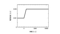
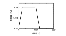
- FIGS. 21 (a) to 21 (c) are diagrams showing simulation results for explaining skyrmion erasing by the applied current. It is a figure which shows the time dependence of the applied current at the time of setting it as 0.002 ⁇ j of the maximum current density used for simulation experiment.
- FIG. 1 is a schematic view showing an example of skirmion which is a nanoscale magnetic structure in a magnetic substance.
- arrows indicate the direction of the magnetic moment.
- Skillmions consist of magnetic moments that point in all directions. When the direction of the magnetic field applied in the magnetic body is upward in the figure, the outermost magnetic moment is upward as well as parallel to the magnetic field as the direction of the magnetic field.
- the skyrmion is in the form of a plane rotating inward in a spiral from its outermost periphery, and along with this, the direction of the magnetic moment gradually changes its direction.
- the nanoscale magnetic structure swirling in the magnetic material is characterized by the skyrmion number.
- the skyrmion number is expressed by the following [Equation 1] and [Equation 2] which indicates how many times the magnetic moment swirls per unit space.
- the polar angle ⁇ (r) with the magnetic moment is a continuous function of the distance r from the center of the skyrmion, and when r is changed from 0 to infinity, from ⁇ to zero or from zero to ⁇ Change.
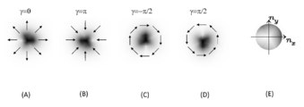
- FIG. 2 is a schematic view showing skillions having different phases.
- FIG. 2E shows how to use the coordinates (right hand system).
- the z-axis is oriented from the back to the front of the drawing with respect to the x-axis and the y-axis.
- the shading indicates the direction of the magnetic moment. Arrows indicate magnetic moments.
- the magnetic structure shown in FIG. 2 is in a state defined as skirmion.
- ⁇ indicates the phase between magnetic moments.
- FIG. 2 four examples (A) to (D) of different phases ⁇ are shown.
- FIGS. 2A to 2D look different, they are topologically identical magnetic structures.
- the skyrmion having such a structure is stably present once generated, and acts as a carrier responsible for signal transmission in the chiral magnetic material under application of an external magnetic field.
- FIG. 3 is a schematic view showing the magnetic element 10 that enables the transfer of the skyrmion according to the first embodiment.
- the magnetic element 10 is an element formed in a thin layer having a thickness of 500 nm or less, and is formed using a technique such as MBE (Molecular Beam Epitaxy) or sputtering.
- the magnetic element 10 includes a thin layer magnetic body 13 made of a chiral magnetic material, an upstream nonmagnetic metal 11 which is a thin layer conductive body connected in the spreading direction of the magnetic body 13, and an upstream nonmagnetic metal 11. And a downstream nonmagnetic metal 12 which is a thin layered conductor connected to the magnetic body 13 at a distance.
- the upstream nonmagnetic metal 11 and the downstream nonmagnetic metal 12 are made of a conductive nonmagnetic metal such as Cu, W, Ti, TiN, Al, Pt, or Au.
- the magnetic body 13 is a chiral magnetic body and is made of FeGe, MnSi or the like.
- the downstream nonmagnetic metal 12 is connected in the spreading direction of the magnetic body 13.
- the connection form of the downstream nonmagnetic metal 12 is not limited to this, and the downstream nonmagnetic metal 12 may be stacked on the magnetic body 13 and connected.
- the power supply 14 is connected to the upstream nonmagnetic metal 11 and the downstream nonmagnetic metal 12. Further, on the lower surface side of the magnetic body 13 of the magnetic element 10 in FIG. 3, a magnetic field generation unit (not shown) is provided to face the magnetic body 13.
- a skirmion memory is configured by including the magnetic element 10, the power supply 14, and a magnetic field generation unit (not shown).
- a magnetic field generation unit applies a magnetic field to the magnetic element 10 in the direction of the arrow B.
- the chiral magnetic material in the magnetic material 13 is a magnetic material whose magnetic moment arrangement when no magnetic field is applied rotates in a spiral with respect to the traveling direction of the magnetic moment.
- the chiral magnetic material becomes a magnetic material that stabilizes skyrmions. If the magnetic field strength is further increased, it becomes ferromagnetic. With respect to a plurality of skirmions generated in this ferromagnetic body, the transfer state of the drive current and the skirmions will be examined.
- R (X, Y) indicates the center position of the magnetic structure.
- Vd is the time derivative of R and indicates the velocity of the magnetic structure. The behavior of this magnetic structure is derived from the equation of motion shown in the following [Equation 3].
- Equation 3 X indicates an outer product.
- V S ⁇ j, indicating the velocity of conduction electrons.
- ⁇ 2eM / (pa 3 ).
- a a lattice constant.
- M is the magnetic moment and p is the spin polarization of conduction electrons.
- the third term F is a force acting on the magnetic structure from the boundary between the electrode and the magnetic body, an impurity, a magnetic field or the like.
- G Ge z in units e z along the z-direction.
- N sk is the number of skill mions.
- the second term shows the dissipation process.
- ⁇ is a Gilbert damping coefficient, and ⁇ is a nonadiabatic process. And ⁇ to ⁇ .
- , Vd Vs.
- the moving speed of the skyrmion is higher than the moving speed of the domain wall.
- ⁇ is 10 2 -10 3 because ⁇ is 10 -2 -10 -3 . This indicates that it is possible to increase the speed of the skyrmion to 100 times to 1000 times the speed of the domain wall.
- the movement speed of the skirmion is 100 times to 1000 times the movement speed of the domain domain wall.
- the orientation relationship between the direction of movement of the skyrmion and the direction of the current flowing from the upstream nonmagnetic metal 11 to the downstream nonmagnetic metal 12 is important.
- the direction of movement of the skyrmion (C direction) and the direction of current (A direction) have been theoretically elucidated in the case where they are arranged in a substantially perpendicular direction.
- this arrangement is called lateral current arrangement.
- longitudinal current arrangement the case where the current direction and the direction of transfer of the skyrmion are arranged in parallel.
- the transfer rate of the skyrmion of the lateral current arrangement is 100 to 1000 times the moving velocity of the domain domain wall, which is the same moving speed as that of the longitudinal current arrangement.
- the magnetic body is not a chiral magnetic body exhibiting a helical magnetic property but a dipole magnetic body, a frustrated magnetic body, or a laminated interface structure of a magnetic material and a nonmagnetic material. be able to.
- a dipole magnetic body is a magnetic body in which magnetic dipole interaction is important.
- the frustrated magnetic material is a magnetic material that includes a magnetic interaction space structure that favors a magnetic mismatch state.
- a magnetic body having a laminated interface of a magnetic material and a nonmagnetic material is a magnetic body in which the magnetic moment in contact with the nonmagnetic material of the magnetic material is modulated by the spin-orbit interaction of the nonmagnetic material.
- Example 1 of First Embodiment The simulation experiment result about the optimal magnetic body width in the transfer method of skyrmion in Example 1 is shown.
- LLG Landau-Lifshitz-Gilbert
- ⁇ g ⁇ B / h (> 0) is the gyromagnetic ratio.
- h Planck's constant.
- M r represents a magnetic moment in a dimensionless amount.
- X indicates the outer product.
- e x and e y are unit vectors in the x and y directions.
- M r + ex and M r + ey indicate magnetic moments at positions different by a unit vector in the x and y directions with respect to M r .
- ⁇ 2eM / (pa 3 ).
- Equation 9 the Hamiltonian H represented by [Equation 9] is the case of a chiral magnetic material.
- the expression of H may be replaced with ones that describe the respective magnetic bodies.
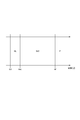
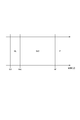
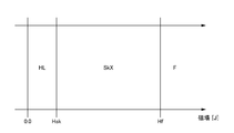
- the experimental conditions of the simulation experiment in the present embodiment are shown in FIG. It is the phase diagram which showed the magnetic field dependence of the chiral magnetic body magnetic phase.
- the chiral magnetic substance is a magnetic substance which changes from the chiral magnetic phase (HL) to the skyrmion phase (SkX) according to the magnetic field strength Hsk, and further changes from the skyrmion phase (SkX) to the ferromagnetic phase (F) at high magnetic field strength Hf.
- HL chiral magnetic phase
- SkX skyrmion phase
- F ferromagnetic phase
- Hsk 0.0075 J.
- a is the lattice constant of the magnetic body 11
- D is the magnitude of the Jaroshinski-Moriya interaction and is a physical constant inherent to the substance. Therefore, the skyrmion diameter ⁇ is a substance specific constant.
- the skyrmion diameter ⁇ is, for example, 70 nm for FeGe and 18 nm for MnSi.
- the simulation experiment results in the present embodiment will be described in detail below.
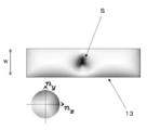
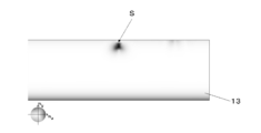
- An appropriate minimum width of the magnetic body 13 for transferring the skillion S is shown in FIG.
- the width W of the magnetic body 13 mentioned here is the width in the vertical direction in the drawing from the upstream nonmagnetic metal 11 to the downstream nonmagnetic metal 12 (hereinafter referred to as the transfer width W).
- the light and shade represented by the n x and n y axes crossing each other in FIGS. 5 to 7 below indicate the directions of the magnetic moments represented on the n x and n y axes.
- the transfer width determines the memory density. Therefore, being able to determine the minimum width of transfer width means that the design rule has been decided, which is important as a design guideline.
- the minimum transfer width is 0.5 of the skyrmion diameter ⁇ .
- Example 2 of First Embodiment In the transfer method of the plurality of skill mions in the second embodiment, the simulation experiment result on the interval d of the plurality of skill mions transferred by the magnetic body 13 is shown.
- the interval d between the skill mions S is 2 ⁇ ⁇ .
- the two skyrmions repel each other due to the magnetic moment of each other, and are eventually separated from each other.
- the magnetic body 13 constituting the memory is sandwiched between the upstream nonmagnetic metal 11 and the downstream nonmagnetic metal 12 to form a skyrmion transfer path of the magnetic body 13.
- a current is applied between the upstream nonmagnetic metal 11 and the downstream nonmagnetic metal 12
- uniform velocity transfer can be realized at an equal interval between the plurality of skirmions.
- the skillion S carrying the bit information can be transferred in the magnetic body 13 on the thin line.
- the lateral current arrangement structure realizes high-speed transfer whose transfer rate is 100 times to 1000 times that of the longitudinal current arrangement.
- the lateral current arrangement can provide a current arrangement that is significantly simpler in structure than the longitudinal current arrangement.
- the distance between the electrodes is long and short, which impairs the control feasibility.
- the skill mions S may be generated so that the interval d between the skill mions S is 2 ⁇ or more.
- the generation interval d of the skyrmion S may be 3 ⁇ to 5 ⁇ .
- the present embodiment can be embodied as a route route method of the skyrmion for designing the skyrmion memory device and is extremely important.
- the transfer method of this skyrmion is expressed as an amount normalized by the amount of magnetic exchange interaction J characterizing the magnetism of the magnetic substance. Therefore, it can be embodied as a transfer method applicable to various chiral magnetic materials, and the application range is wide.
- the effect of the embodiment of the chiral magnetic material described here is qualitatively the same even with a dipole magnetic material, a frustrated magnetic material, or a magnetic material having a laminated interface of a magnetic material and a nonmagnetic material.
- the first embodiment provides design guidelines for the skyrmion transfer method.
- FIG. 8 is a schematic view showing the magnetic element 10 capable of erasing the skyrmion according to the second embodiment.
- the magnetic element 10 is an element formed in a thin layer having a thickness of 500 nm or less, and is formed using a technique such as MBE (Molecular Beam Epitaxy) or sputtering.
- MBE Molecular Beam Epitaxy
- the magnetic element 10 includes a thin layer magnetic body 13 made of a chiral magnetic material, an upstream nonmagnetic metal 11 which is a thin layer conductive body connected in the spreading direction of the magnetic body 13, and an upstream nonmagnetic metal 11. And a downstream nonmagnetic metal 12 which is a thin layered conductor connected to the magnetic body 13 at a distance.
- the upstream nonmagnetic metal 11 and the downstream nonmagnetic metal 12 are made of a conductive nonmagnetic metal such as Cu, W, Ti, TiN, Al, Pt, or Au.
- the magnetic body 13 is a chiral magnetic body and is made of FeGe, MnSi or the like.
- a notch 21 is formed in the magnetic body 13.
- the upstream nonmagnetic metal 11 is in contact with the U-shaped inner peripheral end of the notch 21 in a plan view.
- the distance between the upstream nonmagnetic metal 11 and the downstream nonmagnetic metal 12 becomes narrow, and a narrow transfer path 22 is formed.
- the skirmion 5 is transferred along the narrow transfer path 22 in the C direction.
- the notch 21 In addition to the notch 21 cut from the upstream nonmagnetic metal 11, the notch 21 includes a notch cut from the interface with the downstream nonmagnetic metal 12.
- the downstream nonmagnetic metal 12 is connected in the spreading direction of the magnetic body 13.
- the connection form of the downstream nonmagnetic metal 12 is not limited to this, and the downstream nonmagnetic metal 12 may be stacked on the magnetic body 13 and connected.
- the power supply 14 is connected to the upstream nonmagnetic metal 11 and the downstream nonmagnetic metal 12. Further, on the lower surface side of the magnetic body 13 of the magnetic element 10 in FIG. 8, a magnetic field generation unit (not shown) is provided to face the magnetic body 13.
- a skirmion memory is configured by including the magnetic element 10, the power supply 14, and a magnetic field generation unit (not shown).
- a magnetic field generation unit applies a magnetic field to the magnetic element 10 in the direction of the arrow B.
- the chiral magnetic material in the magnetic material 13 is a magnetic material whose magnetic moment arrangement when no magnetic field is applied rotates in a spiral with respect to the traveling direction of the magnetic moment.
- the chiral magnetic material becomes a magnetic material that stabilizes skyrmions. If the magnetic field strength is further increased, it becomes ferromagnetic. With respect to a plurality of skirmions generated in this ferromagnetic body, the transfer state of the drive current and the skirmions will be examined.
- this embodiment which consists of a structure mentioned above, it embodies as a magnetic element 10 which can erase one or a plurality of skyrmions transferred in the magnetic body 13.
- a magnetic element 10 which can erase one or a plurality of skyrmions transferred in the magnetic body 13.
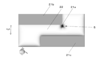
- FIG. 8 when the skyrmion 5 moving in the C direction in the chiral magnetic material in the magnetic body 13 approaches the notch 21, along the side of the notch 21 to the downstream nonmagnetic metal 12 side To be transferred in the transfer path 2 as it is.
- This skill mion 5 can be erased in the process of being transferred within the transfer path 22. That is, in the process of moving the narrow transfer path 22 in the direction of the arrow C, the skyrmion 5 gradually approaches the upstream nonmagnetic metal 11 and the skyrmions 5a, 5b, 5c, and finally this cutting It will erase
- the corner portion 21a has an acute angle or an obtuse angle, and the potential of the magnetic moment is low. By bringing skirmion 5 into contact with such a corner 21a, it becomes possible to erase this by the corner 21a having the low magnetic moment potential.
- the corner 21 a of the notch 21 can be more effectively eliminated from the skyrmion 5 by having a substantially right angle or an acute angle, but it may be an obtuse angle or a rounded shape. Even if it is said, it becomes possible to erase similarly.
- the experimental conditions of the simulation experiment in this embodiment are shown in FIG. It is the phase diagram which showed the magnetic field dependence of the chiral magnetic body magnetic phase.
- the chiral magnetic substance is a magnetic substance which changes from the chiral magnetic phase (HL) to the skyrmion phase (SkX) according to the magnetic field strength Hsk, and further changes from the skyrmion phase (SkX) to the ferromagnetic phase (F) at high magnetic field strength Hf.
- HL chiral magnetic phase
- SkX skyrmion phase
- F ferromagnetic phase
- D 0.18 J
- Hsk 0.0075 J.
- Hsk 0.0075 J.
- ⁇ has a relationship of J
- D and ⁇ 2 ⁇ 2 ⁇ ⁇ J ⁇ a / D.
- the orientation relationship between the direction of movement of the skyrmion in the simulation experiment and the direction of the current flowing from the nonmagnetic electrode is important.
- the direction of movement of the skyrmion and the direction of the current are arranged in a substantially vertical direction (referred to as a lateral current).
- a lateral current a substantially vertical direction
- the elimination of skyrmions is numerically calculated.
- the initial skyrmion transfer state is set to the steady state by the lateral current. In this steady state, the current density applied to the magnetic substance 13 as the chiral magnetic substance is 0.001 ⁇ j flowing substantially perpendicularly to the nonmagnetic electrode, and based on the applied current density, the skyrmion is at a constant speed. Has been transferred.
- n x direction length Lx1 is required than 2 [lambda]. If the length Lx1 in the n x direction is smaller than 2 ⁇ , the transfer path 22 itself is shortened, so that the skill muon 5 transferred on the transfer path 22 is the arrow of the transfer path shown in FIG. As it passes through the lower part of the notch 21.
- Lx in FIG. 11 is an example of 0.5 ⁇ . Further, in the simulation of FIG. 11, the transfer speed of the skirmion is the same as that of FIG.
- the length Lx1 in the n x direction of the notch 21 is not necessarily limited to the case where the above-mentioned conditions are satisfied, and if the transfer speed of the skirmion 5 is higher, Even if Lx1 ⁇ 2 ⁇ , it becomes possible to erase the skill muon 5 at the corner 21a of the notch 21 as described above.
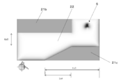
- FIG. 12 is a plan view in the case of forming a trapezoidal notch 21 in the magnetic body 13 with the length of the upper side along the lower end of the upstream nonmagnetic metal 11 of the magnetic body 13 being Lx 1 and the length Lx 2 of the lower side. It is a simulation experiment result about the elimination method of Lumion 5. In the above-described structure, as shown in FIG. 12A, in the case of Skillmion 5 with a slow transfer speed, Skillmion 5 passes without being erased.
- FIG. 12B shows an example where the skillion transfer rate is doubled as compared to the example shown in FIG. 12A.
- the skill transfer 5 having such a high transfer speed, the skill transfer 5 can be erased at the corner 21 a of the notch 21.
- Lx1 is twice as large as the diameter ⁇ of the skyrmion, and Lx2 and Ly1 are equal to ⁇ .
- FIG. 13 shows a simulation experiment result of the erasing method having a trapezoidal notch 21 having the upper side length Lx1 and the lower side length Lx2 along the upstream nonmagnetic metal 11 end of the magnetic body 13.
- the transfer speed of the skirmion is the same, and the length Lx1 of the upper side of the notch 21 is ⁇ .
- the length Lx2 of the lower side of the notch 21 is ⁇ in FIG. 13A, whereas it is 1.2 ⁇ in the example of FIG. 13B.
- the length Lx2 of the lower side becomes long.
- the length Lx2 of the lower side thereof is set long, so that the transmitted skill muon 5 can be erased at the corner 21 a of the notch 21.
- the length Lx2 of the lower side of the trapezoidal cutout 21 needs to have the following relationship with respect to the diameter ⁇ of the skyrmion 5 as a condition for eliminating the skyrmion 5. Lx2> ⁇
- FIG. 14 shows a simulation experiment result in the case where two notches 21 b and 21 c are arranged in the magnetic body 13.
- a transfer path 22 for transferring the skyrmion 5 is formed between the notch 21 b provided from the upstream nonmagnetic metal 11 and the notch 21 c provided from the downstream nonmagnetic metal 12.
- the width of the transfer path 22 is Ly 2
- the following relationship is established between the skyrmion 5 and the diameter ⁇ of the skyrmion 5. Can not enter. Ly2 ⁇
- the skill muon 5 is transferred on the transfer path 22, and is erased at the corner 21a of the notch 21b.
- the notch 21 b on the upstream nonmagnetic metal 11 side has a rectangular shape
- the notch 21 c on the downstream nonmagnetic metal 12 side Shows an example of a trapezoidal shape.
- the length of the lower side of the trapezoidal cutout 21c Lx3 is a 4.lamda
- n x direction length of the slope provided toward the upper side from the lower side is set to 2 [lambda].
- the length Lx4 in the figure is 2 ⁇ .
- the transfer path 22 between the notch 21 b and the notch 21 c is configured to be gradually narrowed in width according to the transfer direction of the skyrmion 5.
- FIGS. 17A to 17H show configuration examples of the notch 21 formed in the magnetic body 13 in the magnetic element 10 to which the present embodiment is applied.
- the notch 21 may have a triangular shape, a square shape, other polygonal shapes, a key shape, a semicircular shape, a semielliptical shape, or any other shape without being limited to the form of FIG. Of course it is also good.
- the present embodiment can be embodied as a method of erasing the skyrmion for designing the skyrmion memory device, and is extremely important.
- This skyrmion elimination method is expressed as an amount normalized by the amount of magnetic exchange interaction J characterizing the magnetism of the magnetic substance. Therefore, it can be embodied as an elimination method applicable to various chiral magnetic materials, and the application range is wide.
- the effect of the embodiment of the chiral magnetic material described herein is qualitatively whether it is a dipole magnetic material, a frustrated magnetic material, or a lamination of a magnetic material and a nonmagnetic material. Even if it is a magnetic body which consists of a structure, it plays similarly.
- the present embodiment provides a design guideline for the skyrmion elimination method.
- FIG. 18 is a schematic view showing the magnetic element 10 which enables the transfer of skill ions according to the third embodiment.
- the magnetic element 10 is an element formed in a thin layer having a thickness of 500 nm or less, and is formed using a technique such as MBE (Molecular Beam Epitaxy) or sputtering.
- the magnetic element 10 includes a thin layer magnetic body 13 made of a chiral magnetic material, an upstream nonmagnetic metal 11 which is a thin layer conductive body connected in the spreading direction of the magnetic body 13, and an upstream nonmagnetic metal 11. And a downstream nonmagnetic metal 12 which is a thin layered conductor connected to the magnetic body 13 at a distance.
- the upstream nonmagnetic metal 11 and the downstream nonmagnetic metal 12 are made of a conductive nonmagnetic metal such as Cu, W, Ti, TiN, Al, Pt, or Au.
- the magnetic body 13 is a chiral magnetic body and is made of FeGe, MnSi or the like.
- the downstream nonmagnetic metal 12 is connected in the spreading direction of the magnetic body 13.
- the connection form of the downstream nonmagnetic metal 12 is not limited to this, and the downstream nonmagnetic metal 12 may be stacked on the magnetic body 13 and connected.
- the power supply 14 is connected to the upstream nonmagnetic metal 11 and the downstream nonmagnetic metal 12. Further, on the lower surface side of the magnetic body 13 of the magnetic element 10 in FIG. 18, a magnetic field generation unit (not shown) is provided to face the magnetic body 13.
- a skirmion memory is configured by including the magnetic element 10, the power supply 14, and a magnetic field generation unit (not shown).
- a magnetic field generation unit applies a magnetic field to the magnetic element 10 in the direction of the arrow B.
- the chiral magnetic material in the magnetic material 13 is a magnetic material whose magnetic moment arrangement when no magnetic field is applied rotates in a spiral with respect to the traveling direction of the magnetic moment.
- the chiral magnetic material becomes a magnetic material that stabilizes skyrmions. If the magnetic field strength is further increased, it becomes ferromagnetic. With respect to a plurality of skirmions generated in this ferromagnetic body, the transfer state of the drive current and the skirmions will be examined.
- the skyrmion 5 moving in the chiral magnetic material in the magnetic material 13 is not limited as long as the magnetic material 13 is between the upstream nonmagnetic metal 11 and the downstream nonmagnetic metal 12. Can be erased. That is, in the process of moving in the direction of the arrow C, the skyrmion 5 gradually approaches the upstream nonmagnetic metal 11 with the skyrmions 5a, 5b, 5c, and is finally erased.
- the method of eliminating the skill mions will be described through examples.
- Example 1 of Third Embodiment The simulation experiment result of transfer and elimination of skyrmion in Example 1 is shown. The skillion movement was described above using [Equation 8] and [Equation 9]. In this simulation, the equations shown in [Equation 8] and [Equation 9] were solved numerically and executed.
- the experimental conditions of the simulation experiment in this embodiment are shown in FIG. It is the phase diagram which showed the magnetic field dependence of the chiral magnetic body magnetic phase.
- the chiral magnetic substance is a magnetic substance which changes from the chiral magnetic phase (HL) to the skyrmion phase (SkX) according to the magnetic field strength Hsk, and further changes from the skyrmion phase (SkX) to the ferromagnetic phase (F) at high magnetic field strength Hf.
- HL chiral magnetic phase
- SkX skyrmion phase
- F ferromagnetic phase
- D 0.18 J
- Hsk 0.0075 J.
- Hsk 0.0075 J.
- the orientation relationship between the direction of movement of the skyrmion in the simulation experiment and the direction of the current flowing from the nonmagnetic electrode is important.
- the direction of movement of the skyrmion and the direction of the current are arranged in a substantially vertical direction (referred to as a lateral current). In the case of such an arrangement, the elimination of skyrmions is numerically calculated.
- the time change of the transverse current application in the simulation experiment is shown in FIG.
- the initial skyrmion transfer state is set to the steady state by the lateral current.
- the current density applied to the magnetic substance 13 as the chiral magnetic substance is 0.001 ⁇ j flowing substantially perpendicularly to the nonmagnetic electrode, and based on the applied current density, the skyrmion is at a constant speed. Has been transferred.
- the drive current is increased between the upstream nonmagnetic metal 11 and the downstream nonmagnetic metal 12 via the power supply 14.
- the start point of increase of the drive current is 0 (1 / J) in the horizontal axis (time; 1 / J) in FIG. 20, 0.002 ⁇ j by time 1000 ((1 / J) starting from this.
- increase the current density and keep the current density at 0.002 ⁇ j for a time of 1000 to 11000 (1 / J) Under such conditions, use [Equation 8] and [Eq. The calculation was carried out.
- FIG. 21 shows the result of a simulation regarding the elimination of skyrmion S.
- FIG. 21A shows a steady state, in which the skyrmions S move in the direction of C inside the magnetic body 13 under a current density of 0.001 ⁇ j.
- the shading represented by the n x and n y axes crossing each other in FIGS. 23, 25, 27, 29, and 31 below indicates the direction of the magnetic moment represented on the n x and n y axes. There is.
- the state of skill mion S at time 8000 (1 / J) is shown in FIG. As shown in FIG. 21B, the skirmion S approaches the vicinity of the interface between the magnetic body 13 and the upstream nonmagnetic metal 11 while being transferred in the C direction.
- FIG. 11 The state of the skillmion S at time 11000 (1 / J) is shown in FIG. It shows a state in which the current density is maintained at 11000 (1 / J) after the current density is set to 0.002 ⁇ j. Skirmions S approaching the upstream nonmagnetic metal 11 are erased from the magnetic body 13 as if absorbed by the upstream nonmagnetic metal 11.
- the current from the upstream nonmagnetic metal has two effects on skirmion.
- One is the lateral current effect on skirmion as described above.
- the other is the attraction effect on the skyrmion on the upstream nonmagnetic metal 11.
- the transverse current effect on the skyrmion produces an effect of laterally accelerating the skyrmion on the magnetic material.
- the attraction effect on the skyrmion works to overcome the potential wall between the upstream nonmagnetic metal 11 and the magnetic body 13.
- the threshold of the current density that can cancel the skyrmion depends on the skyrmion speed to be transferred.
- the time taken for erasing also depends on the transfer speed of skillion.
- Example 2 of the Third Embodiment With the current density set to 0.002 ⁇ j, the time-dependence of applied current is shown in FIG. 22 and FIG.
- the applied current density was set to 0.002 ⁇ j and the application time was set to 6000 (1 / J) as shown in FIG. 22
- both of the skyrmions S could be erased as shown in FIG.
- FIG. 24 when the application time of the current density 0.002 ⁇ j is 5000 (1 / J), it was found that both of the skyrmions S can not be erased as shown in FIG. In this case, it can be seen that the gap between the two skill mions S also increases. Therefore, it is understood that, in the case of a current density of 0.002 ⁇ j, it is necessary to continue applying the application time of 6000 (1 / J) or more.
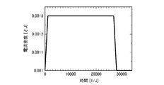
- FIG. 27 shows the state of skyrmion S under the simulation conditions shown in FIG.
- FIG. 27 (a) shows the state of two skyrmions S in the magnetic substance 13 when the application time is 0 (1 / J).
- FIG. 27B shows the state of two skyrmions S in the magnetic substance 13 at time 27000 (1 / J). At time 27000 (1 / J), two skyrmions S in the magnetic body 13 can be erased.
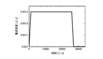
- FIG. 29 shows the state of skyrmions S in the magnetic body 13 at an application time of 26000 (1 / J) under the simulation conditions shown in FIG. As shown in FIG. 29, one skill mion S remains unerasable.
- FIG. 31 shows the state of skyrmions S in the magnetic body 13 at an application time of 25000 (1 / J) under the simulation conditions shown in FIG. As shown in FIG. 31, even one can not be erased anymore and both remain. From the above results, it was found that when the current density is set to 0.0013 ⁇ j, the current application time is required to be 27000 (1 / J) or more in order to erase two or more skirmions S.
- the number of skill mions that can be erased is any number of one or more.
- the magnitude of the current density for erasing depends on the transferred skillion rate.
- the application time for erasing depends on the current density. When the current density is large, the application time may be short, but when the current density is small, the application time needs to be extended.
- the skyrmion S may be erased collectively.
- the width of the magnetic body 13 is temporarily not less than 1/2 ⁇ and less than ⁇ of the diameter ⁇ of the skyrmion S, the skyrmion S can be collectively erased even if the current density is less than 0.0013 J. is there.
- the present embodiment is not limited to the case where the value is constantly maintained until the application time thereafter after the steady state is increased to the current density, and the current density may be reduced halfway Also have similar effects.
- the skyrmion elimination method by current application has been described in the embodiments.
- the skyrmion erasing method by the increase of the current density can perform batch erasing on a designated region in the magnetic body 13.
- the upstream nonmagnetic metal 11 and the downstream nonmagnetic metal 12 are provided on both sides of the designated region in the magnetic body 13 on both sides of the designated region, and the upstream nonmagnetic metal 11 and the downstream nonmagnetic metal 12 are provided.
- Batch erase can be performed for a plurality of skill mions S flowing between them.
- the present invention is also applicable to the case of collectively erasing the entire memory.
- the erasing current is supplied to the entire area by sandwiching the entire magnetic body 13 constituting the memory with the upstream nonmagnetic metal 11 and the downstream nonmagnetic metal 12. It is possible to realize batch erase of the entire memory. As a result, all the skill ions in the memory can be erased in a short time, and the bit information to which the skill ions are assigned can also be erased at once in a batch, so that the erasing time can be shortened and made efficient. it can.
- the storage element having the above-described configuration in which the skill mions are allocated as bit information, is used as a hard disk (HD)
- HD hard disk
- the magnetic material 13 in the erased track region may be configured to be capable of applying a current of high current density to the upstream nonmagnetic metal 11 and the downstream nonmagnetic metal 12.
- the present embodiment can be embodied as a skyrmion erasing method for designing a skyrmion memory device and is extremely important.
- This skyrmion elimination method is expressed as an amount normalized by the amount of magnetic exchange interaction J characterizing the magnetism of the magnetic substance. Therefore, it can be embodied as an elimination method applicable to various chiral magnetic materials, and the application range is wide.
- the effect of the embodiment of the chiral magnetic material described herein is qualitatively whether it is a dipole magnetic material, a frustrated magnetic material, or a lamination of a magnetic material and a nonmagnetic material. Even if it is a magnetic body which consists of a structure, it plays similarly.
- the present embodiment provides design guidelines for the skyrmion elimination method, in particular the skyrmion batch elimination method.
- Skill Mion is allocated as bit information, this skill memory memory can perform this writing and erasing any number of times. And there is no limitation on the number of writes and the number of erasures of this skill mion. That is, it can be said that the skill mion memory has endless endurance (durability). Skirmion memory can significantly improve data retention performance. These two features in the skyrmion memory can be said to solve at once the problems such as the limitation of the number of times of writing of electron storage in the flash memory utilizing the insulation property of the oxide film and the deterioration of the retention performance.
- FIG. 32 is a schematic view showing an example of the apparatus 100 on which the skill mion memory 110 is mounted.
- the apparatus 100 includes processing units such as a skill-ion memory 110 and a processor 140.
- the skyrmion memory 110 has the magnetic element 10, the power supply 14 and the magnetic field generation unit described with reference to FIG.
- the processing unit exchanges data with the skill meon memory 110.
- the processing unit may process the data read from the skill muon memory 110.
- the apparatus 100 is, for example, a CMOS-LSI device equipped with skirmion memory as an example.
- a CMOS-LSI device is provided as the processing unit.
- the CMOS-LS device and the magnetic element 10 of the skyrmion memory 110 may be provided in the same chip.
- the device 100 may also be a personal computer, data recording medium, data recording device, mobile phone, smart phone, digital camera, stick memory, communication device, image recording device, television receiver, self-propelled device, flight device, or space. It may be a flight device.
- Skirmion is an ultrafine structure having a nanoscale size with a diameter of 1 to 100 nm, and can be applied as a large-capacity storage magnetic element capable of extremely densifying enormous bit information.
- the skyrmion memory and the CMOS-LSI device may be embodied as a CMOS-LSI device with the skyrmion memory formed in the same chip.
- the skyrmion can electrically transfer, erase or batch erase bit information to be assigned to it. Then, the transfer time and the erase time of the bit information related to this skill mion can be realized in nanoseconds through the present invention.
- By realizing a high-speed large-scale non-volatile memory based on such skyrmion it is expected to be utilized as a memory that greatly improves the high-speed processing capability of large-scale information required for many electronic devices at present.
- the recording method of Skirmion memory transferred at high speed by current is an electronic device such as a hard disk (HD) which is a large capacity magnetic memory. Not only can eliminate the motor drive load, but also ultra-high-speed writing and erasing are possible. For this reason, the skyrmion memory is likely to replace the current data storage device such as a hard disk in the future. Further, in a flash memory capable of electrically transferring and erasing information, a magnetic element to which the present invention is applied exhibits many advantages, particularly while a large-capacity recording capacity in recent years is required. Is possible.
- the magnetic element to which the present invention is applied uses the magnetic moment as the recording means, the recording and holding state can be held in a long and stable state.
- the magnetic element to which the present invention is applied can shorten the erase operation time as much as possible, and the time can be shortened to nanoseconds. As a result, it is possible to realize an erase operation time equivalent to that of a DRAM.
- the above-described skillion memory to which the present invention is applied to an electronic device it is possible to significantly improve the use environment. Specifically, it is possible to realize shortening of the rise time from power-on to the electronic device to operation becoming possible and improvement of response speed, and to provide the user with a comfortable use environment.
- any electronic device may be used, including a personal computer, an image recording device, and the like.
- a magnetic element to which the present invention is applied to a communication device mobile phone, smart phone, tablet terminal, etc.
- image information is taken in and operations of various large-scale application programs are further improved.
- the high-speed implementation and the high-speed responsiveness make it possible to secure a comfortable operating environment for the user.
- speeding up of image display to be displayed on the screen can be realized, it is possible to further improve the use environment.
- the magnetic element to which the present invention is applied to an electronic device such as a digital camera, it is possible to record a moving image over a large volume.
- an electronic device such as a 4K television receiver
- the present invention may be embodied as a data recording medium in addition to the case of being applied to a data recording apparatus such as a hard disk.
- the present invention can be expected to have a great impact on the practical use of a self-propelled device, a flight device, and a space flight device. That is, complex control processing of flight devices, weather information processing, enhancement of services for passengers by providing images with high-definition image quality, control of space flight devices, and recording of vast recorded information of observed image information Bring much knowledge to civilization.
- This skyrmion memory is a memory that has the potential as a high-speed large-scale non-volatile memory and a memory that contributes a great deal to our living environment. Also, skill mions may be applied as a stick memory.
Landscapes
- Engineering & Computer Science (AREA)
- Computer Hardware Design (AREA)
- Hall/Mr Elements (AREA)
- Mram Or Spin Memory Techniques (AREA)
- Thin Magnetic Films (AREA)
Abstract
スキルミオンを転送可能な薄層状の磁気素子であって、薄層状の磁性体13と、磁性体13の延展方向に接続された薄層状の導電体である上流側非磁性金属11と、上流側非磁性金属11と離間して磁性体13に接続された薄層状の導電体である下流側非磁性金属12とを備え、上流側非磁性金属11と下流側非磁性金属12との間に電流を印加することにより、1又は複数のスキルミオンSを転送することを特徴とする。
Description
本発明は、スキルミオンを高速に転送、消去、または、一括消去できる磁気素子及びこの磁気素子を応用したスキルミオンメモリ、スキルミオンメモリ搭載CMOS-LSIデバイス、パーソナルコンピュータ、データ記録媒体、データ記録装置、携帯電話機、スマートフォン、デジタルカメラ、スティックメモリ、通信装置、画像記録装置、テレビジョン受像機、自走装置、飛行装置、宇宙空間飛行装置に関する。
近年において、メモリ等の記録用デバイスの記憶容量に対して大容量化への要求が特に高まっている。例えば画像素子の画素ピッチがより繊細になるにつれて画素数が増大し、これに応じて記録用デバイスに要求される記憶容量は1Mビット相当となる。このような画像素子上で動画を表示させる場合には、1Gビットを超える情報量となるため、当然これに応じた記憶容量が必要となり、記憶用デバイスの記憶容量も1テラビットからさらに大容量化しつつある。またデジタルカメラ等に装着される各種SDメモリカードの大容量化も進行中である。
磁性体の磁気モーメントをデジタル情報として利用する磁気素子は、情報保持時に電力を要さない不揮発性メモリを担うナノスケールの磁気構造による超高密度性等の利点から大容量情報記憶媒体としての応用が期待され、エレクトロニクスデバイスのメモリデバイスとして、その重要度が増している。
さらに近年、不揮発性メモリをシリコン基板上に作られたCMOSデバイスに搭載し、計算処理能力の飛躍的向上を目的とした磁気メモリCMOS混載の研究開発が精力的に行われている。
これは、CMOS回路で構成されたシリコンチップと不揮発性素子チップとの信号のやり取りに伴う、制御回路の省略、制御時間の短縮を目的としたもので、計算処理時間を飛躍的に向上させる技術である。
さらに、この研究開発は、無駄な回路部分への電力を遮断した超省電力デバイスの開発も目的としている。特に近年はCMOS-LSIデバイスの省電力化が重要な課題として浮上しており、待機電力の省力化課題の重要性は増している。
これが実現すると、大規模情報が扱え、その応答は高速で、高機能で人間にやさしいヒューマンインターフェイスをもちなおかつ低消費電力のパーソナルコンピュータ、データ記録媒体、データ記録装置、携帯電話機、スマートフォン、デジタルカメラ、スティックメモリ、通信装置、画像記録装置、テレビ、自走装置、飛行装置、宇宙空間飛行装置などの大容量メモリとして応用展開が期待できる。
こうした状況下で、本願発明者らは、外部磁場のもとでカイラル磁性体にスキルミオン磁気構造をもつ材料を見出し尚かつ電流によりスキルミオンを駆動できることを見出し、この磁気構造体を用いた磁気素子を提案した(特許文献1)。
スキルミオンは中心部において印加された磁場に対して反平行の磁気モーメントを有し、周辺部においては印加された磁場に対して平行な磁気モーメントを有する、渦巻状の磁気構造を備えている。
スキルミオンは、直径が1~100nmのナノスケールサイズの磁気構造を有し、膨大なビット情報を極細密化して記憶できる大容量記憶磁気素子として応用することが期待されている。また、スキルミオンは、このビット情報を直接転送し、情報演算や伝達に応用できる可能性をもつ磁気構造体でもある。
こうした特徴から、スキルミオン素子は、要求される記憶容量が増加の一途をたどるデータ記録媒体およびデータ記録装置用磁気メモリの性能限界にブレークスルーを与える次世代型磁気メモリデバイスの根幹を担うものとして期待されている。
特に磁気メモリは宇宙空間での各種の素粒子や放射線への耐性が強い。スキルミオンメモリも同じ特徴を有している。モーターなどの回転機構を必要としない大容量磁気メモリは宇宙空間におけるメモリの主役としての位置を占めると期待される。
一方で、最近メモリ媒体として浮上している電子を記憶ビットとして利用するフラッシュメモリはこのような環境には適さない。電子は高エネルギー素粒子や放射線によりシリコン酸化膜のエネルギー障壁を簡単に乗り越え、データの消去や誤書き込みを発生させるからである。
また、大規模不揮発性スキルミオンメモリが大規模論理CMOS-LSIデバイスとチップが一体化されると、低消費電力型CMOSデバイスや高インテリジェント型CMOSデバイスにとって大変魅力的であり、こうした技術を応用した高密度不揮発性スキルミオンメモリ混載CMOS-LSIデバイスの登場が期待されている。
次世代型のメモリデバイスの他の候補としては、米国IBMを中心に磁気ドメイン磁壁を駆動してその磁気モーメント配置を電流で転送し、記憶情報を読み出すマグネチックシフトレジスタ1が提案されている(特許文献2参照)。
図33は、電流による磁気ドメイン磁壁駆動の原理を示す模式図である。互いに磁気モーメントの向きが相反する磁気領域の境界がドメイン磁壁である。矢印の向きの電流により磁気ドメイン磁壁が駆動される。ドメイン磁壁が移動することによりドメインを構成する情報を記憶した磁気モーメントの向きによる磁気変化を下部の磁気センサ2で検知して磁気情報を引き出す。
しかし、こうしたマグネチックシフトレジスタ1は、磁気ドメイン磁壁を動かす際に大きな電流が必要であり、また磁気ドメイン磁壁の転送速度が遅いという欠点を持っている。この結果、メモリの書き込み、消去時間が遅くなる。
そこで、本願発明者は、磁性体中に発生するスキルミオンを記憶単位として使ったスキルミオン磁気素子を提案した(特許文献1参照)。この提案において本願発明者らは、スキルミオンを電流により駆動できることを示した。
従来、特定の形状をしたパーマロイなどの材料のエッジに磁気バブルを固定するとともに、磁界を回転させることにより、磁気バブルをエッジ上に動かしていた。すなわち、磁気バブルを用いた磁気素子メモリでは、常に回転磁界が必要となっていた。
これに対して、本願発明者らは、磁気バブルではなくスキルミオンを用いるとともに、これを回転磁界ではなく電流で直接駆動できることを示した。
このように、スキルミオンは電流による転送が可能であることから、磁気情報を直接電流で制御できる磁気素子としての応用が期待されている。
[先行技術文献]
[特許文献]
[特許文献1]特願2012-232324
[特許文献2]米国特許第6834005号
[非特許文献]
非特許文献1 永長 直人、十倉 好紀、"Topological properties and dynamics of magnetic skyrmions"、Nature Nanotechnology、英国、Nature Publishing Group、2013年12月4日、Vol.8、p899-911.
[先行技術文献]
[特許文献]
[特許文献1]特願2012-232324
[特許文献2]米国特許第6834005号
[非特許文献]
非特許文献1 永長 直人、十倉 好紀、"Topological properties and dynamics of magnetic skyrmions"、Nature Nanotechnology、英国、Nature Publishing Group、2013年12月4日、Vol.8、p899-911.
上述したように、メモリや論理演算等のデバイスにスキルミオンを応用することへの期待が高まっているが、スキルミオンの駆動電流とスキルミオンの転送の関係等の詳細が明らかではなかったため、スキルミオンメモリを実現することができない状況であった。
そこで、本願発明者はスキルミオンの駆動電流とスキルミオンの転送状態の関係の詳細を明らかにした上で、1または複数のスキルミオンを高速に転送、消去または一括消去できる磁気素子及びスキルミオンメモリを発明した。
また、こうした磁気素子及びスキルミオンメモリの一つの実施形態においては、所定のトラック領域の1または複数のスキルミオンを印加した電流で高速に転送できることが好ましい。また、こうした磁気素子及びスキルミオンメモリの一つの実施形態においては、1または複数のスキルミオンを印加した電流で所定の箇所において消去できることが好ましい。また、こうした磁気素子及びスキルミオンメモリの一つの実施形態においては、印加した電流で所定のトラック領域のスキルミオンを一括で消去できることが好ましい。
すなわち、本願発明は、低消費電力で1または複数のスキルミオンを高速に転送、消去、または、一括消去できる磁気素子及びこの磁気素子が応用されたスキルミオンメモリ、スキルミオンメモリ搭載CMOS-LSIデバイス、パーソナルコンピュータ、データ記録媒体、データ記録装置、携帯電話機、スマートフォン、デジタルカメラ、スティックメモリ、通信装置、画像記録装置、テレビジョン受像機、自走装置、飛行装置、宇宙空間飛行装置を提供することを目的とする。
本発明の第1の形態においては、スキルミオンを転送可能な薄層状の磁気素子であって、薄層状の磁性体と、磁性体の延展方向に接続された薄層状の導電体である上流側非磁性金属と、上流側非磁性金属と離間して磁性体に接続された薄層状の導電体である下流側非磁性金属とを備え、上流側非磁性金属と下流側非磁性金属との間に電流を印加することにより、1又は複数のスキルミオンが転送されることを特徴とする磁気素子。
磁性体における上流側非磁性金属から下流側非磁性金属に至る幅wは、スキルミオンの直径をλとしたとき、w≧0.5λであってよい。磁性体は、転送される複数のスキルミオンの間隔dがスキルミオンの直径λの2倍以上である場合に、その間隔dを保持しつつスキルミオンを転送してよい。
本発明の第2の形態においては、第1の形態に係る磁気素子と、磁気素子の上流側非磁性金属及び下流側非磁性金属に接続され、上流側非磁性金属から下流側非磁性金属に向けて電流を印加する電源と、磁性体の一面側に対向して設けられた磁場発生部とを備え、電源は、上流側非磁性金属と下流側非磁性金属との間に電流を印加することにより、1又は複数のスキルミオンを転送することを特徴とするスキルミオンメモリを提供する。
磁性体における上流側非磁性金属から下流側非磁性金属に至る幅wは、スキルミオンの直径をλとしたとき、w≧0.5λであってよい。磁性体は、転送される複数のスキルミオンの間隔dがスキルミオンの直径λの2倍以上である場合に、その間隔dを保持しつつスキルミオンを転送してよい。下流側非磁性金属は、磁性体の延展方向に接続されてよい。下流側非磁性金属は、磁性体に積層されて接続されてよい。
本発明の第3の形態においては、スキルミオンを転送可能な薄層状の磁気素子であって、薄層状で切り欠けを有する磁性体と、磁性体の延展方向に接続された薄層状の導電体である上流側非磁性金属と、上流側非磁性金属と離間して磁性体に接続された薄層状の導電体である下流側非磁性金属とを備え、上流側非磁性金属と下流側非磁性金属との間に電流を印加することにより、磁性体中で転送される1又は複数のスキルミオンが、切り欠けを介して消去されることを特徴とする磁気素子を提供する。
磁性体は、上流側非磁性金属に接する磁性体の端部から切り欠けが設けられ、当該切り欠けの内周端に上流側非磁性金属を接触させてよい。磁性体は、切り欠けの隅部においてスキルミオンを消去してよい。磁性体は、上流側非磁性金属に接する磁性体の端部から長方形状の切り欠けが設けられ、切り欠けは、電流の印加方向に対する略直交方向の長さLxが、スキルミオンの直径λの2倍以上であってよい。
磁性体は、上流側非磁性金属に接する磁性体の端部から下流側非磁性金属側に向けて縮径化する台形状の切り欠けが設けられ、切り欠けにおける下流側非磁性金属側により近い下辺の長さLx2は、スキルミオンの直径λより大きくてよい。切り欠けと下流側非磁性金属との間に形成される転送経路の幅、又は複数の切り欠け間に形成される転送経路の幅は、スキルミオンの直径λ以上であってよい。
本発明の第4の形態においては、第3の形態に係る磁気素子と、磁気素子の上流側非磁性金属及び下流側非磁性金属に接続され、上流側非磁性金属から下流側非磁性金属に向けて電流を印加する電源と、磁性体の一面側に対向して設けられた磁場発生部とを備え、電源は、上流側非磁性金属と下流側非磁性金属との間に電流を印加することにより、磁性体中で1又は複数のスキルミオンを、切り欠けを介して消去することを特徴とするスキルミオンメモリを提供する。
下流側非磁性金属は、磁性体の延展方向に接続されていてよい。下流側非磁性金属は、磁性体に積層されて接続されていてよい。
本発明の第5の形態においては、スキルミオンを転送可能な薄層状の磁気素子であって、薄層状の磁性体と、磁性体の延展方向に接続された薄層状の導電体である上流側非磁性金属と、上流側非磁性金属と離間して磁性体に接続された薄層状の導電体である下流側非磁性金属とを備え、上流側非磁性金属と下流側非磁性金属との間に電流を印加することにより、磁性体中で転送される1又は複数のスキルミオンが消去されることを特徴とする磁気素子を提供する。
磁性体中でスキルミオンを転送する際に印加される電流よりも大きな電流を印加することにより、磁性体中で転送される1又は複数のスキルミオンを一括して消去してよい。
本発明の第6の形態においては、第5の形態に係る磁気素子と、磁気素子の上流側非磁性金属及び下流側非磁性金属に接続され、上流側非磁性金属から下流側非磁性金属に向けて電流を印加する電源と、磁性体の一面側に対向して設けられた磁場発生部とを備え、電源は、上流側非磁性金属と下流側非磁性金属との間に電流を印加することにより、磁性体中で転送される1又は複数のスキルミオンを消去することを特徴とするスキルミオンメモリを提供する。
電源は、磁性体中でスキルミオンを転送する際に印加される電流よりも大きな電流を印加することにより、磁性体中で転送される1又は複数のスキルミオンを一括して消去してよい。下流側非磁性金属は、磁性体の延展方向に接続されてよい。下流側非磁性金属は、磁性体に積層されて接続されてよい。
第1から第6の形態において、磁性体は、カイラル磁性体、ダイポール磁性体、フラストレート磁性体、および、磁性材料と非磁性材料との積層界面構造のうちのいずれかからなってよい。
本発明の第7の形態においては、上記形態に係るスキルミオンメモリとCMOS-LSIデバイスが同一チップ内に形成されていることを特徴とするスキルミオンメモリ搭載CMOS-LSIデバイスを提供する。
本発明の第8の形態においては、上記形態に係るスキルミオンメモリを搭載したことを特徴とするパーソナルコンピュータ、データ記録媒体、データ記録装置、携帯電話機、スマートフォン、デジタルカメラ、スティックメモリ、通信装置、画像記録装置、テレビジョン受像機、自走装置、飛行装置および宇宙空間飛行装置を提供する。
上述した構成からなる本発明によれば、低消費電力で1または複数のスキルミオンを高速に転送、消去、または、一括消去できる磁気素子とすることができる。また、この磁気素子が応用されたスキルミオンメモリ、スキルミオンメモリ搭載CMOS-LSIデバイス、およびスキルミオンメモリを内蔵した、パーソナルコンピュータ、データ記録媒体、データ記録装置、携帯電話機、スマートフォン、デジタルカメラ、スティックメモリ、通信装置、画像記録装置、テレビジョン受像機、自走装置、飛行装置、宇宙空間飛行装置を提供することができる。
以下、本発明の実施の形態について、図面を参照して説明する。
図1は、磁性体中のナノスケール磁気構造体であるスキルミオンの一例を示す模式図である。図1において、矢印は磁気モーメントの向きを示している。
スキルミオンは、あらゆる向きを向く磁気モーメントで構成されている。磁性体中に印加される磁場の向きが図中上向きである場合に、最外周磁気モーメントは、その磁場の向きと同様に上向きで、かつ磁場と平行とされている。
スキルミオンは、その最外周から渦巻状に内側へ向けて回転していく平面形態とされ、これに伴って磁気モーメントの向きは徐々に向きを変えることとなる。
そしてスキルミオンの中心を構成する磁気モーメントは、磁場と反平行となるように、下向きで安定することとなる。
スキルミオンでは、磁気モーメントが中心から最外周に至るまで下向きから上向きに連続的に遷移しつつ規則的に並ぶ結果、複数の磁気モーメントが渦のように規則的に並んだ構造をしている。中心の磁気モーメントと最外周の磁気モーメントの向きは反平行で、中心から外周の間に向きは連続的にねじれ、渦巻き構造を形成する。
ここで、磁性体中に渦巻くナノスケール磁気構造体は、スキルミオン数で特徴づけられる。スキルミオン数は、単位空間あたり何回磁気モーメントが渦巻くかを示す、以下の[数1]及び[数2]で表現される。[数2]において、磁気モーメントとの極角Θ(r)はスキルミオンの中心からの距離rの連続関数であり、rを0から無限まで変化させたとき、πからゼロもしくはゼロからπに変化する。


このようなスキルミオン数Nsk=-1の場合の一例を図2に示した。図2は、位相が異なるスキルミオンを示す模式図である。図2(E)は座標のとりかた(右手系)を示している。x軸、y軸に対してz軸は紙面の裏から手前の向きに向けて設ける。濃淡は磁気モーメントの向きを示している。矢印は磁気モーメントを示している。この図2に示す磁気構造体は、スキルミオンと定義される状態にある。
γは磁気モーメント間の位相を示している。図2では、異なる位相γの4例(A)~(D)が示されている。
(A)γ=0に対して(B)γ=πのすべての磁気モーメントの向きは丁度180°回転した磁気モーメントの向きを持っている。この時の濃淡と磁気モーメントの向きは(E)での定義に対応している。
(C)γ=-π/2はγ=0のすべての磁気モーメントの向きに対し、-90度(右回りに90度)の磁気モーメントの向きをとる。なお、図2(D)の位相λ=π/2のスキルミオンが、図1のスキルミオンに相当する。
すなわち、図2(A)~(D)に図示した4例の磁気構造は異なるように見えるが、トポロジー的には同一の磁気構造体である。
このような構造を有するスキルミオンは、一度生成すると安定して存在し、外部磁場印加下のカイラル磁性体中で情報伝達を担うキャリアとして働く。
次に、このようなスキルミオン数Nsk=-1のナノスケール磁気構造体であるスキルミオンの運動を以下に記述する。
[第1の実施形態]
図3は、第1の実施形態に係るスキルミオンの転送を可能とする磁気素子10を示す模式図である。磁気素子10は、厚さが500nm以下の薄層状に形成された素子であり、MBE(Molecular Beam Epitaxy)やスパッター等の技術を用いて形成されている。
図3は、第1の実施形態に係るスキルミオンの転送を可能とする磁気素子10を示す模式図である。磁気素子10は、厚さが500nm以下の薄層状に形成された素子であり、MBE(Molecular Beam Epitaxy)やスパッター等の技術を用いて形成されている。
磁気素子10は、カイラル磁性体よりなる薄層状の磁性体13と、磁性体13の延展方向に接続された薄層状の導電体である上流側非磁性金属11と、上流側非磁性金属11と離間して磁性体13に接続された薄層状の導電体である下流側非磁性金属12と、を備えて構成されている。
上流側非磁性金属11及び下流側非磁性金属12は、Cu、W、Ti、TiN、Al、Pt、Au等の導電性の非磁性金属よりなる。
磁性体13はカイラル磁性体であり、FeGeやMnSi等よりなる。
本実施形態においては、下流側非磁性金属12は、磁性体13の延展方向に接続されている。しかし、下流側非磁性金属12の接続形態はこれに限らず、下流側非磁性金属12を、磁性体13に積層して接続する態様としてもよい。
この磁気素子10を用いてスキルミオンを転送させる際には、上流側非磁性金属11及び下流側非磁性金属12に電源14が接続される。また、磁気素子10の磁性体13の図3における下面側には、磁性体13に対向して図示しない磁場発生部が設けられる。この磁気素子10、電源14及び図示しない磁場発生部を備えてスキルミオンメモリが構成されている。
電源14から上流側非磁性金属11に電流が印加されると、電流は図3の矢印Aの向き、すなわち上流側非磁性金属11から磁性体13を経て下流側非磁性金属12へと流れていく。
また、図示しない磁場発生部が磁気素子10に対して、矢印Bの向きに向けて磁場を印加する。磁性体13におけるカイラル磁性体は、磁場の印加がない場合の磁気モーメント配置が、磁気モーメントの進行方向に対して螺旋上に回転する磁性体である。磁場を印加することにより、カイラル磁性体はスキルミオンを安定化する磁性体となる。さらに磁場強度を強くすると強磁性体になる。この強磁性体中に発生した複数個のスキルミオンについて、その駆動電流とスキルミオンの転送状態を調べることになる。
磁気素子10に対して上述した向きに磁場が印加された状態で電流を流すと、磁気素子10の中のスキルミオン5は、磁性体13の上流側非磁性金属11に隣接した縁部に沿って矢印Cの向きに移動する。
こうしたスキルミオンの運動は、以下の論理を用いて説明することができる。
R=(X,Y)は磁気構造体の中心位置を示す。VdはRの時間微分で磁気構造体の速度を示す。この磁気構造体の振る舞いは下記の[数3]で示す運動方程式から導かれる。

上記[数3]中、Xは外積を示す。VS=-ξjであり、伝導電子の速度を示している。ξ=2eM /( pa3)。aは格子定数。Mは磁気モーメント、pは伝導電子のスピン偏極である。
第3項Fは電極と磁性体との境界、不純物、磁場等から磁気構造体に働く力である。
磁気構造体の運動を特徴づけるマグナスベクトルGはz方向に沿った単位ezでG=Gezである。Gはスキルミオン数を用いて、G=4πNskと表される。Nskはスキルミオン数である。
スキルミオンの場合、スキルミオン数Nsk=-1である。一方、ドメイン磁壁の場合、スキルミオン数Nsk=0であり、G=0となる。
第2項は散逸過程を示す。αはギルバート減衰係数で、βは非断熱過程を示す。そしてβ~αである。Dはジャロシンスキー・守谷相互作用の大きさで、Dのテンソル成分DijはDxx=Dyy=D~4πでその他は0である。Nsk=-1のスキルミオンの場合、[数3]の第2項を無視することができ、|GVs|>>|F|のとき、Vd=Vsとなる。
この[数3]において、Iwasaki, J., Mochizuki, M. & Nagaosa, N., Nat. Commun. 4, 1463 (2013)に記載されているものと同様の適当なパラメータセットを用いることで、j=1010A/m2の場合、|Vd|=~1m/secとなる。
ところで近年、情報伝達媒体として磁壁を使う技術が盛んに研究されている(例えば、特許文献2参照。)。磁壁の運動では、[数3]の第1項のGは0である。そして、β|Vs|>>|F|が満足されるとき、[数3]はVd=(β/α)Vsとなる。
β~αなので、磁壁は小さい電流密度では転送することができないことが分かる。また、臨界電流以上の電流を流しても、磁壁の転送速度は遅い。これが磁壁転送に大きな電流密度が要求される理由である。
Nst=ー1のスキルミオンの場合はこのような臨界電流密度は存在せず、小さな電流密度でも転送可能となる。スキルミオン数Nsk=ー1のスキルミオンを記憶単位として利用することの優位性はこの点にある。
しかし、上述した解析からでは、まだスキルミオンの速度と磁壁の速度との違いは明確ではない。必要な電流密度1010A/m2ではスキルミオン速度、磁壁速度はともに|Vd|=1m/secである。逆にいえば、スキルミオン速度|Vd|=1m/secとするためには大きな電流密度である1010A/m2が必要である。
スキルミオンの移動速度が磁壁移動の速度より大きくなることを以下に説明する。
まず、|Vd|=η|Vs|とし、η>>1となるηの量を検討していく。
図3において、電流の流れの向きをy軸、スキルミオンの流れの向きをx軸とする。このような配置の場合、スピントランスファートルク効果が発生する。
Vd=(Vdx、0、0)、Vs=(0、Vsy、0)、F=(0、Fy、0)、G=(0、0、G)とすると、[数3]から[数4]が得られる。

この[数4]から[数5]及び[数6]が得られる。


[数6]が主要結果である。G=4π、D~4πであるから、以下の[数7]を得ることができる。

このとき、α~10-2-10-3であるため、ηは102-103となる。これは、スキルミオンの速度をドメイン磁壁の速度の100倍から1000倍にすることが可能であることを示している。
不純物などによるピンニング効果についても議論できる。Fx
pinを[数4]に加えればよい。
閾値Vsyは[数4]と同様で、(Vsy)th=Fx
pin/(4π)となり、ドメイン磁壁への影響と比較し、小さな閾値を与えるに過ぎない。
すなわち、ピンニング効果がスキルミオン速度に与える影響は小さく、散乱効果からの影響も小さい。この特徴も、デバイスにスキルミオン転送方法を応用する際の大きなメリットとなる。
以上から、スキルミオンの移動速度は、ドメイン磁壁の移動速度の100倍から1000倍となることが分かる。
以上をさらに詳細に説明する。スキルミオンの移動の向きと上流側非磁性金属11から下流側非磁性金属12に流れる電流の向きとの方位関係は重要である。スキルミオンの移動の向き(C方向)と電流の向き(A方向)は略垂直の向きに配置している場合を理論的に解明してきた。ここではこの配置を横電流配置とよぶ。これに対して電流の向きとスキルミオンの転送の向きが平行の向きに配置している場合を縦電流配置と呼ぶ。上記の結果はスキルミオン転送配置を横電流配置にすれば、縦電流配置におけるスキルミオン転送速度に対し、スキルミオン転送速度を100倍から1000倍速くなることを検証したものである。またその横電流配置のスキルミオン転送は、磁性体13内の磁性不純物に対しても安定的に流れる。
これらの結果より、横電流配置のスキルミオンの転送速度は、縦電流配置のスキルミオン転送速度と同じ移動速度であるドメイン磁壁の移動速度の100倍から1000倍となることが分かる。
上述した理論的解析から、非磁性の対向電極(上流側非磁性金属11及び下流側非磁性金属12)に沿って運動するスキルミオンが検討可能となり、最適な転送方法を実現することができる。
なお、磁性体が螺旋磁性を示すカイラル磁性体ではなく、ダイポール磁性体、フラストレート磁性体、或いは磁性材料と非磁性材料との積層界面構造からなるものであっても、上述した結論を適用することができる。
ダイポール磁性体は、磁気双極子相互作用が重要な磁性体である。
フラストレート磁性体は、磁気不整合状態を好む磁気的相互作用の空間構造を含む磁性体である。
磁性材料と非磁性材料との積層界面を有する磁性体は、磁性材料の非磁性材料に接する磁気モーメントを非磁性材料のスピン軌道相互作用により変調した磁性体である。
以下、そのスキルミオンの転送方法について実施例を通じて説明をする。
[第1の実施形態の実施例1]
実施例1においてスキルミオンの転送方法において最適な磁性体幅についてのシミュレーション実験結果を示す。
実施例1においてスキルミオンの転送方法において最適な磁性体幅についてのシミュレーション実験結果を示す。
スキルミオンの運動はLandau-Lifshitz―Gilbert(LLG)方程式で記述される。以下、断熱、非断熱スピントランスファートルク項をもつLLG方程式を数値的に解く。


ここで、Br
eff=-(1/(hγ))(∂H/ ∂Mr)により、[数8]と[数9]とが関連付けられる。γ=gμB/h(>0)は磁気回転比である。hはプランク定数である。Mrは無次元量で磁気モーメントを示す。上記[数8,9]中、Xは外積を示す。また、ex、eyは、x、y方向の単位ベクトルである。Mr+ex、Mr+eyはMrに対して、x、y方向に単位ベクトル分異なる位置にある磁気モーメントを示す。ξ=2eM/(pa3)である。
ここで、[数9]で示したHなるハミルトニアンはカイラル磁性体の場合である。ダイポール磁性体やフラストレート磁性体或いは磁性材料と非磁性材料との積層界面を有する磁性体に関してはこのHの表現をそれぞれの磁性体を記述するものに置換すればよい。
本実施例でのシミュレーション実験の実験条件を図4に示す。カイラル磁性体磁性相の磁場依存性を示した相図である。カイラル磁性体は磁場強度Hskによりカイラル磁性相(HL)からスキルミオン相(SkX)になり、さらに強い磁場強度Hfでスキルミオン相(SkX)から強磁性相(F)になる磁性体である。ここではこの磁性体の磁気交換相互作用の大きさをJとして、この量で規格した値で各種の物理量を記述する。
本実施例で用いられているカイラル磁性体はD=0.18J、M=1、α=0.04である。低磁場ではらせん状の磁気モーメントの磁気構造をもつカイラル相から磁場強度Hsk=0.0075Jで、スキルミオン相になる。この時のスキルミオン直径をλとする。λはJとDとλ=2√2・πJ×a/Dとの関係にある。当該関係において、aは磁性体11の格子定数であり、Dはジャロシンスキー・守谷相互作用の大きさで物質固有の物理常数である。したがって、スキルミオン直径λは物質固有常数となる。スキルミオン直径λは非技術文献1に見るようにたとえばFeGeでは70nm、MnSiでは18nmである。
カイラル磁性体ではスキルミオンの直径λのサイズは数nmから数百nmのナノメートルサイズである。さらに強い磁場強度Hf=0.0252Jで強磁性相になるカイラル磁性体を用いる。
本実施例でのシミュレーション実験結果を以下詳述する。
スキルミオンSを転送する磁性体13の適切な最小の幅を図5に示す。ここでいう磁性体13の幅Wとは、あくまで上流側非磁性金属11から下流側非磁性金属12に至るまでの図中上下方向の幅である(以下、転送幅Wという。)。また、以下の図5~7において互いに交差するnx、nyの軸で表現される濃淡は、nx、nyの軸上で表現した磁気モーメントの向きを示している。スキルミオンメモリを実装する場合、転送幅はメモリ集積度を決定する。そのために転送幅の最小幅を決定できたことはデザインルールを決めたことになり、設計指針として重要である。スキルミオンを横電流配置で転送する場合、最小の転送幅はスキルミオン直径λの0.5となる。
スキルミオンSを転送する磁性体13の適切な最小の幅を図5に示す。ここでいう磁性体13の幅Wとは、あくまで上流側非磁性金属11から下流側非磁性金属12に至るまでの図中上下方向の幅である(以下、転送幅Wという。)。また、以下の図5~7において互いに交差するnx、nyの軸で表現される濃淡は、nx、nyの軸上で表現した磁気モーメントの向きを示している。スキルミオンメモリを実装する場合、転送幅はメモリ集積度を決定する。そのために転送幅の最小幅を決定できたことはデザインルールを決めたことになり、設計指針として重要である。スキルミオンを横電流配置で転送する場合、最小の転送幅はスキルミオン直径λの0.5となる。
図6(a)は、スキルミオンSを転送する磁性体13の転送幅Wを当該スキルミオンSの直径λの0.5未満で構成した例で、W=0.4・λの場合を示している。このような条件下では、下流側非磁性金属の近くに存在していたスキルミオンSは、図6(b)に示すように消去されてしまい、スキルミオンS自体が磁性体13内で存在できない。以上からスキルミオンを転送する上での転送幅Wは
W≧0.5λ
である。
W≧0.5λ
である。
[第1の実施形態の実施例2]
実施例2において複数のスキルミオンの転送方法において、磁性体13で転送される複数のスキルミオンの間隔dについてのシミュレーション実験結果を示す。
実施例2において複数のスキルミオンの転送方法において、磁性体13で転送される複数のスキルミオンの間隔dについてのシミュレーション実験結果を示す。
図7に示すように、複数のスキルミオンSを転送するときは、そのスキルミオンS間の間隔dは2×λである。d<2λの場合、2つのスキルミオンは互いの磁気モーメントにより反発しあい、やがて互いに離間することとなる。
これに対して、d=2λの場合、2つのスキルミオンは、この間隔d(=2λ)を保持しつつ転送される。またd>2λの場合においても同様に、2つのスキルミオンは、その間隔d(>2λ)を保持しつつ転送される。この場合には、d=3λ、4λ・・であっても同様に間隔dが保持されて転送される。このため、スキルミオンS間の間隔d≧2λである場合に、そのスキルミオンS間の間隔dが保持された状態で転送可能となる。これは、d>2λの場合には、スキルミオンS間で作用する相互作用が働かなくなる結果、横電流配置により電流を流すと複数のスキルミオンSは一定間隔を保持した状態で転送されていることとなる。
このとき、d=3λ~5λであると、2つのスキルミオンS間の間隔dをより安定に保持して転送を実現できる。
ちなみに、上述のスキルミオンS間の間隔dに関する性質は、何れもW≧0.5λであることを前提としたものである。
このスキルミオンSは電流密度を変化させない限りこの間隔dを保持する。この結果は重要である。スキルミオンSの間隔dは横電流配置の場合、常に一定間隔を保持する。磁性不純物の存在があってもその間隔一定保持の特徴は保持される。この結果は、スキルミオンSに担わせるビット情報を安定して伝えることが保証される。ビット情報の" 1"、"0"はスキルミオンの"有り"、"無し"に対応している。この情報がスキルミオン転送中にも保持される。
すなわち、スキルミオンメモリを構成する場合において、メモリを構成する磁性体13を上流側非磁性金属11と下流側非磁性金属12とで挟みこみ、磁性体13のスキルミオン転送経路を構成することにより、上流側非磁性金属11と下流側非磁性金属12との間に電流を印加すれば複数のスキルミオンは等しい間隔で等速転送が実現できる。その結果、ビット情報を担うスキルミオンSを細線上の磁性体13中において転送することができる。横電流配置構造はその転送速度が縦電流配置に対して100倍から1000倍の高速転送を実現する。また横電流配置は、縦電流配置と比較して大幅に構造が簡単な電流配置を用意できる。特に縦電流配置は電極間の距離が長短存在することとなり、その制御の実現性を損なう。スキルミオンSを磁性体13に発生させる場合、スキルミオンSどうしの間隔dが2λ以上となるように、スキルミオンSを発生させてよい。スキルミオンSの発生間隔dは、3λ~5λとしてもよい。
本実施形態は、スキルミオンメモリ素子を設計するためのスキルミオンの転送経路方法として具現化可能であり、極めて重要である。このスキルミオンの転送方法は磁性体の磁性を特徴づける磁気交換相互作用Jの量で規格化された量として表現されている。したがって各種のカイラル磁性体に適用可能な転送法として具現化可能であり、適用範囲は広い。
なお、ここに述べたカイラル磁性体での実施例の効果は、定性的にはダイポール系磁性体やフラストレート磁性体或いは磁性材料と非磁性材料との積層界面を有する磁性体であっても同様に奏するものである。
このように、第1の実施形態は、スキルミオン転送方法の設計指針を与えるものである。
[第2の実施形態]
図8は、第2の実施形態に係るスキルミオンの消去を可能とする磁気素子10を示す模式図である。磁気素子10は、厚さが500nm以下の薄層状に形成された素子であり、MBE(Molecular Beam Epitaxy)やスパッター等の技術を用いて形成されている。
図8は、第2の実施形態に係るスキルミオンの消去を可能とする磁気素子10を示す模式図である。磁気素子10は、厚さが500nm以下の薄層状に形成された素子であり、MBE(Molecular Beam Epitaxy)やスパッター等の技術を用いて形成されている。
磁気素子10は、カイラル磁性体よりなる薄層状の磁性体13と、磁性体13の延展方向に接続された薄層状の導電体である上流側非磁性金属11と、上流側非磁性金属11と離間して磁性体13に接続された薄層状の導電体である下流側非磁性金属12と、を備えて構成されている。
上流側非磁性金属11及び下流側非磁性金属12は、Cu、W、Ti、TiN、Al、Pt、Au等の導電性の非磁性金属よりなる。
磁性体13はカイラル磁性体であり、FeGeやMnSi等よりなる。この磁性体13は、切り欠け21が形成される。この切り欠け21の平面視でコ字状の内周端には、上流側非磁性金属11が接触した状態となっている。その結果、この切り欠け21が形成されている部分では、上流側非磁性金属11と下流側非磁性金属12との間隔が狭くなり、狭小な転送経路22が形成されることとなる。スキルミオン5は、この狭小な転送経路22をC方向に向けて転送されていくことになる。
なお、この切り欠け21は、上流側非磁性金属11側から切り欠かれたものに加え、下流側非磁性金属12との界面から切り欠かれたものも含まれる。
この切り欠け21の形状の詳細、及びその形状に基づく作用効果については、後段において詳述する。
本実施形態においては、下流側非磁性金属12は、磁性体13の延展方向に接続されている。しかし、下流側非磁性金属12の接続形態はこれに限らず、下流側非磁性金属12を、磁性体13に積層して接続する態様としてもよい。
この磁気素子10を用いてスキルミオンを消去させる際には、上流側非磁性金属11及び下流側非磁性金属12に電源14が接続される。また、磁気素子10の磁性体13の図8における下面側には、磁性体13に対向して図示しない磁場発生部が設けられる。この磁気素子10、電源14及び図示しない磁場発生部を備えてスキルミオンメモリが構成されている。
電源14から上流側非磁性金属11に電流が印加されると、電流は図8の矢印Aの向き、すなわち上流側非磁性金属11から磁性体13を経て下流側非磁性金属12へと流れていく。
また、図示しない磁場発生部が磁気素子10に対して、矢印Bの向きに向けて磁場を印加する。磁性体13におけるカイラル磁性体は、磁場の印加がない場合の磁気モーメント配置が、磁気モーメントの進行方向に対して螺旋上に回転する磁性体である。磁場を印加することにより、カイラル磁性体はスキルミオンを安定化する磁性体となる。さらに磁場強度を強くすると強磁性体になる。この強磁性体中に発生した複数個のスキルミオンについて、その駆動電流とスキルミオンの転送状態を調べることになる。
磁気素子10に対して上述した向きに磁場が印加された状態で電流を流すと、磁気素子10の中のスキルミオン5は、磁性体13の上流側非磁性金属11に隣接した縁部に沿って矢印Cの向きに移動する。
こうしたスキルミオンの運動は、[数3]から[数7]を用いて上述した論理を用いて説明することができる。上述した理論的解析から、非磁性の対向電極に沿って運動するスキルミオンが検討可能となり、最適な消去方法を実現することができる。
上述した構成からなる本実施形態では、磁性体13中で転送される1又は複数のスキルミオンを消去することができる磁気素子10としても具体化される。図8に示すように磁性体13におけるカイラル磁性体中をC方向に移動するスキルミオン5が切り欠け21近傍まで接近した場合、この切り欠け21の辺に沿って下流側非磁性金属12側へと移動し、そのまま転送経路2中において転送されることとなる。
このスキルミオン5は、転送経路22内において転送される過程で消去することができる。即ちスキルミオン5は、狭い転送経路22を矢印Cの向きに移動する過程において、スキルミオン5a、5b、5cと徐々に上流側非磁性金属11へと近接していき、最後には、この切り欠け21における隅部21a接触することで消去されることとなる。隅部21aは、鋭角又は鈍角とされており、磁気モーメントのポテンシャルが低くなっている。このような隅部21aにスキルミオン5を接触させることで、その低い磁気モーメントのポテンシャルからなる隅部21aによってこれを消去することが可能となる。
この切り欠け21における隅部21aは、略直角又は鋭角とされていることで、よりスキルミオン5を効果的に消去することが可能となるが、鈍角であっても、又は丸みを帯びた形状とされていても、同様に消去することが可能となる。
以下、そのスキルミオンの消去方法について実施例を通じて説明をする。
[第2の実施形態の第1実施例]
実施例1においてスキルミオンの消去方法のシミュレーション実験結果を示す。スキルミオンの運動は、[数8]および[数9]を用いて上述した。本シミュレーションでは、[数8]および[数9]で示した方程式を数値的に解いて実行した。
実施例1においてスキルミオンの消去方法のシミュレーション実験結果を示す。スキルミオンの運動は、[数8]および[数9]を用いて上述した。本シミュレーションでは、[数8]および[数9]で示した方程式を数値的に解いて実行した。
本実施例でのシミュレーション実験の実験条件を図9に示す。カイラル磁性体磁性相の磁場依存性を示した相図である。カイラル磁性体は磁場強度Hskによりカイラル磁性相(HL)からスキルミオン相(SkX)になり、さらに強い磁場強度Hfでスキルミオン相(SkX)から強磁性相(F)になる磁性体である。ここではこの磁性体の磁気交換相互作用の大きさをJとして、この量で規格した値で各種の物理量を記述する。
本実施例で用いられているカイラル磁性体はD=0.18J、M=1、α=0.04である。低磁場ではらせん状の磁気モーメントの磁気構造をもつカイラル相から磁場強度Hsk=0.0075Jで、スキルミオン相になる。この時のスキルミオン直径をλとする。λはJとDとλ=2√2・πJ×a/Dとの関係にある。
カイラル磁性体ではスキルミオンの直径λのサイズは数nmから数百nmのナノメートルサイズである。さらに強い磁場強度Hf=0.0252Jで強磁性相になるカイラル磁性体を用いる。
シミュレーション実験でのスキルミオンの移動の向きと非磁性電極から流れる電流の向きとの方位関係は重要である。スキルミオンの移動の向きと電流の向きは略垂直の向き(横電流とよぶ)に配置している。このような配置にした場合のスキルミオンの消去を数値計算する。初期のスキルミオン転送状態を、横電流による定常状態とする。この定常状態では、カイラル磁性体としての磁性体13に印加されている電流密度は、非磁性電極に略垂直に流れる0.001ξjであり、この印加された電流密度に基づいてスキルミオンは定速で転送されている。
かかる条件の下で、[数8]と[数9]を使用し、非磁性金属に接する磁性体の端部が長方形の切り欠けを有するスキルミオンの消去法についてのシミュレーション実験結果を示す。また、以下の図10~11において互いに交差するnx、nyの軸で表現される濃淡は、nx、nyの軸上で表現した磁気モーメントの向きを示している。なお、このnxは、電流の印加方向に対する直交方向であり、nyは、電流の印加方向に相当する。この例において、上流側非磁性金属11から下流側非磁性金属12へ向けて流れる電流の強さjyは、何れも0.001ξjとしている。この電流の強さjyに応じてスキルミオン5のC方向への転送速度が決まる。
図10に示すように、長方形の切り欠け21のnx方向の長さをLx1とすると、
Lx1≧2λ
の場合、長方形の切り欠け21の下部において下流側非磁性金属12との間に形成した、幅の狭い転送経路22上で転送されてくるスキルミオン5は、当該切り欠け21の隅部21a右端で消去できる。なお、この図10においてLy1は、λと同等であり、転送経路22の径もλと同等である。
Lx1≧2λ
の場合、長方形の切り欠け21の下部において下流側非磁性金属12との間に形成した、幅の狭い転送経路22上で転送されてくるスキルミオン5は、当該切り欠け21の隅部21a右端で消去できる。なお、この図10においてLy1は、λと同等であり、転送経路22の径もλと同等である。
ちなみに、上述した条件が成立するのは、スキルミオン5が転送経路22に入っていることを前提としており、Lx1は、そのスキルミオン5が入っている転送経路22の始点からの距離に相当する。
即ち、スキルミオン5を消去するためには、少なくとも切り欠け21について、換言すれば、磁性体13よりも幅の狭い転送経路22について、nx方向の長さLx1が2λ以上必要となる。このnx方向の長さLx1が2λより小さい場合には、転送経路22そのものが短くなってしまうことから、転送経路22上で転送されるスキルミオン5は、図11に示す転送経路の矢印のように切り欠け21の下部を通り抜けてしまう。ちなみに、この図11におけるLxは、0.5λとした例である。また、この図11のシミュレーションでは、スキルミオンの転送速度を図10と同様の速度としている。
但し、切り欠け21のnx方向の長さLx1は、必ずしも上述した条件を満たしている場合に限定されるものではなく、スキルミオン5の転送速度がより高速なものであれば、
Lx1<2λであっても、上述と同様に切り欠け21の隅部21aにて当該スキルミオン5を消去することが可能となる。
Lx1<2λであっても、上述と同様に切り欠け21の隅部21aにて当該スキルミオン5を消去することが可能となる。
[第2の実施形態の第2実施例]
図12は、磁性体13の上流側非磁性金属11の下端に沿った上辺の長さをLx1、下辺の長さLx2とした台形状の切り欠け21を磁性体13中に形成する場合におけるスキルミオン5の消去法についてのシミュレーション実験結果である。上述の構造において、図12(a)に示すような、転送速度の遅いスキルミオン5の場合、スキルミオン5は消去されずに通過してしまう。
図12は、磁性体13の上流側非磁性金属11の下端に沿った上辺の長さをLx1、下辺の長さLx2とした台形状の切り欠け21を磁性体13中に形成する場合におけるスキルミオン5の消去法についてのシミュレーション実験結果である。上述の構造において、図12(a)に示すような、転送速度の遅いスキルミオン5の場合、スキルミオン5は消去されずに通過してしまう。
図12(b)は、スキルミオン転送速度を図12(a)に示す例と比較して、スキルミオン転送速度を2倍とした場合の例を示している。このような転送速度の速いスキルミオン5の場合、切り欠け21における隅部21aにおいてスキルミオン5を消去できる。スキルミオン5が消去されること無く転送経路22中を転送させるためには、上流側非磁性金属11付近で形成されるポンテンシャルエネルギーの壁を乗り越えるエネルギーがスキルミオンの運動エネルギーとして必要なことが示されている。
なお、この図12においてLx1は、スキルミオンの直径λの2倍とされており、Lx2、Ly1は、λと同等とされている。
磁性体13の上流側非磁性金属11端に沿った上辺の長さLx1、下辺の長さLx2の台形状の切り欠け21を有する消去法についてのシミュレーション実験結果を図13に示す。図13(a)、(b)の例ともに、スキルミオンの転送速度は同一であり、切り欠け21における上辺の長さLx1は互いにλとしている。これに対して、切り欠け21の下辺の長さLx2は、図13(a)においては、λとしているのに対して、図13(b)の例では、1.2λとしている。その結果、図13(b)の例では、下辺の長さLx2が長くなる。
これらのシミュレーション実験結果より、切り欠け21の下辺の長さLx2の短い図13(a)の例では、スキルミオン5を消去することができず、転送経路22をそのまま通過していったのに対して、図13(b)の例では、下辺の長さLx2を長くできることで、当該スキルミオン5を切り欠け21の隅部21aにおいて消去することができる。
このように、切り欠け21が台形状である場合に、その下辺の長さLx2を長く設定することで切り欠け21における隅部21aにおいて、転送されてくるスキルミオン5を消去できる。この場合、スキルミオン5を消去するための条件として、スキルミオン5の直径λに対して、台形状の切り欠け21の下辺の長さLx2は、以下の関係にあることが必要となる。
Lx2>λ
Lx2>λ
[第2の実施形態の第3実施例]
図14は、磁性体13中に2つの切り欠け21b、21cを配置した場合のシミュレーション実験結果を示している。上流側非磁性金属11側から設けられた切り欠け21bと、下流側非磁性金属12側から設けられた切り欠け21cとの間に、スキルミオン5を転送するための転送経路22が形成されている。この転送経路22の幅(切り欠け21bと切り欠け21cとの間隙)をLy2とするとき、スキルミオン5の直径λとの間で以下の関係が成り立つ場合、スキルミオン5は、この転送経路22に進入することができない。
Ly2<λ
図14は、磁性体13中に2つの切り欠け21b、21cを配置した場合のシミュレーション実験結果を示している。上流側非磁性金属11側から設けられた切り欠け21bと、下流側非磁性金属12側から設けられた切り欠け21cとの間に、スキルミオン5を転送するための転送経路22が形成されている。この転送経路22の幅(切り欠け21bと切り欠け21cとの間隙)をLy2とするとき、スキルミオン5の直径λとの間で以下の関係が成り立つ場合、スキルミオン5は、この転送経路22に進入することができない。
Ly2<λ
図14に示すようにLy2≧λの場合は、スキルミオン5はこの転送経路22上を転送され、切り欠け21bの隅部21aにおいて消去される。
これに対して、図15は、磁性体13中に2つの切り欠け21b、21cの間隔を狭く配置した場合において、図14の例と比較してスキルミオン5の転送速度をより高速化した場合におけるシミュレーション実験結果を示している。
このような高速のスキルミオン5は、Ly2=0.8λである、より狭い転送経路22に侵入してくることが可能で、上述と同様に切り欠け21bにおける隅部21aにおいてスキルミオン5を消去することが可能となる。
即ち、このスキルミオン5の転送速度が高速なものであれば、転送経路22の幅が、Ly2<λであっても、当該転送経路22に侵入することが可能となり、これを消去することが可能となる。
図16には、磁性体13中に2つの切り欠け21b、21cを設けた場合において、上流側非磁性金属11側の切り欠け21bを長方形状とし、下流側非磁性金属12側の切り欠け21cを台形状に構成した例を示している。台形状の切り欠け21cにおける下辺の長さLx3は、4λとされ、下辺から上辺に向けて設けられた傾斜のnx方向の長さは、2λとしている。また、図中の長さLx4は2λとされている。
この切り欠け21bと、切り欠け21cとの間における転送経路22は、スキルミオン5の転送方向に応じて徐々に幅が狭小化されていく構成とされている。転送経路22において最も狭い幅Ly2=λの場合では転送されてきたスキルミオン5は消去されずに通過してしまう。かかる構造の場合にはLy2<λであることがスキルミオンの消去には必要である。
[第2の実施形態の第4実施例]
図17(A)~(H)は、本実施形態を適用した磁気素子10における磁性体13中に形成された切り欠け21の構成例を示している。切り欠け21は、三角形状、四角形状、その他多角形状、鍵型、半円形上、半楕円形状であってもおく、また図17の形態に限定されること無く他のいかなる形状とされていてもよいことは勿論である。
図17(A)~(H)は、本実施形態を適用した磁気素子10における磁性体13中に形成された切り欠け21の構成例を示している。切り欠け21は、三角形状、四角形状、その他多角形状、鍵型、半円形上、半楕円形状であってもおく、また図17の形態に限定されること無く他のいかなる形状とされていてもよいことは勿論である。
本実施形態は、スキルミオンメモリ素子を設計するためのスキルミオンの消去方法として具現化可能であり、極めて重要である。このスキルミオンの消去法は磁性体の磁性を特徴づける磁気交換相互作用Jの量で規格化された量として表現されている。したがって各種のカイラル磁性体に適用可能な消去法として具現化可能であり、適用範囲は広い。
なお、ここに述べたカイラル磁性体での実施例の効果は、定性的にはダイポール系磁性体であっても、またフラストレート磁性体であっても、或いは磁性材料と非磁性材料との積層構造からなる磁性体であっても同様に奏するものである。
このように、本実施形態は、スキルミオン消去方法の設計指針を与えるものである。
[第3の実施形態]
図18は、第3の実施形態に係るスキルミオンの転送を可能とする磁気素子10を示す模式図である。磁気素子10は、厚さが500nm以下の薄層状に形成された素子であり、MBE(Molecular Beam Epitaxy)やスパッター等の技術を用いて形成されている。
図18は、第3の実施形態に係るスキルミオンの転送を可能とする磁気素子10を示す模式図である。磁気素子10は、厚さが500nm以下の薄層状に形成された素子であり、MBE(Molecular Beam Epitaxy)やスパッター等の技術を用いて形成されている。
磁気素子10は、カイラル磁性体よりなる薄層状の磁性体13と、磁性体13の延展方向に接続された薄層状の導電体である上流側非磁性金属11と、上流側非磁性金属11と離間して磁性体13に接続された薄層状の導電体である下流側非磁性金属12と、を備えて構成されている。
上流側非磁性金属11及び下流側非磁性金属12は、Cu、W、Ti、TiN、Al、Pt、Au等の導電性の非磁性金属よりなる。
磁性体13はカイラル磁性体であり、FeGeやMnSi等よりなる。
本実施形態においては、下流側非磁性金属12は、磁性体13の延展方向に接続されている。しかし、下流側非磁性金属12の接続形態はこれに限らず、下流側非磁性金属12を、磁性体13に積層して接続する態様としてもよい。
この磁気素子10を用いてスキルミオンを生成、転送させる際には、上流側非磁性金属11及び下流側非磁性金属12に電源14が接続される。また、磁気素子10の磁性体13の図18における下面側には、磁性体13に対向して図示しない磁場発生部が設けられる。この磁気素子10、電源14及び図示しない磁場発生部を備えてスキルミオンメモリが構成されている。
電源14から上流側非磁性金属11に電流が印加されると、電流は図18の矢印Aの向き、すなわち上流側非磁性金属11から磁性体13を経て下流側非磁性金属12へと流れていく。
また、図示しない磁場発生部が磁気素子10に対して、矢印Bの向きに向けて磁場を印加する。磁性体13におけるカイラル磁性体は、磁場の印加がない場合の磁気モーメント配置が、磁気モーメントの進行方向に対して螺旋上に回転する磁性体である。磁場を印加することにより、カイラル磁性体はスキルミオンを安定化する磁性体となる。さらに磁場強度を強くすると強磁性体になる。この強磁性体中に発生した複数個のスキルミオンについて、その駆動電流とスキルミオンの転送状態を調べることになる。
磁気素子10に対して上述した向きに磁場が印加された状態で電流を流すと、磁気素子10の中のスキルミオン5は、磁性体13の上流側非磁性金属11に隣接した縁部に沿って矢印Cの向きに移動する。
こうしたスキルミオンの運動は、[数3]から[数7]を用いて上述した論理を用いて説明することができる。上述した理論的解析から、非磁性の対抗電極に沿って運動するスキルミオンが検討可能となり、最適な転送方法を実現することができる。
上述した構成からなる本実施形態では、磁性体13中で転送される1又は複数のスキルミオンを消去することができる磁気素子10としても具体化される。図18に示すように磁性体13におけるカイラル磁性体中を移動するスキルミオン5については、その磁性体13が、上流側非磁性金属11と下流側非磁性金属12との間にある限り、これを消去することができる。即ち、スキルミオン5は、矢印Cの向きに移動する過程において、スキルミオン5a、5b、5cと徐々に上流側非磁性金属11へと近接していき、最後には消去されることとなる。
以下、そのスキルミオンの消去方法について実施例を通じて説明をする。
以下、そのスキルミオンの消去方法について実施例を通じて説明をする。
[第3の実施形態の実施例1]
実施例1においてスキルミオンの転送ならびに消去のシミュレーション実験結果を示す。スキルミオンの運動は、[数8]および[数9]を用いて上述した。本シミュレーションでは、[数8]および[数9]で示した方程式を数値的に解いて実行した。
実施例1においてスキルミオンの転送ならびに消去のシミュレーション実験結果を示す。スキルミオンの運動は、[数8]および[数9]を用いて上述した。本シミュレーションでは、[数8]および[数9]で示した方程式を数値的に解いて実行した。
本実施例でのシミュレーション実験の実験条件を図19に示す。カイラル磁性体磁性相の磁場依存性を示した相図である。カイラル磁性体は磁場強度Hskによりカイラル磁性相(HL)からスキルミオン相(SkX)になり、さらに強い磁場強度Hfでスキルミオン相(SkX)から強磁性相(F)になる磁性体である。ここではこの磁性体の磁気交換相互作用の大きさをJとして、この量で規格した値で各種の物理量を記述する。
本実施例で用いられているカイラル磁性体はD=0.18J、M=1、α=0.04である。低磁場ではらせん状の磁気モーメントの磁気構造をもつカイラル相から磁場強度Hsk=0.0075Jで、スキルミオン相になる。この時のスキルミオン直径をλとする。λはJとDと λ=2√2・πJ×a/D との関係にある。
カイラル磁性体ではスキルミオンの直径λのサイズは数nmから数百nmのナノメートルサイズである。さらに強い磁場強度Hf=0.0252Jで強磁性相になるカイラル磁性体を用いる。
シミュレーション実験でのスキルミオンの移動の向きと非磁性電極から流れる電流の向きとの方位関係は重要である。スキルミオンの移動の向きと電流の向きは略垂直の向き(横電流とよぶ)に配置している。このような配置にした場合のスキルミオンの消去を数値計算する。シミュレーション実験での横電流印加の時間変化を図20に示す。初期のスキルミオン転送状態を、横電流による定常状態とする。この定常状態では、カイラル磁性体としての磁性体13に印加されている電流密度は、非磁性電極に略垂直に流れる0.001ξjであり、この印加された電流密度に基づいてスキルミオンは定速で転送されている。
かかる状態において、電源14を介して上流側非磁性金属11及び下流側非磁性金属12間に、駆動電流を増加させる。この駆動電流の増加開始時点を図20における横軸(時間;1/J)において0(1/J)としたとき、これを起点とした時間1000((1/J)までに0.002ξjに電流密度を増加させる。その後、時間1000~11000(1/J)に亘り、電流密度を0.002ξjに保持する。かかる条件の下で、[数8]と[数9]を使用し、数値計算を実施した。
図21は、スキルミオンSの消去に関するシミュレーションの結果を示している。図21(a)では、定常状態を示しており、0.001ξjの電流密度の下で、磁性体13内をスキルミオンSがCの向きに移動する。また、以下の図23、25、27、29、31において互いに交差するnx、nyの軸で表現される濃淡は、nx、nyの軸上で表現した磁気モーメントの向きを示している。
時刻8000(1/J)でのスキルミオンSの状態を図21(b)に示す。図21(b)に示すように、スキルミオンSは、Cの向きに転送されながら、磁性体13と、上流側非磁性金属11の界面近傍に接近する。
時刻11000(1/J)でのスキルミオンSの状態を図21(c)に示す。電流密度0.002ξjとした上で11000(1/J)まで保持した状態を示している。上流側非磁性金属11に近づいたスキルミオンSは上流側非磁性金属11に吸収されたように、磁性体13から消去される。
この現象は次のように説明できる。上流側非磁性金属からの電流はスキルミオンに対して二つの効果をもつ。一つは前述したようにスキルミオンへの横電流効果である。もう一つは上流側非磁性金属11へのスキルミオンへの引力効果である。スキルミオンへの横電流効果は磁性体上にスキルミオンを横方向に加速する効果を生む。スキルミオンへの引力効果は、上流側非磁性金属11と磁性体13間にあるポテンシャル壁を乗り越えるように働く。スキルミオンへの一定以上の電流密度が大きくなるとこのポテンシャル壁を乗り越え、スキルミオンが消滅する。これがスキルミオンへの電流密度を大きくするとスキルミオンを消去できる理由である。スキルミオンを消去できる電流密度の閾値は転送されてくるスキルミオン速度に依存する。また、消去にかかる時間もスキルミオンの転送速度に依存する。
この図21(c)に示すようにスキルミオンSは、2個とも消去できることは重要である。これは、2個以上の多数個のスキルミオンでも同様に消去できる。個数依存はない。即ち、スキルミオンSを消去したい領域に対して、当該領域に対して、定常状態の駆動電流密度よりも大きな電流密度からなる電流を所定時間流すことにより、当該領域を流れるスキルミオンSを全て一括して消去することが可能となる。この電流密度は0.0013ξj未満では2個とも消去できない。
[第3の実施形態の実施例2]
電流密度を0.002ξjとした上で、印加する電流時間依存性をシミュレーションの条件を図22、図24に示す。図22に示すように印加電流密度を0.002ξjとし、その印加時間を6000(1/J)とした場合、図23に示すようにスキルミオンSを2個とも消去できた。しかし、図24に示すように、電流密度0.002ξjの印加時間が5000(1/J)では、図25に示すようにスキルミオンSを2個とも消去できないことが分かった。この場合は、2個のスキルミオンSの間隙も拡大してしまうことが分かる。したがって、電流密度0.002ξjの場合、印加時間を6000(1/J)以上印加し続けることが必要であることが分かる。
電流密度を0.002ξjとした上で、印加する電流時間依存性をシミュレーションの条件を図22、図24に示す。図22に示すように印加電流密度を0.002ξjとし、その印加時間を6000(1/J)とした場合、図23に示すようにスキルミオンSを2個とも消去できた。しかし、図24に示すように、電流密度0.002ξjの印加時間が5000(1/J)では、図25に示すようにスキルミオンSを2個とも消去できないことが分かった。この場合は、2個のスキルミオンSの間隙も拡大してしまうことが分かる。したがって、電流密度0.002ξjの場合、印加時間を6000(1/J)以上印加し続けることが必要であることが分かる。
[第3の実施形態の実施例3]
電流密度0.0013ξjとした場合のスキルミオン消去のシミュレーション条件を図26、図28、図30に示す。図27は、図26に示したシミュレーション条件におけるスキルミオンSの状態を示す。図27(a)は印加時間が0(1/J)での磁性体13中の2個のスキルミオンSの状態を示す。図27(b)は時刻27000(1/J)での磁性体13中の2個のスキルミオンSの状態を示す。時刻27000(1/J)で、磁性体13中の2個のスキルミオンSを消去できる。
電流密度0.0013ξjとした場合のスキルミオン消去のシミュレーション条件を図26、図28、図30に示す。図27は、図26に示したシミュレーション条件におけるスキルミオンSの状態を示す。図27(a)は印加時間が0(1/J)での磁性体13中の2個のスキルミオンSの状態を示す。図27(b)は時刻27000(1/J)での磁性体13中の2個のスキルミオンSの状態を示す。時刻27000(1/J)で、磁性体13中の2個のスキルミオンSを消去できる。
図29は、図28に示したシミュレーション条件において、印加時間が26000(1/J)での磁性体13中のスキルミオンSの状態を示す。図29に示すように1個のスキルミオンSが消去できずに残ってしまう。
図31は、図30に示したシミュレーション条件において、印加時間が25000(1/J)での磁性体13中のスキルミオンSの状態を示す。図31に示すようにもはや1個も消去できずに2個とも残ってしまう。以上の結果から、電流密度0.0013ξjとした場合、2個以上のスキルミオンSを消去するためには電流印加時間が27000(1/J)以上必要であることが分かった。
以上の実施例1~実施例3から、転送されてくるスキルミオンに電流を印加することにより、スキルミオンを一括して消去可能である。消去できるスキルミオンの数は1以上の任意の数である。消去するための電流密度の大きさは転送されてくるスキルミオン速度に依存する。消去するための印加時間は電流密度に依存する。電流密度が大きい場合では、印加時間は短くてよいが、電流密度が小さい場合は印加時間を長くする必要がある。
磁性体13の幅が仮にスキルミオンSの直径λ以上で、電流密度が0.0013ξJ以上であれば、当該スキルミオンSを一括して消去できる場合がある。また、磁性体13の幅が仮にスキルミオンSの直径λの1/2λ以上λ未満であれば、電流密度が0.0013J未満であっても、当該スキルミオンSを一括して消去できる場合がある。
また、上記は、あくまで定常状態の電流密度が0.001ξjである場合を例にとり説明をしたが、定常状態の電流密度が0.001ξj以外の場合においても同様にスキルミオンSを一括消去することが可能となる。
また、本実施形態は、定常状態から電流密度まで上げた後、その後の印加時間に至るまで常時その値を維持する場合に限定されるものではなく、途中で電流密度が低下する場合であっても、同様の効果を奏するものである。
以上、電流印加によるスキルミオン消去法を実施例において説明した。この電流密度増加によるスキルミオン消去法は磁性体13中の指定した領域に対して一括消去を行うことができる。かかる場合には、その磁性体13中の指定した領域について上流側非磁性金属11と下流側非磁性金属12を当該指定領域の両側に設け、上流側非磁性金属11と下流側非磁性金属12の間を流れる複数のスキルミオンSについて一括消去を行うことができる。
またこれ以外には、メモリ全体を一括消去する場合においても適用可能である。
このようなメモリを構成する場合において、メモリを構成する全磁性体13を上流側非磁性金属11と下流側非磁性金属12とで挟みこむことで、全エリアに対して消去用電流を流すことができ、メモリ全体の一括消去も実現できる。その結果、メモリ内の全てのスキルミオンを短時間に消去でき、ひいてはそのスキルミオンが割り当てられているビット情報も瞬時に一括消去できることから、消去時間を短縮でき、効率的なものとすることができる。
例えば、スキルミオンをビット情報として割り当てた、上述した構成からなる記憶素子をハードディスク(HD)としてとして使用する場合、数時間かかるイニシャライズ作業を数ナノ秒で終了させることが可能となる。また実際に消去したい領域についても選択できることから、指定したトラックのみを消去することも可能である。かかる場合には、その消去したトラック領域の磁性体13を上流側非磁性金属11と下流側非磁性金属12に高い電流密度の電流を印加可能な構成とすればよい。これにより、部分領域にのみ選択的にスキルミオンデータの消去を行う際において時間短縮が可能となる。
本実施形態は、スキルミオンメモリ素子を設計するためのスキルミオン消去方法として具現化可能であり、極めて重要である。このスキルミオンの消去法は磁性体の磁性を特徴づける磁気交換相互作用Jの量で規格化された量として表現されている。したがって各種のカイラル磁性体に適用可能な消去法として具現化可能であり、適用範囲は広い。
なお、ここに述べたカイラル磁性体での実施例の効果は、定性的にはダイポール系磁性体であっても、またフラストレート磁性体であっても、或いは磁性材料と非磁性材料との積層構造からなる磁性体であっても同様に奏するものである。
このように、本実施形態は、スキルミオン消去方法、特にスキルミオン一括消去法の設計指針を与えるものである。
ちなみに、スキルミオンをビット情報として割り当てた、このスキルミオンメモリはこの書き込み、消去が何度でも可能である。そして、このスキルミオンの書き込み回数、消去回数の制限はない。すなわち、スキルミオンメモリは、エンデユランス(耐久性)が無限大であるとえる。スキルミオンメモリはデータリテンション(保持)性能を大幅に向上させることができる。スキルミオンメモリにおけるこの2つの特徴は、酸化膜の絶縁性を利用するフラッシュメモリにおける電子保存の書き込み回数の制限や保持性能の劣化などの問題を一気に解決するものといえる。
図32は、スキルミオンメモリ110を搭載した装置100の一例を示す模式図である。装置100は、スキルミオンメモリ110およびプロセッサ140等の処理部を備える。スキルミオンメモリ110は、図3に関連して説明した磁気素子10、電源14及び磁場発生部を有する。処理部は、スキルミオンメモリ110との間でデータをやりとりする。処理部は、スキルミオンメモリ110から読み出したデータを処理してよい。
装置100としては、一例としてスキルミオンメモリ搭載CMOS-LSIデバイスである。この場合、処理部としてCMOS-LSIデバイスを設ける。CMOS-LSデバイスと、スキルミオンメモリ110の磁気素子10は、同一チップ内に設けてよい。また装置100は、パーソナルコンピュータ、データ記録媒体、データ記録装置、携帯電話機、スマートフォン、デジタルカメラ、スティックメモリ、通信装置、画像記録装置、テレビジョン受像機、自走装置、飛行装置、または、宇宙空間飛行装置であってよい。
スキルミオンは、直径が1~100nmとナノスケールのサイズを有する極微細構造であり、膨大なビット情報を極細密化できる大容量記憶磁気素子として応用することができる。
特にこのスキルミオンメモリとCMOS-LSIデバイスが同一チップ内に形成されているスキルミオンメモリ搭載CMOS-LSIデバイスとして具現化されるものであってもよい。
スキルミオンは、これに割り当てるべきビット情報を電気的に転送、消去、または、一括消去可能である。そして、このスキルミオンに係るビット情報の転送時間や消去時間も本発明を介してナノ秒で実現することができる。このようなスキルミオンによる高速大規模不揮発性メモリが実現することにより、現在において多くの電子機器で求められている大規模情報の高速処理能力を大幅に向上させるメモリとして活用が期待される。
また、スキルミオンによるビット情報は、磁気モーメントを誘起可能な磁性体を記憶媒体としつつ、電流により高速転送されたスキルミオンメモリの記録方法は大容量磁気メモリであるハードディスク(HD)等の電子機器のモーター駆動の負荷をなくすことができるばかりでなく、超高速の書き込みや消去が可能となる。このため、スキルミオンメモリは、将来的には、現在のハードディスク等のデータ記録装置に置き換わる可能性が大きい。また、電気的な情報の転送や消去を行うことができるフラッシュメモリにおいて、特に近年における大容量の記録容量が求められつつある中、本発明を適用した磁気素子は多くの優位性を発揮することが可能となる。
特に本発明を適用した磁気素子は、磁気モーメントを記録手段として用いるものであるから、記録保持状態を長く安定した状態で保持することができる。本発明を適用した磁気素子は、消去の動作時間を極力短縮化することができ、その時間はナノ秒まで短縮化することができる。その結果、DRAMと同等の消去の動作時間を実現させることが可能となる。また、このような本発明を適用したスキルミオンメモリを電子機器に適用することで、その使用環境を格段に向上させることが可能となる。具体的には、電子機器への電源投入から運転可能になるまでの立ち上がり時間の短縮化、応答速度の向上を実現することができ、快適な使用環境をユーザに提供することが可能となる。このスキルミオンメモリを適用した電子機器における電力の省力化も実現できることから、搭載電池の長寿命化が実現できる。これはスキルミオンメモリを適用するモバイル電子機器において、さらに画期的な仕様をユーザ側に提供することが可能となる。ちなみに電子機器としては、パーソナルコンピュータ、画像記録装置等を始め、いかなるものであってもよい。
またCPUを搭載した通信装置(携帯電話機、スマートフォン、タブレット型端末等)について、本発明を適用した磁気素子を適用することにより、画像情報の取り込みや、多彩で大規模なアプリケーションプログラムの動作をより高速に実現でき、また高速な応答性を実現できることからユーザにとって快適な使用環境を確保することが可能となる。また、画面上に表示させる画像表示の高速化等も実現できることから、その使用環境をさらに向上させることが可能となる。
また本発明を適用した磁気素子をデジタルカメラ等の電子機器に適用することで、動画を大容量に亘り記録することが可能となる。また本発明を適用した磁気素子を4Kテレビジョン受像機等の電子機器に適用することで、その画像記録の大容量化を実現することが可能となる。その結果、テレビジョン受像機において外付けハードディスクの接続の必要性を無くすことが可能となる。また本発明は、ハードディスクをはじめとしたデータ記録装置に適用される場合に加え、データ記録媒体として具体化されるものであってもよい。
また自動車用のナビゲーションシステム等の電子機器に対してもこのスキルミオンメモリを適用することでさらに高機能化を実現することが可能となり、大量の地図情報も簡単に記憶可能となる。
また本発明は、自走装置、飛行装置、宇宙空間飛行装置を実用化する上で大きなインパクトをもたらすと期待できる。即ち、飛行装置の複雑な制御処理、天候情報処理、高精細の画質からなる映像の提供による乗客用のサービスの充実、さらには宇宙飛行装置の制御や観察した画像情報の膨大な記録情報を記録し、人類に多くの知見をもたらす。
このスキルミオンメモリは高速大規模不揮発性メモリとして、我々の生活環境に多大の貢献を担うメモリとして、その可能性をもつメモリである。また、スキルミオンはスティックメモリとして適用されるものであってもよい。
1 マグネチックシフトレジスタ
2 磁気センサ
5 スキルミオン
10 磁気素子
11 上流側非磁性金属
12 下流側非磁性金属
13 磁性体
14 電源
21 切り欠け
22 転送経路
S スキルミオン
100 装置
110 スキルミオンメモリ
140 プロセッサ
2 磁気センサ
5 スキルミオン
10 磁気素子
11 上流側非磁性金属
12 下流側非磁性金属
13 磁性体
14 電源
21 切り欠け
22 転送経路
S スキルミオン
100 装置
110 スキルミオンメモリ
140 プロセッサ
Claims (39)
- スキルミオンを転送可能な薄層状の磁気素子であって、
薄層状の磁性体と、
前記磁性体の延展方向に接続された薄層状の導電体である上流側非磁性金属と、
前記上流側非磁性金属と離間して前記磁性体に接続された薄層状の導電体である下流側非磁性金属とを備え、
前記上流側非磁性金属と前記下流側非磁性金属との間に電流を印加することにより、1又は複数のスキルミオンを転送することを特徴とする磁気素子。 - 前記磁性体における上流側非磁性金属から下流側非磁性金属に至る幅wは、スキルミオンの直径をλとしたとき、w≧0.5λであること
を特徴とする請求項1記載の磁気素子。 - 前記磁性体は、転送される複数のスキルミオンの間隔dがスキルミオンの直径λの2倍以上である場合に、その間隔dを保持しつつスキルミオンを転送すること
を特徴とする請求項1又は2の記載の磁気素子。 - 請求項1から3のいずれか1項記載の磁気素子と、
前記磁気素子の前記上流側非磁性金属及び前記下流側非磁性金属に接続され、前記上流側非磁性金属から前記下流側非磁性金属に向けて電流を印加する電源と、
前記磁性体の一面側に対向して設けられた磁場発生部とを備え、
前記電源は、上流側非磁性金属と下流側非磁性金属との間に電流を印加することにより、1又は複数のスキルミオンを転送すること
を特徴とするスキルミオンメモリ。 - 前記磁性体における上流側非磁性金属から下流側非磁性金属に至る幅wは、スキルミオンの直径をλとしたとき、w≧0.5λであること
を特徴とする請求項4記載のスキルミオンメモリ。 - 前記磁性体は、転送される複数のスキルミオンの間隔dがスキルミオンの直径λの2倍以上である場合に、その間隔dを保持しつつスキルミオンを転送すること
を特徴とする請求項4又は5に記載のスキルミオンメモリ。 - 前記下流側非磁性金属は、前記磁性体の延展方向に接続されていることを特徴とする請求項4~6のうち何れか1項記載のスキルミオンメモリ。
- 前記下流側非磁性金属は、前記磁性体に積層されて接続されていることを特徴とする請求項4~6のうち何れか1項記載のスキルミオンメモリ。
- スキルミオンを転送可能な薄層状の磁気素子であって、
薄層状で切り欠けを有する磁性体と、
前記磁性体の延展方向に接続された薄層状の導電体である上流側非磁性金属と、
前記上流側非磁性金属と離間して前記磁性体に接続された薄層状の導電体である下流側非磁性金属とを備え、
前記上流側非磁性金属と前記下流側非磁性金属との間に電流を印加することにより、前記磁性体中で転送される1又は複数のスキルミオンが、前記切り欠けを介して消去されることを特徴とする磁気素子。 - 前記磁性体は、前記上流側非磁性金属に接する前記磁性体の端部から前記切り欠けが設けられ、当該切り欠けの内周端に上流側非磁性金属を接触させてなること
を特徴とする請求項9に記載の磁気素子。 - 前記磁性体は、前記切り欠けの隅部において前記スキルミオンを消去すること
を特徴とする請求項9又は10に記載の磁気素子。 - 前記磁性体は、前記上流側非磁性金属に接する前記磁性体の端部から長方形状の前記切り欠けが設けられ、
前記切り欠けは、前記電流の印加方向に対する略直交方向の長さLxが、スキルミオンの直径λの2倍以上であること
を特徴とする請求項9~11のうち何れか1項記載の磁気素子。 - 前記磁性体は、前記上流側非磁性金属に接する前記磁性体の端部から前記下流側非磁性金属側に向けて縮径化する台形状の前記切り欠けが設けられ、
前記切り欠けにおける前記下流側非磁性金属側により近い下辺の長さLx2は、スキルミオンの直径λより大きいこと
を特徴とする請求項9~11のうち何れか1項記載の磁気素子。 - 前記切り欠けと前記下流側非磁性金属との間に形成される転送経路の幅、又は複数の切り欠け間に形成される転送経路の幅は、スキルミオンの直径λ以上であること
を特徴とする請求項9~13のうち何れか1項記載の磁気素子。 - 請求項9~14の何れか1項記載の磁気素子と、
前記磁気素子の前記上流側非磁性金属及び前記下流側非磁性金属に接続され、前記上流側非磁性金属から前記下流側非磁性金属に向けて電流を印加する電源と、
前記磁性体の一面側に対向して設けられた磁場発生部とを備え、
前記電源は、前記上流側非磁性金属と前記下流側非磁性金属との間に電流を印加することにより、前記磁性体中で1又は複数のスキルミオンを、前記切り欠けを介して消去すること
を特徴とするスキルミオンメモリ。 - 前記下流側非磁性金属は、前記磁性体の延展方向に接続されていることを特徴とする請求項15記載のスキルミオンメモリ。
- 前記下流側非磁性金属は、前記磁性体に積層されて接続されていることを特徴とする請求項15記載のスキルミオンメモリ。
- スキルミオンを転送可能な薄層状の磁気素子であって、
薄層状の磁性体と、
前記磁性体の延展方向に接続された薄層状の導電体である上流側非磁性金属と、
前記上流側非磁性金属と離間して前記磁性体に接続された薄層状の導電体である下流側非磁性金属とを備え、
前記上流側非磁性金属と前記下流側非磁性金属との間に電流を印加することにより、前記磁性体中で転送される1又は複数のスキルミオンが消去されることを特徴とする磁気素子。 - 前記磁性体中でスキルミオンを転送する際に印加される電流よりも大きな電流を印加することにより、前記磁性体中で転送される1又は複数のスキルミオンを一括して消去すること
を特徴とする請求項18記載の磁気素子。 - 請求項18または19記載の磁気素子と、
前記磁気素子の前記上流側非磁性金属及び前記下流側非磁性金属に接続され、前記上流側非磁性金属から前記下流側非磁性金属に向けて電流を印加する電源と、
前記磁性体の一面側に対向して設けられた磁場発生部とを備え、
前記電源は、前記上流側非磁性金属と前記下流側非磁性金属との間に電流を印加することにより、前記磁性体中で転送される1又は複数のスキルミオンを消去することを特徴とするスキルミオンメモリ。 - 前記電源は、前記磁性体中でスキルミオンを転送する際に印加される電流よりも大きな電流を印加することにより、前記磁性体中で転送される1又は複数のスキルミオンを一括して消去すること
を特徴とする請求項20記載のスキルミオンメモリ。 - 前記下流側非磁性金属は、前記磁性体の延展方向に接続されていることを特徴とする請求項20又は21記載のスキルミオンメモリ。
- 前記下流側非磁性金属は、前記磁性体に積層されて接続されていることを特徴とする請求項20又は21記載のスキルミオンメモリ。
- 前記磁性体は、カイラル磁性体、ダイポール磁性体、フラストレート磁性体、および、磁性材料と非磁性材料との積層界面構造のうちのいずれかからなることを特徴とする、
請求項1~3、9~14、および、18~19の何れか1項記載の磁気素子。 - 前記磁性体は、カイラル磁性体、ダイポール磁性体、フラストレート磁性体、および、磁性材料と非磁性材料との積層界面構造のうちのいずれかからなることを特徴とする、
請求項4~8、15~17、および、20~23の何れか1項記載のスキルミオンメモリ。 - 請求項4~8、15~17、20~23、および、25の何れか1項記載のスキルミオンメモリとCMOS-LSIデバイスが同一チップ内に形成されていることを特徴とするスキルミオンメモリ搭載CMOS-LSIデバイス。
- 請求項4~8、15~17、20~23、および、25のうち何れか1項記載のスキルミオンメモリを搭載したことを特徴とするパーソナルコンピュータ。
- 請求項4~8、15~17、20~23、および、25のうち何れか1項記載のスキルミオンメモリを搭載したことを特徴とするデータ記録媒体。
- 請求項4~8、15~17、20~23、および、25のうち何れか1項記載のスキルミオンメモリを搭載したことを特徴とするデータ記録装置。
- 請求項4~8、15~17、20~23、および、25のうち何れか1項記載のスキルミオンメモリを搭載したことを特徴とする携帯電話機。
- 請求項4~8、15~17、20~23、および、25のうち何れか1項記載のスキルミオンメモリを搭載したことを特徴とするスマートフォン。
- 請求項4~8、15~17、20~23、および、25のうち何れか1項記載のスキルミオンメモリを搭載したことを特徴とするデジタルカメラ。
- 請求項4~8、15~17、20~23、および、25のうち何れか1項記載のスキルミオンメモリを搭載したことを特徴とするスティックメモリ。
- 請求項4~8、15~17、20~23、および、25のうち何れか1項記載のスキルミオンメモリを搭載したことを特徴とする通信装置。
- 請求項4~8、15~17、20~23、および、25のうち何れか1項記載のスキルミオンメモリを搭載したことを特徴とする画像記録装置。
- 請求項4~8、15~17、20~23、および、25のうち何れか1項記載のスキルミオンメモリを搭載したことを特徴とするテレビジョン受像機。
- 請求項4~8、15~17、20~23、および、25のうち何れか1項記載のスキルミオンメモリを搭載したことを特徴とする自走装置。
- 請求項4~8、15~17、20~23、および、25のうち何れか1項記載のスキルミオンメモリを搭載したことを特徴とする飛行装置。
- 請求項4~8、15~17、20~23、および、25のうち何れか1項記載のスキルミオンメモリを搭載したことを特徴とする宇宙空間飛行装置。
Priority Applications (1)
| Application Number | Priority Date | Filing Date | Title |
|---|---|---|---|
| JP2016507760A JP6539645B2 (ja) | 2014-03-11 | 2015-03-10 | 磁気素子、スキルミオンメモリおよびスキルミオンメモリを搭載した装置 |
Applications Claiming Priority (6)
| Application Number | Priority Date | Filing Date | Title |
|---|---|---|---|
| JP2014047746 | 2014-03-11 | ||
| JP2014-047746 | 2014-03-11 | ||
| JP2014054016 | 2014-03-17 | ||
| JP2014-054016 | 2014-03-17 | ||
| JP2014085850 | 2014-04-17 | ||
| JP2014-085850 | 2014-04-17 |
Publications (1)
| Publication Number | Publication Date |
|---|---|
| WO2015137335A1 true WO2015137335A1 (ja) | 2015-09-17 |
Family
ID=54071779
Family Applications (1)
| Application Number | Title | Priority Date | Filing Date |
|---|---|---|---|
| PCT/JP2015/057001 Ceased WO2015137335A1 (ja) | 2014-03-11 | 2015-03-10 | 磁気素子、スキルミオンメモリおよびスキルミオンメモリを搭載した装置 |
Country Status (2)
| Country | Link |
|---|---|
| JP (1) | JP6539645B2 (ja) |
| WO (1) | WO2015137335A1 (ja) |
Cited By (3)
| Publication number | Priority date | Publication date | Assignee | Title |
|---|---|---|---|---|
| US10141067B2 (en) | 2016-03-09 | 2018-11-27 | Toshiba Memory Corporation | Magnetic memory device |
| KR20210143641A (ko) * | 2020-05-20 | 2021-11-29 | 한국과학기술원 | 스커미온을 이용하는 논리소자 |
| US12323146B2 (en) | 2020-05-20 | 2025-06-03 | Korea Advanced Institute Of Science And Technology | Logic device using skyrmion |
Citations (1)
| Publication number | Priority date | Publication date | Assignee | Title |
|---|---|---|---|---|
| JP2014175417A (ja) * | 2013-03-07 | 2014-09-22 | Institute Of Physical & Chemical Research | スキルミオンの生成、消去方法および磁気素子 |
-
2015
- 2015-03-10 WO PCT/JP2015/057001 patent/WO2015137335A1/ja not_active Ceased
- 2015-03-10 JP JP2016507760A patent/JP6539645B2/ja active Active
Patent Citations (1)
| Publication number | Priority date | Publication date | Assignee | Title |
|---|---|---|---|---|
| JP2014175417A (ja) * | 2013-03-07 | 2014-09-22 | Institute Of Physical & Chemical Research | スキルミオンの生成、消去方法および磁気素子 |
Non-Patent Citations (4)
| Title |
|---|
| IWASAKI ET AL.: "Electric-current-induced skyrmion dynamics in constricted geometries", ABSTRACTS OF THE MEETING OF THE PHYSICAL SOCIETY OF JAPAN, vol. 8, no. 10, 8 September 2013 (2013-09-08), pages 742 - 747, XP055119148, ISSN: 1748-3387 * |
| JUNICHI IWASAKI ET AL.: "Current-induced skyrmion dynamics in constricted geometries", NATURE NANOTECHNOLOGY, vol. 8, no. 10, 8 September 2013 (2013-09-08), pages 742 - 747, XP055119148, ISSN: 1748-3387 * |
| NIKLAS ROMMING ET AL.: "Writing and Deleting Single Magnetic Skyrmions", SCIENCE, vol. 341, no. 6146, 9 August 2013 (2013-08-09), pages 636 - 639, XP055118966, ISSN: 0036-8075 * |
| X.Z.YU ET AL.: "Biskyrmion states and their current-driven motion in a layered manganite", NATURE COMMUNICATIONS, vol. 5, no. 3198, 28 January 2014 (2014-01-28), pages 1 - 7, XP055219431 * |
Cited By (4)
| Publication number | Priority date | Publication date | Assignee | Title |
|---|---|---|---|---|
| US10141067B2 (en) | 2016-03-09 | 2018-11-27 | Toshiba Memory Corporation | Magnetic memory device |
| KR20210143641A (ko) * | 2020-05-20 | 2021-11-29 | 한국과학기술원 | 스커미온을 이용하는 논리소자 |
| KR102469824B1 (ko) * | 2020-05-20 | 2022-11-23 | 한국과학기술원 | 스커미온을 이용하는 논리소자 |
| US12323146B2 (en) | 2020-05-20 | 2025-06-03 | Korea Advanced Institute Of Science And Technology | Logic device using skyrmion |
Also Published As
| Publication number | Publication date |
|---|---|
| JPWO2015137335A1 (ja) | 2017-04-06 |
| JP6539645B2 (ja) | 2019-07-03 |
Similar Documents
| Publication | Publication Date | Title |
|---|---|---|
| US9748000B2 (en) | Magnetic element, skyrmion memory, solid-state electronic device data recording apparatus, data processing apparatus, and communication apparatus | |
| JP6674899B2 (ja) | 磁気素子、スキルミオンメモリ、スキルミオンメモリデバイス、スキルミオンメモリ搭載固体電子デバイス、データ記録装置、データ処理装置および通信装置 | |
| EP3196944B1 (en) | Magnetic element and skyrmion memory | |
| JP5461683B2 (ja) | 磁気メモリセル及び磁気ランダムアクセスメモリ | |
| JP5397224B2 (ja) | 磁気抵抗効果素子、及び磁気ランダムアクセスメモリ、及びその初期化方法 | |
| CN101188271B (zh) | 具有磁畴壁移动的数据存储装置及形成该装置的方法 | |
| JPWO2012002156A1 (ja) | 磁気メモリ素子、磁気メモリ | |
| JP5397384B2 (ja) | 磁性記憶素子の初期化方法 | |
| WO2012173279A1 (ja) | 不揮発磁性素子及び不揮発磁気装置 | |
| JP6463697B2 (ja) | 磁気素子及びスキルミオンメモリ | |
| JP6539645B2 (ja) | 磁気素子、スキルミオンメモリおよびスキルミオンメモリを搭載した装置 | |
| US8456894B2 (en) | Noncontact writing of nanometer scale magnetic bits using heat flow induced spin torque effect | |
| JPWO2009037910A1 (ja) | 磁気ランダムアクセスメモリ、その書き込み方法、及び磁気抵抗効果素子 | |
| TW201338099A (zh) | 記憶元件及記憶裝置 | |
| JP2015512159A (ja) | メモリーおよびロジックデバイスおよびその実行のための方法 | |
| JP6507147B2 (ja) | 磁気素子及びスキルミオンメモリ | |
| JP6526628B2 (ja) | スキルミオンメモリ及びスキルミオンメモリを搭載した装置 | |
| JPWO2015146827A6 (ja) | スキルミオンメモリ及びスキルミオンメモリを搭載した装置 | |
| CN116096212B (zh) | 多比特磁性存储单元的制作方法及存储单元 | |
| WO2016021403A1 (ja) | 記憶媒体、記録装置、データ処理装置、データ記録装置および通信装置 | |
| CN114122052A (zh) | 纯电读写的磁性随机存储器及其制备方法 |
Legal Events
| Date | Code | Title | Description |
|---|---|---|---|
| 121 | Ep: the epo has been informed by wipo that ep was designated in this application |
Ref document number: 15761234 Country of ref document: EP Kind code of ref document: A1 |
|
| ENP | Entry into the national phase |
Ref document number: 2016507760 Country of ref document: JP Kind code of ref document: A |
|
| NENP | Non-entry into the national phase |
Ref country code: DE |
|
| 122 | Ep: pct application non-entry in european phase |
Ref document number: 15761234 Country of ref document: EP Kind code of ref document: A1 |