WO2015129537A1 - 表示装置 - Google Patents
表示装置 Download PDFInfo
- Publication number
- WO2015129537A1 WO2015129537A1 PCT/JP2015/054557 JP2015054557W WO2015129537A1 WO 2015129537 A1 WO2015129537 A1 WO 2015129537A1 JP 2015054557 W JP2015054557 W JP 2015054557W WO 2015129537 A1 WO2015129537 A1 WO 2015129537A1
- Authority
- WO
- WIPO (PCT)
- Prior art keywords
- insulating film
- substrate
- film
- disposed
- display area
- Prior art date
- Legal status (The legal status is an assumption and is not a legal conclusion. Google has not performed a legal analysis and makes no representation as to the accuracy of the status listed.)
- Ceased
Links
Images










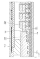

Classifications
-
- G—PHYSICS
- G02—OPTICS
- G02F—OPTICAL DEVICES OR ARRANGEMENTS FOR THE CONTROL OF LIGHT BY MODIFICATION OF THE OPTICAL PROPERTIES OF THE MEDIA OF THE ELEMENTS INVOLVED THEREIN; NON-LINEAR OPTICS; FREQUENCY-CHANGING OF LIGHT; OPTICAL LOGIC ELEMENTS; OPTICAL ANALOGUE/DIGITAL CONVERTERS
- G02F1/00—Devices or arrangements for the control of the intensity, colour, phase, polarisation or direction of light arriving from an independent light source, e.g. switching, gating or modulating; Non-linear optics
- G02F1/01—Devices or arrangements for the control of the intensity, colour, phase, polarisation or direction of light arriving from an independent light source, e.g. switching, gating or modulating; Non-linear optics for the control of the intensity, phase, polarisation or colour
- G02F1/13—Devices or arrangements for the control of the intensity, colour, phase, polarisation or direction of light arriving from an independent light source, e.g. switching, gating or modulating; Non-linear optics for the control of the intensity, phase, polarisation or colour based on liquid crystals, e.g. single liquid crystal display cells
- G02F1/133—Constructional arrangements; Operation of liquid crystal cells; Circuit arrangements
- G02F1/1333—Constructional arrangements; Manufacturing methods
- G02F1/1339—Gaskets; Spacers; Sealing of cells
-
- G—PHYSICS
- G02—OPTICS
- G02F—OPTICAL DEVICES OR ARRANGEMENTS FOR THE CONTROL OF LIGHT BY MODIFICATION OF THE OPTICAL PROPERTIES OF THE MEDIA OF THE ELEMENTS INVOLVED THEREIN; NON-LINEAR OPTICS; FREQUENCY-CHANGING OF LIGHT; OPTICAL LOGIC ELEMENTS; OPTICAL ANALOGUE/DIGITAL CONVERTERS
- G02F1/00—Devices or arrangements for the control of the intensity, colour, phase, polarisation or direction of light arriving from an independent light source, e.g. switching, gating or modulating; Non-linear optics
- G02F1/01—Devices or arrangements for the control of the intensity, colour, phase, polarisation or direction of light arriving from an independent light source, e.g. switching, gating or modulating; Non-linear optics for the control of the intensity, phase, polarisation or colour
- G02F1/13—Devices or arrangements for the control of the intensity, colour, phase, polarisation or direction of light arriving from an independent light source, e.g. switching, gating or modulating; Non-linear optics for the control of the intensity, phase, polarisation or colour based on liquid crystals, e.g. single liquid crystal display cells
- G02F1/133—Constructional arrangements; Operation of liquid crystal cells; Circuit arrangements
- G02F1/1333—Constructional arrangements; Manufacturing methods
- G02F1/133345—Insulating layers
-
- G—PHYSICS
- G02—OPTICS
- G02F—OPTICAL DEVICES OR ARRANGEMENTS FOR THE CONTROL OF LIGHT BY MODIFICATION OF THE OPTICAL PROPERTIES OF THE MEDIA OF THE ELEMENTS INVOLVED THEREIN; NON-LINEAR OPTICS; FREQUENCY-CHANGING OF LIGHT; OPTICAL LOGIC ELEMENTS; OPTICAL ANALOGUE/DIGITAL CONVERTERS
- G02F1/00—Devices or arrangements for the control of the intensity, colour, phase, polarisation or direction of light arriving from an independent light source, e.g. switching, gating or modulating; Non-linear optics
- G02F1/01—Devices or arrangements for the control of the intensity, colour, phase, polarisation or direction of light arriving from an independent light source, e.g. switching, gating or modulating; Non-linear optics for the control of the intensity, phase, polarisation or colour
- G02F1/13—Devices or arrangements for the control of the intensity, colour, phase, polarisation or direction of light arriving from an independent light source, e.g. switching, gating or modulating; Non-linear optics for the control of the intensity, phase, polarisation or colour based on liquid crystals, e.g. single liquid crystal display cells
- G02F1/133—Constructional arrangements; Operation of liquid crystal cells; Circuit arrangements
- G02F1/1333—Constructional arrangements; Manufacturing methods
- G02F1/1335—Structural association of cells with optical devices, e.g. polarisers or reflectors
- G02F1/133509—Filters, e.g. light shielding masks
- G02F1/133512—Light shielding layers, e.g. black matrix
-
- G—PHYSICS
- G02—OPTICS
- G02F—OPTICAL DEVICES OR ARRANGEMENTS FOR THE CONTROL OF LIGHT BY MODIFICATION OF THE OPTICAL PROPERTIES OF THE MEDIA OF THE ELEMENTS INVOLVED THEREIN; NON-LINEAR OPTICS; FREQUENCY-CHANGING OF LIGHT; OPTICAL LOGIC ELEMENTS; OPTICAL ANALOGUE/DIGITAL CONVERTERS
- G02F1/00—Devices or arrangements for the control of the intensity, colour, phase, polarisation or direction of light arriving from an independent light source, e.g. switching, gating or modulating; Non-linear optics
- G02F1/01—Devices or arrangements for the control of the intensity, colour, phase, polarisation or direction of light arriving from an independent light source, e.g. switching, gating or modulating; Non-linear optics for the control of the intensity, phase, polarisation or colour
- G02F1/13—Devices or arrangements for the control of the intensity, colour, phase, polarisation or direction of light arriving from an independent light source, e.g. switching, gating or modulating; Non-linear optics for the control of the intensity, phase, polarisation or colour based on liquid crystals, e.g. single liquid crystal display cells
- G02F1/133—Constructional arrangements; Operation of liquid crystal cells; Circuit arrangements
- G02F1/1333—Constructional arrangements; Manufacturing methods
- G02F1/1343—Electrodes
- G02F1/13439—Electrodes characterised by their electrical, optical, physical properties; materials therefor; method of making
-
- G—PHYSICS
- G02—OPTICS
- G02F—OPTICAL DEVICES OR ARRANGEMENTS FOR THE CONTROL OF LIGHT BY MODIFICATION OF THE OPTICAL PROPERTIES OF THE MEDIA OF THE ELEMENTS INVOLVED THEREIN; NON-LINEAR OPTICS; FREQUENCY-CHANGING OF LIGHT; OPTICAL LOGIC ELEMENTS; OPTICAL ANALOGUE/DIGITAL CONVERTERS
- G02F1/00—Devices or arrangements for the control of the intensity, colour, phase, polarisation or direction of light arriving from an independent light source, e.g. switching, gating or modulating; Non-linear optics
- G02F1/01—Devices or arrangements for the control of the intensity, colour, phase, polarisation or direction of light arriving from an independent light source, e.g. switching, gating or modulating; Non-linear optics for the control of the intensity, phase, polarisation or colour
- G02F1/13—Devices or arrangements for the control of the intensity, colour, phase, polarisation or direction of light arriving from an independent light source, e.g. switching, gating or modulating; Non-linear optics for the control of the intensity, phase, polarisation or colour based on liquid crystals, e.g. single liquid crystal display cells
- G02F1/133—Constructional arrangements; Operation of liquid crystal cells; Circuit arrangements
- G02F1/1333—Constructional arrangements; Manufacturing methods
- G02F1/1343—Electrodes
- G02F1/134309—Electrodes characterised by their geometrical arrangement
- G02F1/134381—Hybrid switching mode, i.e. for applying an electric field with components parallel and orthogonal to the substrates
-
- G—PHYSICS
- G02—OPTICS
- G02F—OPTICAL DEVICES OR ARRANGEMENTS FOR THE CONTROL OF LIGHT BY MODIFICATION OF THE OPTICAL PROPERTIES OF THE MEDIA OF THE ELEMENTS INVOLVED THEREIN; NON-LINEAR OPTICS; FREQUENCY-CHANGING OF LIGHT; OPTICAL LOGIC ELEMENTS; OPTICAL ANALOGUE/DIGITAL CONVERTERS
- G02F2201/00—Constructional arrangements not provided for in groups G02F1/00 - G02F7/00
- G02F2201/50—Protective arrangements
Definitions
- the present invention relates to a display device.
- a liquid crystal panel which is a main component constituting a liquid crystal display device has the following configuration. That is, the liquid crystal panel seals the liquid crystal by sandwiching the liquid crystal between the pair of glass substrates and forming a seal portion around the liquid crystal.
- Both substrates are composed of an array substrate on which TFTs, which are switching elements, pixel electrodes, insulating films, and wirings are formed, and a CF substrate on which color filters and the like are formed.
- TFTs which are switching elements, pixel electrodes, insulating films, and wirings are formed
- CF substrate color filters and the like are formed.
- the seal portion is mainly bonded to the inorganic insulating film. Since the seal portion and the inorganic insulating film have different linear expansion coefficients (coefficients of thermal expansion) of the respective materials, if a temperature change occurs in the usage environment of the liquid crystal panel, the seal portion in the inorganic insulating film is bonded to the bonded portion. When the stress acts and the stress affects the portion of the inorganic insulating film on the display region side and exceeds the adhesiveness of the inorganic insulating film, peeling occurs in the portion on the display region side.
- the transparent electrode film disposed on the upper layer side of the inorganic insulating film has a defect such as a positional shift, which may cause a display defect.
- the stress generated at the bonded portion of the seal portion in the inorganic insulating film is the display region side in the inorganic insulating film. It tends to be affected more easily by this part and display defects tend to occur, and it has been difficult to deal with.
- the present invention has been completed based on the above circumstances, and an object thereof is to suppress the occurrence of display defects.
- the first display device of the present invention is arranged in an opposing manner so as to have an internal space between a first substrate divided into a display region and a non-display region surrounding the display region, and the first substrate.
- the first transparent electrode film disposed in at least the display region in the first substrate, and the seal portion is bonded to the first substrate in a range straddling the display region and the non-display region in the first substrate.
- the internal space is provided between the first substrate and the second substrate facing each other, and the seal portion disposed so as to surround the internal space is interposed.
- the internal space is sealed.
- the first insulating film is arranged in a range straddling the display area and the non-display area on the first substrate, and the seal portion is adhered to the first insulating film, and is sandwiched between the first transparent electrode film and the second transparent electrode film. It is arranged with.
- the thickness of the first insulating film is larger than that in the configuration without the second transparent electrode film. Since the film tends to be relatively thin, peeling is likely to occur in the first insulating film due to the stress acting on the adhesion portion of the seal portion in the first insulating film. In that respect, since the first insulating film has a slit arranged at a position closer to the display area than the seal part in the non-display area, the first insulating film has a slit as described above at the bonding portion of the seal part in the first insulating film.
- the stress Even if the stress is applied, the stress hardly affects the portion of the first insulating film on the display region side. As a result, the display region side portion of the first insulating film is less likely to be peeled off, so that the first transparent electrode film disposed on the upper layer side of the first insulating film in the display region is less likely to be defective. . Therefore, the occurrence of display defects is suppressed, which is particularly suitable for narrowing the frame.
- the second transparent electrode film has an electrode film extended portion that extends and extends to the non-display area, and the first insulating film has a slit formed on the second transparent electrode film. It is provided so as to be disposed at a position overlapping with the electrode film extension.
- the slit for example, when the first insulating film is partially etched using a photolithography method, an electrode of the second transparent electrode film is formed on the first substrate side of the slit forming portion of the first insulating film.
- the electrode film extension portion functions as an etching stopper, and etching can be prevented from reaching the first substrate side of the electrode film extension portion.
- a second insulating film disposed on the first substrate side of the second transparent electrode film and disposed in a range straddling the display area and the non-display area in the first substrate;
- a common potential supply unit disposed in the non-display area of the substrate and disposed on the first substrate side of the second insulating film and configured to have a common potential.
- the common potential supply part is connected through a contact hole formed in the second insulating film.
- the electrode film extension portion is disposed in a range extending between the display area and the non-display area and is second insulated through a contact hole formed in the second insulating film disposed on the first substrate side of the second transparent electrode film.
- the common potential is supplied from the common potential supply unit to the second transparent electrode film having the electrode film extension unit.
- the electrode film extension portion is etched on the first substrate side of the electrode film extension portion when the slit is formed in the first insulating film. Therefore, the configuration can be simplified as compared with a case where another part is provided for each function.
- the first substrate includes a second insulating film disposed in a range straddling the display region and the non-display region and disposed on the first substrate side of the first insulating film,
- the first insulating film is provided so that the slit overlaps with the second insulating film. If it does in this way, the arrangement
- the first insulating film is provided so that the slit penetrates in the film thickness direction of the first insulating film.
- the slit is not penetrated in the film thickness direction of the first insulating film and the thin portion (the portion thinner than the portion where the slit is not formed) is left,
- the stress generated at the bonding portion of the seal portion in one insulating film is less likely to be affected by the portion on the display region side in the first insulating film. Thereby, peeling is less likely to occur in the display area side portion of the first insulating film, and the occurrence of display defects is more preferably suppressed.
- the first insulating film is provided in a portion where the slit is formed so that a thin portion thinner than a portion where the slit is not formed is formed.
- a thin portion is formed at the slit forming portion in the first insulating film.
- the first substrate side of the first insulating film can be avoided from being exposed through the slit, so that the film quality becomes inhomogeneous. Is avoided. This makes it difficult for display performance to deteriorate due to the formation of the slits. Further, the degree of freedom of arrangement of the slits is high.
- the first insulating film is provided so that the slit is disposed closer to the seal portion than the display area.
- the degree of freedom of arrangement of the slit is high, and therefore the slit is arranged closer to the seal portion than the display area. It becomes possible. Even if the stress acts on the adhesion portion of the seal portion in the first insulating film and the separation occurs, the range of the portion that can be peeled off in the first insulating film becomes narrow due to the arrangement of the slits described above. Thereby, even if peeling occurs in the first insulating film, the peeling range is limited, and thus the display performance is hardly adversely affected.
- the first insulating film is provided such that the slit is continuously or intermittently arranged along the entire circumference of the seal portion. According to this configuration, the stress generated at the adhesion portion of the seal portion in the first insulating film due to the slits arranged continuously or intermittently over the entire circumference of the seal portion causes a portion on the display region side in the first insulating film. As a result, it is difficult to cause peeling at the display region side portion of the first insulating film, thereby suppressing display defects.
- the first insulating film is provided so that the slit has a groove shape extending continuously over the entire circumference of the seal portion.
- the stress generated at the bonding portion of the seal portion in the first insulating film is caused by the display area in the first insulating film. It is less affected by the side part. Thereby, peeling is less likely to occur in the display area side portion of the first insulating film, and the occurrence of display defects is more preferably suppressed.
- the first insulating film is provided such that the slit is intermittently disposed over the entire circumference of the seal portion.
- the stress generated at the adhesion portion of the seal portion in the first insulating film due to the slits arranged intermittently over the entire circumference of the seal portion hardly affects the portion on the display region side in the first insulating film. Therefore, peeling does not easily occur in the portion of the first insulating film on the display region side, and the occurrence of display defects is suppressed.
- the second substrate includes a light shielding portion disposed at least in the non-display area, and the first insulating film is provided so that the slit overlaps the light shielding portion.
- the first insulating film is provided so that the slit overlaps with the light shielding portion provided in the second substrate, it is possible to prevent light from passing through the slit forming region in the display device. Thereby, the occurrence of uneven brightness in the transmitted light of the display device is avoided, and the occurrence of display defects is suppressed.
- the second display device of the present invention is arranged in an opposing manner so as to have an internal space between a first substrate divided into a display region and a non-display region surrounding the display region, and the first substrate.
- a first insulating film is used as the first transparent electrode.
- the internal space is provided between the first substrate and the second substrate facing each other, and the seal portion disposed so as to surround the internal space is interposed.
- the internal space is sealed.
- the first insulating film is disposed at least in the display region of the first substrate, and is disposed so as to be sandwiched between the first transparent electrode film and the second transparent electrode film.
- the 1st insulating film is distribute
- the seal portion is directly bonded to the first insulating film, if a stress is generated at the bonding portion of the both in accordance with the temperature change, peeling occurs at a portion of the first insulating film on the display region side. There is a risk that defects such as misalignment may occur in the first transparent electrode film disposed on the upper layer side of the first insulating film.
- the stress generated in the above-mentioned adhesion portion is more likely to be affected by the portion on the display area side in the first insulating film.
- the thickness of the first insulating film is larger than that in the configuration without the second transparent electrode film. Since the film tends to be relatively thin, peeling is likely to occur in the first insulating film due to the stress acting on the adhesion portion of the seal portion in the first insulating film.
- the first insulating film is not directly bonded to the seal portion, a situation in which stress acts on the first insulating film from the seal portion with a temperature change is avoided. As a result, it is possible to avoid peeling of the first insulating film on the display region side, so that a defect such as displacement occurs in the first transparent electrode film disposed on the upper layer side of the first insulating film in the display region. It becomes difficult. Therefore, the occurrence of display defects is suppressed, which is particularly suitable for narrowing the frame.
- the first substrate is disposed at least in the display region and is disposed on the first substrate side of the first insulating film so as to sandwich the first insulating film between the first transparent electrode film and the first transparent electrode film.
- a second insulating film having a thickness larger than that of the first insulating film.
- the thickness of the second insulating film to which the seal portion is bonded is larger than the thickness of the first insulating film. Therefore, even when a stress is applied to the adhesion portion of the seal portion in the second insulating film in accordance with the temperature change, it is difficult for peeling to occur in the display region side portion of the second insulating film.
- the first insulating film having a relatively small film thickness tends to be peeled off due to stress, but the first insulating film is not directly bonded to the seal portion, so that the temperature change is accompanied. The situation where stress acts on the first insulating film from the seal portion is avoided. As a result, it is possible to avoid the occurrence of peeling in the display region side portion of the first insulating film, thereby suppressing the occurrence of display defects.
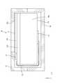
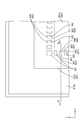
- FIG. 1 is a schematic plan view showing a connection configuration of a liquid crystal panel, a flexible substrate, and a control circuit board on which a driver according to Embodiment 1 of the present invention is mounted.
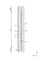
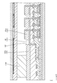
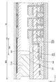
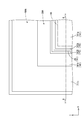
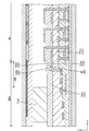
- Schematic cross-sectional view showing a cross-sectional configuration along the long side direction of the liquid crystal display device Schematic cross-sectional view showing the cross-sectional configuration of the entire liquid crystal panel Plan view of array substrate
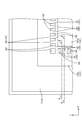
- the top view which shows the wiring structure which connects the shield part, row control circuit part, and column control circuit part which were distribute
- angular part vicinity of the array substrate which concerns on Embodiment 2 of this invention Sectional view taken along line ix-ix in FIG. Xx sectional view of FIG.
- the top view which expanded the corner vicinity of the array substrate which concerns on Embodiment 3 of this invention Sectional view taken along line xii-xii in FIG. Sectional drawing which shows the cross-sectional structure in the edge part of the liquid crystal panel which concerns on Embodiment 4 of this invention.
- angular part vicinity of the array substrate which concerns on Embodiment 5 of this invention Xv-xv sectional view of FIG.
- Sectional drawing which shows the cross-sectional structure in the edge part of the liquid crystal panel which concerns on Embodiment 6 of this invention. Sectional drawing which shows the cross-sectional structure in the edge part of the liquid crystal panel which concerns on Embodiment 7 of this invention.
- the top view which expanded the corner vicinity of the array substrate which concerns on Embodiment 8 of this invention Xix-xix cross-sectional view of FIG.
- the top view which expanded the corner vicinity of the array substrate which concerns on Embodiment 9 of this invention Xxi-xxi sectional view of FIG.
- Sectional drawing which shows the cross-sectional structure in the edge part of the liquid crystal panel which concerns on Embodiment 11 of this invention.
- Sectional drawing which shows the cross-sectional structure in the edge part of the liquid crystal panel which concerns on Embodiment 12 of this invention.
- Sectional drawing which shows the cross-sectional structure in the edge part of the liquid crystal panel which concerns on Embodiment 13 of this invention.
- Sectional drawing which shows the cross-sectional structure in the edge part of the liquid crystal panel which concerns on Embodiment 14 of this invention.
- Sectional drawing which shows the cross-sectional structure in the edge part of the liquid crystal panel which concerns on Embodiment 15 of this invention.
- FIGS. 2, 3 and 7 A first embodiment of the present invention will be described with reference to FIGS.
- the liquid crystal display device 10 is illustrated.
- a part of each drawing shows an X axis, a Y axis, and a Z axis, and each axis direction is drawn to be a direction shown in each drawing.
- FIGS. 2, 3 and 7 are used as a reference, and the upper side of the figure is the front side and the lower side of the figure is the back side.
- the liquid crystal display device 10 is arranged on the outer peripheral side so as to be able to display an image and to surround the display area (active area) AA arranged on the center side and the display area AA.
- a liquid crystal panel (display device, display panel) 11 having a non-display area (non-active area) NAA, a driver (panel driving unit) 21 for driving the liquid crystal panel 11, and various input signals to the driver 21 are supplied from the outside.
- a backlight device (illumination device) 14 as a light source.
- the liquid crystal display device 10 also includes a pair of front and back exterior members 15 and 16 for housing and holding the liquid crystal panel 11 and the backlight device 14 assembled to each other.
- an opening 15a for allowing an image displayed in the display area AA of the liquid crystal panel 11 to be visually recognized from the outside is formed.
- the liquid crystal display device 10 according to the present embodiment includes a mobile phone (including a smartphone), a notebook computer (including a tablet notebook computer), a portable information terminal (including an electronic book, a PDA, etc.), a digital photo frame, It is used for various electronic devices (not shown) such as portable game machines and electronic ink paper. For this reason, the screen size of the liquid crystal panel 11 constituting the liquid crystal display device 10 is set to about several inches to several tens of inches, and is generally classified into a small size and a small size.
- the backlight device 14 includes a chassis 14a having a substantially box shape that opens toward the front side (the liquid crystal panel 11 side), and a light source (not shown) disposed in the chassis 14a (for example, a cold cathode tube, LED, organic EL, etc.) and an optical member (not shown) arranged to cover the opening of the chassis 14a.
- the optical member has a function of converting light emitted from the light source into a planar shape.
- the liquid crystal panel 11 has a vertically long rectangular shape (rectangular shape) as a whole, and is displayed at a position offset toward one end side (the upper side shown in FIG. 1) in the long side direction.
- the area AA is arranged, and the driver 21 and the flexible substrate 13 are respectively attached to positions shifted toward the other end (the lower side shown in FIG. 1) in the long side direction.
- An outer area surrounding the display area AA in the liquid crystal panel 11 is a non-display area NAA in which no image is displayed.
- the non-display area NAA includes a substantially frame-shaped area (a frame portion in a CF substrate 11a described later) surrounding the display area AA, and an area (on an array substrate 11b described later) secured on the other end side in the long side direction.
- the mounting area (mounting area) of the driver 21 and the flexible board 13 is in the area secured on the other end side in the long side direction.
- the short side direction in the liquid crystal panel 11 coincides with the X-axis direction of each drawing, and the long side direction coincides with the Y-axis direction of each drawing.
- a frame-shaped one-dot chain line that is slightly smaller than the CF substrate 11a represents the outer shape of the display area AA, and an area outside the one-dot chain line is a non-display area NAA.
- the control circuit board 12 is attached to the back surface of the chassis 14a (the outer surface opposite to the liquid crystal panel 11 side) of the backlight device 14 with screws or the like.
- the control circuit board 12 is mounted with electronic components for supplying various input signals to the driver 21 on a board made of paper phenol or glass epoxy resin, and wiring (conductive path) of a predetermined pattern (not shown) is provided. Routed formation.
- One end (one end side) of the flexible substrate 13 is electrically and mechanically connected to the control circuit board 12 via an ACF (Anisotropic Conductive Film) (not shown).
- the flexible substrate (FPC substrate) 13 includes a base material made of a synthetic resin material (for example, polyimide resin) having insulating properties and flexibility, and a large number of wirings are provided on the base material. It has a pattern (not shown), and one end in the length direction is connected to the control circuit board 12 arranged on the back side of the chassis 14a as described above, while the other end Since the portion (the other end side) is connected to the array substrate 11 b in the liquid crystal panel 11, the liquid crystal display device 10 is bent in a folded shape so that the cross-sectional shape is substantially U-shaped.
- a synthetic resin material for example, polyimide resin
- the wiring pattern is exposed to the outside to form terminal portions (not shown), and these terminal portions are respectively connected to the control circuit board 12 and the liquid crystal panel 11. Are electrically connected to each other. Thereby, an input signal supplied from the control circuit board 12 side can be transmitted to the liquid crystal panel 11 side.
- the driver 21 is composed of an LSI chip having a drive circuit therein, and operates based on a signal supplied from a control circuit board 12 that is a signal supply source. An input signal supplied from the control circuit board 12 is processed to generate an output signal, and the output signal is output toward the display area AA of the liquid crystal panel 11.
- the driver 21 has a horizontally long rectangular shape when viewed in a plan view (longitudinal along the short side of the liquid crystal panel 11), and also with respect to a non-display area NAA of the liquid crystal panel 11 (array substrate 11b described later). It is mounted directly, that is, COG (Chip On Glass).
- the long side direction of the driver 21 coincides with the X-axis direction (the short side direction of the liquid crystal panel 11), and the short side direction coincides with the Y-axis direction (the long side direction of the liquid crystal panel 11).
- the liquid crystal panel 11 will be described again. As shown in FIG. 3, the liquid crystal panel 11 is sandwiched between a pair of substrates 11a and 11b which are opposed to each other and have an internal space IS therebetween, and is disposed in the internal space IS.
- the liquid crystal layer (liquid crystal) 11c containing liquid crystal molecules, which are substances whose optical characteristics change with application of an electric field, and the substrate 11a, 11b are interposed between the internal space IS and the liquid crystal layer 11c disposed there.
- At least a seal portion 11d that seals the internal space IS and the liquid crystal layer 11c disposed therein is provided.
- the front side is a CF substrate (second substrate, counter substrate) 11a
- the back side is an array substrate (first substrate, TFT substrate, active matrix substrate) 11b.
- the CF substrate 11a and the array substrate 11b are respectively divided into the display area AA and the non-display area NAA described above.
- polarizing plates 11f and 11g are attached to the outer surfaces of both the substrates 11a and 11b, respectively.
- the liquid crystal layer 11c is sealed between the substrates 11a and 11b by a so-called dropping injection method. Specifically, after the liquid crystal material forming the liquid crystal layer 11c is dropped on the CF substrate 11a, the array is formed on the CF substrate 11a. When the substrate 11b is bonded, the liquid crystal material is uniformly spread in the internal space IS formed between the substrates 11a and 11b. As shown in FIGS. 1 and 3, the seal portion 11d is arranged in the non-display area NAA of the liquid crystal panel 11 and is viewed in a plan view (viewed from the normal direction with respect to the plate surfaces of the substrates 11a and 11b). It has a vertically long substantially frame shape following the non-display area NAA (FIGS. 1 and 4).
- the seal portion 11d is formed on the CF substrate 11a of the pair of substrates 11a and 11b in the manufacturing process of the liquid crystal panel 11.
- the width dimension of the seal portion 11d is smaller than the narrowest width dimension in the non-display area NAA (specifically, the width dimension in three side portions excluding the side portion on the driver 21 side).
- the inner end position of the seal portion 11d is arranged outside the boundary position between the display area AA and the non-display area NAA (on the opposite side to the display area AA side).
- a seal portion non-arrangement region SNA having a frame shape (frame shape) in a plan view following the seal portion 11d is present on the inner side (display region AA side) of the seal portion 11d in the non-display region NAA.
- the width dimension is equal to the distance between the inner end position of the seal portion 11d and the boundary position between the display area AA and the non-display area NAA.
- the seal portion 11d includes an ultraviolet curable resin material (curable resin material) that is cured by being irradiated with ultraviolet rays.
- the ultraviolet curable resin material contained in the seal portion 11d is in a liquid state having fluidity before being irradiated with ultraviolet rays, the ultraviolet curable resin material is cured into a solid state when irradiated with ultraviolet rays. Yes.
- the portion of the seal portion 11d that is disposed at the end portions (non-mounting side end portions) of the remaining three sides excluding the mounting area of the driver 21 and the flexible substrate 13 in the liquid crystal panel 11 is in the non-display area NAA. It is arranged at the outermost end position (FIG. 1).
- Each of the CF substrate 11a and the array substrate 11b includes a substantially transparent (highly translucent) glass substrate (substrate) GS, and various films (structures) are laminated on the glass substrate GS. It is supposed to be.
- the CF substrate 11a has a short side dimension substantially equal to that of the array substrate 11b as shown in FIGS. 1 and 2, but the long side dimension is smaller than that of the array substrate 11b. It is bonded to 11b with one end (upper side shown in FIG. 1) in the long side direction aligned. Therefore, the other end (the lower side shown in FIG.
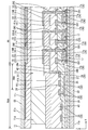
- FIG. 7 schematically shows a film (structure) provided on each of the substrates 11a and 11b, and the size (thickness, height, etc.) and arrangement of each illustrated structure are not necessarily actual. It is not consistent with the size or arrangement of
- the operation mode is an FFS (Fringe Field Switching) mode in which the IPS (In-Plane Switching) mode is further improved.
- FFS Flexible Field Switching
- IPS In-Plane Switching
- substrate 11a, 11b is equipped is demonstrated in detail.
- the CF substrate 11a includes a light shielding portion (black matrix) 11i, a color filter 11h, a CF substrate side planarizing film (overcoat film) 11j, in order from the lower layer (glass substrate GS, front side).
- a solid pattern arranged on the liquid crystal layer 11c is formed on the upper side of the CF substrate side planarizing film 11j, and the liquid crystal molecules contained in the liquid crystal layer 11c are arranged.
- An alignment film for alignment is laminated, for example, made of polyimide.
- a columnar photo spacer portion is provided on the upper side of the CF substrate side planarizing film 11j so as to protrude through the liquid crystal layer 11c toward the array substrate 11b side.
- the cell gap can be kept constant mainly in the display area AA.
- the light shielding portion 11i is arranged on the surface of the glass substrate GS forming the CF substrate 11a so as to straddle the display area AA and the non-display area NAA.
- carbon black is included to provide high light shielding properties.
- the light-shielding portion 11i is patterned in a lattice pattern when viewed from the plane, while the portion disposed in the display area AA is framed when viewed from the same plane as the seal portion 11d. It is patterned in a shape (frame shape).
- the color filter 11h is arranged in the display area AA, and is patterned in an island shape according to the arrangement of pixel electrodes 18 on the array substrate 11b side described later.
- the photosensitive resin material contains a pigment for coloring.
- the color filter 11h includes a large number of coloring portions arranged in a matrix (matrix shape) in positions that overlap each pixel electrode 18 on the array substrate 11b side in a plane in the display area AA of the CF substrate 11a. 11hR, 11hG, and 11hB. Each of the colored portions 11hR, 11hG, and 11hB has a vertically long rectangular shape when viewed in a plane (not shown).
- the color filter 11h configures a colored portion group by alternately arranging the colored portions 11hR, 11hG, and 11hB, each of red, green, and blue, along the row direction (X-axis direction).
- the adjacent colored portions 11hR, 11hG, and 11hB in the display area AA are partitioned by a grid-like portion in the light shielding portion 11i, thereby preventing color mixture between pixels.
- Both the light shielding portion 11i and the color filter 11h are formed by patterning on the CF substrate 11a by a known photolithography method in the manufacturing process.
- the CF substrate side planarizing film 11j is laminated on the upper side of the light shielding portion 11i and the color filter 11h, and has a solid pattern extending over the display area AA and the non-display area NAA. It is made of an acrylic resin material such as acid methyl resin (PMMA).
- the CF substrate side planarizing film 11j has a film thickness larger than that of the color filter 11h and the light shielding portion 11i, so that the surface on the liquid crystal layer 11c side (the surface on which the alignment film is disposed) in the CF substrate 11a is preferably used. It is flattened. Further, among the CF substrate side planarizing film 11j disposed on the upper layer side than the color filter 11h and the light shielding portion 11i, a portion disposed in the non-display area NAA overlaps with the seal portion 11d in a plan view. The seal part 11d is bonded.
- the upper layer side of the first interlayer insulating film 41 and the first transparent electrode film 23 has a solid pattern arranged facing the liquid crystal layer 11c and the liquid crystal layer 11c.
- An alignment film for aligning the liquid crystal molecules contained in is laminated, and is made of, for example, polyimide.
- the base coat film 37 is a solid pattern covering the entire surface of the glass substrate GS forming the array substrate 11b, and is made of, for example, silicon oxide (SiO 2), silicon nitride (SiNx), silicon nitride oxide (SiNO), or the like. .
- the semiconductor film 36 is stacked on the upper layer side of the base coat film 37 and is patterned into an island shape at least in the display area AA in accordance with the arrangement of TFTs 17 to be described later.
- the semiconductor film 36 is made of a CG silicon (Continuous Grain Silicon) thin film which is a kind of polycrystalline silicon thin film (polycrystalline silicon thin film).
- the CG silicon thin film is formed, for example, by adding a metal material to an amorphous silicon thin film and performing a heat treatment for a short time at a low temperature of about 550 ° C. or less, thereby making the atomic arrangement in the crystal grain boundary of the silicon crystal continuous.
- the gate insulating film 35 is stacked on the upper side of the base coat film 37 and the semiconductor film 36 and has a solid pattern extending over the display area AA and the non-display area NAA.
- silicon oxide (SiO 2) It is supposed to consist of
- the second metal film 34 is laminated on the upper layer side of the gate insulating film 35 and is patterned so as to be disposed in the display area AA and the non-display area NAA, for example, titanium (Ti) and copper (Cu).
- the laminated film is formed.
- the second interlayer insulating film 39 is stacked on the upper side of the gate insulating film 35 and the second metal film 34, and has a solid pattern extending over the display area AA and the non-display area NAA. It is made of silicon oxide (SiO2).
- the first metal film 38 is laminated on the upper layer side of the second interlayer insulating film 39 and is patterned so as to be respectively disposed in the display area AA and the non-display area NAA.
- the passivation film is laminated on the upper layer of the first metal film 38 and has a solid pattern extending over the display area AA and the non-display area NAA.
- the passivation film is made of silicon oxide (SiO 2). This passivation film is necessary when the first metal film 38 is used outside the cell (outside the seal) in order to reduce the wiring load.
- the planarizing film 40 is laminated on the upper side of the second interlayer insulating film 39 and the first metal film 38, and has a solid pattern extending over the display area AA and the non-display area NAA. It is made of an acrylic resin material such as polymethyl methacrylate resin (PMMA).
- the film thickness of the planarizing film 40 is preferably in the range of 2 ⁇ m to 3 ⁇ m, and in this embodiment is about 2.5 ⁇ m.
- the second transparent electrode film 24 is laminated on the upper side of the flattening film 40 and has a substantially solid pattern extending over the display area AA and the non-display area NAA.
- ITO Indium Tin Oxide
- ZnO Zinc
- the first interlayer insulating film 41 is laminated on the upper side of the planarizing film 40 and the second transparent electrode film 24, and has a solid pattern extending over the display area AA and the non-display area NAA.
- it is made of silicon nitride (SiNx).
- the thickness of the first interlayer insulating film 41 is preferably in the range of 0.05 ⁇ m to 1 ⁇ m, and in particular, the range of 0.05 ⁇ m to 0.2 ⁇ m is to ensure insulation reliability, manufacturing cost, Further, it is more preferable from the viewpoint of the tact time for manufacturing, and in this embodiment, it is about 0.1 ⁇ m.
- the second transparent electrode film 24 is disposed so as to be sandwiched between the planarization film 40 on the lower layer side and the first interlayer insulating film 41 on the upper layer side.
- the first transparent electrode film 23 is laminated on the upper layer side of the first interlayer insulating film 41, and is patterned in an island shape in accordance with the arrangement of the TFT 17 in the display area AA.
- ITO Indium Tin Oxide
- ZnO It is made of a transparent electrode material such as (Zinc Oxide).
- the planarizing film 40 which is an organic insulating film, has a film thickness as shown in FIG. It is relatively large compared to the other insulating films 35, 39, and 41 that are inorganic insulating films. Therefore, the planarizing film 40 can suitably planarize the surface of the array substrate 11b on the liquid crystal layer 11c side (the surface on which the alignment film is disposed), and compared with the other insulating films 35, 39, and 41. Peeling is less likely to occur when stress is applied.
- the first interlayer insulating film 41 disposed on the uppermost layer side is disposed in the non-display area NAA.
- the portion to be overlapped with the seal portion 11d in a plan view and the seal portion 11d is bonded.
- the gate insulating film 35, the second interlayer insulating film 39, the planarizing film 40, and the first interlayer insulating film 41 are patterned in the manufacturing process of the array substrate 11b, so that contact holes are formed at respective predetermined positions. Openings such as CH1 to CH3 are formed.
- a large number of TFTs (thin film transistors, display elements) 17 and pixel electrodes 18 which are switching elements are provided side by side in a matrix.
- a gate wiring (scanning signal line, row control line) 19 and a source wiring (column control line, data line) 20 having a lattice shape are disposed so as to surround the electrode 18.
- the TFT 17 and the pixel electrode 18 are arranged in parallel in a matrix at the intersection of the gate wiring 19 and the source wiring 20 that form a lattice.
- the gate wiring 19 is made of the second metal film 34, whereas the source wiring 20 is made of the first metal film 38, and the second interlayer insulating film 39 is disposed between the intersecting portions. Yes. As will be described in detail below, the gate wiring 19 and the source wiring 20 are connected to the gate electrode 17a and the source electrode 17b of the TFT 17, respectively, and the pixel electrode 18 is connected to the drain electrode 17c of the TFT 17.
- the gate electrode 17a is made of the same second metal film 34 as the gate wiring 19, whereas the source electrode 17b and the drain electrode 17c are made of the same first metal film 38 as the source wiring 20 (see FIG. 7).
- an auxiliary capacitance line (not shown) is provided in parallel with the gate line 19 and overlapping a part of the pixel electrode 18 in a plan view.
- This auxiliary capacitance line is made of the same second metal film 34 as the gate line 19.
- the TFT 17 disposed in the display area AA is disposed in a channel portion 17 d made of the semiconductor film 36, and in a form overlapping with the channel portion 17 d on the upper layer side via the gate insulating film 35.
- a gate electrode 17a and a source electrode 17b and a drain electrode 17c arranged on the upper layer side with respect to the gate electrode 17a via the second interlayer insulating film 39 are provided, and a so-called top gate type (stagger type) is provided. ing.
- the source electrode 17b and the drain electrode 17c are connected to the channel portion 17d through contact holes CH1 formed in the gate insulating film 35 and the second interlayer insulating film 39, respectively.
- Electrons can move between the drain electrode 17c.
- the semiconductor film 36 constituting the channel portion 17d is made of a CG silicon thin film as described above. Since this CG silicon thin film has an electron mobility as high as about 200 to 300 cm 2 / Vs, for example, compared to an amorphous silicon thin film or the like, the semiconductor film 36 made of this CG silicon thin film is used as the channel portion 17 d of the TFT 17. Thus, the TFT 17 can be miniaturized to maximize the amount of light transmitted through the pixel electrode 18, which is suitable for achieving high definition and low power consumption.
- the pixel electrode 18 made of the first transparent electrode film 23 is connected to the drain electrode 17c of the TFT 17 through contact holes CH2 formed in the planarization film 40 and the first interlayer insulating film 41, respectively.
- a current flows between the source electrode 17b and the drain electrode 17c via the channel portion 17d, and a predetermined potential is applied to the pixel electrode 18.
- the pixel electrode 18 has a vertically long shape in plan view following the outer shape of the colored portions 11hR, 11hG, and 11hB that form the color filter 11h facing each other, and the opposed colored portions 11hR, 11hG, A pixel (unit pixel) is formed together with 11hB.
- the common electrode 22 made of the second transparent electrode film 24 is arranged so as to overlap the pixel electrode 18 in plan view with the first interlayer insulating film 41 interposed therebetween. Since a common potential (reference potential) is supplied to the common electrode 22 from a common potential supply unit 29 described later, the potential applied to the pixel electrode 18 by the TFT 17 is controlled as described above, whereby both electrodes A predetermined potential difference can be generated between 18 and 22.
- the liquid crystal layer 11c has a fringe electric field (diagonal electric field) including a component in the normal direction to the plate surface of the array substrate 11b in addition to the component along the plate surface of the array substrate 11b.
- the alignment state of the liquid crystal molecules contained in the liquid crystal layer 11c can be appropriately switched.
- the pixel electrode 18 is located at a position overlapping the contact hole CH2 of the planarization film 40 and the first interlayer insulating film 41 in a plan view. An opening for passing the contact portion is formed.
- a column control circuit unit 27 is provided at a position adjacent to the short side of the display area AA in the non-display area NAA of the array substrate 11b, as shown in FIG.
- a row control circuit portion (circuit portion) 28 is provided at a position adjacent to the long side portion in the display area AA.
- the column control circuit unit 27 is connected to the source wiring 20, and the row control circuit unit 28 is connected to the gate wiring 19, so that control for supplying an output signal from the driver 21 to the TFT 17 can be performed. Has been.
- the column control circuit unit 27 and the row control circuit unit 28 are each monolithically formed on the array substrate 11b based on the same semiconductor film 36 as the TFT 17, and thereby control for controlling supply of output signals to the TFT 17 is performed. It has a circuit and its circuit elements.
- the circuit elements constituting the control circuit include, for example, a circuit TFT (circuit thin film transistor) (not shown) using the semiconductor film 36 as a channel portion.
- the control circuit includes a circuit first wiring portion 25 made of the second metal film 34, a circuit second wiring portion 26 made of the first metal film 38, and the like.
- the column control circuit unit 27 and the row control circuit unit 28 are arranged in a range extending over the inner part of the sheet part 11d and the outer part of the seal part non-arrangement area SNA in the non-display area NAA.
- the column control circuit unit 27 has a switch circuit (RGB switch circuit) that distributes the image signal included in the output signal from the driver 21 to each source wiring 20 corresponding to each color pixel of R, G, B. is doing.
- the column control circuit unit 27 can include an attached circuit such as a level shifter circuit or an ESD protection circuit.
- the row control circuit unit 28 has a scanning circuit that supplies a scanning signal included in an output signal from the driver 21 to each gate wiring 19 at a predetermined timing and sequentially scans each gate wiring 19. ing. Further, the row control circuit unit 28 can be provided with an attached circuit such as a level shifter circuit or an ESD protection circuit.
- the column control circuit unit 27 and the row control circuit unit 28 are connected to the driver 21 by connection wiring (not shown) formed on the array substrate 11b.
- a common potential supply unit 29 for supplying a common potential to the common electrode 22 is provided in the non-display area NAA of the array substrate 11b.
- the common potential supply unit 29 is made of the first metal film 38 and is arranged in the non-display area NAA at the inner portion of the seal part non-arrangement area SNA, in other words, between the row control circuit section 28 and the display area AA. ing.
- the second transparent electrode film 24 that forms the common electrode 22 has an electrode film extension 24a that extends to the non-display area NAA, and an end of the electrode film extension 24a is a common potential supply unit.
- the non-display area NAA is provided with a shield portion 30 for shielding the internal space IS of the liquid crystal panel 11.
- the shield part 30 is made of the second metal film 34, and is arranged so as to overlap with the outer part of the sheet part 11d in a non-display area NAA in a plan view, and has a frame shape in a plan view following the seal part 11d. There is no.
- the column control circuit unit 27, the row control circuit unit 28, the common potential supply unit 29, and the shield unit 30 described above are simultaneously performed by a known photolithography method when patterning various films in the manufacturing process of the array substrate 11b. Patterned on the array substrate 11b.
- the seal part 30 is configured by the second metal film 34 is illustrated, but the entire or part of the shield part 30 may be configured by the first metal film 38.
- the shield part 30 on the outer peripheral side is provided by the second metal film 34
- the shield part 30 on the inner peripheral side is provided by the first metal film 38.
- Each is preferably configured.
- the seal portion 11d is bonded to the first interlayer insulating film 41 in the array substrate 11b, and the linear expansion coefficient (thermal expansion) of the material forming each of the seal portion 11d and the first interlayer insulating film 41 is used. Rate) is different. For this reason, when a temperature change occurs in the usage environment of the liquid crystal panel 11, a stress acts on the adhesion portion of the seal portion 11 d in the first interlayer insulating film 41, and the stress is on the display area AA side in the first interlayer insulating film 41. When the portion is affected, there is a possibility that peeling occurs in the portion on the display area AA side in the first interlayer insulating film 41.
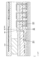
- the slit 42 arranged at the position closer to the display area AA than the seal portion 11 d in the non-display area NAA. Is provided.
- the display area AA is displaced from the first transparent electrode film 23 disposed on the upper layer side of the first interlayer insulating film 41. Defects such as are difficult to occur. Therefore, the occurrence of display defects is suppressed, which is particularly suitable for narrowing the frame.
- the configuration of the slit 42 will be described in detail.
- the slit 42 is arranged in the non-display area NAA of the array substrate 11 b at a position closer to the display area AA than the seal part 11 d, that is, in the seal part non-arrangement area SNA. Is arranged at the inner end position adjacent to the display area AA in the seal part non-arrangement area SNA.
- the slits 42 are arranged at positions adjacent to the outer peripheral side with respect to the display area AA (positions closest to the display area AA) in the seal portion non-arrangement area SNA.
- the slit 42 is formed in a groove shape continuously extending over the entire circumference following the seal portion 11d, and has a frame shape (frame shape) when seen in a plan view. That is, the slit 42 is arranged so as to surround the display area AA from the outer peripheral side over the entire circumference.
- the slit 42 is configured to penetrate the first interlayer insulating film 41 in the film thickness direction (Z-axis direction, normal direction of the plate surface of the array substrate 11b). Accordingly, the first interlayer insulating film 41 is separated into an inner peripheral side portion 41a mainly disposed in the display area AA and an outer peripheral side portion 41b mainly disposed in the non-display area NAA with the slit 42 as a boundary ( Divided).
- the seal portion 11d is bonded to the outer peripheral side portion 41b. Therefore, even when the stress generated with the temperature change acts on the outer peripheral side portion 41b having the adhesion portion of the seal portion 11d in the first interlayer insulating film 41, the inner peripheral side portion 41a separated by the slit 42. Furthermore, the transmission of the stress described above is cut off. As a result, a situation in which peeling occurs in the inner peripheral side portion 41a disposed in the display area AA in the first interlayer insulating film 41 is more reliably avoided, and thus the occurrence of display defects is more reliably prevented.
- the slit 42 is formed by patterning the first interlayer insulating film 41 by a known photolithography method in the manufacturing process of the array substrate 11b, and is formed simultaneously with the contact hole CH2 (in the same process). Has been.
- the slit 42 is arranged at a position overlapping the electrode film extended portion 24 a of the second transparent electrode film 24 in a non-display area NAA when viewed in a plane.
- the lower electrode film extension 24a faces the liquid crystal layer 11c through the slit 42 (exposure). It is configured to be distributed. Accordingly, when the slits 42 are formed in the first interlayer insulating film 41 by photolithography, the portions of the first interlayer insulating film 41 where the slits 42 are to be formed are etched.
- the electrode film extension 24a of the second transparent electrode film 24 By arranging the electrode film extension 24a of the second transparent electrode film 24 on the lower layer side, the electrode film extension 24a functions as an etching stopper, and etching is performed on the planarizing film 40 on the lower layer side of the electrode film extension 24a. It is avoided that it reaches up to. Thereby, the film thickness uniformity of the planarizing film 40 is kept good.
- the electrode film expansion portion 24 a is used when the slit 42 is formed in the first interlayer insulating film 41 in addition to the function of transmitting the common potential from the common potential supply portion 29 to the second transparent electrode film 24.
- the configuration can be simplified as compared with the case where another part is provided for each function. Yes.
- the slit 42 is arranged at a position overlapping with the portion arranged in the non-display area NAA in the light shielding part 11i provided in the CF substrate 11a when viewed in plan.
- the slit 42 is arranged so as to overlap the light shielding portion 11i as described above. This prevents light from being transmitted through the formation region of the slit 42. Thereby, it is possible to avoid luminance unevenness in the transmitted light of the liquid crystal panel 11, and to suppress the occurrence of display defects.
- the liquid crystal panel (display device) 11 of the present embodiment includes the array substrate (first substrate) 11b divided into the display area AA and the non-display area NAA surrounding the display area AA, the array substrate 11b, A CF substrate (second substrate) 11a disposed in an opposing manner with an internal space IS between the array substrate 11b and the CF substrate 11a, and a non-display area surrounding the internal space IS
- a seal portion 11d which is disposed on the NAA and seals the internal space IS
- a first transparent electrode film 23 disposed on at least the display area AA in the array substrate 11b, and a display area AA and a non-display area NAA in the array substrate 11b
- a first interlayer insulating film (first insulating film) disposed on the array substrate 11b side of the first transparent electrode film 23 while the seal portion 11d is adhered in a range extending over 1 and a first interlayer insulating film 41 having a slit 42 disposed at a position closer to the display area AA
- the internal space IS is provided and the seal portion 11d disposed so as to surround the internal space IS is interposed.
- the internal space IS is sealed by the seal portion 11d.
- the first interlayer insulating film 41 is arranged in a range straddling the display area AA and the non-display area NAA in the array substrate 11b, and the seal portion 11d is adhered thereto.
- the first transparent electrode film 23 and the second transparent electrode film 24 It is arranged in the form of being sandwiched between.
- the first interlayer insulating film 41 is compared with the configuration in which the second transparent electrode film 24 is not provided. Since the film thickness of the insulating film 41 tends to be relatively thin, the first interlayer insulating film 41 is likely to be peeled off by the stress acting on the adhesion portion of the seal portion 11 d in the first interlayer insulating film 41. In that respect, since the first interlayer insulating film 41 has the slits 42 arranged at the position closer to the display area AA than the seal part 11d in the non-display area NAA, the seal part in the first interlayer insulating film 41 is provided.
- the stress as described above acts on the adhesion portion 11d, the stress hardly affects the portion of the first interlayer insulating film 41 on the display area AA side. This makes it difficult for the first interlayer insulating film 41 to be peeled off at the display area AA side. Therefore, the display area AA is displaced from the first transparent electrode film 23 disposed on the upper layer side of the first interlayer insulating film 41. Defects such as are difficult to occur. Therefore, the occurrence of display defects is suppressed, which is particularly suitable for narrowing the frame.
- the second transparent electrode film 24 has an electrode film extended portion 24 a that is extended to the non-display area NAA, and the first interlayer insulating film 41 has the slit 42 in the second transparent electrode film 24.
- the electrode film extended portion 24a is provided so as to overlap with the electrode film extended portion 24a.
- the electrode film extension 24a of the transparent electrode film 24 the electrode film extension 24a functions as an etching stopper, and etching can be prevented from reaching the array substrate 11b side of the electrode film extension 24a.
- a planarizing film (second insulating film) 40 disposed on the array substrate 11b side of the second transparent electrode film 24 and disposed in a range straddling the display area AA and the non-display area NAA in the array substrate 11b,
- the array substrate 11b includes a common potential supply unit 29 that is disposed in the non-display area NAA and is disposed on the array substrate 11b side of the planarization film 40 and is set to a common potential.
- the common potential supply unit 29 is connected through a contact hole CH3 formed in the planarizing film 40.
- the electrode film extension 24a is arranged in a range extending over the display area AA and the non-display area NAA, and is a contact hole formed in the planarizing film 40 which is arranged on the array substrate 11b side of the second transparent electrode film 24. Since it is connected to the common potential supply unit 29 disposed on the array substrate 11b side of the planarization film 40 through CH3, the common potential is applied from the common potential supply unit 29 to the second transparent electrode film 24 having the electrode film extension unit 24a. Supplied.
- the electrode film expansion portion 24a has the function of transmitting the common potential to the second transparent electrode film 24, and when the slit 42 is formed in the first interlayer insulating film 41, the array substrate of the electrode film expansion portion 24a. Since it has a function of preventing the 11b side from being etched, the configuration can be simplified as compared with a case where another part is provided for each function.
- the first interlayer insulating film 41 is provided so that the slit 42 penetrates in the film thickness direction of the first interlayer insulating film 41.
- the slit is not penetrated in the film thickness direction of the first interlayer insulating film 41 and the thin portion (the portion thinner than the portion where the slit is not formed) is left.
- the stress generated at the bonding portion of the seal portion 11d in the first interlayer insulating film 41 is less affected by the portion on the display area AA side in the first interlayer insulating film 41. As a result, peeling is less likely to occur in the portion of the first interlayer insulating film 41 on the display area AA side, and the occurrence of display defects is more suitably suppressed.
- the first interlayer insulating film 41 is provided so that the slit 42 has a groove shape extending continuously over the entire circumference of the seal portion 11d. In this way, the stress generated in the bonding portion of the seal portion 11d in the first interlayer insulating film 41 due to the slits 42 continuously arranged over the entire circumference of the seal portion 11d is displayed on the first interlayer insulating film 41. Since it is difficult to affect the portion on the area AA side, peeling does not easily occur in the portion on the display area AA side in the first interlayer insulating film 41, and the occurrence of display defects is suppressed.
- the stress generated at the bonding portion of the seal portion 11d in the first interlayer insulating film 41 is caused by the stress generated in the first interlayer insulating film 41. Is less affected by the portion on the display area AA side. As a result, peeling is less likely to occur in the portion of the first interlayer insulating film 41 on the display area AA side, and the occurrence of display defects is more suitably suppressed.
- the CF substrate 11a includes a light shielding portion 11i disposed at least in the non-display area NAA, and the first interlayer insulating film 41 is provided so that the slit 42 overlaps the light shielding portion 11i.
- the first interlayer insulating film 41 is provided so that the slit 42 overlaps with the light shielding portion 11 i provided in the CF substrate 11 a, the light is transmitted through the formation region of the slit 42 in the liquid crystal panel 11. Is avoided. Thereby, the occurrence of uneven brightness in the transmitted light of the liquid crystal panel 11 is avoided, and the occurrence of display defects is suppressed.
- Embodiment 2 A second embodiment of the present invention will be described with reference to FIGS. In this Embodiment 2, what changed the planar shape of the slit 142 is shown. In addition, the overlapping description about the same structure, operation
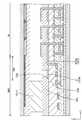
- the slits 142 are intermittently arranged along the entire circumference of the seal portion 111d as shown in FIGS. Specifically, the slits 142 are arranged in a plurality of rows with a predetermined interval in the circumferential direction so as to form a frame shape when seen in a plan view like the seal portion 111d as a whole. Each of the plurality of slits 142 arranged in a frame shape as a whole has a rectangular shape when seen in a plan view. The parts are arranged in an intervening manner. A portion of the first interlayer insulating film 141 that remains between the adjacent slits 142 is the inter-slit remaining portion 43.
- the inter-slit remaining portion 43 is intermittently arranged along the entire circumference following the seal portion 111d, and connects the inner peripheral portion 141a and the outer peripheral portion 141b in the first interlayer insulating film 141. . That is, the inner peripheral side portion 141a and the outer peripheral side portion 141b in the first interlayer insulating film 141 are not connected to each other over the entire periphery, and are mutually connected by the plurality of remaining portions 43 between the slits arranged in an intermittent manner. Are partially connected in the circumferential direction.
- the stress acting on the outer peripheral portion 141b is obtained by adding the width of the inter-slit remaining portion 43 and the width of the slit 142 to the width of the inter-slit remaining portion 43 until reaching the inner peripheral portion 141a. It is attenuated by the ratio obtained by dividing by the numerical value, and it is assumed that the inner peripheral side portion 141a is hardly peeled off.
- the first interlayer insulating film 141 is provided such that the slits 142 are intermittently arranged over the entire circumference of the seal portion 111d.
- the stress generated at the bonding location of the seal portion 111d in the first interlayer insulating film 141 by the slits 142 intermittently arranged over the entire circumference of the seal portion 111d causes the display region in the first interlayer insulating film 141 to be displayed. Since it is difficult to affect the portion on the AA side, peeling does not easily occur in the portion on the display area AA side in the first interlayer insulating film 141, and the occurrence of display defects is suppressed.
- Embodiment 3 A third embodiment of the present invention will be described with reference to FIG. 11 or FIG. In this Embodiment 3, what changed further the planar shape of the slit 242 from above-mentioned Embodiment 2 is shown. In addition, the overlapping description about the same structure, an effect
- the slits 242 are arranged so as to form a frame shape in a plan view following the seal portion 211d as a whole, and in addition to the circumferential direction, the width direction Are also arranged side by side at predetermined intervals. That is, the slits 242 have a frame shape as a whole, but are arranged in a plane so that a plurality of slits 242 are intermittently arranged in a matrix.
- the interval between the slits 242 adjacent to each other in the circumferential direction and the width direction described above is narrower than the interval between the slits 142 described in the second embodiment.
- the inter-slit remaining portion 243 is disposed, and the width dimension of each inter-slit remaining portion 243 is the same as that of the above-described second embodiment. It is smaller than the width dimension of the described inter-slit remaining portion 43.
- the slit-to-slit remaining portions 243 are arranged in a plane in such a manner that a plurality of them are intermittently arranged in a matrix, and those adjacent in the circumferential direction are connected to each other and adjacent in the width direction. By connecting the objects to each other, the whole is formed in a lattice shape in a plan view.
- the stress acting on the outer peripheral portion 241b is obtained by adding the width of the remaining portion 243 between the slits and the width of the remaining portion 243 between the slits 242 before reaching the inner peripheral portion 241a. It is attenuated by the ratio obtained by dividing by the numerical value, and it is assumed that the inner peripheral side portion 241a hardly peels off.
- Embodiment 4 A fourth embodiment of the present invention will be described with reference to FIG. In this Embodiment 4, what changed the depth of the slit 342 from above-mentioned Embodiment 1 is shown. In addition, the overlapping description about the same structure, operation
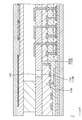
- the slit 342 is formed with a depth that does not penetrate the first interlayer insulating film 341 in the film thickness direction. That is, the depth dimension of the slit 342 is less than the thickness of the first interlayer insulating film 341. Therefore, a thin portion 44 is formed in the first interlayer insulating film 341 where the slit 342 is formed, which is thinner than the thickness of the first interlayer insulating film 341 where the slit 342 is not formed.
- the portion where the film thickness is relatively larger than that of the thin portion 44 is not formed in the portion where the slit 342 is formed, the portion overlapping the seal portion 311d in the outer peripheral portion 341b in a plan view, An inner peripheral portion 341a is included.
- the slit 342 and the thin-walled portion 44 are arranged so as to continuously extend over the entire circumference following the seal portion 311d. Therefore, the thin portion 44 connects the inner peripheral side portion 341a and the outer peripheral side portion 341b in the first interlayer insulating film 341 over the entire periphery.
- a photomask used for exposing the first interlayer insulating film 341 in an exposure process in the manufacturing process of the array substrate 311b is used as a halftone mask or a graytone mask (not shown). Yes. Since the halftone mask or the gray tone mask has a semi-transmissive region in which the transmittance of exposure light is about 10% to 70%, for example, in the exposure process, The portions where the slits 342 and the thin portion 44 are to be formed in the first interlayer insulating film 341 are exposed. By performing an exposure process after performing an exposure process using such a half-tone mask or a gray-tone mask, the slit 342 can be formed with the thin portion 44 remaining.
- the thin portion 44 is left in the portion where the slit 342 is formed, so that the etching does not reach the lower layer side of the first interlayer insulating film 341.
- the electrode film extended portion 324a of the second transparent electrode film 324 is disposed on the lower layer side of the thin portion 44, the slit 342 is formed with a depth that penetrates the first interlayer insulating film 341 by etching. Even in such a case, the electrode film extended portion 324a functions as an etching stopper, so that a situation in which the lower planarizing film 340 is etched is avoided. Thereby, the film thickness uniformity of the planarization film 340 can be maintained high.
- the electrode film extended portion 324a disposed on the lower layer side of the first interlayer insulating film 341 is covered with the thin portion 44 and is not exposed to the liquid crystal layer 311c side, the electrode film extended portion 324a faces the liquid crystal layer 311c. Inhomogeneous film quality on the surface is avoided. This makes it difficult for display performance to deteriorate due to the formation of the slits 342. Further, for example, even if the slit 342 is disposed so as not to overlap with the electrode film extended portion 324a, the lower portion of the planarizing film 340 can be prevented from being etched by the thin portion 44. The degree of freedom is high.
- the first interlayer insulating film 341 is provided so that the thinner portion 44 is formed in the portion where the slit 342 is formed than in the portion where the slit 342 is not formed.
- the slit 342 is formed, for example, when the first interlayer insulating film 341 is partially etched by using a photolithography method, the thin-walled portion 44 is left in the portion where the slit 342 is formed in the first interlayer insulating film 341.
- the etching can be prevented from reaching the array substrate 311b side of the first interlayer insulating film 341.
- the slit is formed so as to penetrate the first interlayer insulating film 341 in the film thickness direction, it is avoided that the array substrate 311b side of the first interlayer insulating film 341 is exposed through the slit 342. Is prevented from becoming heterogeneous. This makes it difficult for display performance to deteriorate due to the formation of the slits 342. Moreover, the arrangement
- a fifth embodiment of the present invention will be described with reference to FIG.
- the fifth embodiment shows a configuration in which the slit is omitted from the first embodiment and the outer peripheral side portion of the first interlayer insulating film 441 is removed.
- movement, and effect as above-mentioned Embodiment 1 is abbreviate
- the first interlayer insulating film 441 is configured only by the inner peripheral side portion 441 a disposed mainly in the display area AA. That is, the first interlayer insulating film 441 including only the inner peripheral side portion 441a is disposed at least in the display area AA in the array substrate 411b, and is disposed on the lower layer side of the first transparent electrode film 423 and is not separated from the seal portion 411d. It is arranged in the range that overlaps. With such a configuration, the first interlayer insulating film 441 is prevented from being directly bonded to the seal portion 411d. Therefore, a stress directly acts on the first interlayer insulating film 441 from the seal portion 411d as the temperature changes.
- the situation to do is avoided. This prevents the first interlayer insulating film 441 from peeling off at the display area AA side, so that the first transparent electrode film 423 disposed on the upper layer side of the first interlayer insulating film 441 in the display area AA. It is difficult for the pixel electrode 418 to be defective such as a positional shift. Therefore, the occurrence of display defects is suppressed, which is particularly suitable for narrowing the frame.
- the first interlayer insulating film 441 extends across the entire display area AA in the array substrate 411b and the inner peripheral side portion adjacent to the display area AA in the non-display area NAA in the non-display area NAA. Arranged in the range. That is, the first interlayer insulating film 441 includes the insulating film extending portion 45 extended to the non-display area NAA in addition to the insulating film main body portion arranged in the display area AA.
- the insulating film extending portion 45 has a frame shape as viewed in a plane so as to surround the display area AA over the entire circumference.
- the seal portion 411d is disposed between the first interlayer insulating film 441 and the second transparent electrode film. 424 (common electrode 422) is sandwiched between the lower planar side and directly adhered to the planarization film 440 exposed in the portion where the first interlayer insulating film 441 is not formed. Since the planarizing film 440 has a larger film thickness than the first interlayer insulating film 441, even when stress acts on the bonding portion of the seal portion 411d in the planarizing film 440 along with the temperature change, The flattening film 440 is unlikely to be peeled off at the display area AA side.
- the first interlayer insulating film 441 having a relatively small film thickness tends to be peeled off by stress, but the first interlayer insulating film 441 is not directly bonded to the seal portion 411d.
- a situation in which stress acts on the first interlayer insulating film 441 from the seal portion 411d with the temperature change is avoided.
- the liquid crystal panel (display device) 411 of the present embodiment includes the array substrate (first substrate) 411b divided into the display area AA and the non-display area NAA surrounding the display area AA, and the array substrate 411b.
- a CF substrate (second substrate) 411a arranged in an opposing manner with an internal space IS in between, an array substrate 411b and a CF substrate 411a interposed between the non-display area and surrounding the internal space IS
- a seal portion 411d which is disposed on the NAA and seals the internal space IS, a first transparent electrode film 423 disposed on at least the display area AA in the array substrate 411b, and disposed on at least the display area AA on the array substrate 411b.
- the first transparent electrode film 423 is disposed on the array substrate 411b side and is not disposed in a non-overlapping range with the seal portion 411d.
- the first interlayer insulating film (first insulating film) 441 and the array substrate 411b are disposed at least in the display area AA, and are disposed on the array substrate 411b side of the first interlayer insulating film 441 so that the first interlayer insulating film 441 is the first interlayer insulating film 441.
- a second transparent electrode film 424 sandwiched between the first transparent electrode film 423.
- the internal space IS is provided and the seal portion 411d disposed so as to surround the internal space IS is interposed.
- the internal space IS is sealed by the seal portion 411d.
- the first interlayer insulating film 441 is disposed at least in the display area AA in the array substrate 411b, and is disposed so as to be sandwiched between the first transparent electrode film 423 and the second transparent electrode film 424.
- the first interlayer insulating film 441 is disposed in a range that does not overlap with the seal portion 411d, and the seal portion 411d is not directly adhered.
- the seal portion is directly bonded to the first interlayer insulating film 441
- the first interlayer insulating film 441 has a portion on the display area AA side. Separation occurs, and there is a possibility that a defect such as a positional shift may occur in the first transparent electrode film 423 disposed on the upper layer side of the first interlayer insulating film 441.
- the stress generated in the above-described bonding portion is caused by the portion on the display area AA side in the first interlayer insulating film 441. It tends to be more easily affected.
- the first interlayer insulating film 441 is compared with the configuration in which the second transparent electrode film 424 is not provided.
- the first interlayer insulating film 441 Since the film thickness of the insulating film 441 tends to be relatively thin, the first interlayer insulating film 441 is likely to be peeled off by the stress acting on the adhesion portion of the seal portion 411d in the first interlayer insulating film 441. On the other hand, since the first interlayer insulating film 441 is not directly bonded to the seal portion 411d, a situation in which stress acts on the first interlayer insulating film 441 from the seal portion 411d with a temperature change is avoided. Yes. This prevents the first interlayer insulating film 441 from peeling off on the display area AA side, so that the first transparent electrode film 23 disposed on the upper layer side of the first interlayer insulating film 441 in the display area AA. Defects such as misalignment are less likely to occur. Therefore, the occurrence of display defects is suppressed, which is particularly suitable for narrowing the frame.
- the array substrate 411b is disposed at least in the display area AA and is disposed on the array substrate 411b side of the first interlayer insulating film 441 so as to sandwich the first interlayer insulating film 441 with the first transparent electrode film 423.
- the transparent electrode film 424 and the array substrate 411b are arranged in a range extending between the display area AA and the non-display area NAA, the seal portion 411d is adhered, and the second transparent electrode film 424 is arranged on the array substrate 411b side and And a planarization film 440 having a thickness larger than that of the first interlayer insulating film 441.
- the thickness of the planarizing film 440 to which the seal portion 411d is bonded is set to be the first interlayer film. Since the thickness is larger than the thickness of the insulating film 441, even when a stress is applied to the bonding portion of the seal portion 411d in the planarization film 440 along with the temperature change, the portion on the display area AA side in the planarization film 440 is applied. Peeling is unlikely to occur.
- the first interlayer insulating film 441 having a relatively small film thickness tends to be peeled off by stress, but the first interlayer insulating film 441 is not directly bonded to the seal portion 411d.
- a situation in which stress acts on the first interlayer insulating film 441 from the seal portion 411d with the temperature change is avoided.
- Embodiment 6 A sixth embodiment of the present invention will be described with reference to FIG. In this Embodiment 6, what changed arrangement
- the slit 542 and the thin portion 544 according to the present embodiment are viewed in a plan view from the electrode film extended portion 524 a in the second transparent electrode film 524 in the seal portion non-arrangement region SNA of the non-display region NAA. Therefore, it is placed at a non-overlapping position. As described above, even when the slit 542 is disposed so as not to overlap with the electrode film extended portion 524a, the slit 542 does not penetrate the first interlayer insulating film 541 in the film thickness direction. The remaining thin portion 544 can prevent the lower planarization film 540 from being etched when the slit 542 is formed.
- the slit 542 can be freely arranged without being constrained by the arrangement of the electrode film extended portion 524a. It is possible to suitably prevent the flattening film 540 from being etched.
- the width dimensions of the slits 542 and the thin portion 544 can be made wider than those described in the fourth embodiment.
- the slit 542 and the thin portion 544 are disposed on the outer peripheral side portion in the seal portion non-arrangement region SNA, and are disposed at positions sandwiched between the seal portion 511d and the electrode film expansion portion 524a.
- the slit 542 and the thin portion 544 are disposed so that the distance to the seal portion 511d is shorter than the distance to the display region AA, in other words, closer to the seal portion 511d than the display region AA. Therefore, compared to the slit 342 described in the fourth embodiment, the slit 542 and the thin portion 544 according to the present embodiment are disposed at a position closer to the bonding portion of the seal portion 511d in the first interlayer insulating film 541. .
- the range of the portion that can be peeled off in the first interlayer insulating film 541 is narrow due to the arrangement of the slits 542 described above. It will be a thing. Thereby, even if peeling occurs in the first interlayer insulating film 541, the peeling range is limited, so that the display performance is hardly adversely affected.
- the first interlayer insulating film 541 is provided such that the slit 542 is disposed closer to the seal portion 511d than the display area AA.
- the degree of freedom of arrangement of the slit 542 is high, and therefore the slit 542 is sealed more than the display area AA. It becomes possible to dispose near the portion 511d.
- the range of the portion that can be peeled off in the first interlayer insulating film 541 is narrow due to the arrangement of the slits 542 described above. It becomes a thing. Thereby, even if peeling occurs in the first interlayer insulating film 541, the peeling range is limited, so that the display performance is hardly adversely affected.
- a seventh embodiment of the present invention will be described with reference to FIG.
- the depth of the slit 642 is changed from that in the sixth embodiment, and the thin portion is removed.
- movement, and effect as above-mentioned Embodiment 6 is abbreviate
- the slit 642 is non-overlapping when viewed in a plan view from the electrode film extended portion 624 a in the second transparent electrode film 624 in the seal portion non-arrangement region SNA of the non-display region NAA. And is formed so as to penetrate through the first interlayer insulating film 641 in the film thickness direction. Therefore, the lower planarization film 640 is exposed to the liquid crystal layer 611c side through the slit 642.
- the slit 642 is disposed closer to the seal portion 611d than the display area AA. In this manner, the arrangement of the slits 642 formed in the first interlayer insulating film 641 without leaving the thin-walled portion can be freely set without being constrained by the arrangement of the electrode film extended portion 624a.
- the array substrate 611b is arranged in a range extending between the display area AA and the non-display area NAA, and is also planarized on the array substrate 611b side of the first interlayer insulating film 641.
- a film 640 is provided, and the first interlayer insulating film 641 is provided so that the slit 642 overlaps with the planarization film 640. In this way, the degree of freedom of arrangement of the slits 642 is high.
- two slits 742 are formed in the first interlayer insulating film 741 in parallel with each other in the seal portion non-arrangement region SNA of the non-display region NAA. Yes. Both of these two slits 742 are configured to extend continuously over the entire circumference following the seal portion 711d.
- the two slits 742 include an inner circumferential slit 742A that is relatively disposed near the display area AA, and an outer circumferential slit 742B that is relatively disposed near the seal portion 711d.
- the two transparent electrode films 724 are arranged so as to overlap with the electrode film extension 724a in a plan view.
- the first interlayer insulating film 741 includes an inner peripheral portion 741a disposed on the inner side of the inner peripheral slit 742A, an outer peripheral portion 741b disposed on the outer side of the outer peripheral slit 742B, and both slits 742A and 742B. And an intermediate portion 46 sandwiched therebetween. Of these, the intermediate portion 46 has a frame shape when viewed in plan following the two slits 742A and 742B.
- a ninth embodiment of the present invention will be described with reference to FIG. 20 or FIG.
- the ninth embodiment shows a combination of the configurations of the second and fourth embodiments.
- the slits 842 are arranged intermittently along the entire circumference following the seal portion 811d, and the first interlayer insulating film 841 is disposed in the film thickness direction. It is formed with a depth that does not penetrate. Accordingly, the inter-slit remaining portion 843 that connects the inner peripheral side portion 841a and the outer peripheral side portion 841b of the first interlayer insulating film 841 is left between the adjacent slits 842, and in addition, the first interlayer insulating film 841 is left. In the portion where the slit 842 is formed, a thin portion 844 having a thinner film thickness than the portion where the slit 842 is not formed is left.
- a tenth embodiment of the present invention will be described with reference to FIG. 22 or FIG.
- the tenth embodiment shows a combination of the configurations of the third and fourth embodiments described above.
- the slit 942 is arranged so as to form a frame shape in a plan view following the seal portion 911d as a whole, and in addition to the circumferential direction, the width direction
- a plurality of layers are arranged side by side at a predetermined interval, and are formed with a depth that does not penetrate the first interlayer insulating film 941 in the film thickness direction. Accordingly, the inter-slit remaining portion 943 having a lattice shape as a whole is left between the adjacent slits 942, and in addition, the slit 942 in the first interlayer insulating film 941 has a slit 942 formed in a slit portion. A thin portion 944 having a thinner film thickness than the non-formed portion 942 is left.
- the slit 1042 is disposed nearer to the seal portion 1011d than the display area AA in the seal portion non-arrangement area SNA of the non-display area NAA, and the second transparent electrode film
- the electrode film extension portion (first electrode film extension portion) 1024a at 1024 is arranged at a position where it does not overlap with the plane view.
- a second electrode film expansion portion 47 made of the second transparent electrode film 1024 is provided at a position overlapping the slit 1042 in plan view.
- the second electrode film extension 47 has an island shape separated from the electrode film extension 1024a.
- the second electrode film extension portion 47 of the second transparent electrode film 1024 functions as an etching stopper, and etching is performed on the second electrode film extension portion 47. It is possible to avoid reaching the flattening film 1040 on the lower layer side of the. Thereby, the film thickness uniformity of the planarizing film 1040 is kept good.
- FIG. 12 shows what connected the 2nd electrode film expansion part 1147 from the above-mentioned Embodiment 11 to the electrode film expansion part 1124a.
- action, and effect as above-mentioned Embodiment 11 is abbreviate
- the second electrode film extended portion 1147 is connected to the electrode film extended portion 1124a.
- the second electrode film extension 1147 functions as an etching stopper, so that the etching can be prevented from reaching the planarizing film 1140 on the lower layer side of the second electrode film extension 1147.
- FIG. 13 A thirteenth embodiment of the present invention will be described with reference to FIG.
- movement, and effect as above-mentioned Embodiment 1 is abbreviate
- the common electrode portion 1222 is made of the third transparent electrode film 49, and the third transparent electrode film 49 is not on the array substrate 1211b side, but on the CF substrate 1211a.
- the operation mode is a VA (Vertical Alignment) mode.
- the third transparent electrode film 49 constituting the common electrode portion 1222 is arranged in a form of being laminated on the upper layer side (the opposite side to the CF substrate 1211a side) with respect to the CF substrate side planarizing film 1211j. It is a solid pattern that covers almost the entire surface.
- the third transparent electrode film 49 forming the common electrode portion 1222 is, for example, a transparent electrode material such as ITO (Indium Tin Oxide) or ZnO (Zinc Oxide), like the first transparent electrode film 1223 and the second transparent electrode film 1224. Consists of.
- the first transparent electrode film 1223 forming the pixel electrode 1218 disposed on the array substrate 1211b side is opposed to the third transparent electrode film 49 forming the common electrode portion 1222 disposed on the CF substrate 1211a side through the liquid crystal layer 1211c. Therefore, the alignment state of the liquid crystal molecules contained in the liquid crystal layer 1211c can be controlled by driving the TFT 1217 to control the potential difference that can be generated between the transparent electrode films 1223 and 49.
- the auxiliary capacitance electrode 50 is configured by the second transparent electrode film 1224 that sandwiches the first interlayer insulating film 1241 with the first transparent electrode film 1223 forming the pixel electrode 1218.
- the auxiliary capacitance electrode 50 is disposed so as to face the first transparent electrode film 1223 forming the pixel electrode 1218 with the first interlayer insulating film 1241 interposed therebetween, so that the auxiliary capacitance electrode 50 is connected to the first transparent electrode film 1223 forming the pixel electrode 1218. Capacitance is formed between them. Since the auxiliary capacitor electrode 50 is connected to the common potential supply unit 1229 and supplied with the common potential, the potential of the pixel electrode 1218 charged by the TFT 1217 can be held for a certain period. .
- the first interlayer insulating film 1241 to which the seal portion 1211d is directly bonded is continuously extended over the entire circumference following the seal portion 1211d.
- the existing slit 1242 is formed.
- the slit 1242 is configured to penetrate the first interlayer insulating film 1241 in the film thickness direction. Therefore, the first interlayer insulating film 1241 is separated into the inner peripheral side portion 1241a mainly disposed in the display area AA and the outer peripheral side portion 1241b mainly disposed in the non-display area NAA with the slit 1242 as a boundary ( Divided).
- the seal portion 1211d is bonded to the outer peripheral side portion 1241b. Therefore, even when a stress generated with a temperature change acts on the outer peripheral side portion 1241b having the adhesion portion of the seal portion 1211d in the first interlayer insulating film 1241, the inner peripheral side portion 1241a separated by the slit 1242 is applied. In addition, the stress described above is very difficult to transmit. This makes it difficult for the first interlayer insulating film 1241 to be peeled off at the display area AA side, so that the display area AA is displaced from the first transparent electrode film 1223 disposed on the upper layer side of the first interlayer insulating film 1241. Defects such as are difficult to occur.
- the slit 1242 is formed by patterning the first interlayer insulating film 1241 by a known photolithography method in the manufacturing process of the array substrate 1211b, and is formed at the same time (in the same process) as the contact hole CH2. Has been.
- the slit 1342 is formed with a depth that does not penetrate the first interlayer insulating film 1341 in the film thickness direction. That is, the depth dimension of the slit 1342 is less than the film thickness of the first interlayer insulating film 1341. Therefore, a thin portion 1344 that is thinner than the portion of the first interlayer insulating film 1341 where the slit 1342 is formed is thinner than the portion of the first interlayer insulating film 1341 where the slit 1342 is not formed.
- a portion of the first interlayer insulating film 1341 that overlaps with the seal portion 1311d in the outer peripheral side portion 1341b in a plan view is formed on the non-formed portion of the slit 1342 whose film thickness is relatively larger than that of the thin portion 1344.
- An inner peripheral portion 1341a is included.
- the slit 1342 and the thin-walled portion 1344 are arranged so as to continuously extend over the entire circumference following the seal portion 1311d. Therefore, the thin portion 1344 connects the inner peripheral side portion 1341a and the outer peripheral side portion 1341b in the first interlayer insulating film 1341 over the entire periphery.
- a photomask used for exposing the first interlayer insulating film 1341 in the exposure process in the manufacturing process of the array substrate 1311b is used as a halftone mask or a graytone mask (not shown). Yes. Since the halftone mask or the gray tone mask has a semi-transmissive region in which the transmittance of exposure light is about 10% to 70%, for example, in the exposure process, The portions where the slits 1342 and the thin portions 1344 are to be formed in the first interlayer insulating film 1341 are exposed. By performing an exposure process after performing an exposure process using such a halftone mask or a gray tone mask, the slit 1342 can be formed with the thin portion 1344 remaining.
- the thin portion 1344 is left in the portion where the slit 1342 is formed, so that the etching does not reach the second interlayer insulating film 1339 on the lower layer side of the first interlayer insulating film 1341. Thereby, the film thickness uniformity of the second interlayer insulating film 1339 can be maintained high. In addition, the degree of freedom of arrangement of the slits 1342 is high.
- two slits 1442 are formed in the first interlayer insulating film 1441 in parallel with each other in the seal portion non-arrangement region SNA of the non-display region NAA. Both of these two slits 1442 are configured to continuously extend over the entire circumference following the seal portion 1411d.
- the two slits 1442 include an inner circumferential slit 1442A that is relatively disposed near the display area AA and an outer circumferential slit 1442B that is relatively disposed near the seal portion 1411d.
- the first interlayer insulating film 1441 includes an inner peripheral portion 1441a disposed on the inner side of the inner peripheral slit 1442A, an outer peripheral portion 1441b disposed on the outer side of the outer peripheral slit 1442B, and both slits 1442A and 1442B. And an intermediate portion 1446 sandwiched therebetween. Of these, the intermediate portion 1446 has a frame shape when viewed in plan following the two slits 1442A and 1442B.
- the configuration in which the slit has a constant width over the entire circumference is shown, but it is also possible to adopt a configuration in which the width of the slit changes midway in the circumferential direction.
- the corners at the four corners where the occurrence of particularly large stress is concerned are configured to have a wider width than the straight sides. be able to.
- Embodiments 2 and 3 described above the arrangement interval between adjacent slits, the width dimension of the remaining portion between slits, the number of slits installed, the planar shape of the slits, and the like can be changed as appropriate. The same applies to the ninth and tenth embodiments.
- the thickness dimension of the thin portion (ratio to the film thickness of the non-formed portion of the slit in the first interlayer insulating film), the width dimension of the slit, etc. can be changed as appropriate. is there. The same applies to the ninth and tenth embodiments.
- Embodiment 5 the specific range of the portion of the array substrate where the first interlayer insulating film is not formed (the portion where the lower planarization film is exposed) can be changed as appropriate.
- a slit may be formed in the planarizing film disposed on the lower layer side of the first interlayer insulating film.
- the plane arrangement of the slits can be appropriately changed.
- the number of slits can be three or more.
- the width dimension of each slit, the interval between adjacent slits, and the like can be appropriately changed.
- Embodiments 11 and 12 the configurations described in Embodiments 2, 3, 4, 8, 9, and 10 can be appropriately combined.
- the case where the first metal film and the second metal film are formed of a laminated film of titanium (Ti) and copper (Cu) is shown.
- titanium molybdenum (Mo ), Molybdenum nitride (MoN), titanium nitride (TiN), tungsten (W), niobium (Nb), molybdenum-titanium alloy (MoTi), molybdenum-tungsten alloy (MoW), or the like can also be used.
- Mo molybdenum
- MoN Molybdenum nitride
- TiN titanium nitride
- tungsten W
- Nb molybdenum-titanium alloy
- MoTi molybdenum-titanium alloy
- MoW molybdenum-tungsten alloy
- liquid crystal panel in which the operation mode is set to the FFS mode or the VA mode is illustrated.
- the present invention can also be applied to panels.
- the display unit in the liquid crystal panel is arranged in the center with respect to the short side direction, but is arranged to be offset toward one end side in the long side direction.
- the display unit is arranged in the center in the long side direction, but the display unit is arranged to be shifted to one end side in the short side direction.
- the present invention includes a liquid crystal panel in which the display unit is arranged so as to be offset toward one end in the long side direction and the short side direction.
- a liquid crystal panel in which the display unit is arranged at the center in the long side direction and the short side direction is also included in the present invention.
- the driver is mounted directly on the array substrate by COG, but the driver is mounted on a flexible substrate connected to the array substrate via the ACF. It is included in the present invention.
- the present invention includes a configuration in which a functional panel such as a touch panel or a parallax barrier panel (switch liquid crystal panel) is attached to the liquid crystal panel described in each embodiment described above.
- a liquid crystal panel in which a touch panel pattern is directly formed is also included in the present invention.
- the edge light type is exemplified as the backlight device included in the liquid crystal display device, but the present invention includes a backlight device of a direct type.
- a transmissive liquid crystal display device including a backlight device that is an external light source is illustrated.
- the present invention is applied to a reflective liquid crystal display device that performs display using external light.
- the backlight device can be omitted.
- the TFT is used as a switching element of the liquid crystal display device.
- the present invention can be applied to a liquid crystal display device for monochrome display in addition to a liquid crystal display device for color display.
- the liquid crystal panel is configured such that the liquid crystal layer is sandwiched between the pair of substrates.
- the present invention is also applicable to.
- the liquid crystal panel is exemplified as the display panel.
- the present invention can be applied to other display panels such as a PDP (plasma display panel) and an organic EL panel.
- the information is classified into small or medium-sized, and is a portable information terminal, a mobile phone (including a smartphone), a notebook computer (including a tablet notebook computer), a digital photo frame, and a portable game machine.
- liquid crystal panels used for various electronic devices such as electronic ink paper are exemplified, but the present invention is also applicable to liquid crystal panels classified into medium-sized or large-sized (super-large) screens having a screen size of, for example, 20 inches to 90 inches. Applicable.
- the liquid crystal panel can be used for an electronic device such as a television receiver, an electronic signboard (digital signage), or an electronic blackboard.
- second transparent electrode film 24a, 324a, 524a, 624a, 1024a, 1124a ... electrode film extension, 29. ..
- Common potential supply unit 40, 340, 440, 540, 640, 1040, 1140 ... planarization film (second insulating film), 41, 141 241, 341, 441, 541, 641, 741, 841, 841, 941, 1041, 1241, 1341, 1441 ... first interlayer insulating film (first insulating film), 42, 142, 242, 342, 542 642,742,842,942,1042,1142,1242,1342,1442 ... slit, 44,544,844,944,1344 ... thin part, 47,1147 ... second electrode film extension part (Electrode film extension), AA ... display area, CH3 ... contact hole, IS ... internal space, NAA ... non-display area
Landscapes
- Physics & Mathematics (AREA)
- Nonlinear Science (AREA)
- Mathematical Physics (AREA)
- Chemical & Material Sciences (AREA)
- Crystallography & Structural Chemistry (AREA)
- General Physics & Mathematics (AREA)
- Optics & Photonics (AREA)
- Liquid Crystal (AREA)
- Devices For Indicating Variable Information By Combining Individual Elements (AREA)
- Electroluminescent Light Sources (AREA)
Abstract
Description
ところで、上記した特許文献1に記載された液晶パネルでは、シール部が主として無機絶縁膜に接着されている。このシール部と無機絶縁膜とでは、それぞれをなす材料の線膨張係数(熱膨張率)が相違するため、液晶パネルの使用環境において温度変化が生じると、無機絶縁膜におけるシール部の接着箇所に応力が作用し、その応力が無機絶縁膜における表示領域側の部分にまで影響し、これが無機絶縁膜の密着性を上回ると、表示領域側の部分に剥離が生じる。無機絶縁膜における表示領域側の部分に剥離が生じると、無機絶縁膜の上層側に配された透明電極膜に位置ずれなどの不良が生じ、表示不良が発生する可能性があった。特に、液晶パネルの狭額縁化が進行し、シール部から表示領域までの幅が狭くなった場合には、無機絶縁膜におけるシール部の接着箇所に生じた応力が、無機絶縁膜における表示領域側の部分により影響し易くなって表示不良が生じ易くなる傾向にあり、対応に苦慮していた。
本発明の第1の表示装置は、表示領域と前記表示領域を取り囲む非表示領域とに区分される第1基板と、前記第1基板との間に内部空間を有する形で対向状に配される第2基板と、前記第1基板と前記第2基板との間に介在し、前記内部空間を取り囲む形で前記非表示領域に配されるとともに前記内部空間を封止するシール部と、前記第1基板において少なくとも前記表示領域に配される第1透明電極膜と、前記第1基板において前記表示領域と前記非表示領域とに跨る範囲に配されて前記シール部が接着されるとともに前記第1透明電極膜の前記第1基板側に配される第1絶縁膜であって、前記非表示領域において前記シール部よりも前記表示領域側となる位置に配されるスリットを有する第1絶縁膜と、前記第1基板において少なくとも前記表示領域に配されるとともに前記第1絶縁膜の前記第1基板側に配されて前記第1絶縁膜を前記第1透明電極膜との間で挟み込む第2透明電極膜と、を備える。
(1)前記第2透明電極膜は、前記非表示領域にまで拡張して配される電極膜拡張部を有しており、前記第1絶縁膜は、前記スリットが前記第2透明電極膜の前記電極膜拡張部と重畳する位置に配されるよう設けられている。スリットの形成に際し、例えばフォトリソグラフィ法を用いて第1絶縁膜を部分的にエッチングするようにした場合、第1絶縁膜におけるスリットの形成予定部分の第1基板側に第2透明電極膜の電極膜拡張部が配されることで、電極膜拡張部がエッチングストッパとして機能し、エッチングが電極膜拡張部の第1基板側にまで及ぶことが避けられる。
(1)前記第1基板において少なくとも前記表示領域に配されるとともに前記第1絶縁膜の前記第1基板側に配されて前記第1絶縁膜を前記第1透明電極膜との間で挟み込む第2透明電極膜と、前記第1基板において前記表示領域と前記非表示領域とに跨る範囲に配されて前記シール部が接着されるとともに前記第2透明電極膜の前記第1基板側に配され且つ前記第1絶縁膜よりも膜厚が大きな第2絶縁膜と、を備える。このように第1絶縁膜が第1透明電極膜と第2透明電極膜との間に挟み込まれる構成では、シール部が接着される第2絶縁膜の膜厚が第1絶縁膜の膜厚よりも大きくなっているので、温度変化に伴って第2絶縁膜におけるシール部の接着箇所に応力が作用した場合でも、第2絶縁膜における表示領域側の部分に剥離が生じ難いものとされる。言い換えると、相対的に膜厚が小さな第1絶縁膜は、応力によって剥離が生じ易い傾向にあるものの、第1絶縁膜がシール部に直接接着されない構成とされることで、温度変化に伴ってシール部から第1絶縁膜に応力が作用する事態が回避されている。以上により、第1絶縁膜における表示領域側の部分に剥離が生じることが避けられるので、表示不良の発生が抑制される。
本発明によれば、表示不良の発生を抑制することができる。
本発明の実施形態1を図1から図7によって説明する。本実施形態では、液晶表示装置10について例示する。なお、各図面の一部にはX軸、Y軸及びZ軸を示しており、各軸方向が各図面で示した方向となるように描かれている。また、上下方向については、図2,図3及び図7などを基準とし、且つ同図上側を表側とするとともに同図下側を裏側とする。
第1透明電極膜23、第1層間絶縁膜(第1絶縁膜、無機絶縁膜)41、第2透明電極膜24、平坦化膜(第2絶縁膜、有機絶縁膜)40、パシベーション膜(有機パシベーション膜または無機パシベーション膜、図中不記載)、第1金属膜(ソース金属膜)38、第2層間絶縁膜(無機絶縁膜)39、第2金属膜(ゲート金属膜)34、ゲート絶縁膜(無機絶縁膜)35、半導体膜36、ベースコート膜37、が積層形成されている。また、図示は省略しているが、第1層間絶縁膜41及び第1透明電極膜23の上層側には、液晶層11cに臨んで配されるベタ状のパターンとされるとともに、液晶層11cに含まれる液晶分子を配向させるための配向膜が積層されており、例えばポリイミドからなるものとされる。
本発明の実施形態2を図8から図10によって説明する。この実施形態2では、スリット142の平面形状を変更したものを示す。なお、上記した実施形態1と同様の構造、作用及び効果について重複する説明は省略する。
本発明の実施形態3を図11または図12によって説明する。この実施形態3では、上記した実施形態2からスリット242の平面形状をさらに変更したものを示す。なお、上記した実施形態2と同様の構造、作用及び効果について重複する説明は省略する。
本発明の実施形態4を図13によって説明する。この実施形態4では、上記した実施形態1からスリット342の深さを変更したものを示す。なお、上記した実施形態1と同様の構造、作用及び効果について重複する説明は省略する。
本発明の実施形態5を図14または図15によって説明する。この実施形態5では、上記した実施形態1からスリットを省略するとともに、第1層間絶縁膜441における外周側部分を除去した構成のものを示す。なお、上記した実施形態1と同様の構造、作用及び効果について重複する説明は省略する。
本発明の実施形態6を図16によって説明する。この実施形態6では、上記した実施形態4からスリット542及び薄肉部544の配置を変更したものを示す。なお、上記した実施形態4と同様の構造、作用及び効果について重複する説明は省略する。
本発明の実施形態7を図17によって説明する。この実施形態7では、上記した実施形態6からスリット642の深さを変更し、薄肉部を除去したものを示す。なお、上記した実施形態6と同様の構造、作用及び効果について重複する説明は省略する。
本発明の実施形態8を図18または図19によって説明する。この実施形態8では、上記した実施形態1からスリット742の数を変更したものを示す。なお、上記した実施形態1と同様の構造、作用及び効果について重複する説明は省略する。
本発明の実施形態9を図20または図21によって説明する。この実施形態9では、上記した実施形態2,4の構成を組み合わせたものを示す。なお、上記した実施形態2,4と同様の構造、作用及び効果について重複する説明は省略する。
本発明の実施形態10を図22または図23によって説明する。この実施形態10では、上記した実施形態3,4の構成を組み合わせたものを示す。なお、上記した実施形態3,4と同様の構造、作用及び効果について重複する説明は省略する。
本発明の実施形態11を図24によって説明する。この実施形態11では、上記した実施形態1からスリット1042の配置を変更するとともにスリット1042と重畳する第2の電極膜拡張部47を設けたものを示す。なお、上記した実施形態1と同様の構造、作用及び効果について重複する説明は省略する。
本発明の実施形態12を図25によって説明する。この実施形態12では、上記した実施形態11から第2の電極膜拡張部1147を電極膜拡張部1124aに繋げたものを示す。なお、上記した実施形態11と同様の構造、作用及び効果について重複する説明は省略する。
本発明の実施形態13を図26によって説明する。この実施形態13では、上記した実施形態1から共通電極部1222をCF基板1211a側に配置した構成のものを示す。なお、上記した実施形態1と同様の構造、作用及び効果について重複する説明は省略する。
本発明の実施形態14を図27によって説明する。この実施形態14では、上記した実施形態13からスリット1342の深さを変更したものを示す。なお、上記した実施形態13と同様の構造、作用及び効果について重複する説明は省略する。
本発明の実施形態15を図28によって説明する。この実施形態15では、上記した実施形態13からスリット1442の数を変更したものを示す。なお、上記した実施形態13と同様の構造、作用及び効果について重複する説明は省略する。
本発明は上記記述及び図面によって説明した実施形態に限定されるものではなく、例えば次のような実施形態も本発明の技術的範囲に含まれる。
(1)上記した各実施形態(実施形態5を除く)では、スリットがシール部に倣ってその全周にわたって連続的または間欠的に配されるよう設けられた場合を示したが、スリットがシール部の周方向について部分的に配される構成であってもよい。例えば、シール部における角部を除いた真っ直ぐな部分にのみ倣う形でスリットを設けたものや、逆にシール部における真っ直ぐな部分を除いた角部にのみ倣う形でスリットを設けることも可能である。また、上記した各実施形態(実施形態5を除く)では、スリットが全周にわたって一定幅とされる構成を示したが、スリットの幅がその周方向について途中で変化する構成を採ることも可能である、例えば、平面に視て額縁状とされるスリットのうち、特に大きな応力の発生が懸念される四隅の角部では、真っ直ぐな辺部に比べてスリットの幅を幅広にする構成を採ることができる。
Claims (13)
- 表示領域と前記表示領域を取り囲む非表示領域とに区分される第1基板と、
前記第1基板との間に内部空間を有する形で対向状に配される第2基板と、
前記第1基板と前記第2基板との間に介在し、前記内部空間を取り囲む形で前記非表示領域に配されるとともに前記内部空間を封止するシール部と、
前記第1基板において少なくとも前記表示領域に配される第1透明電極膜と、
前記第1基板において前記表示領域と前記非表示領域とに跨る範囲に配されて前記シール部が接着されるとともに前記第1透明電極膜の前記第1基板側に配される第1絶縁膜であって、前記非表示領域において前記シール部よりも前記表示領域側となる位置に配されるスリットを有する第1絶縁膜と、
前記第1基板において少なくとも前記表示領域に配されるとともに前記第1絶縁膜の前記第1基板側に配されて前記第1絶縁膜を前記第1透明電極膜との間で挟み込む第2透明電極膜と、を備える表示装置。 - 前記第2透明電極膜は、前記非表示領域にまで拡張して配される電極膜拡張部を有しており、
前記第1絶縁膜は、前記スリットが前記第2透明電極膜の前記電極膜拡張部と重畳する位置に配されるよう設けられている請求項1記載の表示装置。 - 前記第1基板において前記表示領域と前記非表示領域とに跨る範囲に配されるとともに前記第2透明電極膜の前記第1基板側に配される第2絶縁膜と、
前記第1基板において前記非表示領域に配されるとともに前記第2絶縁膜の前記第1基板側に配されるとともに共通電位とされる共通電位供給部と、を備えており、
前記電極膜拡張部は、前記第2絶縁膜に開口形成されたコンタクトホールを通して前記共通電位供給部に接続されている請求項2記載の表示装置。 - 前記第1基板において前記表示領域と前記非表示領域とに跨る範囲に配されるとともに前記第1絶縁膜の前記第1基板側に配される第2絶縁膜を備えており、
前記第1絶縁膜は、前記スリットが前記第2絶縁膜と重畳する位置に配されるよう設けられている請求項1記載の表示装置。 - 前記第1絶縁膜は、前記スリットが前記第1絶縁膜の膜厚方向について貫通する形態となるよう設けられている請求項1から請求項4のいずれか1項に記載の表示装置。
- 前記第1絶縁膜は、前記スリットの形成部位に、前記スリットの非形成部位よりも薄肉な薄肉部が形成されるよう設けられている請求項1から請求項4のいずれか1項に記載の表示装置。
- 前記第1絶縁膜は、前記スリットが前記表示領域よりも前記シール部の近くに配されるよう設けられている請求項6記載の表示装置。
- 前記第1絶縁膜は、前記スリットが前記シール部に倣ってその全周にわたって連続的または間欠的に配されるよう設けられている請求項1から請求項7のいずれか1項に記載の表示装置。
- 前記第1絶縁膜は、前記スリットが前記シール部の全周にわたって連続的に延在する溝状をなすよう設けられている請求項8記載の表示装置。
- 前記第1絶縁膜は、前記スリットが前記シール部の全周にわたって間欠的に配されるよう設けられている請求項8記載の表示装置。
- 前記第2基板において少なくとも前記非表示領域に配される遮光部を備えており、
前記第1絶縁膜は、前記スリットが前記遮光部と重畳する配置となるよう設けられている請求項1から請求項10のいずれか1項に記載の表示装置。 - 表示領域と前記表示領域を取り囲む非表示領域とに区分される第1基板と、
前記第1基板との間に内部空間を有する形で対向状に配される第2基板と、
前記第1基板と前記第2基板との間に介在し、前記内部空間を取り囲む形で前記非表示領域に配されるとともに前記内部空間を封止するシール部と、
前記第1基板において少なくとも前記表示領域に配される第1透明電極膜と、
前記第1基板において少なくとも前記表示領域に配されるとともに前記第1透明電極膜の前記第1基板側に配され且つ前記シール部とは非重畳となる範囲に配されてなる第1絶縁膜と、
前記第1基板において少なくとも前記表示領域に配されるとともに前記第1絶縁膜の前記第1基板側に配されて前記第1絶縁膜を前記第1透明電極膜との間で挟み込む第2透明電極膜と、を備える表示装置。 - 前記第1基板において少なくとも前記表示領域に配されるとともに前記第1絶縁膜の前記第1基板側に配されて前記第1絶縁膜を前記第1透明電極膜との間で挟み込む第2透明電極膜と、
前記第1基板において前記表示領域と前記非表示領域とに跨る範囲に配されて前記シール部が接着されるとともに前記第2透明電極膜の前記第1基板側に配され且つ前記第1絶縁膜よりも膜厚が大きな第2絶縁膜と、を備える請求項12記載の表示装置。
Priority Applications (3)
| Application Number | Priority Date | Filing Date | Title |
|---|---|---|---|
| JP2016505161A JP6162322B2 (ja) | 2014-02-26 | 2015-02-19 | 表示装置 |
| US15/111,535 US10001676B2 (en) | 2014-02-26 | 2015-02-19 | Display device |
| CN201580010051.5A CN106030397A (zh) | 2014-02-26 | 2015-02-19 | 显示装置 |
Applications Claiming Priority (2)
| Application Number | Priority Date | Filing Date | Title |
|---|---|---|---|
| JP2014035229 | 2014-02-26 | ||
| JP2014-035229 | 2014-02-26 |
Publications (1)
| Publication Number | Publication Date |
|---|---|
| WO2015129537A1 true WO2015129537A1 (ja) | 2015-09-03 |
Family
ID=54008858
Family Applications (1)
| Application Number | Title | Priority Date | Filing Date |
|---|---|---|---|
| PCT/JP2015/054557 Ceased WO2015129537A1 (ja) | 2014-02-26 | 2015-02-19 | 表示装置 |
Country Status (4)
| Country | Link |
|---|---|
| US (1) | US10001676B2 (ja) |
| JP (1) | JP6162322B2 (ja) |
| CN (1) | CN106030397A (ja) |
| WO (1) | WO2015129537A1 (ja) |
Cited By (2)
| Publication number | Priority date | Publication date | Assignee | Title |
|---|---|---|---|---|
| WO2018230440A1 (ja) * | 2017-06-14 | 2018-12-20 | シャープ株式会社 | 表示基板及び表示装置 |
| TWI714485B (zh) * | 2020-03-26 | 2020-12-21 | 友達光電股份有限公司 | 彩色濾光基板 |
Families Citing this family (10)
| Publication number | Priority date | Publication date | Assignee | Title |
|---|---|---|---|---|
| CN204229083U (zh) * | 2014-12-04 | 2015-03-25 | 京东方科技集团股份有限公司 | 一种显示面板及显示装置 |
| KR102392683B1 (ko) * | 2015-11-30 | 2022-05-02 | 엘지디스플레이 주식회사 | 터치스크린 내장형 표시장치 |
| KR20180032726A (ko) * | 2016-09-22 | 2018-04-02 | 삼성디스플레이 주식회사 | 표시 장치 및 그 제조 방법 |
| KR102728869B1 (ko) * | 2016-12-30 | 2024-11-13 | 엘지디스플레이 주식회사 | 표시패널 |
| WO2018179308A1 (ja) * | 2017-03-31 | 2018-10-04 | シャープ株式会社 | 表示装置およびその製造方法 |
| CN108987423B (zh) * | 2017-06-05 | 2023-09-12 | 三星电子株式会社 | 显示装置 |
| KR102391634B1 (ko) * | 2017-07-13 | 2022-04-27 | 엘지디스플레이 주식회사 | 베젤 패턴이 형성된 표시 장치 및 이의 제조 방법 |
| JP2019078789A (ja) * | 2017-10-20 | 2019-05-23 | シャープ株式会社 | 表示装置用基板及び表示装置 |
| KR102587002B1 (ko) | 2017-11-15 | 2023-10-10 | 삼성디스플레이 주식회사 | 표시 장치 및 표시 장치의 제조 방법 |
| US11943955B2 (en) * | 2018-09-27 | 2024-03-26 | Sharp Kabushiki Kaisha | Display device and method for manufacturing display device |
Citations (5)
| Publication number | Priority date | Publication date | Assignee | Title |
|---|---|---|---|---|
| JPS62150322A (ja) * | 1985-12-25 | 1987-07-04 | Seiko Epson Corp | 液晶素子 |
| JP2000267073A (ja) * | 1999-03-19 | 2000-09-29 | Nec Corp | カラー液晶表示パネル及びその製造方法 |
| JP2004272012A (ja) * | 2003-03-10 | 2004-09-30 | Toshiba Matsushita Display Technology Co Ltd | 表示装置 |
| JP2010091896A (ja) * | 2008-10-10 | 2010-04-22 | Hitachi Displays Ltd | 液晶表示装置 |
| WO2012063719A1 (ja) * | 2010-11-11 | 2012-05-18 | シャープ株式会社 | 液晶表示パネルとその製造方法 |
Family Cites Families (2)
| Publication number | Priority date | Publication date | Assignee | Title |
|---|---|---|---|---|
| JP4869892B2 (ja) * | 2006-12-06 | 2012-02-08 | 株式会社 日立ディスプレイズ | 液晶表示装置 |
| CN101713882B (zh) * | 2008-10-01 | 2013-07-17 | 株式会社日立显示器 | 液晶显示装置 |
-
2015
- 2015-02-19 JP JP2016505161A patent/JP6162322B2/ja not_active Expired - Fee Related
- 2015-02-19 CN CN201580010051.5A patent/CN106030397A/zh active Pending
- 2015-02-19 US US15/111,535 patent/US10001676B2/en active Active
- 2015-02-19 WO PCT/JP2015/054557 patent/WO2015129537A1/ja not_active Ceased
Patent Citations (5)
| Publication number | Priority date | Publication date | Assignee | Title |
|---|---|---|---|---|
| JPS62150322A (ja) * | 1985-12-25 | 1987-07-04 | Seiko Epson Corp | 液晶素子 |
| JP2000267073A (ja) * | 1999-03-19 | 2000-09-29 | Nec Corp | カラー液晶表示パネル及びその製造方法 |
| JP2004272012A (ja) * | 2003-03-10 | 2004-09-30 | Toshiba Matsushita Display Technology Co Ltd | 表示装置 |
| JP2010091896A (ja) * | 2008-10-10 | 2010-04-22 | Hitachi Displays Ltd | 液晶表示装置 |
| WO2012063719A1 (ja) * | 2010-11-11 | 2012-05-18 | シャープ株式会社 | 液晶表示パネルとその製造方法 |
Cited By (2)
| Publication number | Priority date | Publication date | Assignee | Title |
|---|---|---|---|---|
| WO2018230440A1 (ja) * | 2017-06-14 | 2018-12-20 | シャープ株式会社 | 表示基板及び表示装置 |
| TWI714485B (zh) * | 2020-03-26 | 2020-12-21 | 友達光電股份有限公司 | 彩色濾光基板 |
Also Published As
| Publication number | Publication date |
|---|---|
| CN106030397A (zh) | 2016-10-12 |
| JP6162322B2 (ja) | 2017-07-12 |
| JPWO2015129537A1 (ja) | 2017-03-30 |
| US10001676B2 (en) | 2018-06-19 |
| US20160334656A1 (en) | 2016-11-17 |
Similar Documents
| Publication | Publication Date | Title |
|---|---|---|
| JP6162322B2 (ja) | 表示装置 | |
| KR101896377B1 (ko) | 베젤이 최소화된 액정표시소자 | |
| US9276017B2 (en) | Disply device for minimizing thickness of bezel area | |
| JP5925901B2 (ja) | 半導体装置 | |
| US10663821B2 (en) | Display board having insulating films and terminals, and display device including the same | |
| US10197842B2 (en) | Liquid crystal display device | |
| WO2014148187A1 (ja) | 表示パネル、及び表示パネルの製造方法 | |
| JP6132924B2 (ja) | 表示装置 | |
| JP2017067874A (ja) | 表示装置およびその製造方法 | |
| KR20140091396A (ko) | 액정표시장치의 어레이기판 및 이의 제조 방법 | |
| JP2019215535A (ja) | 表示パネル及び表示装置 | |
| KR101631620B1 (ko) | 프린지 필드형 액정표시장치 및 그 제조방법 | |
| KR102059788B1 (ko) | 액정표시장치 및 그의 제조방법 | |
| CN102279483A (zh) | 显示设备 | |
| CN109946893B (zh) | 显示装置 | |
| WO2012098975A1 (ja) | 表示パネルおよびそれを備えた表示装置 | |
| JP2020027301A (ja) | 表示装置 | |
| JP2009169162A (ja) | 液晶表示装置 | |
| WO2016157399A1 (ja) | 液晶パネル及び液晶表示装置 | |
| JP2012137685A (ja) | 液晶表示装置 | |
| KR20110077254A (ko) | 횡전계방식 액정표시장치의 제조방법 | |
| KR20160080873A (ko) | 액정표시장치 및 그 제조방법 | |
| CN110931503A (zh) | 元件基板、显示面板以及它们的制造方法 | |
| US20120293739A1 (en) | Array substrate for liquid crystal panel and liquid crystal display device equipped with said substrate | |
| KR20170040688A (ko) | 균일한 셀갭을 가진 액정표시소자 |
Legal Events
| Date | Code | Title | Description |
|---|---|---|---|
| 121 | Ep: the epo has been informed by wipo that ep was designated in this application |
Ref document number: 15755650 Country of ref document: EP Kind code of ref document: A1 |
|
| ENP | Entry into the national phase |
Ref document number: 2016505161 Country of ref document: JP Kind code of ref document: A |
|
| WWE | Wipo information: entry into national phase |
Ref document number: 15111535 Country of ref document: US |
|
| NENP | Non-entry into the national phase |
Ref country code: DE |
|
| 122 | Ep: pct application non-entry in european phase |
Ref document number: 15755650 Country of ref document: EP Kind code of ref document: A1 |