WO2015125631A1 - レーザチャンバ - Google Patents
レーザチャンバ Download PDFInfo
- Publication number
- WO2015125631A1 WO2015125631A1 PCT/JP2015/053371 JP2015053371W WO2015125631A1 WO 2015125631 A1 WO2015125631 A1 WO 2015125631A1 JP 2015053371 W JP2015053371 W JP 2015053371W WO 2015125631 A1 WO2015125631 A1 WO 2015125631A1
- Authority
- WO
- WIPO (PCT)
- Prior art keywords
- discharge
- laser
- discharge electrode
- insulating member
- laser chamber
- Prior art date
- Legal status (The legal status is an assumption and is not a legal conclusion. Google has not performed a legal analysis and makes no representation as to the accuracy of the status listed.)
- Ceased
Links
Images









Classifications
-
- H—ELECTRICITY
- H01—ELECTRIC ELEMENTS
- H01S—DEVICES USING THE PROCESS OF LIGHT AMPLIFICATION BY STIMULATED EMISSION OF RADIATION [LASER] TO AMPLIFY OR GENERATE LIGHT; DEVICES USING STIMULATED EMISSION OF ELECTROMAGNETIC RADIATION IN WAVE RANGES OTHER THAN OPTICAL
- H01S3/00—Lasers, i.e. devices using stimulated emission of electromagnetic radiation in the infrared, visible or ultraviolet wave range
- H01S3/02—Constructional details
- H01S3/03—Constructional details of gas laser discharge tubes
- H01S3/038—Electrodes, e.g. special shape, configuration or composition
-
- H—ELECTRICITY
- H01—ELECTRIC ELEMENTS
- H01S—DEVICES USING THE PROCESS OF LIGHT AMPLIFICATION BY STIMULATED EMISSION OF RADIATION [LASER] TO AMPLIFY OR GENERATE LIGHT; DEVICES USING STIMULATED EMISSION OF ELECTROMAGNETIC RADIATION IN WAVE RANGES OTHER THAN OPTICAL
- H01S3/00—Lasers, i.e. devices using stimulated emission of electromagnetic radiation in the infrared, visible or ultraviolet wave range
- H01S3/02—Constructional details
- H01S3/03—Constructional details of gas laser discharge tubes
- H01S3/036—Means for obtaining or maintaining the desired gas pressure within the tube, e.g. by gettering, replenishing; Means for circulating the gas, e.g. for equalising the pressure within the tube
-
- H—ELECTRICITY
- H01—ELECTRIC ELEMENTS
- H01S—DEVICES USING THE PROCESS OF LIGHT AMPLIFICATION BY STIMULATED EMISSION OF RADIATION [LASER] TO AMPLIFY OR GENERATE LIGHT; DEVICES USING STIMULATED EMISSION OF ELECTROMAGNETIC RADIATION IN WAVE RANGES OTHER THAN OPTICAL
- H01S3/00—Lasers, i.e. devices using stimulated emission of electromagnetic radiation in the infrared, visible or ultraviolet wave range
- H01S3/09—Processes or apparatus for excitation, e.g. pumping
- H01S3/097—Processes or apparatus for excitation, e.g. pumping by gas discharge of a gas laser
- H01S3/09702—Details of the driver electronics and electric discharge circuits
-
- H—ELECTRICITY
- H01—ELECTRIC ELEMENTS
- H01S—DEVICES USING THE PROCESS OF LIGHT AMPLIFICATION BY STIMULATED EMISSION OF RADIATION [LASER] TO AMPLIFY OR GENERATE LIGHT; DEVICES USING STIMULATED EMISSION OF ELECTROMAGNETIC RADIATION IN WAVE RANGES OTHER THAN OPTICAL
- H01S3/00—Lasers, i.e. devices using stimulated emission of electromagnetic radiation in the infrared, visible or ultraviolet wave range
- H01S3/14—Lasers, i.e. devices using stimulated emission of electromagnetic radiation in the infrared, visible or ultraviolet wave range characterised by the material used as the active medium
- H01S3/22—Gases
- H01S3/223—Gases the active gas being polyatomic, i.e. containing two or more atoms
- H01S3/225—Gases the active gas being polyatomic, i.e. containing two or more atoms comprising an excimer or exciplex
-
- H—ELECTRICITY
- H01—ELECTRIC ELEMENTS
- H01S—DEVICES USING THE PROCESS OF LIGHT AMPLIFICATION BY STIMULATED EMISSION OF RADIATION [LASER] TO AMPLIFY OR GENERATE LIGHT; DEVICES USING STIMULATED EMISSION OF ELECTROMAGNETIC RADIATION IN WAVE RANGES OTHER THAN OPTICAL
- H01S3/00—Lasers, i.e. devices using stimulated emission of electromagnetic radiation in the infrared, visible or ultraviolet wave range
- H01S3/14—Lasers, i.e. devices using stimulated emission of electromagnetic radiation in the infrared, visible or ultraviolet wave range characterised by the material used as the active medium
- H01S3/22—Gases
- H01S3/223—Gases the active gas being polyatomic, i.e. containing two or more atoms
- H01S3/225—Gases the active gas being polyatomic, i.e. containing two or more atoms comprising an excimer or exciplex
- H01S3/2258—F2, i.e. molecular fluoride is comprised for lasing around 157 nm
-
- H—ELECTRICITY
- H01—ELECTRIC ELEMENTS
- H01S—DEVICES USING THE PROCESS OF LIGHT AMPLIFICATION BY STIMULATED EMISSION OF RADIATION [LASER] TO AMPLIFY OR GENERATE LIGHT; DEVICES USING STIMULATED EMISSION OF ELECTROMAGNETIC RADIATION IN WAVE RANGES OTHER THAN OPTICAL
- H01S3/00—Lasers, i.e. devices using stimulated emission of electromagnetic radiation in the infrared, visible or ultraviolet wave range
- H01S3/02—Constructional details
- H01S3/03—Constructional details of gas laser discharge tubes
-
- H—ELECTRICITY
- H01—ELECTRIC ELEMENTS
- H01S—DEVICES USING THE PROCESS OF LIGHT AMPLIFICATION BY STIMULATED EMISSION OF RADIATION [LASER] TO AMPLIFY OR GENERATE LIGHT; DEVICES USING STIMULATED EMISSION OF ELECTROMAGNETIC RADIATION IN WAVE RANGES OTHER THAN OPTICAL
- H01S3/00—Lasers, i.e. devices using stimulated emission of electromagnetic radiation in the infrared, visible or ultraviolet wave range
- H01S3/02—Constructional details
- H01S3/03—Constructional details of gas laser discharge tubes
- H01S3/038—Electrodes, e.g. special shape, configuration or composition
- H01S3/0381—Anodes or particular adaptations thereof
-
- H—ELECTRICITY
- H01—ELECTRIC ELEMENTS
- H01S—DEVICES USING THE PROCESS OF LIGHT AMPLIFICATION BY STIMULATED EMISSION OF RADIATION [LASER] TO AMPLIFY OR GENERATE LIGHT; DEVICES USING STIMULATED EMISSION OF ELECTROMAGNETIC RADIATION IN WAVE RANGES OTHER THAN OPTICAL
- H01S3/00—Lasers, i.e. devices using stimulated emission of electromagnetic radiation in the infrared, visible or ultraviolet wave range
- H01S3/02—Constructional details
- H01S3/03—Constructional details of gas laser discharge tubes
- H01S3/038—Electrodes, e.g. special shape, configuration or composition
- H01S3/0382—Cathodes or particular adaptations thereof
-
- H—ELECTRICITY
- H01—ELECTRIC ELEMENTS
- H01S—DEVICES USING THE PROCESS OF LIGHT AMPLIFICATION BY STIMULATED EMISSION OF RADIATION [LASER] TO AMPLIFY OR GENERATE LIGHT; DEVICES USING STIMULATED EMISSION OF ELECTROMAGNETIC RADIATION IN WAVE RANGES OTHER THAN OPTICAL
- H01S3/00—Lasers, i.e. devices using stimulated emission of electromagnetic radiation in the infrared, visible or ultraviolet wave range
- H01S3/02—Constructional details
- H01S3/03—Constructional details of gas laser discharge tubes
- H01S3/038—Electrodes, e.g. special shape, configuration or composition
- H01S3/0384—Auxiliary electrodes, e.g. for pre-ionisation or triggering, or particular adaptations therefor
-
- H—ELECTRICITY
- H01—ELECTRIC ELEMENTS
- H01S—DEVICES USING THE PROCESS OF LIGHT AMPLIFICATION BY STIMULATED EMISSION OF RADIATION [LASER] TO AMPLIFY OR GENERATE LIGHT; DEVICES USING STIMULATED EMISSION OF ELECTROMAGNETIC RADIATION IN WAVE RANGES OTHER THAN OPTICAL
- H01S3/00—Lasers, i.e. devices using stimulated emission of electromagnetic radiation in the infrared, visible or ultraviolet wave range
- H01S3/02—Constructional details
- H01S3/03—Constructional details of gas laser discharge tubes
- H01S3/038—Electrodes, e.g. special shape, configuration or composition
- H01S3/0385—Shape
-
- H—ELECTRICITY
- H01—ELECTRIC ELEMENTS
- H01S—DEVICES USING THE PROCESS OF LIGHT AMPLIFICATION BY STIMULATED EMISSION OF RADIATION [LASER] TO AMPLIFY OR GENERATE LIGHT; DEVICES USING STIMULATED EMISSION OF ELECTROMAGNETIC RADIATION IN WAVE RANGES OTHER THAN OPTICAL
- H01S3/00—Lasers, i.e. devices using stimulated emission of electromagnetic radiation in the infrared, visible or ultraviolet wave range
- H01S3/10—Controlling the intensity, frequency, phase, polarisation or direction of the emitted radiation, e.g. switching, gating, modulating or demodulating
- H01S3/13—Stabilisation of laser output parameters, e.g. frequency or amplitude
- H01S3/131—Stabilisation of laser output parameters, e.g. frequency or amplitude by controlling the active medium, e.g. by controlling the processes or apparatus for excitation
- H01S3/134—Stabilisation of laser output parameters, e.g. frequency or amplitude by controlling the active medium, e.g. by controlling the processes or apparatus for excitation in gas lasers
Definitions
- the present disclosure relates to a laser chamber of a discharge excitation type gas laser device.
- the semiconductor exposure apparatus As semiconductor integrated circuits are miniaturized and highly integrated, improvement in resolving power is demanded in semiconductor exposure apparatuses.
- the semiconductor exposure apparatus is simply referred to as “exposure apparatus”. For this reason, the wavelength of light output from the light source for exposure is being shortened.
- a gas laser device As a light source for exposure, a gas laser device is used instead of a conventional mercury lamp.
- a gas laser apparatus for exposure a KrF excimer laser apparatus that outputs ultraviolet light with a wavelength of 248 nm and an ArF excimer laser apparatus that outputs ultraviolet light with a wavelength of 193 nm are used.
- the spectral line width in natural oscillation of KrF and ArF excimer laser devices is as wide as about 350 to 400 pm, the chromatic aberration of laser light (ultraviolet light) projected on the wafer by the projection lens on the exposure device side is generated, resulting in high resolution descend. Therefore, it is necessary to narrow the spectral line width of the laser light output from the gas laser device until the chromatic aberration becomes negligible.
- the spectral line width is also called the spectral width.
- a narrow band module Line Narrow Module: LNM
- the band narrowing element may be an etalon, a grating, or the like.
- Such a laser device having a narrowed spectral width is called a narrow-band laser device.
- a laser chamber is a laser chamber of a discharge excitation gas laser device, and includes a first discharge electrode disposed in the laser chamber, and the first discharge electrode in the laser chamber.
- the second discharge electrode arranged opposite to the first discharge electrode, the fan for flowing laser gas between the first discharge electrode and the second discharge electrode, and the upstream and downstream sides of the laser gas flow in the first discharge electrode.
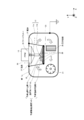
- FIG. 1 schematically shows the configuration of a discharge excitation gas laser apparatus.
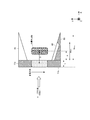
- FIG. 2 shows a view of the laser chamber shown in FIG. 1 viewed from the Z-axis direction.
- FIG. 3 is a view for explaining the state of arc discharge generated in the laser chamber shown in FIG.
- FIG. 4 schematically shows a configuration of a discharge excitation gas laser apparatus including the laser chamber of the present embodiment including the second insulating member.
- FIG. 5 is a view for explaining the first embodiment of the second insulating member.
- FIG. 6 is a view for explaining the size of the second insulating member shown in FIG.
- FIG. 7 is a view for explaining a second embodiment of the second insulating member.
- FIG. 1 schematically shows the configuration of a discharge excitation gas laser apparatus.
- FIG. 2 shows a view of the laser chamber shown in FIG. 1 viewed from the Z-axis direction.
- FIG. 3 is a view for explaining the state of arc discharge generated in the laser chamber shown in FIG.
- FIG. 8 is a view for explaining a third embodiment of the second insulating member.
- FIG. 9 is a view for explaining a fourth embodiment of the second insulating member.
- FIG. 10 is a view for explaining a fifth embodiment of the second insulating member.
- FIG. 11 is a view for explaining a sixth embodiment of the second insulating member.
- FIG. 12A is a diagram for explaining a current path of arc discharge when arc discharge occurs in a conventional laser chamber not including the second insulating member.
- FIG. 12B is a diagram for explaining a current path of the arc discharge when the arc discharge occurs in the laser chamber of the present embodiment including the second insulating member.
- FIG. 12A is a diagram for explaining a current path of arc discharge when arc discharge occurs in a conventional laser chamber not including the second insulating member.
- FIG. 12B is a diagram for explaining a current path of the arc discharge when the arc discharge occurs in the laser chamber of the present embodiment including the second insulating
- FIG. 13 shows a comparison of the transition of the arc insulation distance according to the rotational speed of the fan between the conventional laser chamber shown in FIG. 12A and the laser chamber of the present embodiment shown in FIG. 12B.
- FIG. 14 is a diagram for explaining a circuit configuration of a charge / discharge circuit used in the discharge excitation gas laser apparatus.
- FIG. 15 shows a block diagram of the hardware environment of each control unit.
- the laser chamber 10 is a laser chamber of the discharge excitation gas laser device 1, and is disposed in the laser chamber 10 so as to face the first discharge electrode 11 a in the laser chamber 10.
- the second discharge electrode 11b, the fan 21 for flowing the laser gas between the first discharge electrode 11a and the second discharge electrode 11b, and the first insulation disposed on the upstream side and the downstream side of the laser gas flow in the first discharge electrode 11a A member 20, a metal damper member 50 disposed on the upstream side of the laser gas flow in the second discharge electrode 11b, and a second insulating member 60 disposed on the downstream side of the laser gas flow in the second discharge electrode 11b. Also good. With such a configuration, the laser chamber 10 can perform a stable discharge.
- optical path is a path through which pulsed laser light passes.
- the optical path may be an axis that passes through the center of the beam cross section of the pulse laser beam along the traveling direction of the pulse laser beam.
- FIG. 1 schematically shows the configuration of a discharge excitation gas laser device 1.
- FIG. 2 shows a view of the laser chamber 10 shown in FIG. 1 viewed from the Z-axis direction.
- the laser oscillation direction of the discharge excitation type gas laser device 1 is taken as the Z axis. That is, the direction in which the pulse laser beam is led out from the chamber 10 to the exposure apparatus 110 is taken as the Z axis.
- the X axis and the Y axis are orthogonal to the Z axis and orthogonal to each other.
- the subsequent drawings are the same as the coordinate axes in FIG.
- the discharge excitation gas laser device 1 may be an excimer laser device.
- the laser gas that is a laser medium may be configured using argon or krypton as a rare gas, fluorine as a halogen gas, neon or helium as a buffer gas, or a mixed gas thereof.
- the discharge excitation gas laser apparatus 1 includes a laser chamber 10, a laser resonator, a charger 12, a pulse power module (PPM) 13, a pressure sensor 16, a pulse energy measuring device 17, and a motor 22. And a laser gas supply unit 23, a laser gas discharge unit 24, and a control unit 30.
- PPM pulse power module
- the laser chamber 10 may be filled with a laser gas.
- the laser chamber 10 includes a main discharge portion 11, a preionization discharge portion 40, a window 10a and a window 10b, a plate 25, a wiring 27, a feedthrough 28, a first insulating member 20, and a metal damper member 50.
- the fan 21 may be included.
- the main discharge part 11 may include a first discharge electrode 11a and a second discharge electrode 11b.
- the first discharge electrode 11a and the second discharge electrode 11b may be a pair of electrodes for exciting the laser gas by main discharge.
- the main discharge may be a glow discharge.
- the first discharge electrode 11a and the second discharge electrode 11b may each be formed of a plate-like conductive member.
- the first discharge electrode 11a and the second discharge electrode 11b may be arranged to face each other such that they are separated from each other by a predetermined distance and their longitudinal directions are substantially parallel to each other.
- the first discharge electrode 11a and the second discharge electrode 11b may be arranged with their discharge surfaces facing each other.
- the space between the discharge surface of the first discharge electrode 11a and the discharge surface of the second discharge electrode 11b is also referred to as “discharge space”.
- Laser gas enclosed in the laser chamber 10 may exist in the discharge space.
- a main discharge can occur in the discharge space.
- the first discharge electrode 11a may be a cathode electrode.
- the surface of the first discharge electrode 11 a opposite to the discharge surface may be connected to the pulse power module 13 via the feedthrough 28.
- a pulse voltage can be applied from the pulse power module 13 between the first discharge electrode 11a and the second discharge electrode 11b.
- a side surface of the first discharge electrode 11 a may be surrounded by a first insulating member 20 fixed to the wall 10 c of the laser chamber 10.
- the first discharge electrode 11 a can be electrically insulated from the wall 10 c by the first insulating member 20.
- the second discharge electrode 11b may be an anode electrode.
- the surface of the second discharge electrode 11b opposite to the discharge surface may be fixed to the plate 25.
- the side surface of the second discharge electrode 11 b may be surrounded by a metal damper member 50 fixed to the plate 25.
- the plate 25 may be formed of a conductive member.
- the plate 25 may be fixed to the wall 10c of the laser chamber 10c.
- the plate 25 may be connected to the grounded wall 10 c via the wiring 27.
- the plate 25 can be kept at ground potential.
- the preionization discharge part 40 may be an electrode for preionizing the laser gas by corona discharge as a pre-stage of the main discharge by the main discharge part 11.
- the preliminary ionization discharge part 40 may be fixed to the plate 25.
- the preliminary ionization discharge unit 40 may be disposed on the upstream side of the laser gas flow with respect to the second discharge electrode 11b.
- the periphery of the preliminary ionization discharge part 40 may be surrounded by a metal damper member 50 fixed to the plate 25.
- the preionization discharge unit 40 may include a preionization inner electrode 41, a dielectric pipe 42, and a preionization outer electrode 43.
- the dielectric pipe 42 may be formed in a cylindrical shape.
- the dielectric pipe 42 may be arranged such that the longitudinal direction of the dielectric pipe 42 and the longitudinal direction of the main discharge part 11 are substantially parallel.
- the preionization inner electrode 41 may be formed in a rod shape.
- the preliminary ionization inner electrode 41 may be inserted inside the dielectric pipe 42 and fixed to the inner peripheral surface of the dielectric pipe 42.
- the end of the preionized inner electrode 41 may be connected to the pulse power module 13 via the feedthrough 28.
- the preliminary ionization outer electrode 43 may be formed in a plate shape having a bent portion.
- the preliminary ionization outer electrode 43 may be arranged so that the longitudinal direction of the preliminary ionization outer electrode 43 and the longitudinal direction of the dielectric pipe 42 are substantially parallel.
- the side surface in the longitudinal direction of the preionization outer electrode 43 may be fixed to the outer peripheral surface of the dielectric pipe 42 and the plate 25.
- the first insulating member 20 may electrically insulate between the first discharge electrode 11 a that is a cathode electrode and the wall 10 c of the laser chamber 10.
- the first insulating member 20 may be formed using an insulating material having low reactivity with the laser gas. If the laser gas is fluorine, the first insulating member 20 may be formed using alumina ceramics, for example.
- the first insulating member 20 may be provided so as to surround the side surfaces of the first discharge electrode 11 a and the feedthrough 28.
- the first insulating member 20 may be fixed to the wall 10 c of the laser chamber 10. Accordingly, the first insulating member 20 may hold the first discharge electrode 11a and the feedthrough 28 on the wall 10c.
- the first insulating member 20 may be disposed on the upstream side and the downstream side of the laser gas flow in the first discharge electrode 11a.
- a part of the first insulating member 20 located on the upstream side of the first discharge electrode 11a may have a tapered surface that becomes thicker from the upstream side toward the downstream side.
- a part of the first insulating member 20 located on the downstream side of the first discharge electrode 11a may have a tapered surface that becomes thinner from the upstream side toward the downstream side.
- the metal damper member 50 may absorb acoustic waves generated with the main discharge.
- the metal damper member 50 may be formed using a porous metal material having low reactivity with the laser gas. If the laser gas is fluorine, the metal damper member 50 may be formed using a material such as nickel or a nickel chromium alloy. Thereby, the metal damper member 50 can absorb most of the acoustic waves generated with the main discharge.
- the metal damper member 50 may be provided so as to surround the side surfaces of the second discharge electrode 11b and the preliminary ionization discharge part 40.
- the metal damper member 50 may be fixed to the plate 25. Accordingly, the metal damper member 50 may hold the second discharge electrode 11b and the preliminary ionization discharge part 40 on the plate 25.
- the metal damper member 50 is formed using a porous metal material, generation of debris, dust, and the like due to an acoustic wave impact can be suppressed. If the metal damper member 50 is formed using a porous ceramic material or resin material instead of a porous metal material, debris, dust, or the like may be generated from the ceramic material or resin material due to the impact of an acoustic wave. When debris, dust, or the like is generated in the laser chamber 10, the discharge becomes unstable, and the pulse energy of the pulse laser beam can be reduced. Therefore, it is preferable that the metal damper member 50 is formed using a porous metal material.
- the metal damper member 50 disposed around the second discharge electrode 11b is formed using a porous metal material.
- the discharge direction of the main discharge is a direction from the first discharge electrode 11a that is the cathode electrode toward the second discharge electrode 11b that is the anode electrode.
- the impact force of the acoustic wave generated along with the main discharge can be larger on the anode electrode side that is the distal end side in the discharge direction than on the cathode electrode side that is the proximal end side in the discharge direction.
- the metal damper member 50 is formed using a porous metal material.
- the metal damper member 50 may be disposed at least on the upstream side of the laser gas flow in the second discharge electrode 11b.
- the metal damper member 50 may be disposed on the upstream side and the downstream side of the laser gas flow in the second discharge electrode 11b.
- a part of the metal damper member 50 located on the upstream side of the second discharge electrode 11b may have a tapered surface that becomes thicker from the upstream side toward the downstream side.
- a part of the metal damper member 50 located on the downstream side of the second discharge electrode 11b may have a tapered surface that becomes thinner from the upstream side toward the downstream side. Accordingly, the laser gas can be guided to the tapered surface of the metal damper member 50 and can efficiently flow between the first discharge electrode 11a and the second discharge electrode 11b. Furthermore, a part of the acoustic wave generated along with the main discharge can be reflected away from the discharge space by the tapered surface of the metal damper member 50.
- the fan 21 may circulate laser gas in the laser chamber 10.
- the fan 21 may be a cross flow fan.
- the fan 21 may be arranged such that the longitudinal direction of the first discharge electrode 11a and the second discharge electrode 11b and the longitudinal direction of the fan 21 are substantially parallel.
- the fan 21 may be disposed on the opposite side of the discharge space with respect to the plate 25.
- the fan 21 may rotate by driving the motor 22.
- the rotating fan 21 may generate a laser gas flow.
- the laser gas in the laser chamber 10 can blow out substantially uniformly in a direction perpendicular to the longitudinal direction of the fan 21.
- the laser gas blown out from the fan 21 can flow into the discharge space.
- the flow direction of the laser gas flow flowing into the discharge space may be a direction perpendicular to the longitudinal direction of the first discharge electrode 11a and the second discharge electrode 11b.
- the laser gas that has flowed into the discharge space can flow out of the discharge space.
- the flow direction of the laser gas flow flowing out from the discharge space may be a direction perpendicular to the longitudinal direction of the first discharge electrode 11a and the second discharge electrode 11b.
- the laser gas flowing out from the discharge space can be sucked into the fan 21 through the heat exchanger 26.
- the heat exchanger 26 may perform heat exchange between the refrigerant supplied into the heat exchanger 26 and the laser gas.
- the supply amount of the refrigerant supplied to the inside of the heat exchanger 26 may be changed by control from the control unit 30.
- the heat transfer amount from the laser gas to the refrigerant may fluctuate. Thereby, the laser gas temperature in the laser chamber 10 can be adjusted.
- the motor 22 may rotate the fan 21.
- the motor 22 may be a stepping motor or a servo motor.
- the motor 22 may change the rotation speed of the fan 21 under the control of the control unit 30.
- the charger 12 may be configured by a capacitor or the like connected to a power supply device (not shown).
- the charger 12 can hold electric energy for applying a voltage to the main discharge unit 11.
- the charger 12 may output the electric energy to the pulse power module 13 under the control of the control unit 30.
- the pulse power module 13 may apply a voltage to the main discharge part 11 and the preliminary ionization discharge part 40.
- the pulse power module 13 may include a switch 13 a controlled by the control unit 30. When the switch 13 a is turned from OFF to ON, the pulse power module 13 may generate a pulsed voltage from the electric energy held in the charger 12. The pulse power module 13 may apply the generated pulse voltage to the main discharge unit 11 and the preliminary ionization discharge unit 40.
- the charge / discharge circuit of the discharge excitation type gas laser apparatus 1 including the main discharge unit 11, the preliminary ionization discharge unit 40, the charger 12, and the pulse power module 13 will be described later with reference to FIG.
- the laser resonator may be configured by a line narrowing module (LNM) 14 and an output coupler (OC) 15.
- the narrow band module 14 may include a prism 14a and a grating 14b.
- the prism 14a may expand the beam width of the light emitted from the laser chamber 10 through the window 10a.
- the prism 14a may transmit the enlarged light to the grating 14b side.
- Light that passes through the prism 14a toward the grating 14b can be refracted at different angles depending on the wavelength of the light.
- the prism 14a can also function as a wavelength dispersion element.
- the grating 14b may be a wavelength dispersion element in which a number of grooves are formed on the surface at predetermined intervals.
- the grating 14b may have a Littrow arrangement in which the incident angle and the diffraction angle are the same.
- the grating 14b may be formed of a highly reflective material.
- Each groove formed in the grating 14b may be, for example, a triangular groove.
- the light that has entered the grating 14b from the prism 14a can be reflected in multiple directions perpendicular to the direction in which each groove extends on the slope of each groove. The direction in which each groove extends may correspond to the Y direction in FIG.
- the optical path length difference between the reflected lights can depend on the reflection angle of the reflected light.
- the light of the wavelength corresponding to the optical path length difference can be strengthened because the phases of the reflected lights coincide with each other.
- light having a wavelength that does not correspond to the optical path length difference can be weakened because the phases of the reflected light do not match.
- the grating 14b can selectively extract light near a specific wavelength according to the reflection angle. The light near the specific wavelength can return to the laser chamber 10 from the grating 14b through the prism 14a and the window 10a. Thereby, the spectral width of the light returned from the grating 14b to the laser chamber 10 can be narrowed.
- the output coupling mirror 15 may transmit a part of the light emitted from the laser chamber 10 and reflect the other part to return to the laser chamber 10.
- the surface of the output coupling mirror 15 may be coated with a partial reflection film.
- the distance between the output coupling mirror 15 and the grating 14b may be set to a distance at which the light emitted from the laser chamber 10 forms a standing wave. Thereby, the output coupling mirror 15 and the narrow-band module 14 can constitute a laser resonator.
- the light emitted from the laser chamber 10 can reciprocate between the band narrowing module 14 and the output coupling mirror 15. At this time, the light emitted from the laser chamber 10 can be amplified every time it passes through the main discharge part 11 in the laser chamber 10. A part of the amplified light may pass through the output coupling mirror 15. The light transmitted through the output coupling mirror 15 can be output to the exposure apparatus 110 via the pulse energy measuring device 17 as pulse laser light.
- the pulse energy measuring device 17 may measure the pulse energy of the pulse laser beam that has passed through the output coupling mirror 15 and output the measurement result to the control unit 30.
- the pulse energy measuring device 17 may include a beam splitter 17a, a condensing lens 17b, and an optical sensor 17c.
- the beam splitter 17a may be disposed on the optical path of the pulse laser beam.
- the beam splitter 17a may transmit the pulsed laser light transmitted through the output coupling mirror 15 toward the exposure apparatus 110 with high transmittance.
- the beam splitter 17a may reflect part of the pulsed laser light that has passed through the output coupling mirror 15 toward the condenser lens 17b.
- the condensing lens 17b may condense the pulsed laser light reflected by the beam splitter 17a on the light receiving surface of the optical sensor 17c.
- the optical sensor 17c may detect the pulse laser beam condensed on the light receiving surface.
- the optical sensor 17c may measure the pulse energy of the detected pulse laser beam.
- the optical sensor 17 c may output a signal related to the measured pulse energy to the control unit 30.
- the pressure sensor 16 may detect the gas pressure in the laser chamber 10.
- the pressure sensor 16 may output a detection signal of the detected gas pressure to the control unit 30.
- the laser gas supply unit 23 may supply laser gas into the laser chamber 10.
- the laser gas supply unit 23 may include a gas cylinder (not shown), a valve, and a flow rate control valve.
- the gas cylinder may be filled with laser gas.
- the valve may block the flow of laser gas from the gas cylinder into the laser chamber 10.
- the flow control valve may vary the supply amount of the laser gas from the gas cylinder into the laser chamber 10.
- the laser gas supply unit 23 may open and close the valve under the control of the control unit 30.
- the laser gas supply unit 23 may vary the opening degree of the flow control valve under the control of the control unit 30.
- the opening degree of the flow control valve varies, the supply amount of the laser gas into the laser chamber 10 may vary. Thereby, the gas pressure in the laser chamber 10 can be adjusted.
- the laser gas discharge unit 24 may discharge the laser gas in the laser chamber 10 to the outside of the laser chamber 10.
- the laser gas discharge unit 24 may include a valve (not shown) and an exhaust pump.
- the valve may block the flow of laser gas from inside the laser chamber 10 to the outside of the laser chamber 10.
- the exhaust pump may suck the laser gas in the laser chamber 10.
- the laser gas discharge unit 24 may open and close the valve under the control of the control unit 30.
- the laser gas discharge unit 24 may operate the exhaust pump under the control of the control unit 30.
- the exhaust pump When the exhaust pump is activated, the laser gas in the laser chamber 10 can be sucked into the exhaust pump. Thereby, the laser gas in the laser chamber 10 is discharged out of the laser chamber 10, and the gas pressure in the laser chamber 10 can be reduced.
- the control unit 30 may transmit and receive various signals to and from the exposure apparatus control unit 111 provided in the exposure apparatus 110. For example, a signal related to the target pulse energy or target oscillation timing of the pulse laser beam output to the exposure apparatus 110 may be transmitted from the exposure apparatus control unit 111 to the control unit 30.
- the control unit 30 may comprehensively control the operation of each component of the discharge excitation gas laser apparatus 1 based on various signals transmitted from the exposure apparatus control unit 111.
- a signal related to pulse energy output from the pulse energy measuring device 17 may be input to the control unit 30.
- the control unit 30 may determine the charging voltage of the charger 12 based on the signal related to the pulse energy and the signal related to the target pulse energy from the exposure apparatus control unit 111.
- the control unit 30 may output a control signal corresponding to the determined charging voltage to the charger 12.
- the control signal may be a signal for controlling the operation of the charger 12 such that the determined charging voltage is set in the charger 12.
- the control unit 30 may determine the timing for applying the pulse voltage to the main discharge unit 11 based on the signal related to the pulse energy from the pulse energy measuring device 17 and the signal related to the target oscillation timing from the exposure apparatus control unit 111.
- the control unit 30 may output an oscillation trigger signal corresponding to the determined timing to the pulse power module 13.
- the oscillation trigger signal may be a control signal for controlling the operation of the pulse power module 13 so that the switch 13a is turned on or off according to the determined timing.
- a gas pressure detection signal output from the pressure sensor 16 may be input to the control unit 30.
- the control unit 30 may determine the gas pressure of the laser gas in the laser chamber 10 based on the gas pressure detection signal and the charging voltage of the charger 12.
- the control unit 30 may output a control signal corresponding to the determined gas pressure to the laser gas supply unit 23 or the laser gas discharge unit 24.
- the control signal may be a signal for controlling the operation of the laser gas supply unit 23 or the laser gas discharge unit 24 so that the laser gas is supplied or discharged into the laser chamber 10 according to the determined gas pressure.
- the control unit 30 may drive the motor 22 and rotate the fan 21. Thereby, the laser gas in the laser chamber 10 can circulate.
- the control unit 30 may receive a signal regarding the target pulse energy Et and the target oscillation timing transmitted from the exposure apparatus control unit 111.
- the control unit 30 may set the charging voltage Vhv corresponding to the target pulse energy Et in the charger 12.
- the control unit 30 may store the value of the charging voltage Vhv set in the charger 12.
- the control unit 30 may operate the switch 13a of the pulse power module 13 in synchronization with the target oscillation timing.
- a voltage can be applied between the preionization inner electrode 41 and the preionization outer electrode 43 of the preionization discharge unit 40.
- a voltage may be applied between the first discharge electrode 11a and the second discharge electrode 11b of the main discharge part 11.
- UV Ultraviolet
- the laser gas can be preionized.
- main discharge can occur in the discharge space of the main discharge portion 11.
- the discharge direction of the main discharge is a direction from the first discharge electrode 11a that is the cathode electrode toward the second discharge electrode 11b that is the anode electrode.
- the light emitted from the laser gas is reflected by the narrowband module 14 and the output coupling mirror 15 constituting the laser resonator, and can reciprocate in the laser resonator.
- the light traveling back and forth within the laser resonator can be narrowed by the narrowing module 14.
- the light traveling back and forth in the laser resonator can be amplified every time it passes through the main discharge part 11. Thereafter, a part of the amplified light can pass through the output coupling mirror 15.
- the light transmitted through the output coupling mirror 15 can be output to the exposure apparatus 110 as pulse laser light.
- a part of the pulse laser beam transmitted through the output coupling mirror 15 may be incident on the pulse energy measuring device 17.
- the pulse energy measuring device 17 may measure the pulse energy E of the incident pulse laser light and output it to the control unit 30.
- the control unit 30 may store the pulse energy E measured by the pulse energy measuring device 17.
- the control unit 30 may calculate a difference ⁇ E between the pulse energy E, which is a measured value, and the target pulse energy Et.
- the control unit 30 may calculate an increase / decrease amount ⁇ Vhv of the charging voltage Vhv corresponding to the difference ⁇ E.
- the control unit 30 may calculate the newly set charging voltage Vhv by adding the calculated ⁇ Vhv to the charging voltage Vhv stored above. In this way, the control unit 30 can feedback control the charging voltage Vhv.
- the control unit 30 controls the laser gas supply unit 23 to supply laser gas into the laser chamber 10 until a predetermined gas pressure is reached. May be.
- the control unit 30 controls the laser gas discharge unit 24 to discharge the laser gas from the laser chamber 10 until a predetermined gas pressure is reached. It may be discharged.
- a discharge product can be generated in the discharge space by the main discharge.
- the discharge product may be ions or active species generated when the laser gas is ionized by the main discharge.
- the discharge product generated in the discharge space can move from the discharge space to the downstream side of the laser gas flow by the laser gas flow generated by the rotation of the fan 21.
- the rotation speed of the fan 21 when the fan 21 is rotated while suppressing power consumption, or when the fan 21 is started or stopped, the rotation speed of the fan 21 may be lower than that in a steady state.
- the rotational speed of the fan 21 is decreased, the flow velocity of the laser gas flow passing through the discharge space can be decreased.
- the discharge product may stay in the vicinity of the main discharge portion 11 without being sufficiently separated from the discharge space by the laser gas flow.
- the discharge product has a lower discharge resistance than the non-ionized laser gas.
- the main discharge of the main discharge part 11 can be a discharge from the first discharge electrode 11a toward the second discharge electrode 11b through the discharge product.
- the discharge is arc discharge, and unlike glow discharge, which is normal main discharge, excessive current flows and can be unstable.
- the main discharge of the main discharge part 11 can be a discharge from the first discharge electrode 11a toward the metal damper member 50 through the discharge product. As a result, the pulse energy of the pulse laser beam output from the discharge excitation gas laser device 1 can be unstable.
- the laser chamber 10 according to the present embodiment including the second insulating member will be described with reference to FIGS.
- the laser chamber 10 of this embodiment may have a configuration in which a second insulating member 60 is added to the laser chamber 10 shown in FIGS. 1 and 2.
- the configuration other than the second insulating member 60 may be the same as that of the laser chamber 10 shown in FIGS. 1 and 2.
- the description of the same configuration as the laser chamber 10 shown in FIGS. 1 and 2 is omitted.
- Embodiments of the second insulating member 60 included in the laser chamber 10 of the present embodiment will be described as first to sixth embodiments.
- FIG. 4 schematically shows the configuration of the discharge excitation gas laser apparatus 1 including the laser chamber 10 of the present embodiment including the second insulating member.
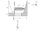
- FIG. 5 is a view for explaining the first embodiment of the second insulating member 60.
- FIG. 5 shows the metal damper member 50 and the second insulating member 60 disposed on the downstream side of the laser gas flow in the second discharge electrode 11b.
- the second insulating member 60 may suppress the discharge from the first discharge electrode 11a toward the second discharge electrode 11b through the discharge product.
- the second insulating member 60 may suppress the discharge from the first discharge electrode 11a toward the metal damper member 50 through the discharge product.
- the second insulating member 60 may be formed using an insulating material having low reactivity with the laser gas. If the laser gas is fluorine, the first insulating member 20 may be formed using alumina ceramics, for example.
- the second insulating member 60 may be disposed on the downstream side of the laser gas flow in the second discharge electrode 11b. The second insulating member 60 may extend toward the downstream side of the laser gas flow with the side surface of the second discharge electrode 11b on the downstream side of the laser gas flow as a base end.
- the second insulating member 60 may be disposed on the tapered surface of the metal damper member 50 on the downstream side of the laser gas flow with respect to the second discharge electrode 11b along the inclination of the tapered surface.
- the second insulating member 60 can form a tapered surface that becomes thinner from the upstream side toward the downstream side.
- the second insulating member 60 may be disposed so as to face the discharge product staying in the vicinity of the main discharge portion 11.
- FIG. 6 is a view for explaining the size of the second insulating member 60 shown in FIG.
- the width of the second discharge electrode 11b in the flow direction of the laser gas flow is L.
- W be the length of the width of the second insulating member 60 in the flow direction of the laser gas flow.
- W min and W max be the minimum and maximum values of the width W of the second insulating member 60.
- D be the moving distance of the discharge product moved from the discharge space in the flow direction of the laser gas flow.
- A be the distance from the side surface of the second discharge electrode 11b on the downstream side of the laser gas flow to the center of the discharge product.
- the length L of the width of the second discharge electrode 11b, the movement distance D of the discharge product, and the length W of the width of the second insulating member 60 are the longitudinal direction of the first discharge electrode 11a and the second discharge electrode 11b, and It may be a length in a direction perpendicular to the discharge direction.
- the velocity of the laser gas flow be v.
- the flow velocity v may be a predetermined speed so that dielectric breakdown does not occur between the first discharge electrode 11a and the second discharge electrode 11b and the discharge product.
- the repetition frequency of the discharge excitation type gas laser device 1 is assumed to be f.
- the travel distance D of the discharge product may be calculated from the following equation.
- D v / f
- the distance A from the downstream side surface of the second discharge electrode 11b to the discharge product may be calculated from the following equation.
- A DL / 2
- the second insulating member 60 includes the metal damper member 50 that discharges from the first discharge electrode 11a toward the second discharge electrode 11b via the discharge product and from the first discharge electrode 11a via the discharge product. You may suppress the discharge which goes to.
- the width W of the second insulating member 60 is from the downstream side surface of the second discharge electrode 11b to the discharge product. If it is more than the distance A, it can be suppressed.
- the discharge from the first discharge electrode 11a toward the metal damper member 50 through the discharge product is such that the length W of the width of the second insulating member 60 is the discharge product from the downstream side surface of the second discharge electrode 11b.
- the second insulating member 60 may be less likely to absorb acoustic waves than the metal damper member 50. Therefore, the acoustic wave may be reflected by the second insulating member 60 and return to the discharge space again.
- the density of the laser gas in the discharge space becomes non-uniform and the discharge product may stay in the vicinity of the main discharge portion 11.
- the discharge can be started in a state where the laser gas is unevenly distributed or in a state where the discharge product stays in the vicinity of the main discharge portion 11.
- the width W of the second insulating member 60 in the laser gas flow direction may satisfy the relationship of the following equation.
- the laser chamber 10 including the second insulating member 60 of the first embodiment generates debris and dust due to the impact of the acoustic wave, uneven distribution of the laser gas due to the reflection of the acoustic wave, retention of the discharge product, and discharge product. It is possible to solve the problems of arc discharge via For this reason, the laser chamber 10 including the second insulating member 60 of the first embodiment can perform stable discharge even when the rotational speed of the fan 21 is reduced.
- Other configurations of the laser chamber 10 including the second insulating member 60 of the first embodiment may be the same as the configurations of the laser chamber 10 shown in FIGS. 1 and 2.
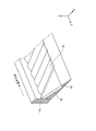
- FIG. 7 is a view for explaining a second embodiment of the second insulating member 60.
- FIG. 7 shows the metal damper member 50 and the second insulating member 60 disposed on the downstream side of the laser gas flow in the second discharge electrode 11b. The same applies to FIGS.
- the second insulating member 60 of the second embodiment may have a configuration in which a recess 61 is added to the second insulating member 60 of the first embodiment shown in FIGS. 4 to 6.
- the recess 61 may be formed on the surface of the second insulating member 60.
- the concave portion 61 may be formed to be inclined and extend with respect to a direction perpendicular to the longitudinal direction of the second discharge electrode 11b.
- the direction perpendicular to the longitudinal direction of the second discharge electrode 11b may include the flow direction of the laser gas flow and the discharge direction.
- the recess 61 may be formed so as to extend obliquely with respect to the flow direction of the laser gas flow, which is a direction perpendicular to the longitudinal direction of the second discharge electrode 11b.
- the recess 61 may be formed so as to extend obliquely with respect to the discharge direction which is a direction perpendicular to the longitudinal direction of the second discharge electrode 11b.
- the recess 61 may be formed along the tapered surface of the metal damper member 50 located on the downstream side of the second discharge electrode 11b.
- the cross-sectional shape of the recess 61 viewed from the direction in which the recess 61 extends may be formed in a rectangular wave shape.
- the acoustic wave generated in the discharge space When the acoustic wave generated in the discharge space is reflected by the second insulating member 60, it can be reflected in various directions by the recess 61.
- the reflected waves reflected in various directions by the recess 61 have various phases and can weaken each other.
- the concave portion 61 is formed to be inclined with respect to a direction perpendicular to the longitudinal direction of the second discharge electrode 11b, the acoustic wave is reflected by the concave portion 61 in a more complicated direction and can be further weakened. For this reason, the acoustic wave generated in the discharge space may be difficult to return to the discharge space again after being reflected by the second insulating member 60 in which the recess 61 is formed.
- the laser chamber 10 including the second insulating member 60 of the second embodiment can perform more stable discharge than the laser chamber 10 including the second insulating member 60 of the first embodiment.
- Other configurations of the laser chamber 10 including the second insulating member 60 of the second embodiment may be the same as the configurations of the laser chamber 10 including the second insulating member 60 of the first embodiment.
- FIG. 8 is a view for explaining a third embodiment of the second insulating member 60.
- the shape of the recess 61 included in the second insulating member 60 of the third embodiment may be different from the shape of the recess 61 included in the second insulating member 60 of the second embodiment shown in FIG. .
- the cross-sectional shape of the recess 61 viewed from the direction in which the recess 61 extends may be formed in a triangular wave shape or a sawtooth wave shape.
- the laser chamber 10 including the second insulating member 60 of the third embodiment can perform a stable discharge in the same manner as the laser chamber 10 including the second insulating member 60 of the second embodiment.
- Other configurations of the laser chamber 10 including the second insulating member 60 of the third embodiment may be the same as the configurations of the laser chamber 10 including the second insulating member 60 of the second embodiment.
- FIG. 9 is a view for explaining a fourth embodiment of the second insulating member 60.
- the shape of the recess 61 included in the second insulating member 60 of the fourth embodiment may be different from the shape of the recess 61 included in the second insulating member 60 of the second embodiment shown in FIG. .
- the cross-sectional shape of the recess 61 viewed from the direction in which the recess 61 extends may be formed in a semicircular wave shape.
- the semicircular wave shape may be a shape in which semicircles are periodically connected.
- the laser chamber 10 including the second insulating member 60 of the fourth embodiment can perform a stable discharge in the same manner as the laser chamber 10 including the second insulating member 60 of the second embodiment.
- Other configurations of the laser chamber 10 including the second insulating member 60 of the fourth embodiment may be the same as the configurations of the laser chamber 10 including the second insulating member 60 of the second embodiment.
- FIG. 10 is a view for explaining the fifth embodiment of the second insulating member 60.
- the shape of the recess 61 included in the second insulating member 60 of the fifth embodiment may be different from the shape of the recess 61 included in the second insulating member 60 of the second embodiment shown in FIG. .
- the recess 61 may be formed in a shape in which a large number of one hemispherical dimple is provided.
- the laser chamber 10 including the second insulating member 60 of the fifth embodiment can perform a stable discharge in the same manner as the laser chamber 10 including the second insulating member 60 of the second embodiment.
- Other configurations of the laser chamber 10 including the second insulating member 60 of the fifth embodiment may be the same as the configurations of the laser chamber 10 including the second insulating member 60 of the second embodiment.
- FIG. 11 is a view for explaining a sixth embodiment of the second insulating member 60.
- the constituent material of the second insulating member 60 of the sixth embodiment may be a material different from the constituent material of the second insulating member 60 of the first embodiment shown in FIGS. 4 to 6.
- the constituent material of the second insulating member 60 of the sixth embodiment is an insulating material having low reactivity with the laser gas, and may be a material having a porous structure like the metal damper member 50.
- the second insulating member 60 of the sixth embodiment can absorb acoustic waves even by the second insulating member 60 itself. Thereby, the laser chamber 10 including the second insulating member 60 of the sixth embodiment can perform more stable discharge than the laser chamber 10 including the second insulating member 60 of the first embodiment.
- Other configurations of the laser chamber 10 including the second insulating member 60 of the sixth embodiment may be the same as the configurations of the laser chamber 10 including the second insulating member 60 of the first embodiment.
- the repetition frequency of the discharge excitation type gas laser device 1 may be about 6 kHz, for example.
- the flow velocity v of the laser gas flow may be 40 m / s to 45 m / s, for example.
- the travel distance D of the discharge product shown in FIG. 6 may be, for example, 6.7 to 7.5 mm.
- the second insulating member 60 and the metal damper member 50 may be formed as follows.
- the second insulating member 60 may be formed such that the width length W in the laser gas flow direction is, for example, about 16 mm.
- the width length W of the second insulating member 60 in the laser gas flow direction can satisfy the relationship of (2v / f) ⁇ L ⁇ W ⁇ c / 2f as described above with reference to FIG.
- the surface of the second insulating member 60 may be a flat surface.
- the metal damper member 50 located on the downstream side of the second discharge electrode 11b may be formed so that the width in the laser gas flow direction is, for example, about 50 mm. Note that the metal damper member 50 located downstream of the second discharge electrode 11b extends further to the downstream side of the second insulating member 60 in the flow direction of the laser gas flow, as shown in FIG. May be formed. Thereby, the metal damper member 50 can absorb the acoustic wave generated along with the main discharge and suppress the adverse effects of the acoustic wave such as uneven distribution of laser gas and stagnation of discharge products.
- FIG. 12A is a diagram for explaining a current path of arc discharge when arc discharge occurs in the conventional laser chamber 10 that does not include the second insulating member 60.
- FIG. 12B is a diagram for explaining a current path of the arc discharge when the arc discharge is generated in the laser chamber 10 of the present embodiment including the second insulating member 60.
- the abnormal arc discharge generated on the downstream side of the laser gas flow can be a discharge from the first discharge electrode 11a toward the second discharge electrode 11b through the discharge product.
- the arc discharge can be suppressed as the insulation distance in the current path is longer.
- the insulation distance in the current path of arc discharge from the first discharge electrode 11a to the second discharge electrode 11b through the discharge product is also referred to as “arc insulation distance”.
- the conventional laser chamber 10 does not include the second insulating member 60. Therefore, the current path P of the arc discharge can be formed so as to go from the first discharge electrode 11a to the metal damper member 50 through the discharge product, as shown in FIG. 12A.
- the current path P of the arc discharge includes the current path P1 from the first discharge electrode 11a to the discharge product, the current path P2 in the discharge product, and the discharge product to the metal damper member 50.
- the current path P3 may be included. Therefore, in the conventional laser chamber 10, the arc insulation distance p in the current path P of the arc discharge can correspond to the total length of the current path P1 and the current path P3.
- the laser chamber 10 of the present embodiment may include the second insulating member 60. Therefore, the current path Q of the arc discharge can be formed so as to go from the first discharge electrode 11a to the second discharge electrode 11b through the discharge product as shown in FIG. 12B.
- the current path Q of the arc discharge includes a current path Q1 from the first discharge electrode 11a to the discharge product, a current path Q2 in the discharge product, and from the discharge product to the second discharge electrode 11b.
- FIG. 13 is a graph comparing the transition of the arc insulation distance according to the rotation speed of the fan 21 between the conventional laser chamber 10 shown in FIG. 12A and the laser chamber 10 of the present embodiment shown in FIG. 12B. Show.
- the length of the current path of the arc discharge generated on the downstream side of the laser gas flow can be increased in both the conventional and the laser chamber 10 of the present embodiment.
- the arc insulation distance can be increased in both the conventional and the laser chamber 10 of the present embodiment.
- the arc insulation distance q in the laser chamber 10 of the present embodiment is the arc in the conventional laser chamber 10. It can be longer than the insulation distance p.
- the arc insulation distance q in the laser chamber 10 of the present embodiment is about twice as long as the arc insulation distance p in the conventional laser chamber 10. It can be. Therefore, the laser chamber 10 of the present embodiment including the second insulating member 60 can significantly suppress abnormal arc discharge that occurs on the downstream side of the laser gas flow, as compared with the conventional laser chamber 10. Therefore, the stability of the main discharge can be greatly improved in the laser chamber 10 of the present embodiment including the second insulating member 60 as compared with the conventional laser chamber 10.
- the rotational speed of the fan 21 in the laser chamber 10 of the present embodiment is much higher than that of the conventional laser chamber 10. You can get less. Therefore, the laser chamber 10 of this embodiment including the second insulating member 60 can significantly reduce the power consumption of the motor 22 that drives the fan 21 as compared with the conventional laser chamber 10.
- FIG. 14 is a diagram for explaining the circuit configuration of a charge / discharge circuit used in the discharge excitation gas laser apparatus 1.
- Pulse power module 13 includes a semiconductor switch is a switch 13a as described above, a transformer TC 1, a magnetic switch MS 1 ⁇ MS 3, the charging capacitor C 0, the capacitor C 1 ⁇ C 3, may contain.
- the magnetic switch MS 1 ⁇ MS 3 can easily current flows.
- the threshold value may be different for each magnetic switch. In the present embodiment, the state in which the magnetic switches MS 1 to MS 3 are easy to pass a current is also referred to as “the magnetic switch is closed”.
- Switch 13a may be provided between the primary side of the transformer TC 1 and the charging capacitor C 0.
- the magnetic switch MS 1 may be provided between the secondary side of the transformer TC 1 and the capacitor C 1 .
- Magnetic switch MS 2 may be provided between the capacitor C 1 and capacitor C 2.
- Magnetic switch MS 3 may be provided between the capacitor C 2 and the capacitor C 3.
- the primary side and the secondary side of the transformer TC 1 may be electrically insulated. The direction of the primary winding of the transformer TC 1 and the direction of the secondary winding may be opposite to each other.
- the second discharge electrode 11b and the preliminary ionization outer electrode 43 may be grounded.
- Voltage divider circuit including a capacitor C 11 and C 12 and the inductor L 0 is may be connected in parallel with the first discharge electrode 11a and the second discharge electrode 11b.
- Capacitor C 11 and C 12 and the inductor L 0 is may be respectively connected in series.
- the charging voltage Vhv may be set in the charger 12 by the control unit 30.
- Charger 12 based on the set charge voltage Vhv, may charge the charging capacitor C 0.
- An oscillation trigger signal may be output from the control unit 30 to the switch 13 a of the pulse power module 13.
- the pulse power module 13 may turn on the switch 13a.
- the switch 13a is turned ON, a current may flow from the charging capacitor C 0 to the primary side of the transformer TC 1.
- a current flows through the primary side of the transformer TC 1, it may reverse current flows through the secondary side of the transformer TC 1 by electromagnetic induction.
- the time integral value of the voltage applied to the magnetic switch MS 1 may eventually reach a threshold value.
- the magnetic switch MS 1 becomes a state of being magnetically saturated, the magnetic switch MS 1 may close.
- the magnetic switch MS 1 is closed, a current flows from the secondary side of the transformer TC 2 to the capacitor C 1 and the capacitor C 1 can be charged.
- magnetic switch MS 2 By the capacitor C 1 is charged, eventually magnetic switch MS 2 becomes a state of magnetic saturation, magnetic switch MS 2 may close.
- the magnetic switch MS 2 When the magnetic switch MS 2 is closed, a current flows from the capacitor C 1 to capacitor C 2, the capacitor C 2 may be charged. In this case, at a pulse width shorter than the pulse width of the current in charging the capacitor C 1, the capacitor C 2 may be charged.
- the magnetic switch MS 3 By the capacitor C 2 is charged, eventually magnetic switch MS 3 becomes a state of being magnetically saturated, the magnetic switch MS 3 can close.
- the magnetic switch MS 3 When the magnetic switch MS 3 is closed, a current flows from the capacitor C 2 to the capacitor C 3, the capacitor C 3 may be charged. In this case, at a pulse width shorter than the pulse width of the current in charging the capacitor C 2, the capacitor C 3 may be charged.
- the pulse width of the current can be compressed.
- a pulse voltage may be applied by the capacitor C 3.
- the pulse voltage applied between the first discharge electrode 11a and the second discharge electrode 11b is greater than the dielectric strength of the laser gas, the laser gas can be broken down.
- the laser gas is broken down, a main discharge may be generated between the first discharge electrode 11a and the second discharge electrode 11b. At this time, a negative potential may be applied to the first discharge electrode 11a.
- the voltage dividing circuit connected in parallel to the first discharge electrode 11a and the second discharge electrode 11b may divide the pulse voltage applied between the first discharge electrode 11a and the second discharge electrode 11b.
- the divided range may be a range of 25% to 75% of the pulse voltage applied between the first discharge electrode 11a and the second discharge electrode 11b.
- the divided pulse voltage may be applied between the preionization inner electrode 41 and the preionization outer electrode 43.
- Voltage dividing ratio in the voltage divider circuit, the capacitance of the capacitor C 11 and C 12, and by adjusting the inductance of the inductor L 0, the time constant of the voltage divider circuit can be adjusted to the desired value. Thereby, the timing of the preionization discharge with respect to the main discharge can be adjusted.
- the combined capacitance of the voltage divider circuit may be adjusted to less than 10% of the capacity of the capacitor C 3.
- FIG. 15 is a block diagram illustrating an example hardware environment in which various aspects of the disclosed subject matter may be implemented.
- the exemplary hardware environment 100 of FIG. 15 includes a processing unit 1000, a storage unit 1005, a user interface 1010, a parallel I / O controller 1020, a serial I / O controller 1030, A / D, D / A.
- the converter 1040 may be included, the configuration of the hardware environment 100 is not limited to this.
- the processing unit 1000 may include a central processing unit (CPU) 1001, a memory 1002, a timer 1003, and an image processing unit (GPU) 1004.
- the memory 1002 may include random access memory (RAM) and read only memory (ROM).
- the CPU 1001 may be any commercially available processor. A dual microprocessor or other multiprocessor architecture may be used as the CPU 1001.
- FIG. 15 may be interconnected to perform the processes described in this disclosure.
- the processing unit 1000 may read and execute a program stored in the storage unit 1005, or the processing unit 1000 may read data together with the program from the storage unit 1005.
- the unit 1000 may write data to the storage unit 1005.
- the CPU 1001 may execute a program read from the storage unit 1005.
- the memory 1002 may be a work area for temporarily storing programs executed by the CPU 1001 and data used for the operation of the CPU 1001.
- the timer 1003 may measure the time interval and output the measurement result to the CPU 1001 according to the execution of the program.
- the GPU 1004 may process the image data according to a program read from the storage unit 1005 and output the processing result to the CPU 1001.
- the parallel I / O controller 1020 may be connected to a parallel I / O device that can communicate with the processing unit 1000, such as the control unit 30, and controls communication between the processing unit 1000 and these parallel I / O devices. May be.
- the serial I / O controller 1030 is a serial I / O device that can communicate with the processing unit 1000, such as the charger 12, the pulse power module 13, the motor 22, the laser gas supply unit 23, the laser gas exhaust unit 24, and the heat exchanger 26. And communication between the processing unit 1000 and the serial I / O devices may be controlled.
- the A / D and D / A converter 1040 may be connected to analog devices such as a temperature sensor, a pressure sensor 16, various vacuum gauge sensors, and an optical sensor 17c via an analog port. Communication with the device may be controlled, or A / D and D / A conversion of communication content may be performed.
- the user interface 1010 may display the progress of the program executed by the processing unit 1000 to the operator so that the operator can instruct the processing unit 1000 to stop the program or execute the interrupt routine.
- the exemplary hardware environment 100 may be applied to the configuration of the control unit 30 in the present disclosure.
- controllers may be implemented in a distributed computing environment, i.e., an environment where tasks are performed by processing units connected via a communications network.
- the control units 30 may be connected to each other via a communication network such as Ethernet or the Internet.
- program modules may be stored in both local and remote memory storage devices.
- the discharge excitation gas laser device 1 may use a high reflection mirror instead of the band narrowing module 14. In the discharge excitation gas laser apparatus 1, natural excitation light that is not narrowed can be output to the exposure apparatus 110 as pulsed laser light.
- the discharge excitation type gas laser device 1 may be a fluorine molecular laser device using a fluorine gas and a buffer gas as a laser gas instead of an excimer laser device.
- the first discharge electrode 11a may be an anode electrode instead of a cathode electrode.
- the second discharge electrode 11b may be a cathode electrode instead of an anode electrode.
- the tapered surface of the first insulating member 20 may be formed of a metal damper member 50.
- the metal damper member 50 and the wall 10c of the laser chamber 10 may need to be electrically insulated so as not to discharge.
Landscapes
- Physics & Mathematics (AREA)
- Electromagnetism (AREA)
- Engineering & Computer Science (AREA)
- Plasma & Fusion (AREA)
- Optics & Photonics (AREA)
- Spectroscopy & Molecular Physics (AREA)
- Microelectronics & Electronic Packaging (AREA)
- Lasers (AREA)
Abstract
安定した放電を行うことができる。 レーザチャンバは、放電励起式ガスレーザ装置のレーザチャンバであって、前記レーザチャンバ内に配置された第1放電電極と、前記レーザチャンバ内で前記第1放電電極に対向して配置された第2放電電極と、前記第1放電電極と前記第2放電電極との間にレーザガスを流すファンと、前記第1放電電極におけるレーザガス流の上流側及び下流側に配置された第1絶縁部材と、前記第2放電電極における前記レーザガス流の上流側に配置された金属ダンパ部材と、前記第2放電電極における前記レーザガス流の下流側に配置された第2絶縁部材と、を備えてもよい。
Description
本開示は、放電励起式ガスレーザ装置のレーザチャンバに関する。
半導体集積回路の微細化、高集積化につれて、半導体露光装置においては解像力の向上が要請されている。半導体露光装置を以下、単に「露光装置」という。このため露光用光源から出力される光の短波長化が進められている。露光用光源には、従来の水銀ランプに代わってガスレーザ装置が用いられている。現在、露光用のガスレーザ装置としては、波長248nmの紫外線を出力するKrFエキシマレーザ装置ならびに、波長193nmの紫外線を出力するArFエキシマレーザ装置が用いられている。
現在の露光技術としては、露光装置側の投影レンズとウエハ間の間隙を液体で満たして、当該間隙の屈折率を変えることによって、露光用光源の見かけの波長を短波長化する液浸露光が実用化されている。ArFエキシマレーザ装置を露光用光源として用いて液浸露光が行われた場合は、ウエハには水中における波長134nmの紫外光が照射される。この技術をArF液浸露光という。ArF液浸露光はArF液浸リソグラフィーとも呼ばれる。
KrF、ArFエキシマレーザ装置の自然発振におけるスペクトル線幅は約350~400pmと広いため、露光装置側の投影レンズによってウエハ上に縮小投影されるレーザ光(紫外線光)の色収差が発生して解像力が低下する。そこで色収差が無視できる程度となるまでガスレーザ装置から出力されるレーザ光のスペクトル線幅を狭帯域化する必要がある。スペクトル線幅はスペクトル幅とも呼ばれる。このためガスレーザ装置のレーザ共振器内には狭帯域化素子を有する狭帯域化モジュール(Line Narrow Module:LNM)が設けられ、この狭帯域化モジュールによりスペクトル幅の狭帯域化が実現されている。なお、狭帯域化素子はエタロンやグレーティング等であってもよい。このようにスペクトル幅が狭帯域化されたレーザ装置を狭帯域化レーザ装置という。
本開示の第1の観点に係るレーザチャンバは、放電励起式ガスレーザ装置のレーザチャンバであって、前記レーザチャンバ内に配置された第1放電電極と、前記レーザチャンバ内で前記第1放電電極に対向して配置された第2放電電極と、前記第1放電電極と前記第2放電電極との間にレーザガスを流すファンと、前記第1放電電極におけるレーザガス流の上流側及び下流側に配置された第1絶縁部材と、前記第2放電電極における前記レーザガス流の上流側に配置された金属ダンパ部材と、前記第2放電電極における前記レーザガス流の下流側に配置された第2絶縁部材と、を備えてもよい。
本開示のいくつかの実施形態を、単なる例として、添付の図面を参照して以下に説明する。
図1は、放電励起式ガスレーザ装置の構成を概略的に示す。
図2は、図1に示されたレーザチャンバをZ軸方向から視た図を示す。
図3は、図2に示されたレーザチャンバで発生するアーク放電の様子を説明するための図を示す。
図4は、第2絶縁部材を含む本実施形態のレーザチャンバを含む放電励起式ガスレーザ装置の構成を概略的に示す。
図5は、第2絶縁部材の第1実施形態を説明するための図を示す。
図6は、図5に示された第2絶縁部材の大きさを説明するための図を示す。
図7は、第2絶縁部材の第2実施形態を説明するための図を示す。
図8は、第2絶縁部材の第3実施形態を説明するための図を示す。
図9は、第2絶縁部材の第4実施形態を説明するための図を示す。
図10は、第2絶縁部材の第5実施形態を説明するための図を示す。
図11は、第2絶縁部材の第6実施形態を説明するための図を示す。
図12Aは、第2絶縁部材を含まない従来のレーザチャンバにおいてアーク放電が発生した場合において当該アーク放電の電流経路を説明するための図を示す。
図12Bは、第2絶縁部材を含む本実施形態のレーザチャンバにおいてアーク放電が発生した場合において当該アーク放電の電流経路を説明するための図を示す。
図13は、ファンの回転数に応じたアーク絶縁距離の推移を、図12Aに示された従来のレーザチャンバと図12Bに示された本実施形態のレーザチャンバとで比較した図を示す。
図14は、放電励起式ガスレーザ装置に用いられる充放電回路の回路構成を説明するための図を示す。
図15は、各制御部のハードウェア環境におけるブロック図を示す。
~内容~
1.概要
2.用語の説明
3.放電励起式ガスレーザ装置
3.1 構成
3.2 動作
3.3 課題
4.第2絶縁部材を含む本実施形態のレーザチャンバ
4.1 第2絶縁部材の第1実施形態
4.2 第2絶縁部材の第2実施形態
4.3 第2絶縁部材の第3実施形態
4.4 第2絶縁部材の第4実施形態
4.5 第2絶縁部材の第5実施形態
4.6 第2絶縁部材の第6実施形態
4.7 第2絶縁部材及び金属ダンパ部材の具体例
4.8 主放電の安定性
5.その他
5.1 充放電回路
5.2 各制御部のハードウェア環境
5.3 その他の変形例
1.概要
2.用語の説明
3.放電励起式ガスレーザ装置
3.1 構成
3.2 動作
3.3 課題
4.第2絶縁部材を含む本実施形態のレーザチャンバ
4.1 第2絶縁部材の第1実施形態
4.2 第2絶縁部材の第2実施形態
4.3 第2絶縁部材の第3実施形態
4.4 第2絶縁部材の第4実施形態
4.5 第2絶縁部材の第5実施形態
4.6 第2絶縁部材の第6実施形態
4.7 第2絶縁部材及び金属ダンパ部材の具体例
4.8 主放電の安定性
5.その他
5.1 充放電回路
5.2 各制御部のハードウェア環境
5.3 その他の変形例
以下、本開示の実施形態について、図面を参照しながら詳しく説明する。以下に説明される実施形態は、本開示のいくつかの例を示すものであって、本開示の内容を限定するものではない。また、各実施形態で説明される構成及び動作の全てが本開示の構成及び動作として必須であるとは限らない。なお、同一の構成要素には同一の参照符号を付して、重複する説明を省略する。
[1.概要]
本開示は、以下の実施形態を少なくとも開示し得る。
本開示は、以下の実施形態を少なくとも開示し得る。
レーザチャンバ10は、放電励起式ガスレーザ装置1のレーザチャンバであって、レーザチャンバ10内に配置された第1放電電極11aと、レーザチャンバ10内で第1放電電極11aに対向して配置された第2放電電極11bと、第1放電電極11aと第2放電電極11bとの間にレーザガスを流すファン21と、第1放電電極11aにおけるレーザガス流の上流側及び下流側に配置された第1絶縁部材20と、第2放電電極11bにおけるレーザガス流の上流側に配置された金属ダンパ部材50と、第2放電電極11bにおけるレーザガス流の下流側に配置された第2絶縁部材60と、を備えてもよい。
このような構成により、レーザチャンバ10は、安定した放電を行うことができる。
このような構成により、レーザチャンバ10は、安定した放電を行うことができる。
[2.用語の説明]
「光路」とは、パルスレーザ光が通過する経路である。光路は、パルスレーザ光の進行方向に沿ってパルスレーザ光のビーム断面の中心を通る軸であってもよい。
「光路」とは、パルスレーザ光が通過する経路である。光路は、パルスレーザ光の進行方向に沿ってパルスレーザ光のビーム断面の中心を通る軸であってもよい。
[3.放電励起式ガスレーザ装置]
[3.1 構成]
図1及び図2を用いて、放電励起式ガスレーザ装置1の構成について説明する。
図1は、放電励起式ガスレーザ装置1の構成を概略的に示す。図2は、図1に示されたレーザチャンバ10をZ軸方向から視た図を示す。
図1では、放電励起式ガスレーザ装置1のレーザ発振方向をZ軸とする。すなわち、チャンバ10から露光装置110へパルスレーザ光が導出される方向をZ軸とする。X軸及びY軸は、Z軸に直交し、且つ、互いに直交する軸とする。以降の図面でも図1の座標軸と同様とする。
[3.1 構成]
図1及び図2を用いて、放電励起式ガスレーザ装置1の構成について説明する。
図1は、放電励起式ガスレーザ装置1の構成を概略的に示す。図2は、図1に示されたレーザチャンバ10をZ軸方向から視た図を示す。
図1では、放電励起式ガスレーザ装置1のレーザ発振方向をZ軸とする。すなわち、チャンバ10から露光装置110へパルスレーザ光が導出される方向をZ軸とする。X軸及びY軸は、Z軸に直交し、且つ、互いに直交する軸とする。以降の図面でも図1の座標軸と同様とする。
放電励起式ガスレーザ装置1は、エキシマレーザ装置であってもよい。レーザ媒質であるレーザガスは、レアガスとしてアルゴン又はクリプトン、ハロゲンガスとしてフッ素、バッファガスとしてネオン若しくはヘリウム又はこれらの混合ガスを用いて構成されてもよい。
放電励起式ガスレーザ装置1は、レーザチャンバ10と、レーザ共振器と、充電器12と、パルスパワーモジュール(Pulse Power Module:PPM)13と、圧力センサ16と、パルスエネルギ計測器17と、モータ22と、レーザガス供給部23と、レーザガス排出部24と、制御部30と、を備えてもよい。
レーザチャンバ10は、レーザガスが封入されていてもよい。
レーザチャンバ10は、主放電部11と、予備電離放電部40と、ウインドウ10a及びウインドウ10bと、プレート25と、配線27と、フィードスルー28と、第1絶縁部材20と、金属ダンパ部材50と、ファン21と、を含んでもよい。
レーザチャンバ10は、主放電部11と、予備電離放電部40と、ウインドウ10a及びウインドウ10bと、プレート25と、配線27と、フィードスルー28と、第1絶縁部材20と、金属ダンパ部材50と、ファン21と、を含んでもよい。
主放電部11は、第1放電電極11aと、第2放電電極11bと、を含んでもよい。
第1放電電極11a及び第2放電電極11bは、レーザガスを主放電により励起するための1対の電極であってもよい。主放電は、グロー放電であってもよい。
第1放電電極11a及び第2放電電極11bは、それぞれ板状の導電部材で形成されてもよい。
第1放電電極11a及び第2放電電極11bは、互いに所定距離だけ離隔し、且つ、互いの長手方向が略平行となるように対向して配置されてもよい。
第1放電電極11a及び第2放電電極11bは、互いの放電面が対向して配置されてもよい。
第1放電電極11a及び第2放電電極11bは、レーザガスを主放電により励起するための1対の電極であってもよい。主放電は、グロー放電であってもよい。
第1放電電極11a及び第2放電電極11bは、それぞれ板状の導電部材で形成されてもよい。
第1放電電極11a及び第2放電電極11bは、互いに所定距離だけ離隔し、且つ、互いの長手方向が略平行となるように対向して配置されてもよい。
第1放電電極11a及び第2放電電極11bは、互いの放電面が対向して配置されてもよい。
本実施形態では、第1放電電極11aの放電面と第2放電電極11bの放電面との間の空間を、「放電空間」ともいう。放電空間には、レーザチャンバ10に封入されたレーザガスが存在し得る。放電空間には主放電が発生し得る。
第1放電電極11aは、カソード電極であってもよい。
第1放電電極11aの放電面とは反対側の面は、フィードスルー28を介してパルスパワーモジュール13に接続されてもよい。第1放電電極11aと第2放電電極11bとの間には、パルスパワーモジュール13からパルス電圧が印加され得る。
第1放電電極11aの側面は、レーザチャンバ10の壁10cに固定された第1絶縁部材20に囲まれてもよい。第1放電電極11aは、第1絶縁部材20によって壁10cと電気的に絶縁され得る。
第1放電電極11aの放電面とは反対側の面は、フィードスルー28を介してパルスパワーモジュール13に接続されてもよい。第1放電電極11aと第2放電電極11bとの間には、パルスパワーモジュール13からパルス電圧が印加され得る。
第1放電電極11aの側面は、レーザチャンバ10の壁10cに固定された第1絶縁部材20に囲まれてもよい。第1放電電極11aは、第1絶縁部材20によって壁10cと電気的に絶縁され得る。
第2放電電極11bは、アノード電極であってもよい。
第2放電電極11bの放電面とは反対側の面は、プレート25に固定されてもよい。
第2放電電極11bの側面は、プレート25に固定された金属ダンパ部材50に囲まれてもよい。
第2放電電極11bの放電面とは反対側の面は、プレート25に固定されてもよい。
第2放電電極11bの側面は、プレート25に固定された金属ダンパ部材50に囲まれてもよい。
プレート25は、導電部材で形成されていてもよい。
プレート25は、レーザチャンバ10cの壁10cに固定されてもよい。
プレート25は、配線27を介して、接地された壁10cと接続されてもよい。プレート25は、接地電位に保たれ得る。
プレート25は、レーザチャンバ10cの壁10cに固定されてもよい。
プレート25は、配線27を介して、接地された壁10cと接続されてもよい。プレート25は、接地電位に保たれ得る。
予備電離放電部40は、主放電部11による主放電の前段階として、コロナ放電によりレーザガスを予備電離するための電極であってもよい。
予備電離放電部40は、プレート25に固定されてもよい。
予備電離放電部40は、第2放電電極11bに対してレーザガス流の上流側に配置されてもよい。
予備電離放電部40の周囲は、プレート25に固定された金属ダンパ部材50に囲まれてもよい。
予備電離放電部40は、プレート25に固定されてもよい。
予備電離放電部40は、第2放電電極11bに対してレーザガス流の上流側に配置されてもよい。
予備電離放電部40の周囲は、プレート25に固定された金属ダンパ部材50に囲まれてもよい。
予備電離放電部40は、予備電離内電極41と、誘電体パイプ42と、予備電離外電極43と、を含んでもよい。
誘電体パイプ42は、円筒状に形成されてもよい。
誘電体パイプ42は、誘電体パイプ42の長手方向と主放電部11の長手方向とが略平行となるように配置されてもよい。
予備電離内電極41は、棒状に形成されてもよい。
予備電離内電極41は、誘電体パイプ42の内側に挿入され、誘電体パイプ42の内周面に固定されてもよい。
予備電離内電極41の端部は、フィードスルー28を介してパルスパワーモジュール13と接続されてもよい。
予備電離外電極43は、屈曲部を有する板状に形成されてもよい。
予備電離外電極43は、予備電離外電極43の長手方向と誘電体パイプ42の長手方向とが略平行となるように配置されてもよい。
予備電離外電極43の長手方向の側面は、誘電体パイプ42の外周面及びプレート25に固定されてもよい。
誘電体パイプ42は、円筒状に形成されてもよい。
誘電体パイプ42は、誘電体パイプ42の長手方向と主放電部11の長手方向とが略平行となるように配置されてもよい。
予備電離内電極41は、棒状に形成されてもよい。
予備電離内電極41は、誘電体パイプ42の内側に挿入され、誘電体パイプ42の内周面に固定されてもよい。
予備電離内電極41の端部は、フィードスルー28を介してパルスパワーモジュール13と接続されてもよい。
予備電離外電極43は、屈曲部を有する板状に形成されてもよい。
予備電離外電極43は、予備電離外電極43の長手方向と誘電体パイプ42の長手方向とが略平行となるように配置されてもよい。
予備電離外電極43の長手方向の側面は、誘電体パイプ42の外周面及びプレート25に固定されてもよい。
第1絶縁部材20は、カソード電極である第1放電電極11aとレーザチャンバ10の壁10cとの間を電気的に絶縁してもよい。
第1絶縁部材20は、レーザガスとの反応性が低い絶縁材料を用いて形成されてもよい。レーザガスがフッ素であれば、第1絶縁部材20は、例えばアルミナセラミックスを用いて形成されてもよい。
第1絶縁部材20は、第1放電電極11a及びフィードスルー28の側面を囲むように設けられてもよい。第1絶縁部材20は、レーザチャンバ10の壁10cに固定されてもよい。
それにより、第1絶縁部材20は、第1放電電極11a及びフィードスルー28を壁10cに保持してもよい。
第1絶縁部材20は、レーザガスとの反応性が低い絶縁材料を用いて形成されてもよい。レーザガスがフッ素であれば、第1絶縁部材20は、例えばアルミナセラミックスを用いて形成されてもよい。
第1絶縁部材20は、第1放電電極11a及びフィードスルー28の側面を囲むように設けられてもよい。第1絶縁部材20は、レーザチャンバ10の壁10cに固定されてもよい。
それにより、第1絶縁部材20は、第1放電電極11a及びフィードスルー28を壁10cに保持してもよい。
第1絶縁部材20は、第1放電電極11aにおけるレーザガス流の上流側及び下流側に配置されてもよい。
第1放電電極11aの上流側に位置する第1絶縁部材20の一部は、上流側から下流側に向かうに従って厚くなるようなテーパ面が形成されていてもよい。第1放電電極11aの下流側に位置する第1絶縁部材20の一部は、上流側から下流側に向かうに従って薄くなるようなテーパ面が形成されていてもよい。
それにより、レーザガスは、第1絶縁部材20のテーパ面に導かれて、第1放電電極11aと第2放電電極11bとの間を効率よく流れ得る。
第1放電電極11aの上流側に位置する第1絶縁部材20の一部は、上流側から下流側に向かうに従って厚くなるようなテーパ面が形成されていてもよい。第1放電電極11aの下流側に位置する第1絶縁部材20の一部は、上流側から下流側に向かうに従って薄くなるようなテーパ面が形成されていてもよい。
それにより、レーザガスは、第1絶縁部材20のテーパ面に導かれて、第1放電電極11aと第2放電電極11bとの間を効率よく流れ得る。
金属ダンパ部材50は、主放電に伴って発生する音響波を吸収してもよい。
金属ダンパ部材50は、レーザガスとの反応性が低い多孔質金属材料を用いて形成されてもよい。レーザガスがフッ素であれば、金属ダンパ部材50は、例えばニッケルやニッケルクロム合金等の材料を用いて形成されてもよい。
それにより、金属ダンパ部材50は、主放電に伴って発生する音響波の大部分を吸収し得る。
金属ダンパ部材50は、レーザガスとの反応性が低い多孔質金属材料を用いて形成されてもよい。レーザガスがフッ素であれば、金属ダンパ部材50は、例えばニッケルやニッケルクロム合金等の材料を用いて形成されてもよい。
それにより、金属ダンパ部材50は、主放電に伴って発生する音響波の大部分を吸収し得る。
金属ダンパ部材50は、第2放電電極11b及び予備電離放電部40の側面を囲むように設けられてもよい。金属ダンパ部材50は、プレート25に固定されてもよい。
それにより、金属ダンパ部材50は、第2放電電極11b及び予備電離放電部40をプレート25に保持してもよい。
それにより、金属ダンパ部材50は、第2放電電極11b及び予備電離放電部40をプレート25に保持してもよい。
金属ダンパ部材50は、多孔質金属材料を用いて形成されているため、音響波の衝撃によるデブリやダスト等の発生を抑制し得る。
金属ダンパ部材50が多孔質金属材料ではなく多孔質のセラミックス材料や樹脂材料を用いて形成されていると、音響波の衝撃によって当該セラミックス材料や樹脂材料からデブリやダスト等が発生し得る。デブリやダスト等がレーザチャンバ10内で発生すると、放電が不安定となり、パルスレーザ光のパルスエネルギが低下し得る。
よって、金属ダンパ部材50が多孔質金属材料を用いて形成されることは、好適である。
金属ダンパ部材50が多孔質金属材料ではなく多孔質のセラミックス材料や樹脂材料を用いて形成されていると、音響波の衝撃によって当該セラミックス材料や樹脂材料からデブリやダスト等が発生し得る。デブリやダスト等がレーザチャンバ10内で発生すると、放電が不安定となり、パルスレーザ光のパルスエネルギが低下し得る。
よって、金属ダンパ部材50が多孔質金属材料を用いて形成されることは、好適である。
特に、第2放電電極11bの周囲に配置される金属ダンパ部材50が多孔質金属材料を用いて形成されることは、好適である。
主放電の放電方向は、カソード電極である第1放電電極11aからアノード電極である第2放電電極11bに向かう方向である。主放電に伴って発生する音響波の衝撃力は、放電方向の基端側であるカソード電極側よりも放電方向の先端側であるアノード電極側の方が大きくなり得る。
このため、音響波の衝撃力が大きいアノード電極側にある第2放電電極11bの周囲に、金属ダンパ部材50に代えて、多孔質セラミックス材料や樹脂材料で形成されたダンパ部材が配置されると、デブリやダスト等が多く発生し得る。
これに対し、アノード電極である第2放電電極11bの周囲に、多孔質金属材料で形成された金属ダンパ部材50が配置されると、音響波の衝撃によるデブリやダスト等の発生が抑制され得る。
よって、金属ダンパ部材50が多孔質金属材料を用いて形成されることは、好適である。
主放電の放電方向は、カソード電極である第1放電電極11aからアノード電極である第2放電電極11bに向かう方向である。主放電に伴って発生する音響波の衝撃力は、放電方向の基端側であるカソード電極側よりも放電方向の先端側であるアノード電極側の方が大きくなり得る。
このため、音響波の衝撃力が大きいアノード電極側にある第2放電電極11bの周囲に、金属ダンパ部材50に代えて、多孔質セラミックス材料や樹脂材料で形成されたダンパ部材が配置されると、デブリやダスト等が多く発生し得る。
これに対し、アノード電極である第2放電電極11bの周囲に、多孔質金属材料で形成された金属ダンパ部材50が配置されると、音響波の衝撃によるデブリやダスト等の発生が抑制され得る。
よって、金属ダンパ部材50が多孔質金属材料を用いて形成されることは、好適である。
金属ダンパ部材50は、第2放電電極11bにおけるレーザガス流の上流側に少なくともに配置されてもよい。好適には、金属ダンパ部材50は、第2放電電極11bにおけるレーザガス流の上流側及び下流側に配置されてもよい。
第2放電電極11bの上流側に位置する金属ダンパ部材50の一部は、上流側から下流側に向かうに従って厚くなるようなテーパ面が形成されていてもよい。第2放電電極11bの下流側に位置する金属ダンパ部材50の一部は、上流側から下流側に向かうに従って薄くなるようなテーパ面が形成されていてもよい。
それにより、レーザガスは、金属ダンパ部材50のテーパ面に導かれて、第1放電電極11aと第2放電電極11bとの間を効率よく流れ得る。
更に、主放電に伴って発生する音響波の一部は、金属ダンパ部材50のテーパ面によって、放電空間から遠ざかるように反射し得る。
第2放電電極11bの上流側に位置する金属ダンパ部材50の一部は、上流側から下流側に向かうに従って厚くなるようなテーパ面が形成されていてもよい。第2放電電極11bの下流側に位置する金属ダンパ部材50の一部は、上流側から下流側に向かうに従って薄くなるようなテーパ面が形成されていてもよい。
それにより、レーザガスは、金属ダンパ部材50のテーパ面に導かれて、第1放電電極11aと第2放電電極11bとの間を効率よく流れ得る。
更に、主放電に伴って発生する音響波の一部は、金属ダンパ部材50のテーパ面によって、放電空間から遠ざかるように反射し得る。
ファン21は、レーザガスをレーザチャンバ10内で循環させてもよい。
ファン21は、クロスフローファンであってもよい。
ファン21は、第1放電電極11a及び第2放電電極11bの長手方向とファン21の長手方向とが略平行となるように配置されてもよい。ファン21は、プレート25に対して放電空間の反対側に配置されてもよい。
ファン21は、モータ22の駆動によって回転してもよい。回転するファン21は、レーザガス流を発生させてもよい。
ファン21は、クロスフローファンであってもよい。
ファン21は、第1放電電極11a及び第2放電電極11bの長手方向とファン21の長手方向とが略平行となるように配置されてもよい。ファン21は、プレート25に対して放電空間の反対側に配置されてもよい。
ファン21は、モータ22の駆動によって回転してもよい。回転するファン21は、レーザガス流を発生させてもよい。
ファン21が回転すると、レーザチャンバ10内のレーザガスは、ファン21の長手方向に垂直な方向に略一様に吹き出し得る。
ファン21から吹き出したレーザガスは、放電空間に流入し得る。放電空間に流入するレーザガス流の流れ方向は、第1放電電極11a及び第2放電電極11bの長手方向に垂直な方向であり得る。
放電空間に流入したレーザガスは、放電空間から流出し得る。放電空間から流出するレーザガス流の流れ方向は、第1放電電極11a及び第2放電電極11bの長手方向に垂直な方向であり得る。
放電空間から流出したレーザガスは、熱交換器26を介してファン21に吸い込まれ得る。
ファン21から吹き出したレーザガスは、放電空間に流入し得る。放電空間に流入するレーザガス流の流れ方向は、第1放電電極11a及び第2放電電極11bの長手方向に垂直な方向であり得る。
放電空間に流入したレーザガスは、放電空間から流出し得る。放電空間から流出するレーザガス流の流れ方向は、第1放電電極11a及び第2放電電極11bの長手方向に垂直な方向であり得る。
放電空間から流出したレーザガスは、熱交換器26を介してファン21に吸い込まれ得る。
熱交換器26は、熱交換器26の内部に供給された冷媒とレーザガスとの間で熱交換を行ってもよい。
熱交換器26の内部に供給される冷媒の供給量は、制御部30からの制御により変動してもよい。冷媒の供給量が変動すると、レーザガスから冷媒への伝熱量が変動し得る。
それにより、レーザチャンバ10内のレーザガス温度は調節され得る。
熱交換器26の内部に供給される冷媒の供給量は、制御部30からの制御により変動してもよい。冷媒の供給量が変動すると、レーザガスから冷媒への伝熱量が変動し得る。
それにより、レーザチャンバ10内のレーザガス温度は調節され得る。
モータ22は、ファン21を回転させてもよい。
モータ22は、ステッピングモータやサーボモータであってもよい。
モータ22は、制御部30からの制御によりファン21の回転数を変動させてもよい。
モータ22は、ステッピングモータやサーボモータであってもよい。
モータ22は、制御部30からの制御によりファン21の回転数を変動させてもよい。
充電器12は、図示しない電源装置に接続されたキャパシタ等によって構成されてもよい。充電器12は、主放電部11に電圧を印加するための電気エネルギを保持し得る。
充電器12は、制御部30からの制御により当該電気エネルギをパルスパワーモジュール13に出力してもよい。
充電器12は、制御部30からの制御により当該電気エネルギをパルスパワーモジュール13に出力してもよい。
パルスパワーモジュール13は、主放電部11及び予備電離放電部40に電圧を印加してもよい。
パルスパワーモジュール13は、制御部30によって制御されるスイッチ13aを含んでもよい。スイッチ13aがOFFからONになると、パルスパワーモジュール13は、充電器12に保持されていた電気エネルギからパルス状の電圧を生成してもよい。パルスパワーモジュール13は、生成されたパルス電圧を主放電部11及び予備電離放電部40に印加してもよい。
パルスパワーモジュール13は、制御部30によって制御されるスイッチ13aを含んでもよい。スイッチ13aがOFFからONになると、パルスパワーモジュール13は、充電器12に保持されていた電気エネルギからパルス状の電圧を生成してもよい。パルスパワーモジュール13は、生成されたパルス電圧を主放電部11及び予備電離放電部40に印加してもよい。
なお、主放電部11、予備電離放電部40、充電器12、及びパルスパワーモジュール13を含む放電励起式ガスレーザ装置1の充放電回路については、図14を用いて後述する。
レーザ共振器は、狭帯域化モジュール(Line Narrowing Module:LNM)14及び出力結合ミラー(Output Coupler:OC)15によって構成されてもよい。
狭帯域化モジュール14は、プリズム14aと、グレーティング14bと、を含んでもよい。
狭帯域化モジュール14は、プリズム14aと、グレーティング14bと、を含んでもよい。
プリズム14aは、レーザチャンバ10からウインドウ10aを介して出射された光のビーム幅を拡大してもよい。プリズム14aは、拡大された光をグレーティング14b側に透過させてもよい。
グレーティング14bに向かってプリズム14aを透過する光は、光の波長に応じて異なった角度で屈折し得る。プリズム14aは、波長分散素子としても機能し得る。
グレーティング14bに向かってプリズム14aを透過する光は、光の波長に応じて異なった角度で屈折し得る。プリズム14aは、波長分散素子としても機能し得る。
グレーティング14bは、表面に多数の溝が所定間隔で形成された波長分散素子であってもよい。
グレーティング14bは、入射角度と回折角度が同じ角度となるリトロー配置にしてもよい。
グレーティング14bは、高反射率の材料によって形成されてもよい。
グレーティング14bに形成された各溝は、例えば三角溝であってもよい。
プリズム14aからグレーティング14bに入射した光は、当該各溝の斜面において、各溝の延びる方向に垂直な多方向に向かって反射され得る。各溝の延びる方向は、図1のY方向に相当し得る。
1つの溝における反射光と他の1つの溝における反射光とが重なり合うとき、それらの反射光同士の光路長差は、それらの反射光の反射角度に依存し得る。
当該光路長差に対応する波長の光は、それらの反射光同士で位相が一致して強め合い得る。一方、当該光路長差に対応しない波長の光は、それらの反射光同士で位相が一致せずに弱め合い得る。
この干渉作用の結果、グレーティング14bは、反射角度に応じて特定の波長付近の光を選択的に取り出し得る。当該特定の波長付近の光は、グレーティング14bからプリズム14a及びウインドウ10aを介して、レーザチャンバ10に戻り得る。
それにより、グレーティング14bからレーザチャンバ10に戻った光のスペクトル幅は、狭帯域化され得る。
グレーティング14bは、入射角度と回折角度が同じ角度となるリトロー配置にしてもよい。
グレーティング14bは、高反射率の材料によって形成されてもよい。
グレーティング14bに形成された各溝は、例えば三角溝であってもよい。
プリズム14aからグレーティング14bに入射した光は、当該各溝の斜面において、各溝の延びる方向に垂直な多方向に向かって反射され得る。各溝の延びる方向は、図1のY方向に相当し得る。
1つの溝における反射光と他の1つの溝における反射光とが重なり合うとき、それらの反射光同士の光路長差は、それらの反射光の反射角度に依存し得る。
当該光路長差に対応する波長の光は、それらの反射光同士で位相が一致して強め合い得る。一方、当該光路長差に対応しない波長の光は、それらの反射光同士で位相が一致せずに弱め合い得る。
この干渉作用の結果、グレーティング14bは、反射角度に応じて特定の波長付近の光を選択的に取り出し得る。当該特定の波長付近の光は、グレーティング14bからプリズム14a及びウインドウ10aを介して、レーザチャンバ10に戻り得る。
それにより、グレーティング14bからレーザチャンバ10に戻った光のスペクトル幅は、狭帯域化され得る。
出力結合ミラー15は、レーザチャンバ10から出射された光の一部を透過し、他の一部を反射させてレーザチャンバ10に戻してもよい。
出力結合ミラー15の表面には、部分反射膜がコーティングされていてもよい。
出力結合ミラー15とグレーティング14bとの間の距離は、レーザチャンバ10から出射された光が定常波を形成する距離に定められてもよい。
それにより、出力結合ミラー15及び狭帯域化モジュール14は、レーザ共振器を構成し得る。
出力結合ミラー15の表面には、部分反射膜がコーティングされていてもよい。
出力結合ミラー15とグレーティング14bとの間の距離は、レーザチャンバ10から出射された光が定常波を形成する距離に定められてもよい。
それにより、出力結合ミラー15及び狭帯域化モジュール14は、レーザ共振器を構成し得る。
レーザチャンバ10から出射された光は、狭帯域化モジュール14と出力結合ミラー15との間で往復し得る。このとき、レーザチャンバ10から出射された光は、レーザチャンバ10内の主放電部11を通過する度に増幅され得る。増幅された光の一部は、出力結合ミラー15を透過し得る。出力結合ミラー15を透過した光は、パルスレーザ光として、パルスエネルギ計測器17を介して露光装置110に出力され得る。
パルスエネルギ計測器17は、出力結合ミラー15を透過したパルスレーザ光のパルスエネルギを計測し、計測結果を制御部30に出力してもよい。
パルスエネルギ計測器17は、ビームスプリッタ17aと、集光レンズ17bと、光センサ17cとを含んでもよい。
パルスエネルギ計測器17は、ビームスプリッタ17aと、集光レンズ17bと、光センサ17cとを含んでもよい。
ビームスプリッタ17aは、パルスレーザ光の光路上に配置されてもよい。ビームスプリッタ17aは、出力結合ミラー15を透過したパルスレーザ光を高透過率で露光装置110に向けて透過させてもよい。ビームスプリッタ17aは、出力結合ミラー15を透過したパルスレーザ光の一部を、集光レンズ17bに向けて反射してもよい。
集光レンズ17bは、ビームスプリッタ17aによって反射されたパルスレーザ光を、光センサ17cの受光面に集光してもよい。
光センサ17cは、受光面に集光されたパルスレーザ光を検出してもよい。光センサ17cは、検出されたパルスレーザ光のパルスエネルギを計測してもよい。光センサ17cは、計測されたパルスエネルギに関する信号を制御部30に出力してもよい。
集光レンズ17bは、ビームスプリッタ17aによって反射されたパルスレーザ光を、光センサ17cの受光面に集光してもよい。
光センサ17cは、受光面に集光されたパルスレーザ光を検出してもよい。光センサ17cは、検出されたパルスレーザ光のパルスエネルギを計測してもよい。光センサ17cは、計測されたパルスエネルギに関する信号を制御部30に出力してもよい。
圧力センサ16は、レーザチャンバ10内のガス圧を検出してもよい。圧力センサ16は、検出されたガス圧の検出信号を制御部30に出力してもよい。
レーザガス供給部23は、レーザチャンバ10内にレーザガスを供給してもよい。
レーザガス供給部23は、図示しないガスボンベと、バルブと、流量制御弁とを含んでもよい。
レーザガス供給部23は、図示しないガスボンベと、バルブと、流量制御弁とを含んでもよい。
ガスボンベには、レーザガスが充填されてもよい。
バルブは、ガスボンベからレーザチャンバ10内へのレーザガスの流れを遮断してもよい。
流量制御弁は、ガスボンベからレーザチャンバ10内へのレーザガスの供給量を変動させてもよい。
バルブは、ガスボンベからレーザチャンバ10内へのレーザガスの流れを遮断してもよい。
流量制御弁は、ガスボンベからレーザチャンバ10内へのレーザガスの供給量を変動させてもよい。
レーザガス供給部23は、制御部30からの制御によりバルブを開閉してもよい。
レーザガス供給部23は、制御部30からの制御により流量制御弁の開度を変動させてもよい。流量制御弁の開度が変動すると、レーザチャンバ10内へのレーザガスの供給量が変動し得る。
それにより、レーザチャンバ10内のガス圧は調節され得る。
レーザガス供給部23は、制御部30からの制御により流量制御弁の開度を変動させてもよい。流量制御弁の開度が変動すると、レーザチャンバ10内へのレーザガスの供給量が変動し得る。
それにより、レーザチャンバ10内のガス圧は調節され得る。
レーザガス排出部24は、レーザチャンバ10内のレーザガスをレーザチャンバ10外へ排出してもよい。
レーザガス排出部24は、図示しないバルブと、排気ポンプとを含んでもよい。
レーザガス排出部24は、図示しないバルブと、排気ポンプとを含んでもよい。
バルブは、レーザチャンバ10内からレーザチャンバ10外へのレーザガスの流れを遮断してもよい。
排気ポンプは、レーザチャンバ10内のレーザガスを吸引してもよい。
排気ポンプは、レーザチャンバ10内のレーザガスを吸引してもよい。
レーザガス排出部24は、制御部30からの制御によりバルブを開閉してもよい。
レーザガス排出部24は、制御部30からの制御により排気ポンプを作動させてもよい。排気ポンプが作動すると、レーザチャンバ10内のレーザガスは、排気ポンプ内に吸引され得る。
それにより、レーザチャンバ10内のレーザガスはレーザチャンバ10外へ排出され、レーザチャンバ10内のガス圧は減圧され得る。
レーザガス排出部24は、制御部30からの制御により排気ポンプを作動させてもよい。排気ポンプが作動すると、レーザチャンバ10内のレーザガスは、排気ポンプ内に吸引され得る。
それにより、レーザチャンバ10内のレーザガスはレーザチャンバ10外へ排出され、レーザチャンバ10内のガス圧は減圧され得る。
制御部30は、露光装置110に設けられた露光装置制御部111との間で各種信号を送受信してもよい。例えば、制御部30には、露光装置110に出力されるパルスレーザ光の目標パルスエネルギや目標発振タイミングに関する信号が、露光装置制御部111から送信されてもよい。
制御部30は、露光装置制御部111から送信された各種信号に基づいて、放電励起式ガスレーザ装置1の各構成要素の動作を統括的に制御してもよい。
制御部30は、露光装置制御部111から送信された各種信号に基づいて、放電励起式ガスレーザ装置1の各構成要素の動作を統括的に制御してもよい。
制御部30には、パルスエネルギ計測器17から出力されたパルスエネルギに関する信号が入力されてもよい。
制御部30は、当該パルスエネルギに関する信号及び露光装置制御部111からの目標パルスエネルギに関する信号に基づいて、充電器12の充電電圧を決定してもよい。制御部30は、決定された充電電圧に応じた制御信号を充電器12に出力してもよい。当該制御信号は、決定された充電電圧が充電器12に設定されるよう充電器12の動作を制御するための信号であってもよい。
制御部30は、パルスエネルギ計測器17からのパルスエネルギに関する信号及び露光装置制御部111からの目標発振タイミングに関する信号に基づいて、主放電部11にパルス電圧を印加するタイミングを決定してもよい。制御部30は、決定されたタイミングに応じた発振トリガ信号をパルスパワーモジュール13に出力してもよい。当該発振トリガ信号は、決定されたタイミングに応じてスイッチ13aがON又はOFFになるようパルスパワーモジュール13の動作を制御するための制御信号であってもよい。
制御部30は、当該パルスエネルギに関する信号及び露光装置制御部111からの目標パルスエネルギに関する信号に基づいて、充電器12の充電電圧を決定してもよい。制御部30は、決定された充電電圧に応じた制御信号を充電器12に出力してもよい。当該制御信号は、決定された充電電圧が充電器12に設定されるよう充電器12の動作を制御するための信号であってもよい。
制御部30は、パルスエネルギ計測器17からのパルスエネルギに関する信号及び露光装置制御部111からの目標発振タイミングに関する信号に基づいて、主放電部11にパルス電圧を印加するタイミングを決定してもよい。制御部30は、決定されたタイミングに応じた発振トリガ信号をパルスパワーモジュール13に出力してもよい。当該発振トリガ信号は、決定されたタイミングに応じてスイッチ13aがON又はOFFになるようパルスパワーモジュール13の動作を制御するための制御信号であってもよい。
制御部30には、圧力センサ16から出力されたガス圧の検出信号が入力されてもよい。
制御部30は、当該ガス圧の検出信号及び充電器12の充電電圧に基づいて、レーザチャンバ10内におけるレーザガスのガス圧を決定してもよい。制御部30は、決定されたガス圧に応じた制御信号を、レーザガス供給部23又はレーザガス排出部24に出力してもよい。当該制御信号は、決定されたガス圧に応じてレーザチャンバ10内にレーザガスが供給又は排出されるようレーザガス供給部23又はレーザガス排出部24の動作を制御するための信号であってもよい。
なお、制御部30のハードウェア構成については、図15を用いて後述する。
制御部30は、当該ガス圧の検出信号及び充電器12の充電電圧に基づいて、レーザチャンバ10内におけるレーザガスのガス圧を決定してもよい。制御部30は、決定されたガス圧に応じた制御信号を、レーザガス供給部23又はレーザガス排出部24に出力してもよい。当該制御信号は、決定されたガス圧に応じてレーザチャンバ10内にレーザガスが供給又は排出されるようレーザガス供給部23又はレーザガス排出部24の動作を制御するための信号であってもよい。
なお、制御部30のハードウェア構成については、図15を用いて後述する。
[3.2 動作]
制御部30は、モータ22を駆動し、ファン21を回転させてもよい。それにより、レーザチャンバ10内のレーザガスが循環し得る。
制御部30は、露光装置制御部111から送信された目標パルスエネルギEt及び目標発振タイミングに関する信号を受信してもよい。
制御部30は、目標パルスエネルギEtに応じた充電電圧Vhvを充電器12に設定してもよい。制御部30は、充電器12に設定された充電電圧Vhvの値を記憶してもよい。
制御部30は、目標発振タイミングに同期させて、パルスパワーモジュール13のスイッチ13aを動作させてもよい。
制御部30は、モータ22を駆動し、ファン21を回転させてもよい。それにより、レーザチャンバ10内のレーザガスが循環し得る。
制御部30は、露光装置制御部111から送信された目標パルスエネルギEt及び目標発振タイミングに関する信号を受信してもよい。
制御部30は、目標パルスエネルギEtに応じた充電電圧Vhvを充電器12に設定してもよい。制御部30は、充電器12に設定された充電電圧Vhvの値を記憶してもよい。
制御部30は、目標発振タイミングに同期させて、パルスパワーモジュール13のスイッチ13aを動作させてもよい。
パルスパワーモジュール13のスイッチ13aがOFFからONになると、予備電離放電部40の予備電離内電極41と予備電離外電極43との間には、電圧が印加され得る。そして、主放電部11の第1放電電極11aと第2放電電極11bとの間には、電圧が印加され得る。
それにより、予備電離放電部40においてコロナ放電が発生し、UV(Ultraviolet)光が生成され得る。主放電部11の放電空間にあるレーザガスに当該UV光が照射されると、当該レーザガスが予備電離され得る。その後、主放電部11の放電空間には、主放電が発生し得る。主放電の放電方向は、カソード電極である第1放電電極11aからアノード電極である第2放電電極11bに向かう方向である。主放電が発生すると、放電空間のレーザガスは励起されて光を放出し得る。
それにより、予備電離放電部40においてコロナ放電が発生し、UV(Ultraviolet)光が生成され得る。主放電部11の放電空間にあるレーザガスに当該UV光が照射されると、当該レーザガスが予備電離され得る。その後、主放電部11の放電空間には、主放電が発生し得る。主放電の放電方向は、カソード電極である第1放電電極11aからアノード電極である第2放電電極11bに向かう方向である。主放電が発生すると、放電空間のレーザガスは励起されて光を放出し得る。
レーザガスから放出された光は、レーザ共振器を構成する狭帯域化モジュール14及び出力結合ミラー15で反射され、レーザ共振器内を往復し得る。レーザ共振器内を往復する光は、狭帯域化モジュール14により狭帯域化され得る。レーザ共振器内を往復する光は、主放電部11を通過する度に増幅され得る。その後、増幅された光の一部は、出力結合ミラー15を透過し得る。出力結合ミラー15を透過した光は、パルスレーザ光として露光装置110に出力され得る。
出力結合ミラー15を透過したパルスレーザ光の一部は、パルスエネルギ計測器17に入射してもよい。パルスエネルギ計測器17は、入射したパルスレーザ光のパルスエネルギEを計測し、制御部30に出力してもよい。
制御部30は、パルスエネルギ計測器17によって計測されたパルスエネルギEを記憶してもよい。
制御部30は、計測値である当該パルスエネルギEと目標パルスエネルギEtとの差分ΔEを計算してもよい。
制御部30は、差分ΔEに対応する充電電圧Vhvの増減量ΔVhvを計算してもよい。
制御部30は、計算されたΔVhvを、上記で記憶された充電電圧Vhvに加算して、新たに設定する充電電圧Vhvを計算してもよい。
このようにして、制御部30は、充電電圧Vhvをフィードバック制御し得る。
制御部30は、計測値である当該パルスエネルギEと目標パルスエネルギEtとの差分ΔEを計算してもよい。
制御部30は、差分ΔEに対応する充電電圧Vhvの増減量ΔVhvを計算してもよい。
制御部30は、計算されたΔVhvを、上記で記憶された充電電圧Vhvに加算して、新たに設定する充電電圧Vhvを計算してもよい。
このようにして、制御部30は、充電電圧Vhvをフィードバック制御し得る。
制御部30は、新たに設定する充電電圧Vhvが許容範囲の最大値よりも大きくなった場合、レーザガス供給部23を制御して、所定のガス圧になるまでレーザチャンバ10内にレーザガスを供給してもよい。
一方、制御部30は、新たに設定する充電電圧Vhvが許容範囲の最小値よりも小さくなった場合、レーザガス排出部24を制御して、所定のガス圧になるまでレーザチャンバ10内からレーザガスを排出してもよい。
一方、制御部30は、新たに設定する充電電圧Vhvが許容範囲の最小値よりも小さくなった場合、レーザガス排出部24を制御して、所定のガス圧になるまでレーザチャンバ10内からレーザガスを排出してもよい。
[3.3 課題]
図3に示すように、放電励起式ガスレーザ装置1では、主放電によって放電空間に放電生成物が発生し得る。
放電生成物は、主放電によりレーザガスが電離することで発生するイオンや活性種であり得る。放電空間に発生した放電生成物は、ファン21の回転により生じるレーザガス流によって、放電空間からレーザガス流の下流側に移動し得る。
図3に示すように、放電励起式ガスレーザ装置1では、主放電によって放電空間に放電生成物が発生し得る。
放電生成物は、主放電によりレーザガスが電離することで発生するイオンや活性種であり得る。放電空間に発生した放電生成物は、ファン21の回転により生じるレーザガス流によって、放電空間からレーザガス流の下流側に移動し得る。
一方、放電励起式ガスレーザ装置1では、消費電力を抑制してファン21を回転させる際やファン21を起動又は停止する際、ファン21の回転数が定常時より低下することがあり得る。ファン21の回転数が低下すると、放電空間を通過するレーザガス流の流速は低下し得る。レーザガス流の流速が低下すると、放電生成物は、レーザガス流によって放電空間から十分に遠ざからずに主放電部11の近傍に滞留し得る。放電生成物は、電離していないレーザガスに比べて放電抵抗が小さい。
このため、放電生成物が主放電部11の近傍に滞留していると、主放電部11に新たにパルス電圧が印加する場合、主放電部11の主放電は不安定になり得る。
具体的には、この場合において、主放電部11の主放電は、第1放電電極11aから放電生成物を介して第2放電電極11bに向かう放電となり得る。当該放電は、アーク放電であり、正常な主放電であるグロー放電と異なって、過度な電流が流れて不安定となり得る。更には、主放電部11の主放電は、第1放電電極11aから放電生成物を介して金属ダンパ部材50に向かう放電となり得る。
この結果、放電励起式ガスレーザ装置1から出力されるパルスレーザ光のパルスエネルギは、不安定になり得る。特に、放電励起式ガスレーザ装置1の繰り返し周波数を高めると、主放電の不安定化に対する放電生成物の影響は増大し、パルスレーザ光のパルスエネルギは一層不安定になり得る。
よって、ファン21の回転数が低下しても安定した放電が可能な技術が望まれている。
具体的には、この場合において、主放電部11の主放電は、第1放電電極11aから放電生成物を介して第2放電電極11bに向かう放電となり得る。当該放電は、アーク放電であり、正常な主放電であるグロー放電と異なって、過度な電流が流れて不安定となり得る。更には、主放電部11の主放電は、第1放電電極11aから放電生成物を介して金属ダンパ部材50に向かう放電となり得る。
この結果、放電励起式ガスレーザ装置1から出力されるパルスレーザ光のパルスエネルギは、不安定になり得る。特に、放電励起式ガスレーザ装置1の繰り返し周波数を高めると、主放電の不安定化に対する放電生成物の影響は増大し、パルスレーザ光のパルスエネルギは一層不安定になり得る。
よって、ファン21の回転数が低下しても安定した放電が可能な技術が望まれている。
[4.第2絶縁部材を含む本実施形態のレーザチャンバ]
図4~図11を用いて、第2絶縁部材を含む本実施形態のレーザチャンバ10について説明する。
本実施形態のレーザチャンバ10は、図1及び図2に示されたレーザチャンバ10に対して第2絶縁部材60を追加した構成を備えてもよい。
本実施形態のレーザチャンバ10において第2絶縁部材60以外の構成は、図1及び図2に示されたレーザチャンバ10と同様であってもよい。
本実施形態のレーザチャンバ10の構成において、図1及び図2に示されたレーザチャンバ10と同様の構成については説明を省略する。
本実施形態のレーザチャンバ10に含まれる第2絶縁部材60の実施態様を、第1~第6実施形態として説明する。
図4~図11を用いて、第2絶縁部材を含む本実施形態のレーザチャンバ10について説明する。
本実施形態のレーザチャンバ10は、図1及び図2に示されたレーザチャンバ10に対して第2絶縁部材60を追加した構成を備えてもよい。
本実施形態のレーザチャンバ10において第2絶縁部材60以外の構成は、図1及び図2に示されたレーザチャンバ10と同様であってもよい。
本実施形態のレーザチャンバ10の構成において、図1及び図2に示されたレーザチャンバ10と同様の構成については説明を省略する。
本実施形態のレーザチャンバ10に含まれる第2絶縁部材60の実施態様を、第1~第6実施形態として説明する。
[4.1 第2絶縁部材の第1実施形態]
図4~図6を用いて、第2絶縁部材60の第1実施形態について説明する。
図4は、第2絶縁部材を含む本実施形態のレーザチャンバ10を含む放電励起式ガスレーザ装置1の構成を概略的に示す。
図5は、第2絶縁部材60の第1実施形態を説明するための図を示す。図5は、第2放電電極11bにおけるレーザガス流の下流側に配置された金属ダンパ部材50と第2絶縁部材60とを示す。
図4~図6を用いて、第2絶縁部材60の第1実施形態について説明する。
図4は、第2絶縁部材を含む本実施形態のレーザチャンバ10を含む放電励起式ガスレーザ装置1の構成を概略的に示す。
図5は、第2絶縁部材60の第1実施形態を説明するための図を示す。図5は、第2放電電極11bにおけるレーザガス流の下流側に配置された金属ダンパ部材50と第2絶縁部材60とを示す。
第2絶縁部材60は、第1放電電極11aから放電生成物を介して第2放電電極11bに向かう放電を抑制してもよい。第2絶縁部材60は、第1放電電極11aから放電生成物を介して金属ダンパ部材50に向かう放電を抑制してもよい。
第2絶縁部材60は、レーザガスとの反応性が低い絶縁材料を用いて形成されてもよい。レーザガスがフッ素であれば、第1絶縁部材20は、例えばアルミナセラミックスを用いて形成されてもよい。
第2絶縁部材60は、第2放電電極11bにおけるレーザガス流の下流側に配置されてもよい。
第2絶縁部材60は、第2放電電極11bの側面であってレーザガス流の下流側の側面を基端として、先端がレーザガス流の下流側に向かって延びていてもよい。
第2絶縁部材60は、第2放電電極11bに対してレーザガス流の下流側にある金属ダンパ部材50のテーパ面上に、当該テーパ面の傾斜に沿って配置されてもよい。第2絶縁部材60は、上流側から下流側に向かうに従って薄くなるようなテーパ面を形成し得る。 第2絶縁部材60は、主放電部11の近傍に滞留する放電生成物に対向するように配置されてもよい。
第2絶縁部材60は、レーザガスとの反応性が低い絶縁材料を用いて形成されてもよい。レーザガスがフッ素であれば、第1絶縁部材20は、例えばアルミナセラミックスを用いて形成されてもよい。
第2絶縁部材60は、第2放電電極11bにおけるレーザガス流の下流側に配置されてもよい。
第2絶縁部材60は、第2放電電極11bの側面であってレーザガス流の下流側の側面を基端として、先端がレーザガス流の下流側に向かって延びていてもよい。
第2絶縁部材60は、第2放電電極11bに対してレーザガス流の下流側にある金属ダンパ部材50のテーパ面上に、当該テーパ面の傾斜に沿って配置されてもよい。第2絶縁部材60は、上流側から下流側に向かうに従って薄くなるようなテーパ面を形成し得る。 第2絶縁部材60は、主放電部11の近傍に滞留する放電生成物に対向するように配置されてもよい。
図6は、図5に示された第2絶縁部材60の大きさを説明するための図を示す。
図6に示すように、レーザガス流の流れ方向における第2放電電極11bの幅の長さをLとする。
レーザガス流の流れ方向における第2絶縁部材60の幅の長さをWとする。第2絶縁部材60の幅の長さWの最小値及び最大値をWmin及びWmaxとする。
放電空間から移動された放電生成物のレーザガス流の流れ方向における移動距離をDとする。
第2放電電極11bの側面であってレーザガス流の下流側における側面から放電生成物の中心までの距離をAとする。
なお、第2放電電極11bの幅の長さL、放電生成物の移動距離D、第2絶縁部材60の幅の長さWは、第1放電電極11a及び第2放電電極11bの長手方向並びに放電方向に対して、それぞれ直交する方向の長さであり得る。
レーザガス流の流速をvとする。流速vは、第1放電電極11a及び第2放電電極11bと放電生成物との間で絶縁破壊が生じないよう予め定められた速度であり得る。
音響波の速度をcとする。放電励起式ガスレーザ装置1の繰り返し周波数をfとする。
図6に示すように、レーザガス流の流れ方向における第2放電電極11bの幅の長さをLとする。
レーザガス流の流れ方向における第2絶縁部材60の幅の長さをWとする。第2絶縁部材60の幅の長さWの最小値及び最大値をWmin及びWmaxとする。
放電空間から移動された放電生成物のレーザガス流の流れ方向における移動距離をDとする。
第2放電電極11bの側面であってレーザガス流の下流側における側面から放電生成物の中心までの距離をAとする。
なお、第2放電電極11bの幅の長さL、放電生成物の移動距離D、第2絶縁部材60の幅の長さWは、第1放電電極11a及び第2放電電極11bの長手方向並びに放電方向に対して、それぞれ直交する方向の長さであり得る。
レーザガス流の流速をvとする。流速vは、第1放電電極11a及び第2放電電極11bと放電生成物との間で絶縁破壊が生じないよう予め定められた速度であり得る。
音響波の速度をcとする。放電励起式ガスレーザ装置1の繰り返し周波数をfとする。
放電生成物の移動距離Dは、次式から算出されてもよい。
D=v/f
第2放電電極11bの下流側側面から放電生成物までの距離Aは、次式から算出されてもよい。
A=D-L/2
D=v/f
第2放電電極11bの下流側側面から放電生成物までの距離Aは、次式から算出されてもよい。
A=D-L/2
第2絶縁部材60は、上述のように、第1放電電極11aから放電生成物を介して第2放電電極11bに向かう放電と、第1放電電極11aから放電生成物を介して金属ダンパ部材50に向かう放電とを抑制してもよい。
第1放電電極11aから放電生成物を介して第2放電電極11bに向かう放電は、第2絶縁部材60の幅の長さWが、第2放電電極11bの下流側側面から放電生成物までの距離A以上であれば、抑制され得る。
また、第1放電電極11aから放電生成物を介して金属ダンパ部材50に向かう放電は、第2絶縁部材60の幅の長さWが、上記第2放電電極11bの下流側側面から放電生成物までの距離A以上であれば、抑制され得る。
よって、第2絶縁部材60の幅の長さWが、第2放電電極11bの下流側側面から放電生成物までの距離Aの2倍以上の長さであってもよい。
すなわち、第2絶縁部材60の幅の長さWの最小値Wminは、次式から算出されてもよい。
Wmin=2A
第1放電電極11aから放電生成物を介して第2放電電極11bに向かう放電は、第2絶縁部材60の幅の長さWが、第2放電電極11bの下流側側面から放電生成物までの距離A以上であれば、抑制され得る。
また、第1放電電極11aから放電生成物を介して金属ダンパ部材50に向かう放電は、第2絶縁部材60の幅の長さWが、上記第2放電電極11bの下流側側面から放電生成物までの距離A以上であれば、抑制され得る。
よって、第2絶縁部材60の幅の長さWが、第2放電電極11bの下流側側面から放電生成物までの距離Aの2倍以上の長さであってもよい。
すなわち、第2絶縁部材60の幅の長さWの最小値Wminは、次式から算出されてもよい。
Wmin=2A
一方、第2絶縁部材60は、金属ダンパ部材50に比べて音響波を吸収し難くてもよい。そのため、音響波は、第2絶縁部材60で反射され再び放電空間に戻ることがあり得る。
第2絶縁部材60で反射された音響波が放電空間に戻ると、放電空間におけるレーザガスの密度は不均一になると共に、放電生成物が主放電部11の近傍に滞留し得る。特に、放電間隔内に音響波が放電空間に戻ると、レーザガスが偏在した状態や放電生成物が主放電部11の近傍に滞留した状態で放電が開始され得る。
このため、主放電部11の主放電は不安定となり、パルスレーザ光のパルスエネルギは不安定になり得る。
なお、「放電間隔」とは、一の放電が発生した後から次の新たな放電が開始するまでの時間的な間隔のことであり、繰り返し周波数の逆数に対応し得る。
よって、第2絶縁部材60の幅の長さWは、第2絶縁部材60で反射された音響波が放電間隔内に放電空間へ戻らないような長さであってもよい。
すなわち、第2絶縁部材60の幅の長さWの最大値Wmaxは、次式から算出されてもよい。
Wmax=c/2f
右辺の1/2fは、第2絶縁部材60で反射された音響波が、放電間隔内に放電空間へ戻らない時間の限度を示し得る。
第2絶縁部材60で反射された音響波が放電空間に戻ると、放電空間におけるレーザガスの密度は不均一になると共に、放電生成物が主放電部11の近傍に滞留し得る。特に、放電間隔内に音響波が放電空間に戻ると、レーザガスが偏在した状態や放電生成物が主放電部11の近傍に滞留した状態で放電が開始され得る。
このため、主放電部11の主放電は不安定となり、パルスレーザ光のパルスエネルギは不安定になり得る。
なお、「放電間隔」とは、一の放電が発生した後から次の新たな放電が開始するまでの時間的な間隔のことであり、繰り返し周波数の逆数に対応し得る。
よって、第2絶縁部材60の幅の長さWは、第2絶縁部材60で反射された音響波が放電間隔内に放電空間へ戻らないような長さであってもよい。
すなわち、第2絶縁部材60の幅の長さWの最大値Wmaxは、次式から算出されてもよい。
Wmax=c/2f
右辺の1/2fは、第2絶縁部材60で反射された音響波が、放電間隔内に放電空間へ戻らない時間の限度を示し得る。
したがって、第2絶縁部材60の幅であってレーザガス流の流れ方向における幅の長さWは、次式の関係を満たしてもよい。
Wmin≦W≦Wmax ⇔ (2v/f)-L≦W≦c/2f
それにより、第1実施形態の第2絶縁部材60を含むレーザチャンバ10は、音響波の衝撃によるデブリやダスト等の発生、音響波の反射によるレーザガスの偏在や放電生成物の滞留、放電生成物を介したアーク放電の諸問題を同時に解決し得る。
このため、第1実施形態の第2絶縁部材60を含むレーザチャンバ10は、ファン21の回転数が低下しても安定した放電を行うことができる。
第1実施形態の第2絶縁部材60を含むレーザチャンバ10の他の構成については、図1及び図2に示されたレーザチャンバ10の構成と同様であってもよい。
Wmin≦W≦Wmax ⇔ (2v/f)-L≦W≦c/2f
それにより、第1実施形態の第2絶縁部材60を含むレーザチャンバ10は、音響波の衝撃によるデブリやダスト等の発生、音響波の反射によるレーザガスの偏在や放電生成物の滞留、放電生成物を介したアーク放電の諸問題を同時に解決し得る。
このため、第1実施形態の第2絶縁部材60を含むレーザチャンバ10は、ファン21の回転数が低下しても安定した放電を行うことができる。
第1実施形態の第2絶縁部材60を含むレーザチャンバ10の他の構成については、図1及び図2に示されたレーザチャンバ10の構成と同様であってもよい。
[4.2 第2絶縁部材の第2実施形態]
図7を用いて、第2絶縁部材60の第2実施形態について説明する。
図7は、第2絶縁部材60の第2実施形態を説明するための図を示す。図7は、第2放電電極11bにおけるレーザガス流の下流側に配置された金属ダンパ部材50と第2絶縁部材60とを示す。図8~図11も同様である。
図7を用いて、第2絶縁部材60の第2実施形態について説明する。
図7は、第2絶縁部材60の第2実施形態を説明するための図を示す。図7は、第2放電電極11bにおけるレーザガス流の下流側に配置された金属ダンパ部材50と第2絶縁部材60とを示す。図8~図11も同様である。
第2実施形態の第2絶縁部材60は、図4~図6に示された第1実施形態の第2絶縁部材60に対して凹部61を追加した構成を備えてもよい。
凹部61は、第2絶縁部材60の表面に形成されてもよい。
凹部61は、第2放電電極11bの長手方向に垂直な方向に対し、傾斜して延びるように形成されてもよい。この第2放電電極11bの長手方向に垂直な方向には、レーザガス流の流れ方向と放電方向とが含まれ得る。
具体的には、凹部61は、第2放電電極11bの長手方向に垂直な方向であるレーザガス流の流れ方向に対し、傾斜して延びるように形成されてもよい。
加えて、凹部61は、第2放電電極11bの長手方向に垂直な方向である放電方向に対し、傾斜して延びるように形成されてもよい。当該凹部61は、第2放電電極11bの下流側に位置する金属ダンパ部材50のテーパ面に沿って形成されてもよい。
凹部61が延びる方向から視た凹部61の断面形状は、矩形波形状に形成されてもよい。
凹部61は、第2絶縁部材60の表面に形成されてもよい。
凹部61は、第2放電電極11bの長手方向に垂直な方向に対し、傾斜して延びるように形成されてもよい。この第2放電電極11bの長手方向に垂直な方向には、レーザガス流の流れ方向と放電方向とが含まれ得る。
具体的には、凹部61は、第2放電電極11bの長手方向に垂直な方向であるレーザガス流の流れ方向に対し、傾斜して延びるように形成されてもよい。
加えて、凹部61は、第2放電電極11bの長手方向に垂直な方向である放電方向に対し、傾斜して延びるように形成されてもよい。当該凹部61は、第2放電電極11bの下流側に位置する金属ダンパ部材50のテーパ面に沿って形成されてもよい。
凹部61が延びる方向から視た凹部61の断面形状は、矩形波形状に形成されてもよい。
放電空間で発生した音響波は、第2絶縁部材60で反射される際、凹部61によって様々な方向に反射され得る。凹部61で様々な方向に反射された反射波は、様々な位相を有することとなり、互いに弱め合い得る。
特に、凹部61が第2放電電極11bの長手方向に垂直な方向に対し傾斜して延びるように形成されると、音響波は凹部61で更に複雑な方向に反射され、更に弱まり得る。
このため、放電空間で発生した音響波は、凹部61が形成された第2絶縁部材60で反射された後、再び放電空間に戻り難くなり得る。
よって、第2実施形態の第2絶縁部材60を含むレーザチャンバ10は、第1実施形態の第2絶縁部材60を含むレーザチャンバ10に比べて、更に安定した放電を行うことができる。
第2実施形態の第2絶縁部材60を含むレーザチャンバ10の他の構成については、第1実施形態の第2絶縁部材60を含むレーザチャンバ10の構成と同様であってもよい。
特に、凹部61が第2放電電極11bの長手方向に垂直な方向に対し傾斜して延びるように形成されると、音響波は凹部61で更に複雑な方向に反射され、更に弱まり得る。
このため、放電空間で発生した音響波は、凹部61が形成された第2絶縁部材60で反射された後、再び放電空間に戻り難くなり得る。
よって、第2実施形態の第2絶縁部材60を含むレーザチャンバ10は、第1実施形態の第2絶縁部材60を含むレーザチャンバ10に比べて、更に安定した放電を行うことができる。
第2実施形態の第2絶縁部材60を含むレーザチャンバ10の他の構成については、第1実施形態の第2絶縁部材60を含むレーザチャンバ10の構成と同様であってもよい。
[4.3 第2絶縁部材の第3実施形態]
図8を用いて、第2絶縁部材60の第3実施形態について説明する。
図8は、第2絶縁部材60の第3実施形態を説明するための図を示す。
図8を用いて、第2絶縁部材60の第3実施形態について説明する。
図8は、第2絶縁部材60の第3実施形態を説明するための図を示す。
第3実施形態の第2絶縁部材60に含まれる凹部61の形状は、図7に示された第2実施形態の第2絶縁部材60に含まれる凹部61の形状と異なる形状であってもよい。
第3実施形態の第2絶縁部材60において、凹部61が延びる方向から視た凹部61の断面形状は、三角波形状又は鋸波形状に形成されてもよい。
それにより、第3実施形態の第2絶縁部材60を含むレーザチャンバ10は、第2実施形態の第2絶縁部材60を含むレーザチャンバ10と同様に、安定した放電を行うことができる。
第3実施形態の第2絶縁部材60を含むレーザチャンバ10の他の構成については、第2実施形態の第2絶縁部材60を含むレーザチャンバ10の構成と同様であってもよい。
第3実施形態の第2絶縁部材60において、凹部61が延びる方向から視た凹部61の断面形状は、三角波形状又は鋸波形状に形成されてもよい。
それにより、第3実施形態の第2絶縁部材60を含むレーザチャンバ10は、第2実施形態の第2絶縁部材60を含むレーザチャンバ10と同様に、安定した放電を行うことができる。
第3実施形態の第2絶縁部材60を含むレーザチャンバ10の他の構成については、第2実施形態の第2絶縁部材60を含むレーザチャンバ10の構成と同様であってもよい。
[4.4 第2絶縁部材の第4実施形態]
図9を用いて、第2絶縁部材60の第4実施形態について説明する。
図9は、第2絶縁部材60の第4実施形態を説明するための図を示す。
図9を用いて、第2絶縁部材60の第4実施形態について説明する。
図9は、第2絶縁部材60の第4実施形態を説明するための図を示す。
第4実施形態の第2絶縁部材60に含まれる凹部61の形状は、図7に示された第2実施形態の第2絶縁部材60に含まれる凹部61の形状と異なる形状であってもよい。
第4実施形態の第2絶縁部材60において、凹部61が延びる方向から視た凹部61の断面形状は、半円波形状に形成されてもよい。半円波形状は、半円が周期的に連なった形状であってもよい。
それにより、第4実施形態の第2絶縁部材60を含むレーザチャンバ10は、第2実施形態の第2絶縁部材60を含むレーザチャンバ10と同様に、安定した放電を行うことができる。
第4実施形態の第2絶縁部材60を含むレーザチャンバ10の他の構成については、第2実施形態の第2絶縁部材60を含むレーザチャンバ10の構成と同様であってもよい。
第4実施形態の第2絶縁部材60において、凹部61が延びる方向から視た凹部61の断面形状は、半円波形状に形成されてもよい。半円波形状は、半円が周期的に連なった形状であってもよい。
それにより、第4実施形態の第2絶縁部材60を含むレーザチャンバ10は、第2実施形態の第2絶縁部材60を含むレーザチャンバ10と同様に、安定した放電を行うことができる。
第4実施形態の第2絶縁部材60を含むレーザチャンバ10の他の構成については、第2実施形態の第2絶縁部材60を含むレーザチャンバ10の構成と同様であってもよい。
[4.5 第2絶縁部材の第5実施形態]
図10を用いて、第2絶縁部材60の第5実施形態について説明する。
図10は、第2絶縁部材60の第5実施形態を説明するための図を示す。
図10を用いて、第2絶縁部材60の第5実施形態について説明する。
図10は、第2絶縁部材60の第5実施形態を説明するための図を示す。
第5実施形態の第2絶縁部材60に含まれる凹部61の形状は、図7に示された第2実施形態の第2絶縁部材60に含まれる凹部61の形状と異なる形状であってもよい。
第5実施形態の第2絶縁部材60において、凹部61は、半球形状の1つのディンプルが多数個設けられた形状に形成されてもよい。
それにより、第5実施形態の第2絶縁部材60を含むレーザチャンバ10は、第2実施形態の第2絶縁部材60を含むレーザチャンバ10と同様に、安定した放電を行うことができる。
第5実施形態の第2絶縁部材60を含むレーザチャンバ10の他の構成については、第2実施形態の第2絶縁部材60を含むレーザチャンバ10の構成と同様であってもよい。
第5実施形態の第2絶縁部材60において、凹部61は、半球形状の1つのディンプルが多数個設けられた形状に形成されてもよい。
それにより、第5実施形態の第2絶縁部材60を含むレーザチャンバ10は、第2実施形態の第2絶縁部材60を含むレーザチャンバ10と同様に、安定した放電を行うことができる。
第5実施形態の第2絶縁部材60を含むレーザチャンバ10の他の構成については、第2実施形態の第2絶縁部材60を含むレーザチャンバ10の構成と同様であってもよい。
[4.6 第2絶縁部材の第6実施形態]
図11を用いて、第2絶縁部材60の第6実施形態について説明する。
図11は、第2絶縁部材60の第6実施形態を説明するための図を示す。
図11を用いて、第2絶縁部材60の第6実施形態について説明する。
図11は、第2絶縁部材60の第6実施形態を説明するための図を示す。
第6実施形態の第2絶縁部材60の構成材料は、図4~図6に示された第1実施形態の第2絶縁部材60の構成材料と異なる材料であってもよい。
第6実施形態の第2絶縁部材60の構成材料は、レーザガスとの反応性が低い絶縁材料であり、且つ、金属ダンパ部材50と同様に多孔質構造を有する材料であってもよい。
第6実施形態の第2絶縁部材60は、第2絶縁部材60自身でも音響波を吸収し得る。
それにより、第6実施形態の第2絶縁部材60を含むレーザチャンバ10は、第1実施形態の第2絶縁部材60を含むレーザチャンバ10に比べて、更に安定した放電を行うことができる。
第6実施形態の第2絶縁部材60を含むレーザチャンバ10の他の構成については、第1実施形態の第2絶縁部材60を含むレーザチャンバ10の構成と同様であってもよい。
第6実施形態の第2絶縁部材60の構成材料は、レーザガスとの反応性が低い絶縁材料であり、且つ、金属ダンパ部材50と同様に多孔質構造を有する材料であってもよい。
第6実施形態の第2絶縁部材60は、第2絶縁部材60自身でも音響波を吸収し得る。
それにより、第6実施形態の第2絶縁部材60を含むレーザチャンバ10は、第1実施形態の第2絶縁部材60を含むレーザチャンバ10に比べて、更に安定した放電を行うことができる。
第6実施形態の第2絶縁部材60を含むレーザチャンバ10の他の構成については、第1実施形態の第2絶縁部材60を含むレーザチャンバ10の構成と同様であってもよい。
[4.7 第2絶縁部材及び金属ダンパ部材の具体例]
本実施形態のレーザチャンバ10に含まれる第2絶縁部材60及び金属ダンパ部材50の具体例について説明する。
本実施形態のレーザチャンバ10に含まれる第2絶縁部材60及び金属ダンパ部材50の具体例について説明する。
放電励起式ガスレーザ装置1の繰り返し周波数は、例えば6kHz程度であってもよい。レーザガス流の流速vは、例えば40m/s~45m/sであってもよい。このとき、図6に示された放電生成物の移動距離Dは、例えば6.7~7.5mmであってもよい。
このような場合において、第2絶縁部材60及び金属ダンパ部材50は、次のように形成されてもよい。
このような場合において、第2絶縁部材60及び金属ダンパ部材50は、次のように形成されてもよい。
第2絶縁部材60は、レーザガス流の流れ方向における幅の長さWが、例えば16mm程度となるように形成されてもよい。
なお、レーザガス流の流れ方向における第2絶縁部材60の幅の長さWは、図6を用いて上述したように、(2v/f)-L≦W≦c/2fの関係を満たし得る。また、第2絶縁部材60の表面は、平面であってもよい。
なお、レーザガス流の流れ方向における第2絶縁部材60の幅の長さWは、図6を用いて上述したように、(2v/f)-L≦W≦c/2fの関係を満たし得る。また、第2絶縁部材60の表面は、平面であってもよい。
第2放電電極11bの下流側に位置する金属ダンパ部材50は、レーザガス流の流れ方向における幅の長さが、例えば50mm程度となるように形成されてもよい。
なお、第2放電電極11bの下流側に位置する当該金属ダンパ部材50は、図6に示されるように、レーザガス流の流れ方向において、第2絶縁部材60よりも更に下流側に至るまで延びるように形成されてもよい。それにより、当該金属ダンパ部材50は、主放電に伴って発生する音響波を吸収し、レーザガスの偏在や放電生成物の滞留といった音響波の悪影響を抑制し得る。
なお、第2放電電極11bの下流側に位置する当該金属ダンパ部材50は、図6に示されるように、レーザガス流の流れ方向において、第2絶縁部材60よりも更に下流側に至るまで延びるように形成されてもよい。それにより、当該金属ダンパ部材50は、主放電に伴って発生する音響波を吸収し、レーザガスの偏在や放電生成物の滞留といった音響波の悪影響を抑制し得る。
[4.8 主放電の安定性]
図12A~図13を用いて、本実施形態のレーザチャンバ10における主放電の安定性について説明する。
具体的には、本実施形態のレーザチャンバ10が、レーザガス流の下流側で発生する異常なアーク放電をどの程度抑制し得るかについて説明する。
図12Aは、第2絶縁部材60を含まない従来のレーザチャンバ10においてアーク放電が発生した場合において当該アーク放電の電流経路を説明するための図を示す。図12Bは、第2絶縁部材60を含む本実施形態のレーザチャンバ10においてアーク放電が発生した場合において当該アーク放電の電流経路を説明するための図を示す。
図12A~図13を用いて、本実施形態のレーザチャンバ10における主放電の安定性について説明する。
具体的には、本実施形態のレーザチャンバ10が、レーザガス流の下流側で発生する異常なアーク放電をどの程度抑制し得るかについて説明する。
図12Aは、第2絶縁部材60を含まない従来のレーザチャンバ10においてアーク放電が発生した場合において当該アーク放電の電流経路を説明するための図を示す。図12Bは、第2絶縁部材60を含む本実施形態のレーザチャンバ10においてアーク放電が発生した場合において当該アーク放電の電流経路を説明するための図を示す。
レーザガス流の下流側で発生する異常なアーク放電は、上述のように、第1放電電極11aから放電生成物を介して第2放電電極11b側に向かう放電であり得る。当該アーク放電は、その電流経路における絶縁距離が長いほど抑制され得る。
本実施形態では、第1放電電極11aから放電生成物を介して第2放電電極11b側に向かうアーク放電の電流経路における絶縁距離を、「アーク絶縁距離」ともいう。
本実施形態では、第1放電電極11aから放電生成物を介して第2放電電極11b側に向かうアーク放電の電流経路における絶縁距離を、「アーク絶縁距離」ともいう。
従来のレーザチャンバ10は、第2絶縁部材60を含まない。このため、当該アーク放電の電流経路Pは、図12Aに示されるように、第1放電電極11aから放電生成物を介して金属ダンパ部材50に向かうように形成され得る。
具体的には、当該アーク放電の電流経路Pは、第1放電電極11aから放電生成物までの電流経路P1と、放電生成物内の電流経路P2と、放電生成物から金属ダンパ部材50までの電流経路P3とを含むように形成され得る。
そのため、従来のレーザチャンバ10において、当該アーク放電の電流経路Pにおけるアーク絶縁距離pは、当該電流経路P1と当該電流経路P3との合計の長さに対応し得る。
具体的には、当該アーク放電の電流経路Pは、第1放電電極11aから放電生成物までの電流経路P1と、放電生成物内の電流経路P2と、放電生成物から金属ダンパ部材50までの電流経路P3とを含むように形成され得る。
そのため、従来のレーザチャンバ10において、当該アーク放電の電流経路Pにおけるアーク絶縁距離pは、当該電流経路P1と当該電流経路P3との合計の長さに対応し得る。
一方、本実施形態のレーザチャンバ10は、第2絶縁部材60を含んでもよい。このため、当該アーク放電の電流経路Qは、図12Bに示されるように、第1放電電極11aから放電生成物を介して第2放電電極11bに向かうように形成され得る。
具体的には、当該アーク放電の電流経路Qは、第1放電電極11aから放電生成物までの電流経路Q1と、放電生成物内の電流経路Q2と、放電生成物から第2放電電極11bまでの電流経路Q3とを含むように形成され得る。
そのため、本実施形態のレーザチャンバ10において、当該アーク放電の電流経路Qにおけるアーク絶縁距離qは、当該電流経路Q1と当該電流経路Q3との合計の長さに対応し得る。
具体的には、当該アーク放電の電流経路Qは、第1放電電極11aから放電生成物までの電流経路Q1と、放電生成物内の電流経路Q2と、放電生成物から第2放電電極11bまでの電流経路Q3とを含むように形成され得る。
そのため、本実施形態のレーザチャンバ10において、当該アーク放電の電流経路Qにおけるアーク絶縁距離qは、当該電流経路Q1と当該電流経路Q3との合計の長さに対応し得る。
図13は、ファン21の回転数に応じたアーク絶縁距離の推移を、図12Aに示された従来のレーザチャンバ10と図12Bに示された本実施形態のレーザチャンバ10とで比較した図を示す。
ファン21の回転数が増加すると、レーザガス流の流速vが増加するため、放電生成物の移動距離D(=v/f)が増加し得る。それにより、レーザガス流の下流側で発生するアーク放電の電流経路の長さは、従来及び本実施形態のレーザチャンバ10の両者ともに増加し得る。その結果、図13に示されるように、アーク絶縁距離は、従来及び本実施形態のレーザチャンバ10の両者ともに増加し得る。
ファン21の回転数が増加すると、レーザガス流の流速vが増加するため、放電生成物の移動距離D(=v/f)が増加し得る。それにより、レーザガス流の下流側で発生するアーク放電の電流経路の長さは、従来及び本実施形態のレーザチャンバ10の両者ともに増加し得る。その結果、図13に示されるように、アーク絶縁距離は、従来及び本実施形態のレーザチャンバ10の両者ともに増加し得る。
但し、図13に示されるように、従来及び本実施形態のレーザチャンバ10におけるファン21の回転数が同じ場合、本実施形態のレーザチャンバ10におけるアーク絶縁距離qは、従来のレーザチャンバ10におけるアーク絶縁距離pに比べて長くなり得る。
例えば、ファン21の回転数が4500rpm(revolutions per minute)である場合、本実施形態のレーザチャンバ10におけるアーク絶縁距離qは、従来のレーザチャンバ10におけるアーク絶縁距離pに比べて約2倍の長さになり得る。
よって、第2絶縁部材60を含む本実施形態のレーザチャンバ10は、従来のレーザチャンバ10に比べて、レーザガス流の下流側で発生する異常なアーク放電を大幅に抑制し得る。したがって、第2絶縁部材60を含む本実施形態のレーザチャンバ10は、従来のレーザチャンバ10に比べて、主放電の安定性が大幅に向上し得る。
例えば、ファン21の回転数が4500rpm(revolutions per minute)である場合、本実施形態のレーザチャンバ10におけるアーク絶縁距離qは、従来のレーザチャンバ10におけるアーク絶縁距離pに比べて約2倍の長さになり得る。
よって、第2絶縁部材60を含む本実施形態のレーザチャンバ10は、従来のレーザチャンバ10に比べて、レーザガス流の下流側で発生する異常なアーク放電を大幅に抑制し得る。したがって、第2絶縁部材60を含む本実施形態のレーザチャンバ10は、従来のレーザチャンバ10に比べて、主放電の安定性が大幅に向上し得る。
言い換えると、従来及び本実施形態のレーザチャンバ10において同じ長さのアーク絶縁距離を確保する場合、本実施形態のレーザチャンバ10におけるファン21の回転数は、従来のレーザチャンバ10に比べて格段に少なくて済み得る。
よって、第2絶縁部材60を含む本実施形態のレーザチャンバ10は、従来のレーザチャンバ10に比べて、ファン21を駆動するモータ22の消費電力を格段に低減させ得る。
よって、第2絶縁部材60を含む本実施形態のレーザチャンバ10は、従来のレーザチャンバ10に比べて、ファン21を駆動するモータ22の消費電力を格段に低減させ得る。
[5.その他]
[5.1 充放電回路]
図14を用いて、放電励起式ガスレーザ装置1の充放電回路について説明する。
図14は、放電励起式ガスレーザ装置1に用いられる充放電回路の回路構成を説明するための図を示す。
[5.1 充放電回路]
図14を用いて、放電励起式ガスレーザ装置1の充放電回路について説明する。
図14は、放電励起式ガスレーザ装置1に用いられる充放電回路の回路構成を説明するための図を示す。
パルスパワーモジュール13は、上述したスイッチ13aである半導体スイッチと、トランスTC1と、磁気スイッチMS1~MS3と、充電コンデンサC0と、コンデンサC1~C3と、を含んでもよい。
磁気スイッチMS1~MS3に印加される電圧の時間積分値が閾値に達すると、磁気スイッチMS1~MS3には電流が流れ易くなり得る。当該閾値は磁気スイッチ毎に異なる値であってもよい。
本実施形態では、磁気スイッチMS1~MS3が電流を流し易い状態であることを、「磁気スイッチが閉じている」ともいう。
磁気スイッチMS1~MS3に印加される電圧の時間積分値が閾値に達すると、磁気スイッチMS1~MS3には電流が流れ易くなり得る。当該閾値は磁気スイッチ毎に異なる値であってもよい。
本実施形態では、磁気スイッチMS1~MS3が電流を流し易い状態であることを、「磁気スイッチが閉じている」ともいう。
スイッチ13aは、トランスTC1の1次側と充電コンデンサC0との間に設けられてもよい。
磁気スイッチMS1は、トランスTC1の2次側とコンデンサC1との間に設けられてもよい。
磁気スイッチMS2は、コンデンサC1とコンデンサC2との間に設けられてもよい。
磁気スイッチMS3は、コンデンサC2とコンデンサC3との間に設けられてもよい。
トランスTC1の1次側と2次側とは、電気的に絶縁されていてもよい。トランスTC1の1次側の巻き線の方向と2次側の巻き線の方向とは、逆方向であってもよい。
磁気スイッチMS1は、トランスTC1の2次側とコンデンサC1との間に設けられてもよい。
磁気スイッチMS2は、コンデンサC1とコンデンサC2との間に設けられてもよい。
磁気スイッチMS3は、コンデンサC2とコンデンサC3との間に設けられてもよい。
トランスTC1の1次側と2次側とは、電気的に絶縁されていてもよい。トランスTC1の1次側の巻き線の方向と2次側の巻き線の方向とは、逆方向であってもよい。
第2放電電極11b及び予備電離外電極43は、接地されていてもよい。
コンデンサC11及びC12並びにインダクタL0を含む分圧回路は、第1放電電極11a及び第2放電電極11bに対して並列に接続されてもよい。
コンデンサC11及びC12並びにインダクタL0は、それぞれ直列に接続されてもよい。
コンデンサC11及びC12並びにインダクタL0を含む分圧回路は、第1放電電極11a及び第2放電電極11bに対して並列に接続されてもよい。
コンデンサC11及びC12並びにインダクタL0は、それぞれ直列に接続されてもよい。
図14に示された充放電回路の動作について説明する。
充電器12には、制御部30により充電電圧Vhvが設定されてもよい。充電器12は、設定された充電電圧Vhvに基づいて、充電コンデンサC0を充電してもよい。
パルスパワーモジュール13のスイッチ13aには、制御部30により発振トリガ信号が出力されてもよい。発振トリガ信号がスイッチ13aに入力されると、パルスパワーモジュール13は、スイッチ13aがONになってもよい。スイッチ13aがONになると、充電コンデンサC0からトランスTC1の1次側に電流が流れ得る。
充電器12には、制御部30により充電電圧Vhvが設定されてもよい。充電器12は、設定された充電電圧Vhvに基づいて、充電コンデンサC0を充電してもよい。
パルスパワーモジュール13のスイッチ13aには、制御部30により発振トリガ信号が出力されてもよい。発振トリガ信号がスイッチ13aに入力されると、パルスパワーモジュール13は、スイッチ13aがONになってもよい。スイッチ13aがONになると、充電コンデンサC0からトランスTC1の1次側に電流が流れ得る。
トランスTC1の1次側に電流が流れると、電磁誘導によってトランスTC1の2次側に逆方向の電流が流れ得る。トランスTC1の2次側に電流が流れると、やがて磁気スイッチMS1に印加される電圧の時間積分値が閾値に達し得る。
磁気スイッチMS1に印加される電圧の時間積分値が閾値に達すると、磁気スイッチMS1は磁気飽和した状態となり、磁気スイッチMS1は閉じ得る。
磁気スイッチMS1が閉じると、トランスTC2の2次側からコンデンサC1に電流が流れ、コンデンサC1が充電され得る。
磁気スイッチMS1に印加される電圧の時間積分値が閾値に達すると、磁気スイッチMS1は磁気飽和した状態となり、磁気スイッチMS1は閉じ得る。
磁気スイッチMS1が閉じると、トランスTC2の2次側からコンデンサC1に電流が流れ、コンデンサC1が充電され得る。
コンデンサC1が充電されることにより、やがて磁気スイッチMS2は磁気飽和した状態となり、磁気スイッチMS2は閉じ得る。
磁気スイッチMS2が閉じると、コンデンサC1からコンデンサC2に電流が流れ、コンデンサC2が充電され得る。このとき、コンデンサC1を充電する際の電流のパルス幅よりも短いパルス幅で、コンデンサC2が充電されてもよい。
磁気スイッチMS2が閉じると、コンデンサC1からコンデンサC2に電流が流れ、コンデンサC2が充電され得る。このとき、コンデンサC1を充電する際の電流のパルス幅よりも短いパルス幅で、コンデンサC2が充電されてもよい。
コンデンサC2が充電されることにより、やがて磁気スイッチMS3は磁気飽和した状態となり、磁気スイッチMS3は閉じ得る。
磁気スイッチMS3が閉じると、コンデンサC2からコンデンサC3に電流が流れ、コンデンサC3が充電され得る。このとき、コンデンサC2を充電する際の電流のパルス幅よりも短いパルス幅で、コンデンサC3が充電されてもよい。
磁気スイッチMS3が閉じると、コンデンサC2からコンデンサC3に電流が流れ、コンデンサC3が充電され得る。このとき、コンデンサC2を充電する際の電流のパルス幅よりも短いパルス幅で、コンデンサC3が充電されてもよい。
このように、コンデンサC1からコンデンサC2、コンデンサC2からコンデンサC3へと電流が順次流れることにより、当該電流のパルス幅は圧縮され得る。
コンデンサC3が充電されることにより、第1放電電極11a及び第2放電電極11bの間には、コンデンサC3によってパルス電圧が印加され得る。第1放電電極11a及び第2放電電極11bの間に印加されたパルス電圧がレーザガスの絶縁耐圧より大きいと、レーザガスは絶縁破壊され得る。レーザガスが絶縁破壊されると、第1放電電極11a及び第2放電電極11bの間には主放電が発生し得る。このとき、第1放電電極11aには、負の電位が印加されてもよい。
第1放電電極11a及び第2放電電極11bに対して並列に接続された分圧回路は、第1放電電極11a及び第2放電電極11bの間に印加されるパルス電圧を分圧してもよい。
分圧される範囲は、第1放電電極11a及び第2放電電極11bの間に印加されるパルス電圧の25%~75%の範囲であってもよい。分圧されたパルス電圧は、予備電離内電極41及び予備電離外電極43の間に印加されてもよい。
分圧回路における分圧比、コンデンサC11及びC12の容量、並びにインダクタL0のインダクタンスを調節することにより、分圧回路の時定数は所望の値に調節され得る。それにより、主放電に対する予備電離放電のタイミングは調節され得る。分圧回路における合成容量は、コンデンサC3の容量の10%以下に調節されてもよい。
分圧される範囲は、第1放電電極11a及び第2放電電極11bの間に印加されるパルス電圧の25%~75%の範囲であってもよい。分圧されたパルス電圧は、予備電離内電極41及び予備電離外電極43の間に印加されてもよい。
分圧回路における分圧比、コンデンサC11及びC12の容量、並びにインダクタL0のインダクタンスを調節することにより、分圧回路の時定数は所望の値に調節され得る。それにより、主放電に対する予備電離放電のタイミングは調節され得る。分圧回路における合成容量は、コンデンサC3の容量の10%以下に調節されてもよい。
[5.2 各制御部のハードウェア環境]
当業者は、汎用コンピュータまたはプログラマブルコントローラにプログラムモジュールまたはソフトウェアアプリケーションを組み合わせて、ここに述べられる主題が実行されることを理解するだろう。一般的に、プログラムモジュールは、本開示に記載されるプロセスを実行できるルーチン、プログラム、コンポーネント、データストラクチャー等を含む。
当業者は、汎用コンピュータまたはプログラマブルコントローラにプログラムモジュールまたはソフトウェアアプリケーションを組み合わせて、ここに述べられる主題が実行されることを理解するだろう。一般的に、プログラムモジュールは、本開示に記載されるプロセスを実行できるルーチン、プログラム、コンポーネント、データストラクチャー等を含む。
図15は、開示される主題の様々な側面が実行され得る例示的なハードウェア環境を示すブロック図である。図15の例示的なハードウェア環境100は、処理ユニット1000と、ストレージユニット1005と、ユーザインターフェイス1010と、パラレルI/Oコントローラ1020と、シリアルI/Oコントローラ1030と、A/D、D/Aコンバータ1040とを含んでもよいが、ハードウェア環境100の構成は、これに限定されない。
処理ユニット1000は、中央処理ユニット(CPU)1001と、メモリ1002と、タイマ1003と、画像処理ユニット(GPU)1004とを含んでもよい。メモリ1002は、ランダムアクセスメモリ(RAM)とリードオンリーメモリ(ROM)とを含んでもよい。CPU1001は、市販のプロセッサのいずれでもよい。デュアルマイクロプロセッサや他のマルチプロセッサアーキテクチャが、CPU1001として使用されてもよい。
図15におけるこれらの構成物は、本開示において記載されるプロセスを実行するために、相互に接続されていてもよい。
動作において、処理ユニット1000は、ストレージユニット1005に保存されたプログラムを読み込んで、実行してもよい、また、処理ユニット1000は、ストレージユニット1005からプログラムと一緒にデータを読み込んでもよい、また、処理ユニット1000は、ストレージユニット1005にデータを書き込んでもよい。CPU1001は、ストレージユニット1005から読み込んだプログラムを実行してもよい。メモリ1002は、CPU1001によって実行されるプログラムおよびCPU1001の動作に使用されるデータを、一時的に保管する作業領域であってもよい。タイマ1003は、時間間隔を計測して、プログラムの実行に従ってCPU1001に計測結果を出力してもよい。GPU1004は、ストレージユニット1005から読み込まれるプログラムに従って、画像データを処理し、処理結果をCPU1001に出力してもよい。
パラレルI/Oコントローラ1020は、制御部30等の、処理ユニット1000と通信可能なパラレルI/Oデバイスに接続されてもよく、処理ユニット1000とそれらパラレルI/Oデバイスとの間の通信を制御してもよい。シリアルI/Oコントローラ1030は、充電器12、パルスパワーモジュール13、モータ22、レーザガス供給部23、レーザガス排気部24、及び熱交換器26等の、処理ユニット1000と通信可能なシリアルI/Oデバイスに接続されてもよく、処理ユニット1000とそれらシリアルI/Oデバイスとの間の通信を制御してもよい。A/D、D/Aコンバータ1040は、アナログポートを介して、温度センサ、圧力センサ16、真空計各種センサ、及び光センサ17c等のアナログデバイスに接続されてもよく、処理ユニット1000とそれらアナログデバイスとの間の通信を制御したり、通信内容のA/D、D/A変換を行ってもよい。
ユーザインターフェイス1010は、操作者が処理ユニット1000にプログラムの停止や、割込みルーチンの実行を指示できるように、処理ユニット1000によって実行されるプログラムの進捗を操作者に表示してもよい。
例示的なハードウェア環境100は、本開示における制御部30の構成に適用されてもよい。当業者は、それらのコントローラが分散コンピューティング環境、すなわち、通信ネットワークを介して繋がっている処理ユニットによってタスクが実行される環境において実現されてもよいことを理解するだろう。本開示において、制御部30は、イーサネットやインターネットといった通信ネットワークを介して互いに接続されてもよい。分散コンピューティング環境において、プログラムモジュールは、ローカルおよびリモート両方のメモリストレージデバイスに保存されてもよい。
[5.3 その他の変形例]
放電励起式ガスレーザ装置1は、狭帯域化モジュール14の代りに高反射ミラーを用いてもよい。当該放電励起式ガスレーザ装置1では、狭帯域化されていない自然励起光が、パルスレーザ光として露光装置110に出力され得る。
放電励起式ガスレーザ装置1は、エキシマレーザ装置ではなく、フッ素ガス及びバッファガスをレーザガスとするフッ素分子レーザ装置であってもよい。
放電励起式ガスレーザ装置1は、狭帯域化モジュール14の代りに高反射ミラーを用いてもよい。当該放電励起式ガスレーザ装置1では、狭帯域化されていない自然励起光が、パルスレーザ光として露光装置110に出力され得る。
放電励起式ガスレーザ装置1は、エキシマレーザ装置ではなく、フッ素ガス及びバッファガスをレーザガスとするフッ素分子レーザ装置であってもよい。
第1放電電極11aは、カソード電極ではなくアノード電極であってもよい。第2放電電極11bは、アノード電極ではなくカソード電極であってもよい。
第1絶縁部材20のテーパ面は、金属ダンパ部材50で形成されてもよい。但し、当該金属ダンパ部材50とレーザチャンバ10の壁10cとの間は、放電しないよう電気的に絶縁されていることが必要であり得る。
上記で説明した実施形態は、変形例を含めて、各実施例同士や各実施形態同士で互いの技術を適用し得ることは、当業者には明らかであろう。
上記の説明は、制限ではなく単なる例示を意図したものである。従って、添付の特許請求の範囲を逸脱することなく本開示の実施形態に変更を加えることができることは、当業者には明らかであろう。
本明細書及び添付の特許請求の範囲全体で使用される用語は、「限定的でない」用語と解釈されるべきである。例えば、「含む」又は「含まれる」という用語は、「含まれるものとして記載されたものに限定されない」と解釈されるべきである。「有する」という用語は、「有するものとして記載されたものに限定されない」と解釈されるべきである。また、本明細書、及び添付の特許請求の範囲に記載される修飾語「1つの」は、「少なくとも1つ」又は「1又はそれ以上」を意味すると解釈されるべきである。
1 …放電励起式ガスレーザ装置
10 …レーザチャンバ
11 …主放電部
11a …第1放電電極
11b …第2放電電極
20 …第1絶縁部材
21 …ファン
30 …制御部
50 …金属ダンパ部材
60 …第2絶縁部材
61 …凹部
10 …レーザチャンバ
11 …主放電部
11a …第1放電電極
11b …第2放電電極
20 …第1絶縁部材
21 …ファン
30 …制御部
50 …金属ダンパ部材
60 …第2絶縁部材
61 …凹部
Claims (7)
- 放電励起式ガスレーザ装置のレーザチャンバであって、
前記レーザチャンバ内に配置された第1放電電極と、
前記レーザチャンバ内で前記第1放電電極に対向して配置された第2放電電極と、
前記第1放電電極と前記第2放電電極との間にレーザガスを流すファンと、
前記第1放電電極におけるレーザガス流の上流側及び下流側に配置された第1絶縁部材と、
前記第2放電電極における前記レーザガス流の上流側に配置された金属ダンパ部材と、
前記第2放電電極における前記レーザガス流の下流側に配置された第2絶縁部材と、
を備えるレーザチャンバ。 - 前記第2絶縁部材における前記レーザガス流の下流側には、金属ダンパ部材が更に配置されている
請求項1に記載のレーザチャンバ。 - 前記第2絶縁部材の表面には、凹部が形成されている
請求項2に記載のレーザチャンバ。 - 前記第1放電電極及び前記第2放電電極は、それぞれ板状に形成されており、
前記凹部は、前記第2放電電極の長手方向に垂直な方向に対し、傾斜して延びるように形成されている
請求項3に記載のレーザチャンバ。 - 前記第1放電電極はカソード電極であり、前記第2放電電極はアノード電極である
請求項4に記載のレーザチャンバ。 - 前記第2絶縁部材の表面は、平面である
請求項2に記載のレーザチャンバ。 - 前記放電励起式ガスレーザ装置の繰り返し周波数をfとし、
前記第1放電電極と前記第2放電電極との間の放電に伴って発生する音響波の速度をcとし、
前記レーザガス流の流速をvとし、
前記レーザガス流の流れ方向における前記第2放電電極の幅の長さをLとし、
前記レーザガス流の流れ方向における前記第2絶縁部材の幅の長さをWとすると、
前記第2絶縁部材は、
(2v/f)-L≦W≦c/2f
の関係を満たすように形成されている
請求項2に記載のレーザチャンバ。
Priority Applications (2)
| Application Number | Priority Date | Filing Date | Title |
|---|---|---|---|
| JP2016504032A JP6568051B2 (ja) | 2014-02-21 | 2015-02-06 | レーザチャンバ |
| US15/198,433 US9722385B2 (en) | 2014-02-21 | 2016-06-30 | Laser chamber |
Applications Claiming Priority (2)
| Application Number | Priority Date | Filing Date | Title |
|---|---|---|---|
| JPPCT/JP2014/054230 | 2014-02-21 | ||
| PCT/JP2014/054230 WO2015125286A1 (ja) | 2014-02-21 | 2014-02-21 | レーザチャンバ |
Related Child Applications (1)
| Application Number | Title | Priority Date | Filing Date |
|---|---|---|---|
| US15/198,433 Continuation US9722385B2 (en) | 2014-02-21 | 2016-06-30 | Laser chamber |
Publications (1)
| Publication Number | Publication Date |
|---|---|
| WO2015125631A1 true WO2015125631A1 (ja) | 2015-08-27 |
Family
ID=53877819
Family Applications (2)
| Application Number | Title | Priority Date | Filing Date |
|---|---|---|---|
| PCT/JP2014/054230 Ceased WO2015125286A1 (ja) | 2014-02-21 | 2014-02-21 | レーザチャンバ |
| PCT/JP2015/053371 Ceased WO2015125631A1 (ja) | 2014-02-21 | 2015-02-06 | レーザチャンバ |
Family Applications Before (1)
| Application Number | Title | Priority Date | Filing Date |
|---|---|---|---|
| PCT/JP2014/054230 Ceased WO2015125286A1 (ja) | 2014-02-21 | 2014-02-21 | レーザチャンバ |
Country Status (3)
| Country | Link |
|---|---|
| US (1) | US9722385B2 (ja) |
| JP (1) | JP6568051B2 (ja) |
| WO (2) | WO2015125286A1 (ja) |
Cited By (1)
| Publication number | Priority date | Publication date | Assignee | Title |
|---|---|---|---|---|
| JPWO2022137374A1 (ja) * | 2020-12-23 | 2022-06-30 |
Families Citing this family (5)
| Publication number | Priority date | Publication date | Assignee | Title |
|---|---|---|---|---|
| CN107851951B (zh) * | 2015-08-05 | 2021-06-15 | 极光先进雷射株式会社 | 激光腔室 |
| JP2024500674A (ja) * | 2020-12-22 | 2024-01-10 | サイマー リミテッド ライアビリティ カンパニー | ガス放電チャンバブロワのエネルギー消費量を低減すること |
| JPWO2024100743A1 (ja) * | 2022-11-07 | 2024-05-16 | ||
| WO2025017386A2 (en) * | 2023-07-14 | 2025-01-23 | Cymer, Llc | Electrode in discharge chamber of radiation source |
| WO2025120393A1 (en) * | 2023-12-07 | 2025-06-12 | Cymer, Llc | Laser chamber with discharge system having acoustic scattering surfaces |
Citations (5)
| Publication number | Priority date | Publication date | Assignee | Title |
|---|---|---|---|---|
| JP2003060270A (ja) * | 2001-08-10 | 2003-02-28 | Gigaphoton Inc | パルス発振ガスレーザ装置 |
| JP2004503946A (ja) * | 2000-06-09 | 2004-02-05 | サイマー, インコーポレイテッド | ガス放電レーザの長寿命電極 |
| JP2005503027A (ja) * | 2001-09-13 | 2005-01-27 | サイマー インコーポレイテッド | 改良された電極を備える高繰返率のレーザ |
| JP2006229137A (ja) * | 2005-02-21 | 2006-08-31 | Komatsu Ltd | パルス発振型放電励起レーザ装置 |
| JP2013141030A (ja) * | 2013-04-17 | 2013-07-18 | Komatsu Ltd | 放電励起式パルス発振ガスレーザ装置 |
Family Cites Families (4)
| Publication number | Priority date | Publication date | Assignee | Title |
|---|---|---|---|---|
| JP2680441B2 (ja) * | 1989-09-18 | 1997-11-19 | 株式会社東芝 | ガスレーザ装置 |
| US7132123B2 (en) * | 2000-06-09 | 2006-11-07 | Cymer, Inc. | High rep-rate laser with improved electrodes |
| US6914919B2 (en) * | 2000-06-19 | 2005-07-05 | Cymer, Inc. | Six to ten KHz, or greater gas discharge laser system |
| JP2003298155A (ja) * | 2002-04-03 | 2003-10-17 | Gigaphoton Inc | パルス発振型放電励起レーザ装置 |
-
2014
- 2014-02-21 WO PCT/JP2014/054230 patent/WO2015125286A1/ja not_active Ceased
-
2015
- 2015-02-06 WO PCT/JP2015/053371 patent/WO2015125631A1/ja not_active Ceased
- 2015-02-06 JP JP2016504032A patent/JP6568051B2/ja active Active
-
2016
- 2016-06-30 US US15/198,433 patent/US9722385B2/en active Active
Patent Citations (5)
| Publication number | Priority date | Publication date | Assignee | Title |
|---|---|---|---|---|
| JP2004503946A (ja) * | 2000-06-09 | 2004-02-05 | サイマー, インコーポレイテッド | ガス放電レーザの長寿命電極 |
| JP2003060270A (ja) * | 2001-08-10 | 2003-02-28 | Gigaphoton Inc | パルス発振ガスレーザ装置 |
| JP2005503027A (ja) * | 2001-09-13 | 2005-01-27 | サイマー インコーポレイテッド | 改良された電極を備える高繰返率のレーザ |
| JP2006229137A (ja) * | 2005-02-21 | 2006-08-31 | Komatsu Ltd | パルス発振型放電励起レーザ装置 |
| JP2013141030A (ja) * | 2013-04-17 | 2013-07-18 | Komatsu Ltd | 放電励起式パルス発振ガスレーザ装置 |
Cited By (4)
| Publication number | Priority date | Publication date | Assignee | Title |
|---|---|---|---|---|
| JPWO2022137374A1 (ja) * | 2020-12-23 | 2022-06-30 | ||
| WO2022137374A1 (ja) * | 2020-12-23 | 2022-06-30 | ギガフォトン株式会社 | 放電電極、アノードの製造方法、及び電子デバイスの製造方法 |
| JP7547508B2 (ja) | 2020-12-23 | 2024-09-09 | ギガフォトン株式会社 | 放電電極、アノードの製造方法、及び電子デバイスの製造方法 |
| US12567713B2 (en) | 2020-12-23 | 2026-03-03 | Gigaphoton Inc. | Discharge electrode, method for manufacturing anode, and method for manufacturing electronic devices |
Also Published As
| Publication number | Publication date |
|---|---|
| JP6568051B2 (ja) | 2019-08-28 |
| WO2015125286A1 (ja) | 2015-08-27 |
| US9722385B2 (en) | 2017-08-01 |
| JPWO2015125631A1 (ja) | 2017-03-30 |
| US20160308324A1 (en) | 2016-10-20 |
Similar Documents
| Publication | Publication Date | Title |
|---|---|---|
| JP6568051B2 (ja) | レーザチャンバ | |
| JP6737704B2 (ja) | レーザチャンバ | |
| US20190252846A1 (en) | High-voltage pulse generator and gas laser apparatus | |
| US9853410B2 (en) | Gas laser device and control method therefor | |
| US10250008B2 (en) | Discharge excitation gas laser apparatus | |
| US10965085B2 (en) | Laser chamber with metal damper member | |
| CN109891689B (zh) | 激光装置 | |
| WO2018025394A1 (ja) | ガスレーザ装置 | |
| JP6383729B2 (ja) | レーザ装置 | |
| US20240405497A1 (en) | Chamber of gas laser apparatus and electronic device manufacturing method | |
| JP6856653B2 (ja) | レーザ装置 | |
| JP2005142306A (ja) | 露光用ガスレーザ装置 | |
| JP6208483B2 (ja) | 予備電離放電装置及びレーザ装置 | |
| US20250210927A1 (en) | Laser chamber, gas laser apparatus, and method for manufacturing electronic devices | |
| JP6545167B2 (ja) | ガスレーザ装置及びコンデンサ | |
| JP2006203008A (ja) | 2ステージレーザシステム | |
| WO2024105833A1 (ja) | 放電電極、放電電極の製造方法、及び電子デバイスの製造方法 | |
| CN108886228A (zh) | 激光装置 | |
| WO2024185147A1 (ja) | ガスレーザ装置、及び電子デバイスの製造方法 |
Legal Events
| Date | Code | Title | Description |
|---|---|---|---|
| 121 | Ep: the epo has been informed by wipo that ep was designated in this application |
Ref document number: 15751687 Country of ref document: EP Kind code of ref document: A1 |
|
| ENP | Entry into the national phase |
Ref document number: 2016504032 Country of ref document: JP Kind code of ref document: A |
|
| NENP | Non-entry into the national phase |
Ref country code: DE |
|
| 122 | Ep: pct application non-entry in european phase |
Ref document number: 15751687 Country of ref document: EP Kind code of ref document: A1 |