WO2015119086A1 - エレクトロルミネッセンス装置 - Google Patents
エレクトロルミネッセンス装置 Download PDFInfo
- Publication number
- WO2015119086A1 WO2015119086A1 PCT/JP2015/052897 JP2015052897W WO2015119086A1 WO 2015119086 A1 WO2015119086 A1 WO 2015119086A1 JP 2015052897 W JP2015052897 W JP 2015052897W WO 2015119086 A1 WO2015119086 A1 WO 2015119086A1
- Authority
- WO
- WIPO (PCT)
- Prior art keywords
- organic
- light emitting
- sealing film
- emitting surface
- protrusions
- Prior art date
- Legal status (The legal status is an assumption and is not a legal conclusion. Google has not performed a legal analysis and makes no representation as to the accuracy of the status listed.)
- Ceased
Links
Images






Classifications
-
- H—ELECTRICITY
- H10—SEMICONDUCTOR DEVICES; ELECTRIC SOLID-STATE DEVICES NOT OTHERWISE PROVIDED FOR
- H10K—ORGANIC ELECTRIC SOLID-STATE DEVICES
- H10K50/00—Organic light-emitting devices
- H10K50/80—Constructional details
- H10K50/84—Passivation; Containers; Encapsulations
- H10K50/844—Encapsulations
-
- H—ELECTRICITY
- H10—SEMICONDUCTOR DEVICES; ELECTRIC SOLID-STATE DEVICES NOT OTHERWISE PROVIDED FOR
- H10K—ORGANIC ELECTRIC SOLID-STATE DEVICES
- H10K50/00—Organic light-emitting devices
- H10K50/80—Constructional details
- H10K50/84—Passivation; Containers; Encapsulations
- H10K50/842—Containers
- H10K50/8426—Peripheral sealing arrangements, e.g. adhesives, sealants
-
- H—ELECTRICITY
- H10—SEMICONDUCTOR DEVICES; ELECTRIC SOLID-STATE DEVICES NOT OTHERWISE PROVIDED FOR
- H10K—ORGANIC ELECTRIC SOLID-STATE DEVICES
- H10K59/00—Integrated devices, or assemblies of multiple devices, comprising at least one organic light-emitting element covered by group H10K50/00
- H10K59/10—OLED displays
- H10K59/12—Active-matrix OLED [AMOLED] displays
-
- H—ELECTRICITY
- H10—SEMICONDUCTOR DEVICES; ELECTRIC SOLID-STATE DEVICES NOT OTHERWISE PROVIDED FOR
- H10K—ORGANIC ELECTRIC SOLID-STATE DEVICES
- H10K77/00—Constructional details of devices covered by this subclass and not covered by groups H10K10/80, H10K30/80, H10K50/80 or H10K59/80
- H10K77/10—Substrates, e.g. flexible substrates
- H10K77/111—Flexible substrates
-
- H—ELECTRICITY
- H10—SEMICONDUCTOR DEVICES; ELECTRIC SOLID-STATE DEVICES NOT OTHERWISE PROVIDED FOR
- H10K—ORGANIC ELECTRIC SOLID-STATE DEVICES
- H10K50/00—Organic light-emitting devices
- H10K50/80—Constructional details
- H10K50/84—Passivation; Containers; Encapsulations
- H10K50/841—Self-supporting sealing arrangements
-
- H—ELECTRICITY
- H10—SEMICONDUCTOR DEVICES; ELECTRIC SOLID-STATE DEVICES NOT OTHERWISE PROVIDED FOR
- H10K—ORGANIC ELECTRIC SOLID-STATE DEVICES
- H10K50/00—Organic light-emitting devices
- H10K50/80—Constructional details
- H10K50/84—Passivation; Containers; Encapsulations
- H10K50/844—Encapsulations
- H10K50/8445—Encapsulations multilayered coatings having a repetitive structure, e.g. having multiple organic-inorganic bilayers
-
- H—ELECTRICITY
- H10—SEMICONDUCTOR DEVICES; ELECTRIC SOLID-STATE DEVICES NOT OTHERWISE PROVIDED FOR
- H10K—ORGANIC ELECTRIC SOLID-STATE DEVICES
- H10K59/00—Integrated devices, or assemblies of multiple devices, comprising at least one organic light-emitting element covered by group H10K50/00
- H10K59/80—Constructional details
- H10K59/87—Passivation; Containers; Encapsulations
- H10K59/871—Self-supporting sealing arrangements
- H10K59/8722—Peripheral sealing arrangements, e.g. adhesives, sealants
-
- H—ELECTRICITY
- H10—SEMICONDUCTOR DEVICES; ELECTRIC SOLID-STATE DEVICES NOT OTHERWISE PROVIDED FOR
- H10K—ORGANIC ELECTRIC SOLID-STATE DEVICES
- H10K59/00—Integrated devices, or assemblies of multiple devices, comprising at least one organic light-emitting element covered by group H10K50/00
- H10K59/80—Constructional details
- H10K59/87—Passivation; Containers; Encapsulations
- H10K59/873—Encapsulations
- H10K59/8731—Encapsulations multilayered coatings having a repetitive structure, e.g. having multiple organic-inorganic bilayers
-
- Y—GENERAL TAGGING OF NEW TECHNOLOGICAL DEVELOPMENTS; GENERAL TAGGING OF CROSS-SECTIONAL TECHNOLOGIES SPANNING OVER SEVERAL SECTIONS OF THE IPC; TECHNICAL SUBJECTS COVERED BY FORMER USPC CROSS-REFERENCE ART COLLECTIONS [XRACs] AND DIGESTS
- Y02—TECHNOLOGIES OR APPLICATIONS FOR MITIGATION OR ADAPTATION AGAINST CLIMATE CHANGE
- Y02E—REDUCTION OF GREENHOUSE GAS [GHG] EMISSIONS, RELATED TO ENERGY GENERATION, TRANSMISSION OR DISTRIBUTION
- Y02E10/00—Energy generation through renewable energy sources
- Y02E10/50—Photovoltaic [PV] energy
- Y02E10/549—Organic PV cells
Definitions
- the present invention relates to an electroluminescence device having an EL (electroluminescence) element.
- flat panel displays have been used in various products and fields, and further flat panel displays are required to have larger sizes, higher image quality, and lower power consumption.
- an organic EL display device equipped with an organic EL (electroluminescence) element using electroluminescence of an organic material is an all-solid-state type, can be driven at a low voltage, has high-speed response, and self-emission.
- an organic EL display device equipped with an organic EL (electroluminescence) element using electroluminescence of an organic material is an all-solid-state type, can be driven at a low voltage, has high-speed response, and self-emission.
- a thin-film organic EL element is provided on a substrate on which a TFT (thin film transistor) is provided.
- TFT thin film transistor
- an organic EL layer including a light emitting layer is laminated between a pair of electrodes.
- a TFT is connected to one of the pair of electrodes.
- An image is displayed by applying a voltage between the pair of electrodes to cause the light emitting layer to emit light.
- an object of the present invention is to provide an electroluminescence device that can prevent the occurrence of peeling of a sealing film.
- an electroluminescence device is an electroluminescence device including a substrate and an electroluminescence element provided on the substrate, A sealing film for sealing the electroluminescence element; An inclined surface having an obtuse angle with respect to a light emitting surface of the electroluminescent element, and a prevention portion for preventing film peeling of the sealing film is provided only in a non-light emitting region of the electroluminescent element. It is what.
- the electroluminescence device configured as described above, only the non-light-emitting region of the electroluminescence element has an inclined surface that becomes an obtuse angle with respect to the light-emitting surface of the electroluminescence element, and the film of the sealing film A prevention unit for preventing peeling is provided.
- an electroluminescence device that can prevent the peeling of the sealing film can be configured.
- the prevention unit may include a plurality of protrusions that are covered with the sealing film and protrude from the electroluminescence element side toward the sealing film side. preferable.
- the electroluminescence device it is preferable that a plurality of the protrusions are provided in the prevention unit for each subpixel provided in the electroluminescence element.
- an area of the surface of the protrusion on the sealing film side is S1
- an area of the surface of the protrusion on the electroluminescence element side is S2
- the three or more protrusions have their centers on the same straight line. It is preferable that they are installed so as not to be arranged.
- the function of preventing the film peeling of the sealing film due to the plurality of protrusions can be improved, and the film peeling of the sealing film can be prevented more reliably.
- a light emitting surface thereof is continuously provided on a reference light emitting surface and an end surface of the reference light emitting surface, and an inclined light emitting surface inclined with respect to the reference light emitting surface; Is configured to have In the prevention unit, the installation density of the protrusions at a boundary portion between the reference light emitting surface and the inclined light emitting surface is set such that the installation density of the protrusions at a portion other than the boundary portion of the reference light emitting surface, and It is preferable that the value is larger than the installation density of the protrusions at a portion other than the boundary portion of the inclined light emitting surface.
- the electroluminescence element may be enclosed by the substrate, the counter substrate, and the sealing material.
- a flexible substrate may be used for the substrate and the counter substrate.
- an electroluminescence device having flexibility (flexibility) can be configured.
- the sealing film may be configured by stacking an inorganic layer and an organic layer.
- the sealing film can have a strong structure while improving the sealing function of the sealing film.
- the sealing film preferably has a thickness of 2 ⁇ m or more.
- the electroluminescence element can be reliably sealed by the sealing film.
- an electroluminescence device that can prevent the peeling of the sealing film.
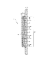
- FIG. 1 is a cross-sectional view showing a cross section in the light emitting region of the organic EL display device according to the first embodiment of the present invention.
- FIG. 2 is a cross-sectional view showing a cross section in a non-light emitting region of the organic EL display device.
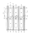
- FIG. 3 is an enlarged plan view for explaining the main configuration of the organic EL display device.
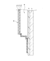
- FIG. 4 is an enlarged cross-sectional view for explaining a specific configuration example of the sealing film shown in FIG.
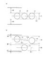
- FIG. 5 is a view for explaining an anchor effect on the sealing film by the protrusion shown in FIG.
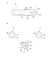
- FIG. 6A is a diagram illustrating the anchor effect according to Comparative Example 1
- FIG. 6B is a diagram illustrating the anchor effect according to the present embodiment product.
- FIG. 7 (a) is a figure explaining the anchor effect by the comparative example 2
- FIG.7 (b) is a figure explaining the anchor effect by this embodiment goods.
- FIG. 8 is a cross-sectional view showing a cross section in the light emitting region of the organic EL display device according to the second embodiment of the present invention.
- FIG. 9 is a cross-sectional view showing a cross section in a non-light emitting region of the organic EL display device shown in FIG.
- FIG. 10 is a cross-sectional view showing a cross section in the light emitting region of the organic EL display device according to the third embodiment of the present invention.
- FIG. 8 is a cross-sectional view showing a cross section in the light emitting region of the organic EL display device according to the second embodiment of the present invention.
- FIG. 9 is a cross-sectional view showing a cross section in a non-light emitting region of the organic EL display device shown in FIG.
- FIG. 10 is a cross-sectional view showing
- FIG. 11 is a cross-sectional view showing a cross section in a non-light-emitting region of the organic EL display device shown in FIG. 12A and 12B are a perspective view and a side view, respectively, of a display device including an organic EL display device according to the fourth embodiment of the present invention.
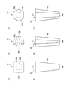
- FIG. 13 is an enlarged plan view for explaining a main configuration of the organic EL display device at the boundary portions F1 and F2 shown in FIG. 14 (a) and 14 (b) are a plan view and a side view, respectively, of Modification 1 of the projection, and FIGS. 14 (c) and 14 (d) are modifications of the projection, respectively.
- Fig. 14 (e) and Fig. 14 (f) are a plan view and a side view, respectively, of Modification 3 of the protrusion.
- FIG. 1 is a cross-sectional view showing a cross section in the light emitting region of the organic EL display device according to the first embodiment of the present invention.
- FIG. 2 is a cross-sectional view showing a cross section in a non-light emitting region of the organic EL display device.
- an organic EL display device 1 according to the present embodiment includes a TFT substrate 2 as a substrate and an organic EL element 4 as an electroluminescence element provided on the TFT substrate 2.
- the organic EL element 4 forms a rectangular pixel area PA having a plurality of pixels (including a plurality of subpixels). Sealed by the sealing film 14.
- the pixel area PA constitutes the display unit of the organic EL display device 1 and displays information. That is, in this pixel area PA, as will be described in detail later, a plurality of pixels (a plurality of subpixels) are arranged in a matrix, and the organic EL element 4 emits light for each subpixel, thereby displaying information. Is configured to do.
- the TFT substrate 2 is made of, for example, a glass material.
- the TFT substrate 2 is provided with a base film (insulating film) 6 so as to cover the entire surface thereof.
- a TFT (thin film transistor) 7 is provided on the base film 6 for each subpixel of the pixel region PA.
- wirings 8 including a plurality of source lines (signal lines) and a plurality of gate lines provided in a matrix are formed.
- a source driver and a gate driver are respectively connected to the source line and the gate line (not shown), and the TFT 7 for each sub-pixel is driven in accordance with an image signal input from the outside.
- the TFT 7 functions as a switching element that controls light emission of the corresponding sub-pixel, and any one of red (R), green (G), and blue (B) formed by the organic EL element 4 is used. The light emission in the color sub-pixel is controlled.
- the base film 6 is for preventing the characteristics of the TFT 7 from deteriorating due to impurity diffusion from the TFT substrate 2 to the TFT 7. If there is no concern about such deterioration, the base film 6 may be omitted. it can.
- an interlayer insulating film 9, an edge cover 10, and a first electrode 11 of the organic EL element 4 are formed on the TFT substrate 2.
- the interlayer insulating film 9 also functions as a planarizing film, and is provided on the base film 6 so as to cover the TFT 7 and the wiring 8.
- the edge cover 10 is formed on the interlayer insulating film 9 so as to cover the pattern end of the first electrode 11.
- the edge cover 10 also functions as an insulating layer for preventing a short circuit between the first electrode 11 and a second electrode 13 described later.
- the first electrode 11 is connected to the TFT 7 through a contact hole formed in the interlayer insulating film 9.
- the opening of the edge cover 10, that is, the portion where the first electrode 11 is exposed substantially constitutes the light emitting region of the organic EL element 4, and emits one of RGB color lights as described above.
- the organic EL display device 1 of the present embodiment is configured so that full color display can be performed.
- the organic EL display device 1 of the present embodiment constitutes an active matrix display device having TFTs (thin film transistors) 7.
- an organic EL layer 12 and a second electrode 13 are formed on the first electrode 11, and the first electrode 11, the organic EL layer 12, and the second electrode 13
- the organic EL element 4 is configured. That is, the organic EL element 4 is a light emitting element that can emit light with high luminance by, for example, low-voltage direct current driving, and includes a first electrode 11, an organic EL layer 12, and a second electrode 13.
- the organic EL layer 12 when the first electrode 11 is an anode, the organic EL layer 12 includes a hole injection layer, a hole transport layer, a light emitting layer, an electron transport layer, an electron injection layer, and the like from the first electrode 11 side. Laminated (not shown), and further, a second electrode 13 as a cathode is formed. In addition to this description, a single layer may have two or more functions such as a hole injection layer / hole transport layer. In the organic EL layer 12, a carrier blocking layer or the like may be appropriately inserted.
- the layer order in the organic EL layer 12 is reversed from the above.
- the organic EL display device 1 is a bottom emission type in which light is emitted from the TFT substrate 2 side. . That is, in the bottom emission type organic EL display device 1, the surface of the first electrode 11 on the TFT substrate 2 side constitutes a substantial light emitting surface of the organic EL element 4, and emits light to the outside. ing.
- the organic EL display device 1 is a top emission type that emits light from the sealing film 14. Become. That is, in the top emission type organic EL display device 1, the surface of the first electrode 11 on the sealing film 14 side constitutes a substantial light emitting surface of the organic EL element 4 so that light is emitted to the outside. It has become.
- the organic EL element 4 is sealed by the sealing film 14, and moisture, oxygen, and the like permeate (infiltrate) from the outside by the sealing film 14. ) To prevent the organic EL element 4 from deteriorating.
- the base film 6 and the organic EL element 4 are sequentially provided on the TFT substrate 2 in the non-light emitting region of the organic EL display device 1.
- the non-light emitting region only the signal line 8, the interlayer insulating film 9, the edge cover 10, the organic EL layer 12, and the second electrode 13 among the organic EL elements 4 are provided.
- a plurality of protrusions 15 are provided for each subpixel in an island shape to prevent the sealing film 14 from peeling off (details will be described later).
- FIG. 3 is an enlarged plan view for explaining the main configuration of the organic EL display device.
- 1 and 2 are a cross-sectional view taken along the line II and a line II-II of FIG. 3, respectively.
- each of the plurality of subpixels P is partitioned by two signal lines 8 and a gate line 8 g connected to the gate of the TFT 7.
- the dimensions in the left-right direction in FIG. 3 are the center lines of the two signal lines 8 arranged close to each other and the two signal lines 8 arranged close to each other.
- the vertical dimension in FIG. 3 is the dimension between the centers of the two gate lines 8g adjacent to each other (shown as “L2” in FIG. 3).
- the area of the pixel region is defined by the horizontal dimension and the vertical dimension in FIG.
- one set of red, green, and blue subpixels Pr, Pg, and Pb constitutes one pixel.
- a portion exposed from the opening re of the edge cover 10 constitutes a substantial light emitting region of the red subpixel Pr.
- a portion exposed from the opening ge of the edge cover 10 constitutes a substantial light emitting region of the green subpixel Pg, and in the blue subpixel Pb, the opening of the edge cover 10 is formed.
- each protrusion 15 is provided for each subpixel P in the non-light emitting region between two subpixels P adjacent in the vertical direction in FIG. 3. These protrusions 15 are included in a prevention portion for preventing the peeling of the sealing film 14 and are disposed only in the non-light emitting region.
- Each protrusion 15 has, for example, a cylindrical shape, and is covered with the sealing film 14 and has a shape protruding from the organic EL element 4 side toward the sealing film 14 side, as shown in FIG. Yes.
- each protrusion 15 is configured to have a circular upper surface 15a that contacts the organic EL layer 12, a circular lower surface 15b that contacts the edge cover 10 and is concentric with the upper surface 15a.
- the light-emitting surface of the organic EL element 4 is configured in an inversely tapered shape having an inclined surface 15c having an obtuse angle. And each protrusion 15 can prevent the film peeling of the said sealing film 14 by acting the anchor effect with respect to the sealing film 14 by the inclined surface 15c (it mentions later for details).
- each projection 15 is set to have a height from the edge cover 10 of, for example, 5 to 10 ⁇ m.
- the projection is formed on the edge cover 10 by, for example, photolithography.
- the three projections 15 provided for each sub-pixel P have an area ratio Sr of the inclined surface 15c obtained in (1) below of 3% or more. It is configured as such. Thereby, it can prevent reliably that the said anchor effect by the protrusion 15 falls, and generation
- Sr (S1-S2) / S3 ⁇ (1)
- S1 is the total surface area of the three protrusions 15 on the sealing film 14 side, that is, the upper surface 15a
- S2 is the surface of the three protrusions 15 on the organic EL element 4 side, that is, the lower surface 15b
- S3 is the area of the pixel region of the sub-pixel P (that is, the horizontal dimension in FIG. 3 (shown by “L1” in FIG. 3) and the vertical dimension (“L2 in FIG. 3)”. ”)").
- the area ratio Sr can be appropriately adjusted depending on the height dimension (film thickness) of the protrusions 15, the inclination angle (taper angle) of the inclined surface 15c, the size, the number, and the like.
- the tilt angle is set to a value (obtuse angle) within a range of, for example, 100 degrees to 150 degrees with respect to the light emitting surface of the organic EL element 4.
- the three projections 15 are arranged on the same straight line at the respective centers. (The details will be described later.)
- FIG. 4 is an enlarged sectional view for explaining a specific configuration example of the sealing film shown in FIG.
- the sealing film 14 uses a laminated structure of an inorganic layer and an organic layer, and prevents the penetration (penetration) of moisture and oxygen into the organic EL element 4 from the outside as much as possible.
- the element 4 is prevented from being deteriorated as much as possible.
- a first inorganic layer 14 a, an organic layer 14 b, and a second inorganic layer 14 c are provided so as to sequentially cover the organic EL element 4. ing.
- the first inorganic layer 14a, the organic layer 14b, and the second inorganic layer 14c are formed using, for example, a CVD method, a sputtering method, an ALD (Atomic Layer Deposition) method, or the like.
- silicon nitride, silicon oxide, silicon oxynitride, or aluminum oxide is used for the first and second inorganic layers 14a and 14c.
- the organic layer 14b is made of silicon oxide carbide, acrylate, polyurea, parylene, polyimide, polyamide, or the like.
- the sealing film 14 has a total film thickness of 2 ⁇ m or more. Thereby, the sealing film 14 can seal the organic EL element 4 reliably. Further, in the sealing film 14, the thickness of the first inorganic layer 14 a is smaller than the height of the protrusion 15. Thereby, when forming the 1st inorganic layer 14a after installing the protrusion 15, it can prevent that a space
- the first inorganic layer 14a when the film thickness of the first inorganic layer 14a is higher than the height of the protrusion 15, the first inorganic layer 14a naturally forms a slope with the inclined surface 15c of the protrusion 15 due to the film stress of the first inorganic film 14a. Air gaps are likely to occur between them. Furthermore, since the reverse taper shape of the protrusion 15 is filled with the first inorganic layer 14a and becomes gentle, the anchor effect is less likely to act on the organic layer 14b and the second inorganic layer 14c.
- FIG. 5 is a diagram for explaining an anchor effect on the sealing film by the protrusion shown in FIG.
- FIG. 6A is a diagram illustrating the anchor effect according to Comparative Example 1
- FIG. 6B is a diagram illustrating the anchor effect according to the present embodiment product.
- the peeling force is applied to the protrusion 15 and the sealing film 14 by the arrow B in FIG. And C as a deformation force.
- the protrusion 15 and the sealing film 14 can prevent peeling of the sealing film 14 by withstanding the corresponding deformation force due to its rigidity. That is, in the organic EL display device 1 of the present embodiment, the protrusion 15 and the sealing film 14 receive the corresponding deformation force by rigidity, thereby increasing the film stress associated with the thickening of the sealing film 14.
- one protrusion 25 as a prevention portion can be provided for each sub-pixel P. That is, the protrusion 25 has an upper surface 25 a that contacts the organic EL layer 12, a circular lower surface 25 b that contacts the edge cover 10, and an inclined surface 25 c that forms an obtuse angle with respect to the light emitting surface of the organic EL element 4. It has a reverse tapered shape. Even when such a protrusion 25 is used, it is possible to prevent the sealing film 14 from peeling off, but a plurality of, for example, three, as in the present embodiment product shown in FIG.
- the deformation force in each direction of the protrusions (preventing portions) 15 can be easily made uniform, and the area ratio Sr of the inclined surface 15c in each protrusion 15 can be increased. It is preferable in that it can be improved and the resistance against the peeling force, that is, the anchor effect of the prevention portion can be improved.
- the protrusion 25 shown in FIG. 6A is installed for each sub-pixel P, the shape thereof is unsatisfactory in each direction within the light emitting surface (that is, the vertical direction and the horizontal direction in FIG. 6A). Since it is uniform, the resistance to the peeling force in each of the above directions becomes non-uniform. That is, of the peeling force applied obliquely to the light emitting surface, the force parallel to the pixel surface is divided into a deformation force perpendicular to the inclined surface 25c of the protrusion 25 and a parallel shearing force. Therefore, on the inclined surface 25c of the side (short side) parallel to the vertical direction in FIG.
- the shearing force Ea1 and the deformation force Da1 work, but since the area of the inclined surface 25c is small on this short side, Resistance to the deformation force Da1 is reduced.
- the shearing force Eb1 and the deformation force Db1 act, but on this long side, the area of the inclined surface 25c is the short side. Since it is larger, the resistance to the deformation force Db1 is increased. As a result, when the protrusion 25 is used, the resistance to the peeling force becomes uneven due to the vertical direction and the horizontal direction in FIG.
- the area ratio Sr of the inclined surface 15c of each protrusion 15 can also be improved, and the tolerance to peeling force can also be improved.
- the cylindrical projection 15 is used, the same resistance to peeling force (anchor effect) can be obtained in any direction of the light emitting surface.
- FIG. 7 (a) is a diagram for explaining the anchor effect according to Comparative Example 2
- FIG. 7 (b) is a diagram for explaining the anchor effect according to this embodiment product.
- the centers of the three protrusions 15 ' are arranged on the straight line CL1.
- the width indicated by “H1” in FIG. 7A that is, the projection 15.
- Resistance to the peeling force occurs only in the portion within the range of 'diameter'.
- the protrusion 15 ′ is not provided, and thus resistance to the peeling force does not occur. Therefore, there is an increased possibility that the sealing film 14 is peeled off from the portion where the protrusion 15 ′ is not present.
- the three protrusions 15 are installed such that their centers are not arranged on the same straight line. That is, the center of the protrusion 15 on the left side of FIG. 7B is arranged on the straight line CL2. Further, the center projection 15 of FIG. 7B is arranged on the straight line CL3, and the right projection 15 of FIG. 7B has the center arranged on the straight line CL4.
- the portion within the width range indicated by “H4” in FIG. 7B and the portion within the width range indicated by “H5” in FIG. Resistance (anchor effect) can be produced. Further, in the present embodiment, as shown by the widths “H6” and “H7” in FIG. 7B, resistance to peeling force does not occur as compared with Comparative Example 2 shown in FIG. 7A. The area can be reduced.
- the sealing film 14 is peeled off by the three protrusions 15.
- the prevention function can be improved, and the occurrence of film peeling of the sealing film 14 can be more reliably prevented.
- the organic EL display device 1 of the present embodiment configured as described above, only the non-light emitting region of the organic EL element (electroluminescence element) 4 is inclined with an obtuse angle with respect to the light emitting surface of the organic EL element 4.
- a protrusion (prevention unit) 15 that has a surface 15 c and prevents the sealing film 14 from peeling off is provided.
- an organic EL display device (electroluminescence device) 1 that can prevent the peeling of the sealing film 14 can be configured.
- the sealing function of the organic EL element 4 by the sealing film 14 can be maintained for a long time, and high reliability in which the occurrence of deterioration of the organic EL element 4 is more reliably suppressed.
- the organic EL display device 1 having the above can be easily configured.
- the prevention portion includes a plurality of protrusions 15 that are covered with the sealing film 14 and protrude from the organic EL element 4 side toward the sealing film 14 side.
- the plurality of protrusions 15 can reliably prevent the peeling of the sealing film 14.
- the occurrence of film peeling of the sealing film 14 can be prevented more reliably.
- FIG. 8 is a cross-sectional view showing a cross section in the light emitting region of the organic EL display device according to the second embodiment of the present invention.
- FIG. 9 is a cross-sectional view showing a cross section in a non-light emitting region of the organic EL display device shown in FIG.
- an organic EL element is formed by a counter substrate facing the TFT substrate and a sealing material provided between the TFT substrate and the counter substrate. It is a sealed point.
- symbol is attached
- the organic EL display device 1 of the present embodiment includes a counter substrate 3 facing the TFT substrate 2, and a sealing material 5 provided between the TFT substrate 2 and the counter substrate 3.
- the organic EL element 4 is enclosed by a TFT substrate 2, a counter substrate 3, and a sealing material 5.
- the organic EL display device 1 of the present embodiment includes the counter substrate 3 so as to face the organic EL element 4 and the filler 16 filled in the space between the TFT substrate 2, the counter substrate 3, and the sealing material 5.
- a color filter 17 is provided on the top.
- the organic EL display device 1 unlike the first embodiment, after the sealing film 14 is formed, the pixel region PA is surrounded by the sealing material 5 and the filler 16 is injected. Then, the counter substrate 3 provided with the color filter 17 is bonded.
- the organic EL element 4 by encapsulating the organic EL element 4 with the structure as described above, it is possible to suppress deterioration of the organic EL element 4 due to moisture or oxygen entering the organic EL element 4 from the outside.
- the reliability of the organic EL display device 1 can be improved. In the present embodiment, since the reliability can be ensured by the simple sealing film 14, the cost of the sealing film forming process can be reduced.
- a glass material is used for the counter substrate 3 in the same manner as the TFT substrate 2.
- a low moisture permeability material is used for the sealing material 5.
- the filler 16 for example, a material having low moisture permeability or a material containing a desiccant or an oxygen absorbing material is used.
- the filler 16 may be a curable type or a non-curable type. In the case of the non-curable type, the filler 16 exists between the TFT substrate 2 and the counter substrate 3 in a liquid state.
- the color filter 17 has a function of modulating light emitted from the organic EL element. Specifically, for example, when the organic EL element 4 emits white light, the color filter 17 has a red sub-pixel corresponding to the red, green, and blue color filter portions provided in the color filter 17. In Pr, the green subpixel Pg, and the blue subpixel Pb, the white light from the organic EL element 4 is modulated into red light, green light, and blue light, respectively.
- the organic EL element 4 when the organic EL element 4 emits red light, green light, and blue light at the red subpixel Pr, the green subpixel Pg, and the blue subpixel Pb, respectively, By modulating the light through the red, green, and blue color filter sections, it is possible to improve the color purity of each color and to suppress the color shift when the viewing angle changes.
- the installation of the color filter 17 can be omitted.
- the color filter 17 and the TFT substrate 2 are provided on the color filter 17 on the side of the organic EL element 4 on the TFT substrate 2 and the red, green, and blue color filter portions provided on the color filter 17.
- the TFT substrate 2 and the counter substrate 3 are bonded together.
- the present embodiment can achieve the same operations and effects as the first embodiment. Moreover, in this embodiment, since the organic EL element 4 is enclosed by the TFT substrate 2, the counter substrate 3, and the sealing material 5, it is possible to further suppress the intrusion of moisture and oxygen from the outside. Degradation of the organic EL element 4 due to can be further suppressed.
- the filler 16 since the filler 16 is present on the sealing film 14, the difference in thermal expansion coefficient between the sealing film 14 and the filler 16, and curing shrinkage (a curable filler is used).
- the stress is applied to the sealing film 14. This stress is also weak in film adhesion between the first electrode 11 and the organic EL layer 12, between each layer in the organic EL layer, between the second electrode 13 and the organic EL layer 12 and the sealing film 14. It acts on the part (interface) and causes the peeling of the sealing film 14.
- three protrusions (prevention portions) 15 are provided for each sub-pixel, as in the first embodiment (see FIG. 9). 14, the anchor effect by the protrusion 15 can be effectively exerted, and the peeling of the sealing film 14 can be prevented.
- a highly reliable organic EL display device 1 can be configured as in the case of the first embodiment.
- FIG. 10 is a cross-sectional view showing a cross section in the light emitting region of the organic EL display device according to the third embodiment of the present invention.
- FIG. 11 is a cross-sectional view showing a cross section in a non-light-emitting region of the organic EL display device shown in FIG.
- the main difference between this embodiment and the second embodiment is that a flexible substrate is used for the TFT substrate and the counter substrate.
- symbol is attached
- a flexible substrate having flexibility (flexibility), for example, a material such as a film is used as the TFT substrate 2 ′ and the counter substrate 3 ′. ing.
- the counter substrate 3 ′ is bonded with the adhesive 18.
- the organic EL display device 1 having flexibility (flexibility) can be configured in the present embodiment.
- the color of the light emitted from the organic EL element 4 is modulated on the surface of the counter substrate 3 ′ on the TFT substrate 2 ′ side in the same manner as in the second embodiment.
- a filter may be provided.
- the TFT substrate 2 ′ and the counter substrate 3 ′ are aligned in units of RGB subpixels Pr, Pg, and Pb, and then the adhesive 18 is used. Pasted together.
- the surface of the counter substrate 3 ′ on the TFT substrate 2 ′ side may be provided so as to cover a gas barrier film in which, for example, silicon nitride or silicon oxynitride is laminated.
- a gas barrier film in which, for example, silicon nitride or silicon oxynitride is laminated.
- the amount of moisture and oxygen entering the organic EL element 4 from the outside through the counter substrate 3 ′ can be reduced.
- deterioration of the organic EL element 4 can be suppressed, and the reliability of the organic EL display device 1 can be improved.
- the reliability can be ensured by the simple sealing film 14, the cost of the sealing film forming process can be reduced.
- a sealing material surrounding the pixel area PA may be formed.
- a low moisture-permeable sealing material it is possible to reduce moisture and oxygen that enter from the outside to the ends of the bonded TFT substrate 2 ′ and counter substrate 3 ′. Thereby, it can suppress that the organic EL element 4 deteriorates, and can improve the reliability of the organic EL display apparatus 1.
- the present embodiment can achieve the same operations and effects as those of the second embodiment.
- the flexible substrate is used for the TFT substrate 2 ′ and the counter substrate 3 ′, the organic EL display device 1 having flexibility (flexibility) can be configured.
- a highly reliable organic EL display device 1 can be configured as in the case of the first embodiment.
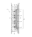
- FIG. 12A and 12B are a perspective view and a side view, respectively, of a display device including an organic EL display device according to the fourth embodiment of the present invention.
- FIG. 13 is an enlarged plan view for explaining a main configuration of the organic EL display device at the boundary portions F1 and F2 shown in FIG.
- the present embodiment includes a reference light emitting surface and an inclined light emitting surface that is continuously provided on an end surface of the reference light emitting surface and is inclined with respect to the reference light emitting surface.
- the installation density of protrusions at the boundary between the reference light emitting surface and the inclined light emitting surface is the installation density of protrusions at portions other than the boundary portion of the reference light emitting surface, and the protrusion at portions other than the boundary portion of the inclined light emitting surface. This is a point that is larger than the installation density of objects.
- symbol is attached
- the organic EL display device 1 of the present embodiment is continuous to the reference light emitting surface DP1 and the end surface of the reference light emitting surface DP1, for example, the left and right short sides. And provided with inclined light emitting surfaces DP2 and DP3 inclined with respect to the reference light emitting surface DP1.
- the reference organic light emitting surface DP1 and the inclined light emitting surfaces DP2 and DP3 are provided by bending both ends of the flexible organic EL display device 1 of the third embodiment and attaching them to the housing 19.
- An organic EL display device 1 is configured. Further, in the organic EL display device 1 of the present embodiment, as illustrated by a two-dot chain line in FIG. 12A, one character “one” is formed by the reference light emitting surface DP1 and the inclined light emitting surfaces DP2 and DP3. It can be displayed.
- the boundary between the reference light emitting surface DP1 and the inclined light emitting surface DP2 (shown as “F1” in FIGS. 12A and 12B), and the reference light emitting surface DP1 and the inclined light emitting surface.
- the protrusion 15 is disposed at a portion other than the boundary portion of the reference light emitting surface DP1.
- each of the above-described boundary portions F1 and F2 four protrusions 15 are provided for each sub-pixel P as illustrated in FIG.
- the sealing film 14 is provided. Occurrence of film peeling can be prevented.
- the present embodiment can achieve the same operations and effects as the third embodiment.
- an inclined light emitting surface may be provided not only on the short side of the reference light emitting surface DP1, but also on the long side.
- an organic EL element is used as an electroluminescence element.
- the present invention is not limited to this, and for example, an inorganic EL element having an inorganic compound may be used.
- the present invention is applied to an active matrix type organic EL display device having a TFT (thin film transistor) 7 .
- TFT thin film transistor
- the present invention is not limited to this, and a passive device without a thin film transistor is provided.
- the present invention can also be applied to a matrix type organic EL display device.
- the present invention is not limited to this, and can be applied to an illumination device such as a backlight device.
- the prevention unit of the present invention is a non-light-emitting region of the electroluminescence element.
- the prevention unit of the present invention has an inclined surface with an obtuse angle with respect to the light emitting surface of the electroluminescent element and prevents peeling of the sealing film.
- one or more stripe-shaped protrusions may be provided for each subpixel.
- the case where a plurality of protrusions are provided for each sub-pixel is preferable in that the occurrence of peeling of the sealing film can be more reliably prevented. .
- a configuration using a prismatic protrusion 35 having an inclined surface 35c having an obtuse angle may be used.
- the design is simple, so that the projection 35 can be easily formed.
- a configuration using a cross columnar projection 45 having an inclined surface 45c having an obtuse angle may be used.
- the length of the inclined surface 45c can be increased within the same area, and the anchor effect can be easily improved.
- a configuration using a hexagonal columnar projection 55 having an inclined surface 45c having an obtuse angle may be used. Further, when such a hexagonal columnar projection 55 is used, a close-packed structure can be easily obtained, and the exclusive area ratio of the projection 55 can be easily increased.
- the protrusion as the prevention portion is provided in the non-light-emitting region between the two sub-pixels P adjacent in the vertical direction in FIG. 3 .
- the present invention is not limited to this, and a non-light emitting area between two subpixels P adjacent in the left-right direction in FIG. 3 or a non-light emitting area outside the pixel area may be used.
- the present invention is useful for an electroluminescence device that can prevent the peeling of the sealing film.
- Organic EL display device 2 2 'TFT substrate (substrate) 3, 3 'Counter substrate 4 Organic EL element (electroluminescence element) 5 Sealant 14 Sealing Film 14a First Inorganic Layer 14b Organic Layer 14c Second Inorganic Layer 15, 25, 35, 45, 55 Protrusion (Prevention Section) 15c, 25c, 35c, 45c, 55c Inclined surface P, Pr, Pg, Pb Sub-pixel DP1 Reference light emitting surface DP2, DP3 Inclined light emitting surface
Landscapes
- Physics & Mathematics (AREA)
- Optics & Photonics (AREA)
- Engineering & Computer Science (AREA)
- Microelectronics & Electronic Packaging (AREA)
- Electroluminescent Light Sources (AREA)
Abstract
Description
前記エレクトロルミネッセンス素子を封止する封止膜を備え、
前記エレクトロルミネッセンス素子の発光面に対して、鈍角となる傾斜面を有し、かつ、前記封止膜の膜剥がれを防止する防止部を前記エレクトロルミネッセンス素子の非発光領域のみに設けたことを特徴とするものである。
Sr = (S1-S2)/S3 ―――(1)
3%以上となるように、前記副画素毎の複数の前記突起物が設けられていることが好ましい。
前記防止部では、前記基準発光面と前記傾斜発光面との境界部分での前記突起物の設置密度が、前記基準発光面の前記境界部分以外の部分での前記突起物の設置密度、及び前記傾斜発光面の前記境界部分以外の部分での前記突起物の設置密度よりも大きい値とされていることが好ましい。
前記エレクトロルミネッセンス素子は、前記基板、前記対向基板、及び前記シール材によって封入されてもよい。
図1は、本発明の第1の実施形態にかかる有機EL表示装置の発光領域での断面を示す断面図である。図2は、上記有機EL表示装置の非発光領域での断面を示す断面図である。図1において、本実施形態の有機EL表示装置1は、基板としてのTFT基板2、及びこのTFT基板2上に設けられたエレクトロルミネッセンス(Electro Luminescence)素子としての有機EL素子4を備えている。
ここで、S1は3個の突起物15の封止膜14側の表面、つまり上面15aの面積の総和であり、S2は3個の突起物15の有機EL素子4側の表面、つまり下面15bの面積の総和であり、S3は副画素Pの画素領域の面積(つまり、上記図3の左右方向の寸法(図3に“L1”にて図示)と上下方向の寸法(図3に“L2”にて図示)の積)である。また、この面積率Srは、突起物15の高さ寸法(膜厚)、傾斜面15cの傾斜角(テーパ角)、サイズ、個数などにより適宜調整することができる。
図8は、本発明の第2の実施形態にかかる有機EL表示装置の発光領域での断面を示す断面図である。図9は、図8に示した有機EL表示装置の非発光領域での断面を示す断面図である。
図10は、本発明の第3の実施形態にかかる有機EL表示装置の発光領域での断面を示す断面図である。図11は、図10に示した有機EL表示装置の非発光領域での断面を示す断面図である。
図12(a)及び図12(b)は、それぞれ本発明の第4の実施形態にかかる有機EL表示装置を含んだ表示装置の斜視図及び側面図である。図13は、図12(a)に示した境界部分F1及びF2での有機EL表示装置の要部構成を説明する拡大平面図である。
2、2' TFT基板(基板)
3、3' 対向基板
4 有機EL素子(エレクトロルミネッセンス素子)
5 シール材
14 封止膜
14a 第1の無機層
14b 有機層
14c 第2の無機層
15、25、35、45、55 突起物(防止部)
15c、25c、35c、45c、55c 傾斜面
P、Pr、Pg、Pb 副画素
DP1 基準発光面
DP2、DP3 傾斜発光面
Claims (10)
- 基板と、前記基板上に設けられたエレクトロルミネッセンス素子を備えたエレクトロルミネッセンス装置であって、
前記エレクトロルミネッセンス素子を封止する封止膜を備え、
前記エレクトロルミネッセンス素子の発光面に対して、鈍角となる傾斜面を有し、かつ、前記封止膜の膜剥がれを防止する防止部を前記エレクトロルミネッセンス素子の非発光領域のみに設けた、
ことを特徴とするエレクトロルミネッセンス装置。 - 前記防止部には、前記封止膜に覆われるとともに、前記エレクトロルミネッセンス素子側から前記封止膜側に向かって突起した複数の突起物が含まれている請求項1に記載のエレクトロルミネッセンス装置。
- 前記防止部では、前記エレクトロルミネッセンス素子に設けられた副画素毎に、前記突起物が複数設置されている請求項2に記載のエレクトロルミネッセンス装置。
- 前記防止部では、前記突起物の前記封止膜側の表面の面積をS1とし、前記突起物の前記エレクトロルミネッセンス素子側の表面の面積をS2とし、前記副画素の面積をS3としたときに、下記(1)式で求められる前記傾斜面の面積率Srが、
Sr = (S1-S2)/S3 ―――(1)
3%以上となるように、前記副画素毎の複数の前記突起物が設けられている請求項3に記載のエレクトロルミネッセンス装置。 - 前記防止部では、3個以上の前記突起物が前記副画素毎に設けられた場合、これら3個以上の前記突起物は、その各中心が同一の直線上に配置されないように設置されている請求項3または4に記載のエレクトロルミネッセンス装置。
- 前記エレクトロルミネッセンス素子では、その発光面が基準発光面と、前記基準発光面の端面に連続的に設けられるとともに、当該基準発光面に対して傾斜した傾斜発光面とを有するように構成され、
前記防止部では、前記基準発光面と前記傾斜発光面との境界部分での前記突起物の設置密度が、前記基準発光面の前記境界部分以外の部分での前記突起物の設置密度、及び前記傾斜発光面の前記境界部分以外の部分での前記突起物の設置密度よりも大きい値とされている請求項2~5のいずれか1項に記載のエレクトロルミネッセンス装置。 - 前記基板に対向する対向基板と、前記基板と前記対向基板との間に設けられたシール材を備え、
前記エレクトロルミネッセンス素子は、前記基板、前記対向基板、及び前記シール材によって封入されている請求項1~6のいずれか1項に記載のエレクトロルミネッセンス装置。 - 前記基板及び前記対向基板には、フレキシブル基板が用いられている請求項7に記載のエレクトロルミネッセンス装置。
- 前記封止膜は、無機層と有機層との積層によって構成されている請求項1~8のいずれか1項に記載のエレクトロルミネッセンス装置。
- 前記封止膜では、その膜厚が2μm以上とされている請求項1~9のいずれか1項に記載のエレクトロルミネッセンス装置。
Priority Applications (3)
| Application Number | Priority Date | Filing Date | Title |
|---|---|---|---|
| JP2015560976A JP5992641B2 (ja) | 2014-02-10 | 2015-02-03 | エレクトロルミネッセンス装置 |
| CN201580007967.5A CN106063374B (zh) | 2014-02-10 | 2015-02-03 | 电致发光装置 |
| US15/112,226 US9653702B2 (en) | 2014-02-10 | 2015-02-03 | Electroluminescent device |
Applications Claiming Priority (2)
| Application Number | Priority Date | Filing Date | Title |
|---|---|---|---|
| JP2014-023491 | 2014-02-10 | ||
| JP2014023491 | 2014-02-10 |
Publications (1)
| Publication Number | Publication Date |
|---|---|
| WO2015119086A1 true WO2015119086A1 (ja) | 2015-08-13 |
Family
ID=53777891
Family Applications (1)
| Application Number | Title | Priority Date | Filing Date |
|---|---|---|---|
| PCT/JP2015/052897 Ceased WO2015119086A1 (ja) | 2014-02-10 | 2015-02-03 | エレクトロルミネッセンス装置 |
Country Status (4)
| Country | Link |
|---|---|
| US (1) | US9653702B2 (ja) |
| JP (1) | JP5992641B2 (ja) |
| CN (1) | CN106063374B (ja) |
| WO (1) | WO2015119086A1 (ja) |
Cited By (2)
| Publication number | Priority date | Publication date | Assignee | Title |
|---|---|---|---|---|
| WO2017068103A1 (fr) * | 2015-10-23 | 2017-04-27 | Commissariat A L'energie Atomique Et Aux Energies Alternatives | Dispositif electronique organique a microstructures |
| GB2627852A (en) * | 2022-12-30 | 2024-09-04 | Lg Display Co Ltd | Display device |
Families Citing this family (1)
| Publication number | Priority date | Publication date | Assignee | Title |
|---|---|---|---|---|
| CN106935728B (zh) | 2017-03-22 | 2019-06-28 | 京东方科技集团股份有限公司 | Oled封装结构、显示面板以及制备封装结构的方法 |
Citations (4)
| Publication number | Priority date | Publication date | Assignee | Title |
|---|---|---|---|---|
| JP2000100577A (ja) * | 1998-09-25 | 2000-04-07 | Sony Corp | 光学的素子及びその製造方法 |
| JP2004288403A (ja) * | 2003-03-19 | 2004-10-14 | Optrex Corp | 有機elディスプレイの製造方法および有機elディスプレイ |
| JP2006172940A (ja) * | 2004-12-16 | 2006-06-29 | Toshiba Matsushita Display Technology Co Ltd | 表示装置及び表示装置の製造方法 |
| JP2010199095A (ja) * | 2008-06-25 | 2010-09-09 | Sony Corp | ドナー基板および表示装置の製造方法 |
Family Cites Families (8)
| Publication number | Priority date | Publication date | Assignee | Title |
|---|---|---|---|---|
| US5952037A (en) * | 1995-03-13 | 1999-09-14 | Pioneer Electronic Corporation | Organic electroluminescent display panel and method for manufacturing the same |
| JP4990801B2 (ja) | 2006-01-31 | 2012-08-01 | エルジー ディスプレイ カンパニー リミテッド | El装置 |
| JP2009037812A (ja) | 2007-07-31 | 2009-02-19 | Sumitomo Chemical Co Ltd | 有機el装置およびその製造方法 |
| CN101765871B (zh) * | 2007-12-06 | 2011-06-15 | 夏普株式会社 | 显示装置 |
| JP2013077382A (ja) | 2011-09-29 | 2013-04-25 | Canon Inc | 電界発光表示装置 |
| JP5967982B2 (ja) * | 2012-03-07 | 2016-08-10 | 東レエンジニアリング株式会社 | プラズマcvd法により形成された化学蒸着膜 |
| CN104396344A (zh) * | 2012-10-29 | 2015-03-04 | 日东电工株式会社 | 使用了卷对卷方式的有机电致发光面板的制造方法 |
| KR102117890B1 (ko) * | 2012-12-28 | 2020-06-02 | 엘지디스플레이 주식회사 | 플렉서블 표시 장치 및 플렉서블 표시 장치 제조 방법 |
-
2015
- 2015-02-03 CN CN201580007967.5A patent/CN106063374B/zh active Active
- 2015-02-03 WO PCT/JP2015/052897 patent/WO2015119086A1/ja not_active Ceased
- 2015-02-03 US US15/112,226 patent/US9653702B2/en active Active
- 2015-02-03 JP JP2015560976A patent/JP5992641B2/ja active Active
Patent Citations (4)
| Publication number | Priority date | Publication date | Assignee | Title |
|---|---|---|---|---|
| JP2000100577A (ja) * | 1998-09-25 | 2000-04-07 | Sony Corp | 光学的素子及びその製造方法 |
| JP2004288403A (ja) * | 2003-03-19 | 2004-10-14 | Optrex Corp | 有機elディスプレイの製造方法および有機elディスプレイ |
| JP2006172940A (ja) * | 2004-12-16 | 2006-06-29 | Toshiba Matsushita Display Technology Co Ltd | 表示装置及び表示装置の製造方法 |
| JP2010199095A (ja) * | 2008-06-25 | 2010-09-09 | Sony Corp | ドナー基板および表示装置の製造方法 |
Cited By (3)
| Publication number | Priority date | Publication date | Assignee | Title |
|---|---|---|---|---|
| WO2017068103A1 (fr) * | 2015-10-23 | 2017-04-27 | Commissariat A L'energie Atomique Et Aux Energies Alternatives | Dispositif electronique organique a microstructures |
| FR3042908A1 (fr) * | 2015-10-23 | 2017-04-28 | Commissariat Energie Atomique | Dispositif electronique organique a microstructures |
| GB2627852A (en) * | 2022-12-30 | 2024-09-04 | Lg Display Co Ltd | Display device |
Also Published As
| Publication number | Publication date |
|---|---|
| US9653702B2 (en) | 2017-05-16 |
| CN106063374B (zh) | 2018-02-23 |
| US20160343981A1 (en) | 2016-11-24 |
| JP5992641B2 (ja) | 2016-09-14 |
| CN106063374A (zh) | 2016-10-26 |
| JPWO2015119086A1 (ja) | 2017-03-23 |
Similar Documents
| Publication | Publication Date | Title |
|---|---|---|
| US10043999B2 (en) | Electroluminescence device, electronic device, and method for manufacturing electroluminescence device | |
| US8552633B2 (en) | Pixel arrangement structure for organic light emitting diode display | |
| US9871221B2 (en) | Electroluminescent device having holes for liquid filler flow | |
| KR102568777B1 (ko) | 디스플레이장치 | |
| WO2016140130A1 (ja) | エレクトロルミネッセンス装置、及び製造方法 | |
| US10319941B2 (en) | Electroluminescence device | |
| JP2016119185A (ja) | 画像表示装置 | |
| JP6247855B2 (ja) | 発光素子表示装置 | |
| KR20160082760A (ko) | 양자점을 포함하는 유기발광 다이오드 표시장치 | |
| US10600982B2 (en) | Electroluminescence device and method for producing same | |
| KR102018750B1 (ko) | 유기 발광 표시 장치 | |
| JP5992641B2 (ja) | エレクトロルミネッセンス装置 | |
| KR102202797B1 (ko) | 휘도 시야각 및 색 시야각을 개선한 유기발광 다이오드 표시장치 | |
| WO2015170657A1 (ja) | エレクトロルミネッセンス装置、及び製造方法 | |
| KR20150024495A (ko) | 유기전계발광 표시장치 | |
| WO2015174318A1 (ja) | 封止フィルム、有機el素子、及び有機el表示装置 | |
| JP2014212071A (ja) | 発光素子表示装置 | |
| JP2010153116A (ja) | 有機el表示装置 | |
| WO2017014171A1 (ja) | エレクトロルミネッセンス装置 | |
| US10333103B2 (en) | Electroluminescent device and method for producing same | |
| WO2022176736A1 (ja) | 表示装置 | |
| US9847504B2 (en) | Electroluminescent device | |
| US20180301654A1 (en) | Electroluminescent device and method for producing same | |
| WO2016132955A1 (ja) | エレクトロルミネッセンス装置 |
Legal Events
| Date | Code | Title | Description |
|---|---|---|---|
| 121 | Ep: the epo has been informed by wipo that ep was designated in this application |
Ref document number: 15745777 Country of ref document: EP Kind code of ref document: A1 |
|
| ENP | Entry into the national phase |
Ref document number: 2015560976 Country of ref document: JP Kind code of ref document: A |
|
| WWE | Wipo information: entry into national phase |
Ref document number: 15112226 Country of ref document: US |
|
| NENP | Non-entry into the national phase |
Ref country code: DE |
|
| 122 | Ep: pct application non-entry in european phase |
Ref document number: 15745777 Country of ref document: EP Kind code of ref document: A1 |