WO2015118601A1 - 表示装置 - Google Patents
表示装置 Download PDFInfo
- Publication number
- WO2015118601A1 WO2015118601A1 PCT/JP2014/006420 JP2014006420W WO2015118601A1 WO 2015118601 A1 WO2015118601 A1 WO 2015118601A1 JP 2014006420 W JP2014006420 W JP 2014006420W WO 2015118601 A1 WO2015118601 A1 WO 2015118601A1
- Authority
- WO
- WIPO (PCT)
- Prior art keywords
- voltage
- power supply
- line
- side switch
- supply line
- Prior art date
- Legal status (The legal status is an assumption and is not a legal conclusion. Google has not performed a legal analysis and makes no representation as to the accuracy of the status listed.)
- Ceased
Links
Images




Classifications
-
- G—PHYSICS
- G09—EDUCATION; CRYPTOGRAPHY; DISPLAY; ADVERTISING; SEALS
- G09G—ARRANGEMENTS OR CIRCUITS FOR CONTROL OF INDICATING DEVICES USING STATIC MEANS TO PRESENT VARIABLE INFORMATION
- G09G3/00—Control arrangements or circuits, of interest only in connection with visual indicators other than cathode-ray tubes
- G09G3/20—Control arrangements or circuits, of interest only in connection with visual indicators other than cathode-ray tubes for presentation of an assembly of a number of characters, e.g. a page, by composing the assembly by combination of individual elements arranged in a matrix no fixed position being assigned to or needed to be assigned to the individual characters or partial characters
- G09G3/22—Control arrangements or circuits, of interest only in connection with visual indicators other than cathode-ray tubes for presentation of an assembly of a number of characters, e.g. a page, by composing the assembly by combination of individual elements arranged in a matrix no fixed position being assigned to or needed to be assigned to the individual characters or partial characters using controlled light sources
- G09G3/30—Control arrangements or circuits, of interest only in connection with visual indicators other than cathode-ray tubes for presentation of an assembly of a number of characters, e.g. a page, by composing the assembly by combination of individual elements arranged in a matrix no fixed position being assigned to or needed to be assigned to the individual characters or partial characters using controlled light sources using electroluminescent panels
- G09G3/32—Control arrangements or circuits, of interest only in connection with visual indicators other than cathode-ray tubes for presentation of an assembly of a number of characters, e.g. a page, by composing the assembly by combination of individual elements arranged in a matrix no fixed position being assigned to or needed to be assigned to the individual characters or partial characters using controlled light sources using electroluminescent panels semiconductive, e.g. using light-emitting diodes [LED]
- G09G3/3208—Control arrangements or circuits, of interest only in connection with visual indicators other than cathode-ray tubes for presentation of an assembly of a number of characters, e.g. a page, by composing the assembly by combination of individual elements arranged in a matrix no fixed position being assigned to or needed to be assigned to the individual characters or partial characters using controlled light sources using electroluminescent panels semiconductive, e.g. using light-emitting diodes [LED] organic, e.g. using organic light-emitting diodes [OLED]
- G09G3/3225—Control arrangements or circuits, of interest only in connection with visual indicators other than cathode-ray tubes for presentation of an assembly of a number of characters, e.g. a page, by composing the assembly by combination of individual elements arranged in a matrix no fixed position being assigned to or needed to be assigned to the individual characters or partial characters using controlled light sources using electroluminescent panels semiconductive, e.g. using light-emitting diodes [LED] organic, e.g. using organic light-emitting diodes [OLED] using an active matrix
- G09G3/3233—Control arrangements or circuits, of interest only in connection with visual indicators other than cathode-ray tubes for presentation of an assembly of a number of characters, e.g. a page, by composing the assembly by combination of individual elements arranged in a matrix no fixed position being assigned to or needed to be assigned to the individual characters or partial characters using controlled light sources using electroluminescent panels semiconductive, e.g. using light-emitting diodes [LED] organic, e.g. using organic light-emitting diodes [OLED] using an active matrix with pixel circuitry controlling the current through the light-emitting element
-
- G—PHYSICS
- G09—EDUCATION; CRYPTOGRAPHY; DISPLAY; ADVERTISING; SEALS
- G09G—ARRANGEMENTS OR CIRCUITS FOR CONTROL OF INDICATING DEVICES USING STATIC MEANS TO PRESENT VARIABLE INFORMATION
- G09G3/00—Control arrangements or circuits, of interest only in connection with visual indicators other than cathode-ray tubes
- G09G3/20—Control arrangements or circuits, of interest only in connection with visual indicators other than cathode-ray tubes for presentation of an assembly of a number of characters, e.g. a page, by composing the assembly by combination of individual elements arranged in a matrix no fixed position being assigned to or needed to be assigned to the individual characters or partial characters
- G09G3/2092—Details of a display terminals using a flat panel, the details relating to the control arrangement of the display terminal and to the interfaces thereto
-
- G—PHYSICS
- G09—EDUCATION; CRYPTOGRAPHY; DISPLAY; ADVERTISING; SEALS
- G09G—ARRANGEMENTS OR CIRCUITS FOR CONTROL OF INDICATING DEVICES USING STATIC MEANS TO PRESENT VARIABLE INFORMATION
- G09G3/00—Control arrangements or circuits, of interest only in connection with visual indicators other than cathode-ray tubes
- G09G3/20—Control arrangements or circuits, of interest only in connection with visual indicators other than cathode-ray tubes for presentation of an assembly of a number of characters, e.g. a page, by composing the assembly by combination of individual elements arranged in a matrix no fixed position being assigned to or needed to be assigned to the individual characters or partial characters
- G09G3/22—Control arrangements or circuits, of interest only in connection with visual indicators other than cathode-ray tubes for presentation of an assembly of a number of characters, e.g. a page, by composing the assembly by combination of individual elements arranged in a matrix no fixed position being assigned to or needed to be assigned to the individual characters or partial characters using controlled light sources
- G09G3/30—Control arrangements or circuits, of interest only in connection with visual indicators other than cathode-ray tubes for presentation of an assembly of a number of characters, e.g. a page, by composing the assembly by combination of individual elements arranged in a matrix no fixed position being assigned to or needed to be assigned to the individual characters or partial characters using controlled light sources using electroluminescent panels
- G09G3/32—Control arrangements or circuits, of interest only in connection with visual indicators other than cathode-ray tubes for presentation of an assembly of a number of characters, e.g. a page, by composing the assembly by combination of individual elements arranged in a matrix no fixed position being assigned to or needed to be assigned to the individual characters or partial characters using controlled light sources using electroluminescent panels semiconductive, e.g. using light-emitting diodes [LED]
- G09G3/3208—Control arrangements or circuits, of interest only in connection with visual indicators other than cathode-ray tubes for presentation of an assembly of a number of characters, e.g. a page, by composing the assembly by combination of individual elements arranged in a matrix no fixed position being assigned to or needed to be assigned to the individual characters or partial characters using controlled light sources using electroluminescent panels semiconductive, e.g. using light-emitting diodes [LED] organic, e.g. using organic light-emitting diodes [OLED]
- G09G3/3266—Details of drivers for scan electrodes
-
- G—PHYSICS
- G09—EDUCATION; CRYPTOGRAPHY; DISPLAY; ADVERTISING; SEALS
- G09G—ARRANGEMENTS OR CIRCUITS FOR CONTROL OF INDICATING DEVICES USING STATIC MEANS TO PRESENT VARIABLE INFORMATION
- G09G3/00—Control arrangements or circuits, of interest only in connection with visual indicators other than cathode-ray tubes
- G09G3/20—Control arrangements or circuits, of interest only in connection with visual indicators other than cathode-ray tubes for presentation of an assembly of a number of characters, e.g. a page, by composing the assembly by combination of individual elements arranged in a matrix no fixed position being assigned to or needed to be assigned to the individual characters or partial characters
- G09G3/22—Control arrangements or circuits, of interest only in connection with visual indicators other than cathode-ray tubes for presentation of an assembly of a number of characters, e.g. a page, by composing the assembly by combination of individual elements arranged in a matrix no fixed position being assigned to or needed to be assigned to the individual characters or partial characters using controlled light sources
- G09G3/30—Control arrangements or circuits, of interest only in connection with visual indicators other than cathode-ray tubes for presentation of an assembly of a number of characters, e.g. a page, by composing the assembly by combination of individual elements arranged in a matrix no fixed position being assigned to or needed to be assigned to the individual characters or partial characters using controlled light sources using electroluminescent panels
- G09G3/32—Control arrangements or circuits, of interest only in connection with visual indicators other than cathode-ray tubes for presentation of an assembly of a number of characters, e.g. a page, by composing the assembly by combination of individual elements arranged in a matrix no fixed position being assigned to or needed to be assigned to the individual characters or partial characters using controlled light sources using electroluminescent panels semiconductive, e.g. using light-emitting diodes [LED]
- G09G3/3208—Control arrangements or circuits, of interest only in connection with visual indicators other than cathode-ray tubes for presentation of an assembly of a number of characters, e.g. a page, by composing the assembly by combination of individual elements arranged in a matrix no fixed position being assigned to or needed to be assigned to the individual characters or partial characters using controlled light sources using electroluminescent panels semiconductive, e.g. using light-emitting diodes [LED] organic, e.g. using organic light-emitting diodes [OLED]
- G09G3/3275—Details of drivers for data electrodes
- G09G3/3283—Details of drivers for data electrodes in which the data driver supplies a variable data current for setting the current through, or the voltage across, the light-emitting elements
-
- G—PHYSICS
- G09—EDUCATION; CRYPTOGRAPHY; DISPLAY; ADVERTISING; SEALS
- G09G—ARRANGEMENTS OR CIRCUITS FOR CONTROL OF INDICATING DEVICES USING STATIC MEANS TO PRESENT VARIABLE INFORMATION
- G09G2300/00—Aspects of the constitution of display devices
- G09G2300/08—Active matrix structure, i.e. with use of active elements, inclusive of non-linear two terminal elements, in the pixels together with light emitting or modulating elements
- G09G2300/0809—Several active elements per pixel in active matrix panels
-
- G—PHYSICS
- G09—EDUCATION; CRYPTOGRAPHY; DISPLAY; ADVERTISING; SEALS
- G09G—ARRANGEMENTS OR CIRCUITS FOR CONTROL OF INDICATING DEVICES USING STATIC MEANS TO PRESENT VARIABLE INFORMATION
- G09G2300/00—Aspects of the constitution of display devices
- G09G2300/08—Active matrix structure, i.e. with use of active elements, inclusive of non-linear two terminal elements, in the pixels together with light emitting or modulating elements
- G09G2300/0809—Several active elements per pixel in active matrix panels
- G09G2300/0814—Several active elements per pixel in active matrix panels used for selection purposes, e.g. logical AND for partial update
-
- G—PHYSICS
- G09—EDUCATION; CRYPTOGRAPHY; DISPLAY; ADVERTISING; SEALS
- G09G—ARRANGEMENTS OR CIRCUITS FOR CONTROL OF INDICATING DEVICES USING STATIC MEANS TO PRESENT VARIABLE INFORMATION
- G09G2300/00—Aspects of the constitution of display devices
- G09G2300/08—Active matrix structure, i.e. with use of active elements, inclusive of non-linear two terminal elements, in the pixels together with light emitting or modulating elements
- G09G2300/0809—Several active elements per pixel in active matrix panels
- G09G2300/0819—Several active elements per pixel in active matrix panels used for counteracting undesired variations, e.g. feedback or autozeroing
-
- G—PHYSICS
- G09—EDUCATION; CRYPTOGRAPHY; DISPLAY; ADVERTISING; SEALS
- G09G—ARRANGEMENTS OR CIRCUITS FOR CONTROL OF INDICATING DEVICES USING STATIC MEANS TO PRESENT VARIABLE INFORMATION
- G09G2300/00—Aspects of the constitution of display devices
- G09G2300/08—Active matrix structure, i.e. with use of active elements, inclusive of non-linear two terminal elements, in the pixels together with light emitting or modulating elements
- G09G2300/0809—Several active elements per pixel in active matrix panels
- G09G2300/0842—Several active elements per pixel in active matrix panels forming a memory circuit, e.g. a dynamic memory with one capacitor
-
- G—PHYSICS
- G09—EDUCATION; CRYPTOGRAPHY; DISPLAY; ADVERTISING; SEALS
- G09G—ARRANGEMENTS OR CIRCUITS FOR CONTROL OF INDICATING DEVICES USING STATIC MEANS TO PRESENT VARIABLE INFORMATION
- G09G2300/00—Aspects of the constitution of display devices
- G09G2300/08—Active matrix structure, i.e. with use of active elements, inclusive of non-linear two terminal elements, in the pixels together with light emitting or modulating elements
- G09G2300/0809—Several active elements per pixel in active matrix panels
- G09G2300/0842—Several active elements per pixel in active matrix panels forming a memory circuit, e.g. a dynamic memory with one capacitor
- G09G2300/0861—Several active elements per pixel in active matrix panels forming a memory circuit, e.g. a dynamic memory with one capacitor with additional control of the display period without amending the charge stored in a pixel memory, e.g. by means of additional select electrodes
-
- G—PHYSICS
- G09—EDUCATION; CRYPTOGRAPHY; DISPLAY; ADVERTISING; SEALS
- G09G—ARRANGEMENTS OR CIRCUITS FOR CONTROL OF INDICATING DEVICES USING STATIC MEANS TO PRESENT VARIABLE INFORMATION
- G09G2300/00—Aspects of the constitution of display devices
- G09G2300/08—Active matrix structure, i.e. with use of active elements, inclusive of non-linear two terminal elements, in the pixels together with light emitting or modulating elements
- G09G2300/0809—Several active elements per pixel in active matrix panels
- G09G2300/0842—Several active elements per pixel in active matrix panels forming a memory circuit, e.g. a dynamic memory with one capacitor
- G09G2300/0861—Several active elements per pixel in active matrix panels forming a memory circuit, e.g. a dynamic memory with one capacitor with additional control of the display period without amending the charge stored in a pixel memory, e.g. by means of additional select electrodes
- G09G2300/0866—Several active elements per pixel in active matrix panels forming a memory circuit, e.g. a dynamic memory with one capacitor with additional control of the display period without amending the charge stored in a pixel memory, e.g. by means of additional select electrodes by means of changes in the pixel supply voltage
-
- G—PHYSICS
- G09—EDUCATION; CRYPTOGRAPHY; DISPLAY; ADVERTISING; SEALS
- G09G—ARRANGEMENTS OR CIRCUITS FOR CONTROL OF INDICATING DEVICES USING STATIC MEANS TO PRESENT VARIABLE INFORMATION
- G09G2310/00—Command of the display device
- G09G2310/08—Details of timing specific for flat panels, other than clock recovery
-
- G—PHYSICS
- G09—EDUCATION; CRYPTOGRAPHY; DISPLAY; ADVERTISING; SEALS
- G09G—ARRANGEMENTS OR CIRCUITS FOR CONTROL OF INDICATING DEVICES USING STATIC MEANS TO PRESENT VARIABLE INFORMATION
- G09G2320/00—Control of display operating conditions
- G09G2320/06—Adjustment of display parameters
- G09G2320/0626—Adjustment of display parameters for control of overall brightness
- G09G2320/0646—Modulation of illumination source brightness and image signal correlated to each other
-
- G—PHYSICS
- G09—EDUCATION; CRYPTOGRAPHY; DISPLAY; ADVERTISING; SEALS
- G09G—ARRANGEMENTS OR CIRCUITS FOR CONTROL OF INDICATING DEVICES USING STATIC MEANS TO PRESENT VARIABLE INFORMATION
- G09G2330/00—Aspects of power supply; Aspects of display protection and defect management
- G09G2330/02—Details of power systems and of start or stop of display operation
- G09G2330/028—Generation of voltages supplied to electrode drivers in a matrix display other than LCD
-
- G—PHYSICS
- G09—EDUCATION; CRYPTOGRAPHY; DISPLAY; ADVERTISING; SEALS
- G09G—ARRANGEMENTS OR CIRCUITS FOR CONTROL OF INDICATING DEVICES USING STATIC MEANS TO PRESENT VARIABLE INFORMATION
- G09G3/00—Control arrangements or circuits, of interest only in connection with visual indicators other than cathode-ray tubes
- G09G3/20—Control arrangements or circuits, of interest only in connection with visual indicators other than cathode-ray tubes for presentation of an assembly of a number of characters, e.g. a page, by composing the assembly by combination of individual elements arranged in a matrix no fixed position being assigned to or needed to be assigned to the individual characters or partial characters
- G09G3/22—Control arrangements or circuits, of interest only in connection with visual indicators other than cathode-ray tubes for presentation of an assembly of a number of characters, e.g. a page, by composing the assembly by combination of individual elements arranged in a matrix no fixed position being assigned to or needed to be assigned to the individual characters or partial characters using controlled light sources
- G09G3/30—Control arrangements or circuits, of interest only in connection with visual indicators other than cathode-ray tubes for presentation of an assembly of a number of characters, e.g. a page, by composing the assembly by combination of individual elements arranged in a matrix no fixed position being assigned to or needed to be assigned to the individual characters or partial characters using controlled light sources using electroluminescent panels
- G09G3/32—Control arrangements or circuits, of interest only in connection with visual indicators other than cathode-ray tubes for presentation of an assembly of a number of characters, e.g. a page, by composing the assembly by combination of individual elements arranged in a matrix no fixed position being assigned to or needed to be assigned to the individual characters or partial characters using controlled light sources using electroluminescent panels semiconductive, e.g. using light-emitting diodes [LED]
- G09G3/3208—Control arrangements or circuits, of interest only in connection with visual indicators other than cathode-ray tubes for presentation of an assembly of a number of characters, e.g. a page, by composing the assembly by combination of individual elements arranged in a matrix no fixed position being assigned to or needed to be assigned to the individual characters or partial characters using controlled light sources using electroluminescent panels semiconductive, e.g. using light-emitting diodes [LED] organic, e.g. using organic light-emitting diodes [OLED]
- G09G3/3275—Details of drivers for data electrodes
- G09G3/3291—Details of drivers for data electrodes in which the data driver supplies a variable data voltage for setting the current through, or the voltage across, the light-emitting elements
-
- G—PHYSICS
- G09—EDUCATION; CRYPTOGRAPHY; DISPLAY; ADVERTISING; SEALS
- G09G—ARRANGEMENTS OR CIRCUITS FOR CONTROL OF INDICATING DEVICES USING STATIC MEANS TO PRESENT VARIABLE INFORMATION
- G09G3/00—Control arrangements or circuits, of interest only in connection with visual indicators other than cathode-ray tubes
- G09G3/20—Control arrangements or circuits, of interest only in connection with visual indicators other than cathode-ray tubes for presentation of an assembly of a number of characters, e.g. a page, by composing the assembly by combination of individual elements arranged in a matrix no fixed position being assigned to or needed to be assigned to the individual characters or partial characters
- G09G3/34—Control arrangements or circuits, of interest only in connection with visual indicators other than cathode-ray tubes for presentation of an assembly of a number of characters, e.g. a page, by composing the assembly by combination of individual elements arranged in a matrix no fixed position being assigned to or needed to be assigned to the individual characters or partial characters by control of light from an independent source
- G09G3/36—Control arrangements or circuits, of interest only in connection with visual indicators other than cathode-ray tubes for presentation of an assembly of a number of characters, e.g. a page, by composing the assembly by combination of individual elements arranged in a matrix no fixed position being assigned to or needed to be assigned to the individual characters or partial characters by control of light from an independent source using liquid crystals
- G09G3/3611—Control of matrices with row and column drivers
- G09G3/3696—Generation of voltages supplied to electrode drivers
Definitions
- the present disclosure relates to a display device, and more particularly, to a display device using a light emitting element that emits light in response to an electric current.
- a display device using a current-driven light emitting element As a display device using a current-driven light emitting element, a display device using an organic EL (Electro Luminescence) element is known.
- organic EL Electro Luminescence
- An organic EL display device using a self-luminous organic EL element is optimal for thinning the display device because a backlight necessary for a liquid crystal display device is unnecessary. Moreover, since there is no restriction
- the organic EL display device is a device having almost the same structure as the liquid crystal display device, but an ultra-thin and light-weight display can be realized because the backlight described above is unnecessary.
- it is necessary to reduce the thickness of the structure other than the organic EL display panel.
- the size of the power supply device depends on the power consumption of the organic EL display panel, and it is difficult to make it thin.
- Patent Document 1 discloses two power supply circuits connected in parallel to an input voltage as a power supply device in an organic light emitting display device. That is, as the two power supply circuits, a + ELVDD power supply circuit and a ⁇ ELVSS power supply circuit are provided.
- the + ELVDD power supply circuit generates a + ELVDD voltage of the ELVDD power supply supplied to the pixel (PX) of the organic light emitting display device.
- the -ELVSS power supply circuit generates an -ELVSS voltage of the ELVSS power supply supplied to the pixel (PX) of the organic light emitting display device.
- This disclosure aims to provide a display device having a power supply device that improves power supply efficiency and is suitable for reduction in thickness and weight.
- a display device chops an input voltage with a plurality of pixel circuits that are driven by a first voltage and a positive second voltage lower than the first voltage and arranged in a matrix.
- a synchronous rectification type first power supply circuit that outputs the first voltage to the first power supply line
- a synchronous rectification type first power supply circuit that outputs the second voltage to the second power supply line by chopping the first voltage. 2 power supply circuit.
- the first power supply circuit includes a first high side switch and a first low side switch connected in series between an input power supply line to which the input voltage is applied and a ground line, and one end of the first power supply circuit and the first high side switch A first inductor connected to a connection point with the first low-side switch and having the other end connected to the first power supply line, and a first for controlling on and off of the first high-side switch and the first low-side switch And a controller.
- the second power supply circuit includes a second high-side switch and a second low-side switch connected in series between the first power supply line and the ground line, and one end of the second high-side switch and the second low-side switch. And a second controller having the other end connected to the second power supply line, and a second controller for controlling on and off of the second high-side switch and the second low-side switch. .
- the display device of the present disclosure it is possible to improve the power supply efficiency and to reduce the thickness and weight.
- FIG. 1 is a block diagram illustrating a configuration example of a display device according to an embodiment.
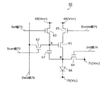
- FIG. 2 is a circuit diagram illustrating a configuration example of the pixel circuit in the embodiment.
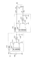
- FIG. 3 is a circuit diagram illustrating a configuration example of a part of the power supply unit according to the embodiment.
- FIG. 4A is an explanatory diagram showing the relationship between the chopping duty ratio of the VTFT power supply and the output voltage.
- FIG. 4B is a time chart showing an operation example of the VTFT power source and the VEL power source.
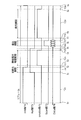
- FIG. 5 is a time chart showing a detailed timing example of the display operation.
- FIG. 6 is a circuit diagram showing a modification of the pixel circuit.
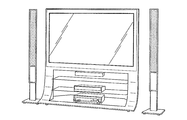
- FIG. 7 is a diagram illustrating an appearance example of the display device.
- a low voltage side power source (VEL in FIG. 2) supplied to the pixel circuit is neither 0 V nor a negative voltage but a positive voltage (for example, about 2 or 3 V). ) And should be found.
- FIG. 2 is a circuit diagram showing a configuration example of a pixel circuit used in the organic EL display device.
- the pixel circuit 60 in FIG. 2 includes a light emitting element 66, a driving transistor 61, a capacitor element 67, and a switch transistor 62 as basic components.
- the light emitting element 66 is, for example, an organic EL light emitting element and emits light with brightness according to the amount of current supplied.
- the drive transistor 61 is supplied with the voltage VTFT of the first power supply line 69 via the switch transistor 65, and supplies a current corresponding to the voltage between the gate and the source to the light emitting element 66.
- the storage capacitor element applies a voltage representing brightness (that is, a luminance voltage) between the gate and source of the driving transistor 61.
- the switch transistor 62 is a switch for writing a luminance voltage from the Data line 76 to the capacitive element 67.
- the pixel circuit 60 includes switch transistors 63, 64, and 65 as additional components.
- the additional component is to enable the operation of compensating for the variation in the threshold voltage of the drive transistor 61 between the pixel circuits by including the switch transistors 63, 64, and 65.
- the drive transistor 61 is generally a TFT (Thin Film Transistor). It has been found that the threshold voltage Vt shifts with time depending on individual usage rates.
- the switch transistors 63, 64, 65 are provided as components that enable threshold compensation operation.
- the threshold compensation operation is an operation in which the holding capacitor element 67 holds a voltage substantially equal to the actual threshold value of the driving transistor 61 immediately before the luminance voltage is written to the holding capacitor element 67 by the switch transistor 62. .
- the holding capacitor element 67 is substantially equal to (actual threshold voltage of the driving transistor 61) + (luminance voltage). Will hold the same voltage.
- the luminance voltage is 0 V
- the pixel circuit 60 becomes a black pixel (that is, the light emitting element 66 does not emit light), and thus the influence of variations in threshold voltage can be suppressed.
- the power supply VEL in the pixel circuit 60 is 0V
- the following problems may occur. That is, when the driving transistor 61 is an n-channel type and the variation in the threshold voltage Vt between the pixel circuits is large (for example, when the threshold voltage Vt varies from about 1.5 V to 5 V), 1) The above threshold compensation operation may be incomplete. As a result, (2) 0 V representing non-light-emitting black is written in the capacitor element 67 as the luminance voltage, but a little light is emitted. (3) The effective range of the voltage held in the capacitive element 67 becomes narrow. These problems can occur.
- the inventor has found that these problems can be solved by setting the power supply voltage VEL of the pixel circuit 60 to a positive voltage (eg, 2 or 3 V) instead of 0 V or a negative voltage.
- a positive voltage eg, 2 or 3 V
- a power supply device that supplies power to the pixel circuit 60 needs to generate two types of power supply voltages, ie, a power supply VTFT (for example, 20 and several V) and a power supply VEL (for example, 2, 3V).
- a power supply VTFT for example, 20 and several V
- a power supply VEL for example, 2, 3V
- two power supply circuits connected in parallel to the input voltage have an ultrashort pulse operation when the output voltage is one tenth of the input voltage in one power supply circuit. Switching loss occurs, which makes it difficult to improve power supply efficiency.
- the power supply circuit includes a transformer, the weight increases and the size increases, which makes it difficult to reduce the thickness and weight of the display device.
- This disclosure aims to provide a display device having a power supply device that improves power supply efficiency and is suitable for reduction in thickness and weight.
- FIG. 1 is a block diagram illustrating a configuration example of a display device according to an embodiment.
- FIG. 2 is a circuit diagram illustrating a configuration example of the pixel circuit in the embodiment.
- 1 is an example of an organic EL display device, and includes a control unit 2, a scanning line driving circuit 3, a power supply unit 4, a data line driving circuit 5, and a display panel 6.
- the display panel 6 is an organic EL display panel, for example, and has a plurality of pixel circuits arranged in a matrix. Each of the plurality of pixel circuits is driven by a first voltage VTFT and a positive second voltage VEL lower than the first voltage VTFT, and emits light with a light emission amount corresponding to a luminance voltage supplied from the data line driving circuit 5. It has the function to do.
- the pixel circuit 60 of FIG. 2 includes a drive transistor 61, switch transistors 62 to 65, a light emitting element 66, and a capacitive element 67.
- the Data line 76 is a data line for supplying a luminance voltage from the data line driving circuit 5.
- the reference voltage power supply line 68 is a power supply line for supplying the reference voltage VREF from the power supply unit 4.
- the reference voltage VREF is set as the potential of the first electrode of the capacitor 67 during the initialization period. The initialization period will be described later.
- the first power supply line 69 is a power supply line for supplying the first voltage VTFT from the power supply unit 4.
- the second power supply line 70 is a power supply line for supplying the second voltage VEL from the power supply unit 4.
- the initialization power supply line 71 is a power supply line for supplying the initialization voltage VINI.
- the initialization voltage VINI is set to the second electrode of the capacitor 67 during the initialization period.
- the light emitting element 66 is an organic EL element, for example, and emits light with a light emission amount corresponding to the amount of current supplied from the driving transistor 61.
- the light emitting element 66 has a cathode connected to the second power supply line 70 and an anode connected to the source of the driving transistor 61.
- the voltage supplied to the second power supply line 70 is VEL, for example, 2 to 3V.
- the driving transistor 61 is a voltage-driven driving element that controls the amount of current supplied to the light emitting element 66, and causes the light emitting element 66 to emit light by driving the current to the light emitting element 66.
- the drive transistor 61 has a gate connected to the first electrode of the capacitor 67 and a source connected to the second electrode of the capacitor 67 and the anode of the light emitting element 66.
- the switch transistor 63 is turned off, the reference voltage power supply line 68 and the first electrode of the capacitor 67 are non-conductive, and the switch transistor 65 is turned on to turn on the first power supply line 69.
- the light emitting element 66 is caused to emit light by causing a driving current, which is a current corresponding to the luminance voltage, to flow through the light emitting element 66.
- the voltage supplied to the first power supply line 69 is a VTFT, for example, 20V. Accordingly, the drive transistor 61 converts the current into a current corresponding to the luminance voltage applied between the gate and the source, and supplies the converted current to the light emitting element 66.
- the threshold voltage of the drive transistor 61 may vary from pixel circuit to pixel circuit due to a threshold voltage shift over time. The influence of this variation can be suppressed by the threshold voltage compensation operation.
- the threshold compensation operation and the threshold setting operation are simply described. This is an operation for setting a voltage corresponding to the threshold voltage of the corresponding drive transistor 61 to the capacitor 67 in each pixel circuit. Details of this operation will be described later.
- the capacitive element 67 holds a luminance voltage that determines the amount of current that the driving transistor 61 flows.
- the second electrode (electrode on the node B side) of the capacitive element 67 is connected to the source of the driving transistor 61 and the anode of the light emitting element 66.
- the second electrode of the capacitive element 67 is connected to the initialization power supply line 71 via the switch transistor 64.
- a first electrode (electrode on the node A side) of the capacitive element 67 is connected to the gate of the driving transistor 61.
- the first electrode of the capacitive element 67 is connected to the reference voltage power line 68 (VREF) via the switch transistor 63.
- the switch transistor 62 switches between conduction and non-conduction between the Data line 76 for supplying the luminance voltage and the first electrode of the capacitor 67.
- the switch transistor 62 has one of drain and source terminals connected to the Data line 76, the other drain and source terminal connected to the first electrode of the capacitor 67, and a gate connected to the Scan line 72. It is a connected switching transistor.
- the switch transistor 62 has a function for writing a luminance voltage corresponding to the video signal voltage (video signal) supplied via the Data line 76 to the capacitor 67.
- the switch transistor 63 switches between conduction and non-conduction between the reference voltage power supply line 68 that supplies the reference voltage VREF and the first electrode of the capacitive element 67.
- the switch transistor 63 one terminal of the drain and the source is connected to the reference voltage power supply line 68, the other terminal of the drain and the source is connected to the first electrode of the capacitor 67, and the gate is the Ref line.
- 73 is a switching transistor connected to 73.
- the switch transistor 63 has a function of applying the reference voltage VREF to the first electrode of the capacitor 67.
- the switch transistor 64 switches between conduction and non-conduction between the second electrode of the capacitive element 67 and the initialization power supply line 71. Specifically, in the switch transistor 64, one terminal of the drain and the source is connected to the initialization power supply line 71, the other terminal of the drain and the source is connected to the second electrode of the capacitor 67, and the gate is the Init line. 74 is a switching transistor connected to 74. In other words, the switch transistor 64 has a function of applying the initialization voltage VINI to the second electrode of the capacitor 67.
- the switch transistor 65 switches between conduction and non-conduction between the first power supply line 69 and the drain electrode of the drive transistor 61.
- the switch transistor 65 has one terminal of the drain and the source connected to the first power supply line 69, the other terminal of the drain and the source is connected to the drain electrode of the driving transistor 61, and the gate is the enable line 75. Is a switching transistor connected to.
- the pixel circuit 60 is configured as described above.
- the switch transistors 62 to 65 constituting the pixel circuit 60 will be described below as n-type TFTs, but are not limited thereto.
- the switch transistors 62 to 65 may be p-type TFTs.
- an n-type TFT and a p-type TFT may be used in a mixed manner. Note that the voltage level described below may be reversed for the signal line connected to the gate of the p-type TFT.
- the potential difference between the reference voltage VREF of the reference voltage power supply line 68 and the initialization voltage VINI of the initialization power supply line 71 is set to a voltage larger than the maximum threshold voltage of the drive transistor 61.
- the reference voltage VREF of the reference voltage power supply line 68 and the initialization voltage VINI of the initialization power supply line 71 are set as follows so that no current flows through the light emitting element 66.
- Initialization voltage VINI ⁇ reference voltage VEL + (forward current threshold voltage of light emitting element 66), (reference voltage VREF of reference voltage power line 68) ⁇ second voltage VEL + (forward current threshold voltage of light emitting element 66) ) + (Threshold voltage of drive transistor 61)
- the second voltage VEL is the voltage of the second power supply line 70 as described above. In order to satisfy these conditions, it is desirable that the second voltage VEL is about positive 2 or 3V.
- the pixel circuit 60 is configured as described above. Next, the configuration of FIG. 1 will be described.
- the control unit 2 in FIG. 1 controls the entire display device 1. Specifically, the control unit 2 controls the display operation for each frame based on the video signal to be displayed.
- the scanning line driving circuit 3 drives and scans the gate signals for the plurality of pixel circuits of the display panel 6 based on the control of the control unit 2.
- a Scan signal a Ref signal
- an Enable signal an Enable signal
- an Init signal More specifically, the scanning line driving circuit 3 outputs a Scan signal, a REF signal, an Enable signal, and an init signal based on a vertical synchronization signal and a horizontal synchronization signal included in a video signal to be displayed, in a row unit of the pixel circuit. Scan with.
- FIG. 1 In the pixel circuit example shown in FIG.
- these Scan signal, Ref signal, Enable signal, and Init signal are output to the Scan line 72, the Ref line 73, the Enable line 75, and the Init line 74, and the connection destination switch is turned on and off. Used to control off.
- the power supply unit 4 supplies power to each unit of the control unit 2, the scanning line driving circuit 3, and the display panel 6, and supplies various voltages to the display panel 6.
- the various voltages referred to here are the first voltage VTFT, the second voltage VEL, the initialization voltage VINI, and the reference voltage VREF, and the initialization power line 71, the reference voltage power line 68,
- the pixel circuit 60 is supplied via the first power line 69 and the second power line 70.
- the second voltage is 2 to 3 V instead of 0 V, and is generated by the power supply unit 4.
- the data line drive circuit 5 outputs a luminance voltage using the data line 76 of the display panel 6 as a source signal based on the control of the control unit 2. More specifically, the data line driving circuit 5 outputs a source signal to each pixel circuit based on the video signal and the horizontal synchronization signal.
- the display device 1 is configured.
- FIG. 3 is a circuit diagram illustrating a circuit example of the power supply unit and the pixel circuit 60 in the embodiment.
- generates the 1st voltage VTFT and the 2nd voltage VEL among the circuit structures of the power supply part 4 is shown.
- only one of the plurality of pixel circuits 60 is simplified and shown as a representative.
- the power supply unit 4 includes an input capacitor 409, a VTFT power supply 410, and a VEL power supply 420.
- the VTFT power supply 410 is also called a first power supply circuit
- the VEL power supply 420 is also called a second power supply circuit.
- the input voltage Vin is a direct current voltage of 30 or more volts supplied from the input power line 401.
- the input capacitor 409 is connected between the input power supply line 401 near the input end of the VTFT power supply 410 and the ground line, and is a capacitance element for stabilizing the input voltage Vin and cutting noise.
- the VTFT power supply 410 (that is, the first power supply circuit) is a synchronous rectification type power supply circuit that outputs the first voltage VTFT to the first power supply line 69 by chopping the input voltage Vin.
- the VTFT power supply 410 includes a first high-side switch 411, a first low-side switch 412, a first inductor 413, a first control circuit 414, and a first output capacitor 419.
- the first high-side switch 411 and the first low-side switch 412 are connected in series between the input power supply line 401 to which the input voltage Vin is applied and the ground line, and each is, for example, a power MOSFET.
- the first high-side switch 411 and the first low-side switch 412 are controlled so as to be exclusively turned on by the first control circuit 414.
- the first inductor 413 is an induction element, that is, a coil, one end of which is connected to a connection point between the first high side switch 411 and the first low side switch 412 and the other end is connected to the first power line 69.
- the electric energy by the input voltage Vin applied from one end is accumulated, and the electric energy is supplied from the other end to the first power supply line 69. introduce.
- the first inductor 413 discharges the stored electrical energy from the other end to the first power line 69 when the first high-side switch 411 is off and the first low-side switch 412 is on.
- the first control circuit 414 controls on and off of the first high-side switch 411 and the first low-side switch 412, and the first high-side switch so that the first voltage VTFT of the first power supply line 69 becomes a desired voltage.
- the duty ratio which is the ratio of the ON period 411, is controlled.
- the desired voltage as the first voltage VTFT is, for example, 20 V in the display device of FIG.
- control is performed so that the first high-side switch 411 and the first low-side switch 412 are not turned on at the same time.
- the first output capacitor 419 is connected between the first power supply line 69 and the ground line, and smoothes the voltage generated by the electric energy emitted from the other end of the first inductor 413, stabilizes the voltage, and reduces noise. It is a capacitive element for cutting.
- the first output capacitor 419 also functions as an input capacitance element for the VEL power supply 420. Therefore, it is not necessary to provide the VEL power supply 420 with a separate input capacitance element, and the first output capacitor 419 can suppress a ripple current by a regenerative operation in the VEL power supply 420 described later, and can use a smaller capacitor capacity. Cost can be reduced.
- the VEL power supply 420 receives not the input voltage Vin but the first voltage VTFT having a voltage lower than the input voltage Vin.
- the VEL power supply 420 (that is, the second power supply circuit) is a synchronous rectification type power supply circuit that outputs the second voltage VEL to the second power supply line 70 by chopping the first voltage VTFT. As shown in FIG. 3, the VEL power supply 420 includes a second high side switch 421, a second low side switch 422, a second inductor 423, a second control circuit 424, and a second output capacitor 429.
- the second high-side switch 421 and the second low-side switch 422 are connected in series between the input power line 401 to which the first voltage VTFT is applied and the ground line, and each is, for example, a power MOSFET.
- the second high side switch 421 and the second low side switch 422 are controlled to be exclusively turned on by the second control circuit 424.
- the second inductor 423 is an induction element, that is, a coil, one end of which is connected to a connection point between the second high-side switch 421 and the second low-side switch 422 and the other end is connected to the second power supply line 70.
- the second high-side switch 421 is on and the second low-side switch 422 is off, electric energy is accumulated by the first voltage VTFT applied from one end, and electric energy is applied from the other end to the second power supply line 70.
- the second inductor 423 releases the stored electrical energy from the other end to the second power supply line 70 when the second high-side switch 421 is off and the second low-side switch 422 is on.
- the second control circuit 424 controls on and off of the second high-side switch 421 and the second low-side switch 422 so that the second voltage VEL of the second power supply line 70 becomes a desired voltage.
- the duty ratio which is a ratio of the ON period 421 is controlled.
- the desired voltage as the second voltage VEL is, for example, 2 V or 3 V in the display device of FIG.
- the second control circuit 424 controls the second high side switch 421 and the second low side switch 422 so that they are not turned on at the same time.
- the second output capacitor 429 is connected between the second power supply line 70 and the ground line, and smoothes the voltage generated by the electric energy emitted from the other end of the second inductor 423, stabilizes the voltage, and reduces noise. It is a capacitive element for cutting.
- the VEL power supply 420 has the same configuration as the VTFT power supply 410, but circuit constants differ depending on the output voltage.
- the current flowing through the pixel circuit 60 is sucked into the second power supply line instead of the ground line.
- the current flowing through the light emitting element 66 in the plurality of pixel circuits 60 of the display panel 6 is sucked into the second power supply line 70.
- a part of this current is stored and reused as electric energy in the second high-side switch 421 and the second output capacitor 429, and the other part is passed through the second inductor 423 and the second high-side switch 421. It flows as a regenerative current in one power line 69. This reuse and regenerative current improves power supply efficiency.
- the power supply unit 4 is configured as described above.
- the specific values of the input voltage, the first voltage, and the second voltage are the characteristics of the TFT that is the drive transistor 61 (for example, the threshold voltage of the drive transistor 61, the magnitude of the threshold shift, etc.) It should be determined according to 66 characteristics (for example, forward current threshold voltage).
- the input voltage, the first voltage, and the second voltage may be 30V, 20V, and 2V, respectively.
- the input voltage may be 30 several volts
- the first voltage may be in the range of 15V to 25V
- the second voltage may be a positive voltage of 5V or less.
- FIG. 4A is an explanatory diagram showing the relationship between the switching duty ratio of the VTFT power supply 410 and the output voltage.
- the horizontal axis is the time axis
- the vertical axis is the voltage.
- the chopped input voltage that is, the pulsed input voltage input to one end of the first inductor 413
- the first voltage VTFT as the output voltage Is schematically illustrated.
- the duty of the ON time of the first high-side switch 411 is controlled according to the output voltage and the output current, so that it is stable even when the load fluctuates. Output can be obtained.
- the input voltage Vin, the first voltage VTFT as the output voltage, and the duty ⁇ have the following relationship.
- the duty ⁇ is the ON time in the first high-side switch 411 / (ON time + OFF time).
- PWM Pulse Width Modulation
- the duty ⁇ is the ON time / (ON time + OFF time) in the second high-side switch 421.
- the second control circuit 424 switches the second high-side switch 421 at a frequency of, for example, one hundred and several tens kHz with this duty.
- FIG. 4B is a time chart showing an operation example of the VTFT power source and the VEL power source.
- the vertical and horizontal axes in FIG. 4B are the same as those in FIG. 4A.
- the left side of the figure shows a pulsed input voltage input to one end of the first inductor 413 in the VTFT power supply 410 and a first voltage VTFT which is an output voltage.
- the right side of the figure shows a pulsed input voltage input to one end of the second inductor 423 in the VEL power supply 420 and a second voltage VEL that is an output voltage.
- the VTFT power supply 410 and the VEL power supply 420 in the power supply unit 4 are not connected in parallel to the input voltage Vin, but the VEL power supply 420 has a first voltage VTFT having a voltage lower than the input voltage Vin. Is entered. As a result, the duty ratio is prevented from becoming extremely small, and the output voltage is easily stabilized.
- the first low-side switch 412 in the VTFT power supply 410 can also use a diode with its anode grounded instead of the power MOSFET. However, since a loss occurs due to a forward voltage drop in the diode, the power MOSFET is superior to the diode from the viewpoint of improving the power supply efficiency.
- the second low-side switch 422 in the VEL power supply 420 cannot be replaced in principle because of the regenerative (boost) operation described above.
- the second high-side switch 421 can be regenerated by diode replacement, but the second voltage VEL cannot be maintained if there is a period during which no current flows through the light emitting element 66 (T26, T28, T30 in FIG. 5). The operation of the VEL power supply 420 is insufficient. As a result, the second high-side switch 421 and the second low-side switch 421 cannot be diodeized.
- FIG. 5 is a time chart showing a detailed timing example of the display operation.
- the horizontal axis represents the time axis
- the vertical axis represents the control signals of the Init line 74, the Ref line 73, the Enable line 75, the Scan line 72, and the Data line 76 in the pixel circuit of FIG.
- the figure shows a display operation in one frame period.
- the voltage corresponding to the threshold voltage of the drive transistor 61 is held in the capacitor element 67 in each pixel circuit 60 at the end of the period T25 by the threshold voltage guarantee operation. . This compensates for variations in threshold voltage. This will be specifically described below.
- Period T21 A period T21 from time t0 to time t1 shown in FIG. 5 is a period for setting only the switch transistor 64 in the conductive state and setting the potential of the node B in FIG. 2 to the initialization voltage VINI of the initialization power supply line 71. .
- the capacity of the light emitting element 66 is increased, and the wiring time constant of the initialization power supply line 71 is increased. It takes time to set the voltage to the initialization voltage VINI of the initialization power supply line 71. Therefore, by providing the period T21 in which the switch transistor 64 is first turned on, the potential of the node B can be reliably set by the initialization voltage VINI of the initialization power supply line 71.
- the target for charging / discharging the reference voltage VREF is the wiring time constant of the capacitive element 67 and the reference voltage power supply line 68. That is, the wiring time constants of the reference voltage power supply line 68 and the initialization power supply line 71 are substantially equal, but (capacity of the light emitting element 66)> (capacitance of the capacitive element 67), and the capacitance ratio (light emitting element 66). Capacity) / (capacitance element 67 capacity) is 1.3 to 9 times.
- charging the light emitting element 66 (writing the initialization voltage VINI of the initialization power supply line 71 to the potential of the node B) charges the capacitor element 67 (charging the reference voltage VREF of the reference voltage power supply line 68 to the potential of the node A). It takes longer than writing).
- the load for writing the initialization voltage VINI of the reference voltage power supply line 68 to the node A can be reduced.
- the voltage of the node A can be set to a low voltage, and the reference voltage power line 68 only needs to supply a current (voltage) for charging the pixel circuit 60.
- the reference voltage VREF of the reference voltage power supply line 68 is not used as a voltage for charging the light emitting element 66, there is an advantage that the load on the reference voltage power supply line 68 is reduced.
- the period T21 for determining the potential of the node B is provided first. Thereby, the total time of the period T22 after the period T21 can be shortened while reducing the power consumption of the display panel 6 and the influence of the luminance fluctuation of the display panel 6.
- Period T22 Initialization period
- the capacitor 67 holds the initial voltage necessary for flowing the drain current for compensating the threshold voltage of the drive transistor 61, and the source of the drive transistor 61 This is an initialization period for applying between the gates.
- the potential of the node A is set to the reference voltage VREF of the reference voltage power line 68.
- the potential of the node B is already set to the initialization voltage VINI of the initialization power supply line 71. That is, the reference voltage VREF of the reference voltage power supply line 68 and the initialization voltage VINI of the initialization power supply line 71 are applied to the gate and source of the drive transistor 61, respectively.
- period T22 is set to a length (time) until the potentials of the nodes A and B are stabilized.
- the gate-source voltage of the driving transistor 61 needs to be set to an initial voltage that can secure an initial drain current necessary for performing the threshold compensation operation. That is, the initial voltage needs to be higher than the threshold voltage of the driving transistor 61 in each of the capacitor elements 67 of the plurality of pixel circuits 60 and not to cause the light emitting element 66 to emit light. Therefore, the potential difference between the reference voltage VREF of the reference voltage power supply line 68 and the initialization voltage VINI of the initialization power supply line 71 is set to a voltage larger than the maximum threshold voltage of the drive transistor 61.
- the reference voltage VREF and the initialization voltage VINI are set such that the initialization voltage VINI ⁇ (the second voltage VEL + the forward current threshold voltage of the light emitting element 66) and VREF ⁇ so that no current flows through the light emitting element 66. (The second voltage VEL + the forward current threshold voltage of the light emitting element 66 + the threshold voltage of the driving transistor 61).
- the second voltage VEL In order to satisfy these conditions, it is easy for the second voltage VEL to be 2V or 3V instead of 0V to satisfy these conditions. Further, the influence of the threshold shift of the drive transistor 61 can be suppressed by the threshold voltage compensation operation.
- Period T23 A period T23 from time t2 to time t3 shown in FIG. 5 is a period for preventing the switch transistor 64 and the switch transistor 65 from being in a conductive state at the same time.
- the switch transistor 64 and the switch transistor 65 are turned on at the same time without the period T23. It is possible to prevent a through current from flowing between the first power supply line 69 and the initialization power supply line 71 via 61 and the switch transistor 64.
- a period T24 from time t3 to time t4 in FIG. 5 is a threshold setting period for compensating for variation in threshold voltage of the drive transistor 61 in the plurality of pixel circuits 60. That is, it is a period in which a voltage corresponding to the threshold voltage of each driving transistor 61 is set in the corresponding capacitor element 67 even if the threshold voltages of the driving transistors 61 in the plurality of pixel circuits 60 vary.
- the switch transistor 62 and the switch transistor 64 are in a non-conductive state (off state), and the switch transistor 63 is maintained in a conductive state (on state), while the switch transistor 65 is in a conductive state (on state).
- the drive transistor 61 is supplied with a drain current by the first voltage VTFT of the first power supply line 69, and the source potential of the drive transistor 61 changes with it.
- the source potential of the drive transistor 61 changes until the drain current supplied by the first voltage VTFT of the first power supply line 69 becomes zero.
- the voltage at the node A and the node B (that is, the gate-source voltage of the driving transistor 61) is a voltage corresponding to the actual threshold value of the driving transistor 61. This voltage is held in the capacitive element 67.
- a voltage corresponding to the actual threshold value of the driving transistor 61 is held in the capacitor element 67. Accordingly, a voltage representing luminance written to the capacitor 67 after the period T25 is prevented from being shifted from a correct value by a threshold voltage shift due to variation in threshold voltage.
- Period T25 A period T25 from time t4 to time t5 shown in FIG. 5 is a period for ending the threshold compensation operation.
- each capacitor element 67 in the plurality of pixel circuits 60 holds a voltage corresponding to the actual threshold voltage of the corresponding drive transistor 61. .
- Period T26 During a period T26 from time t5 to time t6, the data transistor voltage supplied via the data line 76 and the reference voltage VREF of the reference voltage power supply line 68 are changed by turning off the switch transistor 63. At the same time, it is a period for preventing application to the node A.
- Period T27 Write period
- a period T27 from time t6 to time t7 is a writing period in which the luminance voltage corresponding to the display gradation is taken from the data line 76 into the pixel circuit 60 via the switch transistor 62 and written into the capacitor 67.
- the switch transistor 63, the switch transistor 64, and the switch transistor 65 are maintained in a non-conductive state (off state), while the switch transistor 62 is set in a conductive state (on state).
- the voltage difference between the luminance voltage and the reference voltage VREF of the reference voltage power supply line 68 is (capacitance of the light emitting element 66). ) / (Capacitance of the light emitting element 66 + capacitance of the capacitive element 67) and is held in the capacitive element 67. Since the switch transistor 65 is in a non-conductive state, the drive transistor 61 does not pass a drain current.
- the voltage corresponding to the luminance voltage from the Data line 76 and the actual threshold voltage of the driving transistor 61 is held in the capacitor element 67.
- Period T28 A period T28 from time t7 to time t8 is a period for surely turning off the switch transistor 62.
- Period T29 Light emission period
- the switch transistor 62, the switch transistor 63, and the switch transistor 64 are maintained in the off state, and the switch transistor 65 is in the on state.
- the switch transistor 65 By turning on the switch transistor 65, current is supplied to the light emitting element 66 to the driving transistor 61 in accordance with the voltage stored in the capacitor 67 to cause the light emitting element 66 to emit light.
- Period T30 A period T30 from time t9 to time t0 is a period for setting all the switches in a non-conductive state and changing the potentials of the nodes A and B to a voltage close to the voltage required in the period T21.
- the display panel 6 performs display according to the sequence as described above. Further, as already described, the threshold voltage compensation operation in the period T24 is performed when the driving transistor 61 is an n-channel type and the threshold voltage Vt varies greatly between pixel circuits (for example, the threshold voltage). When the voltage Vt varies from about 1.5V to 5V), it may not function effectively. That is, (1) the threshold compensation operation may be incomplete. As a result, (2) 0 V representing non-light-emitting black is written in the capacitor element 67 as the luminance voltage, but a little light is emitted. (3) The effective range of the voltage held in the capacitive element 67 becomes narrow. These problems can occur.
- the power supply unit 4 that supplies power to the pixel circuit 60 generates two types of power supply voltages: a first voltage VTFT (for example, 20 several V) and a positive second voltage VEL (for example, 2, 3V) that is not 0V. And supplied to a plurality of pixel circuits 60. As a result, the function of suppressing the influence of the threshold shift of the drive transistor 61 by the threshold voltage compensation operation can be used effectively.
- a first voltage VTFT for example, 20 several V
- a positive second voltage VEL for example, 2, 3V
- the VEL power supply 420 which is the second power supply circuit that generates the second voltage, chops the first power supply VTFT having a voltage lower than the input voltage Vin, so the input voltage Vin is chopped.
- the transition loss of the switching element instability of the switching operation due to the extremely small duty ratio can be avoided, and the second voltage can be stabilized.
- the VTFT power supply 410 that is the first power supply circuit and the VEL power supply 420 that is the second power supply circuit do not include a transformer, it is easy to reduce the thickness and weight.
- the output voltage is determined according to the chopping duty ratio, it is easy to change the output voltage and fine-tune the output voltage.
- the transformer winding that is, change the number of windings and the winding ratio
- the output voltage can be easily changed and finely adjusted.
- the threshold compensation operation can be made to function more completely.
- the display device includes the first power supply line maintained at the first voltage and the second power supply line maintained at the positive second voltage lower than the first voltage.
- a plurality of pixel circuits arranged in a matrix to receive power supply from the first, a synchronous rectification type first power supply circuit that outputs the first voltage to the first power supply line by chopping an input voltage, and the first A synchronous rectification type second power supply circuit that outputs the second voltage to the second power supply line by chopping one voltage.
- the first power supply circuit includes a first high side switch and a first low side switch connected in series between an input power supply line to which the input voltage is applied and a ground line, and one end of the first power supply circuit and the first high side switch A first inductor connected to a connection point with the first low-side switch and having the other end connected to the first power supply line, and a first for controlling on and off of the first high-side switch and the first low-side switch And a controller.
- the second power supply circuit includes a second high-side switch and a second low-side switch connected in series between the first power supply line and the ground line, and one end of the second high-side switch and the second low-side switch. And a second controller having the other end connected to the second power supply line, and a second controller for controlling on and off of the second high-side switch and the second low-side switch. .
- the power supply efficiency can be improved compared to chopping the input voltage.
- the power supply efficiency can be further improved.
- the duty ratio can be prevented from becoming extremely small, and the second voltage can be stabilized.
- the first power supply circuit and the second power supply circuit do not include a transformer, it is easy to reduce the thickness and weight.
- the output voltage is determined according to the chopping duty ratio, it is easy to change the output voltage and fine-tune the output voltage.
- the transformer winding that is, change the number of windings and the winding ratio
- the output voltage can be easily changed and finely adjusted.
- each of the plurality of pixel circuits includes a light emitting element that emits light with brightness according to a supplied current amount, and a driving transistor that supplies current to the light emitting element, and the driving transistor and the light emitting element May be connected in series between the first power line and the second power line.
- the display device further includes an input capacitor connected between the input power line and the ground line, a first output capacitor connected between the first power line and the ground line, A second output capacitor connected between the second power supply line and the ground line may be provided.
- the second power supply circuit since the first output capacitor also functions as an input capacitance element of the second power supply circuit, the second power supply circuit does not need to include a separate input capacitance element, and the first output capacitor is The regenerative operation suppresses the ripple current, allows the use of a smaller capacitor capacity, and reduces the cost.
- each of the plurality of pixel circuits includes a capacitive element connected to a gate of the driving transistor
- the display device includes a control unit that controls display of the plurality of pixel circuits
- the control unit includes: The threshold value compensation operation is performed to hold the voltage corresponding to the actual threshold voltage of the drive transistor to which the capacitor element is connected, and the voltage corresponding to the actual threshold voltage is held.
- a writing operation in which a voltage representing luminance is added to the capacitor may be performed.
- the function of suppressing the influence of the threshold shift of the drive transistor due to the threshold voltage compensation operation can be used more effectively.
- FIG. 6 is a diagram illustrating a configuration example of the pixel circuit 60 in the modification.
- the display device 1 may include a pixel circuit 60 illustrated in FIG. 6 instead of the pixel circuit 60 illustrated in FIG.
- the pixel circuit 60 of FIG. 6 differs from that of FIG. 1 in that the switch transistor 63, the switch transistor 64, and the switch transistor 65 are deleted. In this way, the configuration of the pixel circuit 60 may be simplified.
- the display device has been described based on the embodiment, but the present disclosure is not limited to this embodiment.
- the technology in the present disclosure is not limited to these, and can also be applied to embodiments in which changes, replacements, additions, omissions, and the like have been made as appropriate.
- various modifications conceived by those skilled in the art have been made in this embodiment, and forms constructed by combining components in different embodiments are also within the scope of one or more aspects. Contained within.
- the display device described above can be used as a flat panel display as shown in FIG. 7, for example.
- the present invention can be applied to all electronic devices having a display device such as a television receiver, a personal computer, and a mobile phone.
- the present disclosure can be used for a display device such as a television receiver or a display of an information device.
Landscapes
- Engineering & Computer Science (AREA)
- Physics & Mathematics (AREA)
- Computer Hardware Design (AREA)
- General Physics & Mathematics (AREA)
- Theoretical Computer Science (AREA)
- Control Of Indicators Other Than Cathode Ray Tubes (AREA)
- Control Of El Displays (AREA)
- Dc-Dc Converters (AREA)
- Electroluminescent Light Sources (AREA)
Abstract
Description
本発明者は、例えば図2に示すような画素回路において、画素回路に供給される低電圧側の電源(図2のVEL)が0Vでも負の電圧でもなく正の電圧(例えば2、3V程度)とすべきであることを見出した。
以下、適宜図面を参照しながら、実施の形態を詳細に説明する。但し、必要以上に詳細な説明は省略する場合がある。例えば、既によく知られた事項の詳細説明や実質的に同一の構成に対する重複説明を省略する場合がある。これは、以下の説明が不必要に冗長になるのを避け、当業者の理解を容易にするためである。
図1は、実施の形態における表示装置の構成例を示すブロック図である。図2は、実施の形態における画素回路の構成例を示す回路図である。
図2の画素回路60は、駆動トランジスタ61と、スイッチトランジスタ62~65と、発光素子66と、容量素子67とを備えている。また、Data線76は、データ線駆動回路5から輝度電圧を供給するためのデータ線である。基準電圧電源線68は、電源部4から基準電圧VREFを供給するための電源線である。基準電圧VREFは、初期化期間に容量素子67の第1電極の電位として設定される。初期化期間については後述する。第1電源線69は、電源部4から第1電圧VTFTを供給するための電源線である。第2電源線70は、電源部4から第2電圧VELを供給するための電源線である。初期化電源線71は初期化電圧VINIを供給するための電源線である。初期化電圧VINIは、初期化期間に容量素子67の第2電極に設定される。
次に電源部4の構成について説明する。図3は、実施の形態における電源部の回路例と、画素回路60をと示す回路図である。同図では、電源部4の回路構成のうち、主として第1電圧VTFTおよび第2電圧VELを生成する回路部分を示している。同図では、複数の画素回路60のうちの1つのみ代表として簡略化し図示している。
VTFT電源410(つまり第1電源回路)は、入力電圧Vinをチョッピングすることにより第1電源線69に第1電圧VTFTを出力する同期整流型の電源回路である。このVTFT電源410は、第1ハイサイドスイッチ411、第1ローサイドスイッチ412、第1インダクタ413、第1制御回路414、第1出力キャパシタ419を備える。
VEL電源420には、上記の入力電圧Vinではなく、入力電圧Vinよりも低い電圧の第1電圧VTFTが入力される。
次に、図3に示した電源装置の動作および図1に示した表示装置の動作について説明する。
図4Aは、VTFT電源410のスイッチングのデューティ比と出力電圧の関係を示す説明図である。図4Aにおいて横軸は時間軸、縦軸は電圧であり、チョッピングされた入力電圧(つまり第1インダクタ413の一端に入力されるパルス状の入力電圧)と、出力電圧である第1電圧VTFTとを模式的に図示してある。
VEL電源420の動作については、基本的にVTFT電源410と同様であるので、異なる点を中心に説明する。VEL電源420では、入力電圧である第1電圧VTFT、出力電圧である第2電圧、デューティβには次の関係がある。
次に、表示パネルにおける、既に触れたしきい値電圧補償動作を含む表示動作について説明する。
図5に示す時刻t0~時刻t1の期間T21は、スイッチトランジスタ64のみを導通状態であり、図2の節点Bの電位を初期化電源線71の初期化電圧VINIに設定するための期間である。
図5に示す時刻t1~時刻t2の期間T22は、駆動トランジスタ61のしきい値電圧補償を行うためのドレイン電流を流すのに必要な初期電圧を容量素子67に保持させ、駆動トランジスタ61のソースゲート間に印加するための初期化期間である。
図5に示す時刻t2~時刻t3の期間T23は、スイッチトランジスタ64とスイッチトランジスタ65とが同時に導通状態とならないようにするための期間である。
次に、図5の時刻t3~時刻t4の期間T24は、複数の画素回路60における駆動トランジスタ61のしきい値電圧のばらつきを補償するしきい値設定期間である。つまり、複数の画素回路60における駆動トランジスタ61のしきい値電圧にばらつきがあっても、個々の駆動トランジスタ61のしきい値電圧に相当する電圧を対応する容量素子67に設定する期間である。
図5に示す時刻t4~時刻t5の期間T25は、しきい値補償動作を終了させるための期間である。
時刻t5~時刻t6の期間T26は、スイッチトランジスタ63を非導通状態(オフ状態)にすることで、Data線76を介して供給されたデータ信号電圧と基準電圧電源線68の基準電圧VREFとが同時に節点Aに印加されるのを防止する期間である。
時刻t6~時刻t7の期間T27は、Data線76から表示階調に応じた輝度電圧を画素回路60にスイッチトランジスタ62を介して取り込み、容量素子67に書き込む書込期間である。
時刻t7~時刻t8の期間T28は、スイッチトランジスタ62を確実に非導通にさせるための期間である。
次に、時刻t8~時刻t9の期間T29は、発光期間である。
刻t9~時刻t0の期間T30は、すべてのスイッチを非導通状態として、節点Aおよび節点Bの電位を、期間T21で必要な電圧に近い電圧まで変化させるための期間である。
本実施の形態における表示装置によれば、第2電圧を生成する第2電源回路であるVEL電源420が入力電圧Vinよりも低い電圧の第1電源VTFTをチョッピングするので、入力電圧Vinをチョッピングすることと比べて、スイッチング素子の遷移損失を軽減させることで、ディーティ比が極端に小さくなることによるスイッチング動作の不安定化を回避することができ、第2電圧を安定化することができる。
図6は、変形例における画素回路60の構成例を示す図である。表示装置1は、図2に示した画素回路60の代わりに図6に示す画素回路60を備える構成としてもよい。図6の画素回路60は、図1と比べて、スイッチトランジスタ63、スイッチトランジスタ64およびスイッチトランジスタ65が削除されている点が異なる。このように画素回路60の構成を単純化してもよい。
2 制御部
3 走査線駆動回路
4 電源部
5 データ線駆動回路
6 表示パネル
60 画素回路
61 駆動トランジスタ
62、63、64、65 スイッチトランジスタ
66 発光素子
67 容量素子
68 基準電圧電源線
69 第1電源線
70 第2電源線
71 初期化電源線
72 Scan線
73 Ref線
74 Init線
75 Enable線
76 Data線
401 入力電源線
409 入力キャパシタ
410 VTFT電源
411 第1ハイサイドスイッチ
412 第1ローサイドスイッチ
413 第1インダクタ
414 第1制御回路
419 第1出力キャパシタ
420 VEL電源
421 第2ハイサイドスイッチ
422 第2ローサイドスイッチ
423 第2インダクタ
424 第2制御回路
429 第2出力キャパシタ
Vin 入力電圧
VTFT 第1電圧
VEL 第2電圧
Claims (4)
- 第1電圧に維持される第1電源線と、前記第1電圧より低い正の第2電圧に維持される第2電源線とから電力供給を受ける行列状に配置された複数の画素回路と、
入力電圧をチョッピングすることにより前記第1電源線に前記第1電圧を出力する同期整流型の第1電源回路と、
前記第1電圧をチョッピングすることにより前記第2電源線に前記第2電圧を出力する同期整流型の第2電源回路と
を備え、
前記第1電源回路は、
前記入力電圧が印加される入力電源線と接地線の間に直列に接続された第1ハイサイドスイッチおよび第1ローサイドスイッチと、
一端が前記第1ハイサイドスイッチと前記第1ローサイドスイッチとの接続点に接続され、他端が前記第1電源線に接続された第1インダクタと、
前記第1ハイサイドスイッチおよび前記第1ローサイドスイッチのオンおよびオフを制御する第1コントローラと
を備え、
前記第2電源回路は、
前記第1電源線と前記接地線の間に直列に接続された第2ハイサイドスイッチおよび第2ローサイドスイッチと、
一端が前記第2ハイサイドスイッチと前記第2ローサイドスイッチとの接続点に接続され、他端が前記第2電源線に接続された第2インダクタと、
前記第2ハイサイドスイッチおよび前記第2ローサイドスイッチのオンおよびオフを制御する第2コントローラと
を備える表示装置。 - 前記複数の画素回路のそれぞれは、
供給される電流量に応じた明るさで発光する発光素子と、
前記発光素子に電流を供給する駆動トランジスタと
を備え、
前記駆動トランジスタおよび前記発光素子は、前記第1電源線と前記第2電源線との間に直列に接続される
請求項1に記載の表示装置。 - 前記表示装置は、さらに
前記入力電源線と前記接地線との間に接続された入力キャパシタと、
前記第1電源線と前記接地線との間に接続された第1出力キャパシタと、
前記第2電源線と前記接地線との間に接続された第2出力キャパシタと
を備える
請求項1または2に記載の表示装置。 - 前記複数の画素回路のそれぞれは、前記駆動トランジスタのゲートに接続された容量素子を備え、
前記表示装置は、前記複数の画素回路の表示を制御する制御部を備え、
前記制御部は、
前記容量素子に、当該容量素子が接続された前記駆動トランジスタの実際のしきい値電圧に相当する電圧を保持させるしきい値補償動作を行い、
実際のしきい値電圧に相当する電圧が保持された前記容量素子に、輝度を表す電圧を上乗せする書き込み動作を行う
請求項2に記載の表示装置。
Priority Applications (2)
| Application Number | Priority Date | Filing Date | Title |
|---|---|---|---|
| US15/116,316 US9953570B2 (en) | 2014-02-05 | 2014-12-24 | Display device |
| JP2015560868A JP6206512B2 (ja) | 2014-02-05 | 2014-12-24 | 表示装置 |
Applications Claiming Priority (2)
| Application Number | Priority Date | Filing Date | Title |
|---|---|---|---|
| JP2014-020645 | 2014-02-05 | ||
| JP2014020645 | 2014-02-05 |
Publications (1)
| Publication Number | Publication Date |
|---|---|
| WO2015118601A1 true WO2015118601A1 (ja) | 2015-08-13 |
Family
ID=53777442
Family Applications (1)
| Application Number | Title | Priority Date | Filing Date |
|---|---|---|---|
| PCT/JP2014/006420 Ceased WO2015118601A1 (ja) | 2014-02-05 | 2014-12-24 | 表示装置 |
Country Status (3)
| Country | Link |
|---|---|
| US (1) | US9953570B2 (ja) |
| JP (1) | JP6206512B2 (ja) |
| WO (1) | WO2015118601A1 (ja) |
Cited By (2)
| Publication number | Priority date | Publication date | Assignee | Title |
|---|---|---|---|---|
| EP3327713A1 (en) * | 2016-11-29 | 2018-05-30 | LG Display Co., Ltd. | Organic light-emitting display and driving method thereof |
| JP2024072543A (ja) * | 2022-11-16 | 2024-05-28 | JDI Design and Development 合同会社 | 表示装置 |
Families Citing this family (4)
| Publication number | Priority date | Publication date | Assignee | Title |
|---|---|---|---|---|
| WO2017012075A1 (zh) * | 2015-07-21 | 2017-01-26 | 深圳市柔宇科技有限公司 | 像素电路及其驱动方法、显示面板 |
| CN106652904B (zh) | 2017-03-17 | 2019-01-18 | 京东方科技集团股份有限公司 | 像素驱动电路及其驱动方法、显示装置 |
| KR102295068B1 (ko) * | 2017-03-31 | 2021-08-31 | 삼성디스플레이 주식회사 | 표시 장치 및 그의 구동 방법 |
| TWI726716B (zh) * | 2020-05-08 | 2021-05-01 | 友達光電股份有限公司 | 顯示面板以及其驅動方法 |
Citations (5)
| Publication number | Priority date | Publication date | Assignee | Title |
|---|---|---|---|---|
| JP2002040963A (ja) * | 2000-07-31 | 2002-02-08 | Sanyo Electric Co Ltd | アクティブマトリクス型自発光表示装置及びアクティブマトリクス型有機el表示装置 |
| JP2004343909A (ja) * | 2003-05-16 | 2004-12-02 | Fuji Photo Film Co Ltd | 電源回路及び電子機器 |
| JP2004361925A (ja) * | 2003-06-02 | 2004-12-24 | Au Optronics Corp | 有機発光ダイオードを交流駆動するシステム及び方法 |
| JP2007325414A (ja) * | 2006-06-01 | 2007-12-13 | Oki Electric Ind Co Ltd | 二出力電源回路 |
| JP2009044831A (ja) * | 2007-08-08 | 2009-02-26 | Renesas Technology Corp | 電源装置 |
Family Cites Families (13)
| Publication number | Priority date | Publication date | Assignee | Title |
|---|---|---|---|---|
| JP3571817B2 (ja) | 1995-08-04 | 2004-09-29 | キヤノン株式会社 | 液晶駆動用電源装置 |
| JP2001302824A (ja) | 2000-04-25 | 2001-10-31 | Dow Corning Toray Silicone Co Ltd | エラストマーの艶消し方法 |
| US6954054B2 (en) * | 2003-10-17 | 2005-10-11 | International Business Machines Corporation | Total feed forward switching power supply control |
| JP2008310128A (ja) | 2007-06-15 | 2008-12-25 | Sony Corp | 表示装置、表示装置の駆動方法および電子機器 |
| KR20110013693A (ko) * | 2009-08-03 | 2011-02-10 | 삼성모바일디스플레이주식회사 | 유기 전계발광 표시장치 및 그의 구동방법 |
| KR20110138722A (ko) | 2010-06-21 | 2011-12-28 | 삼성모바일디스플레이주식회사 | 유기발광 표시장치 및 이를 위한 전원 장치 |
| KR20120010825A (ko) * | 2010-07-27 | 2012-02-06 | 삼성모바일디스플레이주식회사 | 유기 전계발광 표시장치 및 그의 구동방법 |
| JP2012143030A (ja) | 2010-12-28 | 2012-07-26 | Renesas Electronics Corp | 電子回路 |
| KR101893167B1 (ko) * | 2012-03-23 | 2018-10-05 | 삼성디스플레이 주식회사 | 화소 회로, 이의 구동 방법 및 유기 발광 표시 장치 |
| JP5814876B2 (ja) * | 2012-07-27 | 2015-11-17 | 株式会社東芝 | 同期整流型電源回路とその調整方法 |
| JP6039327B2 (ja) * | 2012-09-14 | 2016-12-07 | リコー電子デバイス株式会社 | スイッチング電源装置 |
| JP5597276B1 (ja) * | 2013-04-02 | 2014-10-01 | 三菱電機株式会社 | 電源装置 |
| KR102042192B1 (ko) * | 2013-04-30 | 2019-11-08 | 삼성디스플레이 주식회사 | 화소 및 이를 이용한 유기전계발광 표시장치 |
-
2014
- 2014-12-24 JP JP2015560868A patent/JP6206512B2/ja active Active
- 2014-12-24 US US15/116,316 patent/US9953570B2/en active Active
- 2014-12-24 WO PCT/JP2014/006420 patent/WO2015118601A1/ja not_active Ceased
Patent Citations (5)
| Publication number | Priority date | Publication date | Assignee | Title |
|---|---|---|---|---|
| JP2002040963A (ja) * | 2000-07-31 | 2002-02-08 | Sanyo Electric Co Ltd | アクティブマトリクス型自発光表示装置及びアクティブマトリクス型有機el表示装置 |
| JP2004343909A (ja) * | 2003-05-16 | 2004-12-02 | Fuji Photo Film Co Ltd | 電源回路及び電子機器 |
| JP2004361925A (ja) * | 2003-06-02 | 2004-12-24 | Au Optronics Corp | 有機発光ダイオードを交流駆動するシステム及び方法 |
| JP2007325414A (ja) * | 2006-06-01 | 2007-12-13 | Oki Electric Ind Co Ltd | 二出力電源回路 |
| JP2009044831A (ja) * | 2007-08-08 | 2009-02-26 | Renesas Technology Corp | 電源装置 |
Cited By (3)
| Publication number | Priority date | Publication date | Assignee | Title |
|---|---|---|---|---|
| EP3327713A1 (en) * | 2016-11-29 | 2018-05-30 | LG Display Co., Ltd. | Organic light-emitting display and driving method thereof |
| CN108122533A (zh) * | 2016-11-29 | 2018-06-05 | 乐金显示有限公司 | 有机发光显示器及其驱动方法 |
| JP2024072543A (ja) * | 2022-11-16 | 2024-05-28 | JDI Design and Development 合同会社 | 表示装置 |
Also Published As
| Publication number | Publication date |
|---|---|
| US9953570B2 (en) | 2018-04-24 |
| JP6206512B2 (ja) | 2017-10-04 |
| US20170011684A1 (en) | 2017-01-12 |
| JPWO2015118601A1 (ja) | 2017-03-23 |
Similar Documents
| Publication | Publication Date | Title |
|---|---|---|
| JP4778115B2 (ja) | 画像表示装置 | |
| EP2261884B1 (en) | Pixel of an OLED display and the corresponding display | |
| US8059071B2 (en) | Pixel and organic light emitting display having reduced number of output lines in a data driver | |
| CN105139807B (zh) | 一种像素驱动电路、显示装置及其驱动方法 | |
| US9262962B2 (en) | Pixel and organic light emitting display device using the same | |
| JP5415565B2 (ja) | 表示装置およびその駆動方法 | |
| JP6206512B2 (ja) | 表示装置 | |
| US10170050B2 (en) | Pixel circuit, driving method, organic electroluminescent display panel, and display device | |
| JP5414808B2 (ja) | 表示装置およびその駆動方法 | |
| KR20130108533A (ko) | 표시 장치 및 그 구동 방법 | |
| EP3496083A1 (en) | Method for driving organic light emitting display device | |
| JP6035434B2 (ja) | 画素回路、表示装置及びその駆動方法 | |
| CN104167167A (zh) | 像素电路及其驱动方法、显示装置 | |
| US12488753B2 (en) | Display panel and display device | |
| CN113421525A (zh) | 像素驱动电路、显示面板、显示设备和驱动控制方法 | |
| US9666124B2 (en) | Pixel and organic light emitting display device using the same | |
| KR102203776B1 (ko) | 유기 발광 다이오드 소자의 열화 센싱 장치 및 방법 | |
| US20180166011A1 (en) | Pixel driving circuit, driving method, pixel unit, and display apparatus | |
| KR102470026B1 (ko) | 화소 및 화소를 포함하는 유기발광 표시장치 | |
| WO2012032562A1 (ja) | 表示装置およびその駆動方法 | |
| KR102480129B1 (ko) | 유기발광표시장치 | |
| CN113571019B (zh) | 电源电压生成部以及包括其的显示装置 | |
| KR20120014714A (ko) | 유기 전계발광 표시장치 및 그의 구동방법 | |
| US8674907B2 (en) | Pixel circuits of flat panel display devices | |
| WO2015141773A1 (ja) | 電流駆動装置、および、電流駆動装置の駆動方法 |
Legal Events
| Date | Code | Title | Description |
|---|---|---|---|
| 121 | Ep: the epo has been informed by wipo that ep was designated in this application |
Ref document number: 14881771 Country of ref document: EP Kind code of ref document: A1 |
|
| ENP | Entry into the national phase |
Ref document number: 2015560868 Country of ref document: JP Kind code of ref document: A |
|
| WWE | Wipo information: entry into national phase |
Ref document number: 15116316 Country of ref document: US |
|
| NENP | Non-entry into the national phase |
Ref country code: DE |
|
| 122 | Ep: pct application non-entry in european phase |
Ref document number: 14881771 Country of ref document: EP Kind code of ref document: A1 |