WO2015115229A1 - 光電変換素子、撮像素子、光センサ - Google Patents
光電変換素子、撮像素子、光センサ Download PDFInfo
- Publication number
- WO2015115229A1 WO2015115229A1 PCT/JP2015/051224 JP2015051224W WO2015115229A1 WO 2015115229 A1 WO2015115229 A1 WO 2015115229A1 JP 2015051224 W JP2015051224 W JP 2015051224W WO 2015115229 A1 WO2015115229 A1 WO 2015115229A1
- Authority
- WO
- WIPO (PCT)
- Prior art keywords
- photoelectric conversion
- group
- film
- general formula
- conversion element
- Prior art date
- Legal status (The legal status is an assumption and is not a legal conclusion. Google has not performed a legal analysis and makes no representation as to the accuracy of the status listed.)
- Ceased
Links
Images


Classifications
-
- H—ELECTRICITY
- H10—SEMICONDUCTOR DEVICES; ELECTRIC SOLID-STATE DEVICES NOT OTHERWISE PROVIDED FOR
- H10F—INORGANIC SEMICONDUCTOR DEVICES SENSITIVE TO INFRARED RADIATION, LIGHT, ELECTROMAGNETIC RADIATION OF SHORTER WAVELENGTH OR CORPUSCULAR RADIATION
- H10F39/00—Integrated devices, or assemblies of multiple devices, comprising at least one element covered by group H10F30/00, e.g. radiation detectors comprising photodiode arrays
- H10F39/10—Integrated devices
- H10F39/12—Image sensors
- H10F39/191—Photoconductor image sensors
-
- H—ELECTRICITY
- H10—SEMICONDUCTOR DEVICES; ELECTRIC SOLID-STATE DEVICES NOT OTHERWISE PROVIDED FOR
- H10F—INORGANIC SEMICONDUCTOR DEVICES SENSITIVE TO INFRARED RADIATION, LIGHT, ELECTROMAGNETIC RADIATION OF SHORTER WAVELENGTH OR CORPUSCULAR RADIATION
- H10F39/00—Integrated devices, or assemblies of multiple devices, comprising at least one element covered by group H10F30/00, e.g. radiation detectors comprising photodiode arrays
- H10F39/011—Manufacture or treatment of image sensors covered by group H10F39/12
- H10F39/026—Wafer-level processing
-
- H—ELECTRICITY
- H10—SEMICONDUCTOR DEVICES; ELECTRIC SOLID-STATE DEVICES NOT OTHERWISE PROVIDED FOR
- H10F—INORGANIC SEMICONDUCTOR DEVICES SENSITIVE TO INFRARED RADIATION, LIGHT, ELECTROMAGNETIC RADIATION OF SHORTER WAVELENGTH OR CORPUSCULAR RADIATION
- H10F39/00—Integrated devices, or assemblies of multiple devices, comprising at least one element covered by group H10F30/00, e.g. radiation detectors comprising photodiode arrays
- H10F39/80—Constructional details of image sensors
- H10F39/805—Coatings
- H10F39/8053—Colour filters
-
- H—ELECTRICITY
- H10—SEMICONDUCTOR DEVICES; ELECTRIC SOLID-STATE DEVICES NOT OTHERWISE PROVIDED FOR
- H10F—INORGANIC SEMICONDUCTOR DEVICES SENSITIVE TO INFRARED RADIATION, LIGHT, ELECTROMAGNETIC RADIATION OF SHORTER WAVELENGTH OR CORPUSCULAR RADIATION
- H10F39/00—Integrated devices, or assemblies of multiple devices, comprising at least one element covered by group H10F30/00, e.g. radiation detectors comprising photodiode arrays
- H10F39/80—Constructional details of image sensors
- H10F39/805—Coatings
- H10F39/8057—Optical shielding
-
- H—ELECTRICITY
- H10—SEMICONDUCTOR DEVICES; ELECTRIC SOLID-STATE DEVICES NOT OTHERWISE PROVIDED FOR
- H10F—INORGANIC SEMICONDUCTOR DEVICES SENSITIVE TO INFRARED RADIATION, LIGHT, ELECTROMAGNETIC RADIATION OF SHORTER WAVELENGTH OR CORPUSCULAR RADIATION
- H10F39/00—Integrated devices, or assemblies of multiple devices, comprising at least one element covered by group H10F30/00, e.g. radiation detectors comprising photodiode arrays
- H10F39/80—Constructional details of image sensors
- H10F39/806—Optical elements or arrangements associated with the image sensors
-
- H—ELECTRICITY
- H10—SEMICONDUCTOR DEVICES; ELECTRIC SOLID-STATE DEVICES NOT OTHERWISE PROVIDED FOR
- H10F—INORGANIC SEMICONDUCTOR DEVICES SENSITIVE TO INFRARED RADIATION, LIGHT, ELECTROMAGNETIC RADIATION OF SHORTER WAVELENGTH OR CORPUSCULAR RADIATION
- H10F39/00—Integrated devices, or assemblies of multiple devices, comprising at least one element covered by group H10F30/00, e.g. radiation detectors comprising photodiode arrays
- H10F39/80—Constructional details of image sensors
- H10F39/811—Interconnections
-
- H—ELECTRICITY
- H10—SEMICONDUCTOR DEVICES; ELECTRIC SOLID-STATE DEVICES NOT OTHERWISE PROVIDED FOR
- H10K—ORGANIC ELECTRIC SOLID-STATE DEVICES
- H10K39/00—Integrated devices, or assemblies of multiple devices, comprising at least one organic radiation-sensitive element covered by group H10K30/00
- H10K39/30—Devices controlled by radiation
- H10K39/32—Organic image sensors
-
- H—ELECTRICITY
- H10—SEMICONDUCTOR DEVICES; ELECTRIC SOLID-STATE DEVICES NOT OTHERWISE PROVIDED FOR
- H10K—ORGANIC ELECTRIC SOLID-STATE DEVICES
- H10K85/00—Organic materials used in the body or electrodes of devices covered by this subclass
- H10K85/60—Organic compounds having low molecular weight
- H10K85/649—Aromatic compounds comprising a hetero atom
- H10K85/657—Polycyclic condensed heteroaromatic hydrocarbons
- H10K85/6572—Polycyclic condensed heteroaromatic hydrocarbons comprising only nitrogen in the heteroaromatic polycondensed ring system, e.g. phenanthroline or carbazole
-
- H—ELECTRICITY
- H10—SEMICONDUCTOR DEVICES; ELECTRIC SOLID-STATE DEVICES NOT OTHERWISE PROVIDED FOR
- H10K—ORGANIC ELECTRIC SOLID-STATE DEVICES
- H10K85/00—Organic materials used in the body or electrodes of devices covered by this subclass
- H10K85/60—Organic compounds having low molecular weight
- H10K85/649—Aromatic compounds comprising a hetero atom
- H10K85/657—Polycyclic condensed heteroaromatic hydrocarbons
- H10K85/6574—Polycyclic condensed heteroaromatic hydrocarbons comprising only oxygen in the heteroaromatic polycondensed ring system, e.g. cumarine dyes
-
- H—ELECTRICITY
- H10—SEMICONDUCTOR DEVICES; ELECTRIC SOLID-STATE DEVICES NOT OTHERWISE PROVIDED FOR
- H10K—ORGANIC ELECTRIC SOLID-STATE DEVICES
- H10K85/00—Organic materials used in the body or electrodes of devices covered by this subclass
- H10K85/60—Organic compounds having low molecular weight
- H10K85/649—Aromatic compounds comprising a hetero atom
- H10K85/655—Aromatic compounds comprising a hetero atom comprising only sulfur as heteroatom
Definitions
- the present invention relates to a photoelectric conversion element, an imaging element, and an optical sensor.
- a conventional optical sensor is an element in which a photodiode (PD) is formed in a semiconductor substrate such as silicon (Si).
- a solid-state image sensor signal charges generated in each PD are arranged in two dimensions. Are widely used.
- a structure in which a color filter that transmits light of a specific wavelength is arranged on the light incident surface side of the flat solid-state imaging device is generally used.
- Color filters that transmit blue (B) light, green (G) light, and red (R) light are regularly arranged on each two-dimensionally arranged PD that is currently widely used in digital cameras and the like.
- Single-plate solid-state imaging devices are well known.
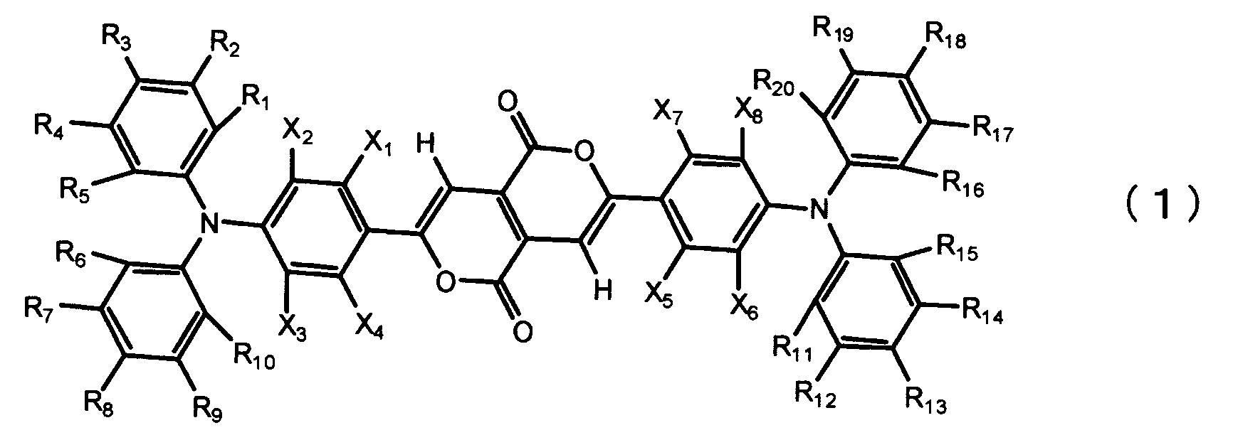
- Patent Document 1 discloses a photoelectric conversion element including a photoelectric conversion material layer having the following structural formula (1).
- the photoelectric conversion film in the photoelectric conversion element is manufactured by vapor deposition or the like, but it is desirable that a performance difference does not occur between lots of manufactured photoelectric conversion elements.
- An object of this invention is to provide a photoelectric conversion element provided with the photoelectric converting film which shows the outstanding responsiveness and manufacture aptitude in view of the said situation.
- Another object of the present invention is to provide an image sensor and a photosensor including a photoelectric conversion element.
- the present inventors have found that the above problems can be solved by using a photoelectric conversion film containing a compound having a predetermined ring structure, and have completed the present invention. That is, the above problems can be solved by the following means.
- a photoelectric conversion element having a conductive film, a photoelectric conversion film containing a photoelectric conversion material, and a transparent conductive film in this order, wherein the photoelectric conversion material is a compound represented by the general formula (1) described later Including a photoelectric conversion element.
- the photoelectric conversion material is a compound represented by the general formula (1) described later Including a photoelectric conversion element.
- a group that forms a ring may have an aryl group or a substituent that may have a substituent.
- the photoelectric conversion element according to (1) or (2) which is a good heteroaryl group.
- a 1 is a group represented by the general formula (2-1).
- (6) The photoelectric conversion device according to any one of (1) to (5), wherein in formula (1), X 1 and X 2 are both oxygen atoms.
- An optical sensor comprising the photoelectric conversion element according to any one of (1) to (10).
- (12) An imaging device comprising the photoelectric conversion device according to any one of (1) to (10).
- a photoelectric conversion element provided with the photoelectric converting film which shows the outstanding responsiveness and manufacture aptitude can be provided.
- the image pick-up element and optical sensor containing a photoelectric conversion element can be provided.
- FIG. 1A and FIG. 1B are schematic cross-sectional views each showing a configuration example of a photoelectric conversion element. It is a cross-sectional schematic diagram for 1 pixel of a hybrid type photoelectric conversion element. It is a cross-sectional schematic diagram for 1 pixel of an image pick-up element.
- a compound represented by the general formula (1) having a predetermined structure is used.
- This compound has a structure of donor part-acceptor part-donor part. That is, since it has a contrasting structure having donor portions on both sides, the dipole moment of the compound itself is relatively low, and it is difficult to trap carriers.
- the donor part contains a nitrogen atom that can stabilize the cation radical, the charge transporting property is excellent.
- the nitrogen atom of the donor part is incorporated in the ring structure, the structure is rigid and the heat resistance is improved. Excellent suitability for manufacturing conversion elements.
- FIG. 1 the cross-sectional schematic diagram of one Embodiment of the photoelectric conversion element of this invention is shown.
- a photoelectric conversion element 10a shown in FIG. 1A includes a conductive film (hereinafter also referred to as a lower electrode) 11 that functions as a lower electrode, an electron blocking film 16A formed on the lower electrode 11, and an electron blocking film 16A.
- a photoelectric conversion film 12 including a compound represented by the general formula (1), which will be described later, and a transparent conductive film 15 (hereinafter also referred to as an upper electrode) 15 that functions as an upper electrode are stacked in this order. Have a configuration.
- FIG. 1B shows a configuration example of another photoelectric conversion element.
- the photoelectric conversion element 10b shown in FIG. 1B has a configuration in which an electron blocking film 16A, a photoelectric conversion film 12, a hole blocking film 16B, and an upper electrode 15 are laminated on the lower electrode 11 in this order.
- an electron blocking film 16A, a photoelectric conversion film 12, a hole blocking film 16B, and an upper electrode 15 are laminated on the lower electrode 11 in this order.
- the stacking order of the electron blocking film 16A, the photoelectric conversion film 12, and the hole blocking film 16B in FIGS. 1A and 1B may be reversed depending on the application and characteristics. For example, the positions of the electron blocking film 16A and the photoelectric conversion film 12 may be reversed.
- the photoelectric conversion element 10 a (10 b) it is preferable that light is incident on the photoelectric conversion film 12 through the transparent conductive film 15. Moreover, when using the photoelectric conversion element 10a (10b), an electric field can be applied. In this case, it is preferable that the conductive film 11 and the transparent conductive film 15 form a pair of electrodes, and an electric field of 1 ⁇ 10 ⁇ 5 to 1 ⁇ 10 7 V / cm is applied between the pair of electrodes. From the viewpoint of performance and power consumption, an electric field of 1 ⁇ 10 ⁇ 4 to 1 ⁇ 10 6 V / cm is preferable, and an electric field of 1 ⁇ 10 ⁇ 3 to 5 ⁇ 10 5 V / cm is particularly preferable.
- FIG. 2 the cross-sectional schematic diagram of another embodiment of the photoelectric conversion element of this invention is shown.
- a photoelectric conversion element 200 illustrated in FIG. 2 represents a hybrid photoelectric conversion element including an organic photoelectric conversion film 209 and an inorganic photoelectric conversion film 201.
- the organic photoelectric conversion film 209 includes a compound represented by the general formula (1) described later.
- the inorganic photoelectric conversion film 201 has an n-type well 202, a p-type well 203, and an n-type well 204 on a p-type silicon substrate 205.
- Blue light is photoelectrically converted at the pn junction formed between the p-type well 203 and the n-type well 204 (B pixel), and the pn junction formed between the p-type well 203 and the n-type well 202 is converted into a pn junction.
- the red light is photoelectrically converted (R pixel).
- the conductivity types of the wells 202, 203, and 204 are not limited to these, and may be opposite conductivity types.
- a transparent insulating layer 207 is formed on the inorganic photoelectric conversion film 201.
- a transparent pixel electrode 208 divided for each pixel is formed on the insulating layer 207, and an organic photoelectric conversion film 209 that absorbs green light and performs photoelectric conversion is formed on the insulating layer 207 in a single configuration common to each pixel.
- an electron blocking film 212 is formed in a single configuration for each pixel sharing, on which a transparent common electrode 210 is also formed, and a transparent protective film 211 is formed on the top layer. Is formed.
- the stacking order of the electron blocking film 212 and the organic photoelectric conversion film 209 may be reverse to that shown in FIG. 2, and the common electrode 210 may be formed separately for each pixel.
- the organic photoelectric conversion film 209 constitutes a G pixel that detects green light.
- the pixel electrode 208 is the same as the lower electrode 11 of the photoelectric conversion element 10a shown in FIG.
- the common electrode 210 is the same as the upper electrode 15 of the photoelectric conversion element 10a shown in FIG.
- the mixed light of blue light and red light that has passed through the organic photoelectric conversion film 209 enters the inorganic photoelectric conversion film 201.
- Blue light having a short wavelength is photoelectrically converted mainly in the shallow part of the semiconductor substrate (inorganic photoelectric conversion film) 201 (near the pn junction formed between the p-type well 203 and the n-type well 204) to generate photocharges.
- a blue signal is output to the outside.
- Red light having a long wavelength is photoelectrically converted mainly in the deep part of the semiconductor substrate (inorganic photoelectric conversion film) 201 (near the pn junction formed between the p-type well 203 and the n-type well 202), and photocharge is generated.
- a red signal is output to the outside.
- a signal readout circuit (a charge transfer path in the case of the CCD type, a MOS transistor circuit in the case of the CMOS type) or a green signal charge is provided on the surface portion of the p-type silicon substrate 205. An accumulation region is formed. Further, the pixel electrode 208 is connected to a corresponding green signal charge storage region by a vertical wiring.
- the photoelectric conversion film 12 (or the organic photoelectric conversion film 209) is a film containing a compound represented by the following general formula (1) as a photoelectric conversion material. By using this compound, the photoelectric conversion element which has the photoelectric conversion film which shows the outstanding responsiveness and manufacturing aptitude is obtained.
- the compound represented by the general formula (1) will be described in detail.
- R 1 to R 4 each independently have an alkyl group, an aryl group that may have a substituent, a heteroaryl group that may have a substituent, or a substituent.
- an aryl group which may have a substituent in terms of more excellent responsiveness and / or manufacturability of the photoelectric conversion element hereinafter, also simply referred to as “a more excellent effect of the present invention”
- the heteroaryl group which may have a substituent is preferable, and the aryl group which may have a substituent is more preferable.
- the group contained in the group that forms a ring described later is an aryl that may have a substituent in that the effect of the present invention is more excellent. It is preferably a heteroaryl group which may have a group or a substituent. That is, for example, when R 1 and Ar 1 form a ring, R 1 is preferably an aryl group that may have a substituent or a heteroaryl group that may have a substituent.
- the number of carbon atoms in the alkyl group is not particularly limited, but 1 to 10 is preferable, 1 to 6 is more preferable, and 1 to 3 is more preferable in terms of more excellent effects of the present invention.
- the alkyl group may have a linear, branched or cyclic structure. Preferred examples of the alkyl group include a methyl group, an ethyl group, an n-propyl group, an i-propyl group, an n-butyl group, and an n-hexyl group.
- the number of carbon atoms in the aryl group is not particularly limited, but 6 to 30 is preferable and 6 to 18 is more preferable in terms of more excellent effects of the present invention.
- the aryl group may be a monocyclic structure or a condensed ring structure in which two or more rings are condensed, and may have a substituent W described later.
- Examples of the aryl group include a phenyl group, a naphthyl group, an anthryl group, a pyrenyl group, a phenanthrenyl group, a methylphenyl group, a dimethylphenyl group, a biphenyl group, and a fluorenyl group.
- a phenyl group, a naphthyl group, or an anthryl group is exemplified. preferable.
- the number of carbon atoms in the heteroaryl group is not particularly limited, but is preferably from 3 to 30, and more preferably from 3 to 18, from the viewpoint of more excellent effects of the present invention.
- the heteroaryl group may have a substituent W described later.
- the heteroaryl group includes a heteroatom other than a carbon atom and a hydrogen atom. Examples of the heteroatom include a nitrogen atom, a sulfur atom, an oxygen atom, a selenium atom, a tellurium atom, a phosphorus atom, a silicon atom, or a boron atom. And a nitrogen atom, a sulfur atom, or an oxygen atom is preferable.
- the number of heteroatoms contained in the heteroaryl group is not particularly limited and is usually about 1 to 10, and preferably 1 to 4.
- the number of ring members of the heteroaryl group is not particularly limited, but is preferably a 3- to 8-membered ring, more preferably a 5- to 7-membered ring, and particularly preferably a 5- to 6-membered ring.
- heteroaryl group examples include pyridyl group, quinolyl group, isoquinolyl group, acridinyl group, phenanthridinyl group, pteridinyl group, pyrazinyl group, quinoxalinyl group, pyrimidinyl group, quinazolinyl group, pyridazinyl group, cinnolinyl group, phthalazinyl group, Triazinyl group, oxazolyl group, benzoxazolyl group, thiazolyl group, benzothiazolyl group, imidazolyl group, benzoimidazolyl group, pyrazolyl group, indazolyl group, isoxazolyl group, benzisoxazolyl group, isothiazolyl group, benzoisothiazolyl group, oxadiazolyl Group, thiadiazolyl group, triazolyl group, tetrazolyl group, furyl group
- the number of carbon atoms in the alkenyl group is not particularly limited, but is preferably 2 to 10 and more preferably 2 to 6 from the viewpoint that the effect of the present invention is more excellent.
- the alkenyl group may have a linear, branched or cyclic structure, and may have a substituent W which will be described later.
- Preferred examples of the alkenyl group include a vinyl group and 1-propenyl group.
- substituent W includes a halogen atom, an alkyl group (including a cycloalkyl group, a bicycloalkyl group, and a tricycloalkyl group), an alkenyl group (including a cycloalkenyl group and a bicycloalkenyl group), an alkynyl group, an aryl group, and a heterocyclic ring.
- substituent W include a halogen atom, an alkyl group (including a cycloalkyl group, a bicycloalkyl group, and a tricycloalkyl group), an alkenyl group (including a cycloalkenyl group and a bicycloalkenyl group), an alkynyl group, an aryl group, and a heterocyclic ring.
- Group may be referred to as a heterocyclic group
- cyano group may be referred to as a heterocyclic group
- cyano group may be referred to as a heterocyclic group
- acyloxy group carbamoyloxy group, alkoxycarbonyloxy group
- Aryloxycarbonyloxy group amino group (including anilino group), ammonio group, acylamino group, aminocarbonylamino group, alkoxycarbonylamino group, aryloxycarbonylamino group, sulfamoylamino group, alkyl or arylsulfonylamino Group, mercapto group, alkylthio group, arylthio group, heterocyclic thio group, sulfamoyl group, sulfo group, alkyl or arylsulfinyl group, alkyl or arylsulfonyl group, acyl group, aryloxycarbony
- Ar 1 and Ar 2 each independently represent an arylene group which may have a substituent or a heteroarylene group which may have a substituent.
- the number of carbon atoms in the arylene group is not particularly limited, but 6 to 30 is preferable and 6 to 20 is more preferable in terms of more excellent effects of the present invention.
- arylene group examples include phenylene group, biphenylene group, terphenylene group, naphthylene group, anthrylene group, phenanthrylene group, pyrenediyl group, perylenediyl group, fluorenediyl group, chrysenediyl group, triphenylenediyl group, benzoanthracenediyl group, benzoic group
- phenanthrene diyl group The number of carbon atoms in the heteroarylene group is not particularly limited, but is preferably 1 to 20 and more preferably 2 to 12 in terms of more excellent effects of the present invention.
- heteroarylene group examples include a pyridylene group, a quinolylene group, an isoquinolylene group, an acridinediyl group, a phenanthridinediyl group, a pyrazinediyl group, a quinoxalinediyl group, a pyrimidinediyl group, a triazinediyl group, an imidazolediyl group, a pyrazolediyl group, Examples thereof include an oxadiazole diyl group, a triazole diyl group, a furylene group, a thienylene group, a pyrrole diyl group, an indole diyl group, and a carbazole diyl group.
- the arylene group and the heteroarylene group may have a substituent, and examples of the substituent include the substituent W.
- Ar 1 and R 1 , Ar 1 and R 2 , R 1 and R 2 , Ar 2 and R 3 , Ar 2 and R 4, and R 3 and R 4 is bonded to each other to form a ring.
- Ar 1 and R 1 , Ar 1 and R 2 , R 1 and R 2 , Ar 2 and R 3 , Ar 2 and R 4, and R 3 and R 4 are each directly or linking groups. It is preferable to form a ring by bonding via a ring, and it is more preferable to form a ring by direct bonding or a ring via an alkylene group from the viewpoint that the effect of the present invention is more excellent.
- the structure of the linking group is not particularly limited.
- An alkylene group, a silylene group, an alkenylene group, a cycloalkylene group, a cycloalkenylene group, an arylene group and the like are preferable, and an alkylene group is more preferable.
- the structure of the ring to be formed is not particularly limited, and examples thereof include an aliphatic ring that may have a hetero atom and an aromatic ring that may have a hetero atom, and the effects of the present invention are more excellent.
- An aromatic ring which may have a hetero atom is mentioned by the point.
- Ar 1 and R 1 , Ar 1 and R 2 , and R 1 and R 2 is bonded to each other to form a ring, and Ar 2 and R 1 are more effective.
- Ar 2 and R 4 and R 3 and R 4 are preferably bonded to each other to form a ring, Ar 1 and R 1 , and Ar 2 and R 3 are bonded to each other. It is more preferable to form a ring.
- a 1 represents any one group selected from the group consisting of a group represented by the general formula (2-1) to a group represented by the general formula (2-3). Among these, a group represented by the general formula (2-1) is preferable in that the effect of the present invention is more excellent.
- X 1 and X 2 each independently represent an oxygen atom, a sulfur atom, a selenium atom, ⁇ NR a1 , or ⁇ CR a2 R a3 .
- R a1 represents a hydrogen atom or a substituent.
- the substituent include the above-described substituent W, and among them, an alkyl group or an aryl group is preferable in that the effect of the present invention is more excellent.
- R a2 and R a3 each independently represent a cyano group, a carbonyl group or an alkoxycarbonyl group.
- Y 1 and Y 2 each independently represent an oxygen atom, a sulfur atom, a selenium atom,> NR b1 ,> CR b2 R b3 , or> SiR b4 R b5 .
- an oxygen atom or a sulfur atom is preferable at the point which the effect of this invention is more excellent, and an oxygen atom is more preferable.
- R b1 to R b5 each independently represents a hydrogen atom or a substituent. Examples of the substituent include the above-described substituent W, and among them, an alkyl group is preferable in that the effect of the present invention is more excellent.
- * 1 and * 2 represent that they are bonded to * 1 and * 2 in the general formulas (2-1) to (2-3), respectively. More specifically, examples of structural formulas in the case where the groups represented by the general formulas (2-1) to (2-3) are introduced into A 1 in the general formula (1) are shown below.
- R 11 to R 14 , R 21 to R 25 , R 31 to R 35 , R 41 to R 44 , R 51 to R 55 , and R 61 to R 65 are each independently Represents a hydrogen atom or a substituent.
- the substituent W mentioned above is mentioned, for example.
- At least one of R 12 and R 21 , R 25 and R 31 , R 13 and R 35 , R 42 and R 51 , R 55 and R 61 , and R 43 and R 65 is bonded to each other. To form a ring.
- the definition of A 1 is as described above.
- the dipole moment of the compound represented by the general formula (1) is not particularly limited, 1D or less is preferable and 0.5D or less is more preferable in that the effect of the present invention is more excellent.
- the dipole moment can be obtained by calculation. Specifically, it can be obtained by molecular orbital calculation software Gaussian 09 (manufactured by Gaussian) using the basis function 6-31G (d) in the B3LYP method.
- the compound represented by the general formula (1) preferably has an absorption maximum at 400 nm or more and less than 720 nm in the ultraviolet-visible absorption spectrum.
- the peak wavelength (absorption maximum wavelength) of the absorption spectrum is more preferably 450 nm or more and 700 nm or less, more preferably 480 nm or more and 650 nm or less from the viewpoint of absorbing mainly light in the visible region, particularly light in the G region (500 to 600 nm). Is more preferable, and it is particularly preferably 500 nm or more and 600 nm or less.
- the absorption maximum wavelength of the compound represented by the general formula (1) can be measured using a UV solution of Shimadzu Corporation with a chloroform solution of the compound.
- Concentration of the chloroform solution is preferably from 5 ⁇ 10 -5 ⁇ 1 ⁇ 10 -7 mol / l, more preferably 3 ⁇ 10 -5 ⁇ 2 ⁇ 10 -6 mol / l, 2 ⁇ 10 -5 ⁇ 5 ⁇ 10 - 6 mol / l is particularly preferred.
- the compound represented by the general formula (1) has an absorption maximum at 400 nm or more and less than 720 nm in the ultraviolet-visible absorption spectrum, and the molar extinction coefficient at the absorption maximum wavelength is 10,000 mol ⁇ 1 ⁇ l ⁇ cm ⁇ 1 or more. Is preferred. In order to reduce the film thickness of the photoelectric conversion film and obtain an element having high charge collection efficiency, high-speed response, and high sensitivity characteristics, a material having a large molar extinction coefficient is preferable. More preferably 30000mol -1 ⁇ l ⁇ cm -1 or more as a molar extinction coefficient of the compound represented by the general formula (1), more preferably 50000mol -1 ⁇ l ⁇ cm -1 or more. The molar extinction coefficient of the compound represented by the general formula (1) is measured with a chloroform solution.
- the compound represented by the general formula (1) is less likely to be decomposed during vapor deposition as the difference between the melting point and the vapor deposition temperature (melting point ⁇ vapor deposition temperature) is increased, and the vapor deposition rate can be increased by applying a higher temperature.
- the difference between the melting point and the deposition temperature (melting point ⁇ deposition temperature) is preferably 30 ° C. or higher, more preferably 45 ° C. or higher, and still more preferably 60 ° C. or higher.
- the molecular weight of the compound represented by the general formula (1) is preferably from 300 to 1500, more preferably from 500 to 1000, and particularly preferably from 500 to less than 850, from the viewpoint that the effect of the present invention is more excellent.
- the molecular weight of the compound is 1500 or less, the deposition temperature does not increase and the compound is hardly decomposed. If the molecular weight of the compound is 300 or more, the glass transition point of the deposited film is not lowered, and the heat resistance of the device is hardly lowered.
- the glass transition point (Tg) of the compound represented by the general formula (1) is preferably 95 ° C. or higher, more preferably 110 ° C. or higher, further preferably 135 ° C. or higher, particularly preferably 150 ° C. or higher, and 160 ° C. or higher. Most preferred. A high glass transition point is preferable because the heat resistance of the device is improved.
- the compound represented by the general formula (1) is particularly useful as a material for a photoelectric conversion film used for an image sensor, a photosensor, or a photovoltaic cell.
- the compound represented by the general formula (1) functions as an organic p-type compound in the photoelectric conversion film.
- it can also be used as a coloring material, liquid crystal material, organic semiconductor material, organic light emitting device material, charge transport material, pharmaceutical material, fluorescent diagnostic material, and the like.
- the photoelectric conversion film may further contain a photoelectric conversion material of an organic p-type compound or an organic n-type compound.
- An organic p-type compound is a donor-type organic semiconductor (compound), which is mainly represented by a hole-transporting organic compound and refers to an organic compound having a property of easily donating electrons. More specifically, an organic compound having a smaller ionization potential when two organic materials are used in contact with each other. Therefore, any organic compound can be used as the donor organic compound as long as it is an electron-donating organic compound.
- a triarylamine compound a benzidine compound, a pyrazoline compound, a styrylamine compound, a hydrazone compound, a triphenylmethane compound, a carbazole compound, or the like can be used.
- organic n-type compound is an acceptor organic semiconductor, which is represented by an organic compound having an electron transport property and has a property of easily accepting electrons. More specifically, the organic compound having the higher electron affinity when two organic compounds are used in contact with each other. Therefore, any organic compound may be used as the acceptor organic semiconductor as long as it is an organic compound having an electron accepting property.
- fullerene or fullerene derivatives condensed aromatic carbocyclic compounds (naphthalene derivatives, anthracene derivatives, phenanthrene derivatives, tetracene derivatives, pyrene derivatives, perylene derivatives, fluoranthene derivatives), nitrogen atoms, oxygen atoms, sulfur atoms containing 5 to 5 7-membered heterocyclic compounds (eg, pyridine, pyrazine, pyrimidine, pyridazine, triazine, quinoline, quinoxaline, quinazoline, phthalazine, cinnoline, isoquinoline, pteridine, acridine, phenazine, phenanthroline, tetrazole, pyrazole, imidazole, thiazole, oxazole, indazole , Benzimidazole, benzotriazole, benzoxazole, benzothiazole, carb
- fullerenes selected from the group consisting of fullerenes and fullerene derivatives are preferred when used in an embodiment as shown in FIG.
- the fullerene, fullerene C 60, fullerene C 70, fullerene C 76, fullerene C 78, fullerene C 80, fullerene C 82, fullerene C 84, fullerene C 90, fullerene C 96, fullerene C 240, fullerene C 540, mixed Fullerene is represented, and the fullerene derivative represents a compound having a substituent added thereto.
- the substituent an alkyl group, an aryl group, or a heterocyclic group is preferable.
- the fullerene derivative compounds described in JP-A-2007-123707 are preferred.
- the organic n-type compound when used in an embodiment as shown in FIG. 2, it is desirable that the organic n-type compound is colorless or has an absorption maximum wavelength and / or absorption waveform close to that of the organic p-type compound. It is desirable that the absorption maximum wavelength is 400 nm or less, or 500 nm or more and 600 nm or less. Any compound can be used as long as it has the characteristics of the organic n-type compound described above and is suitable for absorption, such as the compounds described in [0016] to [0019] of US2013-0112947. .
- the photoelectric conversion film preferably has a bulk heterostructure formed by mixing the compound represented by the general formula (1) and the organic n-type compound.
- a bulk heterostructure is a layer in which an organic p-type compound and an organic n-type compound are mixed and dispersed in a photoelectric conversion film, and can be formed by either a wet method or a dry method, but is preferably formed by a co-evaporation method. .
- the heterojunction structure it is possible to make up for the disadvantage that the carrier diffusion length of the photoelectric conversion film is short, and to improve the photoelectric conversion efficiency of the photoelectric conversion film.
- the bulk heterojunction structure is described in detail in JP-A-2005-303266, [0013] to [0014].
- the film thickness of the compound represented by the general formula (1) + the film thickness in terms of a single layer + the film thickness in terms of a single layer of the organic n-type compound)) is a case where the organic n-type compound is a fullerene It is preferably 50% by volume or more, more preferably 55% by volume or more, and further preferably 65% by volume or more.
- the upper limit is not particularly limited, but is preferably 95% by volume or less, and more preferably 90% by volume or less.
- the content is preferably 20% by volume to 80% by volume, more preferably 30% by volume to 70% by volume, More preferably, it is 40 volume% or more and 60 volume% or less.
- the photoelectric conversion film containing the compound represented by the general formula (1) and the organic n-type compound of the present invention is a non-light-emitting film and has characteristics different from those of an organic electroluminescent element (OLED).
- the non-light-emitting film is a film having an emission quantum efficiency of 1% or less, more preferably 0.5% or less, and still more preferably 0.1% or less.
- the photoelectric conversion film can be mainly formed by a dry film forming method.
- the dry film forming method include a vapor deposition method (particularly, a vacuum vapor deposition method), a sputtering method, a physical vapor deposition method such as an ion plating method, an MBE method, or a CVD method such as plasma polymerization.
- the vacuum evaporation method is preferable.
- manufacturing conditions such as the degree of vacuum and the evaporation temperature can be set according to a conventional method.
- the thickness of the photoelectric conversion film is preferably 10 nm to 1000 nm, more preferably 50 nm to 800 nm, and particularly preferably 100 nm to 500 nm. By setting it to 10 nm or more, a suitable dark current suppressing effect is obtained, and by setting it to 1000 nm or less, suitable photoelectric conversion efficiency is obtained.
- the electrodes are made of a conductive material.
- a metal, an alloy, a metal oxide, an electrically conductive compound, or a mixture thereof can be used. Since light is incident from the upper electrode 15, it is preferable that the upper electrode 15 is sufficiently transparent to the light to be detected.
- conductive metal oxides such as tin oxide (ATO, FTO) doped with antimony or fluorine, tin oxide, zinc oxide, indium oxide, indium tin oxide (ITO), indium zinc oxide (IZO), Metal thin films such as gold, silver, chromium, nickel, etc., and mixtures or laminates of these metals and conductive metal oxides, inorganic conductive materials such as copper iodide and copper sulfide, organics such as polyaniline, polythiophene, and polypyrrole Examples thereof include conductive materials and laminates of these with ITO. Among these, a transparent conductive metal oxide is preferable from the viewpoint of high conductivity and transparency.
- the sheet resistance is preferably 100 to 10,000 ⁇ / ⁇ .
- the thickness of the upper electrode (transparent conductive film) 15 decreases, the amount of light absorbed decreases, and the light transmittance generally increases. The increase in light transmittance is very preferable because it increases the light absorption in the photoelectric conversion film and increases the photoelectric conversion ability.
- the thickness of the upper electrode 15 is preferably 5 to 100 nm, and more preferably 5 to 20 nm. It is desirable.
- the lower electrode 11 may have transparency, or conversely, may use a material that does not have transparency and reflects light.
- conductive metal oxides such as tin oxide (ATO, FTO) doped with antimony or fluorine, tin oxide, zinc oxide, indium oxide, indium tin oxide (ITO), indium zinc oxide (IZO), Metals such as gold, silver, chromium, nickel, titanium, tungsten, and aluminum, and conductive compounds such as oxides and nitrides of these metals (for example, titanium nitride (TiN)), and these metals and conductivity Examples include mixtures or laminates with metal oxides, inorganic conductive materials such as copper iodide and copper sulfide, organic conductive materials such as polyaniline, polythiophene, and polypyrrole, and laminates of these with ITO or titanium nitride. .
- the method for forming the electrode is not particularly limited, and can be appropriately selected depending on the electrode material. Specifically, it can be formed by a wet method such as a printing method or a coating method, a physical method such as a vacuum deposition method, a sputtering method, or an ion plating method, or a chemical method such as CVD or plasma CVD method.
- the electrode material is ITO, it can be formed by a method such as an electron beam method, a sputtering method, a resistance heating vapor deposition method, a chemical reaction method (such as a sol-gel method), or a dispersion of indium tin oxide.
- UV-ozone treatment, plasma treatment, or the like can be performed on a film formed using ITO.
- various methods including a reactive sputtering method can be used, and further, UV-ozone treatment, plasma treatment, and the like can be performed.
- the photoelectric conversion element of the present invention may have a charge blocking film. By having this film, the characteristics (photoelectric conversion efficiency, response speed, etc.) of the obtained photoelectric conversion element are more excellent.
- Examples of the charge blocking film include an electron blocking film and a hole blocking film. Below, each film
- An electron donating organic material can be used for the electron blocking film.
- JP-A-2008-72090 Polymers such as phenylene vinylene, fluorene, carbazole, indole, pyrene, pyrrole, picoline, thiophene, acetylene, diacetylene, etc., and derivatives thereof can be used even if they are not electron donating compounds.
- [0083] to [0089] of JP-A-2008-72090 and [0043] to [0063 of JP-A-2011-176259 are usable.
- [0121] to [0148] of JP2011-228614A, and [0108] to [0156] of JP2011-228615A are preferable.
- the electron blocking film may be composed of a plurality of films.
- An inorganic material can also be used as the electron blocking film.
- Materials that can be used as electron blocking films include calcium oxide, chromium oxide, chromium copper oxide, manganese oxide, cobalt oxide, nickel oxide, copper oxide, gallium copper oxide, strontium copper oxide, niobium oxide, molybdenum oxide, indium copper oxide, and oxide. Examples include indium silver and iridium oxide.
- the layer can be a layer made of an inorganic material, or in the case of a plurality of layers, one or more layers can be a layer made of an inorganic material. .
- An electron-accepting organic material can be used for the hole blocking film.
- electron-accepting materials include 1,3-bis (4-tert-butylphenyl-1,3,4-oxadiazolyl) phenylene (OXD-7) and other oxadiazole derivatives, anthraquinodimethane derivatives, and diphenylquinone derivatives.
- a porphyrin compound or a styryl compound such as DCM (4-dicyanomethylene-2-methyl-6- (4- (dimethylaminostyryl))-4H pyran) or a 4H pyran compound can be used.
- DCM dimethylaminostyryl
- a 4H pyran compound can be used.
- compounds described in [0073] to [0078] of JP-A-2008-72090 are preferable.
- the method for producing the charge blocking film is not particularly limited, and the film can be formed by a dry film forming method or a wet film forming method.
- a dry film forming method a vapor deposition method, a sputtering method, or the like can be used.
- the vapor deposition may be either physical vapor deposition (PVD) or chemical vapor deposition (CVD), but physical vapor deposition such as vacuum vapor deposition is preferred.
- PVD physical vapor deposition
- CVD chemical vapor deposition
- the wet film forming method an inkjet method, a spray method, a nozzle printing method, a spin coating method, a dip coating method, a casting method, a die coating method, a roll coating method, a bar coating method, a gravure coating method, etc. can be used. From the viewpoint of high-precision patterning, the inkjet method is preferable.
- the thickness of the charge blocking film is preferably 10 to 200 nm, more preferably 30 to 150 nm, and particularly preferably 50 to 100 nm. This is because if the thickness is too thin, the dark current suppressing effect is lowered, and if it is too thick, the photoelectric conversion efficiency is lowered.
- the photoelectric conversion element may further include a substrate.
- the type of the substrate used is not particularly limited, and a semiconductor substrate, a glass substrate, or a plastic substrate can be used.
- the position of the substrate is not particularly limited, but usually a conductive film, a photoelectric conversion film, and a transparent conductive film are laminated on the substrate in this order.
- the photoelectric conversion element may further include a sealing layer.
- the performance of photoelectric conversion materials may deteriorate significantly due to the presence of degradation factors such as water molecules. Ceramics such as dense metal oxides, metal nitrides, and metal nitride oxides that do not penetrate water molecules and diamond-like materials Covering and sealing the entire photoelectric conversion film with a sealing layer such as carbon (DLC) can prevent the deterioration.
- the material for the sealing layer may be selected and manufactured according to paragraphs [0210] to [0215] of JP2011-082508A.
- the photoelectric conversion element of the present invention is preferably used as an optical sensor.
- the photoelectric conversion element used alone may be used, or a line sensor in which the photoelectric conversion elements are linearly arranged or a two-dimensional sensor arranged on a plane is preferable.
- the photoelectric conversion element of the present invention converts optical image information into an electrical signal using an optical system and a drive unit like a scanner in a line sensor, and optically converts optical image information like an imaging module in a two-dimensional sensor.
- the system functions as an image sensor by forming an image on a sensor and converting it into an electrical signal.
- the photovoltaic cell is a power generation device, the efficiency of converting light energy into electrical energy is an important performance, but dark current, which is a current in a dark place, is not a functional problem. Further, a subsequent heating step such as installation of a color filter is not necessary. Since it is important to convert light and dark signals into electrical signals with high accuracy, the efficiency of converting light intensity into current is also important for optical sensors. Low dark current is required.
- An image sensor is an element that converts optical information of an image into an electric signal.
- a plurality of photoelectric conversion elements are arranged on a matrix in the same plane, and an optical signal is converted into an electric signal in each photoelectric conversion element (pixel). That can be output to the outside of the imaging device for each pixel sequentially. Therefore, one pixel is composed of one photoelectric conversion element and one or more transistors.
- FIG. 3 is a schematic cross-sectional view showing a schematic configuration of an image sensor for explaining an embodiment of the present invention.
- This imaging device is used by being mounted on an imaging device such as a digital camera or a digital video camera, an imaging module such as an electronic endoscope or a mobile phone, or the like.
- This imaging element has a plurality of photoelectric conversion elements having the configuration shown in FIG. 1 and a circuit board on which a readout circuit for reading a signal corresponding to the charge generated in the photoelectric conversion film of each photoelectric conversion element is formed.
- a plurality of photoelectric conversion elements are arranged one-dimensionally or two-dimensionally on the same surface above the circuit board.
- connection electrode 103 includes a connection electrode 103, a pixel electrode (lower electrode) 104, a connection portion 105, a connection portion 106, a photoelectric conversion film 107, and a counter electrode.
- the pixel electrode 104 has the same function as the lower electrode 11 of the photoelectric conversion element 10a shown in FIG.
- the counter electrode 108 has the same function as the upper electrode 15 of the photoelectric conversion element 10a shown in FIG.
- the photoelectric conversion film 107 has the same configuration as the layer provided between the lower electrode 11 and the upper electrode 15 of the photoelectric conversion element 10a illustrated in FIG.
- the substrate 101 is a glass substrate or a semiconductor substrate such as Si.
- An insulating layer 102 is formed on the substrate 101.
- a plurality of pixel electrodes 104 and a plurality of connection electrodes 103 are formed on the surface of the insulating layer 102.
- the photoelectric conversion film 107 is a layer common to all the photoelectric conversion elements provided on the plurality of pixel electrodes 104 so as to cover them.
- the counter electrode 108 is one electrode provided on the photoelectric conversion film 107 and common to all the photoelectric conversion elements.
- the counter electrode 108 is formed up to the connection electrode 103 disposed outside the photoelectric conversion film 107, and is electrically connected to the connection electrode 103.
- connection part 106 is embedded in the insulating layer 102 and is a plug or the like for electrically connecting the connection electrode 103 and the counter electrode voltage supply part 115.
- the counter electrode voltage supply unit 115 is formed on the substrate 101 and applies a predetermined voltage to the counter electrode 108 via the connection unit 106 and the connection electrode 103.
- the power supply voltage is boosted by a booster circuit such as a charge pump to supply the predetermined voltage.
- the readout circuit 116 is provided on the substrate 101 corresponding to each of the plurality of pixel electrodes 104, and reads out a signal corresponding to the charge collected by the corresponding pixel electrode 104.
- the readout circuit 116 is configured by, for example, a CCD, a CMOS circuit, a TFT circuit, or the like, and is shielded from light by a light shielding layer (not shown) disposed in the insulating layer 102.
- the readout circuit 116 is electrically connected to the corresponding pixel electrode 104 via the connection unit 105.
- the buffer layer 109 is formed on the counter electrode 108 so as to cover the counter electrode 108.
- the sealing layer 110 is formed on the buffer layer 109 so as to cover the buffer layer 109.
- the color filter 111 is formed at a position facing each pixel electrode 104 on the sealing layer 110.
- the partition wall 112 is provided between the color filters 111 and is for improving the light transmission efficiency of the color filter 111.
- the light shielding layer 113 is formed in a region other than the region where the color filter 111 and the partition 112 on the sealing layer 110 are provided, and prevents light from entering the photoelectric conversion film 107 formed outside the effective pixel region.
- the protective layer 114 is formed on the color filter 111, the partition 112, and the light shielding layer 113, and protects the entire image sensor 100.
- the imaging device 100 when light is incident, the light is incident on the photoelectric conversion film 107, and charges are generated here. Holes in the generated charges are collected by the pixel electrode 104, and a voltage signal corresponding to the amount is output to the outside of the image sensor 100 by the readout circuit 116.
- the manufacturing method of the image sensor 100 is as follows. On the circuit board on which the common electrode voltage supply unit 115 and the readout circuit 116 are formed, the connection units 105 and 106, the plurality of connection electrodes 103, the plurality of pixel electrodes 104, and the insulating layer 102 are formed. The plurality of pixel electrodes 104 are arranged on the surface of the insulating layer 102 in a square lattice pattern, for example.
- a photoelectric conversion film 107 is formed on the plurality of pixel electrodes 104 by, for example, a vacuum heating deposition method.
- the counter electrode 108 is formed on the photoelectric conversion film 107 under vacuum by, for example, sputtering.
- the buffer layer 109 and the sealing layer 110 are sequentially formed on the counter electrode 108 by, for example, a vacuum heating deposition method.
- the protective layer 114 is formed, and the imaging element 100 is completed.
- Compound D-2, Compound D-4, Compound D-5, Compound D-7, Compound D-11, Compound D-15 to Compound D-17, Compound D- used in Examples and Comparative Examples described later 20, Compound D-24, Compound D-30, Compound D-31, Compound D-40, Compound D-43, Compound D-53, Compound D-56, Compound RD-1, and Compound RD-2 are the above compounds.
- the synthesis was carried out with reference to the synthesis method of D-1 and known methods.
- the number of the said compound corresponds to the example number of the compound represented by General formula (1) mentioned above.
- the compounds used in the examples and comparative examples are collectively shown below.
- the photoelectric conversion element in the form of FIG. includes the lower electrode 11, the electron blocking film 16 ⁇ / b> A, the photoelectric conversion film 12, and the upper electrode 15.
- an amorphous ITO film is formed on a glass substrate by sputtering to form the lower electrode 11 (thickness: 30 nm), and the following compound (EB-1) is heated on the lower electrode 11 by vacuum heating.
- An electron blocking film 16A was formed by vapor deposition.
- the above compound D-1 and fullerene (C 60 ) are deposited on the electron blocking film 16A by vacuum heating deposition so that the single layer equivalent is 120 nm and 280 nm, respectively.
- the photoelectric conversion film 12 was formed by co-evaporation to form a film. Further, an amorphous ITO film was formed on the photoelectric conversion film 12 by sputtering to form an upper electrode 15 (transparent conductive film) (thickness: 10 nm). An SiO film was formed as a sealing layer on the upper electrode 15 by heating vapor deposition, and then an aluminum oxide (Al 2 O 3 ) layer was formed thereon by ALCVD to produce a photoelectric conversion element. Each photoelectric conversion element was produced according to the same procedure as described above except that the compounds shown in Table 1 described later were used instead of the compound D-1. The evaluation results correspond to Table 1.
- ⁇ Preparation 2 of photoelectric conversion element (element assuming the embodiment of FIG. 2)>
- the photoelectric conversion element includes the lower electrode 11, the electron blocking film 16 ⁇ / b> A, the photoelectric conversion film 12, and the upper electrode 15.
- an amorphous ITO film is formed on a glass substrate by sputtering to form the lower electrode 11 (thickness: 30 nm), and the above compound (EB-1) is vacuum-heated on the lower electrode 11
- An electron blocking film 16A (thickness: 100 nm) was formed by vapor deposition.
- the above compound D-1 and the following compound N-1 are vacuum heated and evaporated on the electron blocking film 16A so as to be 100 nm and 100 nm, respectively, in terms of a single layer.
- the photoelectric conversion film 12 was formed by co-evaporation to form a film. Further, an amorphous ITO film was formed on the photoelectric conversion film 12 by sputtering to form an upper electrode 15 (transparent conductive film) (thickness: 10 nm). An SiO film was formed as a sealing layer on the upper electrode 15 by heating vapor deposition, and then an aluminum oxide (Al 2 O 3 ) layer was formed thereon by ALCVD to produce a photoelectric conversion element. Each photoelectric conversion element was produced according to the same procedure as described above except that the compounds shown in Table 2 described later were used instead of the compound D-1. The evaluation results correspond to Table 2.
- ⁇ Response speed evaluation (response evaluation)> Responsiveness was evaluated for each obtained photoelectric conversion element. Specifically, a voltage was applied to the photoelectric conversion element so that the electric field strength was 2.0 ⁇ 10 5 V / cm. After that, the LED is turned on instantaneously, light is irradiated from the upper electrode (transparent conductive film) side, the photocurrent at that time is measured with an oscilloscope, and the relative response speed (rise from 0 to 98% signal intensity) Time). In the measurement of the response speed of each element, light was incident from the upper electrode (transparent conductive film) side. The method for obtaining the response speed (relative value) is shown below.
- the response speed (relative value) of Example X (or Comparative Example X) [from 0 to 98% signal intensity in Example X (or Comparative Example X) Rise time / rise time from 0 to 98% signal intensity in Example 1].
- the response speed (relative value) of Example X (or Comparative Example X) [from 0 to 98% signal strength in Example X (or Comparative Example X) Rise time / rise time from 0 to 98% signal strength in Example 18].
- said response speed (relative value) it is preferable that it is 15 or less practically, it is more preferable that it is 5 or less, and it is further more preferable that it is 2 or less.
- the rise time from 0 to 98% signal intensity was evaluated according to the same procedure as the evaluation of responsiveness described above for each of the “elements produced immediately after the start of vapor deposition” and “elements produced after 5 hours from the start of vapor deposition”.
- molecular weight indicates the molecular weight of the photoelectric conversion material used in each example and comparative example.
- dipole moment indicates the dipole moment of the photoelectric conversion material used in each example and comparative example.
- the photoelectric conversion element of the present invention exhibits excellent responsiveness and manufacturing suitability.
- Example 1 Example 13 and Example 14
- both X 1 and X 2 are oxygen atoms
- the responsiveness is more excellent.
- Example 5 and Example 15 it was confirmed that when the group represented by the general formula (2-1) was used, the responsiveness was more excellent.
- Example 5 and Example 8 when Ar 1 and R 1 , and Ar 2 and R 3 are bonded to each other to form a ring, responsiveness and production suitability are further improved. It was confirmed to be excellent.
- a group that forms a ring among R 1 , R 2 , R 3 , and R 4 may be an aryl group that may have a substituent or In the case of a heteroaryl group which may have a substituent, it was confirmed that the responsiveness and the production suitability were more excellent.
- An image sensor similar to that shown in FIG. 3 was produced. That is, after depositing amorphous TiN 30 nm on the CMOS substrate by sputtering, patterning is performed by photolithography so that one pixel exists on each photodiode (PD) on the CMOS substrate to form the lower electrode. After film formation of the electron blocking material, it was produced in the same manner as in Examples 1 to 17 and Comparative Examples 1 and 2. The evaluation was performed in the same manner, and the same results as in Table 1 were obtained. It was found that the imaging element was suitable for manufacturing and showed excellent performance.
Landscapes
- Physics & Mathematics (AREA)
- Spectroscopy & Molecular Physics (AREA)
- Chemical & Material Sciences (AREA)
- Engineering & Computer Science (AREA)
- Materials Engineering (AREA)
- Light Receiving Elements (AREA)
- Solid State Image Pick-Up Elements (AREA)
- Electroluminescent Light Sources (AREA)
Abstract
本発明は、優れた応答性および製造適性を示す、光電変換膜を備える光電変換素子、並びに、この素子を含む撮像素子および光センサを提供する。本発明の光電変換素子は、導電性膜、光電変換材料を含む光電変換膜、および透明導電性膜をこの順で積層してなる光電変換素子であって、光電変換材料が、一般式(1)で表される化合物を含む。
Description
本発明は、光電変換素子、撮像素子、光センサに関する。
従来の光センサは、シリコン(Si)などの半導体基板中にフォトダイオード(PD)を形成した素子であり、固体撮像素子としては、PDを2次元的に配列し、各PDで発生した信号電荷を回路で読み出す平面型固体撮像素子が広く用いられている。
カラー固体撮像素子を実現するには、平面型固体撮像素子の光入射面側に、特定の波長の光を透過するカラーフィルタを配した構造が一般的である。現在、デジタルカメラなどに広く用いられている2次元的に配列した各PD上に、青色(B)光、緑色(G)光、赤色(R)光を透過するカラーフィルタを規則的に配した単板式固体撮像素子がよく知られている。
この単板式固体撮像素子においては、カラーフィルタを透過しなかった光が利用されず光利用効率が悪い。近年、多画素化が進む中、画素サイズが小さくなっており、開口率の低下、集光効率の低下が問題になっている。
カラー固体撮像素子を実現するには、平面型固体撮像素子の光入射面側に、特定の波長の光を透過するカラーフィルタを配した構造が一般的である。現在、デジタルカメラなどに広く用いられている2次元的に配列した各PD上に、青色(B)光、緑色(G)光、赤色(R)光を透過するカラーフィルタを規則的に配した単板式固体撮像素子がよく知られている。
この単板式固体撮像素子においては、カラーフィルタを透過しなかった光が利用されず光利用効率が悪い。近年、多画素化が進む中、画素サイズが小さくなっており、開口率の低下、集光効率の低下が問題になっている。
これらの欠点を解決するため、アモルファスシリコンによる光電変換膜やその他の光電変換材料を用いた光電変換膜を信号読出し用基板上に形成する構造が知られている。
光電変換膜を用いた光電変換素子については幾つかの公知例がある。
例えば、特許文献1では、以下の構造式(1)からなる光電変換材料層を備える光電変換素子が開示されている。
光電変換膜を用いた光電変換素子については幾つかの公知例がある。
例えば、特許文献1では、以下の構造式(1)からなる光電変換材料層を備える光電変換素子が開示されている。
近年、撮像素子や光センサなどの性能向上の要求に伴い、これらに使用される光電変換膜に求められる応答速度などの諸特性に関しても、その向上が求められている。
また、光電変換素子が使用される各種デバイスの低コスト化の要求に伴い、光電変換素子をより生産性良く製造することが重要となっている。一般的に、光電変換素子中の光電変換膜は蒸着などにより製造されるが、製造される光電変換素子のロット間において性能差が生じないことが望ましい。つまり、光電変換膜を蒸着プロセスにより形成する製造ラインにおいて、一旦、光電変換材料を蒸着装置中のるつぼに入れて連続蒸着を行う際に、製造初期に製造された光電変換素子と、製造後期に製造された光電変換素子とで、応答速度に差がないこと、つまり、製造適性に優れる光電変換素子が望ましい。
本発明者らは、特許文献1に開示されている化合物を使用して光電変換素子の作製を行ったところ、得られた光電変換素子の応答速度、および、製造適性の点において必ずしも昨今求められるレベルに達しておらず、さらなる向上が必要であることを見出した。
また、光電変換素子が使用される各種デバイスの低コスト化の要求に伴い、光電変換素子をより生産性良く製造することが重要となっている。一般的に、光電変換素子中の光電変換膜は蒸着などにより製造されるが、製造される光電変換素子のロット間において性能差が生じないことが望ましい。つまり、光電変換膜を蒸着プロセスにより形成する製造ラインにおいて、一旦、光電変換材料を蒸着装置中のるつぼに入れて連続蒸着を行う際に、製造初期に製造された光電変換素子と、製造後期に製造された光電変換素子とで、応答速度に差がないこと、つまり、製造適性に優れる光電変換素子が望ましい。
本発明者らは、特許文献1に開示されている化合物を使用して光電変換素子の作製を行ったところ、得られた光電変換素子の応答速度、および、製造適性の点において必ずしも昨今求められるレベルに達しておらず、さらなる向上が必要であることを見出した。
本発明は、上記実情に鑑みて、優れた応答性および製造適性を示す、光電変換膜を備える光電変換素子を提供することを目的とする。
また、本発明は、光電変換素子を含む撮像素子および光センサを提供することも目的とする。
また、本発明は、光電変換素子を含む撮像素子および光センサを提供することも目的とする。
本発明者らは、上記課題について鋭意検討した結果、所定の環構造を有する化合物を含む光電変換膜を使用することにより上記課題を解決できることを見出し、本発明を完成するに至った。
すなわち、以下に示す手段により上記課題を解決し得る。
すなわち、以下に示す手段により上記課題を解決し得る。
(1) 導電性膜、光電変換材料を含む光電変換膜、および透明導電性膜をこの順で有する光電変換素子であって、光電変換材料が、後述する一般式(1)で表される化合物を含む、光電変換素子。
(2) 一般式(1)中、Ar1とR1、Ar1とR2およびR1とR2の少なくとも一つ、並びに、Ar2とR3、Ar2とR4およびR3とR4の少なくとも一つがそれぞれ互いに結合して環を形成する、(1)に記載の光電変換素子。
(3) 一般式(1)中、R1、R2、R3、および、R4のうち環を形成する基が、置換基を有してもよいアリール基または置換基を有してもよいヘテロアリール基である、(1)または(2)に記載の光電変換素子。
(4) 一般式(1)中、Ar1とR1、および、Ar2とR3が、それぞれ互いに結合して環を形成する、(1)~(3)のいずれかに記載の光電変換素子。
(5) A1が一般式(2-1)で表される基である、(1)~(4)のいずれかに記載の光電変換素子。
(6) 一般式(1)中、X1およびX2がいずれも酸素原子である、(1)~(5)のいずれかに記載の光電変換素子。
(7) 一般式(1)で表される化合物の双極子モーメントが1D以下である、(1)~(6)のいずれかに記載の光電変換素子。
(8) 一般式(1)で表される化合物の分子量が500以上850未満である、(1)~(7)のいずれかに記載の光電変換素子。
(9) 光電変換膜が、さらに有機n型化合物を含む、(1)~(8)のいずれかに記載の光電変換素子。
(10) 導電性膜と透明導電性膜との間に電荷ブロッキング膜が配置される、(1)~(9)のいずれかに記載の光電変換素子。
(11) (1)~(10)のいずれかに記載の光電変換素子を含む光センサ。
(12) (1)~(10)のいずれかに記載の光電変換素子を含む撮像素子。
(2) 一般式(1)中、Ar1とR1、Ar1とR2およびR1とR2の少なくとも一つ、並びに、Ar2とR3、Ar2とR4およびR3とR4の少なくとも一つがそれぞれ互いに結合して環を形成する、(1)に記載の光電変換素子。
(3) 一般式(1)中、R1、R2、R3、および、R4のうち環を形成する基が、置換基を有してもよいアリール基または置換基を有してもよいヘテロアリール基である、(1)または(2)に記載の光電変換素子。
(4) 一般式(1)中、Ar1とR1、および、Ar2とR3が、それぞれ互いに結合して環を形成する、(1)~(3)のいずれかに記載の光電変換素子。
(5) A1が一般式(2-1)で表される基である、(1)~(4)のいずれかに記載の光電変換素子。
(6) 一般式(1)中、X1およびX2がいずれも酸素原子である、(1)~(5)のいずれかに記載の光電変換素子。
(7) 一般式(1)で表される化合物の双極子モーメントが1D以下である、(1)~(6)のいずれかに記載の光電変換素子。
(8) 一般式(1)で表される化合物の分子量が500以上850未満である、(1)~(7)のいずれかに記載の光電変換素子。
(9) 光電変換膜が、さらに有機n型化合物を含む、(1)~(8)のいずれかに記載の光電変換素子。
(10) 導電性膜と透明導電性膜との間に電荷ブロッキング膜が配置される、(1)~(9)のいずれかに記載の光電変換素子。
(11) (1)~(10)のいずれかに記載の光電変換素子を含む光センサ。
(12) (1)~(10)のいずれかに記載の光電変換素子を含む撮像素子。
本発明によれば、優れた応答性および製造適性を示す、光電変換膜を備える光電変換素子を提供することができる。
また、本発明によれば、光電変換素子を含む撮像素子および光センサを提供することができる。
また、本発明によれば、光電変換素子を含む撮像素子および光センサを提供することができる。
以下に、本発明の光電変換素子の好適実施態様について説明する。
本発明の従来技術と比較した特徴点の一つとしては、所定の構造を有する一般式(1)で表される化合物を使用している点が挙げられる。この化合物は、ドナー部-アクセプター部-ドナー部の構造を有する。つまり、ドナー部を両側に有する対照的な構造を有するため、化合物自体の双極子モーメントが比較的低く、キャリアをトラップしづらい。また、ドナー部にカチオンラジカルを安定化できる窒素原子を含むため、電荷輸送性に優れる。また、ドナー部の窒素原子が環構造に組み込まれているため構造が剛直であり耐熱性が向上し、長時間の連続蒸着を行った場合にも、化合物の分解などが起こりにくく、結果として光電変換素子の製造適性に優れる。
本発明の従来技術と比較した特徴点の一つとしては、所定の構造を有する一般式(1)で表される化合物を使用している点が挙げられる。この化合物は、ドナー部-アクセプター部-ドナー部の構造を有する。つまり、ドナー部を両側に有する対照的な構造を有するため、化合物自体の双極子モーメントが比較的低く、キャリアをトラップしづらい。また、ドナー部にカチオンラジカルを安定化できる窒素原子を含むため、電荷輸送性に優れる。また、ドナー部の窒素原子が環構造に組み込まれているため構造が剛直であり耐熱性が向上し、長時間の連続蒸着を行った場合にも、化合物の分解などが起こりにくく、結果として光電変換素子の製造適性に優れる。
以下に、本発明の光電変換素子の好適実施態様について図面を参照して説明する。図1に、本発明の光電変換素子の一実施形態の断面模式図を示す。
図1(a)に示す光電変換素子10aは、下部電極として機能する導電性膜(以下、下部電極とも記す)11と、下部電極11上に形成された電子ブロッキング膜16Aと、電子ブロッキング膜16A上に形成された、後述する一般式(1)で表される化合物を含む光電変換膜12と、上部電極として機能する透明導電性膜(以下、上部電極とも記す)15とがこの順に積層された構成を有する。
図1(b)に別の光電変換素子の構成例を示す。図1(b)に示す光電変換素子10bは、下部電極11上に、電子ブロッキング膜16Aと、光電変換膜12と、正孔ブロッキング膜16Bと、上部電極15とがこの順に積層された構成を有する。なお、図1(a)、図1(b)中の電子ブロッキング膜16A、光電変換膜12、正孔ブロッキング膜16Bの積層順は、用途、特性に応じて逆にしても構わない。例えば、電子ブロッキング膜16Aと光電変換膜12との位置を逆にしてもよい。
図1(a)に示す光電変換素子10aは、下部電極として機能する導電性膜(以下、下部電極とも記す)11と、下部電極11上に形成された電子ブロッキング膜16Aと、電子ブロッキング膜16A上に形成された、後述する一般式(1)で表される化合物を含む光電変換膜12と、上部電極として機能する透明導電性膜(以下、上部電極とも記す)15とがこの順に積層された構成を有する。
図1(b)に別の光電変換素子の構成例を示す。図1(b)に示す光電変換素子10bは、下部電極11上に、電子ブロッキング膜16Aと、光電変換膜12と、正孔ブロッキング膜16Bと、上部電極15とがこの順に積層された構成を有する。なお、図1(a)、図1(b)中の電子ブロッキング膜16A、光電変換膜12、正孔ブロッキング膜16Bの積層順は、用途、特性に応じて逆にしても構わない。例えば、電子ブロッキング膜16Aと光電変換膜12との位置を逆にしてもよい。
光電変換素子10a(10b)の構成では、透明導電性膜15を介して光電変換膜12に光が入射されることが好ましい。
また、光電変換素子10a(10b)を使用する場合には、電場を印加することができる。この場合、導電性膜11と透明導電性膜15とが一対の電極をなし、この一対の電極間に、1×10⁻⁵~1×10⁷V/cmの電場を印加することが好ましい。性能および消費電力の観点から、1×10-4~1×106V/cmの電場が好ましく、1×10-3~5×105V/cmの電場が特に好ましい。
なお、電圧印加方法については、図1(a)および(b)において、電子ブロッキング膜16A側が陰極であり、光電変換膜12側が陽極となるように印加することが好ましい。光電変換素子10a(10b)を光センサとして使用した場合、また、撮像素子に組み込んだ場合も、同様の方法により電圧の印加を行うことができる。
また、光電変換素子10a(10b)を使用する場合には、電場を印加することができる。この場合、導電性膜11と透明導電性膜15とが一対の電極をなし、この一対の電極間に、1×10⁻⁵~1×10⁷V/cmの電場を印加することが好ましい。性能および消費電力の観点から、1×10-4~1×106V/cmの電場が好ましく、1×10-3~5×105V/cmの電場が特に好ましい。
なお、電圧印加方法については、図1(a)および(b)において、電子ブロッキング膜16A側が陰極であり、光電変換膜12側が陽極となるように印加することが好ましい。光電変換素子10a(10b)を光センサとして使用した場合、また、撮像素子に組み込んだ場合も、同様の方法により電圧の印加を行うことができる。
また、図2に、本発明の光電変換素子の別の実施形態の断面模式図を示す。
図2に示される光電変換素子200は、有機光電変換膜209と無機光電変換膜201とを備えるハイブリッド型の光電変換素子を表す。なお、有機光電変換膜209には、後述する一般式(1)で表される化合物が含まれる。
無機光電変換膜201は,p型シリコン基板205上に、n型ウェル202、p型ウェル203、およびn型ウェル204を有する。
p型ウェル203とn型ウェル204との間に形成されるpn接合にて青光が光電変換され(B画素)、p型ウェル203とn型ウェル202との間に形成されるpn接合にて赤光が光電変換される(R画素)。なお、各ウェル202、203、204の導電型は、これらに限るものではなく、反対導電型でもよい。
図2に示される光電変換素子200は、有機光電変換膜209と無機光電変換膜201とを備えるハイブリッド型の光電変換素子を表す。なお、有機光電変換膜209には、後述する一般式(1)で表される化合物が含まれる。
無機光電変換膜201は,p型シリコン基板205上に、n型ウェル202、p型ウェル203、およびn型ウェル204を有する。
p型ウェル203とn型ウェル204との間に形成されるpn接合にて青光が光電変換され(B画素)、p型ウェル203とn型ウェル202との間に形成されるpn接合にて赤光が光電変換される(R画素)。なお、各ウェル202、203、204の導電型は、これらに限るものではなく、反対導電型でもよい。
さらに、無機光電変換膜201の上には透明な絶縁層207が形成されている。
絶縁層207の上には、画素毎に区分けした透明な画素電極208が形成され、その上に、緑光を吸収して光電変換する有機光電変換膜209が各画素共通に一枚構成で形成され、その上に、電子ブロッキング膜212が各画素共有に一枚構成で形成され、その上に、これも一枚構成の透明な共通電極210が形成され、最上層に、透明な保護膜211が形成されている。電子ブロッキング膜212と有機光電変換膜209の積層順は図2と逆であってもよく、共通電極210は、画素毎に区分けして形成されてもよい。
有機光電変換膜209が緑光を検出するG画素を構成する。
絶縁層207の上には、画素毎に区分けした透明な画素電極208が形成され、その上に、緑光を吸収して光電変換する有機光電変換膜209が各画素共通に一枚構成で形成され、その上に、電子ブロッキング膜212が各画素共有に一枚構成で形成され、その上に、これも一枚構成の透明な共通電極210が形成され、最上層に、透明な保護膜211が形成されている。電子ブロッキング膜212と有機光電変換膜209の積層順は図2と逆であってもよく、共通電極210は、画素毎に区分けして形成されてもよい。
有機光電変換膜209が緑光を検出するG画素を構成する。
画素電極208は、図1に示した光電変換素子10aの下部電極11と同じである。共通電極210は、図1に示した光電変換素子10aの上部電極15と同じである。
この光電変換素子200に被写体からの光が入射すると、入射光の内の緑光が有機光電変換膜209に吸収されて光電荷が発生し、この光電荷は、画素電極208から図示しない緑色信号電荷蓄積領域に流れ蓄積される。
有機光電変換膜209を透過した青光と赤光との混合光が無機光電変換膜201内に侵入する。波長の短い青光は主として半導体基板(無機光電変換膜)201の浅部(p型ウェル203とn型ウェル204との間に形成されるpn接合付近)にて光電変換されて光電荷が発生し、青の信号が外部に出力される。波長の長い赤光は主として半導体基板(無機光電変換膜)201の深部(p型ウェル203とn型ウェル202との間に形成されるpn接合付近)で光電変換されて光電荷が発生し、赤の信号が外部に出力される。
なお、光電変換素子200を撮像素子に使用する場合、p型シリコン基板205の表面部には信号読出回路(CCD型であれば電荷転送路、CMOS型であればMOSトランジスタ回路)や緑色信号電荷蓄積領域が形成される。また、画素電極208は縦配線により対応の緑色信号電荷蓄積領域に接続される。
以下に、本発明の光電変換素子を構成する各層の態様について詳述する。
[光電変換膜]
光電変換膜12(または、有機光電変換膜209)は、光電変換材料として後述する一般式(1)で表される化合物を含む膜である。この化合物を使用することにより、優れた応答性および製造適性を示す、光電変換膜を有する光電変換素子が得られる。
以下、一般式(1)で表される化合物について詳述する。
光電変換膜12(または、有機光電変換膜209)は、光電変換材料として後述する一般式(1)で表される化合物を含む膜である。この化合物を使用することにより、優れた応答性および製造適性を示す、光電変換膜を有する光電変換素子が得られる。
以下、一般式(1)で表される化合物について詳述する。
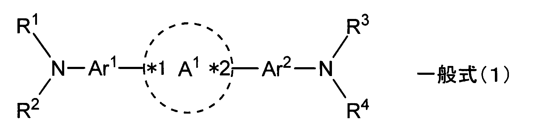
一般式(1)中、R1~R4は、それぞれ独立に、アルキル基、置換基を有してもよいアリール基、置換基を有してもよいヘテロアリール基、または置換基を有してもよいアルケニル基を表す。なかでも、光電変換素子の応答性、および/または、製造適性がより優れる点(以後、単に「本発明の効果がより優れる点」とも称する)で、置換基を有してもよいアリール基、または、置換基を有してもよいヘテロアリール基が好ましく、置換基を有してもよいアリール基がより好ましい。
また、R1、R2、R3、および、R4のうち、後述する環を形成する基に含まれる基は、本発明の効果がより優れる点で、置換基を有してもよいアリール基または置換基を有してもよいヘテロアリール基であることが好ましい。つまり、例えば、R1とAr1とで環を形成する場合、R1が置換基を有してもよいアリール基または置換基を有してもよいヘテロアリール基であることが好ましい。
また、R1、R2、R3、および、R4のうち、後述する環を形成する基に含まれる基は、本発明の効果がより優れる点で、置換基を有してもよいアリール基または置換基を有してもよいヘテロアリール基であることが好ましい。つまり、例えば、R1とAr1とで環を形成する場合、R1が置換基を有してもよいアリール基または置換基を有してもよいヘテロアリール基であることが好ましい。
アルキル基中の炭素数は特に制限されないが、本発明の効果がより優れる点で、1~10が好ましく、1~6がより好ましく、1~3がさらに好ましい。アルキル基としては、直鎖状、分岐状、環状のいずれの構造であってもよい。
アルキル基として好ましいものは、例えば、メチル基、エチル基、n-プロピル基、i-プロピル基、n―ブチル基、n-ヘキシル基などが挙げられる。
アルキル基として好ましいものは、例えば、メチル基、エチル基、n-プロピル基、i-プロピル基、n―ブチル基、n-ヘキシル基などが挙げられる。
アリール基中の炭素数は特に制限されないが、本発明の効果がより優れる点で、6~30が好ましく、6~18がより好ましい。アリール基は、単環構造でも、2環以上の環が縮環した縮合環構造でもよく、後述する置換基Wを有していてもよい。
アリール基としては、例えば、フェニル基、ナフチル基、アントリル基、ピレニル基、フェナントレニル基、メチルフェニル基、ジメチルフェニル基、ビフェニル基、フルオレニル基などが挙げられ、フェニル基、ナフチル基、またはアントリル基が好ましい。
アリール基としては、例えば、フェニル基、ナフチル基、アントリル基、ピレニル基、フェナントレニル基、メチルフェニル基、ジメチルフェニル基、ビフェニル基、フルオレニル基などが挙げられ、フェニル基、ナフチル基、またはアントリル基が好ましい。
ヘテロアリール基(1価の芳香族複素環基)中の炭素数は特に制限されないが、本発明の効果がより優れる点で、3~30が好ましく、3~18がより好ましい。ヘテロアリール基は、後述する置換基Wを有していてもよい。
ヘテロアリール基には炭素原子および水素原子以外にヘテロ原子が含まれ、ヘテロ原子としては、例えば、窒素原子、硫黄原子、酸素原子、セレン原子、テルル原子、リン原子、ケイ素原子、またはホウ素原子が挙げられ、窒素原子、硫黄原子、または酸素原子が好ましい。ヘテロアリール基に含まれるヘテロ原子の数は特に制限されず、通常、1~10個程度であり、1~4個が好ましい。
ヘテロアリール基の環員数は特に制限されないが、好ましくは3~8員環であり、より好ましくは5~7員環であり、特に好ましくは5~6員環である。
ヘテロアリール基としては、例えば、ピリジル基、キノリル基、イソキノリル基、アクリジニル基、フェナントリジニル基、プテリジニル基、ピラジニル基、キノキサリニル基、ピリミジニル基、キナゾリニル基、ピリダジニル基、シンノリニル基、フタラジニル基、トリアジニル基、オキサゾリル基、ベンゾオキサゾリル基、チアゾリル基、ベンゾチアゾリル基、イミダゾリル基、ベンゾイミダゾリル基、ピラゾリル基、インダゾリル基、イソオキサゾリル基、ベンゾイソオキサゾリル基、イソチアゾリル基、ベンゾイソチアゾリル基、オキサジアゾリル基、チアジアゾリル基、トリアゾリル基、テトラゾリル基、フリル基、ベンゾフリル基、チエニル基、ベンゾチエニル基、チエノチエニル基、ジベンゾフリル基、ジベンゾチエニル基、ピロリル基、インドリル基、イミダゾピリジニル基、カルバゾリル基などが挙げられる。
ヘテロアリール基には炭素原子および水素原子以外にヘテロ原子が含まれ、ヘテロ原子としては、例えば、窒素原子、硫黄原子、酸素原子、セレン原子、テルル原子、リン原子、ケイ素原子、またはホウ素原子が挙げられ、窒素原子、硫黄原子、または酸素原子が好ましい。ヘテロアリール基に含まれるヘテロ原子の数は特に制限されず、通常、1~10個程度であり、1~4個が好ましい。
ヘテロアリール基の環員数は特に制限されないが、好ましくは3~8員環であり、より好ましくは5~7員環であり、特に好ましくは5~6員環である。
ヘテロアリール基としては、例えば、ピリジル基、キノリル基、イソキノリル基、アクリジニル基、フェナントリジニル基、プテリジニル基、ピラジニル基、キノキサリニル基、ピリミジニル基、キナゾリニル基、ピリダジニル基、シンノリニル基、フタラジニル基、トリアジニル基、オキサゾリル基、ベンゾオキサゾリル基、チアゾリル基、ベンゾチアゾリル基、イミダゾリル基、ベンゾイミダゾリル基、ピラゾリル基、インダゾリル基、イソオキサゾリル基、ベンゾイソオキサゾリル基、イソチアゾリル基、ベンゾイソチアゾリル基、オキサジアゾリル基、チアジアゾリル基、トリアゾリル基、テトラゾリル基、フリル基、ベンゾフリル基、チエニル基、ベンゾチエニル基、チエノチエニル基、ジベンゾフリル基、ジベンゾチエニル基、ピロリル基、インドリル基、イミダゾピリジニル基、カルバゾリル基などが挙げられる。
アルケニル基中の炭素数は特に制限されないが、本発明の効果がより優れる点で、2~10が好ましく、2~6がより好ましい。アルケニル基としては、直鎖状、分岐状、環状のいずれの構造であってもよく、後述する置換基Wを有していてもよい。
アルケニル基として好ましいものは、例えば、ビニル基、1-プロペニル基などが挙げられる。
アルケニル基として好ましいものは、例えば、ビニル基、1-プロペニル基などが挙げられる。
本明細書における置換基Wについて記載する。
置換基Wとしては、ハロゲン原子、アルキル基(シクロアルキル基、ビシクロアルキル基、トリシクロアルキル基を含む)、アルケニル基(シクロアルケニル基、ビシクロアルケニル基を含む)、アルキニル基、アリール基、複素環基(ヘテロ環基といってもよい)、シアノ基、ヒドロキシ基、ニトロ基、カルボキシ基、アルコキシ基、アリールオキシ基、シリルオキシ基、ヘテロ環オキシ基、アシルオキシ基、カルバモイルオキシ基、アルコキシカルボニルオキシ基、アリールオキシカルボニルオキシ基、アミノ基(アニリノ基を含む)、アンモニオ基、アシルアミノ基、アミノカルボニルアミノ基、アルコキシカルボニルアミノ基、アリールオキシカルボニルアミノ基、スルファモイルアミノ基、アルキルまたはアリールスルホニルアミノ基、メルカプト基、アルキルチオ基、アリールチオ基、ヘテロ環チオ基、スルファモイル基、スルホ基、アルキルまたはアリールスルフィニル基、アルキルまたはアリールスルホニル基、アシル基、アリールオキシカルボニル基、アルコキシカルボニル基、カルバモイル基、アリールまたはヘテロ環アゾ基、イミド基、ホスフィノ基、ホスフィニル基、ホスフィニルオキシ基、ホスフィニルアミノ基、ホスホノ基、シリル基、ヒドラジノ基、ウレイド基、ボロン酸基(-B(OH)2)、ホスファト基(-OPO(OH)2)、スルファト基(-OSO3H)、その他の公知の置換基が挙げられる。
なお、置換基Wの詳細については、特開2007-234651号公報の段落[0023]に記載される。
置換基Wとしては、ハロゲン原子、アルキル基(シクロアルキル基、ビシクロアルキル基、トリシクロアルキル基を含む)、アルケニル基(シクロアルケニル基、ビシクロアルケニル基を含む)、アルキニル基、アリール基、複素環基(ヘテロ環基といってもよい)、シアノ基、ヒドロキシ基、ニトロ基、カルボキシ基、アルコキシ基、アリールオキシ基、シリルオキシ基、ヘテロ環オキシ基、アシルオキシ基、カルバモイルオキシ基、アルコキシカルボニルオキシ基、アリールオキシカルボニルオキシ基、アミノ基(アニリノ基を含む)、アンモニオ基、アシルアミノ基、アミノカルボニルアミノ基、アルコキシカルボニルアミノ基、アリールオキシカルボニルアミノ基、スルファモイルアミノ基、アルキルまたはアリールスルホニルアミノ基、メルカプト基、アルキルチオ基、アリールチオ基、ヘテロ環チオ基、スルファモイル基、スルホ基、アルキルまたはアリールスルフィニル基、アルキルまたはアリールスルホニル基、アシル基、アリールオキシカルボニル基、アルコキシカルボニル基、カルバモイル基、アリールまたはヘテロ環アゾ基、イミド基、ホスフィノ基、ホスフィニル基、ホスフィニルオキシ基、ホスフィニルアミノ基、ホスホノ基、シリル基、ヒドラジノ基、ウレイド基、ボロン酸基(-B(OH)2)、ホスファト基(-OPO(OH)2)、スルファト基(-OSO3H)、その他の公知の置換基が挙げられる。
なお、置換基Wの詳細については、特開2007-234651号公報の段落[0023]に記載される。
Ar1およびAr2は、それぞれ独立に、置換基を有してもよいアリーレン基または置換基を有してもよいヘテロアリーレン基を表す。
アリーレン基中の炭素数は特に制限されないが、本発明の効果がより優れる点で、6~30が好ましく、6~20がより好ましい。
アリーレン基としては、例えば、フェニレン基、ビフェニレン基、ターフェニレン基、ナフチレン基、アントリレン基、フェナントリレン基、ピレンジイル基、ペリレンジイル基、フルオレンジイル基、クリセンジイル基、トリフェニレンジイル基、ベンゾアントラセンジイル基、ベンゾフェナントレンジイル基などが挙げられる。
ヘテロアリーレン基中の炭素数は特に制限されないが、本発明の効果がより優れる点で、1~20が好ましく、2~12がより好ましい。
ヘテロアリーレン基としては、例えば、ピリジレン基、キノリレン基、イソキノリレン基、アクリジンジイル基、フェナントリジンジイル基、ピラジンジイル基、キノキサリンジイル基、ピリミジンジイル基、トリアジンジイル基、イミダゾールジイル基、ピラゾールジイル基、オキサジアゾールジイル基、トリアゾールジイル基、フリレン基、チエニレン基、ピロールジイル基、インドールジイル基、カルバゾールジイル基などが挙げられる。
上記アリーレン基および上記ヘテロアリーレン基は、置換基を有していてもよく、置換基としては上記置換基Wが挙げられる。
アリーレン基中の炭素数は特に制限されないが、本発明の効果がより優れる点で、6~30が好ましく、6~20がより好ましい。
アリーレン基としては、例えば、フェニレン基、ビフェニレン基、ターフェニレン基、ナフチレン基、アントリレン基、フェナントリレン基、ピレンジイル基、ペリレンジイル基、フルオレンジイル基、クリセンジイル基、トリフェニレンジイル基、ベンゾアントラセンジイル基、ベンゾフェナントレンジイル基などが挙げられる。
ヘテロアリーレン基中の炭素数は特に制限されないが、本発明の効果がより優れる点で、1~20が好ましく、2~12がより好ましい。
ヘテロアリーレン基としては、例えば、ピリジレン基、キノリレン基、イソキノリレン基、アクリジンジイル基、フェナントリジンジイル基、ピラジンジイル基、キノキサリンジイル基、ピリミジンジイル基、トリアジンジイル基、イミダゾールジイル基、ピラゾールジイル基、オキサジアゾールジイル基、トリアゾールジイル基、フリレン基、チエニレン基、ピロールジイル基、インドールジイル基、カルバゾールジイル基などが挙げられる。
上記アリーレン基および上記ヘテロアリーレン基は、置換基を有していてもよく、置換基としては上記置換基Wが挙げられる。
また、Ar1とR1、Ar1とR2、R1とR2、Ar2とR3、Ar2とR4およびR3とR4のうち、少なくとも一つはそれぞれ互いに結合して環を形成する。なお、結合に際しては、Ar1とR1、Ar1とR2、R1とR2、Ar2とR3、Ar2とR4、R3とR4は、それぞれ互いに直接または連結基を介して結合して環を形成することが好ましく、本発明の効果がより優れる点で、直接結合して環を形成する、または、アルキレン基を介して環を形成することがより好ましい。
なお、連結基の構造は特に制限されないが、例えば、酸素原子、硫黄原子、アルキレン基、シリレン基、アルケニレン基、シクロアルキレン基、シクロアルケニレン基、アリーレン基、2価の複素環基、イミノ基、またはこれらを組み合わせた基が挙げられ、これらは更に置換基を有してもよい。好ましくはアルキレン基、シリレン基、アルケニレン基、シクロアルキレン基、シクロアルケニレン基、アリーレン基等であり、アルキレン基がより好ましい。
形成される環の構造は特に制限されず、例えば、ヘテロ原子を有してもよい脂肪族環や、ヘテロ原子を有してもよい芳香族環などが挙げられ、本発明の効果がより優れる点で、ヘテロ原子を有してもよい芳香族環が挙げられる。
なお、連結基の構造は特に制限されないが、例えば、酸素原子、硫黄原子、アルキレン基、シリレン基、アルケニレン基、シクロアルキレン基、シクロアルケニレン基、アリーレン基、2価の複素環基、イミノ基、またはこれらを組み合わせた基が挙げられ、これらは更に置換基を有してもよい。好ましくはアルキレン基、シリレン基、アルケニレン基、シクロアルキレン基、シクロアルケニレン基、アリーレン基等であり、アルキレン基がより好ましい。
形成される環の構造は特に制限されず、例えば、ヘテロ原子を有してもよい脂肪族環や、ヘテロ原子を有してもよい芳香族環などが挙げられ、本発明の効果がより優れる点で、ヘテロ原子を有してもよい芳香族環が挙げられる。
なお、本発明の効果がより優れる点で、Ar1とR1、Ar1とR2、およびR1とR2の中でも少なくとも1つがそれぞれ互いに結合して環を形成すると共に、Ar2とR3、Ar2とR4およびR3とR4の中でも少なくとも1つがそれぞれ互いに結合して環を形成することが好ましく、Ar1とR1、および、Ar2とR3が、それぞれ互いに結合して環を形成することがより好ましい。
A1は、一般式(2-1)で表される基~一般式(2-3)で表される基からなる群から選択されるいずれか一つの基を表す。なかでも、本発明の効果がより優れる点で、一般式(2-1)で表される基が好ましい。
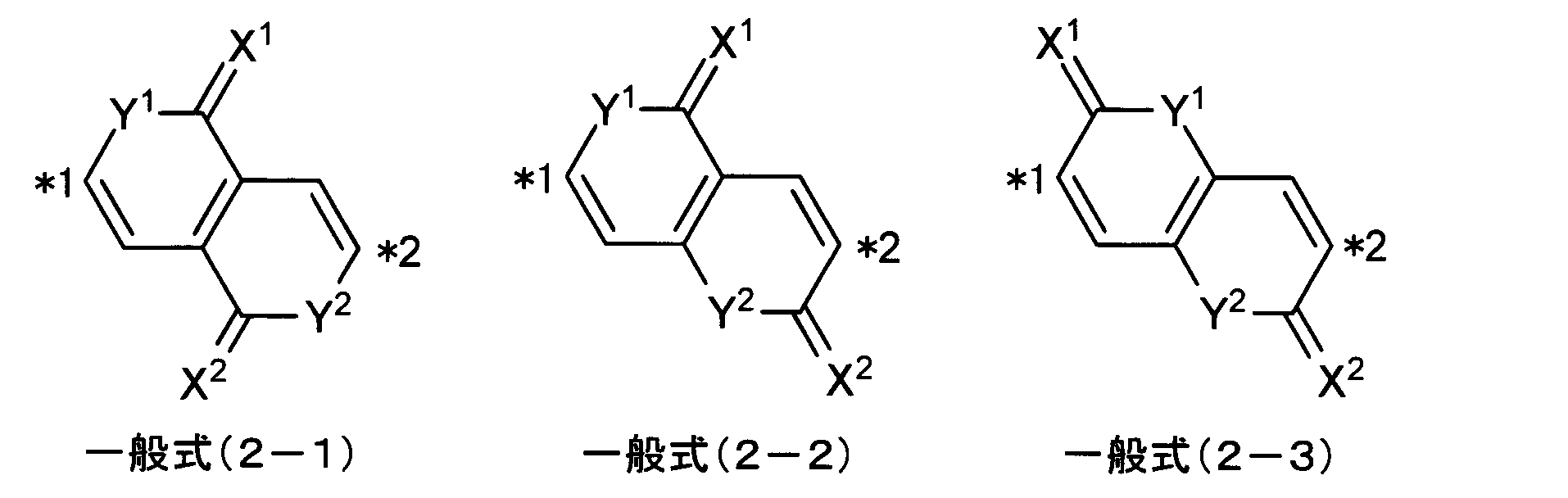
一般式(2-1)~(2-3)中、X1およびX2は、それぞれ独立に、酸素原子、硫黄原子、セレン原子、=NRa1、または、=CRa2Ra3を表す。なかでも、本発明の効果がより優れる点で、酸素原子または硫黄原子が好ましく、酸素原子がより好ましい。
Ra1は、水素原子または置換基を表す。置換基としては、上記置換基Wが挙げられ、なかでも、本発明の効果がより優れる点で、アルキル基またはアリール基が好ましい。
Ra2およびRa3は、それぞれ独立にシアノ基、カルボニル基またはアルコキシカルボニル基を表す。
Ra1は、水素原子または置換基を表す。置換基としては、上記置換基Wが挙げられ、なかでも、本発明の効果がより優れる点で、アルキル基またはアリール基が好ましい。
Ra2およびRa3は、それぞれ独立にシアノ基、カルボニル基またはアルコキシカルボニル基を表す。
Y1およびY2は、それぞれ独立に、酸素原子、硫黄原子、セレン原子、>NRb1、>CRb2Rb3、または、>SiRb4Rb5を表す。なかでも、本発明の効果がより優れる点で、酸素原子または硫黄原子が好ましく、酸素原子がより好ましい。
Rb1~Rb5は、それぞれ独立に、水素原子または置換基を表す。置換基としては、上記置換基Wが挙げられ、なかでも、本発明の効果がより優れる点で、アルキル基が好ましい。
Rb1~Rb5は、それぞれ独立に、水素原子または置換基を表す。置換基としては、上記置換基Wが挙げられ、なかでも、本発明の効果がより優れる点で、アルキル基が好ましい。
なお、一般式(1)中の*1、*2は、それぞれ一般式(2-1)~(2-3)の*1、*2に結合していることを表す。より具体的には、以下に一般式(2-1)~(2-3)で表される基が、一般式(1)中のA1に導入された場合の構造式の例を示す。

なお、一般式(1)で表される化合物の好適態様の一つとしては、以下の一般式(X)で表される化合物が挙げられる。

一般式(X)中、R11~R14、R21~R25、R31~R35、R41~R44、R51~R55、および、R61~R65は、それぞれ独立に、水素原子、または、置換基を表す。置換基としては、例えば、上述した置換基Wが挙げられる。
なお、R12とR21、R25とR31、R13とR35、R42とR51、R55とR61、および、R43とR65のうち、少なくとも一つはそれぞれ互いに結合して環を形成する。なかでも、本発明の効果がより優れる点で、R12とR21、R25とR31、および、R13とR35のうち少なくとも一つと、R42とR51、R55とR61、および、R43とR65のうち少なくとも一つとが、それぞれ互いに結合して環を形成することが好ましく、R12とR21およびR42とR51がそれぞれ互いに結合して環を形成することがより好ましい。
なお、結合に際しては、上述したように、それぞれ互いに直接または連結基を介して結合して環を形成してもよく、連結基の種類は上述の通りである。
また、A1の定義は、上述の通りである。
なお、R12とR21、R25とR31、R13とR35、R42とR51、R55とR61、および、R43とR65のうち、少なくとも一つはそれぞれ互いに結合して環を形成する。なかでも、本発明の効果がより優れる点で、R12とR21、R25とR31、および、R13とR35のうち少なくとも一つと、R42とR51、R55とR61、および、R43とR65のうち少なくとも一つとが、それぞれ互いに結合して環を形成することが好ましく、R12とR21およびR42とR51がそれぞれ互いに結合して環を形成することがより好ましい。
なお、結合に際しては、上述したように、それぞれ互いに直接または連結基を介して結合して環を形成してもよく、連結基の種類は上述の通りである。
また、A1の定義は、上述の通りである。
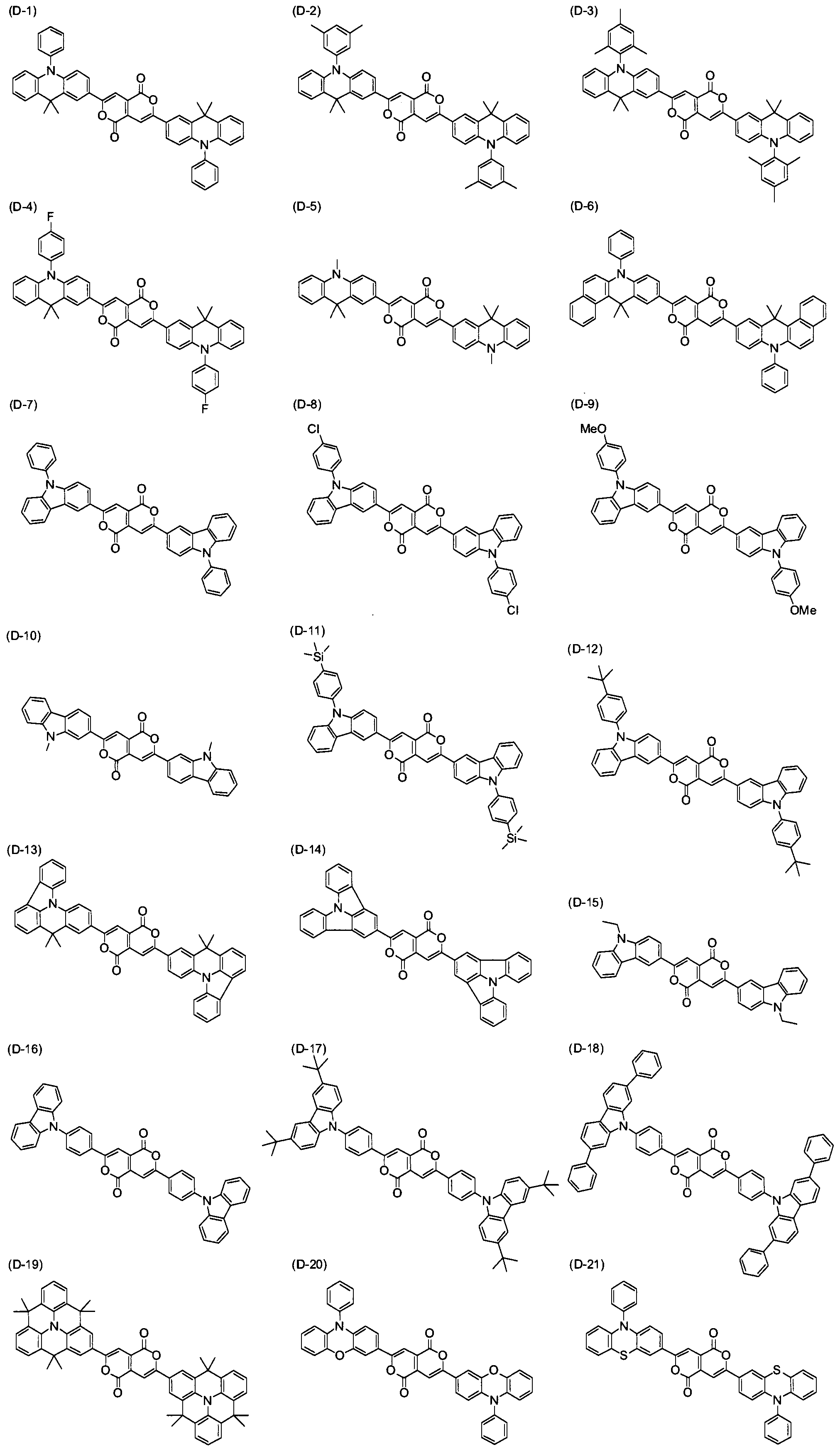
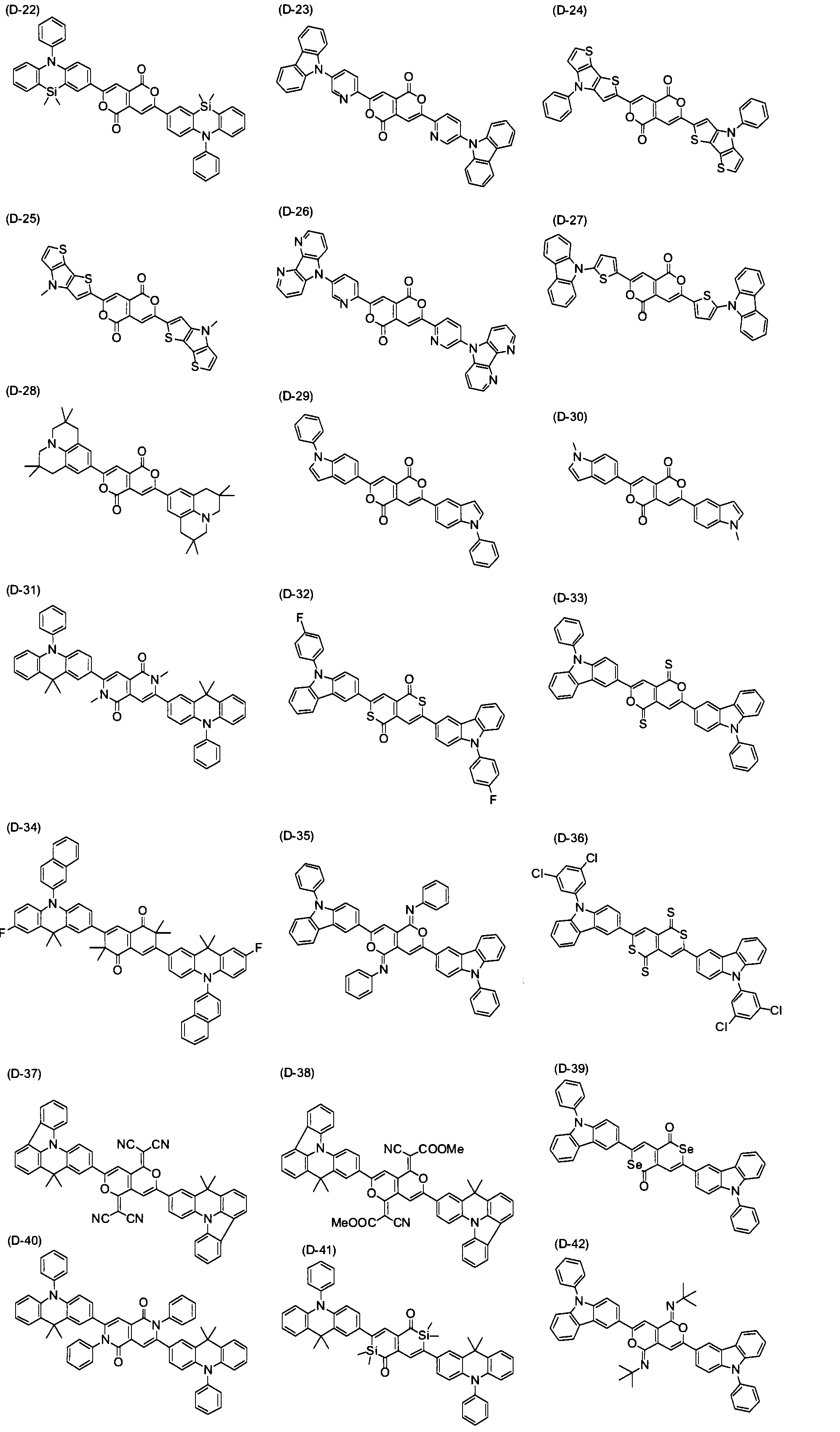
以下に、一般式(1)で表される化合物を例示する。ここで、下記具体例中のMeはメチルを表す。


一般式(1)で表される化合物の双極子モーメントは特に制限されないが、本発明の効果がより優れる点で、1D以下が好ましく、0.5D以下がより好ましい。
上記双極子モーメントは計算で求めることができ、具体的には分子軌道計算ソフトGaussian09(ガウシアン社製)により、B3LYP法に基底関数6-31G(d)を用いて求めることができる。
上記双極子モーメントは計算で求めることができ、具体的には分子軌道計算ソフトGaussian09(ガウシアン社製)により、B3LYP法に基底関数6-31G(d)を用いて求めることができる。
一般式(1)で表される化合物は紫外可視吸収スペクトルにおいて、400nm以上720nm未満に吸収極大を有することが好ましい。吸収スペクトルのピーク波長(吸収極大波長)は、可視領域の光、特にG領域(500-600nm)の光を中心に吸収するという観点から450nm以上700nm以下であることがより好ましく、480nm以上650nm以下がさらに好ましく、500nm以上600nm以下であることが特に好ましい。
一般式(1)で表される化合物の吸収極大波長は、化合物のクロロホルム溶液を、島津製作所社製UV-2550を用いて測定することができる。クロロホルム溶液の濃度は5×10⁻⁵~1×10⁻⁷mol/lが好ましく、3×10-5~2×10-6mol/lがより好ましく、2×10-5~5×10-6mol/lが特に好ましい。
一般式(1)で表される化合物の吸収極大波長は、化合物のクロロホルム溶液を、島津製作所社製UV-2550を用いて測定することができる。クロロホルム溶液の濃度は5×10⁻⁵~1×10⁻⁷mol/lが好ましく、3×10-5~2×10-6mol/lがより好ましく、2×10-5~5×10-6mol/lが特に好ましい。
一般式(1)で表される化合物は、紫外可視吸収スペクトルにおいて400nm以上720nm未満に吸収極大を有し、その吸収極大波長のモル吸光係数が10000mol-1・l・cm-1以上であることが好ましい。光電変換膜の膜厚を薄くし、高い電荷捕集効率、高速応答性、高感度特性の素子とするには、モル吸光係数が大きい材料が好ましい。一般式(1)で表される化合物のモル吸光係数としては30000mol-1・l・cm-1以上がより好ましく、50000mol-1・l・cm-1以上がさらに好ましい。一般式(1)で表される化合物のモル吸光係数はクロロホルム溶液で測定したものである。
一般式(1)で表される化合物は、融点と蒸着温度の差(融点-蒸着温度)が大きいほど蒸着時に分解しにくく、高い温度をかけて蒸着速度を大きくすることができる。また、融点と蒸着温度の差(融点-蒸着温度)は30℃以上が好ましく、45℃以上がより好ましく、60℃以上が更に好ましい。
一般式(1)で表される化合物の分子量は、300~1500が好ましく、500~1000がより好ましく、本発明の効果がより優れる点で、500以上850未満が特に好ましい。化合物の分子量が1500以下であれば、蒸着温度が高くならず、化合物の分解が起こりにくい。化合物の分子量が300以上であれば蒸着膜のガラス転移点が低くならず、素子の耐熱性が低下しにくい。
一般式(1)で表される化合物のガラス転移点(Tg)は、95℃以上が好ましく、110℃以上がより好ましく、135℃以上がさらに好ましく、150℃以上が特に好ましく、160℃以上が最も好ましい。ガラス転移点が高くなると、素子の耐熱性が向上するため好ましい。
一般式(1)で表される化合物は、撮像素子、光センサ、または光電池に用いる光電変換膜の材料として特に有用である。なお、通常、一般式(1)で表される化合物は、光電変換膜内で有機p型化合物として機能する。また、他の用途として、着色材料、液晶材料、有機半導体材料、有機発光素子材料、電荷輸送材料、医薬材料、蛍光診断薬材料、等としても用いることもできる。
(その他材料)
光電変換膜は、さらに有機p型化合物または有機n型化合物の光電変換材料を含有してもよい。
有機p型化合物(有機p型半導体)は、ドナー性有機半導体(化合物)であり、主に正孔輸送性有機化合物に代表され、電子を供与しやすい性質がある有機化合物をいう。さらに詳しくは、2つの有機材料を接触させて用いたときにイオン化ポテンシャルの小さい方の有機化合物をいう。したがって、ドナー性有機化合物は、電子供与性のある有機化合物であればいずれの有機化合物も使用可能である。例えば、トリアリールアミン化合物、ベンジジン化合物、ピラゾリン化合物、スチリルアミン化合物、ヒドラゾン化合物、トリフェニルメタン化合物、カルバゾール化合物等を用いることができる。
光電変換膜は、さらに有機p型化合物または有機n型化合物の光電変換材料を含有してもよい。
有機p型化合物(有機p型半導体)は、ドナー性有機半導体(化合物)であり、主に正孔輸送性有機化合物に代表され、電子を供与しやすい性質がある有機化合物をいう。さらに詳しくは、2つの有機材料を接触させて用いたときにイオン化ポテンシャルの小さい方の有機化合物をいう。したがって、ドナー性有機化合物は、電子供与性のある有機化合物であればいずれの有機化合物も使用可能である。例えば、トリアリールアミン化合物、ベンジジン化合物、ピラゾリン化合物、スチリルアミン化合物、ヒドラゾン化合物、トリフェニルメタン化合物、カルバゾール化合物等を用いることができる。
有機n型化合物(有機n型半導体)とは、アクセプター性有機半導体であり、主に電子輸送性有機化合物に代表され、電子を受容しやすい性質がある有機化合物をいう。更に詳しくは、2つの有機化合物を接触させて用いたときに電子親和力の大きい方の有機化合物をいう。したがって、アクセプター性有機半導体は、電子受容性のある有機化合物であればいずれの有機化合物も使用可能である。好ましくは、フラーレンまたはフラーレン誘導体、縮合芳香族炭素環化合物(ナフタレン誘導体、アントラセン誘導体、フェナントレン誘導体、テトラセン誘導体、ピレン誘導体、ペリレン誘導体、フルオランテン誘導体)、窒素原子、酸素原子、硫黄原子を含有する5~7員のヘテロ環化合物(例えば、ピリジン、ピラジン、ピリミジン、ピリダジン、トリアジン、キノリン、キノキサリン、キナゾリン、フタラジン、シンノリン、イソキノリン、プテリジン、アクリジン、フェナジン、フェナントロリン、テトラゾール、ピラゾール、イミダゾール、チアゾール、オキサゾール、インダゾール、ベンゾイミダゾール、ベンゾトリアゾール、ベンゾオキサゾール、ベンゾチアゾール、カルバゾール、プリン、トリアゾロピリダジン、トリアゾロピリミジン、テトラザインデン、オキサジアゾール、イミダゾピリジン、ピラジン、ピロロピリジン、チアジアゾロピリジン、ジベンゾアゼピン、トリベンゾアゼピン等)、ポリアリーレン化合物、フルオレン化合物、シクロペンタジエン化合物、シリル化合物、含窒素ヘテロ環化合物を配位子として有する金属錯体などが挙げられる。
上記有機n型化合物として、後述する図3に示したような態様で用いる場合には、フラーレンおよびフラーレン誘導体からなる群から選択されるフラーレン類が好ましい。フラーレンとは、フラーレンC60、フラーレンC70、フラーレンC76、フラーレンC78、フラーレンC80、フラーレンC82、フラーレンC84、フラーレンC90、フラーレンC96、フラーレンC240、フラーレンC540、ミックスドフラーレンを表し、フラーレン誘導体とはこれらに置換基が付加された化合物のことを表す。置換基としては、アルキル基、アリール基、または複素環基が好ましい。フラーレン誘導体としては、特開2007-123707号公報に記載の化合物が好ましい。
一方で図2に示したような態様で用いる場合には有機n型化合物は無色、または、有機p型化合物に近い吸収極大波長および/または吸収波形を持つことが望ましく、具体的な数値としては吸収極大波長が400nm以下、または、500nm以上600nm以下であることが望ましい。前述の有機n型化合物の特徴を持ち、吸収が適した化合物であればどのような化合物でも用いることができ、例えば、US2013-0112947号の[0016]~[0019]に記載の化合物などがある。
光電変換膜は、上記一般式(1)で表される化合物と、有機n型化合物とが混合された状態で形成されるバルクヘテロ構造をなしていることが好ましい。バルクヘテロ構造は光電変換膜内で、有機p型化合物と有機n型化合物が混合、分散している層であり、湿式法、乾式法のいずれでも形成できるが、共蒸着法で形成するものが好ましい。へテロ接合構造を含有させることにより、光電変換膜のキャリア拡散長が短いという欠点を補い、光電変換膜の光電変換効率を向上させることができる。なお、バルクへテロ接合構造については、特開2005-303266号公報の[0013]~[0014]等において詳細に説明されている。
光電変換素子の応答性の観点から、一般式(1)で表される化合物と有機n型化合物との合計の含有量に対する有機n型化合物の含有量(=有機n型化合物の単層換算での膜厚/一般式(1)で表される化合物の単層換算での膜厚+有機n型化合物の単層換算での膜厚))は、有機n型化合物がフラーレン類である場合、50体積%以上であることが好ましく、55体積%以上であることがより好ましく、65体積%以上であることがさらに好ましい。上限は特に制限されないが、95体積%以下であることが好ましく、90体積%以下であることがより好ましい。有機n型化合物がフラーレン類以外の化合物である場合には、上記含有量は、20体積%以上80体積%以下であることが好ましく、30体積%以上70体積%以下であることがより好ましく、40体積%以上60体積%以下であることがさらに好ましい。
本発明の一般式(1)で表される化合物および有機n型化合物が含まれる光電変換膜は非発光性膜であり、有機電界発光素子(OLED)とは異なる特徴を有する。非発光性膜とは発光量子効率が1%以下の膜の場合であり、0.5%以下であることがより好ましく、0.1%以下であることが更に好ましい。
(成膜方法)
光電変換膜は、主に、乾式成膜法により成膜することができる。乾式成膜法の具体例としては、蒸着法(特に、真空蒸着法)、スパッタリング法、イオンプレーティング法,MBE法等の物理気相成長法、または、プラズマ重合等のCVD法が挙げられる。好ましくは、真空蒸着法が好ましい。真空蒸着法により成膜する場合、真空度、蒸着温度等の製造条件は常法に従って設定することができる。
光電変換膜は、主に、乾式成膜法により成膜することができる。乾式成膜法の具体例としては、蒸着法(特に、真空蒸着法)、スパッタリング法、イオンプレーティング法,MBE法等の物理気相成長法、または、プラズマ重合等のCVD法が挙げられる。好ましくは、真空蒸着法が好ましい。真空蒸着法により成膜する場合、真空度、蒸着温度等の製造条件は常法に従って設定することができる。
光電変換膜の厚みは、10nm以上1000nm以下が好ましく、50nm以上800nm以下がより好ましく、100nm以上500nm以下が特に好ましい。10nm以上とすることにより、好適な暗電流抑制効果が得られ、1000nm以下とすることにより、好適な光電変換効率が得られる。
[電極]
電極(上部電極(透明導電性膜)15と下部電極(導電性膜)11)は、導電性材料から構成される。導電性材料としては、金属、合金、金属酸化物、電気伝導性化合物、またはこれらの混合物などを用いることができる。
上部電極15から光が入射されるため、上部電極15は検知したい光に対し十分透明であることが好ましい。具体的には、アンチモンやフッ素等をドープした酸化錫(ATO、FTO)、酸化錫、酸化亜鉛、酸化インジウム、酸化インジウム錫(ITO)、酸化亜鉛インジウム(IZO)等の導電性金属酸化物、金、銀、クロム、ニッケル等の金属薄膜、更にこれらの金属と導電性金属酸化物との混合物または積層物、ヨウ化銅、硫化銅などの無機導電性物質、ポリアニリン、ポリチオフェン、ポリピロールなどの有機導電性材料、およびこれらとITOとの積層物などが挙げられる。この中で好ましいのは、高導電性、透明性等の点から、透明導電性金属酸化物である。
電極(上部電極(透明導電性膜)15と下部電極(導電性膜)11)は、導電性材料から構成される。導電性材料としては、金属、合金、金属酸化物、電気伝導性化合物、またはこれらの混合物などを用いることができる。
上部電極15から光が入射されるため、上部電極15は検知したい光に対し十分透明であることが好ましい。具体的には、アンチモンやフッ素等をドープした酸化錫(ATO、FTO)、酸化錫、酸化亜鉛、酸化インジウム、酸化インジウム錫(ITO)、酸化亜鉛インジウム(IZO)等の導電性金属酸化物、金、銀、クロム、ニッケル等の金属薄膜、更にこれらの金属と導電性金属酸化物との混合物または積層物、ヨウ化銅、硫化銅などの無機導電性物質、ポリアニリン、ポリチオフェン、ポリピロールなどの有機導電性材料、およびこれらとITOとの積層物などが挙げられる。この中で好ましいのは、高導電性、透明性等の点から、透明導電性金属酸化物である。
通常、導電性膜をある範囲より薄くすると、急激な抵抗値の増加をもたらすが、本実施形態に係る光電変換素子を組み込んだ固体撮像素子では、シート抵抗は、好ましくは100~10000Ω/□でよく、薄膜化できる膜厚の範囲の自由度は大きい。また、上部電極(透明導電性膜)15は厚みが薄いほど吸収する光の量は少なくなり、一般に光透過率が増す。光透過率の増加は、光電変換膜での光吸収を増大させ、光電変換能を増大させるため、非常に好ましい。薄膜化に伴う、リーク電流の抑制、薄膜の抵抗値の増大、透過率の増加を考慮すると、上部電極15の膜厚は、5~100nmであることが好ましく、更に好ましくは5~20nmであることが望ましい。
下部電極11は、用途に応じて、透明性を持たせる場合と、逆に透明を持たせず光を反射させるような材料を用いる場合等がある。具体的には、アンチモンやフッ素等をドープした酸化錫(ATO、FTO)、酸化錫、酸化亜鉛、酸化インジウム、酸化インジウム錫(ITO)、酸化亜鉛インジウム(IZO)等の導電性金属酸化物、金、銀、クロム、ニッケル、チタン、タングステン、アルミ等の金属およびこれらの金属の酸化物や窒化物などの導電性化合物(一例として窒化チタン(TiN)を挙げる)、更にこれらの金属と導電性金属酸化物との混合物または積層物、ヨウ化銅、硫化銅などの無機導電性物質、ポリアニリン、ポリチオフェン、ポリピロールなどの有機導電性材料、およびこれらとITOまたは窒化チタンとの積層物などが挙げられる。
電極を形成する方法は特に限定されず、電極材料に応じて適宜選択することができる。具体的には、印刷方式、コーティング方式等の湿式方式、真空蒸着法、スパッタリング法、イオンプレーティング法等の物理的方式、CVD、プラズマCVD法等の化学的方式等により形成することができる。
電極の材料がITOの場合、電子ビーム法、スパッタリング法、抵抗加熱蒸着法、化学反応法(ゾル-ゲル法など)、酸化インジウムスズの分散物の塗布などの方法で形成することができる。更に、ITOを用いて作製された膜に、UV-オゾン処理、プラズマ処理などを施すことができる。電極の材料がTiNの場合、反応性スパッタリング法をはじめとする各種の方法が用いられ、更にUV-オゾン処理、プラズマ処理などを施すことができる。
電極の材料がITOの場合、電子ビーム法、スパッタリング法、抵抗加熱蒸着法、化学反応法(ゾル-ゲル法など)、酸化インジウムスズの分散物の塗布などの方法で形成することができる。更に、ITOを用いて作製された膜に、UV-オゾン処理、プラズマ処理などを施すことができる。電極の材料がTiNの場合、反応性スパッタリング法をはじめとする各種の方法が用いられ、更にUV-オゾン処理、プラズマ処理などを施すことができる。
[電荷ブロッキング膜:電子ブロッキング膜、正孔ブロッキング膜]
本発明の光電変換素子は、電荷ブロッキング膜を有していてもよい。この膜を有することにより、得られる光電変換素子の特性(光電変換効率、応答速度など)がより優れる。電荷ブロッキング膜としては、電子ブロッキング膜と正孔ブロッキング膜とが挙げられる。以下に、それぞれの膜について詳述する。
本発明の光電変換素子は、電荷ブロッキング膜を有していてもよい。この膜を有することにより、得られる光電変換素子の特性(光電変換効率、応答速度など)がより優れる。電荷ブロッキング膜としては、電子ブロッキング膜と正孔ブロッキング膜とが挙げられる。以下に、それぞれの膜について詳述する。
(電子ブロッキング膜)
電子ブロッキング膜には、電子供与性有機材料を用いることができる。具体的には、低分子材料では、N,N’-ビス(3-メチルフェニル)-(1,1’-ビフェニル)-4,4’-ジアミン(TPD)や4,4’-ビス[N-(ナフチル)-N-フェニル-アミノ]ビフェニル(α-NPD)等の芳香族ジアミン化合物、オキサゾール、オキサジアゾール、トリアゾール、イミダゾール、イミダゾロン、スチルベン誘導体、テトラヒドロイミダゾール、ポリアリールアルカン、ブタジエン、4,4’,4”トリス(N-(3-メチルフェニル)N-フェニルアミノ)トリフェニルアミン(m-MTDATA)、ポルフィリン、テトラフェニルポルフィリン銅、フタロシアニン、銅フタロシアニン、チタニウムフタロシアニンオキサイド等のポルフィリン化合物、トリアゾール誘導体、オキサジアゾール誘導体、イミダゾール誘導体、ポリアリールアルカン誘導体、ピラゾリン誘導体、ピラゾロン誘導体、フェニレンジアミン誘導体、アリールアミン誘導体、アミノ置換カルコン誘導体、オキサゾール誘導体、スチリルアントラセン誘導体、フルオレノン誘導体、ヒドラゾン誘導体、シラザン誘導体などを用いることができ、高分子材料では、フェニレンビニレン、フルオレン、カルバゾール、インドール、ピレン、ピロール、ピコリン、チオフェン、アセチレン、ジアセチレン等の重合体や、その誘導体を用いることができる。電子供与性化合物でなくとも、十分なホール輸送性を有する化合物であれば用いることは可能である。具体的には特開2008-72090号公報の[0083]~[0089]、特開2011-176259号公報の[0043]~[0063]、特開2011-228614号公報の[0121]~[0148]、特開2011-228615号公報の[0108]~[0156]に記載の化合物が好ましい。
電子ブロッキング膜には、電子供与性有機材料を用いることができる。具体的には、低分子材料では、N,N’-ビス(3-メチルフェニル)-(1,1’-ビフェニル)-4,4’-ジアミン(TPD)や4,4’-ビス[N-(ナフチル)-N-フェニル-アミノ]ビフェニル(α-NPD)等の芳香族ジアミン化合物、オキサゾール、オキサジアゾール、トリアゾール、イミダゾール、イミダゾロン、スチルベン誘導体、テトラヒドロイミダゾール、ポリアリールアルカン、ブタジエン、4,4’,4”トリス(N-(3-メチルフェニル)N-フェニルアミノ)トリフェニルアミン(m-MTDATA)、ポルフィリン、テトラフェニルポルフィリン銅、フタロシアニン、銅フタロシアニン、チタニウムフタロシアニンオキサイド等のポルフィリン化合物、トリアゾール誘導体、オキサジアゾール誘導体、イミダゾール誘導体、ポリアリールアルカン誘導体、ピラゾリン誘導体、ピラゾロン誘導体、フェニレンジアミン誘導体、アリールアミン誘導体、アミノ置換カルコン誘導体、オキサゾール誘導体、スチリルアントラセン誘導体、フルオレノン誘導体、ヒドラゾン誘導体、シラザン誘導体などを用いることができ、高分子材料では、フェニレンビニレン、フルオレン、カルバゾール、インドール、ピレン、ピロール、ピコリン、チオフェン、アセチレン、ジアセチレン等の重合体や、その誘導体を用いることができる。電子供与性化合物でなくとも、十分なホール輸送性を有する化合物であれば用いることは可能である。具体的には特開2008-72090号公報の[0083]~[0089]、特開2011-176259号公報の[0043]~[0063]、特開2011-228614号公報の[0121]~[0148]、特開2011-228615号公報の[0108]~[0156]に記載の化合物が好ましい。
なお、電子ブロッキング膜は、複数膜で構成してもよい。
電子ブロッキング膜としては無機材料を用いることもできる。一般的に、無機材料は有機材料よりも誘電率が大きいため、電子ブロッキング膜に用いた場合に、光電変換膜に電圧が多くかかるようになり、光電変換効率を高くすることができる。電子ブロッキング膜となりうる材料としては、酸化カルシウム、酸化クロム、酸化クロム銅、酸化マンガン、酸化コバルト、酸化ニッケル、酸化銅、酸化ガリウム銅、酸化ストロンチウム銅、酸化ニオブ、酸化モリブデン、酸化インジウム銅、酸化インジウム銀、酸化イリジウム等がある。電子ブロッキング膜が単層の場合にはその層を無機材料からなる層とすることができ、または、複数層の場合には1つまたは2以上の層を無機材料からなる層とすることができる。
電子ブロッキング膜としては無機材料を用いることもできる。一般的に、無機材料は有機材料よりも誘電率が大きいため、電子ブロッキング膜に用いた場合に、光電変換膜に電圧が多くかかるようになり、光電変換効率を高くすることができる。電子ブロッキング膜となりうる材料としては、酸化カルシウム、酸化クロム、酸化クロム銅、酸化マンガン、酸化コバルト、酸化ニッケル、酸化銅、酸化ガリウム銅、酸化ストロンチウム銅、酸化ニオブ、酸化モリブデン、酸化インジウム銅、酸化インジウム銀、酸化イリジウム等がある。電子ブロッキング膜が単層の場合にはその層を無機材料からなる層とすることができ、または、複数層の場合には1つまたは2以上の層を無機材料からなる層とすることができる。
(正孔ブロッキング膜)
正孔ブロッキング膜には、電子受容性有機材料を用いることができる。
電子受容性材料としては、1,3-ビス(4-tert-ブチルフェニル-1,3,4-オキサジアゾリル)フェニレン(OXD-7)等のオキサジアゾール誘導体、アントラキノジメタン誘導体、ジフェニルキノン誘導体、バソクプロイン、バソフェナントロリン、およびこれらの誘導体、トリアゾール化合物、トリス(8-ヒドロキシキノリナート)アルミニウム錯体、ビス(4-メチル-8-キノリナート)アルミニウム錯体、ジスチリルアリーレン誘導体、シロール化合物などを用いることができる。また、電子受容性有機材料でなくとも、十分な電子輸送性を有する材料ならば使用することは可能である。ポルフィリン系化合物や、DCM(4-ジシアノメチレン-2-メチル-6-(4-(ジメチルアミノスチリル))-4Hピラン)等のスチリル系化合物、4Hピラン系化合物を用いることができる。具体的には特開2008-72090号公報の[0073]~[0078]に記載の化合物が好ましい。
正孔ブロッキング膜には、電子受容性有機材料を用いることができる。
電子受容性材料としては、1,3-ビス(4-tert-ブチルフェニル-1,3,4-オキサジアゾリル)フェニレン(OXD-7)等のオキサジアゾール誘導体、アントラキノジメタン誘導体、ジフェニルキノン誘導体、バソクプロイン、バソフェナントロリン、およびこれらの誘導体、トリアゾール化合物、トリス(8-ヒドロキシキノリナート)アルミニウム錯体、ビス(4-メチル-8-キノリナート)アルミニウム錯体、ジスチリルアリーレン誘導体、シロール化合物などを用いることができる。また、電子受容性有機材料でなくとも、十分な電子輸送性を有する材料ならば使用することは可能である。ポルフィリン系化合物や、DCM(4-ジシアノメチレン-2-メチル-6-(4-(ジメチルアミノスチリル))-4Hピラン)等のスチリル系化合物、4Hピラン系化合物を用いることができる。具体的には特開2008-72090号公報の[0073]~[0078]に記載の化合物が好ましい。
電荷ブロッキング膜の製造方法は特に制限されず、乾式成膜法または湿式成膜法により成膜できる。乾式成膜法としては、蒸着法、スパッタ法等が使用できる。蒸着は、物理蒸着(PVD)、化学蒸着(CVD)のいずれでもよいが、真空蒸着等の物理蒸着が好ましい。湿式成膜法としては、インクジェット法、スプレー法、ノズルプリント法、スピンコート法、ディップコート法、キャスト法、ダイコート法、ロールコート法、バーコート法、グラビアコート法等が使用可能であるが、高精度パターニングの観点からはインクジェット法が好ましい。
電荷ブロッキング膜(電子ブロッキング膜および正孔ブロッキング膜)の厚みは、それぞれ、10~200nmが好ましく、更に好ましくは30~150nm、特に好ましくは50~100nmである。この厚みが薄すぎると、暗電流抑制効果が低下してしまい、厚すぎると光電変換効率が低下してしまうためである。
[基板]
光電変換素子は、さらに基板を含んでいてもよい。使用される基板の種類は特に制限されず、半導体基板、ガラス基板、またはプラスチック基板を用いることができる。
なお、基板の位置は特に制限されないが、通常、基板上に導電性膜、光電変換膜、および透明導電性膜をこの順で積層する。
光電変換素子は、さらに基板を含んでいてもよい。使用される基板の種類は特に制限されず、半導体基板、ガラス基板、またはプラスチック基板を用いることができる。
なお、基板の位置は特に制限されないが、通常、基板上に導電性膜、光電変換膜、および透明導電性膜をこの順で積層する。
[封止層]
光電変換素子は、さらに封止層を含んでいてもよい。光電変換材料は水分子などの劣化因子の存在で顕著にその性能が劣化してしまうことがあり、水分子を浸透させない緻密な金属酸化物・金属窒化物・金属窒化酸化物などセラミクスやダイヤモンド状炭素(DLC)などの封止層で光電変換膜全体を被覆して封止することが上記劣化を防止することができる。
なお、封止層としては、特開2011-082508号公報の段落[0210]~[0215]に記載に従って、材料の選択および製造を行ってもよい。
光電変換素子は、さらに封止層を含んでいてもよい。光電変換材料は水分子などの劣化因子の存在で顕著にその性能が劣化してしまうことがあり、水分子を浸透させない緻密な金属酸化物・金属窒化物・金属窒化酸化物などセラミクスやダイヤモンド状炭素(DLC)などの封止層で光電変換膜全体を被覆して封止することが上記劣化を防止することができる。
なお、封止層としては、特開2011-082508号公報の段落[0210]~[0215]に記載に従って、材料の選択および製造を行ってもよい。
[光センサ]
光電変換素子の用途として、例えば、光電池と光センサが挙げられるが、本発明の光電変換素子は光センサとして用いることが好ましい。光センサとしては、上記光電変換素子単独で用いたものでもよいし、上記光電変換素子を直線状に配したラインセンサや、平面上に配した2次元センサの形態とするものが好ましい。本発明の光電変換素子は、ラインセンサでは、スキャナー等の様に光学系および駆動部を用いて光画像情報を電気信号に変換し、2次元センサでは、撮像モジュールのように光画像情報を光学系でセンサ上に結像させ電気信号に変換することで撮像素子として機能する。
光電池は発電装置であるため、光エネルギーを電気エネルギーに変換する効率が重要な性能となるが、暗所での電流である暗電流は機能上問題にならない。更にカラーフィルタ設置等の後段の加熱工程が必要ない。光センサは明暗信号を高い精度で電気信号に変換することが重要な性能となるため、光量を電流に変換する効率も重要な性能であるが、暗所で信号を出力するとノイズとなるため、低い暗電流が要求される。
光電変換素子の用途として、例えば、光電池と光センサが挙げられるが、本発明の光電変換素子は光センサとして用いることが好ましい。光センサとしては、上記光電変換素子単独で用いたものでもよいし、上記光電変換素子を直線状に配したラインセンサや、平面上に配した2次元センサの形態とするものが好ましい。本発明の光電変換素子は、ラインセンサでは、スキャナー等の様に光学系および駆動部を用いて光画像情報を電気信号に変換し、2次元センサでは、撮像モジュールのように光画像情報を光学系でセンサ上に結像させ電気信号に変換することで撮像素子として機能する。
光電池は発電装置であるため、光エネルギーを電気エネルギーに変換する効率が重要な性能となるが、暗所での電流である暗電流は機能上問題にならない。更にカラーフィルタ設置等の後段の加熱工程が必要ない。光センサは明暗信号を高い精度で電気信号に変換することが重要な性能となるため、光量を電流に変換する効率も重要な性能であるが、暗所で信号を出力するとノイズとなるため、低い暗電流が要求される。
[撮像素子]
次に、光電変換素子10aを備えた撮像素子の構成例を説明する。
なお、以下に説明する構成例において、すでに説明した部材などと同等な構成・作用を有する部材等については、図中に同一符号または相当符号を付すことにより、説明を簡略化或いは省略する。
撮像素子とは画像の光情報を電気信号に変換する素子であり、複数の光電変換素子が同一平面状でマトリクス上に配置されており、各々の光電変換素子(画素)において光信号を電気信号に変換し、その電気信号を画素ごとに逐次撮像素子外に出力できるものをいう。そのために、画素ひとつあたり、一つの光電変換素子、一つ以上のトランジスタから構成される。
図3は、本発明の一実施形態を説明するための撮像素子の概略構成を示す断面模式図である。この撮像素子は、デジタルカメラ、デジタルビデオカメラ等の撮像装置、電子内視鏡、携帯電話機等の撮像モジュール等に搭載して用いられる。
この撮像素子は、図1に示したような構成の複数の光電変換素子と、各光電変換素子の光電変換膜で発生した電荷に応じた信号を読み出す読み出し回路が形成された回路基板とを有し、該回路基板上方の同一面上に、複数の光電変換素子が1次元状または二次元状に配列された構成となっている。
次に、光電変換素子10aを備えた撮像素子の構成例を説明する。
なお、以下に説明する構成例において、すでに説明した部材などと同等な構成・作用を有する部材等については、図中に同一符号または相当符号を付すことにより、説明を簡略化或いは省略する。
撮像素子とは画像の光情報を電気信号に変換する素子であり、複数の光電変換素子が同一平面状でマトリクス上に配置されており、各々の光電変換素子(画素)において光信号を電気信号に変換し、その電気信号を画素ごとに逐次撮像素子外に出力できるものをいう。そのために、画素ひとつあたり、一つの光電変換素子、一つ以上のトランジスタから構成される。
図3は、本発明の一実施形態を説明するための撮像素子の概略構成を示す断面模式図である。この撮像素子は、デジタルカメラ、デジタルビデオカメラ等の撮像装置、電子内視鏡、携帯電話機等の撮像モジュール等に搭載して用いられる。
この撮像素子は、図1に示したような構成の複数の光電変換素子と、各光電変換素子の光電変換膜で発生した電荷に応じた信号を読み出す読み出し回路が形成された回路基板とを有し、該回路基板上方の同一面上に、複数の光電変換素子が1次元状または二次元状に配列された構成となっている。
図3に示す撮像素子100は、基板101と、絶縁層102と、接続電極103と、画素電極(下部電極)104と、接続部105と、接続部106と、光電変換膜107と、対向電極(上部電極)108と、緩衝層109と、封止層110と、カラーフィルタ(CF)111と、隔壁112と、遮光層113と、保護層114と、対向電極電圧供給部115と、読み出し回路116とを備える。
画素電極104は、図1に示した光電変換素子10aの下部電極11と同じ機能を有する。対向電極108は、図1に示した光電変換素子10aの上部電極15と同じ機能を有する。光電変換膜107は、図1に示した光電変換素子10aの下部電極11および上部電極15間に設けられる層と同じ構成である。
基板101は、ガラス基板またはSi等の半導体基板である。基板101上には絶縁層102が形成されている。絶縁層102の表面には複数の画素電極104と複数の接続電極103が形成されている。
光電変換膜107は、複数の画素電極104の上にこれらを覆って設けられた全ての光電変換素子で共通の層である。
対向電極108は、光電変換膜107上に設けられた、全ての光電変換素子で共通の1つの電極である。対向電極108は、光電変換膜107よりも外側に配置された接続電極103の上にまで形成されており、接続電極103と電気的に接続されている。
接続部106は、絶縁層102に埋設されており、接続電極103と対向電極電圧供給部115とを電気的に接続するためのプラグ等である。対向電極電圧供給部115は、基板101に形成され、接続部106および接続電極103を介して対向電極108に所定の電圧を印加する。対向電極108に印加すべき電圧が撮像素子の電源電圧よりも高い場合は、チャージポンプ等の昇圧回路によって電源電圧を昇圧して上記所定の電圧を供給する。
読み出し回路116は、複数の画素電極104の各々に対応して基板101に設けられており、対応する画素電極104で捕集された電荷に応じた信号を読出すものである。読み出し回路116は、例えばCCD、CMOS回路、またはTFT回路等で構成されており、絶縁層102内に配置された図示しない遮光層によって遮光されている。読み出し回路116は、それに対応する画素電極104と接続部105を介して電気的に接続されている。
緩衝層109は、対向電極108上に、対向電極108を覆って形成されている。封止層110は、緩衝層109上に、緩衝層109を覆って形成されている。カラーフィルタ111は、封止層110上の各画素電極104と対向する位置に形成されている。隔壁112は、カラーフィルタ111同士の間に設けられており、カラーフィルタ111の光透過効率を向上させるためのものである。
遮光層113は、封止層110上のカラーフィルタ111および隔壁112を設けた領域以外に形成されており、有効画素領域以外に形成された光電変換膜107に光が入射する事を防止する。保護層114は、カラーフィルタ111、隔壁112、および遮光層113上に形成されており、撮像素子100全体を保護する。
このように構成された撮像素子100では、光が入射すると、この光が光電変換膜107に入射し、ここで電荷が発生する。発生した電荷のうちの正孔は、画素電極104で捕集され、その量に応じた電圧信号が読み出し回路116によって撮像素子100外部に出力される。
撮像素子100の製造方法は、次の通りである。
対向電極電圧供給部115と読み出し回路116が形成された回路基板上に、接続部105,106、複数の接続電極103、複数の画素電極104、および絶縁層102を形成する。複数の画素電極104は、絶縁層102の表面に例えば正方格子状に配置する。
対向電極電圧供給部115と読み出し回路116が形成された回路基板上に、接続部105,106、複数の接続電極103、複数の画素電極104、および絶縁層102を形成する。複数の画素電極104は、絶縁層102の表面に例えば正方格子状に配置する。
次に、複数の画素電極104上に、光電変換膜107を例えば真空加熱蒸着法によって形成する。次に、光電変換膜107上に例えばスパッタ法により対向電極108を真空下で形成する。次に、対向電極108上に緩衝層109、封止層110を順次、例えば真空加熱蒸着法によって形成する。次に、カラーフィルタ111、隔壁112、遮光層113を形成後、保護層114を形成して、撮像素子100を完成する。
撮像素子100の製造方法においても、光電変換膜107の形成工程と封止層110の形成工程との間に、作製途中の撮像素子100を非真空下に置く工程を追加しても、複数の光電変換素子の性能劣化を防ぐことができる。この工程を追加することで、撮像素子100の性能劣化を防ぎながら、製造コストを抑えることができる。
以下に実施例を示すが、本発明はこれらに限定されるものではない。
(化合物D-1の合成)
化合物D-1は、以下のスキームに従って、合成した。
化合物D-1は、以下のスキームに従って、合成した。

なお、後述する実施例および比較例で使用する化合物D-2、化合物D-4、化合物D-5、化合物D-7、化合物D-11、化合物D-15~化合物D-17、化合物D-20、化合物D-24、化合物D-30、化合物D-31、化合物D-40、化合物D-43、化合物D-53、化合物D-56、化合物RD-1、化合物RD-2は、上記化合物D-1の合成方法および公知の方法を参照して、合成した。なお、上記化合物の番号は、上述した、一般式(1)で表される化合物の例示番号に該当する。
以下に、本実施例および比較例で使用した化合物をまとめて示す。
以下に、本実施例および比較例で使用した化合物をまとめて示す。
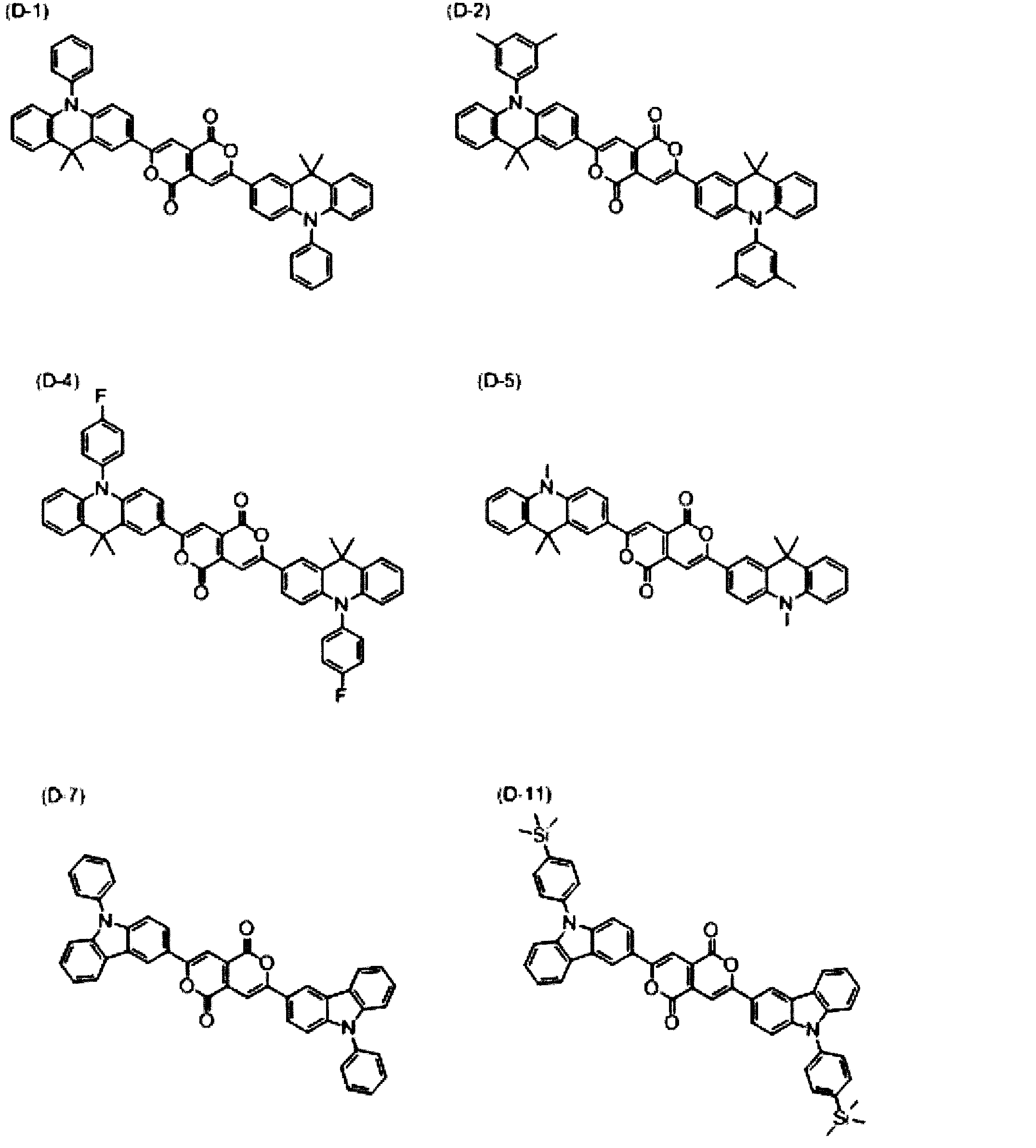
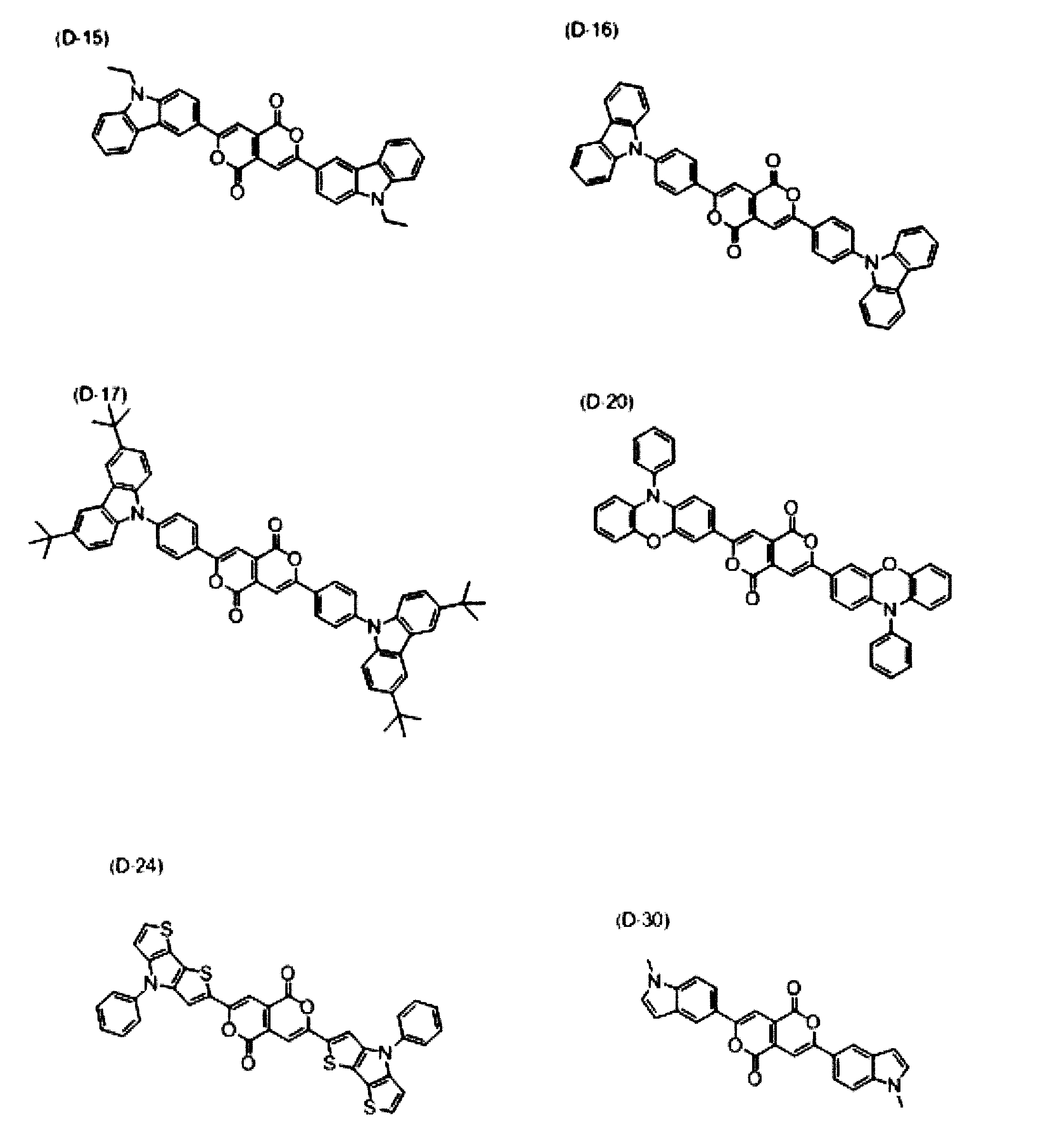

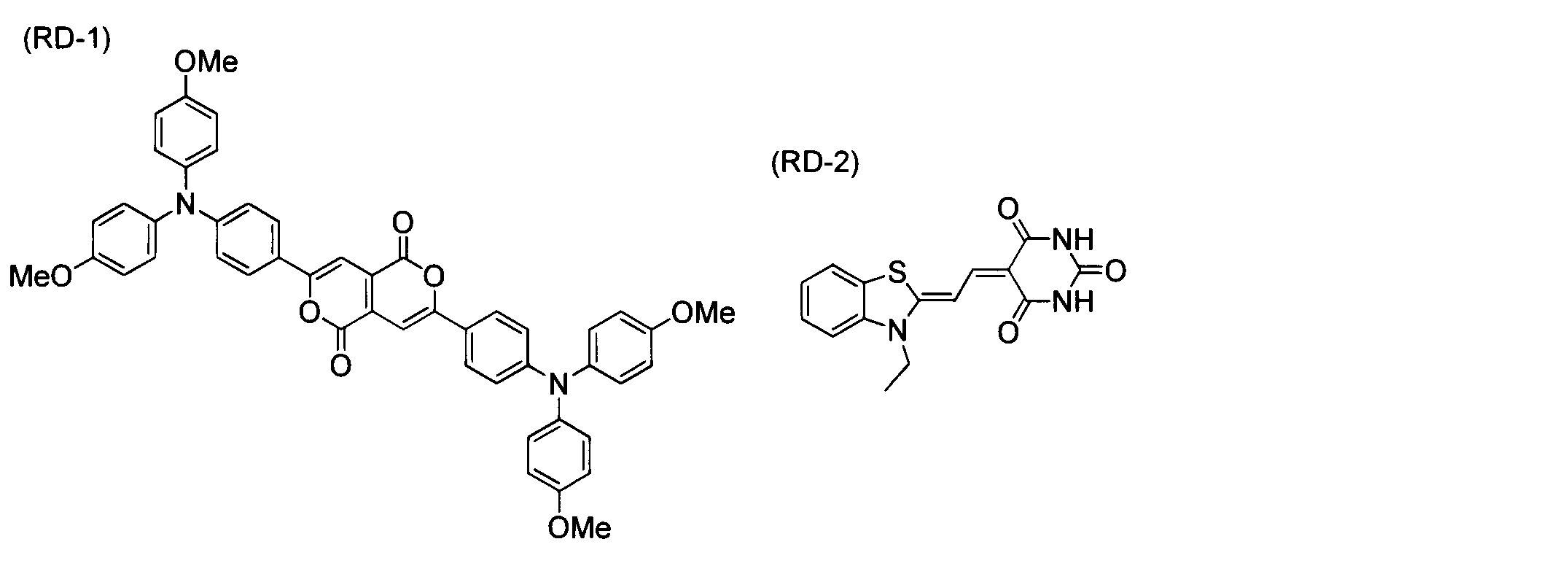
<光電変換素子の作製1(図3の実施態様を想定した素子)>
図3に示したような、光電変換膜がパンクロ感光である実施態様に用いる光電変換素子として、図1(a)の形態の光電変換素子を以下のような条件作製した。ここで、光電変換素子は、下部電極11、電子ブロッキング膜16A、光電変換膜12および上部電極15からなる。
具体的には、ガラス基板上に、アモルファス性ITOをスパッタ法により成膜して、下部電極11(厚み:30nm)を形成し、さらに下部電極11上に下記化合物(EB-1)を真空加熱蒸着法により成膜して、電子ブロッキング膜16A(厚み:100nm)を形成した。さらに、基板の温度を25℃に制御した状態で、電子ブロッキング膜16A上に、上記化合物D-1とフラーレン(C60)とをそれぞれ単層換算で120nm、280nmとなるように真空加熱蒸着により共蒸着して成膜し、光電変換膜12を形成した。さらに、光電変換膜12上に、アモルファス性ITOをスパッタ法により成膜して、上部電極15(透明導電性膜)(厚み:10nm)を形成した。上部電極15上に、加熱蒸着により封止層としてSiO膜を形成した後、その上にALCVD法により酸化アルミニウム(Al2O3)層を形成し、光電変換素子を作製した。
なお、化合物D-1の代わりに、後述する表1に示す化合物を使用した以外は、上記と同様の手順に従って、各光電変換素子を製造した。評価結果は表1に対応する。
図3に示したような、光電変換膜がパンクロ感光である実施態様に用いる光電変換素子として、図1(a)の形態の光電変換素子を以下のような条件作製した。ここで、光電変換素子は、下部電極11、電子ブロッキング膜16A、光電変換膜12および上部電極15からなる。
具体的には、ガラス基板上に、アモルファス性ITOをスパッタ法により成膜して、下部電極11(厚み:30nm)を形成し、さらに下部電極11上に下記化合物(EB-1)を真空加熱蒸着法により成膜して、電子ブロッキング膜16A(厚み:100nm)を形成した。さらに、基板の温度を25℃に制御した状態で、電子ブロッキング膜16A上に、上記化合物D-1とフラーレン(C60)とをそれぞれ単層換算で120nm、280nmとなるように真空加熱蒸着により共蒸着して成膜し、光電変換膜12を形成した。さらに、光電変換膜12上に、アモルファス性ITOをスパッタ法により成膜して、上部電極15(透明導電性膜)(厚み:10nm)を形成した。上部電極15上に、加熱蒸着により封止層としてSiO膜を形成した後、その上にALCVD法により酸化アルミニウム(Al2O3)層を形成し、光電変換素子を作製した。
なお、化合物D-1の代わりに、後述する表1に示す化合物を使用した以外は、上記と同様の手順に従って、各光電変換素子を製造した。評価結果は表1に対応する。

<光電変換素子の作製2(図2の実施態様を想定した素子)>
図2に示したハイブリッド型の実施態様に用いるためのG光選択的な光電変換素子として図1(a)の形態の光電変換素子を以下のような条件で作製した。ここで、光電変換素子は、下部電極11、電子ブロッキング膜16A、光電変換膜12および上部電極15からなる。
具体的には、ガラス基板上に、アモルファス性ITOをスパッタ法により成膜して、下部電極11(厚み:30nm)を形成し、さらに下部電極11上に上記化合物(EB-1)を真空加熱蒸着法により成膜して、電子ブロッキング膜16A(厚み:100nm)を形成した。さらに、基板の温度を25℃に制御した状態で、電子ブロッキング膜16A上に、上記化合物D-1と下記化合物N-1とをそれぞれ単層換算で100nm、100nmとなるように真空加熱蒸着により共蒸着して成膜し、光電変換膜12を形成した。さらに、光電変換膜12上に、アモルファス性ITOをスパッタ法により成膜して、上部電極15(透明導電性膜)(厚み:10nm)を形成した。上部電極15上に、加熱蒸着により封止層としてSiO膜を形成した後、その上にALCVD法により酸化アルミニウム(Al2O3)層を形成し、光電変換素子を作製した。
なお、化合物D-1の代わりに、後述する表2に示す化合物を使用した以外は、上記と同様の手順に従って、各光電変換素子を製造した。評価結果は表2に対応する。
図2に示したハイブリッド型の実施態様に用いるためのG光選択的な光電変換素子として図1(a)の形態の光電変換素子を以下のような条件で作製した。ここで、光電変換素子は、下部電極11、電子ブロッキング膜16A、光電変換膜12および上部電極15からなる。
具体的には、ガラス基板上に、アモルファス性ITOをスパッタ法により成膜して、下部電極11(厚み:30nm)を形成し、さらに下部電極11上に上記化合物(EB-1)を真空加熱蒸着法により成膜して、電子ブロッキング膜16A(厚み:100nm)を形成した。さらに、基板の温度を25℃に制御した状態で、電子ブロッキング膜16A上に、上記化合物D-1と下記化合物N-1とをそれぞれ単層換算で100nm、100nmとなるように真空加熱蒸着により共蒸着して成膜し、光電変換膜12を形成した。さらに、光電変換膜12上に、アモルファス性ITOをスパッタ法により成膜して、上部電極15(透明導電性膜)(厚み:10nm)を形成した。上部電極15上に、加熱蒸着により封止層としてSiO膜を形成した後、その上にALCVD法により酸化アルミニウム(Al2O3)層を形成し、光電変換素子を作製した。
なお、化合物D-1の代わりに、後述する表2に示す化合物を使用した以外は、上記と同様の手順に従って、各光電変換素子を製造した。評価結果は表2に対応する。

<素子駆動の確認(暗電流の測定)>
得られた各素子について光電変換素子として機能するかどうかの確認を行った。
得られた各素子(実施例1~20、比較例1~4)の下部電極および上部電極に、2.5×10⁵V/cmの電界強度となるように電圧を印加すると、いずれの素子も暗所では100nA/cm2以下の暗電流を示すが、明所では10μA/cm2以上の電流を示し、光電変換素子が機能することを確認した。
得られた各素子について光電変換素子として機能するかどうかの確認を行った。
得られた各素子(実施例1~20、比較例1~4)の下部電極および上部電極に、2.5×10⁵V/cmの電界強度となるように電圧を印加すると、いずれの素子も暗所では100nA/cm2以下の暗電流を示すが、明所では10μA/cm2以上の電流を示し、光電変換素子が機能することを確認した。
<応答速度評価(応答性評価)>
得られた各光電変換素子について応答性を評価した。
具体的には、光電変換素子に2.0×10⁵V/cmの電界強度となるように電圧を印加した。その後、LEDを瞬間的に点灯させて上部電極(透明導電性膜)側から光を照射し、そのときの光電流をオシロスコープで測定して、相対応答速度(0から98%信号強度までの立ち上がり時間)を測定した。なお、各素子の応答速度の測定の際には上部電極(透明導電性膜)側から光を入射した。
以下に応答速度(相対値)の求め方を示す。実施例1~17、および比較例1、2に関しては、実施例X(または比較例X)の応答速度(相対値)=[実施例X(または比較例X)における0から98%信号強度への立ち上がり時間/実施例1における0から98%信号強度への立ち上がり時間]。実施例18~20、および比較例3、4に関しては、実施例X(または比較例X)の応答速度(相対値)=[実施例X(または比較例X)における0から98%信号強度への立ち上がり時間/実施例18における0から98%信号強度への立ち上がり時間]。
なお、上記応答速度(相対値)としては、実用上15以下であることが好ましく、5以下であることがより好ましく、2以下であることがさらに好ましい。
得られた各光電変換素子について応答性を評価した。
具体的には、光電変換素子に2.0×10⁵V/cmの電界強度となるように電圧を印加した。その後、LEDを瞬間的に点灯させて上部電極(透明導電性膜)側から光を照射し、そのときの光電流をオシロスコープで測定して、相対応答速度(0から98%信号強度までの立ち上がり時間)を測定した。なお、各素子の応答速度の測定の際には上部電極(透明導電性膜)側から光を入射した。
以下に応答速度(相対値)の求め方を示す。実施例1~17、および比較例1、2に関しては、実施例X(または比較例X)の応答速度(相対値)=[実施例X(または比較例X)における0から98%信号強度への立ち上がり時間/実施例1における0から98%信号強度への立ち上がり時間]。実施例18~20、および比較例3、4に関しては、実施例X(または比較例X)の応答速度(相対値)=[実施例X(または比較例X)における0から98%信号強度への立ち上がり時間/実施例18における0から98%信号強度への立ち上がり時間]。
なお、上記応答速度(相対値)としては、実用上15以下であることが好ましく、5以下であることがより好ましく、2以下であることがさらに好ましい。
<製造適性評価>
各実施例および比較例での光電変換素子の製造適性を比較するために、各光電変換材料を用いて5時間連続蒸着後の応答性の低下を調べた。具体的には以下のとおり評価した。
まず、蒸着レートを3.0Å/秒に固定して連続蒸着を行い、「蒸着開始直後」と「蒸着開始から5時間後」に、上述した光電変換素子の作製と同様の手順に従って光電変換素子を作製した。そして、「蒸着開始直後に作製した素子」および「蒸着開始から5時間後に作製した素子」それぞれについて上述した応答性の評価と同様の手順に従って、0から98%信号強度までの立ち上がり時間を評価し、以下のとおり、応答性の低下を調べた。
応答性の低下=(蒸着開始から5時間後に作製した素子の立ち上がり時間)/(蒸着開始直後に作製した素子の立ち上がり時間)
結果を表1に示す。なお、上記応答性の低下が、1.1未満のものを「AA」、1.1以上1.2未満のものを「A」、1.2以上1.5未満のものを「B」1.5以上3.0未満のものを「C」、3.0以上のものを「D」とした。結果を表1に示す。実用上、「AA」、「A」または「B」であることが好ましく、「AA」または「A」であることがより好ましく、「AA」であることがさらに好ましい。
各実施例および比較例での光電変換素子の製造適性を比較するために、各光電変換材料を用いて5時間連続蒸着後の応答性の低下を調べた。具体的には以下のとおり評価した。
まず、蒸着レートを3.0Å/秒に固定して連続蒸着を行い、「蒸着開始直後」と「蒸着開始から5時間後」に、上述した光電変換素子の作製と同様の手順に従って光電変換素子を作製した。そして、「蒸着開始直後に作製した素子」および「蒸着開始から5時間後に作製した素子」それぞれについて上述した応答性の評価と同様の手順に従って、0から98%信号強度までの立ち上がり時間を評価し、以下のとおり、応答性の低下を調べた。
応答性の低下=(蒸着開始から5時間後に作製した素子の立ち上がり時間)/(蒸着開始直後に作製した素子の立ち上がり時間)
結果を表1に示す。なお、上記応答性の低下が、1.1未満のものを「AA」、1.1以上1.2未満のものを「A」、1.2以上1.5未満のものを「B」1.5以上3.0未満のものを「C」、3.0以上のものを「D」とした。結果を表1に示す。実用上、「AA」、「A」または「B」であることが好ましく、「AA」または「A」であることがより好ましく、「AA」であることがさらに好ましい。
表1中、「分子量」は各実施例および比較例で使用した光電変換材料の分子量を示す。
また、「双極子モーメント」は、各実施例および比較例で使用した光電変換材料の双極子モーメントを示す。
また、「双極子モーメント」は、各実施例および比較例で使用した光電変換材料の双極子モーメントを示す。
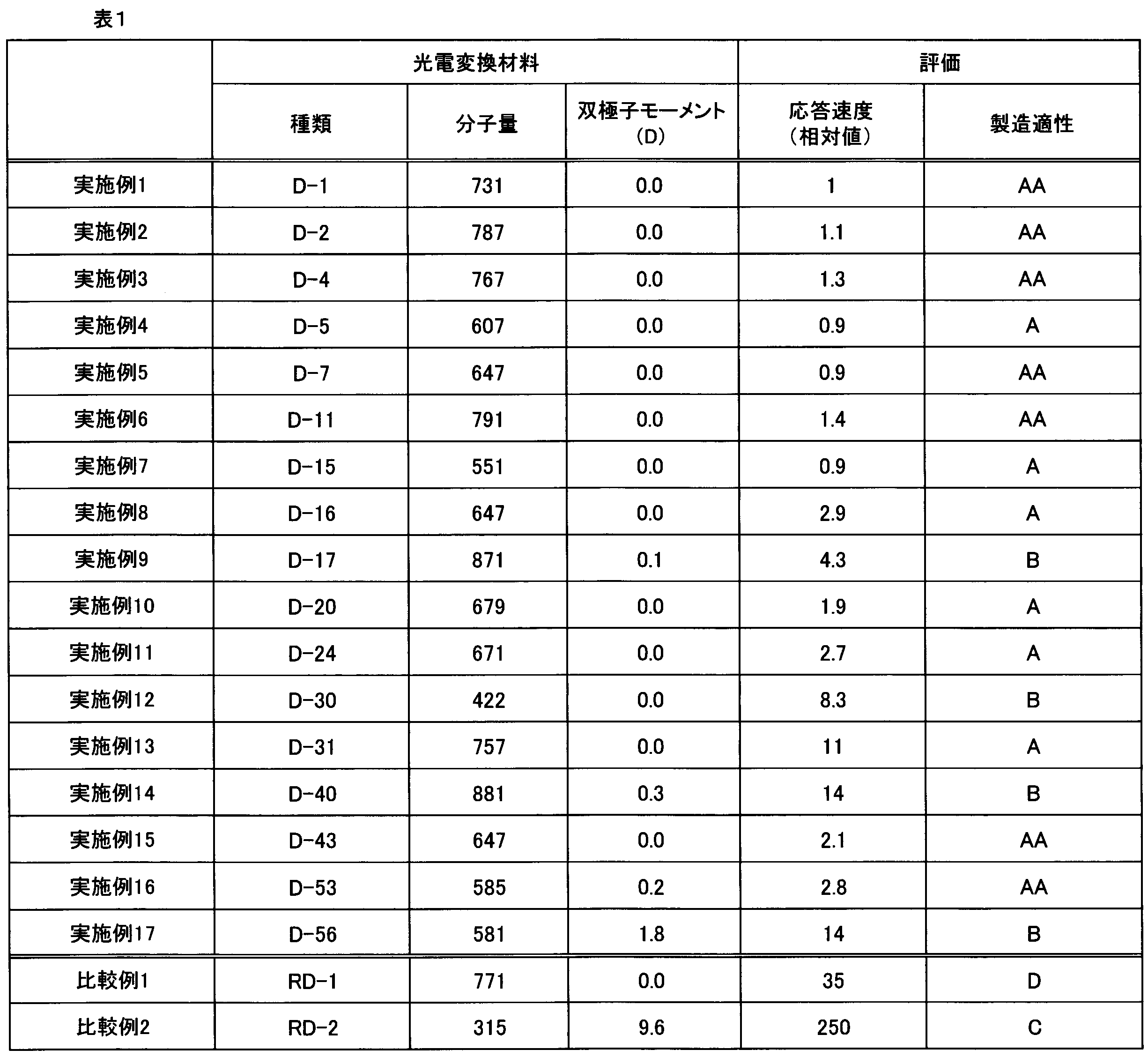
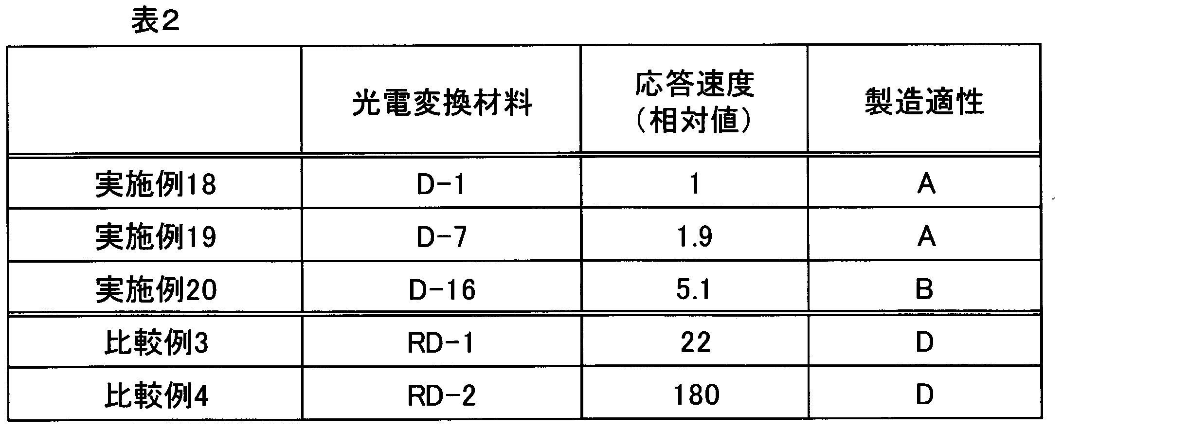
上記表1に示すように、本発明の光電変換素子においては、優れた応答性および製造適性を示すことが確認された。
なかでも、実施例1、実施例13と実施例14との比較から分かるように、X1およびX2がいずれも酸素原子である場合、応答性がより優れることが確認された。
また、実施例5と実施例15との比較から分かるように、一般式(2-1)で表される基を使用する場合、応答性がより優れることが確認された。
また、実施例5と実施例8との比較から分かるように、Ar1とR1、および、Ar2とR3が、それぞれ互いに結合して環を形成する場合、応答性および製造適性がより優れることが確認された。
また、実施例12と他の実施例との比較から分かるように、R1、R2、R3、および、R4のうち環を形成する基が、置換基を有してもよいアリールまたは置換基を有してもよいヘテロアリール基である場合、応答性および製造適性がより優れることが確認された。
また、実施例1、実施例5、および実施例10の比較から分かるように、Ar1とR1、Ar1とR2、R1とR2、Ar2とR3、Ar2とR4およびR3とR4のうち、少なくとも一つがそれぞれ互いに結合して環を形成する場合、直接、または、アルキレン基を介して互いに結合すると、応答性および製造適性がより優れることが確認された。
また、実施例5と実施例11との比較より、R1、R2、R3、および、R4がアリール基である場合、応答性および製造適性がより優れることが確認された。
また、実施例17と他の実施例との比較から分かるように、Ar1とR1、Ar1とR2およびR1とR2の少なくとも一つ、並びに、Ar2とR3、Ar2とR4およびR3とR4の少なくとも一つがそれぞれ互いに結合して環を形成する場合、応答性および製造適性がより優れることが確認された。
また、実施例9、12、14および17と、他の実施例との比較から分かるように、化合物の分子量が500以上850未満で、かつ、化合物の双極子モーメントが1D以下の場合、製造適性がより優れることが確認された。
また、実施例18~20の結果からハイブリッド型での実施態様を想定して、有機n型化合物(n型半導体化合物)を変えた場合にも同様の傾向が確認された。
なかでも、実施例1、実施例13と実施例14との比較から分かるように、X1およびX2がいずれも酸素原子である場合、応答性がより優れることが確認された。
また、実施例5と実施例15との比較から分かるように、一般式(2-1)で表される基を使用する場合、応答性がより優れることが確認された。
また、実施例5と実施例8との比較から分かるように、Ar1とR1、および、Ar2とR3が、それぞれ互いに結合して環を形成する場合、応答性および製造適性がより優れることが確認された。
また、実施例12と他の実施例との比較から分かるように、R1、R2、R3、および、R4のうち環を形成する基が、置換基を有してもよいアリールまたは置換基を有してもよいヘテロアリール基である場合、応答性および製造適性がより優れることが確認された。
また、実施例1、実施例5、および実施例10の比較から分かるように、Ar1とR1、Ar1とR2、R1とR2、Ar2とR3、Ar2とR4およびR3とR4のうち、少なくとも一つがそれぞれ互いに結合して環を形成する場合、直接、または、アルキレン基を介して互いに結合すると、応答性および製造適性がより優れることが確認された。
また、実施例5と実施例11との比較より、R1、R2、R3、および、R4がアリール基である場合、応答性および製造適性がより優れることが確認された。
また、実施例17と他の実施例との比較から分かるように、Ar1とR1、Ar1とR2およびR1とR2の少なくとも一つ、並びに、Ar2とR3、Ar2とR4およびR3とR4の少なくとも一つがそれぞれ互いに結合して環を形成する場合、応答性および製造適性がより優れることが確認された。
また、実施例9、12、14および17と、他の実施例との比較から分かるように、化合物の分子量が500以上850未満で、かつ、化合物の双極子モーメントが1D以下の場合、製造適性がより優れることが確認された。
また、実施例18~20の結果からハイブリッド型での実施態様を想定して、有機n型化合物(n型半導体化合物)を変えた場合にも同様の傾向が確認された。
一方、特許文献1の実施例欄で使用されていたRD-1を使用した場合(比較例1に該当)、および、他の化合物(RD-2)を使用した場合、応答性および製造適性が劣ることが確認された。これは有機n型化合物(n型半導体化合物)を変えた場合にも同様の傾向が確認された。
<撮像素子の作製>
図3に示す形態と同様の撮像素子を作製した。すなわち、CMOS基板上に、アモルファス性TiN 30nmをスパッタ法により成膜後、フォトリソグラフィーによりCMOS基板上のフォトダイオード(PD)の上にそれぞれ1つずつ画素が存在するようにパターニングして下部電極とし、電子ブロッキング材料の成膜以降は実施例1~17、比較例1~2と同様に作製した。その評価も同様に行い、表1と同様な結果が得られ、撮像素子においても製造に適していることと、優れた性能を示すことが分かった。
図3に示す形態と同様の撮像素子を作製した。すなわち、CMOS基板上に、アモルファス性TiN 30nmをスパッタ法により成膜後、フォトリソグラフィーによりCMOS基板上のフォトダイオード(PD)の上にそれぞれ1つずつ画素が存在するようにパターニングして下部電極とし、電子ブロッキング材料の成膜以降は実施例1~17、比較例1~2と同様に作製した。その評価も同様に行い、表1と同様な結果が得られ、撮像素子においても製造に適していることと、優れた性能を示すことが分かった。
10a、10b 光電変換素子
11 下部電極(導電性膜)
12 光電変換膜
15 上部電極(透明導電性膜)
16A 電子ブロッキング膜
16B 正孔ブロッキング膜
100 画素分離型撮像素子
101 基板
102 絶縁層
103 接続電極
104 画素電極(下部電極)
105 接続部
106 接続部
107 光電変換膜
108 対向電極(上部電極)
109 緩衝層
110 封止層
111 カラーフィルタ(CF)
112 隔壁
113 遮光層
114 保護層
115 対向電極電圧供給部
116 読み出し回路
200 光電変換素子(ハイブリッド型の光電変換素子)
201 無機光電変換膜
202 n型ウェル
203 p型ウェル
204 n型ウェル
205 p型シリコン基板
207 絶縁層
208 画素電極
209 有機光電変換膜
210 共通電極
211 保護膜
212 電子ブロッキング膜
11 下部電極(導電性膜)
12 光電変換膜
15 上部電極(透明導電性膜)
16A 電子ブロッキング膜
16B 正孔ブロッキング膜
100 画素分離型撮像素子
101 基板
102 絶縁層
103 接続電極
104 画素電極(下部電極)
105 接続部
106 接続部
107 光電変換膜
108 対向電極(上部電極)
109 緩衝層
110 封止層
111 カラーフィルタ(CF)
112 隔壁
113 遮光層
114 保護層
115 対向電極電圧供給部
116 読み出し回路
200 光電変換素子(ハイブリッド型の光電変換素子)
201 無機光電変換膜
202 n型ウェル
203 p型ウェル
204 n型ウェル
205 p型シリコン基板
207 絶縁層
208 画素電極
209 有機光電変換膜
210 共通電極
211 保護膜
212 電子ブロッキング膜
Claims (12)
- 導電性膜、光電変換材料を含む光電変換膜、および透明導電性膜をこの順で有する光電変換素子であって、
前記光電変換材料が、一般式(1)で表される化合物を含む、光電変換素子。

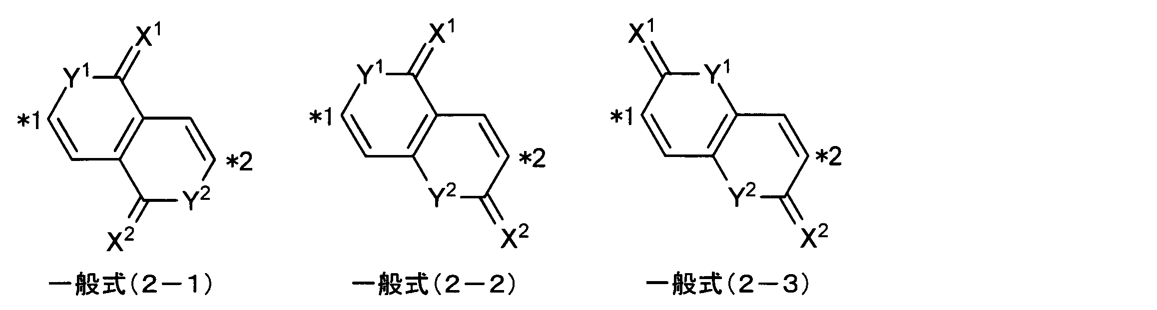
- 一般式(1)中、Ar1とR1、Ar1とR2およびR1とR2の少なくとも一つ、並びに、Ar2とR3、Ar2とR4およびR3とR4の少なくとも一つがそれぞれ互いに結合して環を形成する、請求項1に記載の光電変換素子。
- 一般式(1)中、R1、R2、R3、および、R4のうち前記環を形成する基が、置換基を有してもよいアリール基または置換基を有してもよいヘテロアリール基である、請求項1または2に記載の光電変換素子。
- 一般式(1)中、Ar1とR1、および、Ar2とR3が、それぞれ互いに結合して環を形成する、請求項1~3のいずれか1項に記載の光電変換素子。
- A1が前記一般式(2-1)で表される基である、請求項1~4のいずれか1項に記載の光電変換素子。
- 一般式(1)中、X1およびX2がいずれも酸素原子である、請求項1~5のいずれか1項に記載の光電変換素子。
- 一般式(1)で表される化合物の双極子モーメントが1D以下である、請求項1~6のいずれか1項に記載の光電変換素子。
- 一般式(1)で表される化合物の分子量が500以上850未満である、請求項1~7のいずれか1項に記載の光電変換素子。
- 前記光電変換膜が、さらに有機n型化合物を含む、請求項1~8のいずれか1項に記載の光電変換素子。
- 前記導電性膜と前記透明導電性膜との間に電荷ブロッキング膜が配置される、請求項1~9のいずれか1項に記載の光電変換素子。
- 請求項1~10のいずれか1項に記載の光電変換素子を含む光センサ。
- 請求項1~10のいずれか1項に記載の光電変換素子を含む撮像素子。
Priority Applications (1)
| Application Number | Priority Date | Filing Date | Title |
|---|---|---|---|
| KR1020167016085A KR101777534B1 (ko) | 2014-01-31 | 2015-01-19 | 광전 변환 소자, 촬상 소자, 광 센서 |
Applications Claiming Priority (2)
| Application Number | Priority Date | Filing Date | Title |
|---|---|---|---|
| JP2014016882A JP6047108B2 (ja) | 2014-01-31 | 2014-01-31 | 光電変換素子、撮像素子、光センサ |
| JP2014-016882 | 2014-01-31 |
Publications (1)
| Publication Number | Publication Date |
|---|---|
| WO2015115229A1 true WO2015115229A1 (ja) | 2015-08-06 |
Family
ID=53756806
Family Applications (1)
| Application Number | Title | Priority Date | Filing Date |
|---|---|---|---|
| PCT/JP2015/051224 Ceased WO2015115229A1 (ja) | 2014-01-31 | 2015-01-19 | 光電変換素子、撮像素子、光センサ |
Country Status (4)
| Country | Link |
|---|---|
| JP (1) | JP6047108B2 (ja) |
| KR (1) | KR101777534B1 (ja) |
| TW (1) | TW201529800A (ja) |
| WO (1) | WO2015115229A1 (ja) |
Cited By (4)
| Publication number | Priority date | Publication date | Assignee | Title |
|---|---|---|---|---|
| WO2017126153A1 (ja) * | 2016-01-22 | 2017-07-27 | コニカミノルタ株式会社 | 光学式指紋認証装置 |
| CN109320525A (zh) * | 2018-11-19 | 2019-02-12 | 广东工业大学 | 一种含吩噁嗪结构的双给体空穴传输材料及其制备方法和钙钛矿太阳能电池 |
| WO2020021211A1 (fr) * | 2018-07-27 | 2020-01-30 | Lynred | Dispositif de detection de rayonnement electromagnetique |
| US12439815B2 (en) | 2020-12-30 | 2025-10-07 | Samsung Electronics Co., Ltd. | Blue light absorbing film, and photoelectric device, image sensor and electronic device including the same |
Families Citing this family (5)
| Publication number | Priority date | Publication date | Assignee | Title |
|---|---|---|---|---|
| JP6665430B2 (ja) * | 2015-06-23 | 2020-03-13 | 株式会社リコー | エレクトロクロミック化合物、エレクトロクロミック組成物、及びエレクトロクロミック表示素子 |
| TWI608244B (zh) * | 2015-08-07 | 2017-12-11 | 佳能股份有限公司 | 光電轉換設備、測距裝置、及資訊處理系統 |
| JP6892932B2 (ja) * | 2017-11-17 | 2021-06-23 | 富士フイルム株式会社 | 光電変換素子、光センサ、撮像素子、化合物 |
| CN109928969A (zh) * | 2019-04-15 | 2019-06-25 | 兰州大学 | 萘啶酮类化合物及其制备方法和应用、含氮杂环的药物组合物 |
| WO2024202762A1 (ja) * | 2023-03-24 | 2024-10-03 | 富士フイルム株式会社 | 光電変換素子、撮像素子、光センサ、化合物 |
Citations (1)
| Publication number | Priority date | Publication date | Assignee | Title |
|---|---|---|---|---|
| JP2011199152A (ja) * | 2010-03-23 | 2011-10-06 | Sony Corp | 光電変換素子及び固体撮像装置 |
Family Cites Families (2)
| Publication number | Priority date | Publication date | Assignee | Title |
|---|---|---|---|---|
| JP2006054448A (ja) | 2004-07-16 | 2006-02-23 | Fuji Photo Film Co Ltd | 機能素子及びその製造方法 |
| JP5325473B2 (ja) | 2008-06-20 | 2013-10-23 | 富士フイルム株式会社 | 光電変換素子及び固体撮像素子 |
-
2014
- 2014-01-31 JP JP2014016882A patent/JP6047108B2/ja active Active
-
2015
- 2015-01-19 WO PCT/JP2015/051224 patent/WO2015115229A1/ja not_active Ceased
- 2015-01-19 KR KR1020167016085A patent/KR101777534B1/ko active Active
- 2015-01-28 TW TW104102773A patent/TW201529800A/zh unknown
Patent Citations (1)
| Publication number | Priority date | Publication date | Assignee | Title |
|---|---|---|---|---|
| JP2011199152A (ja) * | 2010-03-23 | 2011-10-06 | Sony Corp | 光電変換素子及び固体撮像装置 |
Non-Patent Citations (1)
| Title |
|---|
| MIKIHIRO HAYASHI ET AL.: "Double Lactonization in Triarylamine-Conjugated Dimethyl Diethynylfumarate: Formation of Intensely Colored and Luminescent Quadrupolar Molecules Including a Missing Structural Isomer of Pechmann Dyes", JOURNAL OF THE AMERICAN CHEMICAL SOCIETY, vol. 133, no. 37, 15 August 2011 (2011-08-15), pages 14518 - 14521, XP055215097 * |
Cited By (12)
| Publication number | Priority date | Publication date | Assignee | Title |
|---|---|---|---|---|
| WO2017126153A1 (ja) * | 2016-01-22 | 2017-07-27 | コニカミノルタ株式会社 | 光学式指紋認証装置 |
| WO2020021211A1 (fr) * | 2018-07-27 | 2020-01-30 | Lynred | Dispositif de detection de rayonnement electromagnetique |
| FR3084523A1 (fr) * | 2018-07-27 | 2020-01-31 | Societe Francaise De Detecteurs Infrarouges - Sofradir | Dispositif de detection electromagnetique |
| KR20210032394A (ko) * | 2018-07-27 | 2021-03-24 | 린레드 | 전자기 방사선을 검출하기 위한 디바이스 |
| CN112740408A (zh) * | 2018-07-27 | 2021-04-30 | 灵锐得 | 电磁辐射检测装置 |
| JP2021533387A (ja) * | 2018-07-27 | 2021-12-02 | リンレッド | 電磁放射検出装置 |
| KR102617508B1 (ko) | 2018-07-27 | 2023-12-22 | 린레드 | 전자기 방사선을 검출하기 위한 디바이스 |
| US11869905B2 (en) | 2018-07-27 | 2024-01-09 | Lynred | Electromagnetic radiation detection device |
| JP7465873B2 (ja) | 2018-07-27 | 2024-04-11 | リンレッド | 電磁放射検出装置 |
| CN109320525A (zh) * | 2018-11-19 | 2019-02-12 | 广东工业大学 | 一种含吩噁嗪结构的双给体空穴传输材料及其制备方法和钙钛矿太阳能电池 |
| CN109320525B (zh) * | 2018-11-19 | 2021-07-06 | 广东工业大学 | 一种含吩噁嗪结构的双给体空穴传输材料及其制备方法和钙钛矿太阳能电池 |
| US12439815B2 (en) | 2020-12-30 | 2025-10-07 | Samsung Electronics Co., Ltd. | Blue light absorbing film, and photoelectric device, image sensor and electronic device including the same |
Also Published As
| Publication number | Publication date |
|---|---|
| TW201529800A (zh) | 2015-08-01 |
| JP2015144187A (ja) | 2015-08-06 |
| KR20160088360A (ko) | 2016-07-25 |
| JP6047108B2 (ja) | 2016-12-21 |
| KR101777534B1 (ko) | 2017-09-11 |
Similar Documents
| Publication | Publication Date | Title |
|---|---|---|
| JP6047108B2 (ja) | 光電変換素子、撮像素子、光センサ | |
| US10559763B2 (en) | Photoelectric conversion element, imaging device, optical sensor, and method of using photoelectric conversion element | |
| KR101719089B1 (ko) | 광전 변환 소자 및 그 사용 방법, 광 센서, 촬상 소자 | |
| JP5925234B2 (ja) | 光電変換材料、光電変換素子およびその使用方法、光センサ、撮像素子 | |
| TWI618699B (zh) | 光電轉換材料、光電轉換元件、光感測器及攝像元件 | |
| WO2018186389A1 (ja) | 光電変換素子、光センサ、および、撮像素子 | |
| JP6535093B2 (ja) | 光電変換素子、撮像素子、光センサ、化合物 | |
| WO2015025717A1 (ja) | 光電変換素子、光センサおよび撮像素子 | |
| JP6077426B2 (ja) | 光電変換素子およびその使用方法、光センサ、撮像素子 | |
| JP6675005B2 (ja) | 光電変換素子、撮像素子、光センサ、化合物 | |
| WO2018105269A1 (ja) | 光電変換素子、光センサ、及び、撮像素子 | |
| JP2013012535A (ja) | 光電変換素子およびその使用方法、撮像素子、光センサ、光電変換膜 | |
| JP6674547B2 (ja) | 光電変換素子、撮像素子、光センサ、化合物 | |
| JP6684908B2 (ja) | 光電変換素子、撮像素子、光センサ、化合物 | |
| WO2014157009A1 (ja) | 光電変換素子、撮像素子、光センサ | |
| JP5890366B2 (ja) | 光電変換素子、撮像素子、光センサ | |
| JP6114606B2 (ja) | 光電変換材料、光電変換素子およびその使用方法、光センサ、撮像素子 |
Legal Events
| Date | Code | Title | Description |
|---|---|---|---|
| 121 | Ep: the epo has been informed by wipo that ep was designated in this application |
Ref document number: 15743401 Country of ref document: EP Kind code of ref document: A1 |
|
| ENP | Entry into the national phase |
Ref document number: 20167016085 Country of ref document: KR Kind code of ref document: A |
|
| NENP | Non-entry into the national phase |
Ref country code: DE |
|
| 122 | Ep: pct application non-entry in european phase |
Ref document number: 15743401 Country of ref document: EP Kind code of ref document: A1 |