WO2015114863A1 - 実装基板の製造装置、及び実装基板の製造方法 - Google Patents
実装基板の製造装置、及び実装基板の製造方法 Download PDFInfo
- Publication number
- WO2015114863A1 WO2015114863A1 PCT/JP2014/072432 JP2014072432W WO2015114863A1 WO 2015114863 A1 WO2015114863 A1 WO 2015114863A1 JP 2014072432 W JP2014072432 W JP 2014072432W WO 2015114863 A1 WO2015114863 A1 WO 2015114863A1
- Authority
- WO
- WIPO (PCT)
- Prior art keywords
- substrate
- driver
- mounting
- fixed
- mounting component
- Prior art date
- Legal status (The legal status is an assumption and is not a legal conclusion. Google has not performed a legal analysis and makes no representation as to the accuracy of the status listed.)
- Ceased
Links
Images










Classifications
-
- H—ELECTRICITY
- H05—ELECTRIC TECHNIQUES NOT OTHERWISE PROVIDED FOR
- H05K—PRINTED CIRCUITS; CASINGS OR CONSTRUCTIONAL DETAILS OF ELECTRIC APPARATUS; MANUFACTURE OF ASSEMBLAGES OF ELECTRICAL COMPONENTS
- H05K3/00—Apparatus or processes for manufacturing printed circuits
- H05K3/36—Assembling printed circuits with other printed circuits
- H05K3/361—Assembling flexible printed circuits with other printed circuits
-
- H—ELECTRICITY
- H05—ELECTRIC TECHNIQUES NOT OTHERWISE PROVIDED FOR
- H05K—PRINTED CIRCUITS; CASINGS OR CONSTRUCTIONAL DETAILS OF ELECTRIC APPARATUS; MANUFACTURE OF ASSEMBLAGES OF ELECTRICAL COMPONENTS
- H05K1/00—Printed circuits
- H05K1/18—Printed circuits structurally associated with non-printed electric components
- H05K1/189—Printed circuits structurally associated with non-printed electric components characterised by the use of flexible or folded printed circuits
-
- H—ELECTRICITY
- H05—ELECTRIC TECHNIQUES NOT OTHERWISE PROVIDED FOR
- H05K—PRINTED CIRCUITS; CASINGS OR CONSTRUCTIONAL DETAILS OF ELECTRIC APPARATUS; MANUFACTURE OF ASSEMBLAGES OF ELECTRICAL COMPONENTS
- H05K2201/00—Indexing scheme relating to printed circuits covered by H05K1/00
- H05K2201/10—Details of components or other objects attached to or integrated in a printed circuit board
- H05K2201/10007—Types of components
- H05K2201/10128—Display
- H05K2201/10136—Liquid Crystal display [LCD]
-
- H—ELECTRICITY
- H05—ELECTRIC TECHNIQUES NOT OTHERWISE PROVIDED FOR
- H05K—PRINTED CIRCUITS; CASINGS OR CONSTRUCTIONAL DETAILS OF ELECTRIC APPARATUS; MANUFACTURE OF ASSEMBLAGES OF ELECTRICAL COMPONENTS
- H05K3/00—Apparatus or processes for manufacturing printed circuits
- H05K3/30—Assembling printed circuits with electric components, e.g. with resistors
- H05K3/32—Assembling printed circuits with electric components, e.g. with resistors electrically connecting electric components or wires to printed circuits
- H05K3/321—Assembling printed circuits with electric components, e.g. with resistors electrically connecting electric components or wires to printed circuits by conductive adhesives
- H05K3/323—Assembling printed circuits with electric components, e.g. with resistors electrically connecting electric components or wires to printed circuits by conductive adhesives by applying an anisotropic conductive adhesive layer over an array of pads
-
- H—ELECTRICITY
- H10—SEMICONDUCTOR DEVICES; ELECTRIC SOLID-STATE DEVICES NOT OTHERWISE PROVIDED FOR
- H10W—GENERIC PACKAGES, INTERCONNECTIONS, CONNECTORS OR OTHER CONSTRUCTIONAL DETAILS OF DEVICES COVERED BY CLASS H10
- H10W72/00—Interconnections or connectors in packages
- H10W72/01—Manufacture or treatment
- H10W72/0198—Manufacture or treatment batch processes
-
- H—ELECTRICITY
- H10—SEMICONDUCTOR DEVICES; ELECTRIC SOLID-STATE DEVICES NOT OTHERWISE PROVIDED FOR
- H10W—GENERIC PACKAGES, INTERCONNECTIONS, CONNECTORS OR OTHER CONSTRUCTIONAL DETAILS OF DEVICES COVERED BY CLASS H10
- H10W72/00—Interconnections or connectors in packages
- H10W72/071—Connecting or disconnecting
- H10W72/0711—Apparatus therefor
-
- H—ELECTRICITY
- H10—SEMICONDUCTOR DEVICES; ELECTRIC SOLID-STATE DEVICES NOT OTHERWISE PROVIDED FOR
- H10W—GENERIC PACKAGES, INTERCONNECTIONS, CONNECTORS OR OTHER CONSTRUCTIONAL DETAILS OF DEVICES COVERED BY CLASS H10
- H10W72/00—Interconnections or connectors in packages
- H10W72/071—Connecting or disconnecting
- H10W72/0711—Apparatus therefor
- H10W72/07141—Means for applying energy, e.g. ovens or lasers
-
- H—ELECTRICITY
- H10—SEMICONDUCTOR DEVICES; ELECTRIC SOLID-STATE DEVICES NOT OTHERWISE PROVIDED FOR
- H10W—GENERIC PACKAGES, INTERCONNECTIONS, CONNECTORS OR OTHER CONSTRUCTIONAL DETAILS OF DEVICES COVERED BY CLASS H10
- H10W72/00—Interconnections or connectors in packages
- H10W72/071—Connecting or disconnecting
- H10W72/072—Connecting or disconnecting of bump connectors
- H10W72/07231—Techniques
- H10W72/07232—Compression bonding, e.g. thermocompression bonding
-
- H—ELECTRICITY
- H10—SEMICONDUCTOR DEVICES; ELECTRIC SOLID-STATE DEVICES NOT OTHERWISE PROVIDED FOR
- H10W—GENERIC PACKAGES, INTERCONNECTIONS, CONNECTORS OR OTHER CONSTRUCTIONAL DETAILS OF DEVICES COVERED BY CLASS H10
- H10W72/00—Interconnections or connectors in packages
- H10W72/071—Connecting or disconnecting
- H10W72/073—Connecting or disconnecting of die-attach connectors
- H10W72/07331—Connecting techniques
- H10W72/07332—Compression bonding, e.g. thermocompression bonding
-
- H—ELECTRICITY
- H10—SEMICONDUCTOR DEVICES; ELECTRIC SOLID-STATE DEVICES NOT OTHERWISE PROVIDED FOR
- H10W—GENERIC PACKAGES, INTERCONNECTIONS, CONNECTORS OR OTHER CONSTRUCTIONAL DETAILS OF DEVICES COVERED BY CLASS H10
- H10W72/00—Interconnections or connectors in packages
- H10W72/071—Connecting or disconnecting
- H10W72/073—Connecting or disconnecting of die-attach connectors
- H10W72/07331—Connecting techniques
- H10W72/07337—Connecting techniques using a polymer adhesive, e.g. an adhesive based on silicone or epoxy
- H10W72/07338—Connecting techniques using a polymer adhesive, e.g. an adhesive based on silicone or epoxy hardening the adhesive by curing, e.g. thermosetting
-
- H—ELECTRICITY
- H10—SEMICONDUCTOR DEVICES; ELECTRIC SOLID-STATE DEVICES NOT OTHERWISE PROVIDED FOR
- H10W—GENERIC PACKAGES, INTERCONNECTIONS, CONNECTORS OR OTHER CONSTRUCTIONAL DETAILS OF DEVICES COVERED BY CLASS H10
- H10W72/00—Interconnections or connectors in packages
- H10W72/071—Connecting or disconnecting
- H10W72/074—Connecting or disconnecting of anisotropic conductive adhesives
-
- H—ELECTRICITY
- H10—SEMICONDUCTOR DEVICES; ELECTRIC SOLID-STATE DEVICES NOT OTHERWISE PROVIDED FOR
- H10W—GENERIC PACKAGES, INTERCONNECTIONS, CONNECTORS OR OTHER CONSTRUCTIONAL DETAILS OF DEVICES COVERED BY CLASS H10
- H10W72/00—Interconnections or connectors in packages
- H10W72/20—Bump connectors, e.g. solder bumps or copper pillars; Dummy bumps; Thermal bumps
- H10W72/261—Functions other than electrical connecting
-
- H—ELECTRICITY
- H10—SEMICONDUCTOR DEVICES; ELECTRIC SOLID-STATE DEVICES NOT OTHERWISE PROVIDED FOR
- H10W—GENERIC PACKAGES, INTERCONNECTIONS, CONNECTORS OR OTHER CONSTRUCTIONAL DETAILS OF DEVICES COVERED BY CLASS H10
- H10W74/00—Encapsulations, e.g. protective coatings
- H10W74/10—Encapsulations, e.g. protective coatings characterised by their shape or disposition
- H10W74/15—Encapsulations, e.g. protective coatings characterised by their shape or disposition on active surfaces of flip-chip devices, e.g. underfills
-
- H—ELECTRICITY
- H10—SEMICONDUCTOR DEVICES; ELECTRIC SOLID-STATE DEVICES NOT OTHERWISE PROVIDED FOR
- H10W—GENERIC PACKAGES, INTERCONNECTIONS, CONNECTORS OR OTHER CONSTRUCTIONAL DETAILS OF DEVICES COVERED BY CLASS H10
- H10W90/00—Package configurations
- H10W90/701—Package configurations characterised by the relative positions of pads or connectors relative to package parts
- H10W90/721—Package configurations characterised by the relative positions of pads or connectors relative to package parts of bump connectors
- H10W90/724—Package configurations characterised by the relative positions of pads or connectors relative to package parts of bump connectors between a chip and a stacked insulating package substrate, interposer or RDL
-
- H—ELECTRICITY
- H10—SEMICONDUCTOR DEVICES; ELECTRIC SOLID-STATE DEVICES NOT OTHERWISE PROVIDED FOR
- H10W—GENERIC PACKAGES, INTERCONNECTIONS, CONNECTORS OR OTHER CONSTRUCTIONAL DETAILS OF DEVICES COVERED BY CLASS H10
- H10W90/00—Package configurations
- H10W90/701—Package configurations characterised by the relative positions of pads or connectors relative to package parts
- H10W90/731—Package configurations characterised by the relative positions of pads or connectors relative to package parts of die-attach connectors
- H10W90/734—Package configurations characterised by the relative positions of pads or connectors relative to package parts of die-attach connectors between a chip and a stacked insulating package substrate, interposer or RDL
-
- H—ELECTRICITY
- H10—SEMICONDUCTOR DEVICES; ELECTRIC SOLID-STATE DEVICES NOT OTHERWISE PROVIDED FOR
- H10W—GENERIC PACKAGES, INTERCONNECTIONS, CONNECTORS OR OTHER CONSTRUCTIONAL DETAILS OF DEVICES COVERED BY CLASS H10
- H10W99/00—Subject matter not provided for in other groups of this subclass
Definitions
- the present invention relates to a mounting board manufacturing apparatus and a mounting board manufacturing method.
- Display devices equipped with a display panel such as a liquid crystal panel are used for portable electronic devices such as mobile phones, smartphones, and notebook computers.
- a display device includes a display panel having a display unit for displaying an image, and a semiconductor that drives the display panel by supplying an output signal generated by processing an input signal supplied from a signal supply source to the display unit.
- a chip As described above, in a display device that is generally classified into small and medium size, as a semiconductor chip mounting method, a COG (Chip On Glass) mounting technique in which a semiconductor chip is directly mounted in an area outside the display portion of the display panel. Is preferably used.
- COG Chip On Glass
- Patent Document 1 described above describes a thermocompression bonding apparatus including a pair of thermocompression bonding heads that pressurize a liquid crystal panel and a TCP mounted on the liquid crystal panel. According to this thermocompression bonding apparatus, the liquid crystal panel and the TCP are heated while separately controlling the temperature according to the respective thermal expansion conditions, thereby facilitating the alignment of the TCP with respect to the liquid crystal panel and the fine pattern in the TCP. I am trying to make a connection.
- thermocompression bonding mounting apparatus in addition to the necessity of providing a pulse heater for heating each of the pair of thermocompression bonding heads, the pair of thermocompression bonding heads are moved up and down, respectively. Therefore, there is a problem that the structure is complicated and the whole thermocompression bonding apparatus tends to be large and the cost of the thermocompression mounting apparatus itself is high.
- a thermocompression bonding head is provided only on the TCP side and the substrate side of the liquid crystal panel is received by a fixed substrate receiving portion, the TCP and the liquid crystal panel are thinned. Further, there has been a problem that warpage is likely to occur due to the difference between the expansion / contraction amount of the TCP caused by heat applied during mounting and the expansion / contraction amount of the liquid crystal panel.
- the present invention has been completed based on the above circumstances, and an object thereof is to suppress the occurrence of warping.
- the mounting substrate manufacturing apparatus of the present invention supports a mounting component mounted on a substrate from the opposite side of the substrate, and a fixed mounting component support portion fixed in the overlapping direction of the substrate and the mounting component.
- the substrate is disposed on the opposite side to the fixed mounting component support portion with respect to the substrate, and is moved to approach the overlapping direction with respect to the fixed mounting component support portion, thereby heating the substrate while applying pressure.
- a movable substrate heating unit capable of performing the above.
- the mounting component is supported from the side opposite to the substrate by the fixed mounting component support portion fixed in the overlapping direction of the substrate and the mounting component, and the movable substrate is supported with respect to the fixed mounting component support portion.
- the heating unit By moving the heating unit so as to approach the overlapping direction, it is possible to heat the substrate while pressing it, thereby mounting the mounting component on the substrate.
- the mounting component is made of silicon or the like and has a relatively high thermal conductivity
- the substrate is made of glass or the like and has a relatively low thermal conductivity.
- the substrate is heated by the movable substrate heating unit while the mounting component is supported by the fixed mounting component support unit whose position is fixed in the overlapping direction, so that the thermal conductivity is relatively high.
- the difference in the amount of thermal expansion and contraction that can occur between the low substrate and the mounting component having a relatively high thermal conductivity is alleviated.
- the movable substrate heating unit is configured to pressurize the substrate by being moved so as to approach the fixed mounting component support unit, a configuration in which a pair of thermocompression bonding heads are raised and lowered as in the past. Compared to the above, the structure of the manufacturing apparatus can be simplified and miniaturized and the cost can be reduced.
- the movable substrate heating portion is configured so that the amount of heat applied to the substrate is the fixed mounting component. It is comprised so that it may become more than the calorie
- a plurality of the movable substrate heating units are provided, a plurality of the movable substrate heating units are provided so as to be slidable in a direction along the plate surface of the substrate. ing.
- a plurality of movable types supported by the slide support unit according to the number and arrangement of the mounting parts on the board.
- the fixed mounting component support portion is made of a light-transmitting material, whereas the curing light irradiation portion is arranged at least on the opposite side of the substrate with respect to the fixed mounting component support portion.
- the fixed mounting component support portion does not require high mechanical strength and high thermal conductivity unlike the movable substrate heating portion, it can be made of a translucent material.
- the curing light from the curing light irradiation part is a fixed type made of a translucent material.
- the anisotropic conductive film that is interposed between the substrate and the mounting component and contains the photocurable resin is efficiently irradiated. Therefore, if the curing light irradiation unit is disposed on the side opposite to the fixed mounting component support unit with respect to the substrate, if the substrate is provided with a light shielding material such as a metal wiring, the curing light is shielded by the light shielding material.
- the irradiation efficiency of the curing light to the anisotropic conductive film is higher.
- an anisotropic conductive film can be hardened in a shorter time, and the tact time concerning mounting of mounting components can be shortened.
- the curing of the anisotropic conductive film is promoted by heating the anisotropic conductive film through the substrate by the movable substrate heating unit, the tact time for mounting the mounting component can be further shortened. .
- the movable substrate heating unit is configured to selectively pressurize and heat a component mounting unit on which the mounted component is mounted in the substrate, and the movable substrate heating is performed on the substrate.
- a board holding part that holds the main board part of the board excluding the component mounting part. In this way, by holding the board main part of the board by the board holding part, it is possible to fix the arrangement of the entire board including the part mounting part, so that the component on which the mounting part is mounted among the boards
- the mounting part can be more stably pressurized by the movable substrate heating part. As a result, unevenness is less likely to occur due to the pressure applied to the component mounting part of the substrate from the movable substrate heating part, and therefore, mounting defects are less likely to occur.
- a method for manufacturing a mounting board according to the present invention includes a temporary pressing step of temporarily pressing a mounting component on a board, and the mounting component temporarily pressed on the board. And the mounting component support portion fixed in the overlapping direction of the mounting component, with the fixed mounting component support portion being supported from the opposite side to the substrate, and disposed on the opposite side of the fixed mounting component support portion with respect to the substrate.
- a crimping step is a temporary pressing step of temporarily pressing a mounting component on a board, and the mounting component temporarily pressed on the board.
- the mounting component temporarily bonded onto the substrate through the pre-bonding process is supported from the opposite side of the substrate by the fixed mounting component support portion fixed in the overlapping direction of the substrate and the mounting component in the main bonding process.
- the mounting component is finally pressure-bonded onto the substrate by heating the substrate while being pressurized by a movable substrate heating unit that is movable so as to approach the fixed mounting component support unit in the overlapping direction.
- the mounting component is made of silicon or the like and has a relatively high thermal conductivity
- the substrate is made of glass or the like and has a relatively low thermal conductivity.
- the substrate is heated by the movable substrate heating unit while the mounting component is supported by the fixed mounting component support unit whose position is fixed in the overlapping direction, so that the thermal conductivity is relatively high.
- the difference in the amount of thermal expansion and contraction that can occur between the low substrate and the mounting component having a relatively high thermal conductivity is alleviated.
- a manufacturing apparatus configured to pressurize the substrate is used. The structure of the manufacturing apparatus can be simplified and reduced in size and the cost can be reduced as compared with the case where the manufacturing apparatus configured to raise and lower the thermocompression bonding head is used.
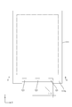
- FIG. 1 is a schematic plan view showing a connection configuration of a liquid crystal panel, a flexible substrate, and a control circuit board on which a driver according to Embodiment 1 of the present invention is mounted.
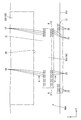
- Schematic sectional view showing the sectional structure of the liquid crystal panel The enlarged plan view which shows the mounting area of the driver and flexible substrate in the array substrate which comprises a liquid crystal panel
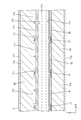
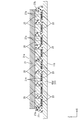
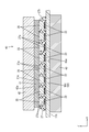
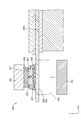
- AA line sectional view of FIG. BB sectional view of FIG. 4 is a cross-sectional view taken along line AA in FIG. 4 showing the operation of the movable substrate heating unit of the driver mounting apparatus.
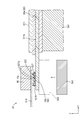
- 4 is a cross-sectional view taken along the line BB in FIG.
- 4 showing the operation of the movable substrate heating unit of the driver mounting apparatus.
- 4 is a cross-sectional view taken along line AA of FIG. 4 showing a state where the driver is mounted by pressing and heating the glass substrate by the movable substrate heating unit of the driver mounting apparatus.
- 4 is a cross-sectional view taken along the line BB of FIG. 4 showing a state in which the driver is mounted by pressurizing and heating the glass substrate by the movable substrate heating unit of the driver mounting apparatus.
- a graph showing the warped state of the driver mounting portion when the main crimping process is performed using the driver mounting apparatus according to the comparative example of the comparative experiment A graph representing the warped state of the driver mounting portion when the main crimping process is performed using the driver mounting apparatus according to the comparative experiment example
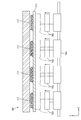
- CC sectional view taken along the line CC in FIG. 13 showing the operation of the movable substrate heating unit of the driver mounting apparatus.
- Top view of a liquid crystal panel with three drivers mounted 15 is a cross-sectional view taken along the line CC of FIG. 15 showing the operation of the movable substrate heating unit of the driver mounting apparatus.
- FIG. 21 DD sectional view of FIG. 21 showing the operation of the movable substrate heating unit of the flexible substrate mounting apparatus.
- FIGS. 1 A first embodiment of the present invention will be described with reference to FIGS.
- a method for manufacturing a liquid crystal panel (display panel) 11 constituting the liquid crystal display device 10 and a driver mounting device (manufacturing device) 40 used for the manufacture will be exemplified.
- a part of each drawing shows an X axis, a Y axis, and a Z axis, and each axis direction is drawn to be a direction shown in each drawing. 2 and 3, the upper side of the figure is the front side and the lower side of the figure is the back side.
- the liquid crystal display device 10 includes a liquid crystal panel 11, a driver (mounted component) 21 that is mounted on the liquid crystal panel 11 and drives the liquid crystal panel 11, and various input signals to the driver 21.
- a backlight device (illumination device) 14 that is an external light source for supplying the light.
- the liquid crystal display device 10 also includes a pair of front and back exterior members 15 and 16 for housing and holding the liquid crystal panel 11 and the backlight device 14 assembled to each other.
- the liquid crystal display device 10 includes a portable information terminal (including an electronic book and a PDA), a mobile phone (including a smartphone), a notebook computer (including a tablet notebook computer), a digital photo frame, It is used for various electronic devices (not shown) such as portable game machines and electronic ink paper. For this reason, the screen size of the liquid crystal panel 11 constituting the liquid crystal display device 10 is set to about several inches to several tens of inches, and is generally classified into a small size and a small size.
- the backlight device 14 includes a chassis 14a having a substantially box shape that opens toward the front side (the liquid crystal panel 11 side), and a light source (not shown) disposed in the chassis 14a (for example, a cold cathode tube, LED, organic EL, etc.) and an optical member (not shown) arranged so as to cover the opening of the chassis 14a.
- the optical member has a function of converting light emitted from the light source into a planar shape.
- the liquid crystal panel 11 has a vertically long rectangular shape (rectangular shape) as a whole, and an image is located at a position offset toward one end side (upper side in FIG. 1) in the long side direction.
- Display area (active area) AA is arranged, and the driver 21 and the flexible substrate 13 are respectively attached to the other end side in the long side direction (the lower side shown in FIG. 1).
- an area outside the display area AA is a non-display area (non-active area) NAA in which no image is displayed, and a part of the non-display area NAA is a mounting area for the driver 21 and the flexible substrate 13. Yes.
- a frame-shaped one-dot chain line that is slightly smaller than the CF substrate 11a represents the outer shape of the display area AA, and an area outside the one-dot chain line is a non-display area NAA.
- the liquid crystal panel 11 is interposed between a pair of transparent (excellent light-transmitting) substrates 11a and 11b and both the substrates 11a and 11b, and its optical characteristics change as an electric field is applied.
- a liquid crystal layer 11c containing liquid crystal molecules as a substance, and both substrates 11a and 11b are bonded together by a sealing agent (not shown) while maintaining a cell gap corresponding to the thickness of the liquid crystal layer 11c.
- Both the substrates 11a and 11b each include a glass substrate (substrate) GS made of alkali-free glass, quartz glass, or the like, and a plurality of films are laminated on each glass substrate GS by a known photolithography method or the like. It is said.
- the front side is a CF substrate (counter substrate) 11a
- the back side is an array substrate (mounting substrate, element substrate, active matrix substrate) 11b
- the CF substrate 11a has a short side dimension substantially equal to that of the array substrate 11b as shown in FIGS. 1 and 2, but the long side dimension is smaller than that of the array substrate 11b. It is bonded to 11b with one end (upper side shown in FIG. 1) in the long side direction aligned. Therefore, the other end (the lower side shown in FIG.
- the configuration existing in the display area AA in the array substrate 11b and the CF substrate 11a will be briefly described.
- the TFTs 17 and the pixel electrodes 18 are provided side by side in a matrix, and are arranged around the TFTs 17 and the pixel electrodes 18 so as to surround a gate wiring and a source wiring (both not shown).
- the TFT 17 and the pixel electrode 18 are arranged in parallel in a matrix form at the intersection of the gate wiring and the source wiring forming a lattice shape.
- the gate wiring and the source wiring are connected to the gate electrode and the source electrode of the TFT 17, respectively, and the pixel electrode 18 is connected to the drain electrode of the TFT 17.
- the pixel electrode 18 has a vertically long rectangular shape (rectangular shape) when seen in a plan view, and is made of a transparent electrode material such as ITO (IndiumInTin Oxide) or ZnO (Zinc Oxide).
- the array substrate 11b can be provided with a capacitor wiring (not shown) that is parallel to the gate wiring and that crosses the pixel electrode 18.
- the CF substrate 11a has colored portions such as R (red), G (green), and B (blue) as viewed in plan with the pixel electrodes 18 on the array substrate 11b side.
- a large number of color filters 11h are arranged in parallel so as to overlap each other.
- a substantially lattice-shaped light shielding layer (black matrix) 11i for preventing color mixture is formed between each colored portion constituting the color filter 11h.
- the light shielding layer 11i is arranged so as to overlap the above-described gate wiring and source wiring in a plan view.
- a solid counter electrode 11j facing the pixel electrode 18 on the array substrate 11b side is provided on the surface of the color filter 11h and the light shielding layer 11i.
- one display pixel which is a display unit by a set of three colored portions of R (red), G (green), and B (blue) and three pixel electrodes 18 facing them. Is configured.
- the display pixel includes a red pixel having an R colored portion, a green pixel having a G colored portion, and a blue pixel having a B colored portion.
- the pixels of each color constitute a pixel group by being repeatedly arranged along the row direction (X-axis direction) on the plate surface of the liquid crystal panel 11, and this pixel group constitutes the column direction (Y-axis direction). Many are arranged side by side.
- the control circuit board 12 is attached to the back surface of the chassis 14a (the outer surface opposite to the liquid crystal panel 11 side) of the backlight device 14 with screws or the like.
- the control circuit board 12 is mounted with electronic components for supplying various input signals to the driver 21 on a board made of paper phenol or glass epoxy resin, and wiring (conductive path) of a predetermined pattern (not shown) is provided. Routed formation.
- One end (one end side) of the flexible substrate 13 is electrically and mechanically connected to the control circuit board 12 via an ACF (Anisotropic Conductive Film) (not shown).
- the flexible substrate (FPC substrate) 13 includes a base material made of a synthetic resin material (for example, polyimide resin) having insulating properties and flexibility, and a large number of wirings are provided on the base material. It has a pattern (not shown), and one end in the length direction is connected to the control circuit board 12 arranged on the back side of the chassis 14a as described above, while the other end Since the portion (the other end side) is connected to the array substrate 11 b in the liquid crystal panel 11, the liquid crystal display device 10 is bent in a folded shape so that the cross-sectional shape is substantially U-shaped.
- a synthetic resin material for example, polyimide resin
- the wiring pattern is exposed to the outside to form terminal portions (not shown), and these terminal portions are respectively connected to the control circuit board 12 and the liquid crystal panel 11. Are electrically connected to each other. Thereby, an input signal supplied from the control circuit board 12 side can be transmitted to the liquid crystal panel 11 side.
- the driver 21 is composed of an LSI chip having a drive circuit therein, and operates based on a signal supplied from a control circuit board 12 that is a signal supply source. An input signal supplied from the control circuit board 12 is processed to generate an output signal, and the output signal is output toward the display area AA of the liquid crystal panel 11.
- the LSI chip constituting the driver 21 is formed by forming wirings and elements on a silicon wafer containing silicon with high purity.
- the driver 21 has a horizontally long shape when viewed from above, that is, has a long shape along the short side of the liquid crystal panel 11.
- the driver 21 is directly mounted on the non-display area NAA of the array substrate 11b in the liquid crystal panel 11, that is, COG (Chip On On Glass).
- the long side direction (longitudinal direction) of the driver 21 coincides with the X-axis direction (short side direction of the liquid crystal panel 11), and the short side direction (direction orthogonal to the longitudinal direction) is the Y-axis direction (of the liquid crystal panel 11). (Long side direction).
- the connection structure of the flexible substrate 13 and the driver 21 to the non-display area NAA of the array substrate 11b will be described.
- the end portions of the driver 21 and the flexible substrate 13 are respectively attached to the non-overlapping portion that does not overlap the CF substrate 11 a in the non-display area NAA of the array substrate 11 b.
- the driver 21 is disposed on the display substrate AA side of the flexible substrate 13 in the array substrate 11b.
- the driver 21 is arranged at a position sandwiched between the display area AA and the flexible board 13 in the non-display area NAA, whereas the flexible board 13 has an end portion (to the liquid crystal panel 11).
- the attachment part) is arranged on the opposite side to the display area AA side (the end side of the array substrate 11b) with respect to the driver 21.
- the flexible substrate 13 has an end attached to the central portion of the end on the short side of the array substrate 11b, and the attached end is an end on the short side of the array substrate 11b (short side direction, (X-axis direction).
- the dimension of the end portion of the flexible substrate 13 attached to the array substrate 11b is smaller than the long side dimension of the array substrate 11b.
- the driver 21 is mounted on the central portion of the non-display area NAA in the short side direction of the array substrate 11b in a posture in which the long side direction coincides with the short side direction (X-axis direction) of the array substrate 11b. .
- an external connection terminal portion 22 for receiving an input signal from the flexible substrate 13 side is formed in the mounting area of the flexible substrate 13 on the array substrate 11b.
- a panel-side input terminal portion (substrate-side input terminal portion) 23 for supplying an input signal to the driver 21 and an output signal from the driver 21 are supplied in the mounting area of the driver 21 on the array substrate 11b.
- Panel-side output terminal portion (substrate-side output terminal portion) 24 is provided.
- the external connection terminal portion 22 and the panel side input terminal portion 23 are relay wiring formed so as to cross between the mounting area of the flexible substrate 13 and the mounting area of the driver 21 in the non-display area NAA. (Not shown) are electrically connected.
- the driver 21 is electrically connected to the driver side input terminal portion (mounting component side input terminal portion) 25 electrically connected to the panel side input terminal portion 23 and the panel side output terminal portion 24.
- the driver side output terminal portion (mounting component side output terminal portion) 26 is provided.
- the flexible substrate 13 and the driver 21 are illustrated by a two-dot chain line.
- the alternate long and short dash line represents the outer shape of the display area AA, and the area outside the alternate long and short dash line is the non-display area NAA.
- the panel-side input terminal portion 23 and the panel-side output terminal portion 24 are made of a transparent electrode material such as ITO or ZnO whose surface of the thin film made of the same metal material as the gate wiring or source wiring is the same as the pixel electrode Become covered by. Therefore, the panel side input terminal portion 23 and the panel side output terminal portion 24 are formed by a known photolithography method when patterning the gate wiring, the source wiring, or the pixel electrode 18 in the manufacturing process of the liquid crystal panel 11 (array substrate 11b). At the same time, it is patterned on the array substrate 11b.
- a transparent electrode material such as ITO or ZnO whose surface of the thin film made of the same metal material as the gate wiring or source wiring is the same as the pixel electrode Become covered by. Therefore, the panel side input terminal portion 23 and the panel side output terminal portion 24 are formed by a known photolithography method when patterning the gate wiring, the source wiring, or the pixel electrode 18 in the manufacturing process of the liquid crystal panel 11 (array substrate 11b). At the
- An anisotropic conductive film (ACF) 27 is disposed on the panel-side input terminal portion 23 and the panel-side output terminal portion 24, and conductive particles 27 a included in the anisotropic conductive film 27.
- the driver side input terminal portion 25 of the driver 21 is electrically connected to the panel side input terminal portion 23, and the driver side output terminal portion 26 is electrically connected to the panel side output terminal portion 24, respectively.
- the anisotropic conductive film 27 is composed of a large number of conductive particles 27a made of a metal material and a thermosetting resin 27b in which a large number of conductive particles 27a are dispersed and blended.
- connection between the terminal portions 23 to 26 via the anisotropic conductive film 27 is performed by mounting the driver 21 on the array substrate 11b using a driver mounting device 40 described in detail later.
- the external connection terminal portion 22 has the same cross-sectional structure as the panel side input terminal portion 23 and the panel side output terminal portion 24 described above, and is flexible via an anisotropic conductive film.
- the terminal portion of the substrate 13 is electrically connected.
- the panel-side input terminal portion 23 and the panel-side output terminal portion 24 are arranged on the array substrate 11 b so as to overlap with the driver 21 in a plan view, that is, in the mounting region of the driver 21. ing.
- the panel-side input terminal portion 23 and the panel-side output terminal portion 24 are arranged side by side along the Y-axis direction (the alignment direction of the driver 21 and the display area AA (flexible substrate 13)) with a predetermined interval therebetween. Has been.
- the panel side input terminal portion 23 is arranged on the flexible substrate 13 side (the opposite side to the display area AA side) in the mounting area of the driver 21 on the array substrate 11b, whereas the panel side output terminal The part 24 is arranged on the display area AA side (the side opposite to the flexible substrate 13 side).
- the panel-side input terminal portion 23 and the panel-side output terminal portion 24 are spaced apart from each other at predetermined intervals along the X-axis direction, that is, the long side direction (longitudinal direction) of the driver 21. Are arranged in a straight line. 6 representatively illustrates the cross-sectional configuration of the input terminal portions 23 and 25, the cross-sectional configuration of the output terminal portions 24 and 26 is the same as this.
- the driver-side input terminal portion 25 and the driver-side output terminal portion 26 are made of a metal material having excellent conductivity such as gold and protrude from the bottom surface of the driver 21 (the surface facing the array substrate 11b). It has a bump shape (projection shape).
- the driver side input terminal unit 25 and the driver side output terminal unit 26 are respectively connected to a processing circuit included in the driver 21, and an input signal input from the driver side input terminal unit 25 is processed by the processing circuit. Thereafter, it is possible to output to the driver side output terminal portion 26. As shown in FIG.
- the driver side input terminal portion 25 and the driver side output terminal portion 26 are arranged in the X-axis direction, that is, in the long side direction of the driver 21, similarly to the panel side input terminal portion 23 and the panel side output terminal portion 24. A large number of them are arranged in a straight line at predetermined intervals.
- the driver 21 and the glass substrate GS constituting the array substrate 11b on which the driver 21 is mounted are also reduced in thickness. It is requested to do.
- the thickness of the driver 21 is conventionally in the range of 0.2 mm to 0.3 mm, but in recent years, the thickness is reduced to the range of 0.12 mm to 0.18 mm.
- the thickness of the glass substrate GS constituting the array substrate 11b was previously in the range of 0.2 mm to 0.7 mm, but in recent years it is in the range of 0.1 mm to 0.15 mm. There is a demand for thinning to an extent.
- the thickness of the glass substrate GS has been larger than the thickness of the driver 21 in the past, it has recently been required to be smaller than the thickness of the driver 21.
- the glass substrate GS constituting the driver 21 and the array substrate 11b is made thinner, there is a concern that the following problems may occur. That is, when the driver 21 is mounted, the driver 21 and the glass substrate GS are added by the driver mounting device 40 with the driver 21 placed on the glass substrate GS constituting the array substrate 11b via the anisotropic conductive film 27.
- the thermosetting resin 27b included in the anisotropic conductive film 27 is thermoset while being pressed.
- the heat applied from the driver mounting device 40 to the anisotropic conductive film 27 is transmitted through the driver 21 and the glass substrate GS, but the driver 21 and the glass substrate GS are once heated by this heat. It will heat shrink after expanding.
- the thermal expansion / contraction amount of the driver 21 and the thermal expansion / contraction amount of the glass substrate GS at this time are different, and the stress caused by the difference exceeds the mechanical strength of the driver 21 and the glass substrate GS, the driver 21 In addition, the glass substrate GS is warped.
- the mechanical strength of the driver 21 and the glass substrate GS tends to decrease as the thickness of the driver 21 and the glass substrate GS are reduced, the warpage due to the difference in the amount of thermal expansion and contraction described above is reduced. As it progressed, it was more likely to occur.
- the driver mounting apparatus 40 used when mounting the driver 21 on the array substrate 11b has the following configuration. That is, as shown in FIGS. 7 and 8, the driver mounting device 40 configures the array substrate 11b with the substrate holding unit 41 that holds the main substrate portion GSm of the glass substrate GS that forms the array substrate 11b and the driver 21.
- a fixed driver support part (fixed mounting component support part) 42 that supports from the opposite side of the glass substrate GS and a fixed driver support part 42 that is opposite to the glass driver GS constituting the array substrate 11b.
- a movable substrate heating unit 43 that pressurizes and heats a driver mounting part (component mounting part) GSd, which is a part on which the driver 21 is mounted in the glass substrate GS.
- the fixed driver support 42 is fixed in the Z-axis direction, that is, the overlapping direction of the glass substrate GS and the driver 21, whereas the movable substrate heating unit 43 is fixed in the fixed driver support 42.
- the glass substrate GS and the driver 21 sandwiched between the fixed driver support portion 42 can be pressurized and heated by being moved so as to approach the Z-axis direction (overlapping direction).
- the movable substrate heating unit 43 in a state before pressurization is indicated by a solid line
- the movable substrate heating unit 43 in a state of being in contact with the driver mounting portion GSd during pressurization is indicated by a two-dot chain line.
- the driver 21 is supported from the opposite side of the glass substrate GS by the fixed driver support portion 42 that is fixed in the Z-axis direction.
- the glass substrate GS is heated while being pressed by moving the movable substrate heating unit 43 so as to approach the Z-axis direction with respect to the fixed driver support unit 42, whereby the driver 21 is made of glass. It can be mounted on the substrate GS.
- the driver 21 is made of a silicon wafer containing silicon with high purity, the thermal conductivity is relatively high, whereas the glass substrate GS is Since it is made of glass, its thermal conductivity is relatively low.
- the glass substrate GS is heated by the movable substrate heating unit 43 while the driver 21 is supported by the fixed driver support unit 42 that is fixed in the Z-axis direction.
- the amount of heat applied to the relatively high driver 21 is relatively small, whereas the amount of heat applied to the glass substrate GS having a relatively low thermal conductivity is relatively large, so that the thermal conductivity is increased.
- the difference in thermal expansion and contraction that can occur between the relatively low glass substrate GS and the driver 21 with relatively high thermal conductivity is alleviated. Thereby, even when the glass substrate GS and the driver 21 are thinned, it is possible to suppress a warp that may occur with the mounting of the driver 21.
- each of the pair of thermocompression bonding heads as in the past is provided.
- the structure of the driver mounting device 40 can be simplified and miniaturized and the cost can be reduced as compared with the configuration in which it is raised and lowered.
- each component of the driver mounting apparatus 40 will be described in detail.
- the substrate holding unit 41 holds the glass substrate GS by vacuum suction while supporting the main substrate portion GSm of the glass substrate GS constituting the array substrate 11b from the back side. It can be planned.
- the substrate main portion GSm held by the substrate holding portion 41 is most of the glass substrate GS constituting the array substrate 11b excluding the driver mounting portion GSd (specifically, the CF substrate 11a of the array substrate 11b). And a portion that overlaps.
- the size of the substrate holding portion 41 when viewed in a plane is substantially the same as the main substrate portion GSm of the glass substrate GS constituting the array substrate 11b, so that the main substrate portion GSm extends over the entire area. It is possible to hold.
- the substrate holding unit 41 does not directly vacuum-suck the glass substrate GS constituting the array substrate 11b, but indirectly sucks the glass substrate GS by directly vacuum-sucking the polarizing plate 11g attached to the array substrate 11b. Is holding.
- the fixed driver support portion 42 is front side in the Z-axis direction with respect to the driver 21 mounted on the glass substrate GS constituting the array substrate 11b, that is, the glass substrate GS (movable type). It is arranged on the side opposite to the substrate heating part 43), and the driver 21 is interposed (sandwiched) between the driver mounting part GSd of the glass substrate GS.
- the fixed driver support part 42 supports the driver 21 from the front side in the Z-axis direction, so that the pressure applied to the driver mounting part GSd of the glass substrate GS by the movable substrate heating part 43 via the driver 21. It can be received.
- the driver mounting portion GSd received by the fixed driver support portion 42 via the driver 21 is a part (specifically, the array substrate 11b) of the glass substrate GS constituting the array substrate 11b excluding the main substrate portion GSm.
- the CF substrate 11a is a non-overlapping portion). Accordingly, the driver mounting portion GSd is sufficiently larger than the driver 21 in size in plan view.
- the fixed driver support portion 42 is larger in size in plan view than the driver 21, and can thereby support the driver 21 over the entire area.
- the fixed driver support portion 42 has a laterally long rectangular shape following the driver 21, the long side direction matches the X-axis direction, and the short side direction matches the Y-axis direction. .
- the fixed driver support portion 42 is preferably made of metal from the viewpoint of ensuring sufficient mechanical strength.
- the material of the fixed driver support portion 42 can be other than metal, and for example, a light-transmitting material such as quartz glass or borosilicate glass (Pyrex (registered trademark)) can be used. is there.
- the fixed driver support portion 42 can receive the driver 21 such that the support surface 42 a is in surface contact with the outer surface 21 a of the driver 21.
- the movable substrate heating unit 43 is located on the back side in the Z-axis direction with respect to the driver mounting portion GSd of the glass substrate GS constituting the array substrate 11b, that is, the fixed driver support portion 42.
- the driver mounting portion GSd of the glass substrate GS and the driver 21 are interposed (sandwiched) between the fixed driver support portion 42 and the fixed driver support portion 42.
- the movable substrate heating unit 43 is entirely made of a metal material in order to ensure sufficiently high mechanical strength and thermal conductivity, and a heater or the like is provided therein as a heating means.
- the movable substrate heating unit 43 is moved up and down (not shown) so as to move up and down along the Z-axis direction (the overlapping direction of the glass substrate GS and the driver 21, the normal direction of the plate surface of the glass substrate GS). It is supported by the apparatus, and is thereby capable of relative displacement so as to approach or separate from the fixed driver support 42 and the glass substrate GS along the Z-axis direction.
- the movable substrate heating unit 43 pressurizes the driver mounting unit GSd and the driver 21 of the glass substrate GS sandwiched between the fixed driver support unit 42 with a predetermined pressure and the driver mounting unit GSd of the glass substrate GS. It is possible to heat.
- a gap between the terminal portions 25 and 26 on the driver 21 side and the terminal portions 23 and 24 on the array substrate 11b side is applied by the pressure applied to the driver mounting portion GSd and the driver 21 of the glass substrate GS from the movable substrate heating portion 43.
- Electrical connection is made through conductive particles 27 a included in the anisotropic conductive film 27.
- thermosetting resin 27b which comprises the anisotropic conductive film 27 interposed between the driver mounting part GSd and the driver 21 with the heat
- the movable substrate heating unit 43 has a size in plan view that is larger than that of the driver 21 and is approximately the same size as the fixed driver support unit 42. Therefore, the movable substrate heating unit 43 is different from the driver mounting unit GSd. It is possible to efficiently apply heat and pressure to the isotropic conductive film 27.
- the movable substrate heating unit 43 has a laterally long rectangular shape following the driver 21, the long side direction matches the X-axis direction, and the short side direction matches the Y-axis direction. .
- the movable substrate heating unit 43 is entirely made of metal, and thus has excellent thermal conductivity and mechanical strength, thereby efficiently transmitting heat and pressure to the driver mounting unit GSd of the glass substrate GS. Can be made.
- the movable substrate heating unit 43 is made of metal, so that the pressing surface 43a for pressing the driver mounting unit GSd is processed with high processing accuracy, and the flatness thereof is sufficiently high. . As a result, the movable substrate heating unit 43 is in close contact with the pressing surface 43a in surface contact with the outer plate surface of the driver mounting unit GSd of the glass substrate GS, so that heat and pressure are more efficiently generated. It is to be transmitted.
- the manufacturing method of the liquid crystal panel 11 includes various metal films, insulating films, and the like formed by laminating various metal films and insulating films on the inner plate surfaces of the glass substrates GS forming the CF substrate 11a and the array substrate 11b by a known photolithography method.
- the driver mounting process includes an anisotropic conductive film mounting process for mounting the anisotropic conductive film 27 on the driver mounting portion GSd in the glass substrate GS constituting the array substrate 11b, and a driver 21 on the anisotropic conductive film 27. At least a temporary pressure-bonding step for temporarily pressing the driver 21 and a final pressure-bonding step for finally pressure-bonding the driver 21.
- the manufacturing method of the liquid crystal panel 11 includes a flexible substrate mounting step of mounting the flexible substrate 13 on the liquid crystal panel 11 in addition to the above-described steps.
- a driver mounting process related to the array substrate 11b will be described in detail.
- the anisotropic conductive film attaching step included in the driver mounting step the anisotropic conductive film 27 is attached to the driver mounting portion GSd in the glass substrate GS constituting the array substrate 11b. Thereafter, in the temporary crimping step included in the driver mounting step, the driver 21 is placed on the anisotropic conductive film 27 attached to the driver mounting portion GSd, and the driver 21 is temporarily mounted on the anisotropic conductive film 27. Crimped.
- the driver mounting device 40 is used as shown in FIGS. 7 and 8, and the polarizing plates 11 f and 11 g are already pasted on the substrate holding portion 41. The attached liquid crystal panel 11 is placed.
- the glass substrate GS forming the array substrate 11b has the substrate main part GSm supported from the back side by the substrate holding part 41, whereas the driver 21 temporarily bonded onto the driver mounting part GSd is a fixed driver. It is supported from the front side by the support part 42.
- the substrate main part GSm is firmly held by vacuum-adsorbing the polarizing plate 11g attached to the outer plate surface by the substrate holding part 41.
- the movable substrate heating part 43 is raised along the Z-axis direction so as to approach the driver mounting part GSd in the glass substrate GS and is brought into surface contact with the outer plate surface in the driver mounting part GSd, FIG. As shown in FIG.
- heat and pressure are applied from the movable substrate heating unit 43 to the driver mounting unit GSd.
- the movable substrate heating unit 43 continues to apply heat and pressure to the driver mounting unit GSd for a predetermined time with the driver 21 and the driver mounting unit GSd sandwiched between the movable substrate heating unit 43 and the fixed driver support unit 42. Accordingly, the terminal portions 25 and 26 on the driver 21 side and the terminal portions 23 and 24 on the driver mounting portion GSd side are electrically connected via the conductive particles 27 a included in the anisotropic conductive film 27.
- the thermosetting resin 27b contained in the anisotropic conductive film 27 is thermoset, and the driver 21 is finally pressure-bonded to the driver mounting portion GSd.
- the movable substrate heating unit 43 has a temperature at the connection interface between the terminal units 25 and 26 on the driver 21 side and the terminal units 23 and 24 on the driver mounting unit GSd side of 80 ° C. to 150 ° C. Heat is supplied so that a load of 100N to 450N is applied to the driver mounting portion GSd.
- the heat supply source for thermosetting the thermosetting resin 27b included in the anisotropic conductive film 27 is exclusively the movable substrate heating unit 43. Therefore, the heat supply path is From the movable substrate heating part 43 to the thermosetting resin 27b through the driver mounting part GSd of the glass substrate GS. Part of the heat reaching the thermosetting resin 27b is also transmitted to the driver 21 supported by the fixed driver support portion 42 which is a non-heat source.
- the glass substrate GS is in direct contact with the movable substrate heating unit 43, which is a heat supply source, but its thermal conductivity is relatively lower than that of the driver 21, so that the thermal expansion associated with heating.
- the amount of heat shrinkage accompanying the amount and subsequent cooling is not so great.
- the driver 21 has a relatively high thermal conductivity compared to the glass substrate GS
- the driver 21 is not directly in contact with the movable substrate heating unit 43, which is a heat supply source. Since heat is transferred via the substrate GS and the anisotropic conductive film 27, the amount of thermal expansion / contraction is not significantly different from the amount of thermal expansion / contraction of the glass substrate GS.
- the amount of heat applied to the glass substrate GS having a relatively low thermal conductivity is relatively increased, whereas the amount of heat applied to the driver 21 having a relatively high thermal conductivity is relatively high. Therefore, the difference in thermal expansion and contraction that can occur between the glass substrate GS and the driver 21 is reduced. Thereby, even if the glass substrate GS and the driver 21 are reduced in thickness, it is possible to suppress warpage that may occur with the mounting of the driver 21.
- a comparative experiment was conducted to obtain knowledge about how much the warpage of the glass substrate GS is suppressed by performing the main crimping process using the driver mounting apparatus 40 according to the present embodiment.
- the driver mounting device 40 including the fixed driver support portion 42 and the movable substrate heating portion 43 described above is used as an example, whereas the fixed substrate support portion that supports the glass substrate GS from the back side.
- a driver mounting device (not shown) provided with a movable driver heating unit that pressurizes and heats the driver 21 from the front side is used as a comparative example, and each driver mounting device according to these examples and comparative examples is used.
- the warpage states of the glass substrates GS of the respective array substrates 11b subjected to the main press bonding step were compared.
- the warped state of the glass substrate GS is measured by measuring the distance between the outer plate surface of the driver mounting portion GSd of the glass substrate GS and the reference position in the Z-axis direction, and the distance is measured in the X-axis direction (the longer side direction of the driver 21). ) According to the position), specifically, if the maximum value and change rate of the distance are large, the warp is large, and conversely the maximum value and change of the distance described above. If the rate is small, it can be determined that the warpage is small.
- the above-described distance measurement was performed in a range from the one end to the other end in the X-axis direction of the driver mounting portion GSd that overlaps the driver 21 in plan view.
- the reference position in the Z-axis direction is the Z position on the plate surface outside the substrate main portion GSm of the glass substrate GS or the plate surface outside the portion of the driver mounting portion GSd that does not overlap with the driver 21.
- the position in the axial direction. 11 and 12 are diagrams showing the experimental results of the comparative experiment.
- the vertical axis represents the distance (no unit) in the Z-axis direction from the reference position to the outer plate surface of the driver mounting portion GSd
- the horizontal axis represents the position (nothing) in the X-axis direction. Unit).
- the scales of the vertical axis and the horizontal axis in FIGS. 11 and 12 are the same.
- the driver mounting device (manufacturing device) 40 of the array substrate (mounting substrate) 11b has the driver (mounting component) 21 mounted on the glass substrate (substrate) GS as the glass substrate GS. Are supported from the opposite side and fixed in position in the overlapping direction of the glass substrate GS and the driver 21, and a fixed driver support portion 42 fixed to the glass substrate GS. And a movable substrate heating unit 43 that is arranged on the opposite side and is movable so as to approach the fixed driver support unit 42 in the overlapping direction so that the glass substrate GS can be heated while being pressurized.
- the driver 21 is supported from the side opposite to the glass substrate GS by the fixed driver support portion 42 that is fixed in the overlapping direction of the glass substrate GS and the driver 21, and is fixed to the fixed driver support portion 42.
- the movable substrate heating unit 43 By moving the movable substrate heating unit 43 so as to approach the overlapping direction, the glass substrate GS can be heated while being pressurized, whereby the driver 21 can be mounted on the glass substrate GS.
- the driver 21 is made of silicon or the like and has a relatively high thermal conductivity
- the glass substrate GS is made of glass or the like and has a relatively high thermal conductivity.
- the glass substrate GS is heated by the movable substrate heating unit 43 while supporting the driver 21 by the fixed driver support unit 42 fixed in the overlapping direction as described above.
- the difference in thermal expansion and contraction that can occur between the glass substrate GS having a relatively low thermal conductivity and the driver 21 having a relatively high thermal conductivity is alleviated.
- the movable substrate heating unit 43 is configured to pressurize the glass substrate GS by being moved so as to approach the fixed driver support unit 42, each of the pair of thermocompression bonding heads as in the past is provided.
- the structure of the driver mounting device 40 can be simplified and miniaturized and the cost can be reduced as compared with the configuration in which the driver is moved up and down.
- the fixed driver support portion 42 can heat the driver 21, whereas the movable substrate heating portion 43 has a heat amount applied to the glass substrate GS from the fixed driver support portion 42.
- the amount of heat applied to the driver 21 is increased.
- the amount of heat applied from the movable substrate heating unit 43 to the glass substrate GS is larger than the amount of heat applied from the fixed driver support unit 42 to the driver 21, so that the thermal conductivity is relative. It is possible to reduce the tact time for mounting the driver 21 after sufficiently relaxing the difference in thermal expansion and contraction that can occur between the low glass substrate GS and the driver 21 having a relatively high thermal conductivity. it can.
- the movable substrate heating unit 43 is configured to selectively pressurize and heat a driver mounting unit (component mounting unit) GSd on which the driver 21 is mounted in the glass substrate GS. And a substrate holder 41 that holds the main substrate portion GSm of the glass substrate GS excluding the driver mounting portion GSd. In this way, the substrate main part GSm of the glass substrate GS is held by the substrate holding part 41, so that the arrangement of the entire glass substrate GS including the driver mounting part GSd can be fixed.
- the driver mounting portion GSd on which the driver 21 is mounted can be more stably pressurized by the movable substrate heating unit 43. As a result, unevenness is less likely to occur due to the pressure applied from the movable substrate heating unit 43 to the driver mounting portion GSd of the glass substrate GS, so that mounting defects are less likely to occur.
- the manufacturing method of the array substrate 11b of the present embodiment includes a temporary press-bonding step of temporarily pressing the driver 21 on the glass substrate GS, and a driver 21 temporarily pressed on the glass substrate GS.
- Movable substrate heating disposed on the opposite side of the glass driver GS with respect to the glass substrate GS in a state of being supported from the opposite side of the glass substrate GS by the fixed driver support portion 42 fixed in the overlapping direction.
- the driver 21 that is temporarily crimped onto the glass substrate GS through the temporary crimping step is opposite to the glass substrate GS by the fixed driver support portion 42 that is fixed in the overlapping direction of the glass substrate GS and the driver 21 in the final crimping step. Supported from the side. In this state, the glass substrate GS is heated while being pressed by the movable substrate heating unit 43 that is movable so as to approach the fixed driver support unit 42 in the overlapping direction, so that the driver 21 is placed on the glass substrate GS. This is crimped.
- the driver 21 is made of silicon or the like and has a relatively high thermal conductivity
- the glass substrate GS is made of glass or the like and has a relatively high thermal conductivity. Since it is low, the glass substrate GS is heated by the movable substrate heating unit 43 while supporting the driver 21 by the fixed driver support unit 42 fixed in the overlapping direction as described above. The difference in thermal expansion and contraction that can occur between the glass substrate GS having a relatively low thermal conductivity and the driver 21 having a relatively high thermal conductivity is alleviated. Thereby, even when the glass substrate GS and the driver 21 are thinned, it is possible to suppress a warp that may occur with the mounting of the driver 21.
- the driver mounting device 40 configured to pressurize the glass substrate GS by moving the movable substrate heating unit 43 so as to approach the fixed driver support unit 42 is used.
- the structure of the driver mounting device 40 can be simplified and reduced in size and cost can be reduced as compared with the case where the driver mounting device configured to move the pair of thermocompression bonding heads up and down is used.
- FIGS. 1 A second embodiment of the present invention will be described with reference to FIGS.
- movement, and effect as above-mentioned Embodiment 1 is abbreviate
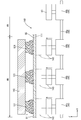
- the driver mounting apparatus 140 is used to mount a plurality of drivers 121 on the liquid crystal panel 111, as shown in FIGS.
- the liquid crystal panel 111 processed by the driver mounting apparatus 140 has a specification with a larger screen size or a higher resolution than the above-described first embodiment, and for this reason, a plurality of drivers 121 are mounted. Yes.
- the liquid crystal panel 111 processed by the driver mounting apparatus 140 has the number of drivers 121 mounted, the arrangement of the drivers 121 (arrangement pitch), and the size of the driver 121 viewed in the plane (long side dimensions, short side dimensions). There are multiple types with different specifications.
- the driver mounting apparatus 140 has the same number (four in this embodiment) of movable substrate heating units as the maximum number of drivers 121 mounted on the liquid crystal panel 111.
- a slide support part 44 is provided for supporting the plurality of movable substrate heating parts 143 in a slidable form. Thereby, it is possible to freely change the number of movable substrate heating units 143 used in mounting the driver 121 and the arrangement in the X-axis direction.
- the movable substrate heating unit 143 can individually heat and press the portion of the glass substrate GS of the array substrate 111b where the driver 121 is mounted.
- the movable substrate heating unit 143 is larger in size in plan view than the maximum size that can be assumed in the driver 121 mounted on the liquid crystal panel 111.
- the slide support portion 44 extends linearly along the X-axis direction (along the plate surface of the glass substrate GS of the array substrate 111b and the arrangement direction of the plurality of drivers 121), and the rail portion 44a.
- an LM guide registered trademark
- a rack and pinion (not shown) is provided to allow the slider 44b to slide. ing.
- the rail portion 44a extends across a mounting area MA where the driver 121 is mounted and a standby area (non-mounting area) WA that is out of the mounting area MA in the X-axis direction.
- the number of sliders 44b is the same as that of the movable substrate heating unit 143 (four in this embodiment), and each slider 44b is slid along the rail unit 44a so that it can freely move between the mounting area MA and the standby area WA. It is possible to go back and forth.
- the movable substrate heating unit 143 is individually assembled to the slider 44b so as to be movable up and down along the Z-axis direction.
- the fixed driver support part 142 is arranged in the mounting area MA and has a size that spans the plurality of drivers 121 in the X-axis direction, and supports the mounted drivers 121 collectively. Is possible. Note that the size (formation range) in the X-axis direction of the fixed driver support portion 142 is further larger than the maximum value of the assumed installation range of the driver 121 mounted on the liquid crystal panel 111.
- the driver mounting apparatus 140 configured as described above, it is possible to suitably process a plurality of types of liquid crystal panels 111 having different numbers of drivers 121 mounted. Specifically, as shown in FIG. 13, in the case of processing the liquid crystal panel 111 having the specification in which the four drivers 121 are mounted in the final crimping step, as shown in FIG. While all the four drivers 121 are collectively supported from the front side, all the four sliders 44b waiting in the standby area WA are slid so as to reach the mounting area MA, and each movable element assembled to each slider 44b is slid. The position of each slider 44b is adjusted so that the expression board heating unit 143 is arranged so as to overlap each driver 121 in plan view.
- each movable substrate heating unit 143 is raised along the Z-axis direction so as to approach the glass substrate GS, and the portion of the glass substrate GS on which the driver 121 is placed is individually added. By pressing and heating, the four drivers 121 can be mounted together.
- FIG. 15 When processing the liquid crystal panels 111 having different numbers and arrangements (arrangement pitches) of the drivers 121, specifically, the liquid crystal panels 111 on which the three drivers 121 are mounted (see FIG. 15), FIG. As shown, three of the four sliders 44b that have been waiting in the standby area WA are slid so as to reach the mounting area MA, and one slider 44b is in standby in the standby area WA.
- Each movable substrate heating unit 143 assembled to the three sliders 44b disposed in the mounting area MA is in a state where all the three drivers 121 are collectively supported from the front side by the fixed driver support unit 142.
- the positions of the three sliders 44b are adjusted so that the driver 121 overlaps the driver 121 in plan view.
- each movable substrate heating unit 143 is raised along the Z-axis direction so as to approach the glass substrate GS, and portions of the glass substrate GS on which the driver 121 is placed are individually set. By pressing and heating, the three drivers 121 can be mounted together.
- the number and arrangement of the movable substrate heating portions 143 used for mounting can be freely and easily changed.
- 111 is suitable for manufacturing.
- the number, arrangement, and size of the driver 121 can be appropriately changed. In this case, the number and arrangement of the movable substrate heating unit 143 used for mounting are changed accordingly. do it. Further, when the size of the driver 121 is changed, the movable substrate heating unit 143 having a different size from the above can be replaced.
- a plurality of movable substrate heating units 143 are provided, but a plurality of movable substrate heating units 143 can be slid in a direction along the plate surface of the glass substrate GS.
- a slide support portion 44 for supporting in a particular shape. In this way, for example, when the number and arrangement of the drivers 121 mounted on the glass substrate GS is changed, the slide support 44 supports the number of drivers 121 on the glass substrate GS and the arrangement. Further, by sliding the plurality of movable substrate heating units 143 in the direction along the plate surface of the glass substrate GS, it is possible to appropriately pressurize and heat the portion of the glass substrate GS where the driver 121 is mounted.
- FIG. 3 A third embodiment of the present invention will be described with reference to FIG.
- movement, and effect as above-mentioned Embodiment 1 is abbreviate
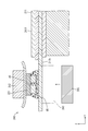
- the driver mounting apparatus 240 includes a cushioning material 45 interposed between the fixed driver support portion 242 and the driver 221 as shown in FIG.
- the buffer material 45 is formed by forming a resin material such as polytetrafluoroethylene (such as Teflon (registered trademark)), polyimide, or aramid into a sheet shape. Since the buffer material 45 can receive and buffer the pressure applied to the driver 221 from the movable substrate heating unit 243 through the glass substrate GS, the driver 221 can be protected. And since this buffer material 45 is the arrangement
- the polarizing plate 211f is altered by heat. It is difficult for problems to occur.
- the shock absorber 45 interposed between the fixed driver support portion 242 and the driver 221 is provided.
- the pressure applied to the driver 221 as the movable substrate heating unit 243 moves so as to approach the fixed driver support unit 242 can be buffered by the buffer material 45,
- the driver 221 can be protected. Since the cushioning material 45 is interposed between the fixed driver support portion 242 and the driver 221, it is difficult to increase the temperature, so that even when the cushioning material 45 comes into contact with another member, It is difficult to cause problems such as deterioration.
- FIG. 4 A fourth embodiment of the present invention will be described with reference to FIG.
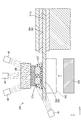
- a driver mounting apparatus 340 including an ultraviolet irradiation unit 46 is shown.
- movement, and effect as above-mentioned Embodiment 1 is abbreviate
- the driver mounting apparatus 340 includes an ultraviolet irradiation unit 46 that can irradiate ultraviolet rays as shown in FIG.
- the anisotropic conductive film 327 for fixing the driver 321 is replaced with the thermosetting resin 27b (see FIG. 7) described in the first embodiment.
- the structure includes an ultraviolet curable resin (photocurable resin) 27c that is cured by ultraviolet rays.
- the ultraviolet curable resin 27c is in a liquid state having fluidity before being irradiated with ultraviolet rays, the ultraviolet curable resin 27c has a property of being cured into a solid state upon being irradiated with ultraviolet rays.
- the ultraviolet irradiation unit 46 is configured to irradiate ultraviolet rays (curing light) having a wavelength that promotes the curing of the ultraviolet curable resin 27c.
- Three ultraviolet irradiation units 46 are arranged on the front side with respect to the fixed driver support unit 342 in the Z-axis direction, that is, on the side opposite to the glass substrate GS of the array substrate 311b, and on the back side with respect to the glass substrate GS, One is arranged on the opposite side to the fixed driver support portion 342.
- the three ultraviolet irradiation units 46 arranged on the front side with respect to the fixed driver support unit 342 are arranged at positions spaced apart from each other in the Y-axis direction.
- the fixed driver support part 342 arranged in the form of being interposed between the ultraviolet irradiation part 46 and the glass substrate GS (anisotropic conductive film 327) in the Z-axis direction is a movable substrate heating part 343.
- High mechanical strength and high thermal conductivity are not required as in the case of, for example, it is made of a substantially transparent (translucent) material such as quartz glass or borosilicate glass (Pyrex (registered trademark)). ing.
- the ultraviolet rays irradiated from the respective ultraviolet irradiation units 46 arranged on the front side with respect to the fixed driver support portion 342 pass through the fixed driver support portion 342, and thereby the front side with respect to the anisotropic conductive film 327. It comes to be irradiated from.
- the amount of ultraviolet light applied to the anisotropic conductive film 327 from the three ultraviolet irradiation units 46 arranged on the front side with respect to the fixed driver support unit 342 was arranged on the back side with respect to the glass substrate GS described below.
- the three ultraviolet irradiation units 46 arranged on the front side with respect to the fixed driver support unit 342 have anisotropic conductive films. It can be said that this is the main configuration (main curing light irradiation part) for curing 327.
- One ultraviolet irradiation unit 46 disposed on the back side with respect to the glass substrate GS is disposed on the outer side with respect to the driver mounting portion GSd of the glass substrate GS in the Y-axis direction, that is, on the side opposite to the substrate main part GSm. .
- the ultraviolet rays irradiated from one ultraviolet irradiation unit 46 arranged on the back side with respect to the glass substrate GS are transmitted through the driver mounting portion GSd of the glass substrate GS, so that the back side (side) )).
- the ultraviolet irradiation unit 46 disposed on the back side of the glass substrate GS hardens the anisotropic conductive film 327 as compared to the three ultraviolet irradiation units 46 disposed on the front side with respect to the fixed driver support unit 342. It can be said that this is an auxiliary configuration (sub-curing light irradiating unit).
- the ultraviolet rays are irradiated from the respective ultraviolet irradiation units 46 toward the anisotropic conductive film 327 while the driver mounting unit GSd of the glass substrate GS is pressurized and heated by the movable substrate heating unit 343. I have to.
- the ultraviolet rays irradiated from the three ultraviolet irradiation units 46 arranged on the front side with respect to the fixed driver support unit 342 pass through the substantially transparent fixed driver support unit 342.
- the anisotropic conductive film 327 is efficiently irradiated.
- the fixed driver support portion 342 is not provided with such a light shielding object.
- the ultraviolet rays irradiated from the portion 46 can be efficiently transmitted, and the anisotropic conductive film 327 can be efficiently cured in a short time by the ultraviolet rays.
- compression-bonding process can be aimed at.
- the anisotropic conductive film 327 is further hardened by heating the anisotropic conductive film 327 through the glass substrate GS by the movable substrate heating unit 343, the tact time related to the main pressure bonding process is further increased. It can be shortened.
- the anisotropic conductive film 327 including the ultraviolet curable resin (photocurable resin) 27 c is interposed between the glass substrate GS and the driver 321, the anisotropic effect is obtained.
- the conductive film 327 includes an ultraviolet irradiation unit (curing light irradiation unit) 46 that radiates curing light, and the fixed driver support unit 342 is made of a light-transmitting material, whereas the ultraviolet irradiation unit. 46 is disposed at least on the side opposite to the glass substrate GS with respect to the fixed driver support portion 342.
- the fixed driver support part 342 does not require high mechanical strength and high thermal conductivity unlike the movable substrate heating part 343, the fixed driver support part 342 can be made of a light-transmitting material.
- the ultraviolet irradiation part 46 is distribute
- the anisotropic conductive film 327 interposed between the glass substrate GS and the driver 321 and including the ultraviolet curable resin 27c is efficiently irradiated.
- the ultraviolet irradiation unit is disposed on the opposite side of the glass substrate GS from the fixed driver support unit 342, if the glass substrate GS is provided with a light shielding material such as a metal wiring, the light is cured by the light shielding material. Compared to light shielding, the irradiation efficiency of the curing light to the anisotropic conductive film 327 becomes higher. As a result, the anisotropic conductive film 327 can be cured in a shorter time, and the tact time for mounting the driver 321 can be shortened.
- the hardening of the anisotropic conductive film 327 is promoted by heating the anisotropic conductive film 327 through the glass substrate GS by the movable substrate heating unit 343, the tact time related to the mounting of the driver 321 is further increased. It can be shortened.
- Embodiment 5 of the present invention will be described with reference to FIG.
- a driver mounting device 440 configured to supply heat to the driver 421 from the fixed driver support portion 442 is shown.
- movement, and effect as above-mentioned Embodiment 1 is abbreviate
- the fixed driver support portion 442 is entirely made of a metal material in order to ensure sufficiently high thermal conductivity, and a heater is used as a heating means inside thereof. Etc. are provided. That is, the driver mounting apparatus 440 is configured to supply heat for thermosetting the anisotropic conductive film 427 from both the fixed driver support portion 442 and the movable substrate heating portion 443. The heat generated from the fixed driver support portion 442 is transmitted to the driver 421 in direct contact with the fixed driver support portion 442 and then transmitted to the anisotropic conductive film 427.
- the fixed driver support unit 442 applies heat to the anisotropic conductive film 427 via the driver 421 from the movable substrate heating unit 443 to the anisotropic conductive film 427 via the glass substrate GS of the array substrate 411b. It is configured to be relatively less than the amount of heat applied. That is, even if the fixed driver support unit 442 supplies heat, the amount of heat supplied from the movable substrate heating unit 443 is dominant. In this way, since the anisotropic conductive film 427 can be thermoset in a shorter time, the tact time related to the main press bonding step can be further shortened.
- the fixed driver support portion 442 and the movable substrate heating portion 443 include the terminal portions 425 and 426 on the driver 421 side and the terminals on the driver mounting portion GSd side.
- Heat is applied so that the temperature at the connection interface with the parts 423 and 424 is 90 ° C. to 200 ° C., and the temperature at the contact surface between the movable substrate heating part 443 and the driver mounting part GSd is 70 ° C. to 150 ° C. Supply.
- FIG. 6 A sixth embodiment of the present invention will be described with reference to FIG.
- movement, and effect as above-mentioned Embodiment 1 is abbreviate
- the flexible substrate (mounting component) 513 is attached to the end of the array substrate 511b forming the liquid crystal panel 511 as shown in FIG. 20 (see FIG. 4). Is electrically connected to the external connection terminal portion 522 disposed in the gap via the conductive particles 527a included in the anisotropic conductive film 527.
- the flexible substrate 513 is provided with a flexible substrate side terminal portion 13a connected to the external connection terminal portion 522 at an end portion on the liquid crystal panel 511 side of the film-like base material. Similar to the external connection terminal portion 522, a large number of the flexible substrate side terminal portions 13a are arranged in a line along the X-axis direction with a predetermined interval.
- a flexible substrate mounting apparatus 47 shown in FIG. 20 is used.
- the flexible substrate mounting apparatus 47 supports the substrate holding portion 541 that holds the substrate main portion GSm in the glass substrate GS that forms the array substrate 511b, and supports the flexible substrate 513 from the opposite side of the glass substrate GS, in the Z-axis direction (glass substrate).
- the fixed flexible substrate support 48 fixed in position with respect to the overlapping direction of the GS and the flexible substrate 513 and the fixed flexible substrate support 48 (fixed mounting component support) 48 opposite to the glass substrate GS.
- a movable substrate heating unit 543 capable of heating the glass substrate GS while applying pressure by being moved so as to approach the fixed flexible substrate support 48 in the Z-axis direction.
- the movable substrate heating unit 543 can pressurize and heat the flexible substrate mounting unit (component mounting unit) GSb on which the flexible substrate 513 is mounted in the glass substrate GS.
- the specific configurations of the substrate holding unit 541 and the movable substrate heating unit 543 constituting the flexible substrate mounting apparatus 47 are the same as those described in the first embodiment.
- the fixed flexible board support 48 is the same as the fixed driver support 42 (see FIGS. 7 and 8) described in the first embodiment except that the support object is the flexible board 513. It is made up of.
- the flexible substrate mounting step includes an anisotropic conductive film mounting step of attaching an anisotropic conductive film 527 to the flexible substrate mounting part GSb of the glass substrate GS constituting the array substrate 511b, and a flexible substrate 513 on the anisotropic conductive film 527.
- At least a temporary press-bonding step for temporarily press-bonding the flexible substrate 513 and a final press-bonding step for press-bonding the flexible substrate 513 at least. In this main press-bonding step, as shown in FIG.
- a liquid crystal panel 511 is placed on a substrate holding portion 541 provided in the flexible substrate mounting apparatus 47 for the purpose of holding it, and the flexible substrate 513 is moved from the front side. It is supported by a fixed flexible substrate support 48.
- the movable substrate heating unit 543 is raised along the Z-axis direction so as to approach the flexible substrate mounting portion GSb in the glass substrate GS, and is brought into surface contact with the outer plate surface in the flexible substrate mounting portion GSb. Then, heat and pressure are applied from the movable substrate heating unit 543 to the flexible substrate mounting unit GSb.
- the movable substrate heating unit 543 is configured to apply heat and pressure to the flexible substrate mounting unit GSb for a predetermined time in a state where the flexible substrate 513 and the flexible substrate mounting unit GSb are sandwiched between the movable flexible substrate support unit 48 and the flexible substrate mounting unit GSb.
- the conductive substrate 527a included in the anisotropic conductive film 527 is interposed between the flexible substrate side terminal portion 13a on the flexible substrate mounting portion GSb side and the external connection terminal portion 522 on the flexible substrate mounting portion GSb side.
- the thermosetting resin 527b included in the anisotropic conductive film 527 is thermoset, and the flexible substrate 513 is finally pressure-bonded to the flexible substrate mounting portion GSb.
- Embodiment 7 A seventh embodiment of the present invention will be described with reference to FIGS.
- the flexible substrate mounting apparatus 647 used for mounting the flexible substrate 613 on the printed circuit board 28 is shown.
- movement, and effect as above-mentioned Embodiment 6 is abbreviate
- the flexible substrate 613 includes a driver 621 mounted on a film-like base material, and one end portion of the base material is placed on the array substrate 611b of the liquid crystal panel 611, and the other base material is placed.
- a printed circuit board (substrate) 28 are mounted on a printed circuit board (substrate) 28, respectively.
- the flexible substrate 613 is electrically connected to the other end portion of the flexible substrate 613 through the conductive particles 627a included in the anisotropic conductive film 627 with respect to the printed circuit board side terminal portion 29 provided on the printed circuit board 28.
- a board side terminal portion 613a is provided.
- a large number of flexible substrate side terminal portions 613a and printed circuit board side terminal portions 29 are arranged in a line along the X axis direction with a predetermined interval.
- the flexible substrates 613 are arranged and connected in such a manner that four of the flexible substrates 613 are intermittently arranged with respect to the end portion along the long side direction in the array substrate 611b forming the liquid crystal panel 611.
- the liquid crystal panel 611 according to this embodiment has a specification with a larger screen size or a higher resolution than the above-described first to sixth embodiments. For this reason, the number of mounting flexible substrates 613 is reduced. Is more than one.
- the flexible board mounting apparatus 647 includes a board holding section 641 that holds the main board portion 28m of the printed board 28, a fixed flexible board support section 648 that supports the flexible board 613 from the side opposite to the printed board 28, and a fixed flexible board.
- a movable substrate heating unit 643 capable of heating the printed circuit board 28 while applying pressure to the substrate support unit 648 so as to move closer to the Z-axis direction.
- the specific configurations of the substrate holding unit 641, the fixed flexible substrate support unit 648, and the movable substrate heating unit 643 forming the flexible substrate mounting apparatus 647 are the same as those described in the first and sixth embodiments.
- This flexible substrate mounting step includes an anisotropic conductive film mounting step of attaching an anisotropic conductive film 627 to the flexible substrate mounting portion 28b on which the flexible substrate 613 is mounted in the printed circuit board 28, and an anisotropic conductive film 627 on the anisotropic conductive film 627. It includes at least a temporary pressure-bonding step for temporarily pressing the flexible substrate 613 and a final pressure-bonding step for pressure-bonding the flexible substrate 613. In this final press-bonding step, as shown in FIG.
- the printed circuit board 28 is placed on the substrate holding portion 641 provided in the flexible substrate mounting apparatus 647 to hold the same, and the flexible substrate 613 is moved from the front side. It is supported by a fixed flexible substrate support 648.
- the movable substrate heating unit 643 is raised along the Z-axis direction so as to approach the flexible substrate mounting portion 28b in the printed circuit board 28, and is in surface contact with the outer plate surface in the flexible substrate mounting portion 28b. Then, heat and pressure are applied from the movable substrate heating unit 643 to the flexible substrate mounting unit 28b.
- the movable substrate heating unit 643 applies heat and pressure to the flexible substrate mounting unit 28b for a predetermined time while the flexible substrate 613 and the flexible substrate mounting unit 28b are sandwiched between the movable substrate heating unit 643 and the fixed flexible substrate support unit 648.
- the conductive substrate 627a included in the anisotropic conductive film 627 is interposed between the flexible substrate side terminal portion 613a on the flexible substrate mounting portion 28b side and the printed circuit board side terminal portion 29 on the flexible substrate mounting portion 28b side.
- the thermosetting resin 627b included in the anisotropic conductive film 627 is thermally cured, and the flexible substrate 613 is finally bonded to the flexible substrate mounting portion 28b.
- FIG. 8 An eighth embodiment of the present invention will be described with reference to FIG.
- the flexible substrate mounting apparatus 747 is used to mount a plurality of flexible substrates 713 on a liquid crystal panel 711 as shown in FIG.
- the liquid crystal panel 711 processed by the flexible substrate mounting apparatus 747 has specifications such as the number of the flexible substrates 713 mounted, the arrangement (arrangement pitch) of the flexible substrates 713, and the size (width dimension) viewed in the plane of the flexible substrate 713.
- FIG. 23 illustrates a liquid crystal panel 711 having the same configuration as that described in the seventh embodiment.
- the flexible substrate mounting apparatus 747 is provided with the same number (four in this embodiment) of movable substrate heating units 743 as the maximum number of flexible substrates 713 mounted on the liquid crystal panel 711.
- a slide support portion 744 that supports the plurality of movable substrate heating portions 743 in a slidable form is provided.
- the configurations of the movable substrate heating unit 743 and the slide support unit 744 are the same as those described in the second embodiment.
- a plurality of types of liquid crystal panels 711 having different numbers of mounted flexible substrates 713 and the like can be suitably processed. This is as described in Form 2.
- a ninth embodiment of the present invention will be described with reference to FIG.
- a driver mounting device 49 for mounting the driver 821 on the flexible substrate 813 is shown.
- the driver mounting apparatus 49 mounts the driver 821 on the film-like base material (substrate) 13b constituting the flexible substrate 813 via the anisotropic conductive film 847. It is used for this purpose.
- the driver mounting device 49 supports a substrate holding portion (not shown) with respect to the base material main part of the base material 13b of the flexible substrate 813 and the driver 821 from the side opposite to the base material 13b.
- Movable base material heating capable of heating while pressing the base material 13b by being moved so as to approach the fixed driver board support portion 842 and the fixed driver board support portion 842 in the Z-axis direction.
- Part (movable substrate heating part) 50 Part
- the movable substrate heating unit 50 is configured so that the movable substrate heating unit 43 (see FIGS. 7 and 8) described in the first embodiment is used except that the heating target is the substrate 13b of the flexible substrate 813. Reference) and the same configuration.
- the present invention is not limited to the embodiments described with reference to the above description and drawings.
- the following embodiments are also included in the technical scope of the present invention.
- (1) As a modification of the above-described first to fifth embodiments, it is possible to perform the driver mounting process in a posture in which the liquid crystal panel is turned upside down in the main pressure bonding step.
- the driver since the driver is mounted on the back surface of the array substrate, the fixed driver support portion is arranged on the back side of the array substrate, that is, on the same side as the substrate holding portion, and the movable substrate heating portion is disposed on the array substrate. It may be arranged on the front side, that is, on the side opposite to the substrate holding part.
- the fixed flexible substrate support portion may be disposed on the back side of the array substrate, that is, on the same side as the substrate holding portion, and the movable substrate heating portion may be disposed on the front side of the array substrate, that is, on the side opposite to the substrate holding portion.
- the fixed flexible board supporting part may be arranged on the back side of the printed board, that is, the same side as the board holding part, and the movable board heating part may be arranged on the front side of the printed board, that is, on the side opposite to the board holding part.
- the fixed driver support portion has a size that spans a plurality of drivers in the X-axis direction and is configured to collectively support the mounted drivers.
- the driver support portion may be divided for each driver.
- the number of installations of the fixed driver support unit can be made to coincide with the number of installations of the movable substrate heating unit.
- the number of installation of the fixed driver support portion may not be the same as the number of installation of the driver.
- the above description regarding the modified example of the fixed driver support portion can be similarly applied to the fixed flexible substrate support portion described in the eighth embodiment.
- the specific number and arrangement of the ultraviolet irradiation units described in the fourth embodiment can be changed as appropriate. Even in such a case, the amount of ultraviolet irradiation from the ultraviolet irradiation unit arranged on the opposite side of the glass substrate with respect to the fixed driver support unit is larger than the amount of ultraviolet irradiation from the ultraviolet irradiation unit arranged on the opposite side. Although it is preferable to set so as to be, it is not always necessary.
- the driver mounting apparatus including the ultraviolet irradiation unit that irradiates ultraviolet rays is shown.
- the anisotropic conductive film includes a visible light curable resin that is cured by visible light.
- the driver mounting device may be provided with a visible light irradiation unit that emits visible light having a wavelength for curing the visible light curable resin.
- an anisotropic conductive film containing an ultraviolet curable resin is used as in the fourth embodiment, and ultraviolet light for curing the anisotropic conductive film. It is also possible to use an irradiation unit.
- the driver having a longitudinal shape is exemplified as the mounting component.
- a driver having a square shape when seen in a plan view can be used as the mounting component.
- a manufacturing apparatus for mounting a driver or a flexible substrate on an array substrate included in a transmissive liquid crystal display device including a backlight device that is an external light source, and a manufacturing method using the same are illustrated.
- the present invention is also applicable to a manufacturing apparatus for mounting a driver or a flexible substrate on an array substrate provided in a reflective liquid crystal display device that performs display using external light, and a manufacturing method using the same.
- a TFT is used as a switching element of a liquid crystal display device.
- a driver or a flexible substrate is provided on an array substrate provided in a liquid crystal display device using a switching element other than TFT (for example, a thin film diode (TFD)).
- TFT thin film diode
- the present invention can also be applied to a manufacturing apparatus for mounting a substrate and a manufacturing method using the same, and besides a liquid crystal display device for color display, a driver or a flexible substrate is included in an array substrate provided in a liquid crystal display device for monochrome display. It is applicable also to the manufacturing apparatus which mounts, and the manufacturing method using the same.
- a manufacturing apparatus for mounting a driver or a flexible substrate on an array substrate provided in a liquid crystal display device using a liquid crystal panel as a display panel and a manufacturing method using the same are exemplified.
- the present invention is also applicable to a manufacturing apparatus for mounting a driver or a flexible substrate on an array substrate provided in a display device using a display panel (such as a PDP or an organic EL panel) and a manufacturing method using the same.
- Substrate holder, 42, 142, 242, 342, 442, 842 Fixed driver support Part (fixed mounting component support part), 43, 143, 243, 343, 443, 543, 643, 743 ... movable substrate heating part, 44, 44 ... Slide support part, 45 ... Buffer material, 46 ... Ultraviolet irradiation part (curing light irradiation part), 47, 647, 747 ... Flexible substrate mounting apparatus (manufacturing apparatus), 48, 648 ... Fixed flexible substrate support part (fixed) Type mounting component support part), 50 ... movable base material heating part (movable board heating part), 513, 613, 713 ... flexible board (mounting part), 813 ... flexible board (mounting board), GS ... glass board ( Board), GSb ... flexible board mounting part (component mounting part), GSd ... driver mounting part (component mounting part), GSm ... main part of board
Landscapes
- Engineering & Computer Science (AREA)
- Manufacturing & Machinery (AREA)
- Microelectronics & Electronic Packaging (AREA)
- Liquid Crystal (AREA)
Abstract
アレイ基板(実装基板)11bのドライバ実装装置(製造装置)40は、ガラス基板(基板)GS上に実装されるドライバ(実装部品)21を該ガラス基板GSとは反対側から支持し、ガラス基板GSとドライバ21の重なり方向について位置固定された固定式ドライバ支持部(固定式実装部品支持部)42と、ガラス基板GSに対して固定式ドライバ支持部42と反対側に配され、固定式ドライバ支持部42に対して重なり方向に接近するよう可動されることでガラス基板GSを加圧しつつ加熱することが可能な可動式基板加熱部43と、を備える。
Description
本発明は、実装基板の製造装置、及び実装基板の製造方法に関する。
携帯電話、スマートフォン、ノートパソコンなどの携帯型の電子機器には、液晶パネルなどの表示パネルを備えた表示装置が用いられている。このような表示装置は、画像を表示する表示部を有する表示パネルと、信号供給源から供給される入力信号を処理して生成した出力信号を表示部に供給することで表示パネルを駆動する半導体チップとを備えている。上記のように一般的に中小型に分類される表示装置においては、半導体チップの実装方法として、半導体チップを表示パネルのうち表示部外の領域に直接実装する、COG(Chip On Glass)実装技術を用いるのが好ましい。なお、この種の表示装置の製造装置の一例として下記特許文献1に記載されたものが知られている。
(発明が解決しようとする課題)
上記した特許文献1には、液晶パネルと、液晶パネルに実装されるTCPとを挟み込むようにして加圧する一対の熱圧着ヘッドを備えた熱圧着実装装置が記載されている。この熱圧着実装装置によれば、液晶パネル及びTCPをそれぞれの熱膨張条件に応じて別個に温度制御しながら加熱することで、液晶パネルに対するTCPの位置合わせを容易にすると共に、TCPにおけるファインパターン接続をし得るようにしている。
上記した特許文献1には、液晶パネルと、液晶パネルに実装されるTCPとを挟み込むようにして加圧する一対の熱圧着ヘッドを備えた熱圧着実装装置が記載されている。この熱圧着実装装置によれば、液晶パネル及びTCPをそれぞれの熱膨張条件に応じて別個に温度制御しながら加熱することで、液晶パネルに対するTCPの位置合わせを容易にすると共に、TCPにおけるファインパターン接続をし得るようにしている。
しかしながら、特許文献1に記載された熱圧着実装装置では、一対の熱圧着ヘッドのそれぞれに加熱のためのパルスヒータなどを設ける必要があるのに加えて、一対の熱圧着ヘッドをそれぞれ昇降させるための昇降機構も必要となるため、構造が複雑化して熱圧着実装装置全体が大型化しがちであるとともに熱圧着実装装置のコスト自体が高くなるという問題がある。そうかといって、従前のように、TCP側にのみ熱圧着ヘッドを設け、液晶パネルの基板側は固定的な基板受け部によって基板を受けるようにすると、TCP及び液晶パネルが薄型化した場合に、実装時に付与される熱に起因して生じるTCPの伸縮量と液晶パネルの伸縮量との差に起因して反りが生じ易くなる、といった問題が生じていた。
本発明は上記のような事情に基づいて完成されたものであって、反りの発生を抑制することを目的とする。
(課題を解決するための手段)
本発明の実装基板の製造装置は、基板上に実装される実装部品を該基板とは反対側から支持し、前記基板と前記実装部品の重なり方向について位置固定された固定式実装部品支持部と、前記基板に対して前記固定式実装部品支持部と反対側に配され、前記固定式実装部品支持部に対して前記重なり方向に接近するよう可動されることで前記基板を加圧しつつ加熱することが可能な可動式基板加熱部と、を備える。
本発明の実装基板の製造装置は、基板上に実装される実装部品を該基板とは反対側から支持し、前記基板と前記実装部品の重なり方向について位置固定された固定式実装部品支持部と、前記基板に対して前記固定式実装部品支持部と反対側に配され、前記固定式実装部品支持部に対して前記重なり方向に接近するよう可動されることで前記基板を加圧しつつ加熱することが可能な可動式基板加熱部と、を備える。
このような構成では、基板と実装部品の重なり方向について位置固定された固定式実装部品支持部によって実装部品を基板とは反対側から支持し、その固定式実装部品支持部に対して可動式基板加熱部を重なり方向に接近するよう可動させることで、基板を加圧しつつ加熱することができ、それにより実装部品を基板に実装することができる。ここで、一般的には、実装部品と基板との比較において、実装部品はシリコン等からなり熱伝導率が相対的に高く、基板はガラス等からなり熱伝導率が相対的に低くなっているので、上記したように重なり方向について位置固定された固定式実装部品支持部によって実装部品を支持しつつ、可動式基板加熱部により基板を加熱する構成とすることで、熱伝導率が相対的に低い基板と、熱伝導率が相対的に高い実装部品との間に生じ得る熱伸縮量の差が緩和される。これにより、基板及び実装部品を薄型化した場合でも実装部品の実装に伴って生じ得る反りを抑制することができる。また、可動式基板加熱部が固定式実装部品支持部に対して接近するよう可動されることで基板を加圧する構成とされているので、従来のように一対の熱圧着ヘッドをそれぞれ昇降させる構成に比べて当該製造装置の構造が簡素化及び小型化されるとともに低コスト化を図ることができる。
本発明の実装基板の製造装置の実施態様として、次の構成が好ましい。
(1)前記固定式実装部品支持部は、前記実装部品を加熱することが可能とされているのに対し、前記可動式基板加熱部は、前記基板に付与する熱量が、前記固定式実装部品支持部から前記実装部品に付与される熱量よりも多くなるよう構成されている。このようにすれば、可動式基板加熱部から基板に付与される熱量が、固定式実装部品支持部から実装部品に付与される熱量よりも多くなっているので、熱伝導率が相対的に低い基板と、熱伝導率が相対的に高い実装部品との間に生じ得る熱伸縮量の差を十分に緩和した上で、実装部品の実装に係るタクトタイムを短縮させることができる。
(1)前記固定式実装部品支持部は、前記実装部品を加熱することが可能とされているのに対し、前記可動式基板加熱部は、前記基板に付与する熱量が、前記固定式実装部品支持部から前記実装部品に付与される熱量よりも多くなるよう構成されている。このようにすれば、可動式基板加熱部から基板に付与される熱量が、固定式実装部品支持部から実装部品に付与される熱量よりも多くなっているので、熱伝導率が相対的に低い基板と、熱伝導率が相対的に高い実装部品との間に生じ得る熱伸縮量の差を十分に緩和した上で、実装部品の実装に係るタクトタイムを短縮させることができる。
(2)前記可動式基板加熱部は、複数備えられているのに対し、複数の前記可動式基板加熱部を前記基板の板面に沿う方向にスライド可能な形で支持するスライド支持部を備えている。このようにすれば、例えば、基板に実装される実装部品の数や配置が変更された場合には、基板における実装部品の数や配置に応じて、スライド支持部によって支持された複数の可動式基板加熱部を、基板の板面に沿う方向にスライドさせることで、基板のうち実装部品が実装される部分を適切に加圧及び加熱することができる。
(3)前記固定式実装部品支持部と前記実装部品との間に介在する緩衝材を備える。このようにすれば、固定式実装部品支持部に対して可動式基板加熱部が接近するよう可動されるのに伴って実装部品に付与される圧力を緩衝材によって緩衝することができ、実装部品の保護を図ることができる。緩衝材は、固定式実装部品支持部と実装部品との間に介在しているので、高温化し難くなっており、それにより、緩衝材が他の部材に接触した場合でもその部材を熱により変質させる、といった問題が生じ難いものとされる。
(4)前記基板と前記実装部品との間に光硬化性樹脂を含む異方性導電膜を介在させる場合に、その異方性導電膜に向けて硬化光を照射する硬化光照射部を備えており、前記固定式実装部品支持部は、透光性を有する材料からなるのに対し、前記硬化光照射部は、前記固定式実装部品支持部に対して前記基板とは反対側に少なくとも配されている。まず、固定式実装部品支持部は、可動式基板加熱部のように高い機械強度や高い熱伝導性が必要とされないので、透光性を有する材料により構成することが可能とされている。そして、硬化光照射部は、固定式実装部品支持部に対して基板とは反対側に少なくとも配されているので、硬化光照射部からの硬化光は、透光性を有する材料からなる固定式実装部品支持部を透過することで、基板と実装部品との間に介在し且つ光硬化性樹脂を含む異方性導電膜に向けて効率的に照射される。従って、仮に硬化光照射部を基板に対して固定式実装部品支持部とは反対側に配置した場合、基板に金属配線などの遮光物が設けられているとその遮光物によって硬化光が遮光されるのに比べると、異方性導電膜に対する硬化光の照射効率がより高いものとなる。これにより、異方性導電膜をより短時間で硬化させることができ、実装部品の実装に係るタクトタイムを短縮させることができる。また、可動式基板加熱部によって基板を介して異方性導電膜を加熱することで異方性導電膜の硬化が促進されるので、実装部品の実装に係るタクトタイムをより短縮させることができる。
(5)前記可動式基板加熱部は、前記基板のうち前記実装部品が実装される部品実装部を選択的に加圧及び加熱する構成とされており、前記基板に対して前記可動式基板加熱部と同じ側に配されるとともに、前記基板のうち前記部品実装部を除いた基板主要部を保持する基板保持部を備える。このようにすれば、基板保持部により基板の基板主要部を保持することで、部品実装部を含めた基板全体の配置を固定化することができるので、基板のうち実装部品が実装される部品実装部を可動式基板加熱部によってより安定的に加圧することができる。これにより、可動式基板加熱部から基板の部品実装部に付与される加圧力によりムラが生じ難くなるので、実装不良がより生じ難いものとされる。
次に、上記課題を解決するために、本発明の実装基板の製造方法は、基板上に実装部品を仮圧着する仮圧着工程と、前記基板上に仮圧着された前記実装部品を、前記基板と前記実装部品の重なり方向について位置固定された固定式実装部品支持部によって前記基板とは反対側から支持した状態で、前記基板に対して前記固定式実装部品支持部と反対側に配された可動式基板加熱部を、前記固定式実装部品支持部に対して前記重なり方向に接近するよう可動させるとともに前記基板を加圧しつつ加熱することで、前記実装部品を前記基板上に本圧着する本圧着工程と、を備える。
仮圧着工程を経て基板上に仮圧着された実装部品は、本圧着工程において、基板と実装部品の重なり方向について位置固定された固定式実装部品支持部により基板とは反対側から支持される。その状態で、固定式実装部品支持部に対して重なり方向に接近するよう可動される可動式基板加熱部によって基板が加圧されつつ加熱されることで、実装部品が基板上に本圧着される。ここで、一般的には、実装部品と基板との比較において、実装部品はシリコン等からなり熱伝導率が相対的に高く、基板はガラス等からなり熱伝導率が相対的に低くなっているので、上記したように重なり方向について位置固定された固定式実装部品支持部によって実装部品を支持しつつ、可動式基板加熱部により基板を加熱する構成とすることで、熱伝導率が相対的に低い基板と、熱伝導率が相対的に高い実装部品との間に生じ得る熱伸縮量の差が緩和される。これにより、基板及び実装部品を薄型化した場合でも実装部品の実装に伴って生じ得る反りを抑制することができる。また、本圧着工程では、可動式基板加熱部が固定式実装部品支持部に対して接近するよう可動されることで基板を加圧する構成の製造装置を用いているので、従来のように一対の熱圧着ヘッドをそれぞれ昇降させる構成の製造装置を用いた場合に比べて当該製造装置の構造が簡素化及び小型化されるとともに低コスト化を図ることができる。
(発明の効果)
本発明によれば、反りの発生を抑制することができる。
本発明によれば、反りの発生を抑制することができる。
<実施形態1>
本発明の実施形態1を図1から図12によって説明する。本実施形態では、液晶表示装置10を構成する液晶パネル(表示パネル)11の製造方法、及びその製造に用いられるドライバ実装装置(製造装置)40について例示する。なお、各図面の一部にはX軸、Y軸及びZ軸を示しており、各軸方向が各図面で示した方向となるように描かれている。また、上下方向については、図2及び図3を基準とし、且つ同図上側を表側とするとともに同図下側を裏側とする。
本発明の実施形態1を図1から図12によって説明する。本実施形態では、液晶表示装置10を構成する液晶パネル(表示パネル)11の製造方法、及びその製造に用いられるドライバ実装装置(製造装置)40について例示する。なお、各図面の一部にはX軸、Y軸及びZ軸を示しており、各軸方向が各図面で示した方向となるように描かれている。また、上下方向については、図2及び図3を基準とし、且つ同図上側を表側とするとともに同図下側を裏側とする。
液晶表示装置10は、図1及び図2に示すように、液晶パネル11と、液晶パネル11に実装されて液晶パネル11を駆動するドライバ(実装部品)21と、ドライバ21に対して各種入力信号を外部から供給する制御回路基板(外部の信号供給源)12と、液晶パネル11と外部の制御回路基板12とを電気的に接続するフレキシブル基板(外部接続部品)13と、液晶パネル11に光を供給する外部光源であるバックライト装置(照明装置)14と、を備える。また、液晶表示装置10は、相互に組み付けた液晶パネル11及びバックライト装置14を収容・保持するための表裏一対の外装部材15,16をも備えており、このうち表側の外装部材15には、液晶パネル11に表示された画像を外部から視認させるための開口部15aが形成されている。本実施形態に係る液晶表示装置10は、携帯型情報端末(電子ブックやPDAなどを含む)、携帯電話(スマートフォンなどを含む)、ノートパソコン(タブレット型ノートパソコンなどを含む)、デジタルフォトフレーム、携帯型ゲーム機、電子インクペーパなどの各種電子機器(図示せず)に用いられるものである。このため、液晶表示装置10を構成する液晶パネル11の画面サイズは、数インチ~10数インチ程度とされ、一般的には小型または中小型に分類される大きさとされている。
先にバックライト装置14について簡単に説明する。バックライト装置14は、図2に示すように、表側(液晶パネル11側)に向けて開口した略箱形をなすシャーシ14aと、シャーシ14a内に配された図示しない光源(例えば冷陰極管、LED、有機ELなど)と、シャーシ14aの開口部を覆う形で配される図示しない光学部材と、を備える。光学部材は、光源から発せられる光を面状に変換するなどの機能を有するものである。
次に、液晶パネル11について説明する。液晶パネル11は、図1に示すように、全体として縦長な方形状(矩形状)をなしており、その長辺方向における一方の端部側(図1に示す上側)に片寄った位置に画像を表示可能な表示領域(アクティブエリア)AAが配されるとともに、長辺方向における他方の端部側(図1に示す下側)に片寄った位置にドライバ21及びフレキシブル基板13がそれぞれ取り付けられている。この液晶パネル11において表示領域AA外の領域が、画像が表示されない非表示領域(ノンアクティブエリア)NAAとされ、この非表示領域NAAの一部がドライバ21及びフレキシブル基板13の実装領域となっている。液晶パネル11における短辺方向が各図面のX軸方向と一致し、長辺方向が各図面のY軸方向と一致している。なお、図1では、CF基板11aよりも一回り小さな枠状の一点鎖線が表示領域AAの外形を表しており、当該一点鎖線よりも外側の領域が非表示領域NAAとなっている。
液晶パネル11は、図3に示すように、一対の透明な(透光性に優れた)基板11a,11bと、両基板11a,11b間に介在し、電界印加に伴って光学特性が変化する物質である液晶分子を含む液晶層11cと、を備え、両基板11a,11bが液晶層11cの厚さ分のセルギャップを維持した状態で図示しないシール剤によって貼り合わせられている。両基板11a,11bは、それぞれ無アルカリガラスや石英ガラスなどからなるガラス基板(基板)GSを備えており、それぞれのガラス基板GS上に既知のフォトリソグラフィ法などによって複数の膜が積層された構成とされる。両基板11a,11bのうち表側(正面側)がCF基板(対向基板)11aとされ、裏側(背面側)がアレイ基板(実装基板、素子基板、アクティブマトリクス基板)11bとされる。このうち、CF基板11aは、図1及び図2に示すように、短辺寸法がアレイ基板11bと概ね同等であるものの、長辺寸法がアレイ基板11bよりも小さなものとされるとともに、アレイ基板11bに対して長辺方向についての一方(図1に示す上側)の端部を揃えた状態で貼り合わせられている。従って、アレイ基板11bのうち長辺方向についての他方(図1に示す下側)の端部は、所定範囲にわたってCF基板11aが重なり合うことがなく、表裏両板面が外部に露出した状態とされており、ここに後述するドライバ21及びフレキシブル基板13の実装領域が確保されている。なお、両基板11a,11bの内面側には、液晶層11cに含まれる液晶分子を配向させるための配向膜11d,11eがそれぞれ形成されている。また、両基板11a,11bの外面側には、それぞれ偏光板11f,11gが貼り付けられている。
続いて、アレイ基板11b及びCF基板11aにおける表示領域AA内に存在する構成について簡単に説明する。アレイ基板11bの内面側(液晶層11c側、CF基板11aとの対向面側)には、図3に示すように、スイッチング素子であるTFT(Thin Film Transistor)17及び画素電極18が多数個ずつマトリクス状に並んで設けられるとともに、これらTFT17及び画素電極18の周りには、格子状をなすゲート配線及びソース配線(共に図示を省略する)が取り囲むようにして配設されている。言い換えると、格子状をなすゲート配線及びソース配線の交差部に、TFT17及び画素電極18が行列状に並列配置されている。ゲート配線とソース配線とがそれぞれTFT17のゲート電極とソース電極とに接続され、画素電極18がTFT17のドレイン電極に接続されている。また、画素電極18は、平面に視て縦長の方形状(矩形状)をなすとともに、ITO(Indium Tin Oxide)或いはZnO(Zinc Oxide)といった透明電極材料からなる。なお、アレイ基板11bには、ゲート配線に並行するとともに画素電極18を横切る容量配線(図示せず)を設けることも可能である。
一方、CF基板11aには、図3に示すように、R(赤色),G(緑色),B(青色)等の各着色部が、アレイ基板11b側の各画素電極18と平面に視て重畳するよう多数個マトリクス状に並列して配置されたカラーフィルタ11hが設けられている。カラーフィルタ11hを構成する各着色部間には、混色を防ぐための略格子状の遮光層(ブラックマトリクス)11iが形成されている。遮光層11iは、上記したゲート配線及びソース配線と平面に視て重畳する配置とされる。カラーフィルタ11h及び遮光層11iの表面には、アレイ基板11b側の画素電極18と対向するベタ状の対向電極11jが設けられている。なお、当該液晶パネル11においては、R(赤色),G(緑色),B(青色)の3色の着色部及びそれらと対向する3つの画素電極18の組によって表示単位である1つの表示画素が構成されている。表示画素は、Rの着色部を有する赤色画素と、Gの着色部を有する緑色画素と、Bの着色部を有する青色画素とからなる。これら各色の画素は、液晶パネル11の板面において行方向(X軸方向)に沿って繰り返し並べて配されることで、画素群を構成しており、この画素群が列方向(Y軸方向)に沿って多数並んで配されている。
次に、液晶パネル11に接続される部材について説明する。制御回路基板12は、図1及び図2に示すように、バックライト装置14におけるシャーシ14aの裏面(液晶パネル11側とは反対側の外面)にネジなどにより取り付けられている。この制御回路基板12は、紙フェノールないしはガラスエポキシ樹脂製の基板上に、ドライバ21に各種入力信号を供給するための電子部品が実装されるとともに、図示しない所定のパターンの配線(導電路)が配索形成されている。この制御回路基板12には、フレキシブル基板13の一方の端部(一端側)が図示しないACF(Anisotropic Conductive Film)を介して電気的に且つ機械的に接続されている。
フレキシブル基板(FPC基板)13は、図2に示すように、絶縁性及び可撓性を有する合成樹脂材料(例えばポリイミド系樹脂等)からなる基材を備え、その基材上に多数本の配線パターン(図示せず)を有しており、長さ方向についての一方の端部が既述した通りシャーシ14aの裏面側に配された制御回路基板12に接続されるのに対し、他方の端部(他端側)が液晶パネル11におけるアレイ基板11bに接続されているため、液晶表示装置10内では断面形状が略U型となるよう折り返し状に屈曲されている。フレキシブル基板13における長さ方向についての両端部においては、配線パターンが外部に露出して端子部(図示せず)を構成しており、これらの端子部がそれぞれ制御回路基板12及び液晶パネル11に対して電気的に接続されている。これにより、制御回路基板12側から供給される入力信号を液晶パネル11側に伝送することが可能とされている。
ドライバ21は、図1に示すように、内部に駆動回路を有するLSIチップからなるものとされ、信号供給源である制御回路基板12から供給される信号に基づいて作動することで、信号供給源である制御回路基板12から供給される入力信号を処理して出力信号を生成し、その出力信号を液晶パネル11の表示領域AAへ向けて出力するものとされる。ドライバ21を構成するLSIチップは、シリコンを高い純度で含んだシリコンウェハ上に配線や素子が形成されてなるものである。このドライバ21は、平面に視て横長の方形状をなす、つまり液晶パネル11の短辺に沿って長手状をなしている。ドライバ21は、液晶パネル11におけるアレイ基板11bの非表示領域NAAに対して直接実装、つまりCOG(Chip On Glass)実装されている。なお、ドライバ21の長辺方向(長手方向)がX軸方向(液晶パネル11の短辺方向)と一致し、同短辺方向(長手方向と直交する方向)がY軸方向(液晶パネル11の長辺方向)と一致している。
次に、アレイ基板11bの非表示領域NAAに対する、フレキシブル基板13及びドライバ21の接続構造について説明する。アレイ基板11bの非表示領域NAAのうちCF基板11aとは重畳しない非重畳部分には、図1に示すように、ドライバ21及びフレキシブル基板13の端部がそれぞれ取り付けられており、フレキシブル基板13の端部がアレイ基板11bにおける短辺方向に沿った端部に配されるのに対して、ドライバ21がアレイ基板11bにおいてフレキシブル基板13よりも表示領域AA側に位置して配されている。言い換えると、ドライバ21は、非表示領域NAAにおいて、表示領域AAとフレキシブル基板13との間に挟まれた位置に配されているのに対し、フレキシブル基板13は、その端部(液晶パネル11に対する取付部位)がドライバ21に対して表示領域AA側とは反対側(アレイ基板11bの端側)に配されている。フレキシブル基板13は、その端部がアレイ基板11bの短辺側の端部における中央部分に取り付けられており、その取り付けられた端部がアレイ基板11bの短辺側の端部(短辺方向、X軸方向)に沿って延在している。フレキシブル基板13におけるアレイ基板11bに対して取り付けられた端部の寸法は、アレイ基板11bの長辺寸法よりも小さくなっている。一方、ドライバ21は、その長辺方向をアレイ基板11bの短辺方向(X軸方向)と一致させた姿勢で非表示領域NAAにおけるアレイ基板11bの短辺方向についての中央部分に実装されている。
上記したアレイ基板11bにおけるフレキシブル基板13の実装領域には、図4に示すように、フレキシブル基板13側から入力信号の供給を受ける外部接続端子部22が形成されている。その一方、アレイ基板11bにおけるドライバ21の実装領域には、ドライバ21への入力信号の供給を図るためのパネル側入力端子部(基板側入力端子部)23と、ドライバ21からの出力信号の供給を受けるパネル側出力端子部(基板側出力端子部)24とが設けられている。また、外部接続端子部22とパネル側入力端子部23とは、非表示領域NAAのうち、フレキシブル基板13の実装領域とドライバ21の実装領域との間を横切る形で配索形成された中継配線(図示せず)によって電気的に接続されている。これに対して、ドライバ21には、パネル側入力端子部23に電気的に接続されるドライバ側入力端子部(実装部品側入力端子部)25と、パネル側出力端子部24に電気的に接続されるドライバ側出力端子部(実装部品側出力端子部)26とが設けられている。なお、図4では、フレキシブル基板13及びドライバ21を二点鎖線により図示している。また、図4では、一点鎖線が表示領域AAの外形を表しており、当該一点鎖線よりも外側の領域が非表示領域NAAとなっている。
パネル側入力端子部23及びパネル側出力端子部24は、図5に示すように、ゲート配線またはソース配線と同じ金属材料からなる薄膜の表面が、画素電極18と同じITO或いはZnOといった透明電極材料によって覆われてなる。従って、パネル側入力端子部23及びパネル側出力端子部24は、液晶パネル11(アレイ基板11b)の製造工程においてゲート配線またはソース配線や画素電極18をパターニングする際に既知のフォトリソグラフィ法によりこれらと同時にアレイ基板11b上にパターニングされている。パネル側入力端子部23及びパネル側出力端子部24上には、異方性導電膜(ACF:Anisotropic Conductive Film)27が配されており、この異方性導電膜27に含まれる導電性粒子27aを介してドライバ21のドライバ側入力端子部25がパネル側入力端子部23に対して、ドライバ側出力端子部26がパネル側出力端子部24に対してそれぞれ電気的に接続されている。異方性導電膜27は、金属材料からなる多数の導電性粒子27aと、多数の導電性粒子27aが分散配合された熱硬化性樹脂27bとからなるものとされている。この異方性導電膜27を介した端子部23~26間の接続は、後に詳しく説明するドライバ実装装置40を用いてドライバ21をアレイ基板11bに実装することで行われるものとされる。なお、図示は省略するが、外部接続端子部22についても上記したパネル側入力端子部23及びパネル側出力端子部24と同様の断面構造を有しており、異方性導電膜を介してフレキシブル基板13の端子部に対して電気的に接続されている。
パネル側入力端子部23及びパネル側出力端子部24は、図4及び図5に示すように、アレイ基板11bのうちドライバ21と平面に視て重畳する位置、つまりドライバ21の実装領域に配されている。パネル側入力端子部23とパネル側出力端子部24とは、間に所定の間隔を空けつつY軸方向(ドライバ21と表示領域AA(フレキシブル基板13)との並び方向)に沿って並んで配されている。このうち、パネル側入力端子部23は、アレイ基板11bにおけるドライバ21の実装領域のうち、フレキシブル基板13側(表示領域AA側とは反対側)に配されているのに対し、パネル側出力端子部24は、表示領域AA側(フレキシブル基板13側とは反対側)に配されている。パネル側入力端子部23及びパネル側出力端子部24は、図6に示すように、X軸方向、つまりドライバ21の長辺方向(長手方向)に沿って多数個ずつがそれぞれ所定の間隔を空けて直線的に並んで配置されている。なお、図6には、各入力端子部23,25の断面構成を代表して例示したが、各出力端子部24,26の断面構成もこれと同様である。
ドライバ側入力端子部25及びドライバ側出力端子部26は、図5に示すように、金などの導電性に優れた金属材料からなるとともにドライバ21の底面(アレイ基板11bとの対向面)から突出するバンプ状(突起状)をなしている。ドライバ側入力端子部25及びドライバ側出力端子部26は、ドライバ21内に有される処理回路にそれぞれ接続されており、ドライバ側入力端子部25から入力された入力信号を処理回路にて処理した後、ドライバ側出力端子部26へと出力することが可能とされる。ドライバ側入力端子部25及びドライバ側出力端子部26は、図6に示すように、パネル側入力端子部23及びパネル側出力端子部24と同様にX軸方向、つまりドライバ21の長辺方向に沿って多数個ずつがそれぞれ所定の間隔を空けて直線的に並んで配置されている。
ところで、近年では、液晶パネル11及び液晶表示装置10を薄型化することが求められており、それに伴ってドライバ21及びドライバ21が実装されるアレイ基板11bを構成するガラス基板GSに関してもそれぞれ薄型化することが求められている。具体的には、ドライバ21の厚みは、従前では、0.2mm~0.3mmの範囲程度とされていたのが、近年では、0.12mm~0.18mmの範囲程度にまで薄型化するのが求められるとともに、アレイ基板11bを構成するガラス基板GSの厚みは、従前では、0.2mm~0.7mmの範囲程度とされていたのが、近年では、0.1mm~0.15mmの範囲程度にまで薄型化するのが求められている。つまり、ガラス基板GSの厚みは、従前では、ドライバ21の厚みよりも大きかったものの、近年では、ドライバ21の厚みよりも小さくすることが求められている。このようにドライバ21及びアレイ基板11bを構成するガラス基板GSの薄型化が進行すると、次の問題が生じることが懸念される。すなわち、ドライバ21の実装に際しては、アレイ基板11bを構成するガラス基板GS上に異方性導電膜27を介してドライバ21を載せた状態で、ドライバ実装装置40によってドライバ21及びガラス基板GSを加圧しつつ異方性導電膜27に含まれる熱硬化性樹脂27bを熱硬化させている。このとき、ドライバ実装装置40から異方性導電膜27に付与される熱は、ドライバ21やガラス基板GSを介して伝達されるのであるが、この熱によってドライバ21及びガラス基板GSは、一旦熱膨張した後に熱収縮することになる。このときのドライバ21の熱伸縮量と、ガラス基板GSの熱伸縮量と、に差が生じ、その差に起因して生じる応力がドライバ21及びガラス基板GSの機械的強度を上回ると、ドライバ21及びガラス基板GSに反りが生じることになる。ここで、ドライバ21及びガラス基板GSは、薄型化に伴ってその機械的強度が低下する傾向にあるため、上記した熱伸縮量の差に起因する反りが、ドライバ21及びガラス基板GSの薄型化の進行に伴ってより発生し易くなっていたのである。
そこで、本実施形態では、アレイ基板11bにドライバ21を実装する際に用いられるドライバ実装装置40を次のような構成としている。すなわち、ドライバ実装装置40は、図7及び図8に示すように、アレイ基板11bを構成するガラス基板GSにおける基板主要部GSmを保持する基板保持部41と、ドライバ21をアレイ基板11bを構成するガラス基板GSとは反対側から支持する固定式ドライバ支持部(固定式実装部品支持部)42と、アレイ基板11bを構成するガラス基板GSに対して固定式ドライバ支持部42と反対側に配されてガラス基板GSのうちドライバ21が実装される部分であるドライバ実装部(部品実装部)GSdを加圧及び加熱する可動式基板加熱部43と、を備えている。このうち、固定式ドライバ支持部42は、Z軸方向、つまりガラス基板GSとドライバ21との重なり方向について位置固定されているのに対し、可動式基板加熱部43は、固定式ドライバ支持部42に対して上記Z軸方向(重なり方向)に接近するよう可動されることで、固定式ドライバ支持部42との間で挟み込んだガラス基板GS及びドライバ21を加圧及び加熱することが可能とされている。なお、図7及び図8では、加圧前の状態の可動式基板加熱部43を実線で、加圧する途中でドライバ実装部GSdに接触した状態の可動式基板加熱部43を二点鎖線で、それぞれ図示している。
このような構成のドライバ実装装置40を用いれば、図9及び図10に示すように、Z軸方向について位置固定された固定式ドライバ支持部42によってドライバ21がガラス基板GSとは反対側から支持され、その状態で固定式ドライバ支持部42に対して可動式基板加熱部43をZ軸方向に接近するよう可動させることで、ガラス基板GSが加圧されつつ加熱され、それによりドライバ21をガラス基板GSに実装することができる。ここで、ドライバ21とガラス基板GSとの比較において、ドライバ21は、シリコンを高純度で含んだシリコンウェハからなるため、熱伝導率が相対的に高くなっているのに対し、ガラス基板GSは、ガラスからなるため、熱伝導率が相対的に低くなっている。従って、上記したようにZ軸方向について位置固定された固定式ドライバ支持部42によってドライバ21を支持しつつ、可動式基板加熱部43によりガラス基板GSを加熱する構成とすることで、熱伝導率が相対的に高いドライバ21に付与される熱量が相対的に少なくなるのに対し、熱伝導率が相対的に低いガラス基板GSに付与される熱量が相対的に多くなり、もって熱伝導率が相対的に低いガラス基板GSと、熱伝導率が相対的に高いドライバ21との間に生じ得る熱伸縮量の差が緩和される。これにより、ガラス基板GS及びドライバ21を薄型化した場合でもドライバ21の実装に伴って生じ得る反りを抑制することができる。また、可動式基板加熱部43が固定式ドライバ支持部42に対して接近するよう可動されることでガラス基板GSを加圧する構成とされているので、従来のように一対の熱圧着ヘッドをそれぞれ昇降させる構成に比べてドライバ実装装置40の構造が簡素化及び小型化されるとともに低コスト化を図ることができる。以下では、ドライバ実装装置40の各構成部位に関して詳しく説明する。
基板保持部41は、図7及び図8に示すように、アレイ基板11bを構成するガラス基板GSのうちの基板主要部GSmを裏側から支持しつつ真空吸着することで、ガラス基板GSの保持を図ることができるものとされる。この基板保持部41によって保持される基板主要部GSmは、アレイ基板11bを構成するガラス基板GSのうち、ドライバ実装部GSdを除いた大部分(具体的には、アレイ基板11bのうちCF基板11aと重畳する部分)である。基板保持部41は、その平面に視た大きさが、アレイ基板11bを構成するガラス基板GSの基板主要部GSmと概ね同じになるようにされており、それにより基板主要部GSmを概ね全域にわたって保持することが可能とされている。また、基板保持部41は、アレイ基板11bを構成するガラス基板GSを直接真空吸着するのではなく、アレイ基板11bに貼り付けられた偏光板11gを直接真空吸着することで、ガラス基板GSを間接的に保持している。
固定式ドライバ支持部42は、図7及び図8に示すように、アレイ基板11bを構成するガラス基板GS上に実装されるドライバ21に対してZ軸方向について表側、つまりガラス基板GS(可動式基板加熱部43)とは反対側に配され、ガラス基板GSのドライバ実装部GSdとの間にドライバ21を介在させた(挟み込んだ)配置とされている。固定式ドライバ支持部42は、ドライバ21をZ軸方向について表側から支持することで、可動式基板加熱部43によってガラス基板GSのドライバ実装部GSdに付与される加圧力を、ドライバ21を介して受けることができるものとされる。ドライバ21を介して固定式ドライバ支持部42によって受けられるドライバ実装部GSdは、アレイ基板11bを構成するガラス基板GSのうち、基板主要部GSmを除いた一部(具体的には、アレイ基板11bのうちCF基板11aとは非重畳となる部分)である。従って、ドライバ実装部GSdは、平面に視た大きさがドライバ21よりも十分に大きなものとされる。固定式ドライバ支持部42は、その平面に視た大きさが、ドライバ21よりも大きくされており、それによりドライバ21を全域にわたって支持することが可能とされる。固定式ドライバ支持部42は、その平面形状がドライバ21に倣って横長な方形状をなしており、その長辺方向がX軸方向と一致し、短辺方向がY軸方向と一致している。固定式ドライバ支持部42は、機械的強度を十分に確保する観点からは金属製とされるのが好ましい。しかし、固定式ドライバ支持部42の材料は、金属以外にすることも可能であり、例えば石英ガラスや硼珪酸ガラス(パイレックス(登録商標)等)といった透光性を有する材料を用いることも可能である。固定式ドライバ支持部42は、その支持面42aがドライバ21における外側の面21aに面接触する形でドライバ21を受けることが可能とされる。
可動式基板加熱部43は、図7及び図8に示すように、アレイ基板11bを構成するガラス基板GSのうちのドライバ実装部GSdに対してZ軸方向について裏側、つまり固定式ドライバ支持部42とは反対側に配され、固定式ドライバ支持部42との間にガラス基板GSのドライバ実装部GSd及びドライバ21を介在させた(挟み込んだ)配置とされている。可動式基板加熱部43は、十分に高い機械的強度及び熱伝導性を担保するために全体が金属材料からなるものとされていて、その内部に加熱手段としてヒータなどが備えられている。その上で、可動式基板加熱部43は、Z軸方向(ガラス基板GSとドライバ21との重なり方向、ガラス基板GSの板面の法線方向)に沿って昇降可能となるよう、図示しない昇降装置によって支持されており、それにより固定式ドライバ支持部42及びガラス基板GSに対してZ軸方向に沿って接近または離間するよう相対変位可能とされている。可動式基板加熱部43は、固定式ドライバ支持部42との間に挟み込んだガラス基板GSのドライバ実装部GSd及びドライバ21を所定の圧力でもって加圧するとともに、ガラス基板GSのドライバ実装部GSdを加熱することが可能とされている。可動式基板加熱部43からガラス基板GSのドライバ実装部GSd及びドライバ21に付与される加圧力によってドライバ21側の端子部25,26と、アレイ基板11b側の端子部23,24との間が異方性導電膜27に含まれる導電性粒子27aを介して電気的に接続されるようになっている。そして、可動式基板加熱部43からガラス基板GSのドライバ実装部GSdに伝達される熱によってドライバ実装部GSdとドライバ21との間に介在する異方性導電膜27を構成する熱硬化性樹脂27bが熱硬化されるようになっている。可動式基板加熱部43は、その平面に視た大きさが、ドライバ21よりも大きくされており、固定式ドライバ支持部42とほぼ同じ大きさとされているので、ドライバ実装部GSdを介して異方性導電膜27に対して効率的に熱及び加圧力を付与することが可能とされている。可動式基板加熱部43は、その平面形状がドライバ21に倣って横長な方形状をなしており、その長辺方向がX軸方向と一致し、短辺方向がY軸方向と一致している。可動式基板加熱部43は、全体が金属製とされることで、熱伝導性及び機械的強度に優れており、それによりガラス基板GSのドライバ実装部GSdに効率的に熱及び加圧力を伝達させることができる。また、可動式基板加熱部43は、金属製とされることで、ドライバ実装部GSdを加圧する加圧面43aが高い加工精度でもって加工されていてその平坦性が十分に高いものとされている。これにより、可動式基板加熱部43は、その加圧面43aがガラス基板GSのドライバ実装部GSdにおける外側の板面に対して面接触した状態で密着するので、熱及び加圧力がより効率的に伝達されるようになっている。
次に、上記のような構成のドライバ実装装置40を用いた液晶パネル(アレイ基板11b)の製造方法について説明する。液晶パネル11の製造方法は、CF基板11a及びアレイ基板11bをなす各ガラス基板GSにおける内側の板面上に既知のフォトリソグラフィ法などによって各種の金属膜や絶縁膜などを積層形成して各種の構造物をそれぞれ形成する構造物形成工程と、CF基板11aをなすガラス基板GSとアレイ基板11bをなすガラス基板GSとを貼り合わせる基板貼り合わせ工程と、各ガラス基板GSの外側の板面に各偏光板11f,11gを貼り付ける偏光板貼付工程と、ドライバ実装装置40を用いてアレイ基板11bを構成するガラス基板GSにおけるドライバ実装部GSdにドライバ21を実装するドライバ実装工程(実装工程)と、を少なくとも含んでいる。このうちのドライバ実装工程は、アレイ基板11bを構成するガラス基板GSにおけるドライバ実装部GSdに異方性導電膜27を取り付ける異方性導電膜取付工程と、異方性導電膜27上にドライバ21を載せて仮圧着する仮圧着工程と、ドライバ21を本圧着する本圧着工程と、を少なくとも含んでいる。また、液晶パネル11の製造方法は、上記した各工程以外にも、フレキシブル基板13を液晶パネル11に実装するフレキシブル基板実装工程なども含んでいる。以下では、アレイ基板11bに係るドライバ実装工程について詳しく説明する。
ドライバ実装工程に含まれる異方性導電膜取付工程では、アレイ基板11bを構成するガラス基板GSにおけるドライバ実装部GSdに異方性導電膜27が取り付けられる。その後、ドライバ実装工程に含まれる仮圧着工程では、ドライバ実装部GSdに取り付けられた異方性導電膜27上にドライバ21が載せられるとともに、その異方性導電膜27に対してドライバ21が仮圧着される。そして、ドライバ実装工程に含まれる本圧着工程では、図7及び図8に示すように、ドライバ実装装置40が用いられており、その基板保持部41の上に、既に偏光板11f,11gが貼り付けられた液晶パネル11が載置される。この状態では、アレイ基板11bをなすガラス基板GSは、基板主要部GSmが基板保持部41により裏側から支持されるのに対し、ドライバ実装部GSd上に仮圧着されたドライバ21は、固定式ドライバ支持部42により表側から支持される。なお、基板主要部GSmは、外側の板面に貼り付けられた偏光板11gが基板保持部41によって真空吸着されることで、強固に保持されている。そして、可動式基板加熱部43がガラス基板GSにおけるドライバ実装部GSdに接近するようZ軸方向に沿って上昇され、ドライバ実装部GSdにおける外側の板面に対して面接触されると、図9及び図10に示すように、ドライバ実装部GSdには可動式基板加熱部43から熱及び加圧力が付与される。可動式基板加熱部43は、固定式ドライバ支持部42との間にドライバ21及びドライバ実装部GSdを挟み込んだ状態で、所定時間の間、熱及び加圧力をドライバ実装部GSdに付与し続ける。これにより、ドライバ21側の端子部25,26と、ドライバ実装部GSd側の端子部23,24との間が異方性導電膜27に含まれる導電性粒子27aを介して電気的に接続されるとともに、異方性導電膜27に含まれる熱硬化性樹脂27bが熱硬化され、もってドライバ21がドライバ実装部GSdに対して本圧着される。この本圧着工程では、可動式基板加熱部43は、ドライバ21側の端子部25,26と、ドライバ実装部GSd側の端子部23,24との接続界面での温度が80℃~150℃となるよう熱を供給するとともに、100N~450Nの荷重をドライバ実装部GSdに付与している。
この本圧着工程では、異方性導電膜27に含まれる熱硬化性樹脂27bを熱硬化させるための熱の供給源が専ら可動式基板加熱部43となっているため、その熱の供給経路は、可動式基板加熱部43からガラス基板GSのドライバ実装部GSdを経て熱硬化性樹脂27bに至る、というものになっている。熱硬化性樹脂27bに達した熱の一部は、非熱源である固定式ドライバ支持部42によって支持されたドライバ21にも伝達されるようになっている。ここで、ガラス基板GSは、熱の供給源である可動式基板加熱部43が直接接触されるものの、ドライバ21に比べると熱伝導率が相対的に低くなっているので、加熱に伴う熱膨張量及びその後の冷却に伴う熱収縮量、つまり熱伸縮量がそれほど大きくならないようになっている。これに対し、ドライバ21は、ガラス基板GSに比べると熱伝導率が相対的に高くなっているものの、熱の供給源である可動式基板加熱部43には直接接触されることがなく、ガラス基板GS及び異方性導電膜27を介して伝熱されているので、その熱伸縮量がガラス基板GSの熱伸縮量と大差ないものとなっている。このように、熱伝導率が相対的に低いガラス基板GSには付与される熱量が相対的に多くされるのに対し、熱伝導率が相対的に高いドライバ21には付与される熱量が相対的に少なくされているので、ガラス基板GSとドライバ21との間に生じ得る熱伸縮量の差が緩和されている。これにより、ガラス基板GS及びドライバ21が薄型化されていても、ドライバ21の実装に伴って生じ得る反りを抑制することができる。
ここで、本実施形態に係るドライバ実装装置40を用いて本圧着工程を行うことで、ガラス基板GSの反りがどの程度抑制されるかに関して知見を得るべく比較実験を行った。この比較実験では、既述した固定式ドライバ支持部42と可動式基板加熱部43とを備えるドライバ実装装置40を実施例とするのに対し、ガラス基板GSを裏側から支持する固定式基板支持部と、ドライバ21を表側から加圧及び加熱する可動式ドライバ加熱部とを備えたドライバ実装装置(図示せず)を比較例としており、これら実施例及び比較例に係る各ドライバ実装装置を用いてそれぞれ本圧着工程を行った各アレイ基板11bのガラス基板GSの反り状態を比較した。ガラス基板GSの反り状態は、ガラス基板GSのドライバ実装部GSdにおける外側の板面とZ軸方向について基準位置との間の距離を測定し、その距離がX軸方向(ドライバ21の長辺方向)の位置に応じてどのように変化するかによって判定することができ、具体的には、上記した距離の最大値及び変化率が大きければ反りが大きく、逆に上記した距離の最大値及び変化率が小さければ反りが小さい、と判定することができる。上記した距離の測定は、ドライバ実装部GSdのうち、ドライバ21と平面に視て重畳する部分をX軸方向について一端から他端に至るまでの範囲で行った。また、上記したZ軸方向についての基準位置は、ガラス基板GSの基板主要部GSmの外側の板面、またはドライバ実装部GSdのうちドライバ21とは非重畳となる部分の外側の板面におけるZ軸方向についての位置である。図11及び図12は、比較実験の実験結果を表す図面である。図11及び図12において、縦軸は、基準位置からドライバ実装部GSdにおける外側の板面までのZ軸方向についての距離(無単位)であり、横軸は、X軸方向についての位置(無単位)である。また、図11及び図12における縦軸及び横軸の縮尺は同一となっている。
比較実験の実験結果について説明する。図11及び図12に示す実験結果によれば、比較例に係るドライバ実装装置を用いた場合の上記距離の最大値D1と、実施例に係るドライバ実装装置40を用いた場合の上記距離の最大値D2と、を比較すると、最大値D2が最大値D1よりも小さくなっており、具体的には約半分程度となっている。このため、上記距離の変化率に関しても、実施例に係るドライバ実装装置40を用いた場合の方が相対的に小さなものとなっている。このことから、実施例に係るドライバ実装装置40を用いた場合の方が、ドライバ実装部GSdに生じた反りが小さく、軽度なものであることが分かる。
以上説明したように本実施形態のアレイ基板(実装基板)11bのドライバ実装装置(製造装置)40は、ガラス基板(基板)GS上に実装されるドライバ(実装部品)21を該ガラス基板GSとは反対側から支持し、ガラス基板GSとドライバ21の重なり方向について位置固定された固定式ドライバ支持部(固定式実装部品支持部)42と、ガラス基板GSに対して固定式ドライバ支持部42と反対側に配され、固定式ドライバ支持部42に対して重なり方向に接近するよう可動されることでガラス基板GSを加圧しつつ加熱することが可能な可動式基板加熱部43と、を備える。
このような構成では、ガラス基板GSとドライバ21の重なり方向について位置固定された固定式ドライバ支持部42によってドライバ21をガラス基板GSとは反対側から支持し、その固定式ドライバ支持部42に対して可動式基板加熱部43を重なり方向に接近するよう可動させることで、ガラス基板GSを加圧しつつ加熱することができ、それによりドライバ21をガラス基板GSに実装することができる。ここで、一般的には、ドライバ21とガラス基板GSとの比較において、ドライバ21はシリコン等からなり熱伝導率が相対的に高く、ガラス基板GSはガラス等からなり熱伝導率が相対的に低くなっているので、上記したように重なり方向について位置固定された固定式ドライバ支持部42によってドライバ21を支持しつつ、可動式基板加熱部43によりガラス基板GSを加熱する構成とすることで、熱伝導率が相対的に低いガラス基板GSと、熱伝導率が相対的に高いドライバ21との間に生じ得る熱伸縮量の差が緩和される。これにより、ガラス基板GS及びドライバ21を薄型化した場合でもドライバ21の実装に伴って生じ得る反りを抑制することができる。また、可動式基板加熱部43が固定式ドライバ支持部42に対して接近するよう可動されることでガラス基板GSを加圧する構成とされているので、従来のように一対の熱圧着ヘッドをそれぞれ昇降させる構成に比べて当該ドライバ実装装置40の構造が簡素化及び小型化されるとともに低コスト化を図ることができる。
また、固定式ドライバ支持部42は、ドライバ21を加熱することが可能とされているのに対し、可動式基板加熱部43は、ガラス基板GSに付与する熱量が、固定式ドライバ支持部42からドライバ21に付与される熱量よりも多くなるよう構成されている。このようにすれば、可動式基板加熱部43からガラス基板GSに付与される熱量が、固定式ドライバ支持部42からドライバ21に付与される熱量よりも多くなっているので、熱伝導率が相対的に低いガラス基板GSと、熱伝導率が相対的に高いドライバ21との間に生じ得る熱伸縮量の差を十分に緩和した上で、ドライバ21の実装に係るタクトタイムを短縮させることができる。
また、可動式基板加熱部43は、ガラス基板GSのうちドライバ21が実装されるドライバ実装部(部品実装部)GSdを選択的に加圧及び加熱する構成とされており、ガラス基板GSに対して可動式基板加熱部43と同じ側に配されるとともに、ガラス基板GSのうちドライバ実装部GSdを除いた基板主要部GSmを保持する基板保持部41を備える。このようにすれば、基板保持部41によりガラス基板GSの基板主要部GSmを保持することで、ドライバ実装部GSdを含めたガラス基板GS全体の配置を固定化することができるので、ガラス基板GSのうちドライバ21が実装されるドライバ実装部GSdを可動式基板加熱部43によってより安定的に加圧することができる。これにより、可動式基板加熱部43からガラス基板GSのドライバ実装部GSdに付与される加圧力によりムラが生じ難くなるので、実装不良がより生じ難いものとされる。
また、本実施形態のアレイ基板11bの製造方法は、ガラス基板GS上にドライバ21を仮圧着する仮圧着工程と、ガラス基板GS上に仮圧着されたドライバ21を、ガラス基板GSとドライバ21の重なり方向について位置固定された固定式ドライバ支持部42によってガラス基板GSとは反対側から支持した状態で、ガラス基板GSに対して固定式ドライバ支持部42と反対側に配された可動式基板加熱部43を、固定式ドライバ支持部42に対して重なり方向に接近するよう可動させるとともにガラス基板GSを加圧しつつ加熱することで、ドライバ21をガラス基板GS上に本圧着する本圧着工程と、を備える。
仮圧着工程を経てガラス基板GS上に仮圧着されたドライバ21は、本圧着工程において、ガラス基板GSとドライバ21の重なり方向について位置固定された固定式ドライバ支持部42によりガラス基板GSとは反対側から支持される。その状態で、固定式ドライバ支持部42に対して重なり方向に接近するよう可動される可動式基板加熱部43によってガラス基板GSが加圧されつつ加熱されることで、ドライバ21がガラス基板GS上に本圧着される。ここで、一般的には、ドライバ21とガラス基板GSとの比較において、ドライバ21はシリコン等からなり熱伝導率が相対的に高く、ガラス基板GSはガラス等からなり熱伝導率が相対的に低くなっているので、上記したように重なり方向について位置固定された固定式ドライバ支持部42によってドライバ21を支持しつつ、可動式基板加熱部43によりガラス基板GSを加熱する構成とすることで、熱伝導率が相対的に低いガラス基板GSと、熱伝導率が相対的に高いドライバ21との間に生じ得る熱伸縮量の差が緩和される。これにより、ガラス基板GS及びドライバ21を薄型化した場合でもドライバ21の実装に伴って生じ得る反りを抑制することができる。また、本圧着工程では、可動式基板加熱部43が固定式ドライバ支持部42に対して接近するよう可動されることでガラス基板GSを加圧する構成のドライバ実装装置40を用いているので、従来のように一対の熱圧着ヘッドをそれぞれ昇降させる構成のドライバ実装装置を用いた場合に比べて当該ドライバ実装装置40の構造が簡素化及び小型化されるとともに低コスト化を図ることができる。
<実施形態2>
本発明の実施形態2を図13から図16によって説明する。この実施形態2では、複数の可動式基板加熱部143をスライド可能な形で備えるドライバ実装装置140を示す。なお、上記した実施形態1と同様の構造、作用及び効果について重複する説明は省略する。
本発明の実施形態2を図13から図16によって説明する。この実施形態2では、複数の可動式基板加熱部143をスライド可能な形で備えるドライバ実装装置140を示す。なお、上記した実施形態1と同様の構造、作用及び効果について重複する説明は省略する。
本実施形態に係るドライバ実装装置140は、図13及び図14に示すように、液晶パネル111にドライバ121を複数実装するのに用いられるものである。ドライバ実装装置140によって処理がなされる液晶パネル111は、上記した実施形態1に比べて画面サイズが大きい仕様、または解像度が高い仕様とされており、そのためにドライバ121の実装数が複数となっている。さらには、ドライバ実装装置140によって処理がなされる液晶パネル111は、ドライバ121の実装数、ドライバ121の配置(配列ピッチ)、ドライバ121の平面に視た大きさ(長辺寸法、短辺寸法)などの仕様が異なる複数種類となっている。これに対してドライバ実装装置140には、図14に示すように、液晶パネル111に実装されるドライバ121の実装想定数の最大値と同数(本実施形態では4つ)の可動式基板加熱部143が備えられているのに加えて、それら複数の可動式基板加熱部143をスライド可能な形で支持するスライド支持部44が備えられている。これにより、ドライバ121の実装に際して使用する可動式基板加熱部143の数及びX軸方向についての配置を自由に変更することが可能とされている。可動式基板加熱部143は、アレイ基板111bのガラス基板GSのうちドライバ121が実装される部分を個別に加熱及び加圧することが可能とされる。また、可動式基板加熱部143は、その平面に視た大きさが、液晶パネル111に実装されるドライバ121において想定され得る最大の大きさよりもさらに大きなものとされる。スライド支持部44は、X軸方向(アレイ基板111bのガラス基板GSの板面に沿い且つ複数のドライバ121の並び方向)に沿って直線的に延在するレール部44aと、レール部44aに対してその延在方向についてスライド可能な形で取り付けられる複数のスライダ44bと、を備えるのに加えて、スライダ44bのスライドを可能とするために図示しないLMガイド(登録商標)またはラックアンドピニオンを備えている。レール部44aは、ドライバ121の実装処理がなされる実装領域MAと、実装領域MAに対してX軸方向について外れた待機領域(非実装領域)WAと、に跨る形で延在している。スライダ44bは、可動式基板加熱部143と同数(本実施形態では4つ)備えられるとともに、それぞれがレール部44aに沿ってスライドされることで、実装領域MAと待機領域WAとの間を自在に行き来することが可能とされる。可動式基板加熱部143は、スライダ44bに対してZ軸方向に沿って昇降可能な形で個別に組み付けられている。一方、固定式ドライバ支持部142は、上記した実装領域MAに配されるとともにX軸方向について複数のドライバ121に跨る大きさを有しており、実装されるドライバ121を一括して支持することが可能とされる。なお、固定式ドライバ支持部142におけるX軸方向についての大きさ(形成範囲)は、液晶パネル111に実装されるドライバ121の設置想定範囲の最大値よりもさらに大きなものとされる。
上記のような構成のドライバ実装装置140によれば、ドライバ121の実装数などが異なる複数種類の液晶パネル111を好適に処理することができる。具体的には、図13に示すように、本圧着工程において4つのドライバ121が実装される仕様の液晶パネル111を処理する場合には、図14に示すように、固定式ドライバ支持部142によって4つのドライバ121を全て一括して表側から支持した状態としつつ、待機領域WAに待機させていた4つのスライダ44bを全て実装領域MAに至るようスライドさせるとともに、各スライダ44bに組み付けられた各可動式基板加熱部143が各ドライバ121と平面に視て重畳する配置となるよう各スライダ44bの位置調整を行う。各スライダ44bの位置調整がなされたら、各可動式基板加熱部143をガラス基板GSに接近するようZ軸方向に沿って上昇させ、ガラス基板GSのうちドライバ121が載せられた部分を個別に加圧及び加熱することで、4つのドライバ121を一括して実装することができる。そして、ドライバ121の実装数及び配置(配列ピッチ)が異なる液晶パネル111、具体的には3つのドライバ121が実装される液晶パネル111(図15を参照)を処理する場合には、図16に示すように、待機領域WAに待機させていた4つのスライダ44bのうちの3つのスライダ44bを実装領域MAに至るようスライドさせ、1つのスライダ44bに関しては待機領域WAに待機させておく。そして、固定式ドライバ支持部142によって3つのドライバ121を全て一括して表側から支持した状態としつつ、実装領域MAに配された3つのスライダ44bに組み付けられた各可動式基板加熱部143が各ドライバ121と平面に視て重畳する配置となるよう3つのスライダ44bの位置調整を行う。3つのスライダ44bの位置調整がなされたら、各可動式基板加熱部143をガラス基板GSに接近するようZ軸方向に沿って上昇させ、ガラス基板GSのうちドライバ121が載せられた部分を個別に加圧及び加熱することで、3つのドライバ121を一括して実装することができる。このように、スライダ44bをレール部44aに沿ってスライドさせることで、実装に使用する可動式基板加熱部143の数及び配置を自由に且つ容易に変更することができるので、多品種の液晶パネル111を製造するのに好適とされる。なお、上記以外にもドライバ121の実装数、配置、及び大きさは適宜に変更することが可能であり、その場合にはそれに応じて実装に用いる可動式基板加熱部143の数及び配置を変更すればよい。また、ドライバ121の大きさが変更された場合、上記とは大きさが異なる可動式基板加熱部143を換装することも可能である。
以上説明したように本実施形態によれば、可動式基板加熱部143は、複数備えられているのに対し、複数の可動式基板加熱部143をガラス基板GSの板面に沿う方向にスライド可能な形で支持するスライド支持部44を備えている。このようにすれば、例えば、ガラス基板GSに実装されるドライバ121の数や配置が変更された場合には、ガラス基板GSにおけるドライバ121の数や配置に応じて、スライド支持部44によって支持された複数の可動式基板加熱部143を、ガラス基板GSの板面に沿う方向にスライドさせることで、ガラス基板GSのうちドライバ121が実装される部分を適切に加圧及び加熱することができる。
<実施形態3>
本発明の実施形態3を図17によって説明する。この実施形態3では、固定式ドライバ支持部242とドライバ221との間に緩衝材45を介在させたドライバ実装装置240を示す。なお、上記した実施形態1と同様の構造、作用及び効果について重複する説明は省略する。
本発明の実施形態3を図17によって説明する。この実施形態3では、固定式ドライバ支持部242とドライバ221との間に緩衝材45を介在させたドライバ実装装置240を示す。なお、上記した実施形態1と同様の構造、作用及び効果について重複する説明は省略する。
本実施形態に係るドライバ実装装置240は、図17に示すように、固定式ドライバ支持部242とドライバ221との間に介在する緩衝材45を備えている。緩衝材45は、例えばポリテトラフルオロエチレン(テフロン(登録商標)など)、ポリイミド、アラミドなどの樹脂材料をシート状に形成してなるものとされる。この緩衝材45により、可動式基板加熱部243からガラス基板GSを介してドライバ221に作用する加圧力を受けて緩衝することができるので、ドライバ221の保護を図ることができる。そして、この緩衝材45は、熱の供給源である可動式基板加熱部243とは非接触となる配置とされているので、高温化し難くなっている。従って、緩衝材45が例えば液晶パネル211のうちアレイ基板211bのガラス基板GSに対して固定式ドライバ支持部242側に配される偏光板211fに接触した場合でも、その偏光板211fが熱によって変質させられる、といった問題が生じ難いものとなっている。
以上説明したように本実施形態によれば、固定式ドライバ支持部242とドライバ221との間に介在する緩衝材45を備える。このようにすれば、固定式ドライバ支持部242に対して可動式基板加熱部243が接近するよう可動されるのに伴ってドライバ221に付与される圧力を緩衝材45によって緩衝することができ、ドライバ221の保護を図ることができる。緩衝材45は、固定式ドライバ支持部242とドライバ221との間に介在しているので、高温化し難くなっており、それにより、緩衝材45が他の部材に接触した場合でもその部材を熱により変質させる、といった問題が生じ難いものとされる。
<実施形態4>
本発明の実施形態4を図18によって説明する。この実施形態4では、紫外線照射部46を備えたドライバ実装装置340を示す。なお、上記した実施形態1と同様の構造、作用及び効果について重複する説明は省略する。
本発明の実施形態4を図18によって説明する。この実施形態4では、紫外線照射部46を備えたドライバ実装装置340を示す。なお、上記した実施形態1と同様の構造、作用及び効果について重複する説明は省略する。
本実施形態に係るドライバ実装装置340は、図18に示すように、紫外線を照射することが可能な紫外線照射部46を備えている。当該ドライバ実装装置340によって処理される液晶パネル311は、ドライバ321を固着する異方性導電膜327が、上記した実施形態1に記載した熱硬化性樹脂27b(図7を参照)に代えて、紫外線によって硬化される紫外線硬化性樹脂(光硬化性樹脂)27cを含む構成とされている。紫外線硬化性樹脂27cは、紫外線の照射を受ける前では流動性を有する液体状態とされるものの、紫外線の照射を受けると硬化して固体状態となる性質を有している。紫外線照射部46は、この紫外線硬化性樹脂27cの硬化を促進させる波長の紫外線(硬化光)を照射する構成とされている。
紫外線照射部46は、Z軸方向について固定式ドライバ支持部342に対して表側、つまりアレイ基板311bのガラス基板GSとは反対側に3つ配されるとともに、ガラス基板GSに対して裏側、つまり固定式ドライバ支持部342とは反対側に1つ配されている。固定式ドライバ支持部342に対して表側に配された3つの紫外線照射部46は、Y軸方向について所定の間隔を空けた位置に配されている。これに対して、Z軸方向について紫外線照射部46とガラス基板GS(異方性導電膜327)との間に介在する形で配される固定式ドライバ支持部342は、可動式基板加熱部343のように高い機械的強度や高い熱伝導性が必要とされないので、例えば石英ガラスや硼珪酸ガラス(パイレックス(登録商標)等)といったほぼ透明な(透光性を有する)材料からなるものとされている。従って、固定式ドライバ支持部342に対して表側に配された各紫外線照射部46から照射された紫外線は、固定式ドライバ支持部342を透過することで、異方性導電膜327に対して表側から照射されるようになっている。固定式ドライバ支持部342に対して表側に配された3つの紫外線照射部46から異方性導電膜327に照射される紫外線の光量は、次述するガラス基板GSに対して裏側に配された紫外線照射部46から照射される紫外線の光量よりも相対的に多くなっていることから、固定式ドライバ支持部342に対して表側に配された3つの紫外線照射部46が、異方性導電膜327を硬化させるための主要な構成(主硬化光照射部)である、と言える。ガラス基板GSに対して裏側に配された1つの紫外線照射部46は、Y軸方向についてガラス基板GSのドライバ実装部GSdに対して外側、つまり基板主要部GSmとは反対側に配されている。ガラス基板GSに対して裏側に配された1つの紫外線照射部46か照射された紫外線は、ガラス基板GSのドライバ実装部GSdを透過することで、異方性導電膜327に対して裏側(側方)から照射されるようになっている。このガラス基板GSに対して裏側に配された紫外線照射部46は、固定式ドライバ支持部342に対して表側に配された3つの紫外線照射部46に比べると、異方性導電膜327を硬化させるための補助的な構成(副硬化光照射部)である、と言える。
そして、本圧着工程では、可動式基板加熱部343によりガラス基板GSのドライバ実装部GSdを加圧及び加熱しつつ、各紫外線照射部46から紫外線を異方性導電膜327に向けて照射するようにしている。4つの紫外線照射部46のうち、固定式ドライバ支持部342に対して表側に配された3つの紫外線照射部46から照射される紫外線は、ほぼ透明な固定式ドライバ支持部342を透過することで、異方性導電膜327に対して効率的に照射される。ここで、固定式ドライバ支持部342は、金属配線などの遮光物が設けられたアレイ基板311bのガラス基板GSに比べると、そのような遮光物が設けられていないので、上記した3つの紫外線照射部46から照射される紫外線を効率的に透過させることができ、もって該紫外線によって異方性導電膜327を短時間で効率的に硬化させることができる。これにより、本圧着工程に係るタクトタイムの短縮化を図ることができる。しかも、可動式基板加熱部343によってガラス基板GSを介して異方性導電膜327を加熱することで異方性導電膜327の硬化がより促進されるので、本圧着工程に係るタクトタイムを一層短縮させることができる。
以上説明したように本実施形態によれば、ガラス基板GSとドライバ321との間に紫外線硬化性樹脂(光硬化性樹脂)27cを含む異方性導電膜327を介在させる場合に、その異方性導電膜327に向けて硬化光を照射する紫外線照射部(硬化光照射部)46を備えており、固定式ドライバ支持部342は、透光性を有する材料からなるのに対し、紫外線照射部46は、固定式ドライバ支持部342に対してガラス基板GSとは反対側に少なくとも配されている。まず、固定式ドライバ支持部342は、可動式基板加熱部343のように高い機械強度や高い熱伝導性が必要とされないので、透光性を有する材料により構成することが可能とされている。そして、紫外線照射部46は、固定式ドライバ支持部342に対してガラス基板GSとは反対側に少なくとも配されているので、紫外線照射部46からの硬化光は、透光性を有する材料からなる固定式ドライバ支持部342を透過することで、ガラス基板GSとドライバ321との間に介在し且つ紫外線硬化性樹脂27cを含む異方性導電膜327に向けて効率的に照射される。従って、仮に紫外線照射部をガラス基板GSに対して固定式ドライバ支持部342とは反対側に配置した場合、ガラス基板GSに金属配線などの遮光物が設けられているとその遮光物によって硬化光が遮光されるのに比べると、異方性導電膜327に対する硬化光の照射効率がより高いものとなる。これにより、異方性導電膜327をより短時間で硬化させることができ、ドライバ321の実装に係るタクトタイムを短縮させることができる。また、可動式基板加熱部343によってガラス基板GSを介して異方性導電膜327を加熱することで異方性導電膜327の硬化が促進されるので、ドライバ321の実装に係るタクトタイムをより短縮させることができる。
<実施形態5>
本発明の実施形態5を図19によって説明する。この実施形態5では、固定式ドライバ支持部442からドライバ421に熱を供給するようにしたドライバ実装装置440を示す。なお、上記した実施形態1と同様の構造、作用及び効果について重複する説明は省略する。
本発明の実施形態5を図19によって説明する。この実施形態5では、固定式ドライバ支持部442からドライバ421に熱を供給するようにしたドライバ実装装置440を示す。なお、上記した実施形態1と同様の構造、作用及び効果について重複する説明は省略する。
本実施形態に係る固定式ドライバ支持部442は、図19に示すように、十分に高い熱伝導性を担保するために全体が金属材料からなるものとされていて、その内部に加熱手段としてヒータなどが備えられている。つまり、このドライバ実装装置440は、固定式ドライバ支持部442と可動式基板加熱部443との双方から異方性導電膜427を熱硬化させるための熱を供給する構成となっている。固定式ドライバ支持部442から発せられた熱は、固定式ドライバ支持部442が直接接触するドライバ421に伝達されてから、異方性導電膜427に伝達されるようになっている。この固定式ドライバ支持部442は、ドライバ421を介して異方性導電膜427に付与する熱量が、可動式基板加熱部443からアレイ基板411bのガラス基板GSを介して異方性導電膜427に付与する熱量よりも相対的に少なくなるよう構成されている。つまり、固定式ドライバ支持部442が熱量を供給する構成であっても、あくまで可動式基板加熱部443から供給される熱量が支配的となっている。このようにすれば、異方性導電膜427をより短時間でもって熱硬化させることができるので、本圧着工程に係るタクトタイムをより短縮させることができる。なお、このドライバ実装装置440を用いて行われる本圧着工程では、固定式ドライバ支持部442及び可動式基板加熱部443は、ドライバ421側の端子部425,426と、ドライバ実装部GSd側の端子部423,424との接続界面での温度が90℃~200℃となるとともに、可動式基板加熱部443とドライバ実装部GSdとの接触面での温度が70℃~150℃となるよう熱を供給している。
<実施形態6>
本発明の実施形態6を図20によって説明する。この実施形態6では、液晶パネル511にフレキシブル基板513を実装するのに用いるフレキシブル基板実装装置47を示す。なお、上記した実施形態1と同様の構造、作用及び効果について重複する説明は省略する。
本発明の実施形態6を図20によって説明する。この実施形態6では、液晶パネル511にフレキシブル基板513を実装するのに用いるフレキシブル基板実装装置47を示す。なお、上記した実施形態1と同様の構造、作用及び効果について重複する説明は省略する。
上記した実施形態1に記載した通り、フレキシブル基板(実装部品)513は、図20に示すように、液晶パネル511をなすアレイ基板511bの端部に取り付けられることで(図4を参照)、そこに配された外部接続端子部522に対して異方性導電膜527に含まれる導電性粒子527aを介して電気的に接続されている。フレキシブル基板513には、フィルム状の基材における液晶パネル511側の端部に、外部接続端子部522に対して接続されるフレキシブル基板側端子部13aが設けられている。フレキシブル基板側端子部13aは、外部接続端子部522と同様に、X軸方向に沿って多数個が所定の間隔を空けて直線的に並ぶ形で配置されている。
上記した構成のフレキシブル基板513を液晶パネル511に実装するフレキシブル基板実装工程では、図20に示すフレキシブル基板実装装置47が用いられている。フレキシブル基板実装装置47は、アレイ基板511bをなすガラス基板GSにおける基板主要部GSmを保持する基板保持部541と、フレキシブル基板513をガラス基板GSとは反対側から支持し、Z軸方向(ガラス基板GSとフレキシブル基板513との重なり方向)について位置固定された固定式フレキシブル基板支持部48と、ガラス基板GSに対して固定式フレキシブル基板支持部(固定式実装部品支持部)48とは反対側に配され、固定式フレキシブル基板支持部48に対してZ軸方向に接近するよう可動されることで、ガラス基板GSを加圧しつつ加熱することが可能な可動式基板加熱部543と、を備える。可動式基板加熱部543は、ガラス基板GSのうちフレキシブル基板513が実装されるフレキシブル基板実装部(部品実装部)GSbを加圧及び加熱することが可能とされる。フレキシブル基板実装装置47をなす基板保持部541及び可動式基板加熱部543の具体的な構成に関しては、上記した実施形態1に記載したものと同様である。また、固定式フレキシブル基板支持部48は、支持対象物がフレキシブル基板513である点を除けば、上記した実施形態1に記載した固定式ドライバ支持部42(図7及び図8を参照)と同様の構成とされる。
次に、液晶パネル511の製造方法に含まれる工程であって、フレキシブル基板513を液晶パネル511に実装するフレキシブル基板実装工程について説明する。フレキシブル基板実装工程は、アレイ基板511bを構成するガラス基板GSにおけるフレキシブル基板実装部GSbに異方性導電膜527を取り付ける異方性導電膜取付工程と、異方性導電膜527上にフレキシブル基板513を載せて仮圧着する仮圧着工程と、フレキシブル基板513を本圧着する本圧着工程と、を少なくとも含んでいる。このうちの本圧着工程では、図20に示すように、フレキシブル基板実装装置47に備えられる基板保持部541の上に液晶パネル511を載置してその保持を図るとともに、フレキシブル基板513を表側から固定式フレキシブル基板支持部48によって支持する。この状態で、可動式基板加熱部543がガラス基板GSにおけるフレキシブル基板実装部GSbに接近するようZ軸方向に沿って上昇され、フレキシブル基板実装部GSbにおける外側の板面に対して面接触されると、フレキシブル基板実装部GSbには可動式基板加熱部543から熱及び加圧力が付与される。可動式基板加熱部543は、固定式フレキシブル基板支持部48との間にフレキシブル基板513及びフレキシブル基板実装部GSbを挟み込んだ状態で、所定時間の間、熱及び加圧力をフレキシブル基板実装部GSbに付与し続ける。これにより、フレキシブル基板実装部GSb側のフレキシブル基板側端子部13aと、フレキシブル基板実装部GSb側の外部接続端子部522との間が異方性導電膜527に含まれる導電性粒子527aを介して電気的に接続されるとともに、異方性導電膜527に含まれる熱硬化性樹脂527bが熱硬化され、もってフレキシブル基板513がフレキシブル基板実装部GSbに対して本圧着される。
<実施形態7>
本発明の実施形態7を図21及び図22によって説明する。この実施形態7では、フレキシブル基板613の構成を変更するとともに、プリント基板28にフレキシブル基板613を実装するのに用いるフレキシブル基板実装装置647を示す。なお、上記した実施形態6と同様の構造、作用及び効果について重複する説明は省略する。
本発明の実施形態7を図21及び図22によって説明する。この実施形態7では、フレキシブル基板613の構成を変更するとともに、プリント基板28にフレキシブル基板613を実装するのに用いるフレキシブル基板実装装置647を示す。なお、上記した実施形態6と同様の構造、作用及び効果について重複する説明は省略する。
フレキシブル基板613は、図21及び図22に示すように、フィルム状の基材にドライバ621が搭載されるとともに、基材における一方の端部が液晶パネル611のアレイ基板611bに、基材における他方の端部がプリント基板(基板)28に、それぞれ実装されている。フレキシブル基板613における他方の端部には、プリント基板28に備えられたプリント基板側端子部29に対して異方性導電膜627に含まれる導電性粒子627aを介して電気的に接続されるフレキシブル基板側端子部613aが設けられている。フレキシブル基板側端子部613a及びプリント基板側端子部29は、X軸方向に沿って多数個ずつが所定の間隔を空けてそれぞれ直線的に並ぶ形で配置されている。また、フレキシブル基板613は、液晶パネル611をなすアレイ基板611bにおける長辺方向に沿った端部に対して4つが間欠的に並んだ形で配置・接続されている。このように、本実施形態に係る液晶パネル611は、上記した実施形態1~6に比べて画面サイズがさらに大きい仕様、または解像度がさらに高い仕様とされており、そのためにフレキシブル基板613の実装数が複数となっている。
上記した構成のフレキシブル基板613をプリント基板28に実装するフレキシブル基板実装工程では、図22に示すフレキシブル基板実装装置647が用いられている。フレキシブル基板実装装置647は、プリント基板28における基板主要部28mを保持する基板保持部641と、フレキシブル基板613をプリント基板28とは反対側から支持する固定式フレキシブル基板支持部648と、固定式フレキシブル基板支持部648に対してZ軸方向に接近するよう可動されることで、プリント基板28を加圧しつつ加熱することが可能な可動式基板加熱部643と、を備える。フレキシブル基板実装装置647をなす基板保持部641、固定式フレキシブル基板支持部648、可動式基板加熱部643の具体的な構成に関しては、上記した実施形態1,6に記載したものと同様である。
次に、プリント基板28にフレキシブル基板613を実装するフレキシブル基板実装工程について説明する。このフレキシブル基板実装工程は、プリント基板28のうちフレキシブル基板613が実装されるフレキシブル基板実装部28bに異方性導電膜627を取り付ける異方性導電膜取付工程と、異方性導電膜627上にフレキシブル基板613を載せて仮圧着する仮圧着工程と、フレキシブル基板613を本圧着する本圧着工程と、を少なくとも含んでいる。このうちの本圧着工程では、図22に示すように、フレキシブル基板実装装置647に備えられる基板保持部641の上にプリント基板28を載置してその保持を図るとともに、フレキシブル基板613を表側から固定式フレキシブル基板支持部648によって支持する。この状態で、可動式基板加熱部643がプリント基板28におけるフレキシブル基板実装部28bに接近するようZ軸方向に沿って上昇され、フレキシブル基板実装部28bにおける外側の板面に対して面接触されると、フレキシブル基板実装部28bには可動式基板加熱部643から熱及び加圧力が付与される。可動式基板加熱部643は、固定式フレキシブル基板支持部648との間にフレキシブル基板613及びフレキシブル基板実装部28bを挟み込んだ状態で、所定時間の間、熱及び加圧力をフレキシブル基板実装部28bに付与し続ける。これにより、フレキシブル基板実装部28b側のフレキシブル基板側端子部613aと、フレキシブル基板実装部28b側のプリント基板側端子部29との間が異方性導電膜627に含まれる導電性粒子627aを介して電気的に接続されるとともに、異方性導電膜627に含まれる熱硬化性樹脂627bが熱硬化され、もってフレキシブル基板613がフレキシブル基板実装部28bに対して本圧着される。
<実施形態8>
本発明の実施形態8を図23によって説明する。この実施形態8では、複数の可動式基板加熱部743をスライド可能な形で備えるフレキシブル基板実装装置747を示す。なお、上記した実施形態2,7と同様の構造、作用及び効果について重複する説明は省略する。
本発明の実施形態8を図23によって説明する。この実施形態8では、複数の可動式基板加熱部743をスライド可能な形で備えるフレキシブル基板実装装置747を示す。なお、上記した実施形態2,7と同様の構造、作用及び効果について重複する説明は省略する。
本実施形態に係るフレキシブル基板実装装置747は、図23に示すように、液晶パネル711にフレキシブル基板713を複数実装するのに用いられるものである。フレキシブル基板実装装置747によって処理がなされる液晶パネル711は、フレキシブル基板713の実装数、フレキシブル基板713の配置(配列ピッチ)、フレキシブル基板713の平面に視た大きさ(幅寸法)などの仕様が異なる複数種類となっている。なお、図23には、上記した実施形態7に記載したものと同じ構成の液晶パネル711が例示されている。これに対してフレキシブル基板実装装置747には、液晶パネル711に実装されるフレキシブル基板713の実装想定数の最大値と同数(本実施形態では4つ)の可動式基板加熱部743が備えられているのに加えて、それら複数の可動式基板加熱部743をスライド可能な形で支持するスライド支持部744が備えられている。これにより、フレキシブル基板713の実装に際して使用する可動式基板加熱部743の数及びX軸方向についての配置を自由に変更することが可能とされている。なお、可動式基板加熱部743及びスライド支持部744の構成に関しては、上記した実施形態2に記載したものと同様である。そして、上記のような構成のフレキシブル基板実装装置747によれば、フレキシブル基板713の実装数などが異なる複数種類の液晶パネル711を好適に処理することができ、その作用及び効果については上記した実施形態2に記載した通りである。
<実施形態9>
本発明の実施形態9を図24によって説明する。この実施形態9では、フレキシブル基板813にドライバ821を実装するためのドライバ実装装置49を示す。なお、上記した実施形態7と同様の構造、作用及び効果について重複する説明は省略する。
本発明の実施形態9を図24によって説明する。この実施形態9では、フレキシブル基板813にドライバ821を実装するためのドライバ実装装置49を示す。なお、上記した実施形態7と同様の構造、作用及び効果について重複する説明は省略する。
本実施形態に係るドライバ実装装置49は、図24に示すように、フレキシブル基板813を構成するフィルム状の基材(基板)13bに対して異方性導電膜847を介してドライバ821を実装するために用いられるものである。ドライバ実装装置49は、フレキシブル基板813の基材13bにおける基材主要部を保持する基板保持部(基材主要部共々図示せず)と、ドライバ821とは基材13bとは反対側から支持する固定式ドライバ基板支持部842と、固定式ドライバ基板支持部842に対してZ軸方向に接近するよう可動されることで、基材13bを加圧しつつ加熱することが可能な可動式基材加熱部(可動式基板加熱部)50と、を備える。ドライバ実装装置49をなす基板保持部及び固定式ドライバ基板支持部842の具体的な構成に関しては、上記した実施形態1に記載したものと同様である。また、可動式基材加熱部50は、加熱対象物がフレキシブル基板813の基材13bである点を除けば、上記した実施形態1に記載した可動式基板加熱部43(図7及び図8を参照)と同様の構成とされる。
<他の実施形態>
本発明は上記記述及び図面によって説明した実施形態に限定されるものではなく、例えば次のような実施形態も本発明の技術的範囲に含まれる。
(1)上記した実施形態1~5の変形例として、本圧着工程において液晶パネルを表裏反転した姿勢でドライバの実装処理を行うようにすることも可能である。その場合、アレイ基板における裏側の面にドライバが実装されることになるので、固定式ドライバ支持部をアレイ基板の裏側、つまり基板保持部と同じ側に配置し、可動式基板加熱部をアレイ基板の表側、つまり基板保持部とは反対側に配置すればよい。
本発明は上記記述及び図面によって説明した実施形態に限定されるものではなく、例えば次のような実施形態も本発明の技術的範囲に含まれる。
(1)上記した実施形態1~5の変形例として、本圧着工程において液晶パネルを表裏反転した姿勢でドライバの実装処理を行うようにすることも可能である。その場合、アレイ基板における裏側の面にドライバが実装されることになるので、固定式ドライバ支持部をアレイ基板の裏側、つまり基板保持部と同じ側に配置し、可動式基板加熱部をアレイ基板の表側、つまり基板保持部とは反対側に配置すればよい。
(2)上記した(1)と同様に、実施形態6,8の変形例として、本圧着工程において液晶パネルを表裏反転した姿勢でフレキシブル基板の実装処理を行うようにすることも可能である。その場合、固定式フレキシブル基板支持部をアレイ基板の裏側、つまり基板保持部と同じ側に配置し、可動式基板加熱部をアレイ基板の表側、つまり基板保持部とは反対側に配置すればよい。
(3)上記した(1),(2)と同様に、実施形態7の変形例として、本圧着工程においてプリント基板を表裏反転した姿勢でフレキシブル基板の実装処理を行うようにすることも可能である。その場合、固定式フレキシブル基板支持部をプリント基板の裏側、つまり基板保持部と同じ側に配置し、可動式基板加熱部をプリント基板の表側、つまり基板保持部とは反対側に配置すればよい。
(4)上記した(1)~(3)と同様に、実施形態9の変形例として、本圧着工程においてフレキシブル基板を表裏反転した姿勢でドライバの実装処理を行うようにすることも可能である。その場合、固定式ドライバ基板支持部をフレキシブル基板の裏側、つまり基板保持部と同じ側に配置し、可動式基材加熱部をフレキシブル基板の表側、つまり基板保持部とは反対側に配置すればよい。
(5)上記した実施形態2では、固定式ドライバ支持部がX軸方向について複数のドライバに跨る大きさとされ、実装されるドライバを一括して支持する構成としたものを示したが、固定式ドライバ支持部が各ドライバ毎に対応して分割された構成であっても構わない。その場合、固定式ドライバ支持部の設置数を、可動式基板加熱部の設置数と一致させることができる。また、固定式ドライバ支持部の設置数がドライバの想定される設置数と一致しない構成であっても構わない。上記した固定式ドライバ支持部の変形例に関する説明は、実施形態8に記載した固定式フレキシブル基板支持部にも同様に適用することが可能である。
(6)上記した実施形態2,8以外にも、可動式基板加熱部の具体的な設置数や大きさなどは適宜に変更することが可能である。
(7)上記した実施形態3に記載した緩衝材の具体的な材料は適宜に変更可能である。
(8)上記した実施形態4に記載した紫外線照射部の具体的な設置数や配置は適宜に変更可能である。その場合でも、固定式ドライバ支持部に対してガラス基板とは反対側に配置した紫外線照射部からの紫外線の照射光量が、その反対側に配置した紫外線照射部からの紫外線の照射光量よりも多くなるよう設定するのが好ましいが、必ずしもそうでなくてもよい。
(9)上記した実施形態4では、紫外線を照射する紫外線照射部を備えたドライバ実装装置を示したが、例えば異方性導電膜が可視光線によって硬化する可視光線硬化性樹脂を含むものであった場合には、その可視光線硬化性樹脂を硬化させる波長の可視光線を照射する可視光線照射部をドライバ実装装置に備えさせるようにすればよい。
(10)上記した実施形態4を除いた各実施形態において、実施形態4と同様に紫外線硬化性樹脂を含んだ異方性導電膜を用いるとともに、その異方性導電膜を硬化させるための紫外線照射部を用いるようにすることも可能である。
(11)上記した実施形態7以外にも、液晶パネルに接続するフレキシブル基板の数や配置は適宜に変更することが可能である。
(12)上記した実施形態7では、ドライバを搭載したフレキシブル基板をプリント基板に実装する際に用いるフレキシブル基板実装装置を示したが、ドライバを搭載したフレキシブル基板を液晶パネルに実装する際には、実施形態6に記載したフレキシブル基板実装装置を用いるようにすればよい。
(13)上記した各実施形態では、実装部品として長手状をなすドライバを例示したが、例えば、平面に視て正方形状をなすドライバを実装部品とすることも可能である。
(14)上記した各実施形態では、外部光源であるバックライト装置を備えた透過型の液晶表示装置に備わるアレイ基板にドライバやフレキシブル基板を実装する製造装置及びそれを用いた製造方法を例示したが、本発明は、外光を利用して表示を行う反射型液晶表示装置に備わるアレイ基板にドライバやフレキシブル基板を実装する製造装置及びそれを用いた製造方法にも適用可能である。
(15)上記した各実施形態では、液晶表示装置のスイッチング素子としてTFTを用いたが、TFT以外のスイッチング素子(例えば薄膜ダイオード(TFD))を用いた液晶表示装置に備わるアレイ基板にドライバやフレキシブル基板を実装する製造装置及びそれを用いた製造方法にも本発明は適用可能であり、さらにはカラー表示する液晶表示装置以外にも、白黒表示する液晶表示装置に備わるアレイ基板にドライバやフレキシブル基板を実装する製造装置及びそれを用いた製造方法にも適用可能である。
(16)上記した各実施形態では、表示パネルとして液晶パネルを用いた液晶表示装置に備わるアレイ基板にドライバやフレキシブル基板を実装する製造装置及びそれを用いた製造方法を例示したが、他の種類の表示パネル(PDPや有機ELパネルなど)を用いた表示装置に備わるアレイ基板にドライバやフレキシブル基板を実装する製造装置及びそれを用いた製造方法にも本発明は適用可能である。
11b,111b,211b,311b,411b,511b,611b…アレイ基板(実装基板)、13b…基材(基板)、21,121,221,421,621,821…ドライバ(実装部品)、27,327,427,527,627…異方性導電膜、27c…紫外線硬化性樹脂(光硬化性樹脂)、28…プリント基板(基板)、28b…フレキシブル基板実装部(部品実装部)、28m…基板主要部、40,49,140,240,340,440,540…ドライバ実装装置(製造装置)、41,541,641…基板保持部、42,142,242,342,442,842…固定式ドライバ支持部(固定式実装部品支持部)、43,143,243,343,443,543,643,743…可動式基板加熱部、44,744…スライド支持部、45…緩衝材、46…紫外線照射部(硬化光照射部)、47,647,747…フレキシブル基板実装装置(製造装置)、48,648…固定式フレキシブル基板支持部(固定式実装部品支持部)、50…可動式基材加熱部(可動式基板加熱部)、513,613,713…フレキシブル基板(実装部品)、813…フレキシブル基板(実装基板)、GS…ガラス基板(基板)、GSb…フレキシブル基板実装部(部品実装部)、GSd…ドライバ実装部(部品実装部)、GSm…基板主要部
Claims (7)
- 基板上に実装される実装部品を該基板とは反対側から支持し、前記基板と前記実装部品の重なり方向について位置固定された固定式実装部品支持部と、
前記基板に対して前記固定式実装部品支持部と反対側に配され、前記固定式実装部品支持部に対して前記重なり方向に接近するよう可動されることで前記基板を加圧しつつ加熱することが可能な可動式基板加熱部と、を備える実装基板の製造装置。 - 前記固定式実装部品支持部は、前記実装部品を加熱することが可能とされているのに対し、前記可動式基板加熱部は、前記基板に付与する熱量が、前記固定式実装部品支持部から前記実装部品に付与される熱量よりも多くなるよう構成されている請求項1記載の実装基板の製造装置。
- 前記可動式基板加熱部は、複数備えられているのに対し、複数の前記可動式基板加熱部を前記基板の板面に沿う方向にスライド可能な形で支持するスライド支持部を備えている請求項1または請求項2記載の実装基板の製造装置。
- 前記固定式実装部品支持部と前記実装部品との間に介在する緩衝材を備える請求項1から請求項3のいずれか1項に記載の実装基板の製造装置。
- 前記基板と前記実装部品との間に光硬化性樹脂を含む異方性導電膜を介在させる場合に、その異方性導電膜に向けて硬化光を照射する硬化光照射部を備えており、
前記固定式実装部品支持部は、透光性を有する材料からなるのに対し、前記硬化光照射部は、前記固定式実装部品支持部に対して前記基板とは反対側に少なくとも配されている請求項1から請求項4のいずれか1項に記載の実装基板の製造装置。 - 前記可動式基板加熱部は、前記基板のうち前記実装部品が実装される部品実装部を選択的に加圧及び加熱する構成とされており、
前記基板に対して前記可動式基板加熱部と同じ側に配されるとともに、前記基板のうち前記部品実装部を除いた基板主要部を保持する基板保持部を備える請求項1から請求項5のいずれか1項に記載の実装基板の製造装置。 - 基板上に実装部品を仮圧着する仮圧着工程と、
前記基板上に仮圧着された前記実装部品を、前記基板と前記実装部品の重なり方向について位置固定された固定式実装部品支持部によって前記基板とは反対側から支持した状態で、前記基板に対して前記固定式実装部品支持部と反対側に配された可動式基板加熱部を、前記固定式実装部品支持部に対して前記重なり方向に接近するよう可動させるとともに前記基板を加圧しつつ加熱することで、前記実装部品を前記基板上に本圧着する本圧着工程と、を備える実装基板の製造方法。
Applications Claiming Priority (2)
| Application Number | Priority Date | Filing Date | Title |
|---|---|---|---|
| JP2014-013341 | 2014-01-28 | ||
| JP2014013341 | 2014-01-28 |
Publications (1)
| Publication Number | Publication Date |
|---|---|
| WO2015114863A1 true WO2015114863A1 (ja) | 2015-08-06 |
Family
ID=53756463
Family Applications (1)
| Application Number | Title | Priority Date | Filing Date |
|---|---|---|---|
| PCT/JP2014/072432 Ceased WO2015114863A1 (ja) | 2014-01-28 | 2014-08-27 | 実装基板の製造装置、及び実装基板の製造方法 |
Country Status (1)
| Country | Link |
|---|---|
| WO (1) | WO2015114863A1 (ja) |
Cited By (1)
| Publication number | Priority date | Publication date | Assignee | Title |
|---|---|---|---|---|
| WO2017149426A1 (en) * | 2016-02-29 | 2017-09-08 | Thin Film Electronics Asa | Electronic device and method of making the same using surface mount technology and an anisotropic conductive adhesive useful in the method |
Citations (3)
| Publication number | Priority date | Publication date | Assignee | Title |
|---|---|---|---|---|
| JP2000058567A (ja) * | 1998-08-05 | 2000-02-25 | Matsushita Electric Ind Co Ltd | 半導体装置の組立用治具及び組立方法 |
| JP2004045593A (ja) * | 2002-07-10 | 2004-02-12 | Matsushita Electric Ind Co Ltd | 表示パネルの加工方法およびその加工装置 |
| JP2009032845A (ja) * | 2007-07-26 | 2009-02-12 | Sony Chemical & Information Device Corp | 熱圧着装置及び電気部品の実装方法 |
-
2014
- 2014-08-27 WO PCT/JP2014/072432 patent/WO2015114863A1/ja not_active Ceased
Patent Citations (3)
| Publication number | Priority date | Publication date | Assignee | Title |
|---|---|---|---|---|
| JP2000058567A (ja) * | 1998-08-05 | 2000-02-25 | Matsushita Electric Ind Co Ltd | 半導体装置の組立用治具及び組立方法 |
| JP2004045593A (ja) * | 2002-07-10 | 2004-02-12 | Matsushita Electric Ind Co Ltd | 表示パネルの加工方法およびその加工装置 |
| JP2009032845A (ja) * | 2007-07-26 | 2009-02-12 | Sony Chemical & Information Device Corp | 熱圧着装置及び電気部品の実装方法 |
Cited By (2)
| Publication number | Priority date | Publication date | Assignee | Title |
|---|---|---|---|---|
| WO2017149426A1 (en) * | 2016-02-29 | 2017-09-08 | Thin Film Electronics Asa | Electronic device and method of making the same using surface mount technology and an anisotropic conductive adhesive useful in the method |
| CN109076706A (zh) * | 2016-02-29 | 2018-12-21 | 薄膜电子有限公司 | 使用表面安装技术和该方法中有用的各向异性导电胶的电子装置及其制造方法 |
Similar Documents
| Publication | Publication Date | Title |
|---|---|---|
| US8319109B2 (en) | Electro-optical device and electronic apparatus | |
| US9239495B2 (en) | Display device, electronic device including display device, and method for manufacturing display device | |
| JP4367553B2 (ja) | 電気光学装置、および電子機器 | |
| US20180004030A1 (en) | Mounting substrate and display device | |
| WO2016027762A1 (ja) | 実装基板の製造装置、及び実装基板の製造方法 | |
| KR20080031091A (ko) | 표시장치 및 이의 제조 방법 | |
| CN101178490A (zh) | 电光装置的制造方法 | |
| JP2020027190A (ja) | 表示装置 | |
| WO2016088615A1 (ja) | 湾曲型表示パネルの製造方法 | |
| WO2011111420A1 (ja) | 液晶表示装置とその製造方法 | |
| KR20210027579A (ko) | 표시장치 및 이의 제조 방법 | |
| WO2015182496A1 (ja) | 実装基板、実装基板の製造方法、及び実装基板の製造装置 | |
| US10237981B2 (en) | Method of manufacturing mounting substrate and mounting substrate manufacturing apparatus | |
| US10816857B2 (en) | Display device | |
| WO2017038670A1 (ja) | 表示パネルの製造方法及び表示パネル | |
| US11291111B2 (en) | Flexible wiring substrate, electro-optical device, and electronic apparatus | |
| WO2015114863A1 (ja) | 実装基板の製造装置、及び実装基板の製造方法 | |
| US7591651B2 (en) | Substrate with helically curved terminals superimposed and connected to identical terminals on a second substrate | |
| WO2016114206A1 (ja) | 実装基板の製造装置、及び実装基板の製造方法 | |
| WO2016088594A1 (ja) | 実装基板の製造装置、及び実装基板の製造方法 | |
| WO2017006856A1 (ja) | 表示装置及び駆動回路部品の製造方法 | |
| JP2006171601A (ja) | 実装構造体、電気光学装置の製造方法および電気光学装置並びに電子機器 | |
| JP4868035B2 (ja) | 基板接続構造体の製造方法 | |
| WO2015107715A1 (ja) | 実装基板の製造装置、及び実装基板の製造方法 | |
| JP4407406B2 (ja) | 基板接続構造体、電気光学装置および電子機器 |
Legal Events
| Date | Code | Title | Description |
|---|---|---|---|
| 121 | Ep: the epo has been informed by wipo that ep was designated in this application |
Ref document number: 14880519 Country of ref document: EP Kind code of ref document: A1 |
|
| NENP | Non-entry into the national phase |
Ref country code: DE |
|
| NENP | Non-entry into the national phase |
Ref country code: JP |
|
| 122 | Ep: pct application non-entry in european phase |
Ref document number: 14880519 Country of ref document: EP Kind code of ref document: A1 |