WO2015104886A1 - 電力変換装置 - Google Patents
電力変換装置 Download PDFInfo
- Publication number
- WO2015104886A1 WO2015104886A1 PCT/JP2014/078622 JP2014078622W WO2015104886A1 WO 2015104886 A1 WO2015104886 A1 WO 2015104886A1 JP 2014078622 W JP2014078622 W JP 2014078622W WO 2015104886 A1 WO2015104886 A1 WO 2015104886A1
- Authority
- WO
- WIPO (PCT)
- Prior art keywords
- phase
- converter
- diodes
- load
- power
- Prior art date
- Legal status (The legal status is an assumption and is not a legal conclusion. Google has not performed a legal analysis and makes no representation as to the accuracy of the status listed.)
- Ceased
Links
Images




Classifications
-
- H—ELECTRICITY
- H02—GENERATION; CONVERSION OR DISTRIBUTION OF ELECTRIC POWER
- H02M—APPARATUS FOR CONVERSION BETWEEN AC AND AC, BETWEEN AC AND DC, OR BETWEEN DC AND DC, AND FOR USE WITH MAINS OR SIMILAR POWER SUPPLY SYSTEMS; CONVERSION OF DC OR AC INPUT POWER INTO SURGE OUTPUT POWER; CONTROL OR REGULATION THEREOF
- H02M5/00—Conversion of AC power input into AC power output, e.g. for change of voltage, for change of frequency, for change of number of phases
- H02M5/40—Conversion of AC power input into AC power output, e.g. for change of voltage, for change of frequency, for change of number of phases with intermediate conversion into DC
- H02M5/42—Conversion of AC power input into AC power output, e.g. for change of voltage, for change of frequency, for change of number of phases with intermediate conversion into DC by static converters
- H02M5/44—Conversion of AC power input into AC power output, e.g. for change of voltage, for change of frequency, for change of number of phases with intermediate conversion into DC by static converters using discharge tubes or semiconductor devices to convert the intermediate DC into AC
- H02M5/453—Conversion of AC power input into AC power output, e.g. for change of voltage, for change of frequency, for change of number of phases with intermediate conversion into DC by static converters using discharge tubes or semiconductor devices to convert the intermediate DC into AC using devices of a triode or transistor type requiring continuous application of a control signal
- H02M5/458—Conversion of AC power input into AC power output, e.g. for change of voltage, for change of frequency, for change of number of phases with intermediate conversion into DC by static converters using discharge tubes or semiconductor devices to convert the intermediate DC into AC using devices of a triode or transistor type requiring continuous application of a control signal using semiconductor devices only
- H02M5/4585—Conversion of AC power input into AC power output, e.g. for change of voltage, for change of frequency, for change of number of phases with intermediate conversion into DC by static converters using discharge tubes or semiconductor devices to convert the intermediate DC into AC using devices of a triode or transistor type requiring continuous application of a control signal using semiconductor devices only having a rectifier with controlled elements
-
- H—ELECTRICITY
- H02—GENERATION; CONVERSION OR DISTRIBUTION OF ELECTRIC POWER
- H02M—APPARATUS FOR CONVERSION BETWEEN AC AND AC, BETWEEN AC AND DC, OR BETWEEN DC AND DC, AND FOR USE WITH MAINS OR SIMILAR POWER SUPPLY SYSTEMS; CONVERSION OF DC OR AC INPUT POWER INTO SURGE OUTPUT POWER; CONTROL OR REGULATION THEREOF
- H02M1/00—Details of apparatus for conversion
- H02M1/0048—Circuits or arrangements for reducing losses
- H02M1/0054—Transistor switching losses
-
- H—ELECTRICITY
- H02—GENERATION; CONVERSION OR DISTRIBUTION OF ELECTRIC POWER
- H02M—APPARATUS FOR CONVERSION BETWEEN AC AND AC, BETWEEN AC AND DC, OR BETWEEN DC AND DC, AND FOR USE WITH MAINS OR SIMILAR POWER SUPPLY SYSTEMS; CONVERSION OF DC OR AC INPUT POWER INTO SURGE OUTPUT POWER; CONTROL OR REGULATION THEREOF
- H02M7/00—Conversion of AC power input into DC power output; Conversion of DC power input into AC power output
- H02M7/42—Conversion of DC power input into AC power output without possibility of reversal
- H02M7/44—Conversion of DC power input into AC power output without possibility of reversal by static converters
- H02M7/48—Conversion of DC power input into AC power output without possibility of reversal by static converters using discharge tubes with control electrode or semiconductor devices with control electrode
- H02M7/53—Conversion of DC power input into AC power output without possibility of reversal by static converters using discharge tubes with control electrode or semiconductor devices with control electrode using devices of a triode or transistor type requiring continuous application of a control signal
- H02M7/537—Conversion of DC power input into AC power output without possibility of reversal by static converters using discharge tubes with control electrode or semiconductor devices with control electrode using devices of a triode or transistor type requiring continuous application of a control signal using semiconductor devices only, e.g. single switched pulse inverters
- H02M7/539—Conversion of DC power input into AC power output without possibility of reversal by static converters using discharge tubes with control electrode or semiconductor devices with control electrode using devices of a triode or transistor type requiring continuous application of a control signal using semiconductor devices only, e.g. single switched pulse inverters with automatic control of output wave form or frequency
- H02M7/5395—Conversion of DC power input into AC power output without possibility of reversal by static converters using discharge tubes with control electrode or semiconductor devices with control electrode using devices of a triode or transistor type requiring continuous application of a control signal using semiconductor devices only, e.g. single switched pulse inverters with automatic control of output wave form or frequency by pulse-width modulation
-
- Y—GENERAL TAGGING OF NEW TECHNOLOGICAL DEVELOPMENTS; GENERAL TAGGING OF CROSS-SECTIONAL TECHNOLOGIES SPANNING OVER SEVERAL SECTIONS OF THE IPC; TECHNICAL SUBJECTS COVERED BY FORMER USPC CROSS-REFERENCE ART COLLECTIONS [XRACs] AND DIGESTS
- Y02—TECHNOLOGIES OR APPLICATIONS FOR MITIGATION OR ADAPTATION AGAINST CLIMATE CHANGE
- Y02B—CLIMATE CHANGE MITIGATION TECHNOLOGIES RELATED TO BUILDINGS, e.g. HOUSING, HOUSE APPLIANCES OR RELATED END-USER APPLICATIONS
- Y02B70/00—Technologies for an efficient end-user side electric power management and consumption
- Y02B70/10—Technologies improving the efficiency by using switched-mode power supplies [SMPS], i.e. efficient power electronics conversion e.g. power factor correction or reduction of losses in power supplies or efficient standby modes
Definitions
- Embodiment of this invention is related with the power converter device which converts the voltage of AC power supply into DC, and converts the converted DC voltage into AC voltage of a predetermined frequency.
- a boost converter that has a reactor, a diode, and a switching element and boosts and converts the voltage of an AC power source has a large power loss of the switching element and a large power loss of the reactor. If the switching is not performed, the conversion efficiency is improved, but if this is done, the harmonic current cannot be suppressed, the voltage cannot be boosted, and the power source power factor is also reduced.
- An object of an embodiment of the present invention is to provide a power conversion device capable of reducing power loss while enabling suppression of harmonic current, boosting, and reduction of power source power factor.
- the power conversion device includes a converter and a controller.
- the converter boosts and converts DC voltage of the AC power supply.
- the controller generates a PWM signal by pulse width modulation, drives the converter by the PWM signal, and switches the modulation condition of the pulse width modulation according to the load of the power converter.
- a converter 2 is connected to an R phase, an S phase, and a T phase of a commercial three-phase AC power source 1, and a smoothing capacitor 4 is connected to an output terminal of the converter 2.
- the inverter 5 is connected to the smoothing capacitor 4, and the phase windings Lu, Lv, and Lw of the brushless DC motor 6 that is a load are connected to the output terminal of the inverter 5.
- the converter 2 boosts and converts the voltage of the three-phase AC power source 1 into, for example, an AC voltage of 100V to a DC voltage of about 300V.
- the converter 2 includes a series circuit of first and second diodes 31a and 32a, a series circuit of third and fourth diodes 33a and 34a, and a series circuit of fifth and sixth diodes 35a and 36a.
- the interconnection point of the diodes 31a and 32a is connected to the R phase of the three-phase AC power supply 1
- the interconnection point of the diodes 33a and 34a is connected to the S phase of the three-phase AC power supply 1
- the interconnection point of the diodes 35a and 36a Is connected to the T phase of the three-phase AC power source 1.
- the converter 2 includes a first reactor 21, which is inserted and connected to a connection line between the interconnection point of the diodes 31a and 32a and the R phase of the three-phase AC power source 1, and an interconnection point of the diodes 33a and 34a and the three-phase AC power source.
- the second reactor 22 inserted and connected to the connection line with the S phase of 1 and the third reactor 23 inserted and connected to the connection line of the T phase of the three-phase AC power supply 1 with the interconnection point of the diodes 35a and 36a
- First to sixth switching elements such as MOSFETs (MetalMetaOxide Semiconductor Field Effect Transistor) 31 to 36 connected in parallel to 31a to 36a, respectively.
- MOSFETs MetalMetaOxide Semiconductor Field Effect Transistor
- the diodes 31a to 36a are parasitic diodes of the MOSFETs 31 to 36.
- the inverter 5 includes a series circuit of MOSFETs 51 and 52, a series circuit of MOSFETs 53 and 54, and a series circuit of MOSFETs 55 and 56.
- MOSFETs 51 and 52 By switching these MOSFETs 51 to 56, the output voltage of the converter 2 (voltage of the smoothing capacitor 4) is a predetermined frequency. It is converted into a three-phase AC voltage and output.
- the interconnection point between the MOSFETs 51 and 52, the interconnection point between the MOSFETs 53 and 54, and the interconnection point between the MOSFETs 55 and 56 serve as the output terminal of the inverter 5.
- the MOSFETs 51 to 56 have parasitic diodes 51a to 56a.
- the brushless DC motor 6 includes a stator having phase windings Lu, Lv, and Lw having a star connection, and a rotor having a permanent magnet.
- the rotor rotates due to the interaction between the magnetic field generated by the current flowing through the phase windings Lu, Lv, and Lw and the magnetic field created by the permanent magnet.
- the phase winding Lu is connected to the interconnection point of the MOSFETs 51 and 52
- the phase winding Lv is connected to the interconnection point of the MOSFETs 53 and 54
- the phase winding Lw is connected to the interconnection point of the MOSFETs 55 and 56.
- Current sensors 71, 72, 73 for detecting input current are disposed in the current path between the three-phase AC power supply 1 and the reactors 21, 22, 23.
- Current sensors 81, 82, 83 for detecting an output current (phase winding current) are disposed in a current path between the output end of the inverter 5 and the brushless DC motor 6. The detection results of these current sensors are supplied to the controller 90.
- the controller 90 includes a converter control unit 91 and an inverter control unit 92 as main functions.
- the converter control unit 91 performs pulse width modulation (PWM) on the carrier signal (triangular wave signal) Eo having a predetermined frequency with the sine wave signals Er, Es, Et, that is, the voltage of the carrier signal Eo and the sine wave signals Er, Es, PWM signals Dr, Ds, and Dt are generated by comparison with the voltage of Et. Further, the converter control unit 91 drives the MOSFETs 31 to 36 of the converter 2 on and off by the generated PWM signals Dr, Ds, and Dt, and sets the modulation condition (modulation rate) of the pulse width modulation to the load of the power converter. Switch according to the size of.
- PWM pulse width modulation
- the magnitude of the load is the power consumption of the brushless DC motor 6.
- the sine wave signals Er, Es, Et are synchronized with the period of the R-phase voltage, S-phase voltage, and T-phase voltage of the three-phase AC power supply 1, and are controlled by the converter based on the detection results of the current sensors 71, 72, 73. Generated by the unit 91.
- the inverter control unit 92 performs pulse width modulation (PWM) on a carrier signal (triangular wave signal) Eio having a predetermined frequency with sine wave signals Eu, Ev, Ew, that is, the voltage of the carrier signal Eio and the sine wave signals Eu, Ev, PWM signals Du, Dv, Dw are generated by comparison with the voltage of Ew. Further, the inverter control unit 92 drives the MOSFETs 51 to 56 of the inverter 5 on and off by the generated PWM signals Du, Dv, and Dw.
- the sine wave signals Eu, Ev, Ew are synchronized with the period of the voltage induced in the phase windings Lu, Lv, Lw of the brushless DC motor. Based on the detection results of the current sensors 81, 82, 83, the inverter control unit 92.
- the MOSFET 32 is repeatedly turned on and off according to the PWM signal Du generated by the converter control unit 91.
- the interconnection point of the diodes 31a and 32a is electrically connected to the negative output terminal 2b of the converter 2, and is short-circuited to the three-phase AC power source 1 via the reactor 21, the MOSFET 32, the negative diode 34a, and the reactor 22.
- a path is formed.
- energy charge
- the energy stored in the reactors 21 and 22 is supplied to the smoothing capacitor 4 when the MOSFET 32 is turned off. By this energy supply, the voltage is boosted.
- a current flows from the three-phase AC power supply 1 through the reactor 22 and the positive diode 33a to the smoothing capacitor 4.
- the current passing through the smoothing capacitor 4 first returns to the T phase of the three-phase AC power source 1 through the negative diode 36a and the reactor 23, and then passes through the negative diode 32a and the reactor 21 as the phase of the S phase voltage advances. Return to the R phase of the three-phase AC power source 1.
- the MOSFET 34 is repeatedly turned on and off according to the PWM signal Dv generated by the converter control unit 91.
- the interconnection point of the diodes 33 a and 34 a is electrically connected to the negative output terminal of the converter 2, and the short-circuit path through the reactor 22, the MOSFET 34, the negative diode 36 a and the reactor 23 with respect to the three-phase AC power supply 1. Is formed.
- energy charge
- the energy stored in the reactors 22 and 23 is supplied to the smoothing capacitor 4 when the MOSFET 34 is turned off. By this energy supply, the voltage is boosted.
- a current flows from the three-phase AC power supply 1 through the reactor 23 and the positive diode 35a to the smoothing capacitor 4.
- the current passing through the smoothing capacitor 4 first returns to the R phase of the three-phase AC power supply 1 through the negative diode 32a and the reactor 21, and then passes through the negative diode 34a and the reactor 22 as the phase of the T phase voltage advances.
- the MOSFET 36 is repeatedly turned on and off according to the PWM signal Dw generated by the converter control unit 91.
- the MOSFETs 31, 33, and 35 connected in parallel to the positive diodes 31a, 33a, and 35a are repeatedly turned on and off.
- the operation pattern is basically the same as that of the positive level period, except that the sign is opposite. Therefore, the detailed description is abbreviate
- the controller 90 detects the load size (power consumption of the brushless DC motor 6) of the power conversion device from the detected currents (input currents) of the current sensors 71, 72, 73 (Ste S1). Then, the controller 90 determines whether the detected load is a high load or a low / medium load (step S2). For example, when the power consumption of the brushless DC motor 6 is 75% or more of the rated power consumption, the converter control unit 91 determines that the load is a high load. When the power consumption of the brushless DC motor 6 is less than 75% of the rated power consumption, the converter control unit 91 determines that the load is a low / medium load.
- step S3 the controller 90 sets the modulation factor of the pulse width modulation to, for example, “1” which is less than “2” (step S3).
- the modulation rate “1” generates sine wave signals Eu, Ev, Er having the same maximum voltage level as the carrier signal Eo, and the carrier signal Eo is generated by the sine wave signals Eu, Ev, Er. It is pulse width modulation. With this pulse width modulation with a modulation factor of “1”, PWM signals Du, Dv, Dw in a three-phase switching mode for switching together three-phase MOSFETs are obtained.
- the three-phase switching mode is selected and the three-phase MOSFETs are repeatedly turned on and off to reduce the harmonic current contained in the input current to the converter 2. While being able to suppress, the sufficient pressure
- any one of modulation rates “1.1” to “1.9” may be set instead of the modulation rate “1”.
- the controller 90 sets the modulation factor of the pulse width modulation to “2” or more, for example, “2” (step S4).
- the modulation rate “2” generates sine wave signals Eu, Ev, Er having a maximum voltage level twice that of the carrier signal Eo, and the carrier signal is generated by the sine wave signals Eu, Ev, Er.
- Eo is pulse width modulated.
- PWM signals Du, Dv, Dw in a one-phase switching mode are obtained in which one phase MOSFET is switched and the remaining two phase MOSFETs are not switched.
- the MOSFETs 32, 34, and 36 are turned on and off in the leading edge side period and the trailing edge side period of the phase in which the R phase voltage, the S phase voltage, and the T phase voltage are positive levels. Since the MOSFETs 31, 33, and 35 are repeatedly turned on and off in the leading edge side period and the trailing edge side period of the phase in which the voltage and the T phase voltage are negative, the waveform of the input current to the converter 2 is approximated to a sine wave with good followability. be able to. Thereby, a power source power factor improves. However, the boosting effect of the converter 2 is small or hardly obtained.
- the converter controller 91 of the controller 90 changes the frequency of the carrier signal Eo (referred to as the carrier frequency) as the modulation condition of the pulse width modulation of the converter 2 while changing the modulation rate of the pulse width modulation so that the output voltage of the converter 2 becomes constant. ) According to the load size of the power converter.
- the control for changing the modulation rate of the pulse width modulation so that the output voltage of the converter 2 is constant is control for increasing the modulation rate when the load is small and decreasing the modulation rate when the load is large. Since other configurations are the same as those of the first embodiment, description thereof is omitted.
- the converter control unit 91 sets a high carrier frequency such as 13 KHz in the low / medium load region, and sets a low carrier frequency such as 5 KHz in the high load region.
- the frequency of the generated PWM signals Dr, Ds, and Dt increases, and the number of on / off times of the MOSFETs 31 to 36 increases accordingly.
- the frequency of the generated PWM signals Dr, Ds, Dt is lowered, and accordingly, the number of on / off times of the MOSFETs 31 to 36 is reduced.
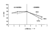
- FIG. 5 shows the conversion efficiency in the low / medium load region and the conversion efficiency in the high load region with carrier frequencies of 5 KHz, 9 KHz, and 13 KHz as parameters.
- the conversion efficiency in the low / medium load region is best at 13 KHz, the next best is 9 KHz, and the lowest is 5 KHz.
- the conversion efficiency in the high load region is best at 5 KHz, the next best is 9 KHz, and the lowest is 13 KHz.
- the power loss includes so-called reactor loss that is the power loss of the reactors 21, 22, and 23 and so-called power loss of the MOSFETs 31 to 36.
- reactor loss There is device loss.
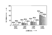
- FIG. 6 shows the reactor loss as parameters with carrier frequencies of 5 KHz, 9 KHz, and 13 KHz. The lower the carrier frequency, the smaller the reactor loss.
- FIG. 7 shows device loss as parameters with carrier frequencies of 5 KHz, 9 KHz, and 13 KHz. The higher the carrier frequency, the smaller the device loss.
- the ratio of the reactor loss and the device loss to the power loss at low / medium load where the power consumption of the brushless DC motor 6 is 25% or 50% of the rated power consumption is the reactor loss. There are more. As for the ratio of the reactor loss and the device loss to the power loss at the time of high load where the power consumption of the brushless DC motor 6 is 75% or 100% of the rated power consumption, the device loss is larger.
- FIG. 8 A modification of the first and second embodiments will be described. As shown in FIG. 8, a series circuit of a reactor 91 and a semiconductor switch 94 is connected in parallel to the reactor 21. A series circuit of a reactor 92 and a semiconductor switch 95 is connected to the reactor 22 in parallel. A series circuit of a reactor 93 and a semiconductor switch 96 is connected to the reactor 23 in parallel.
- the reactors 91, 92, and 93 have smaller inductances than the reactors 21, 22, and 23.
- the semiconductor switches 94, 95, and 96 are opened and closed in response to commands from the controller 90.
- the converter control unit 91 of the controller 90 opens the semiconductor switches 94, 95, and 96 when the load is low / medium.
- the semiconductor switch 94 When the semiconductor switch 94 is opened, the reactor 21 is input to the connection line between the interconnection point of the diodes 31a and 32a and the R phase of the three-phase AC power supply 1, and the reactor 91 is not input.
- the semiconductor switch 95 When the semiconductor switch 95 is opened, the reactor 22 is input to the connection line between the interconnection point of the diodes 33a and 34a and the S phase of the three-phase AC power supply 1, and the reactor 92 is not input.
- the semiconductor switch 96 When the semiconductor switch 96 is opened, the reactor 23 is input to the connection line between the interconnection point of the diodes 35a and 36a and the T phase of the three-phase AC power supply 1, and the reactor 93 is not input.
- the converter control unit 91 of the controller 90 closes the semiconductor switches 94, 95, and 96 when the load is high.
- the semiconductor switch 94 When the semiconductor switch 94 is closed, the parallel circuit of the reactors 21 and 91 is put into the connection line between the interconnection point of the diodes 31 a and 32 a and the R phase of the three-phase AC power supply 1.
- the semiconductor switch 95 When the semiconductor switch 95 is closed, the parallel circuit of the reactors 22 and 92 is put into the connection line between the interconnection point of the diodes 33 a and 34 a and the S phase of the three-phase AC power supply 1.
- the semiconductor switch 96 When the semiconductor switch 96 is closed, the parallel circuit of the reactors 23 and 93 is put into the connection line between the interconnection point of the diodes 35a and 36a and the T phase of the three-phase AC power supply 1.
- the low inductance of the parallel circuit of the reactors 21 and 91, the low inductance of the parallel circuit of the reactors 22 and 92, and the low inductance of the parallel circuit of the reactors 23 and 93 are input to each connection line with the three-phase AC power supply 1.
- an effect of reducing the reactor loss can be obtained.
- the control for changing the modulation factor of the pulse width modulation is performed so that the output voltage of the converter 2 is constant, the number of switchings of the inverter 5 is increased.
- the degree of influence of the switching loss is increased. As a result, the loss is reduced.
- the converter control unit 91 of the controller 90 performs so-called zero current switching that opens and closes the semiconductor switches 94, 95, and 96 while the operation of the converter 2 is stopped. Thereby, the semiconductor switches 94, 95, 96 can be opened and closed without generating an excessive surge voltage / current.
- the zero current switching is performed by detecting current-free periods of R-phase current, S-phase current, and T-phase current in the diode rectification mode as shown in FIG. This can be realized by instructing opening and closing during a non-flow period.
- the magnitude of the load is detected based on the detection results of the current sensors 71, 72, 73.
- the detection of the current sensors 81, 82, 83 on the output side of the inverter 5 is performed.
- the magnitude of the load may be detected based on the result.
- the load is a brushless DC motor
- the load is not limited and can be applied to various electric devices.
- the power converter of the present invention can be used for an air conditioner or the like.
Landscapes
- Engineering & Computer Science (AREA)
- Power Engineering (AREA)
- Rectifiers (AREA)
- Inverter Devices (AREA)
Abstract
コントローラ(90)は、キャリア信号(Eo)を正弦波信号(Er,Es,Et)でパルス幅変調することによりPWM信号(Dr,Ds,Dt)を生成し、生成したPWM信号によりコンバータ(2)のスイッチング素子(31~36)をオン,オフ駆動する。さらに、コントローラ(90)は、前記パルス幅変調の変調条件を負荷(6)の大きさに応じて切換える。このように、負荷(6)の大きさに応じて変調条件を切換えることにより、高調波電流の抑制、昇圧、電源力率の低下を可能としながら電力損失の低減が図れる。
Description
本発明の実施形態は、交流電源の電圧を直流に変換し、変換した直流電圧を所定周波数の交流電圧に変換する電力変換装置に関する。
交流電源の電圧をコンバータで直流に変換し、変換した直流電圧をインバータで所定周波数の交流電圧に変換する電力変換装置が知られている(特開2006-38432号公報)。上記コンバータにおけるスイッチング素子の電力損失は大きく、変換効率向上の妨げとなっている。
リアクタ、ダイオード、スイッチング素子を有し、交流電源の電圧を昇圧および直流変換する昇圧型のコンバータは、スイッチング素子の電力損失が大きいことに加え、上記リアクタの電力損失も大きい。スイッチングをしなければ、変換効率は向上するが、そうすると高調波電流を抑制できなくなるとともに、昇圧ができなくなり、電源力率も低下する。
本発明の実施形態の目的は、高調波電流の抑制、昇圧、および電源力率の低下を可能としながら、電力損失の低減が図れる電力変換装置を提供することである。
請求項1の電力変換装置は、コンバータおよびコントローラを備える。上記コンバータは、交流電源の電圧を昇圧および直流変換する。上記コントローラは、パルス幅変調よりPWM信号を生成し、このPWM信号により前記コンバータを駆動し、かつ前記パルス幅変調の変調条件を当該電力変換装置の負荷に応じて切換える。
[1]第1実施形態
以下、本発明の第1実施形態について図面を参照して説明する。
図1に示すように、商用の三相交流電源1のR相,S相,T相にコンバータ2が接続され、そのコンバータ2の出力端に平滑コンデンサ4が接続される。そして、平滑コンデンサ4にインバータ5が接続され、そのインバータ5の出力端に負荷である例えばブラシレスDCモータ6の相巻線Lu,Lv,Lwが接続される。
以下、本発明の第1実施形態について図面を参照して説明する。
図1に示すように、商用の三相交流電源1のR相,S相,T相にコンバータ2が接続され、そのコンバータ2の出力端に平滑コンデンサ4が接続される。そして、平滑コンデンサ4にインバータ5が接続され、そのインバータ5の出力端に負荷である例えばブラシレスDCモータ6の相巻線Lu,Lv,Lwが接続される。
コンバータ2は、三相交流電源1の電圧を昇圧および直流変換するもので、例えば100Vの交流電圧を300V程度の直流電圧に変換する。また、コンバータ2は、第1,第2ダイオード31a,32aの直列回路、第3,第4ダイオード33a,34aの直列回路、第5,第6ダイオード35a,36aの直列回路を含む。ダイオード31a,32aの相互接続点が三相交流電源1のR相に接続され、ダイオード33a,34aの相互接続点が三相交流電源1のS相に接続され、ダイオード35a,36aの相互接続点が三相交流電源1のT相に接続される。
さらに、コンバータ2は、ダイオード31a,32aの相互接続点と三相交流電源1のR相との接続ラインに挿入接続される第1リアクタ21、ダイオード33a,34aの相互接続点と三相交流電源1のS相との接続ラインに挿入接続される第2リアクタ22、ダイオード35a,36aの相互接続点と三相交流電源1のT相との接続ラインに挿入接続される第3リアクタ23、ダイオード31a~36aにそれぞれ並列接続された第1~第6スイッチング素子たとえばMOSFET(Metal Oxide Semiconductor Field Effect Transistor)31~36を含む。ダイオード31a,33a,35aのカソードが正側出力端2aとなり、ダイオード32a,34a,36aのアノードが負側出力端2bとなる。
なお、ダイオード31a~36aは、MOSFET31~36の寄生ダイオードである。
インバータ5は、MOSFET51,52の直列回路、MOSFET53,54の直列回路、MOSFET55,56の直列回路を含み、これらMOSFET51~56のスイッチングにより、コンバータ2の出力電圧(平滑コンデンサ4の電圧)を所定周波数の三相交流電圧に変換し出力する。MOSFET51,52の相互接続点、MOSFET53,54の相互接続点、MOSFET55,56の相互接続点が、インバータ5の出力端となる。なお、MOSFET51~56は、寄生ダイオード51a~56aを有する。
ブラシレスDCモータ6は、星形結線の相巻線Lu,Lv,Lwを有する固定子、および永久磁石を有する回転子により構成される。相巻線Lu,Lv,Lwに電流が流れることにより生じる磁界と永久磁石が作る磁界との相互作用により、回転子が回転する。相巻線LuがMOSFET51,52の相互接続点に接続され、相巻線LvがMOSFET53,54の相互接続点に接続され、相巻線LwがMOSFET55,56の相互接続点に接続される。
三相交流電源1とリアクタ21,22,23との間の通電路に、入力電流検知用の電流センサ71,72,73が配設される。インバータ5の出力端とブラシレスDCモータ6との間の通電路に、出力電流(相巻線電流)検知用の電流センサ81,82,83が配設される。これら電流センサの検知結果がコントローラ90に供給される。
コントローラ90は、主要な機能としてコンバータ制御部91およびインバータ制御部92を含む。
コンバータ制御部91は、所定周波数のキャリア信号(三角波信号)Eoを正弦波信号Er,Es,Etでパルス幅変調(PWM)することにより、つまりキャリア信号Eoの電圧と正弦波信号Er,Es,Etの電圧との比較により、PWM信号Dr,Ds,Dtを生成する。さらに、コンバータ制御部91は、生成したPWM信号Dr,Ds,Dtによりコンバータ2のMOSFET31~36をオン,オフ駆動し、かつ上記パルス幅変調の変調条件(変調率)を当該電力変換装置の負荷の大きさに応じて切換える。負荷の大きさとは、ブラシレスDCモータ6の消費電力のことである。正弦波信号Er,Es,Etは、三相交流電源1のR相電圧、S相電圧、T相電圧の周期に同期するもので、電流センサ71,72,73の検知結果に基づいてコンバータ制御部91により生成される。
コンバータ制御部91は、所定周波数のキャリア信号(三角波信号)Eoを正弦波信号Er,Es,Etでパルス幅変調(PWM)することにより、つまりキャリア信号Eoの電圧と正弦波信号Er,Es,Etの電圧との比較により、PWM信号Dr,Ds,Dtを生成する。さらに、コンバータ制御部91は、生成したPWM信号Dr,Ds,Dtによりコンバータ2のMOSFET31~36をオン,オフ駆動し、かつ上記パルス幅変調の変調条件(変調率)を当該電力変換装置の負荷の大きさに応じて切換える。負荷の大きさとは、ブラシレスDCモータ6の消費電力のことである。正弦波信号Er,Es,Etは、三相交流電源1のR相電圧、S相電圧、T相電圧の周期に同期するもので、電流センサ71,72,73の検知結果に基づいてコンバータ制御部91により生成される。
インバータ制御部92は、所定周波数のキャリア信号(三角波信号)Eioを正弦波信号Eu,Ev,Ewでパルス幅変調(PWM)することにより、つまりキャリア信号Eioの電圧と正弦波信号Eu,Ev,Ewの電圧との比較により、PWM信号Du,Dv,Dwを生成する。さらに、インバータ制御部92は、生成したPWM信号Du,Dv,Dwによりインバータ5のMOSFET51~56をオン,オフ駆動する。正弦波信号Eu,Ev,Ewは、ブラシレスDCモータの相巻線Lu,Lv,Lwに誘起する電圧の周期に同期するもので、電流センサ81,82,83の検知結果に基づいてインバータ制御部92により生成される。
つぎに、コンバータ2の動作について説明する。
三相交流電源1のR相電圧が正レベルとなる位相では、三相交流電源1からリアクタ21および正側ダイオード31aを通って平滑コンデンサ4に電流が流れる。平滑コンデンサ4を経た電流は、先ず負側ダイオード34aおよびリアクタ22を通って三相交流電源1のS相に戻り、次にR相電圧の位相が進むにつれ、負側ダイオード36aおよびリアクタ23を通って三相交流電源1のT相に戻る。同じく三相交流電源1のR相電圧が正レベルとなる位相では、コンバータ制御部91で生成されるPWM信号Duに応じてMOSFET32がオン,オフを繰り返す。MOSFET32のオン時、ダイオード31a,32aの相互接続点がコンバータ2の負側出力端2bと導通し、三相交流電源1に対してリアクタ21、MOSFET32、負側ダイオード34a、リアクタ22を介した短絡路が形成される。この短絡路の形成により、リアクタ21,22にエネルギ(電荷)が蓄えられる。リアクタ21,22に蓄えられたエネルギは、MOSFET32のオフ時に平滑コンデンサ4に供給される。このエネルギ供給により、昇圧がなされる。
三相交流電源1のR相電圧が正レベルとなる位相では、三相交流電源1からリアクタ21および正側ダイオード31aを通って平滑コンデンサ4に電流が流れる。平滑コンデンサ4を経た電流は、先ず負側ダイオード34aおよびリアクタ22を通って三相交流電源1のS相に戻り、次にR相電圧の位相が進むにつれ、負側ダイオード36aおよびリアクタ23を通って三相交流電源1のT相に戻る。同じく三相交流電源1のR相電圧が正レベルとなる位相では、コンバータ制御部91で生成されるPWM信号Duに応じてMOSFET32がオン,オフを繰り返す。MOSFET32のオン時、ダイオード31a,32aの相互接続点がコンバータ2の負側出力端2bと導通し、三相交流電源1に対してリアクタ21、MOSFET32、負側ダイオード34a、リアクタ22を介した短絡路が形成される。この短絡路の形成により、リアクタ21,22にエネルギ(電荷)が蓄えられる。リアクタ21,22に蓄えられたエネルギは、MOSFET32のオフ時に平滑コンデンサ4に供給される。このエネルギ供給により、昇圧がなされる。
三相交流電源1のS相電圧が正レベルとなる位相では、三相交流電源1からリアクタ22および正側ダイオード33aを通って平滑コンデンサ4に電流が流れる。平滑コンデンサ4を経た電流は、先ず負側ダイオード36aおよびリアクタ23を通って三相交流電源1のT相に戻り、次にS相電圧の位相が進むにつれ、負側ダイオード32aおよびリアクタ21を通って三相交流電源1のR相に戻る。同じく三相交流電源1のS相電圧が正レベルとなる位相では、コンバータ制御部91で生成されるPWM信号Dvに応じてMOSFET34がオン,オフを繰り返す。MOSFET34のオン時、ダイオード33a,34aの相互接続点がコンバータ2の負側出力端と導通し、三相交流電源1に対してリアクタ22、MOSFET34、負側ダイオード36a、リアクタ23を介した短絡路が形成される。この短絡路の形成により、リアクタ22,23にエネルギ(電荷)が蓄えられる。リアクタ22,23に蓄えられたエネルギは、MOSFET34のオフ時に平滑コンデンサ4に供給される。このエネルギ供給により、昇圧がなされる。
三相交流電源1のT相電圧が正レベルとなる位相では、三相交流電源1からリアクタ23および正側ダイオード35aを通って平滑コンデンサ4に電流が流れる。平滑コンデンサ4を経た電流は、先ず負側ダイオード32aおよびリアクタ21を通って三相交流電源1のR相に戻り、次にT相電圧の位相が進むにつれ、負側ダイオード34aおよびリアクタ22を通って三相交流電源1のS相に戻る。同じく三相交流電源1のT相電圧が正レベルとなる位相では、コンバータ制御部91で生成されるPWM信号Dwに応じてMOSFET36がオン,オフを繰り返す。MOSFET36のオン時、ダイオード35a,36aの相互接続点がコンバータ2の負側出力端と導通し、三相交流電源1に対してリアクタ23、MOSFET36、負側ダイオード32a、リアクタ21を介した短絡路が形成される。この短絡路の形成により、リアクタ23,21にエネルギ(電荷)が蓄えられる。リアクタ23,21に蓄えられたエネルギは、MOSFET36のオフ時に平滑コンデンサ4に供給される。このエネルギ供給により、昇圧がなされる。
R相入力電圧,S相入力電圧,T相入力電圧のそれぞれが負レベルとなる位相では、正側ダイオード31a,33a,35aに並列接続されているMOSFET31,33,35がオン,オフを繰り返す。これらMOSFET31,33,35のオン,オフに伴う動作については、正負が反対となるだけで、基本的には正レベル期間と同じ動作パターンとなる。よって、その詳細な説明は省略する。
つぎに、コントローラ90が実行する制御を図2のフローチャートに示す。
コントローラ90は、図2のフローチャートに示すように、当該電力変換装置の負荷の大きさ(ブラシレスDCモータ6の消費電力)を電流センサ71,72,73の検知電流(入力電流)から検出する(ステップS1)。そして、コントローラ90は、検出した負荷の大きさが、高負荷であるか低・中負荷であるかを判定する(ステップS2)。例えば、ブラシレスDCモータ6の消費電力が定格消費電力の75%以上の場合、コンバータ制御部91は、負荷が高負荷であると判定する。ブラシレスDCモータ6の消費電力が定格消費電力の75%未満の場合、コンバータ制御部91は、負荷が低・中負荷であると判定する。
コントローラ90は、図2のフローチャートに示すように、当該電力変換装置の負荷の大きさ(ブラシレスDCモータ6の消費電力)を電流センサ71,72,73の検知電流(入力電流)から検出する(ステップS1)。そして、コントローラ90は、検出した負荷の大きさが、高負荷であるか低・中負荷であるかを判定する(ステップS2)。例えば、ブラシレスDCモータ6の消費電力が定格消費電力の75%以上の場合、コンバータ制御部91は、負荷が高負荷であると判定する。ブラシレスDCモータ6の消費電力が定格消費電力の75%未満の場合、コンバータ制御部91は、負荷が低・中負荷であると判定する。
上記判定結果が高負荷の場合(ステップS2のYES)、コントローラ90は、パルス幅変調の変調率を“2”未満の例えば“1”に設定する(ステップS3)。
変調率“1”は、図3に示すように、キャリア信号Eoと同じ最大電圧レベルを有する正弦波信号Eu,Ev,Erを生成し、その正弦波信号Eu,Ev,Erによってキャリア信号Eoをパルス幅変調することである。この変調率“1”のパルス幅変調により、3つの相のMOSFETを共にスイッチングするための3相スイッチングモードのPWM信号Du,Dv,Dwが得られる。
高調波電流の悪化が懸念される高負荷領域では、この3相スイッチングモードを選択して3つの相のMOSFETのオン,オフを繰り返すことにより、コンバータ2への入力電流に含まれる高調波電流を抑制できるとともに、コンバータ2の十分な昇圧作用が得られる。なお、パルス幅変調の変調率が小さいほど、コンバータ2の昇圧レベルが大きくなる。
なお、変調率“1”に代えて、変調率“1.1”~“1.9”のいずれかを設定してもよい。変調率“1.1”~“1.9”のいずれかを設定した場合、2つの相のMOSFETを共にスイッチングして残りの1つの相のMOSFETはスイッチングさせない2相スイッチングモードのPWM信号Du,Dv,Dwが得られる。この2相スイッチングモードを採用した場合でも、コンバータ2への入力電流に含まれる高調波電流を抑制できるとともに、コンバータ2の十分な昇圧作用が得られる。
一方、上記判定結果が低・中負荷の場合(ステップS2のNO)、コントローラ90は、パルス幅変調の変調率を“2”以上の例えば“2”に設定する(ステップS4)。
変調率“2”は、図4に示すように、キャリア信号Eoの2倍の最大電圧レベルを有する正弦波信号Eu,Ev,Erを生成し、その正弦波信号Eu,Ev,Erによってキャリア信号Eoをパルス幅変調することである。パルス幅変調の変調率が“2”以上の場合、1つの相のMOSFETをスイッチングして残りの2つの相のMOSFETはスイッチングさせない1相スイッチングモードのPWM信号Du,Dv,Dwが得られる。
1相スイッチングモードの場合、R相電圧,S相電圧,T相電圧が正レベルとなる位相の前縁側期間および後縁側期間においてMOSFET32,34,36がオン,オフし、R相電圧,S相電圧,T相電圧が負レベルとなる位相の前縁側期間および後縁側期間においてMOSFET31,33,35がオン,オフを繰り返すので、コンバータ2への入力電流の波形を正弦波に追従性よく近似させることができる。これにより、電源力率が向上する。ただし、コンバータ2の昇圧効果は、少ないか、もしくはほとんど得られない。
また、1相スイッチングモードの場合は、MOSFET31~36のオン,オフ回数が少ないので、MOSFET31~36およびリアクタ21,22,23における電力損失も低減する。
このように、負荷の大きさに応じて変調率を切換えることにより、高調波電流の抑制、昇圧、電源力率の低下を可能としながら電力損失の低減が図れる。ひいては、低・中負荷から高負荷まで全運転域の変換効率が向上する。
[2]第2実施形態
本発明の第2実施形態について説明する。
コントローラ90のコンバータ制御部91は、コンバータ2の出力電圧が一定となるようにパルス幅変調の変調率を変更しながら、コンバータ2のパルス幅変調の変調条件としてキャリア信号Eoの周波数(キャリア周波数という)を当該電力変換装置の負荷の大きさに応じて切換える。コンバータ2の出力電圧が一定となるようにパルス幅変調の変調率を変更する制御とは、負荷が小さい場合は変調率を大きくし、負荷が大きい場合は変調率を小さくする制御である。
他の構成は第1実施形態と同じなので、その説明は省略する。
本発明の第2実施形態について説明する。
コントローラ90のコンバータ制御部91は、コンバータ2の出力電圧が一定となるようにパルス幅変調の変調率を変更しながら、コンバータ2のパルス幅変調の変調条件としてキャリア信号Eoの周波数(キャリア周波数という)を当該電力変換装置の負荷の大きさに応じて切換える。コンバータ2の出力電圧が一定となるようにパルス幅変調の変調率を変更する制御とは、負荷が小さい場合は変調率を大きくし、負荷が大きい場合は変調率を小さくする制御である。
他の構成は第1実施形態と同じなので、その説明は省略する。
すなわち、コンバータ制御部91は、低・中負荷領域では高キャリア周波数たとえば13KHzを設定し、高負荷領域では低キャリア周波数たとえば5KHzを設定する。
高キャリア周波数を設定した場合、生成されるPWM信号Dr,Ds,Dtの周波数が高くなり、それに伴ってMOSFET31~36のオン,オフ回数が多くなる。低キャリア周波数を設定した場合、生成されるPWM信号Dr,Ds,Dtの周波数が低くなり、それに伴ってMOSFET31~36のオン,オフ回数が少なくなる。
低・中負荷領域の変換効率と高負荷領域の変換効率とをキャリア周波数5KHz,9KHz,13KHzをパラメータとして示したのが図5である。低・中負荷領域の変換効率は、13KHzが最も良く、次に良いのが9KHz、最も低いのが5KHzである。高負荷領域の変換効率は、5KHzが最も良く、次に良いのが9KHz、最も低いのが13KHzである。
このように負荷およびキヤリア周波数に応じて変換効率が変化する理由を検討すると、電力損失には、リアクタ21,22,23の電力損失であるいわゆるリアクタ損失、およびMOSFET31~36の電力損失であるいわゆるデバイス損失がある。このうち、リアクタ損失をキャリア周波数5KHz,9KHz,13KHzをパラメータとして示したのが図6であり、キャリア周波数が低いほどリアクタ損失が小さくなる。一方、デバイス損失をキャリア周波数5KHz,9KHz,13KHzをパラメータとして示したのが図7であり、キャリア周波数が高いほどデバイス損失が小さくなる。
図6および図7から分かるように、ブラシレスDCモータ6の消費電力が定格消費電力の25%や50%である低・中負荷時の電力損失に占めるリアクタ損失とデバイス損失の割合は、リアクタ損失の方が多い。ブラシレスDCモータ6の消費電力が定格消費電力の75%や100%である高負荷時の電力損失に占めるリアクタ損失とデバイス損失の割合は、デバイス損失の方が多い。
これらの点を考慮すると、低・中負荷領域では、デバイス損失の低減を目指したほうが変換効率低減に効果的であることから、リアクタ損失がより小さくなる高キャリア周波数13KHzを選定するのがよい。高負荷領域では、デバイス損失の低減を目指したほうが変換効率低減に効果的であることから、デバイス損失がより小さくなる低キャリア周波数5KHzを選定するのがよい。
このように、負荷の大きさに応じてキャリア周波数を切換えることにより、低・中負荷から高負荷まで全運転域の変換効率が向上する。
[3]第1および第2実施形態の変形例について説明する。
図8に示すように、リアクタ21に対し、リアクタ91と半導体スイッチ94との直列回路が並列接続される。リアクタ22に対し、リアクタ92と半導体スイッチ95との直列回路が並列接続される。リアクタ23に対し、リアクタ93と半導体スイッチ96との直列回路が並列接続される。
図8に示すように、リアクタ21に対し、リアクタ91と半導体スイッチ94との直列回路が並列接続される。リアクタ22に対し、リアクタ92と半導体スイッチ95との直列回路が並列接続される。リアクタ23に対し、リアクタ93と半導体スイッチ96との直列回路が並列接続される。
リアクタ91,92,93は、リアクタ21,22,23よりもインダクタンスが小さい。半導体スイッチ94,95,96は、コントローラ90の指令に応じて開閉する。
コントローラ90のコンバータ制御部91は、低・中負荷時、半導体スイッチ94,95,96を開く。半導体スイッチ94が開くと、ダイオード31a,32aの相互接続点と三相交流電源1のR相との接続ラインに、リアクタ21が投入されてリアクタ91は投入されない。半導体スイッチ95が開くと、ダイオード33a,34aの相互接続点と三相交流電源1のS相との接続ラインに、リアクタ22が投入されてリアクタ92は投入されない。半導体スイッチ96が開くと、ダイオード35a,36aの相互接続点と三相交流電源1のT相との接続ラインに、リアクタ23が投入されてリアクタ93は投入されない。
このように、リアクタ21,22,23のそれぞれ高インダクタンスを三相交流電源1との各接続ラインに投入することにより、高調波電流の抑制効果が向上する。この場合、コンバータ2の出力電圧が一定となるようにパルス幅変調の変調率を変更する制御を実行することにより、コンバータ2のスイッチング回数を低減できてデバイス損失の低減効果が得られる。
コントローラ90のコンバータ制御部91は、高負荷時、半導体スイッチ94,95,96を閉じる。半導体スイッチ94が閉じると、ダイオード31a,32aの相互接続点と三相交流電源1のR相との接続ラインに、リアクタ21,91の並列回路が投入される。半導体スイッチ95が閉じると、ダイオード33a,34aの相互接続点と三相交流電源1のS相との接続ラインに、リアクタ22,92の並列回路が投入される。半導体スイッチ96が閉じると、ダイオード35a,36aの相互接続点と三相交流電源1のT相との接続ラインに、リアクタ23,93の並列回路が投入される。
このように、リアクタ21,91の並列回路の低インダクタンス、リアクタ22,92の並列回路の低インダクタンス、リアクタ23,93の並列回路の低インダクタンスを三相交流電源1との各接続ラインに投入することにより、リアクタ損失の低減効果が得られる。この場合、コンバータ2の出力電圧が一定となるようにパルス幅変調の変調率を変更する制御を実行すると、インバータ5のスイッチング回数を増加させることになるが、高負荷領域ではスイッチング損失の影響度が低下するため、結果として低損失化につながる。
また、コントローラ90のコンバータ制御部91は、半導体スイッチ94,95,96をコンバータ2の動作停止中に開閉するいわゆる零電流スイッチングを行う。これにより、過大なサージ電圧/電流の発生を生じることなく、半導体スイッチ94,95,96を開閉できる。零電流スイッチングは、具体的には、図9に示すようなダイオード整流モードにおけるR相電流,S相電流,T相電流の無通流期間を電流センサ71,72,73により検出し、検出した無通流期間において開閉を指令することで実現できる。
[4]他の変形例
上記各実施形態では、電流センサ71,72,73の検知結果に基づいて負荷の大きさを検出したが、インバータ5の出力側の電流センサ81,82,83の検知結果に基づいて負荷の大きさを検出してもよい。
上記各実施形態では、電流センサ71,72,73の検知結果に基づいて負荷の大きさを検出したが、インバータ5の出力側の電流センサ81,82,83の検知結果に基づいて負荷の大きさを検出してもよい。
上記各実施形態では、負荷がブラシレスDCモータである場合を例に説明したが、負荷に限定はなく、種々の電気機器への適用が可能である。
上記各実施形態および変形例は、例として提示したものであり、発明の範囲を限定することは意図していない。この新規な各実施形態および変形例は、その他の様々な形態で実施されることが可能であり、発明の要旨を逸脱しない範囲で、種々の省略、書き換え、変更を行うことができる。これら実施形態や変形は、発明の範囲は要旨に含まれるとともに、請求の範囲に記載された発明とその均等の範囲に含まれる。
本発明の電力変換装置は、空気調和機等への利用が可能である。
Claims (5)
- 交流電源の電圧を昇圧および直流変換するコンバータと、
パルス幅変調よりPWM信号を生成し、このPWM信号により前記コンバータを駆動し、かつ前記パルス幅変調の変調条件を当該電力変換装置の負荷に応じて切換えるコントローラと、
を備えることを特徴とする電力変換装置。 - 前記コントローラは、前記パルス幅変調の変調率を前記負荷の大きさに応じて切換えることを特徴とする請求項1記載の電力変換装置。
- 前記コントローラは、キャリア信号を正弦波信号でパルス幅変調することにより前記PWM信号を生成し、このPWM信号により前記コンバータを駆動し、かつ前記キャリア信号の周波数を前記負荷の大きさに応じて切換えることを特徴とする請求項1記載の電力変換装置。
- 前記交流電源は、三相交流電源であり、
前記コンバータは、第1および第2ダイオードの直列回路、第3および第4ダイオードの直列回路、第5および第6ダイオードの直列回路、前記三相交流電源のR相と前記第1,第2ダイオードの相互接続点との間に接続される第1リアクタ、前記三相交流電源のS相と前記第3,第4ダイオードの相互接続点との間に接続される第2リアクタ、前記三相交流電源のT相と前記第5,第6ダイオードの相互接続点との間に接続される第3リアクタ、前記第1~第6ダイオードにそれぞれ並列接続された第1~第6スイッチング素子を含み、前記第1,第3,第5ダイオードのカソードを正側出力端とし、前記第2,第4,第6ダイオードのアノードを負側出力端とする、
ことを特徴とする請求項1乃至請求項3のいずれか記載の電力変換装置。 - 前記コンバータの出力電圧を所定周波数の交流電圧に変換するインバータ、
をさらに備え、
前記負荷は、前記インバータの出力により動作する、
ことを特徴とする請求項1乃至請求項3のいずれか記載の電力変換装置。
Priority Applications (1)
| Application Number | Priority Date | Filing Date | Title |
|---|---|---|---|
| JP2015556714A JPWO2015104886A1 (ja) | 2014-01-09 | 2014-10-28 | 電力変換装置 |
Applications Claiming Priority (2)
| Application Number | Priority Date | Filing Date | Title |
|---|---|---|---|
| JP2014-002625 | 2014-01-09 | ||
| JP2014002625 | 2014-01-09 |
Publications (1)
| Publication Number | Publication Date |
|---|---|
| WO2015104886A1 true WO2015104886A1 (ja) | 2015-07-16 |
Family
ID=53523728
Family Applications (1)
| Application Number | Title | Priority Date | Filing Date |
|---|---|---|---|
| PCT/JP2014/078622 Ceased WO2015104886A1 (ja) | 2014-01-09 | 2014-10-28 | 電力変換装置 |
Country Status (2)
| Country | Link |
|---|---|
| JP (1) | JPWO2015104886A1 (ja) |
| WO (1) | WO2015104886A1 (ja) |
Cited By (6)
| Publication number | Priority date | Publication date | Assignee | Title |
|---|---|---|---|---|
| CN105656319A (zh) * | 2016-02-04 | 2016-06-08 | 浙江雷亚电子有限公司 | 一种基于输出电路功率因数测控的逆变控制器 |
| JP2017073870A (ja) * | 2015-10-06 | 2017-04-13 | 東芝キヤリア株式会社 | 電力変換装置 |
| JP2017112776A (ja) * | 2015-12-18 | 2017-06-22 | 三菱重工業株式会社 | コンバータ装置、駆動制御装置、モータ、およびコンプレッサ |
| JP2017123706A (ja) * | 2016-01-05 | 2017-07-13 | 東芝三菱電機産業システム株式会社 | 電力変換装置及びその制御方法 |
| WO2018185813A1 (ja) * | 2017-04-03 | 2018-10-11 | 東芝三菱電機産業システム株式会社 | 電力変換装置 |
| JP2022061626A (ja) * | 2020-10-07 | 2022-04-19 | 東芝キヤリア株式会社 | 電力変換装置 |
Citations (6)
| Publication number | Priority date | Publication date | Assignee | Title |
|---|---|---|---|---|
| JPH07213067A (ja) * | 1994-01-24 | 1995-08-11 | Fuji Electric Co Ltd | Pwmコンバータの制御回路 |
| JPH09252581A (ja) * | 1996-03-14 | 1997-09-22 | Hitachi Ltd | 無停電電源装置の運転方法 |
| JPH1028378A (ja) * | 1996-07-11 | 1998-01-27 | Toshiba Corp | 電力変換装置の制御方法及び電力変換システムの制御方法 |
| JPH1042565A (ja) * | 1996-07-18 | 1998-02-13 | Mitsubishi Electric Corp | Pwmコンバータ装置の起動回路 |
| JPH11215849A (ja) * | 1998-01-28 | 1999-08-06 | Hitachi Ltd | パルス幅変調電力変換装置 |
| JP2010200412A (ja) * | 2009-02-23 | 2010-09-09 | Fanuc Ltd | Pwm整流器 |
-
2014
- 2014-10-28 JP JP2015556714A patent/JPWO2015104886A1/ja active Pending
- 2014-10-28 WO PCT/JP2014/078622 patent/WO2015104886A1/ja not_active Ceased
Patent Citations (6)
| Publication number | Priority date | Publication date | Assignee | Title |
|---|---|---|---|---|
| JPH07213067A (ja) * | 1994-01-24 | 1995-08-11 | Fuji Electric Co Ltd | Pwmコンバータの制御回路 |
| JPH09252581A (ja) * | 1996-03-14 | 1997-09-22 | Hitachi Ltd | 無停電電源装置の運転方法 |
| JPH1028378A (ja) * | 1996-07-11 | 1998-01-27 | Toshiba Corp | 電力変換装置の制御方法及び電力変換システムの制御方法 |
| JPH1042565A (ja) * | 1996-07-18 | 1998-02-13 | Mitsubishi Electric Corp | Pwmコンバータ装置の起動回路 |
| JPH11215849A (ja) * | 1998-01-28 | 1999-08-06 | Hitachi Ltd | パルス幅変調電力変換装置 |
| JP2010200412A (ja) * | 2009-02-23 | 2010-09-09 | Fanuc Ltd | Pwm整流器 |
Cited By (7)
| Publication number | Priority date | Publication date | Assignee | Title |
|---|---|---|---|---|
| JP2017073870A (ja) * | 2015-10-06 | 2017-04-13 | 東芝キヤリア株式会社 | 電力変換装置 |
| JP2017112776A (ja) * | 2015-12-18 | 2017-06-22 | 三菱重工業株式会社 | コンバータ装置、駆動制御装置、モータ、およびコンプレッサ |
| JP2017123706A (ja) * | 2016-01-05 | 2017-07-13 | 東芝三菱電機産業システム株式会社 | 電力変換装置及びその制御方法 |
| CN105656319A (zh) * | 2016-02-04 | 2016-06-08 | 浙江雷亚电子有限公司 | 一种基于输出电路功率因数测控的逆变控制器 |
| WO2018185813A1 (ja) * | 2017-04-03 | 2018-10-11 | 東芝三菱電機産業システム株式会社 | 電力変換装置 |
| JP2022061626A (ja) * | 2020-10-07 | 2022-04-19 | 東芝キヤリア株式会社 | 電力変換装置 |
| JP7471991B2 (ja) | 2020-10-07 | 2024-04-22 | 東芝キヤリア株式会社 | 電力変換装置 |
Also Published As
| Publication number | Publication date |
|---|---|
| JPWO2015104886A1 (ja) | 2017-03-23 |
Similar Documents
| Publication | Publication Date | Title |
|---|---|---|
| US9374016B2 (en) | AC-DC converter | |
| TWI643439B (zh) | Power conversion device and three-phase AC power supply device | |
| US9887638B2 (en) | Power conversion apparatus with frequency operation change based on input voltage | |
| US10439542B2 (en) | Electric power conversion device | |
| TWI509256B (zh) | Polarity detection circuit | |
| CN106471725B (zh) | 直接型交流电力变换装置 | |
| WO2015104886A1 (ja) | 電力変換装置 | |
| EP3182574B1 (en) | Converter unit, drive controller, motor, and compressor | |
| US9742272B2 (en) | AC-DC converter | |
| CN101584107A (zh) | 直流电源装置和具有该直流电源装置的空气调节器 | |
| KR101457569B1 (ko) | 정류 회로 및 그것을 이용한 모터 구동 장치 | |
| CN104205605A (zh) | 逆变器装置 | |
| JP5678860B2 (ja) | 交流直流変換器 | |
| US9780691B1 (en) | AC-DC power conversion apparatus to output boosted DC voltage | |
| JPWO2014167727A1 (ja) | 電力変換装置 | |
| JP5471384B2 (ja) | 電動機駆動用インバータ装置 | |
| JP6184885B2 (ja) | インバータ装置及び空気調和機 | |
| JPWO2019073904A1 (ja) | Ac−acコンバータ回路 | |
| CN106602870B (zh) | 功率转换方法和功率转换器 | |
| JP6301270B2 (ja) | モータ駆動装置 | |
| JP2019508008A (ja) | エネルギー回生型整流装置 | |
| JPWO2016104328A1 (ja) | モータ駆動装置 | |
| EP4693875A1 (en) | Converter device and motor drive device equipped with same | |
| JP2008099348A (ja) | Dc−dcコンバータ | |
| Singh et al. | Three-phase electric drive with modified electronic smoothing inductor |
Legal Events
| Date | Code | Title | Description |
|---|---|---|---|
| 121 | Ep: the epo has been informed by wipo that ep was designated in this application |
Ref document number: 14878031 Country of ref document: EP Kind code of ref document: A1 |
|
| ENP | Entry into the national phase |
Ref document number: 2015556714 Country of ref document: JP Kind code of ref document: A |
|
| NENP | Non-entry into the national phase |
Ref country code: DE |
|
| 122 | Ep: pct application non-entry in european phase |
Ref document number: 14878031 Country of ref document: EP Kind code of ref document: A1 |