WO2015093229A1 - 配線基板材料のデスミア処理方法、配線基板材料の製造方法および複合絶縁層形成材料 - Google Patents
配線基板材料のデスミア処理方法、配線基板材料の製造方法および複合絶縁層形成材料 Download PDFInfo
- Publication number
- WO2015093229A1 WO2015093229A1 PCT/JP2014/080914 JP2014080914W WO2015093229A1 WO 2015093229 A1 WO2015093229 A1 WO 2015093229A1 JP 2014080914 W JP2014080914 W JP 2014080914W WO 2015093229 A1 WO2015093229 A1 WO 2015093229A1
- Authority
- WO
- WIPO (PCT)
- Prior art keywords
- wiring board
- insulating layer
- consumable
- layer
- board material
- Prior art date
- Legal status (The legal status is an assumption and is not a legal conclusion. Google has not performed a legal analysis and makes no representation as to the accuracy of the status listed.)
- Ceased
Links
Images





Classifications
-
- H—ELECTRICITY
- H05—ELECTRIC TECHNIQUES NOT OTHERWISE PROVIDED FOR
- H05K—PRINTED CIRCUITS; CASINGS OR CONSTRUCTIONAL DETAILS OF ELECTRIC APPARATUS; MANUFACTURE OF ASSEMBLAGES OF ELECTRICAL COMPONENTS
- H05K3/00—Apparatus or processes for manufacturing printed circuits
- H05K3/0011—Working of insulating substrates or insulating layers
- H05K3/0055—After-treatment, e.g. cleaning or desmearing of holes
-
- B—PERFORMING OPERATIONS; TRANSPORTING
- B32—LAYERED PRODUCTS
- B32B—LAYERED PRODUCTS, i.e. PRODUCTS BUILT-UP OF STRATA OF FLAT OR NON-FLAT, e.g. CELLULAR OR HONEYCOMB, FORM
- B32B15/00—Layered products comprising a layer of metal
- B32B15/04—Layered products comprising a layer of metal comprising metal as the main or only constituent of a layer, which is next to another layer of the same or of a different material
- B32B15/08—Layered products comprising a layer of metal comprising metal as the main or only constituent of a layer, which is next to another layer of the same or of a different material of synthetic resin
-
- B—PERFORMING OPERATIONS; TRANSPORTING
- B32—LAYERED PRODUCTS
- B32B—LAYERED PRODUCTS, i.e. PRODUCTS BUILT-UP OF STRATA OF FLAT OR NON-FLAT, e.g. CELLULAR OR HONEYCOMB, FORM
- B32B15/00—Layered products comprising a layer of metal
- B32B15/20—Layered products comprising a layer of metal comprising aluminium or copper
-
- B—PERFORMING OPERATIONS; TRANSPORTING
- B32—LAYERED PRODUCTS
- B32B—LAYERED PRODUCTS, i.e. PRODUCTS BUILT-UP OF STRATA OF FLAT OR NON-FLAT, e.g. CELLULAR OR HONEYCOMB, FORM
- B32B27/00—Layered products comprising a layer of synthetic resin
- B32B27/06—Layered products comprising a layer of synthetic resin as the main or only constituent of a layer, which is next to another layer of the same or of a different material
-
- B—PERFORMING OPERATIONS; TRANSPORTING
- B32—LAYERED PRODUCTS
- B32B—LAYERED PRODUCTS, i.e. PRODUCTS BUILT-UP OF STRATA OF FLAT OR NON-FLAT, e.g. CELLULAR OR HONEYCOMB, FORM
- B32B27/00—Layered products comprising a layer of synthetic resin
- B32B27/06—Layered products comprising a layer of synthetic resin as the main or only constituent of a layer, which is next to another layer of the same or of a different material
- B32B27/08—Layered products comprising a layer of synthetic resin as the main or only constituent of a layer, which is next to another layer of the same or of a different material of synthetic resin
-
- B—PERFORMING OPERATIONS; TRANSPORTING
- B32—LAYERED PRODUCTS
- B32B—LAYERED PRODUCTS, i.e. PRODUCTS BUILT-UP OF STRATA OF FLAT OR NON-FLAT, e.g. CELLULAR OR HONEYCOMB, FORM
- B32B27/00—Layered products comprising a layer of synthetic resin
- B32B27/28—Layered products comprising a layer of synthetic resin comprising synthetic resins not wholly covered by any one of the sub-groups B32B27/30 - B32B27/42
-
- B—PERFORMING OPERATIONS; TRANSPORTING
- B32—LAYERED PRODUCTS
- B32B—LAYERED PRODUCTS, i.e. PRODUCTS BUILT-UP OF STRATA OF FLAT OR NON-FLAT, e.g. CELLULAR OR HONEYCOMB, FORM
- B32B27/00—Layered products comprising a layer of synthetic resin
- B32B27/28—Layered products comprising a layer of synthetic resin comprising synthetic resins not wholly covered by any one of the sub-groups B32B27/30 - B32B27/42
- B32B27/281—Layered products comprising a layer of synthetic resin comprising synthetic resins not wholly covered by any one of the sub-groups B32B27/30 - B32B27/42 comprising polyimides
-
- B—PERFORMING OPERATIONS; TRANSPORTING
- B32—LAYERED PRODUCTS
- B32B—LAYERED PRODUCTS, i.e. PRODUCTS BUILT-UP OF STRATA OF FLAT OR NON-FLAT, e.g. CELLULAR OR HONEYCOMB, FORM
- B32B27/00—Layered products comprising a layer of synthetic resin
- B32B27/30—Layered products comprising a layer of synthetic resin comprising vinyl (co)polymers; comprising acrylic (co)polymers
-
- B—PERFORMING OPERATIONS; TRANSPORTING
- B32—LAYERED PRODUCTS
- B32B—LAYERED PRODUCTS, i.e. PRODUCTS BUILT-UP OF STRATA OF FLAT OR NON-FLAT, e.g. CELLULAR OR HONEYCOMB, FORM
- B32B27/00—Layered products comprising a layer of synthetic resin
- B32B27/30—Layered products comprising a layer of synthetic resin comprising vinyl (co)polymers; comprising acrylic (co)polymers
- B32B27/308—Layered products comprising a layer of synthetic resin comprising vinyl (co)polymers; comprising acrylic (co)polymers comprising acrylic (co)polymers
-
- B—PERFORMING OPERATIONS; TRANSPORTING
- B32—LAYERED PRODUCTS
- B32B—LAYERED PRODUCTS, i.e. PRODUCTS BUILT-UP OF STRATA OF FLAT OR NON-FLAT, e.g. CELLULAR OR HONEYCOMB, FORM
- B32B27/00—Layered products comprising a layer of synthetic resin
- B32B27/32—Layered products comprising a layer of synthetic resin comprising polyolefins
-
- B—PERFORMING OPERATIONS; TRANSPORTING
- B32—LAYERED PRODUCTS
- B32B—LAYERED PRODUCTS, i.e. PRODUCTS BUILT-UP OF STRATA OF FLAT OR NON-FLAT, e.g. CELLULAR OR HONEYCOMB, FORM
- B32B27/00—Layered products comprising a layer of synthetic resin
- B32B27/36—Layered products comprising a layer of synthetic resin comprising polyesters
-
- B—PERFORMING OPERATIONS; TRANSPORTING
- B32—LAYERED PRODUCTS
- B32B—LAYERED PRODUCTS, i.e. PRODUCTS BUILT-UP OF STRATA OF FLAT OR NON-FLAT, e.g. CELLULAR OR HONEYCOMB, FORM
- B32B27/00—Layered products comprising a layer of synthetic resin
- B32B27/38—Layered products comprising a layer of synthetic resin comprising epoxy resins
-
- B—PERFORMING OPERATIONS; TRANSPORTING
- B32—LAYERED PRODUCTS
- B32B—LAYERED PRODUCTS, i.e. PRODUCTS BUILT-UP OF STRATA OF FLAT OR NON-FLAT, e.g. CELLULAR OR HONEYCOMB, FORM
- B32B27/00—Layered products comprising a layer of synthetic resin
- B32B27/40—Layered products comprising a layer of synthetic resin comprising polyurethanes
-
- B—PERFORMING OPERATIONS; TRANSPORTING
- B32—LAYERED PRODUCTS
- B32B—LAYERED PRODUCTS, i.e. PRODUCTS BUILT-UP OF STRATA OF FLAT OR NON-FLAT, e.g. CELLULAR OR HONEYCOMB, FORM
- B32B3/00—Layered products comprising a layer with external or internal discontinuities or unevennesses, or a layer of non-planar shape; Layered products comprising a layer having particular features of form
- B32B3/26—Layered products comprising a layer with external or internal discontinuities or unevennesses, or a layer of non-planar shape; Layered products comprising a layer having particular features of form characterised by a particular shape of the outline of the cross-section of a continuous layer; characterised by a layer with cavities or internal voids ; characterised by an apertured layer
- B32B3/266—Layered products comprising a layer with external or internal discontinuities or unevennesses, or a layer of non-planar shape; Layered products comprising a layer having particular features of form characterised by a particular shape of the outline of the cross-section of a continuous layer; characterised by a layer with cavities or internal voids ; characterised by an apertured layer characterised by an apertured layer, the apertures going through the whole thickness of the layer, e.g. expanded metal, perforated layer, slit layer regular cells B32B3/12
-
- C—CHEMISTRY; METALLURGY
- C09—DYES; PAINTS; POLISHES; NATURAL RESINS; ADHESIVES; COMPOSITIONS NOT OTHERWISE PROVIDED FOR; APPLICATIONS OF MATERIALS NOT OTHERWISE PROVIDED FOR
- C09D—COATING COMPOSITIONS, e.g. PAINTS, VARNISHES OR LACQUERS; FILLING PASTES; CHEMICAL PAINT OR INK REMOVERS; INKS; CORRECTING FLUIDS; WOODSTAINS; PASTES OR SOLIDS FOR COLOURING OR PRINTING; USE OF MATERIALS THEREFOR
- C09D133/00—Coating compositions based on homopolymers or copolymers of compounds having one or more unsaturated aliphatic radicals, each having only one carbon-to-carbon double bond, and at least one being terminated by only one carboxyl radical, or of salts, anhydrides, esters, amides, imides, or nitriles thereof; Coating compositions based on derivatives of such polymers
- C09D133/02—Homopolymers or copolymers of acids; Metal or ammonium salts thereof
-
- C—CHEMISTRY; METALLURGY
- C09—DYES; PAINTS; POLISHES; NATURAL RESINS; ADHESIVES; COMPOSITIONS NOT OTHERWISE PROVIDED FOR; APPLICATIONS OF MATERIALS NOT OTHERWISE PROVIDED FOR
- C09D—COATING COMPOSITIONS, e.g. PAINTS, VARNISHES OR LACQUERS; FILLING PASTES; CHEMICAL PAINT OR INK REMOVERS; INKS; CORRECTING FLUIDS; WOODSTAINS; PASTES OR SOLIDS FOR COLOURING OR PRINTING; USE OF MATERIALS THEREFOR
- C09D163/00—Coating compositions based on epoxy resins; Coating compositions based on derivatives of epoxy resins
-
- H—ELECTRICITY
- H05—ELECTRIC TECHNIQUES NOT OTHERWISE PROVIDED FOR
- H05K—PRINTED CIRCUITS; CASINGS OR CONSTRUCTIONAL DETAILS OF ELECTRIC APPARATUS; MANUFACTURE OF ASSEMBLAGES OF ELECTRICAL COMPONENTS
- H05K3/00—Apparatus or processes for manufacturing printed circuits
- H05K3/0011—Working of insulating substrates or insulating layers
- H05K3/0017—Etching of the substrate by chemical or physical means
- H05K3/0026—Etching of the substrate by chemical or physical means by laser ablation
-
- H—ELECTRICITY
- H05—ELECTRIC TECHNIQUES NOT OTHERWISE PROVIDED FOR
- H05K—PRINTED CIRCUITS; CASINGS OR CONSTRUCTIONAL DETAILS OF ELECTRIC APPARATUS; MANUFACTURE OF ASSEMBLAGES OF ELECTRICAL COMPONENTS
- H05K3/00—Apparatus or processes for manufacturing printed circuits
- H05K3/0011—Working of insulating substrates or insulating layers
- H05K3/0017—Etching of the substrate by chemical or physical means
- H05K3/0026—Etching of the substrate by chemical or physical means by laser ablation
- H05K3/0032—Etching of the substrate by chemical or physical means by laser ablation of organic insulating material
- H05K3/0035—Etching of the substrate by chemical or physical means by laser ablation of organic insulating material of blind holes, i.e. having a metal layer at the bottom
-
- H—ELECTRICITY
- H05—ELECTRIC TECHNIQUES NOT OTHERWISE PROVIDED FOR
- H05K—PRINTED CIRCUITS; CASINGS OR CONSTRUCTIONAL DETAILS OF ELECTRIC APPARATUS; MANUFACTURE OF ASSEMBLAGES OF ELECTRICAL COMPONENTS
- H05K3/00—Apparatus or processes for manufacturing printed circuits
- H05K3/22—Secondary treatment of printed circuits
- H05K3/28—Applying non-metallic protective coatings
-
- B—PERFORMING OPERATIONS; TRANSPORTING
- B32—LAYERED PRODUCTS
- B32B—LAYERED PRODUCTS, i.e. PRODUCTS BUILT-UP OF STRATA OF FLAT OR NON-FLAT, e.g. CELLULAR OR HONEYCOMB, FORM
- B32B2255/00—Coating on the layer surface
- B32B2255/10—Coating on the layer surface on synthetic resin layer or on natural or synthetic rubber layer
-
- B—PERFORMING OPERATIONS; TRANSPORTING
- B32—LAYERED PRODUCTS
- B32B—LAYERED PRODUCTS, i.e. PRODUCTS BUILT-UP OF STRATA OF FLAT OR NON-FLAT, e.g. CELLULAR OR HONEYCOMB, FORM
- B32B2255/00—Coating on the layer surface
- B32B2255/26—Polymeric coating
-
- B—PERFORMING OPERATIONS; TRANSPORTING
- B32—LAYERED PRODUCTS
- B32B—LAYERED PRODUCTS, i.e. PRODUCTS BUILT-UP OF STRATA OF FLAT OR NON-FLAT, e.g. CELLULAR OR HONEYCOMB, FORM
- B32B2264/00—Composition or properties of particles which form a particulate layer or are present as additives
- B32B2264/10—Inorganic particles
- B32B2264/102—Oxide or hydroxide
-
- B—PERFORMING OPERATIONS; TRANSPORTING
- B32—LAYERED PRODUCTS
- B32B—LAYERED PRODUCTS, i.e. PRODUCTS BUILT-UP OF STRATA OF FLAT OR NON-FLAT, e.g. CELLULAR OR HONEYCOMB, FORM
- B32B2264/00—Composition or properties of particles which form a particulate layer or are present as additives
- B32B2264/10—Inorganic particles
- B32B2264/104—Oxysalt, e.g. carbonate, sulfate, phosphate or nitrate particles
-
- B—PERFORMING OPERATIONS; TRANSPORTING
- B32—LAYERED PRODUCTS
- B32B—LAYERED PRODUCTS, i.e. PRODUCTS BUILT-UP OF STRATA OF FLAT OR NON-FLAT, e.g. CELLULAR OR HONEYCOMB, FORM
- B32B2307/00—Properties of the layers or laminate
- B32B2307/20—Properties of the layers or laminate having particular electrical or magnetic properties, e.g. piezoelectric
- B32B2307/202—Conductive
-
- B—PERFORMING OPERATIONS; TRANSPORTING
- B32—LAYERED PRODUCTS
- B32B—LAYERED PRODUCTS, i.e. PRODUCTS BUILT-UP OF STRATA OF FLAT OR NON-FLAT, e.g. CELLULAR OR HONEYCOMB, FORM
- B32B2307/00—Properties of the layers or laminate
- B32B2307/20—Properties of the layers or laminate having particular electrical or magnetic properties, e.g. piezoelectric
- B32B2307/206—Insulating
-
- B—PERFORMING OPERATIONS; TRANSPORTING
- B32—LAYERED PRODUCTS
- B32B—LAYERED PRODUCTS, i.e. PRODUCTS BUILT-UP OF STRATA OF FLAT OR NON-FLAT, e.g. CELLULAR OR HONEYCOMB, FORM
- B32B2307/00—Properties of the layers or laminate
- B32B2307/40—Properties of the layers or laminate having particular optical properties
- B32B2307/418—Refractive
-
- B—PERFORMING OPERATIONS; TRANSPORTING
- B32—LAYERED PRODUCTS
- B32B—LAYERED PRODUCTS, i.e. PRODUCTS BUILT-UP OF STRATA OF FLAT OR NON-FLAT, e.g. CELLULAR OR HONEYCOMB, FORM
- B32B2307/00—Properties of the layers or laminate
- B32B2307/50—Properties of the layers or laminate having particular mechanical properties
- B32B2307/538—Roughness
-
- B—PERFORMING OPERATIONS; TRANSPORTING
- B32—LAYERED PRODUCTS
- B32B—LAYERED PRODUCTS, i.e. PRODUCTS BUILT-UP OF STRATA OF FLAT OR NON-FLAT, e.g. CELLULAR OR HONEYCOMB, FORM
- B32B2307/00—Properties of the layers or laminate
- B32B2307/70—Other properties
- B32B2307/732—Dimensional properties
-
- B—PERFORMING OPERATIONS; TRANSPORTING
- B32—LAYERED PRODUCTS
- B32B—LAYERED PRODUCTS, i.e. PRODUCTS BUILT-UP OF STRATA OF FLAT OR NON-FLAT, e.g. CELLULAR OR HONEYCOMB, FORM
- B32B2457/00—Electrical equipment
- B32B2457/08—PCBs, i.e. printed circuit boards
-
- H—ELECTRICITY
- H05—ELECTRIC TECHNIQUES NOT OTHERWISE PROVIDED FOR
- H05K—PRINTED CIRCUITS; CASINGS OR CONSTRUCTIONAL DETAILS OF ELECTRIC APPARATUS; MANUFACTURE OF ASSEMBLAGES OF ELECTRICAL COMPONENTS
- H05K2203/00—Indexing scheme relating to apparatus or processes for manufacturing printed circuits covered by H05K3/00
- H05K2203/02—Details related to mechanical or acoustic processing, e.g. drilling, punching, cutting, using ultrasound
- H05K2203/0285—Using ultrasound, e.g. for cleaning, soldering or wet treatment
-
- H—ELECTRICITY
- H05—ELECTRIC TECHNIQUES NOT OTHERWISE PROVIDED FOR
- H05K—PRINTED CIRCUITS; CASINGS OR CONSTRUCTIONAL DETAILS OF ELECTRIC APPARATUS; MANUFACTURE OF ASSEMBLAGES OF ELECTRICAL COMPONENTS
- H05K2203/00—Indexing scheme relating to apparatus or processes for manufacturing printed circuits covered by H05K3/00
- H05K2203/09—Treatments involving charged particles
- H05K2203/095—Plasma, e.g. for treating a substrate to improve adhesion with a conductor or for cleaning holes
-
- H—ELECTRICITY
- H05—ELECTRIC TECHNIQUES NOT OTHERWISE PROVIDED FOR
- H05K—PRINTED CIRCUITS; CASINGS OR CONSTRUCTIONAL DETAILS OF ELECTRIC APPARATUS; MANUFACTURE OF ASSEMBLAGES OF ELECTRICAL COMPONENTS
- H05K2203/00—Indexing scheme relating to apparatus or processes for manufacturing printed circuits covered by H05K3/00
- H05K2203/30—Details of processes not otherwise provided for in H05K2203/01 - H05K2203/17
- H05K2203/308—Sacrificial means, e.g. for temporarily filling a space for making a via or a cavity or for making rigid-flexible PCBs
Definitions
- the present invention relates to a desmear treatment method for a wiring board material in which an insulating layer made of a resin containing a filler is laminated on a conductive layer, a method for producing a wiring board material used in this desmear treatment method, and the above desmear
- the present invention relates to a composite insulating layer forming material used in the processing method or the above manufacturing method.
- a multilayer wiring board for mounting a semiconductor element such as a semiconductor integrated circuit element
- a multilayer wiring board in which insulating layers and conductive layers (wiring layers) are alternately stacked is known.
- a via hole or a through hole extending through one or a plurality of insulating layers in the thickness direction is formed. Yes.
- via holes, through holes, etc. are obtained by removing a part of the insulating layer by drilling or laser processing the wiring board material in which the insulating layer and the conductive layer are laminated. Through-holes are formed.
- this desmear treatment conventionally, a wet treatment method in which treatment is performed with an alkaline solution in which potassium permanganate and sodium hydroxide are dissolved, and a dry treatment method in which treatment is performed with ultraviolet rays and ozone or oxygen radicals generated by the ultraviolet rays are known. ing.
- a desmear treatment method the smear adhered to the inside of the via hole or the through hole is removed, and the surface of the insulating layer is roughened.
- the desmear treatment when the desmear treatment is performed under the condition that the smear is sufficiently removed, the surface of the insulating layer is excessively roughened.
- the present invention has been made based on the circumstances as described above, and its purpose is to perform a sufficient desmear treatment on the inside of a hole formed in an insulating layer without requiring a complicated treatment process.
- An object of the present invention is to provide a desmear treatment method for a wiring board material that can produce an insulating layer having an appropriate surface roughness.
- Another object of the present invention is to provide a method for producing a wiring board material used in the above desmear treatment method, and a composite insulating layer forming material used in the above desmear treatment method or the above production method. .
- a desmearing method for a wiring board material according to the present invention is a desmearing method for a wiring board material in which an insulating layer made of a resin containing a filler is laminated on a conductive layer, A hole forming step for forming a hole penetrating the insulating layer in the thickness direction, and a desmear treatment step for treating the wiring board material via the hole forming step with radicals; A consumable resist layer is formed on the insulating layer in the wiring board material provided for the desmear treatment process, and the consumable resist layer is made of a resin consumed in the desmear treatment process.
- the consumable resist layer is preferably formed on the insulating layer in the wiring board material provided for the hole forming step.
- the desmear treatment step is preferably performed by irradiating ultraviolet rays having a wavelength of 220 nm or less from above the consumable resist layer toward the bottom of the hole in an atmosphere containing a radical source.
- the thickness of the consumable resist layer is preferably 0.05 to 5 ⁇ m.
- the consumable resist layer is made of a resin having the same quality as the resin constituting the insulating layer,
- the desmear treatment step may be completed in a state where a part of the consumable resist layer remains. Further, the desmear treatment step may be terminated after the entire consumable resist layer has disappeared.
- the method for producing a wiring board material of the present invention is a method for producing a wiring board material provided for the above desmear treatment method, On the base layer, a composite insulating layer forming material made of a laminate in which the insulating layer is formed via the consumable resist layer is laminated so that the insulating layer is in contact with the conductive layer, and then the base The layer is removed.
- the composite insulating layer forming material of the present invention comprises a laminate in which the insulating layer is formed on the base layer via the consumable resist layer, and is used in the method for manufacturing a wiring board material described above. To do.
- the composite insulating layer forming material of the present invention is a laminate in which the insulating layer is formed on the base layer via the consumable resist layer, and a wiring board material used for the desmear treatment method described above is used. It is used for manufacturing.
- the desmear treatment method of the present invention a complicated treatment process is not required, and sufficient desmear treatment can be performed on the inside of the hole formed in the insulation layer, and the insulation layer has an appropriate surface roughness. Is obtained.
- FIG. 1 is an explanatory cross-sectional view showing a configuration of a main part in an example of a wiring board material to be processed in the desmear processing method of the present invention.
- This wiring board material 1 is constituted by a laminate in which an insulating layer 3 made of a resin containing a filler is laminated on a conductive layer 2 made of a metal.
- the metal constituting the conductive layer 2 copper, nickel, gold, or the like can be used.
- the thickness of the conductive layer 2 is, for example, 10 to 100 ⁇ m.
- an epoxy resin, a bismaleimide triazine resin, a polyimide resin, a polyester resin, or the like can be used as the resin constituting the insulating layer 3.
- a material constituting the filler contained in the insulating layer 3 silica, alumina, mica, silicate, barium sulfate, magnesium hydroxide, titanium oxide, or the like can be used.
- the average particle diameter of this filler is, for example, 0.1 to 3 ⁇ m.
- the filler content in the insulating layer 3 is, for example, 20 to 60% by mass.
- a hole forming step for forming a hole penetrating the insulating layer in the wiring substrate material 1 in the thickness direction, and a desmear for treating the wiring substrate material 1 via the hole forming step with radicals. And processing steps.
- a consumable resist layer 4 is preferably formed on the insulating layer 3 in the wiring board material 1 used for the hole forming step.
- the consumable resist layer 4 is made of a resin that can be consumed by contact of radicals in the subsequent desmear process.
- the resin constituting the consumable resist layer 4 acrylic resin, urethane resin, epoxy resin, phthalic acid resin, vinyl resin, or the like can be used.
- a thermoplastic resin as the resin constituting the consumable resist layer 4.
- a resin having the same quality as the resin constituting the insulating layer 3 is used as the resin constituting the consumable resist layer 4. It is preferable.
- the thickness of the consumable resist layer 4 is preferably 0.05 to 5 ⁇ m. When this thickness is less than 0.05 ⁇ m, all of the consumable resist layer 4 disappears before smear is sufficiently removed. Therefore, the exposed insulating layer 3 is ashed. Thereby, the filler is exposed on the surface of the insulating layer 3. As a result, the surface of the insulating layer 3 is excessively roughened. On the other hand, if this thickness exceeds 5 ⁇ m, the thickness of the consumable resist layer 4 with respect to the holes to be formed becomes large, that is, the aspect ratio becomes large, so that the problem that the speed of desmear processing itself becomes slow occurs. To do.
- the thickness of the consumable resist layer 4 may be 1 to 5 times the thickness of the smear. Since the smear thickness is generally about 0.05 to 1 ⁇ m, the thickness of the consumable resist layer 4 is preferably 0.05 to 5 ⁇ m.
- the actual thickness of the consumable resist layer 4 may be set in consideration of the time until the smear at the bottom of the hole is sufficiently removed by the desmear process and the speed at which the consumable resist layer 4 is ashed.
- the wiring board material 1 on which such a consumable resist layer 4 is formed can be manufactured as follows. First, as shown in FIG. 3, a composite insulating layer forming material 6 made of a laminate in which the insulating layer 3 is formed on the base layer 5 via the consumable resist layer 4 is manufactured. Next, as shown in FIG. 4, the composite insulating layer forming material 6 is laminated and bonded so that the insulating layer 3 is in contact with the conductive layer 2 formed on the surface of an insulating substrate (not shown), for example. Thereafter, the base layer 5 is removed from the consumable resist layer 4. Thereby, the wiring board material 1 on which the consumable resist layer 4 is formed is obtained.
- a PET film As a material constituting the base layer 5, a PET film, a polyethylene film, a polypropylene film, a polycarbonate film, or the like can be used.
- the thickness of the base layer 5 is, for example, 10 to 200 ⁇ m.
- the composite insulating layer forming material 6 can be manufactured, for example, as follows. First, a consumable resist layer forming coating solution containing a resin material constituting the consumable resist layer 4 in an appropriate solvent, and a resin material and filler constituting the insulating layer 3 in an appropriate solvent. An insulating layer forming coating solution is prepared. Next, the consumable resist layer 4 is formed by applying and drying a consumable resist layer forming coating solution on the surface of the base layer 5 treated with the release material. Then, the insulating layer 3 is formed by applying a coating solution for forming an insulating layer on the surface of the consumable resist layer 4 and drying it. In this way, the composite insulating layer forming material 6 can be manufactured. In the above, a die coater can be used as means for applying the consumable resist layer forming coating solution and the insulating layer forming coating solution.
- thermocompression bonding As a method for bonding the insulating layer 3 to the conductive layer 2, a method such as thermocompression bonding can be used. Further, the base layer 5 is removed by peeling off the consumable resist layer 4.
- a hole 4a that penetrates the consumable resist layer 4 in the thickness direction is formed, and a hole that communicates with the hole 4a and penetrates the insulating layer 3 in the thickness direction. 3a is formed.
- a method by drilling or a method by laser processing can be used.
- a carbon dioxide laser device, a YAG laser device, or the like can be used.
- the ratio of the total thickness of the insulating layer 3 and the consumable resist layer 4 to the diameter of the hole 3a in the insulating layer 3 is preferably 2.5 or less, and more preferably 2 or less. When this ratio exceeds 2.5, there arises a problem that the speed of desmear processing itself becomes slow.
- the inner surface and the bottom surface of the hole 3a formed in the insulating layer 3 are desmeared with radicals.
- the consumable resist layer 4 is consumed by radicals.
- a specific processing method in the desmear processing step a method of irradiating ultraviolet rays having a wavelength of 220 nm or less from above the consumable resist layer 4 toward the bottom of the hole 3a of the insulating layer 3 in an atmosphere including a radical source. Can be mentioned.
- a radical source that generates radicals when irradiated with ultraviolet rays of 220 nm or less is used.
- the radical source include those that generate oxygen radicals such as oxygen gas and ozone, and those that generate OH radicals such as water vapor.
- the concentration of the radical source in the atmospheric gas is appropriately selected depending on the type of the radical source. For example, when the radical source is oxygen gas, the concentration of oxygen gas is preferably 50 to 100%.
- the ultraviolet rays applied to the wiring board material 1 have a wavelength of 220 nm or less, preferably 190 nm or less. When the wavelength of the ultraviolet light exceeds 220 nm, it becomes difficult to remove the smear and the consumable resist layer 4.
- an ultraviolet light source having a wavelength of 220 nm or less a xenon excimer lamp (peak wavelength: 172 nm), a low-pressure mercury lamp (185 nm emission line), a rare gas fluorescent lamp, or the like can be used.
- the illuminance of ultraviolet rays applied to the wiring board material 1 is, for example, 10 to 1000 mW / cm 2 .
- the irradiation time of the ultraviolet rays to the wiring board material 1 is appropriately set in consideration of the illuminance of the ultraviolet rays, the residual state of smears, etc., and is, for example, 1 to 180 minutes.
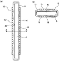
- FIG. 6 is an explanatory cross-sectional view showing an outline of the configuration of an example of an excimer lamp used as an ultraviolet light source having a wavelength of 220 nm or less, and (a) a cross-sectional view showing a cross section along the longitudinal direction of the discharge vessel; (B) It is the sectional view on the AA line in (a).
- This excimer lamp 10 includes a hollow discharge vessel 11 having a rectangular cross section in which both ends are hermetically sealed and a discharge space S is formed therein.
- As the discharge gas for example, xenon gas or a mixed gas of argon and chlorine is enclosed.
- the discharge vessel 11 is made of silica glass, for example, synthetic quartz glass, which transmits vacuum ultraviolet rays well, and has a function as a dielectric.
- a pair of grid electrodes that is, one electrode 15 functioning as a high voltage supply electrode and the other electrode 16 functioning as a ground electrode extend in a long direction.
- the discharge vessel 11 functioning as a dielectric is interposed between the pair of electrodes 15 and 16.
- Such an electrode can be formed, for example, by applying an electrode material made of metal to the discharge vessel 11 or by printing or vapor deposition.
- the ultraviolet reflection film 20 is, for example, an inner surface region corresponding to one electrode 15 functioning as a high voltage supply electrode on the long side surface of the discharge vessel 11 and a part of an inner surface region of a short side surface continuous with this region.
- the light emitting portion (aperture portion) 18 is formed by the absence of the ultraviolet reflecting film 20 in the inner surface region corresponding to the other electrode 16 that functions as the ground electrode on the long side surface of the discharge vessel 11. Is configured.
- the film thickness of the ultraviolet reflecting film 20 is preferably 10 to 100 ⁇ m, for example.
- the ultraviolet reflecting film 20 has a vacuum ultraviolet ray transmittance in which the silica particles and the alumina particles themselves have a high refractive index, a part of the vacuum ultraviolet rays reaching the silica particles or the alumina particles is reflected on the surface of the particles. And the other part is refracted and incident on the inside of the particle, and more of the light incident on the inside of the particle is transmitted (partially absorbed) and refracted when it is emitted again. It has a function of “diffuse reflection” in which such reflection and refraction occur repeatedly. Further, since the ultraviolet reflecting film 20 is composed of silica particles and alumina particles, that is, ceramics, the ultraviolet reflecting film 20 does not generate an impure gas and has a characteristic that can withstand discharge.
- silica particles constituting the ultraviolet reflective film 20 for example, silica glass made into fine powder particles can be used.
- Silica particles have a particle diameter defined as follows within a range of 0.01 to 20 ⁇ m, for example, and have a center particle diameter (peak value of number average particle diameter) of, for example, 0.1 to 10 ⁇ m. And more preferably 0.3 to 3 ⁇ m.
- the ratio of the silica particle which has a center particle diameter is 50% or more.
- the alumina particles constituting the ultraviolet reflecting film 20 have a particle diameter in the range of 0.1 to 10 ⁇ m, for example, and the center particle diameter (peak value of the number average particle diameter) is, for example, 0.1 to 3 ⁇ m. And more preferably 0.3 to 1 ⁇ m. Moreover, it is preferable that the ratio of the alumina particle which has a center particle diameter is 50% or more.
- the desmear treatment step may be finished with a part of the consumable resist layer 4 remaining, or may be finished after all of the consumable resist layer 4 has disappeared.
- the desmear treatment process is terminated with a part of the consumable resist layer 4 remaining, a part of the consumable resist layer 4 with the surface of the wiring board material 1 remaining forms the surface of the insulating layer 3. It becomes the surface layer part. Since the consumable resist layer 4 does not contain a filler, the insulating layer 3 having an appropriate surface roughness can be obtained by ashing by desmear treatment.
- the desmear process when the desmear process is terminated immediately after all of the consumable resist layer 4 disappears, the ashing of the insulating layer 3 is prevented by the desmear process. That is, since the roughness of the surface of the insulating layer 3 before the desmear treatment is maintained, the insulating layer 3 having an appropriate surface roughness can be obtained. In addition, when the desmear treatment process is continued after all of the consumable resist layer 4 disappears, the exposed insulating layer 3 is ashed. Thereby, since the roughness of the surface of the insulating layer 3 can be adjusted, the insulating layer 3 which has moderate surface roughness is obtained.
- the desmear treatment method of the present invention all or most of the consumable resist layer 4 is removed by the desmear treatment step, so that it is not necessary to perform the removal treatment of the consumable resist layer 4. It is not necessary to perform a roughening treatment on the insulating layer 3 after the treatment. Therefore, according to the desmear treatment method of the present invention, a complicated treatment process is not required, and sufficient desmear treatment can be performed on the inside of the hole 3a formed in the insulating layer 3, and an appropriate surface roughness is achieved.
- the insulating layer 3 having
- the consumable resist layer 4 may be formed on the surface of the insulating layer 3 after performing the hole forming step. Further, in the production of the wiring board material 1 on which the consumable resist layer 4 is formed, it is not essential to use the composite insulating layer forming material 6.
- the wiring substrate material 1 in which the insulating layer 3 is laminated on the conductive layer 2 is manufactured by an appropriate method, and a consumable resist layer forming coating solution is applied to the surface of the insulating layer 3 of the wiring substrate material 1.
- the consumable resist layer 4 may be formed by drying. Further, in the desmear treatment step, desmear treatment may be performed by radicals generated by plasma discharge. Further, in order to remove smear caused by the filler from the wiring board material 1, the wiring board material 1 may be subjected to physical vibration processing such as ultrasonic processing after the desmearing process is completed. .
- the present invention is not limited to these examples.
- the surface roughness Ra was measured using a “Nanoscale Hybrid Microscope VN-8010” manufactured by Keyence Corporation under the condition that the observation range was 50 ⁇ m ⁇ 38 ⁇ m.
- Example 1 Production of wiring board material A copper-clad laminate having a thickness of 0.4 mm was prepared by laminating a copper foil on one surface of an insulating substrate. A conductive layer having a required pattern was formed on one surface of the insulating substrate by subjecting the copper foil in the copper-clad laminate to photolithography and etching. An insulating film (“ABF-GX92” manufactured by Ajinomoto Fine Techno Co., Ltd.), in which an insulating layer containing a filler is laminated on a PET film as a carrier layer, is laminated on one surface of an insulating substrate including a conductive layer. Then, the PET film was peeled off.
- ABSGX92 manufactured by Ajinomoto Fine Techno Co., Ltd.
- the thickness of the insulating layer in this insulating film is 20 ⁇ m.
- Lamination was performed using a batch type vacuum pressure laminator under a pressure of 10000 hPa or less, a temperature of 110 ° C., and a pressure of 500 kN / m 2 . And the thermosetting process of the insulating layer was performed for 30 minutes at 170 degreeC. In this way, a wiring board material having an insulating layer made of an epoxy resin containing a conductive layer and a filler was produced.
- the surface roughness Ra of the insulating layer in this wiring board material was 52 nm.
- Hole formation process A hole with a diameter of 50 ⁇ m that penetrates the consumable resist layer and the insulating layer is formed by performing laser processing on the wiring board material on which the consumable resist layer is formed, using a carbon dioxide laser device. did.
- Desmear treatment process The wiring board material which passed through the hole formation process of said (3) was mounted on the stage provided with the heating means. Then, desmear treatment was performed by irradiating the wiring board material with ultraviolet rays through an ultraviolet transmission window while supplying oxygen gas. Specific conditions for the desmear treatment are as follows.
- Example 2 (1) Manufacture of composite insulating layer forming material 20 parts by mass of liquid bisphenol A type epoxy resin ("jER @ 828EL” manufactured by Mitsubishi Chemical Corporation) and epoxy resin curing agent (“jER manufactured by Mitsubishi Chemical Corporation") @Cure ST12 ”) 12 parts by mass and a diluent (“ Reactive Diluent YDE “manufactured by Mitsubishi Chemical Corporation) were mixed to prepare a consumable resist layer forming coating solution.
- This consumable resist layer forming coating solution is applied onto a base layer made of a PET film with an alkyd mold release material (AL-5) (Lintech Co., Ltd., thickness: 38 ⁇ m) using a die coater, and the coating solution is formed at 100 ° C. for 5 minutes.
- the consumable resist layer made of an epoxy resin having a thickness of 1.5 ⁇ m was formed on the base layer by drying under the conditions described above.
- This insulating layer forming coating solution is applied to the surface of the consumable resist layer with a die coater and dried at 100 ° C. for 5 minutes to form an insulating layer having a thickness of 20 ⁇ m on the consumable resist layer. did. In this way, a composite insulating layer forming material in which a consumable resist layer and an insulating layer were laminated on the base layer was manufactured.
- a copper-clad laminate in which a copper foil having a thickness of 4 mm was laminated on one surface of an insulating substrate was prepared.
- a conductive layer having a required pattern was formed on one surface of the insulating substrate by subjecting the copper foil in the copper-clad laminate to photolithography and etching.
- the composite insulating layer forming material was disposed on one surface of the insulating substrate including the conductive layer so that the insulating layer was in contact with one surface of the insulating substrate.
- an insulating substrate and a composite insulating layer forming material are laminated with a batch type vacuum pressure laminator at a pressure of 10000 hPa, a temperature of 110 ° C., and a pressure of 500 kN / m 2.
- the layer was peeled off.
- the consumable resist layer and the insulating layer were thermally cured at 170 ° C. for 30 minutes.
- a wiring board material having an insulating layer made of an epoxy resin containing a conductive layer and a filler and having a consumable resist layer formed on the insulating layer was manufactured.
- Hole formation process A hole with a diameter of 50 ⁇ m that penetrates the consumable resist layer and the insulating layer is formed by performing laser processing on the wiring board material on which the consumable resist layer is formed, using a carbon dioxide laser device. did.
- Desmear treatment process The wiring board material which passed through the hole formation process of said (3) was mounted on the stage provided with the heating means. Then, desmear treatment was performed by irradiating the wiring board material with ultraviolet rays through an ultraviolet transmission window while supplying oxygen gas (concentration: 100%). Specific conditions for the desmear treatment are as follows.
- Example 1 A wiring board material was manufactured in the same manner as in Example 1 except that the consumable resist layer was not formed, and a hole forming process, a desmearing process, and a physical vibration process were performed on the wiring board material.
Landscapes
- Engineering & Computer Science (AREA)
- Manufacturing & Machinery (AREA)
- Microelectronics & Electronic Packaging (AREA)
- Chemical & Material Sciences (AREA)
- Physics & Mathematics (AREA)
- Optics & Photonics (AREA)
- Life Sciences & Earth Sciences (AREA)
- Materials Engineering (AREA)
- Wood Science & Technology (AREA)
- Organic Chemistry (AREA)
- Printing Elements For Providing Electric Connections Between Printed Circuits (AREA)
- Manufacturing Of Printed Wiring (AREA)
Abstract
本発明は、複雑な工程が不要で、絶縁層に形成された貫通孔の内部に対して十分なデスミア処理を行うことができると共に、適度な表面粗度を有する絶縁層が得られる配線基板材料のデスミア処理方法、このデスミア処理方法に供される配線基板材料の製造方法、およびこの製造方法に用いられる複合絶縁層形成材料を提供することを目的とする。 本発明のデスミア処理方法は、導電層上にフィラーが含有された樹脂よりなる絶縁層が積層されてなる配線基板材料のデスミア処理方法であって、絶縁層を厚み方向に貫通するホールを形成するホール形成工程と、このホール形成工程を経由した配線基板材料をラジカルによって処理するデスミア処理工程とを有し、デスミア処理工程に供される配線基板材料には、当該絶縁層上に消耗性レジスト層が形成されており、この消耗性レジスト層は、デスミア処理工程において消耗される樹脂よりなることを特徴とする。
Description
本発明は、導電層上にフィラーが含有された樹脂よりなる絶縁層が積層されてなる配線基板材料のデスミア処理方法、このデスミア処理方法に供される配線基板材料の製造方法、並びに上記のデスミア処理方法または上記の製造方法に用いられる複合絶縁層形成材料に関する。
例えば半導体集積回路素子等の半導体素子を搭載するための配線基板としては、絶縁層と導電層(配線層)とが交互に積層されてなる多層配線基板が知られている。このような多層配線基板においては、一の導電層と他の導電層とを電気的に接続するため、1つの若しくは複数の絶縁層を厚み方向に貫通して伸びるビアホールやスルーホールが形成されている。
多層配線基板の製造工程においては、絶縁層と導電層とが積層されてなる配線基板材料に、ドリル加工やレーザ加工を施すことによって絶縁層の一部を除去することにより、ビアホールやスルーホールなどの貫通孔が形成される。そして、絶縁層に貫通孔を形成する際には、配線基板材料には絶縁層を構成する材料に起因するスミア(残渣)が生じる。このため、当該配線基板材料に対してスミアを除去するデスミア処理が行われる。
多層配線基板の製造工程においては、絶縁層と導電層とが積層されてなる配線基板材料に、ドリル加工やレーザ加工を施すことによって絶縁層の一部を除去することにより、ビアホールやスルーホールなどの貫通孔が形成される。そして、絶縁層に貫通孔を形成する際には、配線基板材料には絶縁層を構成する材料に起因するスミア(残渣)が生じる。このため、当該配線基板材料に対してスミアを除去するデスミア処理が行われる。
このデスミア処理としては、従来、過マンガン酸カリウムや水酸化ナトリウムが溶解されてなるアルカリ溶液によって処理する湿式処理方法や、紫外線および当該紫外線により生ずるオゾンや酸素ラジカルによって処理する乾式処理方法が知られている。このようなデスミア処理方法においては、ビアホールやスルーホールの内部に付着したスミアが除去されると共に、絶縁層の表面の粗面化が行われる。
しかしながら、上記のデスミア処理方法において、スミアが十分に除去される条件でデスミア処理を行った場合には、絶縁層の表面が過度に粗面化されてしまう。これは、絶縁層を構成する樹脂が過度に分解されることによって、絶縁層中に含有されたフィラーが当該絶縁層の表面に露出するからである。このため、絶縁層上に形成される導電層のライン・アンド・スペースが、例えばそれぞれ15μm以下である場合には、配線倒れが生じたり、高周波の信号応答性の低下が生じたりする、という問題がある。
しかしながら、上記のデスミア処理方法において、スミアが十分に除去される条件でデスミア処理を行った場合には、絶縁層の表面が過度に粗面化されてしまう。これは、絶縁層を構成する樹脂が過度に分解されることによって、絶縁層中に含有されたフィラーが当該絶縁層の表面に露出するからである。このため、絶縁層上に形成される導電層のライン・アンド・スペースが、例えばそれぞれ15μm以下である場合には、配線倒れが生じたり、高周波の信号応答性の低下が生じたりする、という問題がある。
このような問題を解決するため、絶縁層の表面に保護層を形成した状態で、保護層および絶縁層を貫通する貫通孔を形成し、その後、貫通孔の内面をデスミア処理する方法が提案されている(特許文献1および特許文献2参照。)。
しかしながら、このような方法においては、デスミア処理を行った後に、保護層を除去することが必要となる。また、絶縁層の表面の粗度が小さすぎる場合には、更に、絶縁層の表面を粗面化処理することが必要となる。このため、処理工程全体が複雑となる、という問題がある。
しかしながら、このような方法においては、デスミア処理を行った後に、保護層を除去することが必要となる。また、絶縁層の表面の粗度が小さすぎる場合には、更に、絶縁層の表面を粗面化処理することが必要となる。このため、処理工程全体が複雑となる、という問題がある。
本発明は、以上のような事情に基づいてなされたものであって、その目的は、複雑な処理工程が不要で、絶縁層に形成されたホールの内部に対して十分なデスミア処理を行うことができると共に、適度な表面粗度を有する絶縁層が得られる配線基板材料のデスミア処理方法を提供することにある。
本発明の他の目的は、上記のデスミア処理方法に供される配線基板材料の製造方法、お並びに上記のデスミア処理方法または上記の製造方法に用いられる複合絶縁層形成材料を提供することにある。
本発明の他の目的は、上記のデスミア処理方法に供される配線基板材料の製造方法、お並びに上記のデスミア処理方法または上記の製造方法に用いられる複合絶縁層形成材料を提供することにある。
本発明の配線基板材料のデスミア処理方法は、導電層上にフィラーが含有された樹脂よりなる絶縁層が積層されてなる配線基板材料のデスミア処理方法であって、
前記絶縁層を厚み方向に貫通するホールを形成するホール形成工程と、このホール形成工程を経由した配線基板材料をラジカルによって処理するデスミア処理工程とを有し、
前記デスミア処理工程に供される前記配線基板材料には、当該絶縁層上に消耗性レジスト層が形成されており、この消耗性レジスト層は、前記デスミア処理工程において消耗される樹脂よりなることを特徴とする。
前記絶縁層を厚み方向に貫通するホールを形成するホール形成工程と、このホール形成工程を経由した配線基板材料をラジカルによって処理するデスミア処理工程とを有し、
前記デスミア処理工程に供される前記配線基板材料には、当該絶縁層上に消耗性レジスト層が形成されており、この消耗性レジスト層は、前記デスミア処理工程において消耗される樹脂よりなることを特徴とする。
本発明の配線基板材料のデスミア処理方法においては、前記ホール形成工程に供される前記配線基板材料には、当該絶縁層上に前記消耗性レジスト層が形成されていることが好ましい。
また、前記デスミア処理工程は、ラジカル源を含む雰囲気下において、前記波長220nm以下の紫外線を前記消耗性レジスト層の上方から前記ホールの底部に向かって照射することによって行われることが好ましい。
また、前記消耗性レジスト層の厚みが0.05~5μmであることが好ましい。
また、前記消耗性レジスト層は、前記絶縁層を構成する樹脂と同質の樹脂よりなり、
前記デスミア処理工程は、前記消耗性レジスト層の一部が残存した状態で終了してもよい。
また、前記デスミア処理工程は、前記消耗性レジスト層の全部が消失した後に終了してもよい。
また、前記デスミア処理工程は、ラジカル源を含む雰囲気下において、前記波長220nm以下の紫外線を前記消耗性レジスト層の上方から前記ホールの底部に向かって照射することによって行われることが好ましい。
また、前記消耗性レジスト層の厚みが0.05~5μmであることが好ましい。
また、前記消耗性レジスト層は、前記絶縁層を構成する樹脂と同質の樹脂よりなり、
前記デスミア処理工程は、前記消耗性レジスト層の一部が残存した状態で終了してもよい。
また、前記デスミア処理工程は、前記消耗性レジスト層の全部が消失した後に終了してもよい。
本発明の配線基板材料の製造方法は、上記のデスミア処理方法に供される配線基板材料の製造方法であって、
ベース層上に、前記消耗性レジスト層を介して前記絶縁層が形成された積層体よりなる複合絶縁層形成用材料を、前記導電層上に前記絶縁層が接するよう積層し、その後、前記ベース層を除去することを特徴とする。
ベース層上に、前記消耗性レジスト層を介して前記絶縁層が形成された積層体よりなる複合絶縁層形成用材料を、前記導電層上に前記絶縁層が接するよう積層し、その後、前記ベース層を除去することを特徴とする。
本発明の複合絶縁層形成材料は、ベース層上に、前記消耗性レジスト層を介して前記絶縁層が形成された積層体よりなり、上記の配線基板材料の製造方法に用いられることを特徴とする。
また、本発明の複合絶縁層形成材料は、ベース層上に、前記消耗性レジスト層を介して前記絶縁層が形成された積層体よりなり、上記のデスミア処理方法に供される配線基板材料を製造するために用いられることを特徴とする。
本発明のデスミア処理方法によれば、複雑な処理工程が不要で、絶縁層に形成されたホールの内部に対して十分なデスミア処理を行うことができると共に、適度な表面粗度を有する絶縁層が得られる。
以下、本発明の実施の形態について説明する。
図1は、本発明のデスミア処理方法における処理対象となる配線基板材料の一例における要部の構成を示す説明用断面図である。この配線基板材料1は、金属よりなる導電層2上に、フィラーが含有された樹脂よりなる絶縁層3が積層された積層体によって構成されている。
図1は、本発明のデスミア処理方法における処理対象となる配線基板材料の一例における要部の構成を示す説明用断面図である。この配線基板材料1は、金属よりなる導電層2上に、フィラーが含有された樹脂よりなる絶縁層3が積層された積層体によって構成されている。
導電層2を構成する金属としては、銅、ニッケル、金などを用いることができる。
また、導電層2の厚みは、例えば10~100μmである。
また、導電層2の厚みは、例えば10~100μmである。
絶縁層3を構成する樹脂としては、エポキシ樹脂、ビスマレイミドトリアジン樹脂、ポリイミド樹脂、ポリエステル樹脂などを用いることができる。
絶縁層3中に含有されるフィラーを構成する材料としては、シリカ、アルミナ、マイカ、珪酸塩、硫酸バリウム、水酸化マグネシウム、酸化チタンなどを用いることができる。このフィラーの平均粒子径は、例えば0.1~3μmである。
また、絶縁層3におけるフィラーの含有割合は、例えば20~60質量%である。
絶縁層3中に含有されるフィラーを構成する材料としては、シリカ、アルミナ、マイカ、珪酸塩、硫酸バリウム、水酸化マグネシウム、酸化チタンなどを用いることができる。このフィラーの平均粒子径は、例えば0.1~3μmである。
また、絶縁層3におけるフィラーの含有割合は、例えば20~60質量%である。
本発明のデスミア処理方法においては、上記の配線基板材料1における絶縁層を厚み方向に貫通するホールを形成するホール形成工程と、このホール形成工程を経由した配線基板材料1をラジカルによって処理するデスミア処理工程とを行う。
ホール形成工程に供される配線基板材料1には、図2に示すように、絶縁層3上に消耗性レジスト層4が形成されていることが好ましい。この消耗性レシスト層4は、後続のデスミア処理工程において、ラジカルが接触することによって消耗され得る樹脂により構成されている。
消耗性レジスト層4を構成する樹脂としては、アクリル樹脂、ウレタン樹脂、エポキシ樹脂、フタル酸樹脂、ビニル樹脂などを用いることができる。
後述するデスミア処理工程を消耗性レジスト層4の全部が消失した後に終了する場合には、消耗性レジスト層4を構成する樹脂として熱可塑性樹脂を用いることが好ましい。熱硬化性樹脂を用いる場合には、後述するデスミア処理工程において消耗性レジスト層4を除去することが困難となることがある。
また、後述するデスミア処理工程を消耗性レジスト層4の一部が残存した状態で終了する場合には、消耗性レジスト層4を構成する樹脂として絶縁層3を構成する樹脂と同質の樹脂を用いることが好ましい。
消耗性レジスト層4を構成する樹脂としては、アクリル樹脂、ウレタン樹脂、エポキシ樹脂、フタル酸樹脂、ビニル樹脂などを用いることができる。
後述するデスミア処理工程を消耗性レジスト層4の全部が消失した後に終了する場合には、消耗性レジスト層4を構成する樹脂として熱可塑性樹脂を用いることが好ましい。熱硬化性樹脂を用いる場合には、後述するデスミア処理工程において消耗性レジスト層4を除去することが困難となることがある。
また、後述するデスミア処理工程を消耗性レジスト層4の一部が残存した状態で終了する場合には、消耗性レジスト層4を構成する樹脂として絶縁層3を構成する樹脂と同質の樹脂を用いることが好ましい。
消耗性レジスト層4の厚みは、0.05~5μmであることが好ましい。この厚みが0.05μm未満である場合には、スミアが十分に除去される前に消耗性レジスト層4の全部が消失する。そのため、露出した絶縁層3がアッシングされる。これにより、絶縁層3の表面にフィラーが露出する。その結果、絶縁層3の表面が過度に粗面化される。一方、この厚みが5μmを超える場合には、形成されるホールに対する消耗性レジスト層4の厚みが大きくなる、すなわち、アスペクト比が大きくなるので、デスミア処理のスピード自体が遅くなるという、問題が発生する。具体的に説明すると、配線基板材料1に照射される紫外線が平行光であれば、ホールの開口とホールの底部との光量比は1:1になる。しかし、配線基板材料1に照射される紫外線が平行光でない場合には、ホールの底部に到達する光量は低下するため、ホールの開口とホールの底部との光量比は例えば1:0.2である。従って、消耗性レジスト層4の厚みは、スミアの厚みの1 ~5倍でよいことがわかる。そして、スミアの厚みは、一般的には0.05~1μm程度であるため、消耗性レジスト層4の厚みは0.05~5μmであることが好ましい。実際の消耗性レジスト層4の厚みは、デスミア処理によってホールの底部のスミアが十分に除去されるまでの時間および消耗性レジスト層4がアッシングされる速度などを考慮して設定すればよい。
このような消耗性レジスト層4が形成された配線基板材料1は、以下のようにして製造することができる。
先ず、図3に示すように、ベース層5上に、消耗性レジスト層4を介して絶縁層3が形成された積層体よりなる複合絶縁層形成用材料6を製造する。
次いで、図4に示すように、複合絶縁層形成用材料6を、例えば絶縁性基板(図示省略)の表面に形成された導電層2上に絶縁層3が接するよう積層して接着する。その後、ベース層5を消耗性レジスト層4から除去する。これにより、消耗性レジスト層4が形成された配線基板材料1が得られる。
先ず、図3に示すように、ベース層5上に、消耗性レジスト層4を介して絶縁層3が形成された積層体よりなる複合絶縁層形成用材料6を製造する。
次いで、図4に示すように、複合絶縁層形成用材料6を、例えば絶縁性基板(図示省略)の表面に形成された導電層2上に絶縁層3が接するよう積層して接着する。その後、ベース層5を消耗性レジスト層4から除去する。これにより、消耗性レジスト層4が形成された配線基板材料1が得られる。
以上において、ベース層5を構成する材料としては、PETフィルム、ポリエチレンフィルム、ポリプロピレンフィルム、ポリカーバイトフィルムなどを用いることができる。また、ベース層5の厚みは、例えば10~~200μmである。
複合絶縁層形成用材料6は、例えば以下のようにして製造することができる。
先ず、適宜の溶媒中に消耗性レジスト層4を構成する樹脂材料が含有されてなる消耗性レジスト層形成用塗布液、および適宜の溶媒中に絶縁層3を構成する樹脂材料およびフィラーが含有されてなる絶縁層形成用塗布液を調製する。次いで、離型材によって処理されたベース層5の表面に消耗性レジスト層形成用塗布液を塗布して乾燥することにより、消耗性レジスト層4を形成する。そして、消耗性レジスト層4の表面に絶縁層形成用塗布液を塗布して乾燥することにより、絶縁層3を形成する。このようにして、複合絶縁層形成用材料6を製造することができる。
以上において、消耗性レジスト層形成用塗布液および絶縁層形成用塗布液を塗布する手段としては、ダイコータを用いることができる。
先ず、適宜の溶媒中に消耗性レジスト層4を構成する樹脂材料が含有されてなる消耗性レジスト層形成用塗布液、および適宜の溶媒中に絶縁層3を構成する樹脂材料およびフィラーが含有されてなる絶縁層形成用塗布液を調製する。次いで、離型材によって処理されたベース層5の表面に消耗性レジスト層形成用塗布液を塗布して乾燥することにより、消耗性レジスト層4を形成する。そして、消耗性レジスト層4の表面に絶縁層形成用塗布液を塗布して乾燥することにより、絶縁層3を形成する。このようにして、複合絶縁層形成用材料6を製造することができる。
以上において、消耗性レジスト層形成用塗布液および絶縁層形成用塗布液を塗布する手段としては、ダイコータを用いることができる。
絶縁層3を導電層2に接着する方法としては、熱圧着などによる方法などを利用することができる。
また、ベース層5は、消耗性レジスト層4から剥離されることによって除去される。
また、ベース層5は、消耗性レジスト層4から剥離されることによって除去される。
そして、ホール形成工程においては、図5に示すように、消耗性レジスト層4を厚み方向に貫通するホール4aを形成すると共に、このホール4aに連通する、絶縁層3を厚み方向に貫通するホール3aを形成する。
絶縁層3および消耗性レジスト層4にホール3a,4aを形成する方法としては、ドリル加工による方法、レーザ加工による方法を利用することができる。レーザ加工によってホール3a,4aを形成する場合には、炭酸ガスレーザ装置やYAGレーザ装置などを用いることができる。
絶縁層3におけるホール3aの径に対する絶縁層3および消耗性レジスト層4の厚みの合計の比は、2.5以下であることが好ましく、より好ましくは2以下である。この比が2.5を超える場合には、デスミア処理のスピード自体が遅くなる、という問題が発生する。
このようにして得られる配線基板材料1においては、絶縁層3におけるホール3aの内壁面、およびホール3aの底部すなわち導電層2におけるホール3aによって露出した部分などには、ホール3aを形成する際に生じたスミアが残留している。
デスミア処理工程においては、絶縁層3に形成されたホール3aの内面および底面がラジカルによってデスミア処理される。また、デスミア処理工程においては、消耗性レジスト層4がラジカルによって消耗される。
このデスミア処理工程における具体的な処理方法としては、ラジカル源を含む雰囲気下において、波長220nm以下の紫外線を消耗性レジスト層4の上方から絶縁層3のホール3aの底部に向かって照射する方法を挙げることができる。
このデスミア処理工程における具体的な処理方法としては、ラジカル源を含む雰囲気下において、波長220nm以下の紫外線を消耗性レジスト層4の上方から絶縁層3のホール3aの底部に向かって照射する方法を挙げることができる。
このようなデスミア処理工程において、ラジカル源としては、220nm以下の紫外線が照射されることによってラジカルを生成するものが用いられる。ラジカル源の具体例としては、酸素ガス、オゾン等の酸素ラジカルを生成するもの、水蒸気等のOHラジカルを生成するものなどが挙げられる。
また、雰囲気ガス中におけるラジカル源の濃度は、ラジカル源の種類によって適宜選択される。例えばラジカル源が酸素ガスである場合には、酸素ガスの濃度は50~100%であることが好ましい。
また、雰囲気ガス中におけるラジカル源の濃度は、ラジカル源の種類によって適宜選択される。例えばラジカル源が酸素ガスである場合には、酸素ガスの濃度は50~100%であることが好ましい。
配線基板材料1に照射される紫外線は、波長220nm以下、好ましくは190nm以下とされる。紫外線の波長が220nmを超える場合には、スミアや消耗性レジスト層4を除去することが困難となる。
波長220nm以下の紫外線の光源としては、キセノンエキシマランプ(ピーク波長172nm)、低圧水銀灯(185nm輝線)、希ガス蛍光ランプなどを用いることができる。
配線基板材料1に照射される紫外線の照度は、例えば10~1000mW/cm2 である。また、配線基板材料1に対する紫外線の照射時間は、紫外線の照度やスミアの残留状態などを考慮して適宜設定されるが、例えば1~180分間である。
波長220nm以下の紫外線の光源としては、キセノンエキシマランプ(ピーク波長172nm)、低圧水銀灯(185nm輝線)、希ガス蛍光ランプなどを用いることができる。
配線基板材料1に照射される紫外線の照度は、例えば10~1000mW/cm2 である。また、配線基板材料1に対する紫外線の照射時間は、紫外線の照度やスミアの残留状態などを考慮して適宜設定されるが、例えば1~180分間である。
図6は、波長220nm以下の紫外線の光源として用いられるエキシマランプの一例における構成の概略を示す説明用断面図であって、(a)放電容器の長手方向に沿った断面を示す横断面図、(b)(a)におけるA-A線断面図である。
このエキシマランプ10は、両端が気密に封止されて内部に放電空間Sが形成された、断面矩形状の中空長尺状の放電容器11を備えており、この放電容器11の内部には、放電用ガスとして、例えばキセノンガスや、アルゴンと塩素とを混合したガスが封入されている。
放電容器11は、真空紫外線を良好に透過するシリカガラス、例えば合成石英ガラスよりなり、誘電体としての機能を有する。
このエキシマランプ10は、両端が気密に封止されて内部に放電空間Sが形成された、断面矩形状の中空長尺状の放電容器11を備えており、この放電容器11の内部には、放電用ガスとして、例えばキセノンガスや、アルゴンと塩素とを混合したガスが封入されている。
放電容器11は、真空紫外線を良好に透過するシリカガラス、例えば合成石英ガラスよりなり、誘電体としての機能を有する。
放電容器11における長辺面の外表面には、一対の格子状の電極、すなわち、高電圧供給電極として機能する一方の電極15および接地電極として機能する他方の電極16が長尺な方向に伸びるよう対向して配置されており、これにより、一対の電極15,16間に誘電体として機能する放電容器11が介在された状態とされている。
このような電極は、例えば、金属よりなる電極材料を放電容器11にペースト塗布することにより、あるいは、プリント印刷や蒸着することによって形成することができる。
このような電極は、例えば、金属よりなる電極材料を放電容器11にペースト塗布することにより、あるいは、プリント印刷や蒸着することによって形成することができる。
このエキシマランプ10においては、一方の電極15に点灯電力が供給されると、誘電体として機能する放電容器11の壁を介して両電極15,16間に放電が生成され、これにより、エキシマ分子が形成されると共にこのエキシマ分子から真空紫外線が放射されるエキシマ放電が生ずるが、このエキシマ放電によって発生する真空紫外線を効率良く利用するために、放電容器11の内表面に、シリカ粒子とアルミナ粒子とからなる紫外線反射膜20が設けられている。ここに、放電用ガスとしてキセノンガスを用いた場合は、波長172nmにピークを有する真空紫外線が放出され、放電用ガスとしてアルゴンと塩素とを混合したガスを用いた場合には、波長175nmにピークを有する真空紫外線が放出される。
紫外線反射膜20は、例えば、放電容器11における長辺面の、高電圧供給電極として機能する一方の電極15に対応する内表面領域とこの領域に連続する短辺面の内表面領域の一部にわたって形成されており、放電容器11における長辺面の、接地電極として機能する他方の電極16に対応する内表面領域において紫外線反射膜20が形成されていないことによって光出射部(アパーチャ部)18が構成されている。
紫外線反射膜20の膜厚は、例えば10~100μmであることが好ましい。
紫外線反射膜20の膜厚は、例えば10~100μmであることが好ましい。
紫外線反射膜20は、シリカ粒子およびアルミナ粒子それ自体が高い屈折率を有する真空紫外線透過性を有するものであることから、シリカ粒子またはアルミナ粒子に到達した真空紫外線の一部が粒子の表面で反射されると共に他の一部が屈折して粒子の内部に入射され、さらに、粒子の内部に入射される光の多くが透過され(一部が吸収)、再び、出射されるに際して屈折される、このような反射、屈折が繰り返し起こる「拡散反射」させる機能を有する。
また、紫外線反射膜20は、シリカ粒子およびアルミナ粒子、すなわちセラミックスにより構成されていることにより、不純ガスを発生させず、また、放電に耐えられる特性を有する。
また、紫外線反射膜20は、シリカ粒子およびアルミナ粒子、すなわちセラミックスにより構成されていることにより、不純ガスを発生させず、また、放電に耐えられる特性を有する。
紫外線反射膜20を構成するシリカ粒子は、例えばシリカガラスを粉末状に細かい粒子としたものなどを用いることができる。
シリカ粒子は、以下のように定義される粒子径が例えば0.01~20μmの範囲内にあるものであって、中心粒径(数平均粒子径のピーク値)が、例えば0.1~10μmであるものが好ましく、より好ましくは0.3~3μmであるものである。
また、中心粒径を有するシリカ粒子の割合が50%以上であることが好ましい。
シリカ粒子は、以下のように定義される粒子径が例えば0.01~20μmの範囲内にあるものであって、中心粒径(数平均粒子径のピーク値)が、例えば0.1~10μmであるものが好ましく、より好ましくは0.3~3μmであるものである。
また、中心粒径を有するシリカ粒子の割合が50%以上であることが好ましい。
紫外線反射膜20を構成するアルミナ粒子は、粒子径が例えば0.1~10μmの範囲内にあるものであって、中心粒径(数平均粒子径のピーク値)が、例えば0.1~3μmであるものが好ましく、より好ましくは0.3~1μmであるものである。
また、中心粒径を有するアルミナ粒子の割合が50%以上であることが好ましい。
また、中心粒径を有するアルミナ粒子の割合が50%以上であることが好ましい。
本発明のデスミア処理方法においては、デスミア処理工程は、消耗性レジスト層4の一部が残存した状態で終了してもよく、消耗性レジスト層4の全部が消失した後に終了してもよい。
消耗性レジスト層4の一部が残存した状態でデスミア処理工程を終了させた場合には、配線基板材料1の表面が残存した消耗性レジスト層4の一部が絶縁層3の表面を形成する表層部分となる。そして、消耗性レジスト層4には、フィラーが含有されていないため、デスミア処理によってアッシングされることにより、適度な表面粗度を有する絶縁層3が得られる。
また、消耗性レジスト層4の全部が消失した直後にデスミア処理工程を終了させた場合には、デスミア処理によって絶縁層3がアッシングされることが防止される。すなわち、デスミア処理前における絶縁層3の表面の粗度が維持されるので、適度な表面粗度を有する絶縁層3が得られる。
また、消耗性レジスト層4の全部が消失した後にデスミア処理工程を続行させた場合には、露出した絶縁層3がアッシングされる。これにより、絶縁層3の表面の粗度を調整することができるので、適度な表面粗度を有する絶縁層3が得られる。
また、本発明のデスミア処理方法においては、デスミア処理工程によって消耗性レジスト層4の全部若しくは大部分が除去されるので、消耗性レジスト層4の除去処理を行うことが不要であり、また、デスミア処理後に、絶縁層3の粗面化処理を行うことが不要である。
従って、本発明のデスミア処理方法によれば、複雑な処理工程が不要で、絶縁層3に形成されたホール3aの内部に対して十分なデスミア処理を行うことができると共に、適度な表面粗度を有する絶縁層3が得られる。
消耗性レジスト層4の一部が残存した状態でデスミア処理工程を終了させた場合には、配線基板材料1の表面が残存した消耗性レジスト層4の一部が絶縁層3の表面を形成する表層部分となる。そして、消耗性レジスト層4には、フィラーが含有されていないため、デスミア処理によってアッシングされることにより、適度な表面粗度を有する絶縁層3が得られる。
また、消耗性レジスト層4の全部が消失した直後にデスミア処理工程を終了させた場合には、デスミア処理によって絶縁層3がアッシングされることが防止される。すなわち、デスミア処理前における絶縁層3の表面の粗度が維持されるので、適度な表面粗度を有する絶縁層3が得られる。
また、消耗性レジスト層4の全部が消失した後にデスミア処理工程を続行させた場合には、露出した絶縁層3がアッシングされる。これにより、絶縁層3の表面の粗度を調整することができるので、適度な表面粗度を有する絶縁層3が得られる。
また、本発明のデスミア処理方法においては、デスミア処理工程によって消耗性レジスト層4の全部若しくは大部分が除去されるので、消耗性レジスト層4の除去処理を行うことが不要であり、また、デスミア処理後に、絶縁層3の粗面化処理を行うことが不要である。
従って、本発明のデスミア処理方法によれば、複雑な処理工程が不要で、絶縁層3に形成されたホール3aの内部に対して十分なデスミア処理を行うことができると共に、適度な表面粗度を有する絶縁層3が得られる。
本発明は、上記の実施の形態に限定されず、以下のような変更を加えることができる。
例えば消耗性レジスト層4は、ホール形成工程を行った後に、絶縁層3の表面に形成してもよい。
また、消耗性レジスト層4が形成された配線基板材料1の製造において、複合絶縁層形成用材料6を用いることは必須ではない。例えば適宜の方法によって導電層2上に絶縁層3が積層されてなる配線基板材料1を製造し、この配線基板材料1の絶縁層3の表面に、消耗性レジスト層形成用塗布液を塗布して乾燥することによって、消耗性レジスト層4を形成してもよい。
また、デスミア処理工程においては、プラズマ放電によるラジカルによってデスミア処理してもよい。
また、フィラーに起因するスミアを配線基板材料1から離脱させるために、当該配線基板材料1に対して、デスミア処理工程が終了した後に、例えば超音波処理などの物理的振動処理を施してもよい。
例えば消耗性レジスト層4は、ホール形成工程を行った後に、絶縁層3の表面に形成してもよい。
また、消耗性レジスト層4が形成された配線基板材料1の製造において、複合絶縁層形成用材料6を用いることは必須ではない。例えば適宜の方法によって導電層2上に絶縁層3が積層されてなる配線基板材料1を製造し、この配線基板材料1の絶縁層3の表面に、消耗性レジスト層形成用塗布液を塗布して乾燥することによって、消耗性レジスト層4を形成してもよい。
また、デスミア処理工程においては、プラズマ放電によるラジカルによってデスミア処理してもよい。
また、フィラーに起因するスミアを配線基板材料1から離脱させるために、当該配線基板材料1に対して、デスミア処理工程が終了した後に、例えば超音波処理などの物理的振動処理を施してもよい。
以下、本発明の具体的な実施例について説明するが、本発明はこれらの実施例に限定されるものではない。
また、以下の実施例において、表面粗さRaは、キーエンス社製の「ナノスケールハイブリッド顕微鏡 VN-8010」を用い、観察範囲が50μm×38μmの条件で測定した。
また、以下の実施例において、表面粗さRaは、キーエンス社製の「ナノスケールハイブリッド顕微鏡 VN-8010」を用い、観察範囲が50μm×38μmの条件で測定した。
〈実施例1〉
(1)配線基板材料の製造
絶縁性基板の一面に銅箔が積層されて厚みが0.4mmとなる銅張積層板を用意した。この銅張積層板における銅箔に対して、フォトリソグラフィーおよびエッチング処理を施すことにより、絶縁性基板の一面に所要のパターンの導電層を形成した。
導電層を含む絶縁性基板の一面に、キャリア層であるPETフィルム上にフィラーが含有された絶縁層が積層されてなる絶縁フィルム(味の素ファインテクノ(株)製の「ABF-GX92」)をラミネートし、その後、PETフィルムを剥離した。この絶縁フィルムにおける絶縁層の厚みは20μmである。ラミネートは、バッチ式真空加圧ラミネーターを用い、10000hPa以下の気圧下で、温度が110℃、圧力が500kN/m2 の条件で行った。そして、170℃で30分間で、絶縁層の熱硬化処理を行った。
このようにして、導電層およびフィラーが含有されたエポキシ樹脂よりなる絶縁層を有する配線基板材料を製造した。この配線基板材料における絶縁層の表面粗さRaは、52nmであった。
(1)配線基板材料の製造
絶縁性基板の一面に銅箔が積層されて厚みが0.4mmとなる銅張積層板を用意した。この銅張積層板における銅箔に対して、フォトリソグラフィーおよびエッチング処理を施すことにより、絶縁性基板の一面に所要のパターンの導電層を形成した。
導電層を含む絶縁性基板の一面に、キャリア層であるPETフィルム上にフィラーが含有された絶縁層が積層されてなる絶縁フィルム(味の素ファインテクノ(株)製の「ABF-GX92」)をラミネートし、その後、PETフィルムを剥離した。この絶縁フィルムにおける絶縁層の厚みは20μmである。ラミネートは、バッチ式真空加圧ラミネーターを用い、10000hPa以下の気圧下で、温度が110℃、圧力が500kN/m2 の条件で行った。そして、170℃で30分間で、絶縁層の熱硬化処理を行った。
このようにして、導電層およびフィラーが含有されたエポキシ樹脂よりなる絶縁層を有する配線基板材料を製造した。この配線基板材料における絶縁層の表面粗さRaは、52nmであった。
(2)消耗性レジスト層の形成
配線基板材料における絶縁層の表面に、塗装用のアクリルラッカー((株)GISクレオス製の「Mr.COLOR 46(透明)」)を、スピンコーターによって、回転数が5000rpm、回転時間が2分間の条件で塗布した。この塗布膜を、室温で10分間乾燥することにより、絶縁層の表面に、厚みが2μmのアクリル樹脂よりなる消耗性レジスト層を形成した。
配線基板材料における絶縁層の表面に、塗装用のアクリルラッカー((株)GISクレオス製の「Mr.COLOR 46(透明)」)を、スピンコーターによって、回転数が5000rpm、回転時間が2分間の条件で塗布した。この塗布膜を、室温で10分間乾燥することにより、絶縁層の表面に、厚みが2μmのアクリル樹脂よりなる消耗性レジスト層を形成した。
(3)ホール形成工程
消耗性レジスト層が形成された配線基板材料に対して、炭酸ガスレーザ装置によってレーザ加工を施すことにより、消耗性レジスト層および絶縁層を貫通する、径が50μmのホールを形成した。
消耗性レジスト層が形成された配線基板材料に対して、炭酸ガスレーザ装置によってレーザ加工を施すことにより、消耗性レジスト層および絶縁層を貫通する、径が50μmのホールを形成した。
(4)デスミア処理工程
上記(3)のホール形成工程を経由した配線基板材料を加熱手段を備えたステージ上に載置した。そして、配線基板材料に対して、酸素ガスを供給しながら、紫外線透過窓を介して紫外線を照射することにより、デスミア処理を行った。デスミア処理の具体的な条件は下記の通りである。
紫外線光源:キセノンエキシマランプ,有効発光長=300mm、本数=1本
紫外線透過窓の外面における紫外線照度=100W/cm2
紫外線透過窓と消耗性レジスト層との離間距離=0.5mm
紫外線照射時間=5分間
酸素ガスの流量=1L/min
ステージの温度:120℃
デスミア処理工程が終了した後、配線基板材料を調べたところ、消耗性レジスト層の全部が消失していることが確認された。
上記(3)のホール形成工程を経由した配線基板材料を加熱手段を備えたステージ上に載置した。そして、配線基板材料に対して、酸素ガスを供給しながら、紫外線透過窓を介して紫外線を照射することにより、デスミア処理を行った。デスミア処理の具体的な条件は下記の通りである。
紫外線光源:キセノンエキシマランプ,有効発光長=300mm、本数=1本
紫外線透過窓の外面における紫外線照度=100W/cm2
紫外線透過窓と消耗性レジスト層との離間距離=0.5mm
紫外線照射時間=5分間
酸素ガスの流量=1L/min
ステージの温度:120℃
デスミア処理工程が終了した後、配線基板材料を調べたところ、消耗性レジスト層の全部が消失していることが確認された。
(5)物理的振動処理
上記(4)のデスミア処理工程を経由した配線基板材料に対して、水中において下記の条件で物理的振動処理を行った。
振動板:寸法=400mm×320mm
振動板の表面から水面までの距離:130mm
配線基板材料の表面から水面までの距離:20mm
電力密度:48W/L(100%)
周波数:25kHz
処理時間:30秒間
上記(4)のデスミア処理工程を経由した配線基板材料に対して、水中において下記の条件で物理的振動処理を行った。
振動板:寸法=400mm×320mm
振動板の表面から水面までの距離:130mm
配線基板材料の表面から水面までの距離:20mm
電力密度:48W/L(100%)
周波数:25kHz
処理時間:30秒間
〈実施例2〉
(1)複合絶縁層形成用材料の製造
液状ビスフェノールA型エポキシ樹脂(三菱化学(株)製の「jER@ 828EL」)20質量部と、エポキシ樹脂硬化剤(三菱化学(株)製の「jER@キュア ST12」)12質量部と、希釈材(三菱化学(株)製の「反応性希釈材 YDE」)とを混合することにより、消耗性レジスト層形成用塗布液を調製した。
この消耗性レジスト層形成用塗布液を、ダイコータによって、アリキッド型離型材(AL-5)付きPETフィルム(リンテック(株)製,厚み38μm)よりなるベース層上に塗布し、100℃で5分間の条件で乾燥処理することにより、ベース層上に厚みが1.5μmのエポキシ樹脂よりなる消耗性レジスト層を形成した。
(1)複合絶縁層形成用材料の製造
液状ビスフェノールA型エポキシ樹脂(三菱化学(株)製の「jER@ 828EL」)20質量部と、エポキシ樹脂硬化剤(三菱化学(株)製の「jER@キュア ST12」)12質量部と、希釈材(三菱化学(株)製の「反応性希釈材 YDE」)とを混合することにより、消耗性レジスト層形成用塗布液を調製した。
この消耗性レジスト層形成用塗布液を、ダイコータによって、アリキッド型離型材(AL-5)付きPETフィルム(リンテック(株)製,厚み38μm)よりなるベース層上に塗布し、100℃で5分間の条件で乾燥処理することにより、ベース層上に厚みが1.5μmのエポキシ樹脂よりなる消耗性レジスト層を形成した。
次いで、液状ビスフェノールA型エポキシ樹脂(三菱化学(株)製の「jER@ 828EL」)28質量部と、ナフタレン型4官能エポキシ樹脂(大日本インキ化学工業(株)製の「HP4700」)28質量部と、フェノキシ樹脂(三菱化学(株)製の「YX6954BH30」)20質量部とを、メチルエチルケトン15質量部およびシクロヘキサノン15質量部よりなる混合溶媒中に添加し、撹拌しながら加熱溶解させた。得られた溶液中に、トリアジン含有フェノールノボラック樹脂(DIC(株)製の「LA7054」、窒素含有量約12重量%)の固形分60重量%のメチルエチルケトン溶液27質量部と、ナフトール系硬化剤(東都化成(株)製の「SN-485」)の固形分50質量%のメチルエチルケトン溶液27質量部と、硬化触媒(四国化成工業(株)製の「2E4MZ」)0.1質量部と、球形シリカ(平均粒径0.5μm、(株)アドマテックス製「SOC2」)70質量部と、ポリビニルブチラール樹脂(積水化学工業(株)製の「KS-1」)の固形分15重量%のエタノールおよびトルエンの1:1の溶液とを添加して混合することにより、絶縁層形成用塗布液を調製した。
この絶縁層形成用塗布液を、ダイコータによって、消耗性レジスト層の表面に塗布し、100℃で5分間の条件で乾燥処理することにより、消耗性レジスト層上に厚みが20μmの絶縁層を形成した。
このようにして、ベース層上に消耗性レジスト層および絶縁層が積層されてなる複合絶縁層形成用材料を製造した。
この絶縁層形成用塗布液を、ダイコータによって、消耗性レジスト層の表面に塗布し、100℃で5分間の条件で乾燥処理することにより、消耗性レジスト層上に厚みが20μmの絶縁層を形成した。
このようにして、ベース層上に消耗性レジスト層および絶縁層が積層されてなる複合絶縁層形成用材料を製造した。
(2)配線基板材料の製造
絶縁性基板の一面に厚みが4mmの銅箔が積層されてなる銅張積層板を用意した。この銅張積層板における銅箔に対して、フォトリソグラフィーおよびエッチング処理を施すことにより、絶縁性基板の一面に所要のパターンの導電層を形成した。
導電層を含む絶縁性基板の一面に、複合絶縁層形成用材料を、その絶縁層が絶縁性基板の一面に接するよう配置した。そして、バッチ式真空加圧ラミネーターによって、10000hPa以下の気圧下で、温度が110℃、圧力が500kN/m2 の条件で、絶縁性基板と複合絶縁層形成用材料とをラミネートし、その後、ベース層を剥離した。そして、170℃で30分間で、消耗性レジスト層および絶縁層の熱硬化処理を行った。
このようにして、導電層およびフィラーが含有されたエポキシ樹脂よりなる絶縁層を有し、絶縁層上に消耗性レジスト層が形成された配線基板材料を製造した。
絶縁性基板の一面に厚みが4mmの銅箔が積層されてなる銅張積層板を用意した。この銅張積層板における銅箔に対して、フォトリソグラフィーおよびエッチング処理を施すことにより、絶縁性基板の一面に所要のパターンの導電層を形成した。
導電層を含む絶縁性基板の一面に、複合絶縁層形成用材料を、その絶縁層が絶縁性基板の一面に接するよう配置した。そして、バッチ式真空加圧ラミネーターによって、10000hPa以下の気圧下で、温度が110℃、圧力が500kN/m2 の条件で、絶縁性基板と複合絶縁層形成用材料とをラミネートし、その後、ベース層を剥離した。そして、170℃で30分間で、消耗性レジスト層および絶縁層の熱硬化処理を行った。
このようにして、導電層およびフィラーが含有されたエポキシ樹脂よりなる絶縁層を有し、絶縁層上に消耗性レジスト層が形成された配線基板材料を製造した。
(3)ホール形成工程
消耗性レジスト層が形成された配線基板材料に対して、炭酸ガスレーザ装置によってレーザ加工を施すことにより、消耗性レジスト層および絶縁層を貫通する、径が50μmのホールを形成した。
消耗性レジスト層が形成された配線基板材料に対して、炭酸ガスレーザ装置によってレーザ加工を施すことにより、消耗性レジスト層および絶縁層を貫通する、径が50μmのホールを形成した。
(4)デスミア処理工程
上記(3)のホール形成工程を経由した配線基板材料を加熱手段を備えたステージ上に載置した。そして、配線基板材料に対して、酸素ガス(濃度100%)を供給しながら、紫外線透過窓を介して紫外線を照射することにより、デスミア処理を行った。デスミア処理の具体的な条件は下記の通りである。
紫外線光源:キセノンエキシマランプ,有効発光長=300mm、本数=1本
紫外線透過窓の外面における紫外線照度:100W/cm2
紫外線透過窓と消耗性レジスト層との離間距離:0.5mm
紫外線照射時間:5分間
酸素ガスの流量:1L/min
ステージの温度:120℃
デスミア処理工程が終了した後、配線基板材料を調べたところ、消耗性レジスト層の一部が残存した状態であることが確認された。
上記(3)のホール形成工程を経由した配線基板材料を加熱手段を備えたステージ上に載置した。そして、配線基板材料に対して、酸素ガス(濃度100%)を供給しながら、紫外線透過窓を介して紫外線を照射することにより、デスミア処理を行った。デスミア処理の具体的な条件は下記の通りである。
紫外線光源:キセノンエキシマランプ,有効発光長=300mm、本数=1本
紫外線透過窓の外面における紫外線照度:100W/cm2
紫外線透過窓と消耗性レジスト層との離間距離:0.5mm
紫外線照射時間:5分間
酸素ガスの流量:1L/min
ステージの温度:120℃
デスミア処理工程が終了した後、配線基板材料を調べたところ、消耗性レジスト層の一部が残存した状態であることが確認された。
(5)物理的振動処理
上記(4)のデスミア処理工程を経由した配線基板材料に対して、水中において下記の条件で超音波処理(物理的振動処理)を行った。
振動板:寸法=400mm×320mm
振動板の表面から水面までの距離:130mm
配線基板材料の表面から水面までの距離:20mm
電力密度:48W/L(100%)
周波数:25kHz
処理時間:30秒間
上記(4)のデスミア処理工程を経由した配線基板材料に対して、水中において下記の条件で超音波処理(物理的振動処理)を行った。
振動板:寸法=400mm×320mm
振動板の表面から水面までの距離:130mm
配線基板材料の表面から水面までの距離:20mm
電力密度:48W/L(100%)
周波数:25kHz
処理時間:30秒間
〈比較例1〉
消耗性レジスト層を形成しなかったこと以外は、実施例1と同様にして配線基板材料を製造し、この配線基板材料に対してホール形成工程、デスミア処理工程および物理的振動処理を行った。
消耗性レジスト層を形成しなかったこと以外は、実施例1と同様にして配線基板材料を製造し、この配線基板材料に対してホール形成工程、デスミア処理工程および物理的振動処理を行った。
[評価]
実施例1~2および比較例1においてデスミア処理および物理的振動処理が施された配線基板材料について、絶縁層の表面粗さRaを測定した。また、これらの配線基板材料における絶縁層のホールの底部を観察し、スミアの有無を調べた。結果を表1に示す。
実施例1~2および比較例1においてデスミア処理および物理的振動処理が施された配線基板材料について、絶縁層の表面粗さRaを測定した。また、これらの配線基板材料における絶縁層のホールの底部を観察し、スミアの有無を調べた。結果を表1に示す。

表1の結果から明らかなように、絶縁層に形成されたホールの内部に対して十分なデスミア処理を行うことができると共に、絶縁層の表面について適度な粗度が得られることが確認された。
1 配線基板材料
2 導電層
3 絶縁層
3a ホール
4 消耗性レジスト層
4a ホール
5 ベース層
6 複合絶縁層形成用材料
10 エキシマランプ
11 放電容器
15 一方の電極(高電圧供給電極)
16 他方の電極(接地電極)
18 光出射部(アパーチャ部)
20 紫外線反射膜
2 導電層
3 絶縁層
3a ホール
4 消耗性レジスト層
4a ホール
5 ベース層
6 複合絶縁層形成用材料
10 エキシマランプ
11 放電容器
15 一方の電極(高電圧供給電極)
16 他方の電極(接地電極)
18 光出射部(アパーチャ部)
20 紫外線反射膜
Claims (9)
- 導電層上にフィラーが含有された樹脂よりなる絶縁層が積層されてなる配線基板材料のデスミア処理方法であって、
前記絶縁層を厚み方向に貫通するホールを形成するホール形成工程と、このホール形成工程を経由した配線基板材料をラジカルによって処理するデスミア処理工程とを有し、
前記デスミア処理工程に供される前記配線基板材料には、当該絶縁層上に消耗性レジスト層が形成されており、この消耗性レジスト層は、前記デスミア処理工程において消耗される樹脂よりなることを特徴とする配線基板材料のデスミア処理方法。 - 前記ホール形成工程に供される前記配線基板材料には、当該絶縁層上に前記消耗性レジスト層が形成されていることを特徴とする請求項1に記載の配線基板材料のデスミア処理方法。
- 前記デスミア処理工程は、ラジカル源を含む雰囲気下において、前記波長220nm以下の紫外線を前記消耗性レジスト層の上方から前記ホールの底部に向かって照射することによって行われることを特徴とする請求項1に記載の配線基板材料のデスミア処理方法。
- 前記消耗性レジスト層の厚みが0.05~5μmであることを特徴とする請求項1に記載の配線基板材料のデスミア処理方法。
- 前記消耗性レジスト層は、前記絶縁層を構成する樹脂と同質の樹脂よりなり、
前記デスミア処理工程は、前記消耗性レジスト層の一部が残存した状態で終了することを特徴とする請求項1に記載のデスミア処理方法。 - 前記デスミア処理工程は、前記消耗性レジスト層の全部が消失した後に終了することを特徴とする請求項1に記載の配線基板材料のデスミア処理方法。
- 請求項1に記載のデスミア処理方法に供される配線基板材料の製造方法であって、
ベース層上に、前記消耗性レジスト層を介して前記絶縁層が形成された積層体よりなる複合絶縁層形成用材料を、前記導電層上に前記絶縁層が接するよう積層し、その後、前記ベース層を除去することを特徴とする配線基板材料の製造方法。 - ベース層上に、前記消耗性レジスト層を介して前記絶縁層が形成された積層体よりなり、請求項7に記載の配線基板材料の製造方法に用いられることを特徴とする複合絶縁層形成材料。
- ベース層上に、前記消耗性レジスト層を介して前記絶縁層が形成された積層体よりなり、請求項1に記載のデスミア処理方法に供される配線基板材料を製造するために用いられることを特徴とする複合絶縁層形成材料。
Priority Applications (1)
| Application Number | Priority Date | Filing Date | Title |
|---|---|---|---|
| US15/106,039 US10420221B2 (en) | 2013-12-20 | 2014-11-21 | Wiring board desmear treatment method |
Applications Claiming Priority (2)
| Application Number | Priority Date | Filing Date | Title |
|---|---|---|---|
| JP2013-263285 | 2013-12-20 | ||
| JP2013263285A JP5874720B2 (ja) | 2013-12-20 | 2013-12-20 | 配線基板材料のデスミア処理方法、配線基板材料の製造方法および複合絶縁層形成材料 |
Publications (1)
| Publication Number | Publication Date |
|---|---|
| WO2015093229A1 true WO2015093229A1 (ja) | 2015-06-25 |
Family
ID=53402584
Family Applications (1)
| Application Number | Title | Priority Date | Filing Date |
|---|---|---|---|
| PCT/JP2014/080914 Ceased WO2015093229A1 (ja) | 2013-12-20 | 2014-11-21 | 配線基板材料のデスミア処理方法、配線基板材料の製造方法および複合絶縁層形成材料 |
Country Status (3)
| Country | Link |
|---|---|
| US (1) | US10420221B2 (ja) |
| JP (1) | JP5874720B2 (ja) |
| WO (1) | WO2015093229A1 (ja) |
Cited By (1)
| Publication number | Priority date | Publication date | Assignee | Title |
|---|---|---|---|---|
| JPWO2015108184A1 (ja) * | 2014-01-20 | 2017-03-23 | ウシオ電機株式会社 | デスミア処理装置 |
Families Citing this family (3)
| Publication number | Priority date | Publication date | Assignee | Title |
|---|---|---|---|---|
| JP5874720B2 (ja) * | 2013-12-20 | 2016-03-02 | ウシオ電機株式会社 | 配線基板材料のデスミア処理方法、配線基板材料の製造方法および複合絶縁層形成材料 |
| JP7512122B2 (ja) * | 2020-08-06 | 2024-07-08 | 新光電気工業株式会社 | 配線基板の製造方法 |
| CN116489892B (zh) * | 2023-05-18 | 2024-06-25 | 淮安麦禾田新材料科技有限公司 | 采用激光切割生产柔性电路板的制备系统及制备工艺 |
Citations (6)
| Publication number | Priority date | Publication date | Assignee | Title |
|---|---|---|---|---|
| JPH08180757A (ja) * | 1994-12-21 | 1996-07-12 | Nitto Denko Corp | 接点部の形成方法 |
| JP2002009435A (ja) * | 2000-06-20 | 2002-01-11 | Sumitomo Heavy Ind Ltd | 有機物基板におけるビア処理方法及びビア形成方法 |
| JP2002036255A (ja) * | 2000-07-26 | 2002-02-05 | Matsushita Electric Works Ltd | プラズマ処理方法及びプラズマ処理装置 |
| JP2005050999A (ja) * | 2003-07-28 | 2005-02-24 | Toyota Motor Corp | 配線基板および配線の形成方法 |
| WO2010150310A1 (ja) * | 2009-06-24 | 2010-12-29 | 富士通株式会社 | 配線基板の製造方法 |
| JP2013038141A (ja) * | 2011-08-04 | 2013-02-21 | Hitachi Chem Co Ltd | 配線板の製造方法 |
Family Cites Families (8)
| Publication number | Priority date | Publication date | Assignee | Title |
|---|---|---|---|---|
| JP3606738B2 (ja) * | 1998-06-05 | 2005-01-05 | 東京応化工業株式会社 | アッシング後の処理液およびこれを用いた処理方法 |
| US5985040A (en) * | 1998-09-21 | 1999-11-16 | Electrochemicals Inc. | Permanganate desmear process for printed wiring boards |
| JP2007073834A (ja) * | 2005-09-08 | 2007-03-22 | Shinko Electric Ind Co Ltd | 絶縁樹脂層上の配線形成方法 |
| KR20100092937A (ko) * | 2007-10-23 | 2010-08-23 | 우베 고산 가부시키가이샤 | 프린트 배선판의 제조 방법 |
| JP5322531B2 (ja) | 2008-05-27 | 2013-10-23 | 新光電気工業株式会社 | 配線基板の製造方法 |
| JP5282487B2 (ja) | 2008-08-28 | 2013-09-04 | 住友ベークライト株式会社 | 多層プリント配線板の製造方法、多層プリント配線板および半導体装置 |
| WO2012020713A2 (ja) * | 2010-08-10 | 2012-02-16 | 日立化成工業株式会社 | 樹脂組成物、樹脂硬化物、配線板及び配線板の製造方法 |
| JP5874720B2 (ja) * | 2013-12-20 | 2016-03-02 | ウシオ電機株式会社 | 配線基板材料のデスミア処理方法、配線基板材料の製造方法および複合絶縁層形成材料 |
-
2013
- 2013-12-20 JP JP2013263285A patent/JP5874720B2/ja active Active
-
2014
- 2014-11-21 US US15/106,039 patent/US10420221B2/en active Active
- 2014-11-21 WO PCT/JP2014/080914 patent/WO2015093229A1/ja not_active Ceased
Patent Citations (6)
| Publication number | Priority date | Publication date | Assignee | Title |
|---|---|---|---|---|
| JPH08180757A (ja) * | 1994-12-21 | 1996-07-12 | Nitto Denko Corp | 接点部の形成方法 |
| JP2002009435A (ja) * | 2000-06-20 | 2002-01-11 | Sumitomo Heavy Ind Ltd | 有機物基板におけるビア処理方法及びビア形成方法 |
| JP2002036255A (ja) * | 2000-07-26 | 2002-02-05 | Matsushita Electric Works Ltd | プラズマ処理方法及びプラズマ処理装置 |
| JP2005050999A (ja) * | 2003-07-28 | 2005-02-24 | Toyota Motor Corp | 配線基板および配線の形成方法 |
| WO2010150310A1 (ja) * | 2009-06-24 | 2010-12-29 | 富士通株式会社 | 配線基板の製造方法 |
| JP2013038141A (ja) * | 2011-08-04 | 2013-02-21 | Hitachi Chem Co Ltd | 配線板の製造方法 |
Cited By (1)
| Publication number | Priority date | Publication date | Assignee | Title |
|---|---|---|---|---|
| JPWO2015108184A1 (ja) * | 2014-01-20 | 2017-03-23 | ウシオ電機株式会社 | デスミア処理装置 |
Also Published As
| Publication number | Publication date |
|---|---|
| JP2015119126A (ja) | 2015-06-25 |
| JP5874720B2 (ja) | 2016-03-02 |
| US20160324007A1 (en) | 2016-11-03 |
| US10420221B2 (en) | 2019-09-17 |
Similar Documents
| Publication | Publication Date | Title |
|---|---|---|
| JP6156536B2 (ja) | デスミア処理装置 | |
| WO2015025777A1 (ja) | デスミア処理方法およびデスミア処理装置 | |
| JP5874720B2 (ja) | 配線基板材料のデスミア処理方法、配線基板材料の製造方法および複合絶縁層形成材料 | |
| JP4212006B2 (ja) | 多層プリント配線板の製造方法 | |
| KR102009255B1 (ko) | 배선 기판의 제조 방법, 배선 기판 및 배선 기판 제조 장치 | |
| JP5282487B2 (ja) | 多層プリント配線板の製造方法、多層プリント配線板および半導体装置 | |
| JPWO2009066759A1 (ja) | 多層プリント配線板の製造方法 | |
| JP5967147B2 (ja) | デスミア処理装置 | |
| JP6401136B2 (ja) | 配線基板の製造方法、配線基板及び配線基板製造装置 | |
| JP2015061026A (ja) | 配線基板材料の製造方法および配線基板材料 | |
| JP5660117B2 (ja) | デスミア処理方法 | |
| JP2001015928A (ja) | 多層プリント配線板およびその製造方法 | |
| JP2017092498A (ja) | 配線基板の製造方法、配線基板及び配線基板製造装置 | |
| US10905012B2 (en) | Method for producing wiring board, and wiring board | |
| JP2015090948A (ja) | 配線基板材料の製造方法および配線基板材料の製造装置 | |
| JP6422837B2 (ja) | 配線基板の製造方法、配線基板及び配線基板製造装置 | |
| JP2014127605A (ja) | デスミア処理方法 | |
| JP4341281B2 (ja) | プリント配線基板用の積層板の製造方法 | |
| JPH06112649A (ja) | 多層プリント板の層間接続の製造方法 | |
| JP2017157634A (ja) | 配線基板の製造方法および配線基板 | |
| JP2001144432A (ja) | 絶縁層上の導体層の製造方法およびビルドアップ回路基板の製造方法 | |
| WO2016104519A1 (ja) | プリント配線板の製造方法 | |
| JP2015135929A (ja) | デスミア処理方法およびデスミア処理装置 | |
| JP2000294928A (ja) | ビアホール形成方法 | |
| JP2017041553A (ja) | 配線基板の製造方法、および配線基板 |
Legal Events
| Date | Code | Title | Description |
|---|---|---|---|
| 121 | Ep: the epo has been informed by wipo that ep was designated in this application |
Ref document number: 14872696 Country of ref document: EP Kind code of ref document: A1 |
|
| WWE | Wipo information: entry into national phase |
Ref document number: 15106039 Country of ref document: US |
|
| NENP | Non-entry into the national phase |
Ref country code: DE |
|
| 122 | Ep: pct application non-entry in european phase |
Ref document number: 14872696 Country of ref document: EP Kind code of ref document: A1 |