WO2015083303A1 - 薄膜トランジスタ及びその製造方法 - Google Patents
薄膜トランジスタ及びその製造方法 Download PDFInfo
- Publication number
- WO2015083303A1 WO2015083303A1 PCT/JP2014/004370 JP2014004370W WO2015083303A1 WO 2015083303 A1 WO2015083303 A1 WO 2015083303A1 JP 2014004370 W JP2014004370 W JP 2014004370W WO 2015083303 A1 WO2015083303 A1 WO 2015083303A1
- Authority
- WO
- WIPO (PCT)
- Prior art keywords
- film
- oxide semiconductor
- silicon
- layer
- thin film
- Prior art date
- Legal status (The legal status is an assumption and is not a legal conclusion. Google has not performed a legal analysis and makes no representation as to the accuracy of the status listed.)
- Ceased
Links
Images





Classifications
-
- H—ELECTRICITY
- H10—SEMICONDUCTOR DEVICES; ELECTRIC SOLID-STATE DEVICES NOT OTHERWISE PROVIDED FOR
- H10D—INORGANIC ELECTRIC SEMICONDUCTOR DEVICES
- H10D30/00—Field-effect transistors [FET]
- H10D30/60—Insulated-gate field-effect transistors [IGFET]
- H10D30/67—Thin-film transistors [TFT]
- H10D30/6704—Thin-film transistors [TFT] having supplementary regions or layers in the thin films or in the insulated bulk substrates for controlling properties of the device
-
- H—ELECTRICITY
- H10—SEMICONDUCTOR DEVICES; ELECTRIC SOLID-STATE DEVICES NOT OTHERWISE PROVIDED FOR
- H10D—INORGANIC ELECTRIC SEMICONDUCTOR DEVICES
- H10D30/00—Field-effect transistors [FET]
- H10D30/60—Insulated-gate field-effect transistors [IGFET]
- H10D30/67—Thin-film transistors [TFT]
- H10D30/674—Thin-film transistors [TFT] characterised by the active materials
- H10D30/6755—Oxide semiconductors, e.g. zinc oxide, copper aluminium oxide or cadmium stannate
-
- H—ELECTRICITY
- H10—SEMICONDUCTOR DEVICES; ELECTRIC SOLID-STATE DEVICES NOT OTHERWISE PROVIDED FOR
- H10D—INORGANIC ELECTRIC SEMICONDUCTOR DEVICES
- H10D30/00—Field-effect transistors [FET]
- H10D30/60—Insulated-gate field-effect transistors [IGFET]
- H10D30/67—Thin-film transistors [TFT]
- H10D30/674—Thin-film transistors [TFT] characterised by the active materials
- H10D30/6755—Oxide semiconductors, e.g. zinc oxide, copper aluminium oxide or cadmium stannate
- H10D30/6756—Amorphous oxide semiconductors
-
- H—ELECTRICITY
- H10—SEMICONDUCTOR DEVICES; ELECTRIC SOLID-STATE DEVICES NOT OTHERWISE PROVIDED FOR
- H10D—INORGANIC ELECTRIC SEMICONDUCTOR DEVICES
- H10D30/00—Field-effect transistors [FET]
- H10D30/60—Insulated-gate field-effect transistors [IGFET]
- H10D30/67—Thin-film transistors [TFT]
- H10D30/6757—Thin-film transistors [TFT] characterised by the structure of the channel, e.g. transverse or longitudinal shape or doping profile
-
- H—ELECTRICITY
- H10—SEMICONDUCTOR DEVICES; ELECTRIC SOLID-STATE DEVICES NOT OTHERWISE PROVIDED FOR
- H10D—INORGANIC ELECTRIC SEMICONDUCTOR DEVICES
- H10D62/00—Semiconductor bodies, or regions thereof, of devices having potential barriers
- H10D62/40—Crystalline structures
- H10D62/402—Amorphous materials
-
- H—ELECTRICITY
- H10—SEMICONDUCTOR DEVICES; ELECTRIC SOLID-STATE DEVICES NOT OTHERWISE PROVIDED FOR
- H10D—INORGANIC ELECTRIC SEMICONDUCTOR DEVICES
- H10D62/00—Semiconductor bodies, or regions thereof, of devices having potential barriers
- H10D62/80—Semiconductor bodies, or regions thereof, of devices having potential barriers characterised by the materials
-
- H—ELECTRICITY
- H10—SEMICONDUCTOR DEVICES; ELECTRIC SOLID-STATE DEVICES NOT OTHERWISE PROVIDED FOR
- H10D—INORGANIC ELECTRIC SEMICONDUCTOR DEVICES
- H10D86/00—Integrated devices formed in or on insulating or conducting substrates, e.g. formed in silicon-on-insulator [SOI] substrates or on stainless steel or glass substrates
- H10D86/40—Integrated devices formed in or on insulating or conducting substrates, e.g. formed in silicon-on-insulator [SOI] substrates or on stainless steel or glass substrates characterised by multiple TFTs
- H10D86/421—Integrated devices formed in or on insulating or conducting substrates, e.g. formed in silicon-on-insulator [SOI] substrates or on stainless steel or glass substrates characterised by multiple TFTs having a particular composition, shape or crystalline structure of the active layer
- H10D86/423—Integrated devices formed in or on insulating or conducting substrates, e.g. formed in silicon-on-insulator [SOI] substrates or on stainless steel or glass substrates characterised by multiple TFTs having a particular composition, shape or crystalline structure of the active layer comprising semiconductor materials not belonging to the Group IV, e.g. InGaZnO
-
- H—ELECTRICITY
- H10—SEMICONDUCTOR DEVICES; ELECTRIC SOLID-STATE DEVICES NOT OTHERWISE PROVIDED FOR
- H10D—INORGANIC ELECTRIC SEMICONDUCTOR DEVICES
- H10D86/00—Integrated devices formed in or on insulating or conducting substrates, e.g. formed in silicon-on-insulator [SOI] substrates or on stainless steel or glass substrates
- H10D86/40—Integrated devices formed in or on insulating or conducting substrates, e.g. formed in silicon-on-insulator [SOI] substrates or on stainless steel or glass substrates characterised by multiple TFTs
- H10D86/481—Integrated devices formed in or on insulating or conducting substrates, e.g. formed in silicon-on-insulator [SOI] substrates or on stainless steel or glass substrates characterised by multiple TFTs integrated with passive devices, e.g. auxiliary capacitors
-
- H—ELECTRICITY
- H10—SEMICONDUCTOR DEVICES; ELECTRIC SOLID-STATE DEVICES NOT OTHERWISE PROVIDED FOR
- H10D—INORGANIC ELECTRIC SEMICONDUCTOR DEVICES
- H10D86/00—Integrated devices formed in or on insulating or conducting substrates, e.g. formed in silicon-on-insulator [SOI] substrates or on stainless steel or glass substrates
- H10D86/40—Integrated devices formed in or on insulating or conducting substrates, e.g. formed in silicon-on-insulator [SOI] substrates or on stainless steel or glass substrates characterised by multiple TFTs
- H10D86/60—Integrated devices formed in or on insulating or conducting substrates, e.g. formed in silicon-on-insulator [SOI] substrates or on stainless steel or glass substrates characterised by multiple TFTs wherein the TFTs are in active matrices
-
- H—ELECTRICITY
- H10—SEMICONDUCTOR DEVICES; ELECTRIC SOLID-STATE DEVICES NOT OTHERWISE PROVIDED FOR
- H10D—INORGANIC ELECTRIC SEMICONDUCTOR DEVICES
- H10D99/00—Subject matter not provided for in other groups of this subclass
-
- H—ELECTRICITY
- H10—SEMICONDUCTOR DEVICES; ELECTRIC SOLID-STATE DEVICES NOT OTHERWISE PROVIDED FOR
- H10P—GENERIC PROCESSES OR APPARATUS FOR THE MANUFACTURE OR TREATMENT OF DEVICES COVERED BY CLASS H10
- H10P14/00—Formation of materials, e.g. in the shape of layers or pillars
- H10P14/60—Formation of materials, e.g. in the shape of layers or pillars of insulating materials
- H10P14/63—Formation of materials, e.g. in the shape of layers or pillars of insulating materials characterised by the formation processes
- H10P14/6302—Non-deposition formation processes
- H10P14/6304—Formation by oxidation, e.g. oxidation of the substrate
- H10P14/6306—Formation by oxidation, e.g. oxidation of the substrate of the semiconductor materials
- H10P14/6308—Formation by oxidation, e.g. oxidation of the substrate of the semiconductor materials of Group IV semiconductors
-
- H—ELECTRICITY
- H10—SEMICONDUCTOR DEVICES; ELECTRIC SOLID-STATE DEVICES NOT OTHERWISE PROVIDED FOR
- H10P—GENERIC PROCESSES OR APPARATUS FOR THE MANUFACTURE OR TREATMENT OF DEVICES COVERED BY CLASS H10
- H10P14/00—Formation of materials, e.g. in the shape of layers or pillars
- H10P14/60—Formation of materials, e.g. in the shape of layers or pillars of insulating materials
- H10P14/63—Formation of materials, e.g. in the shape of layers or pillars of insulating materials characterised by the formation processes
- H10P14/6302—Non-deposition formation processes
- H10P14/6319—Formation by plasma treatments, e.g. plasma oxidation of the substrate
-
- H—ELECTRICITY
- H10—SEMICONDUCTOR DEVICES; ELECTRIC SOLID-STATE DEVICES NOT OTHERWISE PROVIDED FOR
- H10P—GENERIC PROCESSES OR APPARATUS FOR THE MANUFACTURE OR TREATMENT OF DEVICES COVERED BY CLASS H10
- H10P14/00—Formation of materials, e.g. in the shape of layers or pillars
- H10P14/60—Formation of materials, e.g. in the shape of layers or pillars of insulating materials
- H10P14/69—Inorganic materials
- H10P14/692—Inorganic materials composed of oxides, glassy oxides or oxide-based glasses
- H10P14/6921—Inorganic materials composed of oxides, glassy oxides or oxide-based glasses containing silicon
- H10P14/69215—Inorganic materials composed of oxides, glassy oxides or oxide-based glasses containing silicon the material being a silicon oxide, e.g. SiO2
-
- H—ELECTRICITY
- H10—SEMICONDUCTOR DEVICES; ELECTRIC SOLID-STATE DEVICES NOT OTHERWISE PROVIDED FOR
- H10K—ORGANIC ELECTRIC SOLID-STATE DEVICES
- H10K59/00—Integrated devices, or assemblies of multiple devices, comprising at least one organic light-emitting element covered by group H10K50/00
- H10K59/10—OLED displays
- H10K59/12—Active-matrix OLED [AMOLED] displays
- H10K59/121—Active-matrix OLED [AMOLED] displays characterised by the geometry or disposition of pixel elements
- H10K59/1213—Active-matrix OLED [AMOLED] displays characterised by the geometry or disposition of pixel elements the pixel elements being TFTs
Definitions
- the present disclosure relates to a thin film transistor and a manufacturing method thereof.
- Thin film transistors are widely used as switching elements or drive elements in active matrix type display devices such as liquid crystal display devices or organic EL (Electroluminescence) display devices.
- a TFT using an oxide semiconductor for a channel layer has characteristics that it has a low off-state current, high carrier mobility even in an amorphous state, and can be formed by a low-temperature process.
- Patent Literature 1 and Patent Literature 2 disclose a technique for supplying oxygen to an oxide semiconductor layer by performing plasma treatment on the surface of the oxide semiconductor layer.
- oxygen treatment is performed on the oxide semiconductor layer by plasma treatment during the step of forming the insulating layer covering the oxide semiconductor layer or after the step of forming the insulating layer. Supply. Accordingly, defects on the surface of the oxide semiconductor layer and the interface between the oxide semiconductor layer and the insulating layer are reduced.
- the plasma treatment in the process of forming the insulating layer covering the oxide semiconductor layer has a problem that the surface of the oxide semiconductor layer may be damaged and the process control is difficult.
- the plasma treatment performed after the step of forming the insulating layer has a problem that it takes a long time to supply oxygen to the oxide semiconductor layer because oxygen needs to diffuse in the insulating layer.
- the present disclosure provides a thin film transistor and a method for manufacturing the same, in which damage to the surface of the oxide semiconductor due to plasma treatment is suppressed, and deterioration of electrical characteristics is sufficiently suppressed by supplying oxygen to the oxide semiconductor layer efficiently. provide.
- a method of manufacturing a thin film transistor includes a step of forming an oxide semiconductor film over a substrate, a step of forming a silicon film over the oxide semiconductor film, (I) forming a silicon oxide film by plasma oxidizing the silicon film, and (ii) supplying oxygen to the oxide semiconductor film.
- FIG. 1 is a partially cutaway perspective view of the organic EL display device according to the first embodiment.
- FIG. 2 is an electric circuit diagram illustrating a configuration of a pixel circuit in the organic EL display device according to the first embodiment.
- FIG. 3 is a schematic cross-sectional view of the thin film transistor according to the first embodiment.
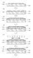
- 4A is a schematic cross-sectional view illustrating the method for manufacturing the thin film transistor according to Embodiment 1.
- FIG. 4B is a schematic cross-sectional view showing the method for manufacturing the thin film transistor according to Embodiment 1.
- FIG. 4C is a schematic cross-sectional view showing the method for manufacturing the thin film transistor according to Embodiment 1.
- FIG. 4A is a schematic cross-sectional view illustrating the method for manufacturing the thin film transistor according to Embodiment 1.
- FIG. 4B is a schematic cross-sectional view showing the method for manufacturing the thin film transistor according to Embodiment 1.
- FIG. 4C is a schematic cross-sectional view showing
- FIG. 5 is a schematic diagram showing a configuration of a chamber that can be used for continuous film formation according to a modification of the first embodiment.
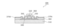
- FIG. 6 is a schematic cross-sectional view of the thin film transistor according to the second embodiment.
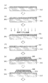
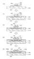
- FIG. 7A is a schematic cross-sectional view showing the method of manufacturing the thin film transistor according to the second embodiment.
- FIG. 7B is a schematic cross-sectional view showing the method for manufacturing the thin film transistor according to Embodiment 2.
- FIG. 7C is a schematic cross-sectional view showing the method for manufacturing the thin film transistor according to Embodiment 2.
- a method of manufacturing a thin film transistor according to the present disclosure includes: a step of forming an oxide semiconductor film over a substrate; a step of forming a silicon film on the oxide semiconductor film; and plasma oxidizing the silicon film, Forming a silicon oxide film, and (ii) supplying oxygen to the oxide semiconductor film.
- the silicon oxide film formed by plasma oxidation prevents the oxide semiconductor surface from being damaged by plasma, and the oxide semiconductor film after oxygen is supplied by plasma oxidation is exposed to the outside air. To prevent. In this manner, plasma damage and oxygen vacancies are suppressed, so that deterioration of physical properties of the oxide semiconductor film can be suppressed. Accordingly, reduction in resistance of the oxide semiconductor film can be suppressed. Therefore, according to the method for manufacturing a thin film transistor according to this embodiment, a thin film transistor in which deterioration of electrical characteristics is suppressed can be manufactured.
- the silicon film in the method of manufacturing a thin film transistor according to the present disclosure, in the step of forming the silicon film, the silicon film may be formed by sputtering.
- the plasma used for sputtering does not contain hydrogen, hydrogen can be prevented from diffusing into the oxide semiconductor film. That is, when sputtering a silicon film, generally, a rare gas element such as argon or krypton is used as an introduction gas. In other words, since a gas containing hydrogen is not used as the introduction gas, hydrogen can be prevented from diffusing into the oxide semiconductor film, and deterioration in electrical characteristics can be suppressed.
- a rare gas element such as argon or krypton
- the oxide semiconductor film and the silicon film may be formed in the same vacuum system in the step of forming the oxide semiconductor film and the step of forming the silicon film. Good.
- the oxide semiconductor film and the silicon film are formed in the same vacuum system, the interface between the oxide semiconductor film and the silicon film can be kept clean. Therefore, it is possible to further suppress deterioration of electrical characteristics.
- the thickness of the silicon film may be 5 nm or less.
- the thickness of the silicon film may be 2 nm or more.
- a silicon oxide film having a sufficient thickness can be formed to prevent the oxide semiconductor film after oxygen is supplied by plasma oxidation from being exposed to the outside air.
- the film thickness of the silicon film is 2 nm to 5 nm
- the film thickness of the silicon film is 2 nm or more and 5 nm or less”.
- the silicon film in the method for manufacturing a thin film transistor according to the present disclosure, in the plasma oxidation step, may be plasma oxidized by surface wave plasma or capacitively coupled plasma having an excitation frequency of 27 MHz or more.
- surface wave plasma or capacitively coupled plasma having an excitation frequency of 27 MHz or more has an advantage that high-density oxygen radicals can be generated and damage caused by ion incidence on the substrate to be processed is small. Therefore, oxygen can be effectively supplied to the oxide semiconductor film while reducing damage to the oxide semiconductor film.
- the method of manufacturing a thin film transistor according to the present disclosure is further patterned by a step of forming a patterned resist on the silicon oxide film, and dry etching the silicon oxide film using the resist as a mask.
- a step of dry etching the silicon oxide layer using the mask is further patterned by a step of forming a patterned resist on the silicon oxide film, and dry etching the silicon oxide film using the resist as a mask.
- the protruding portion of the silicon oxide layer generated by wet etching of the oxide semiconductor film can be removed.
- the oxide semiconductor film may be a transparent amorphous oxide semiconductor.
- the oxide semiconductor film may be InGaZnO.
- a thin film transistor includes a substrate, an oxide semiconductor layer formed over the substrate, and a silicon oxide layer formed over the oxide semiconductor layer, and the silicon oxide layer is an oxide semiconductor layer
- the silicon film formed thereon is formed by plasma oxidation, and the oxide semiconductor layer contains oxygen supplied by plasma oxidation.
- FIG. 1 is a partially cutaway perspective view of an organic EL display device according to the present embodiment.
- an organic EL display device 10 includes a TFT substrate (TFT array substrate) 20 on which a plurality of thin film transistors are arranged, an anode 41 that is a lower electrode, and an EL layer 42 that is a light emitting layer made of an organic material. And it is comprised by the laminated structure with the organic EL element (light emission part) 40 which consists of the cathode 43 which is a transparent upper electrode.
- the TFT substrate 20 has a plurality of pixels 30 arranged in a matrix, and each pixel 30 is provided with a pixel circuit 31.
- the organic EL element 40 is formed corresponding to each of the plurality of pixels 30, and the light emission of each organic EL element 40 is controlled by the pixel circuit 31 provided in each pixel 30.
- the organic EL element 40 is formed on an interlayer insulating film (planarization film) formed so as to cover a plurality of thin film transistors.
- the organic EL element 40 has a configuration in which an EL layer 42 is disposed between the anode 41 and the cathode 43.
- a hole transport layer is further laminated between the anode 41 and the EL layer 42, and an electron transport layer is further laminated between the EL layer 42 and the cathode 43.
- another organic functional layer may be provided between the anode 41 and the cathode 43.
- Each pixel 30 is driven and controlled by a respective pixel circuit 31.
- the TFT substrate 20 includes a plurality of gate wirings (scanning lines) 50 arranged along the row direction of the pixels 30 and a plurality of gate wirings 50 arranged along the column direction of the pixels 30 so as to intersect the gate wiring 50.
- Source wiring (signal wiring) 60 and a plurality of power supply wirings (not shown in FIG. 1) arranged in parallel with the source wiring 60 are formed.
- Each pixel 30 is partitioned by, for example, an orthogonal gate line 50 and a source line 60.
- the gate wiring 50 is connected to the gate electrode of the thin film transistor operating as a switching element included in each pixel circuit 31 for each row.
- the source wiring 60 is connected to the source electrode of the thin film transistor operating as a switching element included in each pixel circuit 31 for each column.
- the power supply wiring is connected to the drain electrode of the thin film transistor operating as a drive element included in each pixel circuit 31 for each column.
- FIG. 2 is an electric circuit diagram showing a configuration of a pixel circuit in the organic EL display device according to the present embodiment.
- the pixel circuit 31 includes a thin film transistor 32 that operates as a driving element, a thin film transistor 33 that operates as a switching element, and a capacitor 34 that stores data to be displayed on the corresponding pixel 30.
- the thin film transistor 32 is a drive transistor for driving the organic EL element 40
- the thin film transistor 33 is a switching transistor for selecting the pixel 30.
- the thin film transistor 32 includes a drain electrode 33d of the thin film transistor 33 and a gate electrode 32g connected to one end of the capacitor 34, a drain electrode 32d connected to the power supply wiring 70, the other end of the capacitor 34, and an anode 41 of the organic EL element 40. And a semiconductor film (not shown).
- the thin film transistor 32 supplies a current corresponding to the data voltage held by the capacitor 34 from the power supply wiring 70 to the anode 41 of the organic EL element 40 through the source electrode 32 s. Thereby, in the organic EL element 40, a drive current flows from the anode 41 to the cathode 43, and the EL layer 42 emits light.
- the thin film transistor 33 includes a gate electrode 33g connected to the gate wiring 50, a source electrode 33s connected to the source wiring 60, a drain electrode 33d connected to one end of the capacitor 34 and the gate electrode 32g of the thin film transistor 32, and a semiconductor film. (Not shown).
- the voltage applied to the source wiring 60 is stored in the capacitor 34 as a data voltage.
- the organic EL display device 10 having the above configuration employs an active matrix system in which display control is performed for each pixel 30 located at the intersection of the gate wiring 50 and the source wiring 60. Thereby, the corresponding organic EL element 40 selectively emits light by the thin film transistors 32 and 33 of each pixel 30 (each sub-pixel R, G, B), and a desired image is displayed.
- the thin film transistor according to this embodiment is a bottom-gate and channel protective thin film transistor.
- FIG. 3 is a schematic cross-sectional view of the thin film transistor 100 according to the present embodiment.
- the thin film transistor 100 includes a substrate 110, a gate electrode 120, a gate insulating layer 130, an oxide semiconductor layer 140, a silicon oxide layer 150, a channel protective layer 160, , A source electrode 170s and a drain electrode 170d.
- the thin film transistor 100 is, for example, the thin film transistor 32 or 33 shown in FIG. That is, the thin film transistor 100 can be used as a driving transistor or a switching transistor.
- the gate electrode 120 corresponds to the gate electrode 32g
- the source electrode 170s corresponds to the source electrode 32s
- the drain electrode 170d corresponds to the drain electrode 32d.
- the gate electrode 120 corresponds to the gate electrode 33g
- the source electrode 170s corresponds to the source electrode 33s
- the drain electrode 170d corresponds to the drain electrode 33d.
- the substrate 110 is a substrate made of a material having electrical insulation.
- the substrate 110 is made of a glass material such as alkali-free glass, quartz glass, or high heat resistance glass, a resin material such as polyethylene, polypropylene, or polyimide, a semiconductor material such as silicon or gallium arsenide, or a metal such as stainless steel coated with an insulating layer.
- the substrate 110 may be a flexible substrate such as a resin substrate.
- the thin film transistor 100 can be used for a flexible display.
- the gate electrode 120 is formed on the substrate 110 in a predetermined shape.
- the film thickness of the gate electrode 120 is, for example, 20 nm to 500 nm.
- the gate electrode 120 is an electrode made of a conductive material.
- a material of the gate electrode 120 molybdenum, aluminum, copper, tungsten, titanium, manganese, chromium, tantalum, niobium, silver, gold, platinum, palladium, indium, nickel, neodymium and other metals, metal alloys, indium oxide Conductive metal oxides such as tin (ITO), aluminum-doped zinc oxide (AZO), and gallium-doped zinc oxide (GZO), and conductive polymers such as polythiophene and polyacetylene can be used.
- the gate electrode 120 may have a multilayer structure in which these materials are stacked.
- the gate insulating layer 130 is formed on the gate electrode 120. Specifically, the gate insulating layer 130 is formed on the gate electrode 120 and the substrate 110 so as to cover the gate electrode 120.
- the film thickness of the gate insulating layer 130 is, for example, 50 nm to 300 nm.
- the gate insulating layer 130 is made of an electrically insulating material.
- the gate insulating layer 130 is a single layer film such as a silicon oxide film, a silicon nitride film, a silicon oxynitride film, an aluminum oxide film, a tantalum oxide film, or a hafnium oxide film, or a stacked film thereof.
- the oxide semiconductor layer 140 is a channel layer of the thin film transistor 100 and is formed above the substrate 110 so as to face the gate electrode 120. Specifically, the oxide semiconductor layer 140 is formed on the gate insulating layer 130 at a position facing the gate electrode 120. For example, the oxide semiconductor layer 140 is formed in an island shape over the gate insulating layer 130 above the gate electrode 120.
- the film thickness of the oxide semiconductor layer 140 is, for example, 20 to 200 nm.
- the oxide semiconductor layer 140 As a material of the oxide semiconductor layer 140, an oxide semiconductor material containing at least one of indium (In), gallium (Ga), and zinc (Zn) is used.
- the oxide semiconductor layer 140 is formed of a transparent amorphous oxide semiconductor (TAOS: Transparent Amorphous Semiconductor) such as amorphous indium gallium zinc oxide (InGaZnO: IGZO).
- TAOS Transparent Amorphous Semiconductor
- InGaZnO IGZO
- the ratio of In: Ga: Zn is, for example, about 1: 1: 1.
- the ratio of In: Ga: Zn may be in the range of 0.8 to 1.2: 0.8 to 1.2: 0.8 to 1.2, but is not limited to this range.
- a thin film transistor in which a channel layer is formed using a transparent amorphous oxide semiconductor has high carrier mobility and is suitable for a large-screen and high-definition display device. Further, since the transparent amorphous oxide semiconductor can be formed at a low temperature, it can be easily formed on a flexible substrate such as a plastic or a film.
- the oxide semiconductor layer 140 contains oxygen supplied by plasma oxidation.
- the oxide semiconductor layer 140 is supplied with oxygen by plasma oxidation from the silicon oxide layer 150 side. Therefore, a region on the silicon oxide layer 150 side of the oxide semiconductor layer 140, specifically, a back channel region contains oxygen supplied by plasma oxidation. Accordingly, oxygen vacancies in the oxide semiconductor layer 140 can be suppressed.
- the silicon oxide layer 150 is formed on the oxide semiconductor layer 140 by plasma-oxidizing the silicon film formed on the oxide semiconductor layer 140.
- the film thickness of the silicon oxide layer 150 is, for example, 2 nm to 5 nm.
- a part of the silicon oxide layer 150 is opened so as to penetrate therethrough. That is, a contact hole for exposing part of the oxide semiconductor layer 140 is formed in the silicon oxide layer 150.
- the oxide semiconductor layer 140 is connected to the source electrodes 170s and 170d through the opened portion (contact hole).
- the end portion of the oxide semiconductor layer 140 protrudes from the silicon oxide layer 150. That is, when viewed in plan, the area of the silicon oxide layer 150 is smaller than the area of the oxide semiconductor layer 140.
- the channel protective layer 160 is formed on the silicon oxide layer 150.
- the channel protective layer 160 is formed on the silicon oxide layer 150, the end of the oxide semiconductor layer 140, and the gate insulating layer 130 so as to cover the ends of the silicon oxide layer 150 and the oxide semiconductor layer 140. It is formed.
- the film thickness of the channel protective layer 160 is, for example, 50 nm to 500 nm.
- the channel protective layer 160 is opened so as to penetrate therethrough. That is, the channel protective layer 160 is formed with a contact hole for exposing part of the oxide semiconductor layer 140. The contact hole is continuous with the contact hole formed in the silicon oxide layer 150.
- the channel protective layer 160 is made of an electrically insulating material.
- the channel protective layer 160 is a film made of an inorganic material such as a silicon oxide film, a silicon nitride film, a silicon oxynitride film, or an aluminum oxide film, or a film made of an inorganic material containing silicon, oxygen, and carbon. Or a laminated film of these.
- the source electrode 170s and the drain electrode 170d are formed in a predetermined shape on the channel protective layer 160. Specifically, the source electrode 170s and the drain electrode 170d are connected to the oxide semiconductor layer 140 through contact holes formed in the silicon oxide layer 150 and the channel protective layer 160, and the substrate horizontal direction is formed on the channel protective layer 160. Are arranged opposite to each other. The source electrode 170s and the drain electrode 170d are 100 nm to 500 nm.
- the source electrode 170s and the drain electrode 170d are electrodes made of a conductive material.
- the material of the source electrode 170s and the drain electrode 170d for example, the same material as that of the gate electrode 120 can be used.
- the thin film transistor 100 includes the silicon oxide layer 150 with a thickness of 2 nm to 5 nm on the oxide semiconductor layer 140.
- the silicon oxide layer 150 is formed by oxidizing a silicon film by plasma oxidation for supplying oxygen to the oxide semiconductor layer 140.
- the silicon oxide layer 150 prevents the surface of the oxide semiconductor layer 140 from being damaged by plasma and prevents the oxide semiconductor layer 140 after being supplied with oxygen by plasma oxidation from being exposed to the outside air. . In this manner, plasma damage and oxygen vacancies are suppressed, so that deterioration of physical properties of the oxide semiconductor layer 140 can be suppressed. Accordingly, reduction in resistance of the oxide semiconductor layer 140 can be suppressed.
- the thin film transistor 100 according to this embodiment can suppress deterioration in electrical characteristics.
- FIGS. 4A to 4C are schematic cross-sectional views showing a method for manufacturing the thin film transistor 100 according to the present embodiment.
- a substrate 110 is prepared, and a gate electrode 120 having a predetermined shape is formed above the substrate 110.
- a metal film is formed on the substrate 110 by sputtering, and the metal film is processed using photolithography and wet etching, so that the gate electrode 120 having a predetermined shape is formed.
- a glass substrate is prepared as the substrate 110, and a molybdenum film (Mo film) and a copper film (Cu film) are sequentially formed on the substrate 110 by sputtering.
- the total film thickness of the Mo film and the Cu film is, for example, 20 nm to 500 nm.
- the gate electrode 120 is formed by patterning the Mo film and the Cu film by photolithography and wet etching.
- the wet etching of the Mo film and the Cu film can be performed using, for example, a chemical solution in which a hydrogen peroxide solution (H 2 O 2 ) and an organic acid are mixed.
- a gate insulating layer 130 is formed above the substrate 110.
- the gate insulating layer 130 is formed on the substrate 110 and the gate electrode 120 by plasma CVD (Chemical Vapor Deposition).
- a gate insulating layer 130 is formed by sequentially forming a silicon nitride film and a silicon oxide film on the substrate 110 by plasma CVD so as to cover the gate electrode 120.
- the film thickness of the gate insulating layer 130 is, for example, 50 nm to 300 nm.
- the silicon nitride film can be formed by using, for example, silane gas (SiH 4 ), ammonia gas (NH 3 ), and nitrogen gas (N 2 ) as the introduction gas.
- the silicon oxide film can be formed by using, for example, silane gas (SiH 4 ) and nitrous oxide gas (N 2 O) as introduction gases.
- an oxide semiconductor film 141 is formed above the substrate 110 and at a position facing the gate electrode 120.
- the oxide semiconductor film 141 is formed over the gate insulating layer 130 by sputtering.
- the thickness of the oxide semiconductor film 141 is, for example, 20 nm to 200 nm.
- the silicon film 151 is formed over the oxide semiconductor film 141.
- a silicon film 151 with a thickness of 2 nm to 5 nm is formed over the oxide semiconductor film 141 by sputtering.
- the target material is silicon
- the introduced gas is argon (Ar) or krypton (Kr) gas
- the pressure is 0.1 Pa to 1.0 Pa
- the power density is 0.03 W / cm 2 to 0.11 W / cm 2. (The input power is 2 kW to 6 kW).
- the silicon film 151 is plasma oxidized.
- a silicon oxide film 152 is formed, and oxygen (oxygen radicals) is supplied to the oxide semiconductor film 141.
- the silicon film 151 is plasma oxidized by surface wave plasma or capacitively coupled plasma (VHF plasma) having an excitation frequency of 27 MHz or more.
- the surface wave plasma has, for example, an excitation frequency of 2.45 GHz, 5.8 GHz, 22.125 GHz, or the like.
- Surface-wave plasma or capacitively coupled plasma having an excitation frequency of 27 MHz or more can generate high-density oxygen radicals and has an advantage that damage caused by ion incidence on a substrate to be processed is small. That is, oxygen can be effectively supplied to the oxide semiconductor film 141 while reducing damage to the oxide semiconductor film 141.
- the rate of increase of the oxide film thickness is limited by the diffusion rate of oxygen. Specifically, the thickness of the formed silicon oxide film increases in proportion to the square root of time.
- the time required to form the silicon oxide film 152 by plasma oxidation increases, and problems such as an increase in manufacturing cost arise. Therefore, for example, by setting the film thickness of the silicon film 151 to 2 nm to 5 nm, plasma oxidation is performed in a short time (eg, about several tens of seconds to 10 minutes), and oxygen is supplied to the oxide semiconductor film 141. it can. Thus, since the time required for plasma oxidation can be shortened, the manufacturing cost can be reduced.
- a resist 180 patterned in a predetermined shape is formed on the silicon oxide film 152.
- the resist 180 is patterned by photolithography.
- the film thickness of the resist 180 is about 2 ⁇ m.
- the resist 180 is formed using a photoresist made of a polymer compound containing a photosensitive functional molecule. After applying a photoresist on the silicon oxide film 152, pre-baking, exposure, development, and post-baking are performed in this order to form a patterned resist 180.
- a patterned silicon oxide layer 153 is formed on the oxide semiconductor film 141.
- the patterned silicon oxide layer 153 is formed by dry etching the silicon oxide film 152 using the resist 180 as a mask.
- etching for example, reactive ion etching (RIE) can be used.
- RIE reactive ion etching
- carbon tetrafluoride (CF 4 ) and oxygen gas (O 2 ) can be used as the etching gas.
- Parameters such as gas flow rate, pressure, applied power, and frequency are appropriately set depending on the substrate size, etching film thickness, and the like.
- a patterned oxide semiconductor layer 140 is formed on the gate insulating layer 130.
- the oxide semiconductor layer 140 is formed by wet etching the oxide semiconductor film 141 using the resist 180 and the silicon oxide layer 153 as a mask.
- the oxide semiconductor layer 140 is formed by wet etching of amorphous InGaZnO formed over the gate insulating layer 130.
- wet etching of InGaZnO can be performed using a chemical solution in which phosphoric acid (H 3 PO 4 ), nitric acid (HNO 3 ), acetic acid (CH 3 COOH), and water are mixed.
- the chemical solution used for the wet etching wraps around, so that the end portion of the oxide semiconductor layer 140 is cut below the end portion of the silicon oxide layer 153 as shown in FIG. 4B (i). In other words, the end portion of the silicon oxide layer 153 protrudes outward from the oxide semiconductor layer 140 in a plan view.
- the end of the resist 180 is retracted by ashing.
- the resist 180 is combined with oxygen radicals in the plasma and evaporated. Therefore, since the resist 180 is removed by evaporation from the portion exposed to the oxygen plasma, that is, the surface of the resist 180, the end portion of the resist 180 gradually recedes. That is, the resist 180 is degenerated by ashing.
- a resist 181 whose end is recessed is formed on the silicon oxide layer 153. Note that since the resist 180 is shrunk as a whole, the film thickness of the resist 181 whose end is recessed is smaller than the film thickness of the resist 180.
- the time for ashing with oxygen plasma is determined by the width of the protruding portion of the silicon oxide layer 153, for example. In other words, the ashing time is determined so that the degenerated resist 181 has a size equal to or smaller than that of the oxide semiconductor layer 140 in a plan view.
- the silicon oxide layer 154 is formed by dry etching the silicon oxide layer 153 using the resist 181 whose end is recessed as a mask. Accordingly, the protruding portion (see (i) of FIG. 4B) of the silicon oxide layer 153 generated by wet etching of the oxide semiconductor film 141 can be removed.
- the resist 181 is removed.
- the resist 181 is removed by ashing using oxygen plasma.
- the resist 181 is removed by ashing in a sufficiently longer time than when the resist 180 is degenerated.
- a channel protective film 161 is formed over the oxide semiconductor layer 140.
- the channel protective film 161 is formed over the silicon oxide layer 154, the oxide semiconductor layer 140, and the gate insulating layer 130 so as to cover the silicon oxide layer 154 and the oxide semiconductor layer 140.
- the channel protective film 161 can be formed by forming a silicon oxide film on the entire surface by plasma CVD.
- the thickness of the silicon oxide film is 50 nm to 500 nm.
- the silicon oxide film can be formed by using, for example, silane gas (SiH 4 ) and nitrous oxide gas (N 2 O) as introduction gases.
- the channel protection film 161 and the silicon oxide layer 154 are patterned into a predetermined shape, thereby forming the patterned channel protection layer 160 and the silicon oxide layer 150.
- a contact hole is formed in the channel protective film 161 and the silicon oxide layer 154 so that a part of the oxide semiconductor layer 140 is exposed.
- the contact hole is formed by etching away part of the channel protective film 161 and the silicon oxide layer 154.
- a part of the channel protective film 161 and the silicon oxide layer 154 is etched by photolithography and dry etching, so that a contact is formed on a region that becomes a source contact region and a drain contact region of the oxide semiconductor layer 140.
- a hole is formed.
- the channel protective film 161 is a silicon oxide film
- reactive ion etching (RIE) can be used as dry etching.
- carbon tetrafluoride (CF 4 ) and oxygen gas (O 2 ) can be used as the etching gas. Parameters such as gas flow rate, pressure, applied power, and frequency are appropriately set depending on the substrate size, etching film thickness, and the like.
- a metal film 171 is formed so as to be connected to the oxide semiconductor layer 140 through the contact hole. Specifically, a metal film 171 is formed on the channel protective layer 160 and in the contact hole.
- the metal film 171 is formed by sequentially depositing a Mo film, a Cu film, and a CuMn film on the channel protective layer 160 and in the contact hole by sputtering.
- the film thickness of the metal film 171 is, for example, 100 nm to 500 nm.
- a source electrode 170s and a drain electrode 170d connected to the oxide semiconductor layer 140 are formed.
- the source electrode 170 s and the drain electrode 170 d having a predetermined shape are formed on the channel protective layer 160 so as to fill the contact holes formed in the channel protective layer 160.
- the source electrode 170s and the drain electrode 170d are formed on the channel protective layer 160 and in the contact hole with a space therebetween. More specifically, the source electrode 170s and the drain electrode 170d are formed by patterning the metal film 171 by photolithography and wet etching. The wet etching of the Mo film, the Cu film, and the CuMn film can be performed using, for example, a chemical solution in which hydrogen peroxide solution (H 2 O 2 ) and an organic acid are mixed.
- H 2 O 2 hydrogen peroxide solution
- the thin film transistor 100 can be manufactured as described above.
- the method for manufacturing the thin film transistor according to this embodiment includes a step of forming the oxide semiconductor film 141 over the substrate 110, a step of forming the silicon film 151 over the oxide semiconductor film 141, and a silicon (I) forming a silicon oxide film 152 by plasma oxidizing the film 151 and (ii) supplying oxygen to the oxide semiconductor film 141.
- the silicon oxide film 152 formed by plasma oxidation prevents the surface of the oxide semiconductor film 141 from being damaged by plasma, and the oxide semiconductor film 141 after oxygen is supplied by plasma oxidation. Is not exposed to the open air. In this manner, plasma damage and oxygen vacancies are suppressed, so that deterioration of physical properties of the oxide semiconductor film 141 can be prevented. That is, the silicon oxide film 152 can reduce process damage due to a subsequent film formation process.
- oxygen vacancies can be suppressed, so that the density of oxygen vacancies in the oxide semiconductor film 141 can be reduced. That is, the number of carriers generated in the oxide semiconductor film 141 can be reduced, and the resistance of the oxide semiconductor film 141 can be reduced. Therefore, according to the present embodiment, it is possible to manufacture the thin film transistor 100 in which deterioration of electrical characteristics is suppressed.
- the silicon film 151 is formed over the oxide semiconductor film 141. At this time, the oxide semiconductor film 141 and the silicon film are formed in the same vacuum system. A film 151 may be formed. In other words, the oxide semiconductor film 141 and the silicon film 151 may be formed by continuous film formation.
- film formation in the same vacuum system means film formation without exposing the target substrate to atmospheric pressure.
- the oxide semiconductor film 141 and the silicon film 151 are connected by a continuous film formation process performed in a vacuum system in which a plurality of vacuum chambers are connected via a gate valve and a substrate is transferred while maintaining a vacuum. May be formed.
- FIG. 5 is a diagram illustrating a configuration example of a chamber that can be used for continuous film formation according to a modification of the present embodiment.
- a film forming apparatus 200 shown in FIG. 5 is a multi-chamber type film forming apparatus in which a plurality of chambers are connected by gate valves.
- the film forming apparatus 200 includes two film forming chambers 210 and 211, a vacuum transfer chamber 220, and gate valves 230 to 233 provided between the chambers.
- the film formation chamber 211 is a film formation chamber for forming the silicon film 151. Therefore, for example, the film formation chamber 211 is a chamber for performing sputtering in an Ar or Kr atmosphere using a target material made of silicon.
- the vacuum transfer chamber 220 is a chamber for transferring a substrate.
- the substrate is transferred from the film formation chamber 210 to the film formation chamber 211 by a transfer arm or the like provided inside the vacuum transfer chamber 220.
- the gate valves 230 to 233 are open / close valves.
- the gate valve 230 is opened when the substrate is placed in the film forming chamber 210.
- the gate valve 231 and the gate valve 232 are opened when the substrate is transferred from the film formation chamber 210 to the film formation chamber 211.
- the gate valve 233 is opened when the substrate is taken out from the film formation chamber 211.
- the gate valves 230 to 233 are closed while sputtering is performed in the film formation chamber 210 and the film formation chamber 211.
- the film forming chambers 210 and 211 and the vacuum transfer chamber 220 are kept in the same vacuum system. That is, each chamber is kept in the same vacuum system after the substrate is placed in the deposition chamber 210 until the substrate is taken out from the deposition chamber 211.
- the oxide semiconductor film 141 and the silicon film 151 can be continuously formed without being exposed to the outside air. Therefore, the interface between the oxide semiconductor film 141 and the silicon film 151 can be kept clean. That is, after the oxide semiconductor film 141 is formed, the silicon film 151 can be formed while the surface thereof is kept clean.
- the silicon film 151 is formed by sputtering in an Ar or Kr atmosphere. In other words, since a gas containing hydrogen is not used, diffusion of hydrogen into the oxide semiconductor film 141 can be suppressed.
- the plurality of film forming chambers 210 and 211 are connected via the gate valves 230 to 233, and the continuous deposition performed in the vacuum system provided with the vacuum transfer chamber 220 for transferring the substrate while maintaining the vacuum.
- the oxide semiconductor film 141 and the silicon film 151 can be formed. Accordingly, deterioration of electrical characteristics of the oxide semiconductor film 141 can be further suppressed.
- the same vacuum system may be configured without using the vacuum transfer chamber 220.
- continuous film formation may be performed in the same vacuum chamber instead of a plurality of vacuum chambers.
- the oxide semiconductor film 141 and the silicon film 151 can be continuously formed in the same vacuum system by disposing the substrate in the same vacuum chamber and changing the target material and the introduced gas.
- the thin film transistor according to the present embodiment is a top-gate thin film transistor.
- FIG. 6 is a schematic cross-sectional view of the thin film transistor 300 according to this embodiment.
- the thin film transistor 300 includes a substrate 310, a gate electrode 320, a gate insulating layer 330, an oxide semiconductor layer 340, a silicon oxide layer 350, an insulating layer 360, A source electrode 370s and a drain electrode 370d are provided.
- the thin film transistor 300 is, for example, the thin film transistor 32 or 33 shown in FIG. That is, the thin film transistor 300 can be used as a driving transistor or a switching transistor.
- the gate electrode 320 corresponds to the gate electrode 32g
- the source electrode 370s corresponds to the source electrode 32s
- the drain electrode 370d corresponds to the drain electrode 32d.
- the gate electrode 320 corresponds to the gate electrode 33g
- the source electrode 370s corresponds to the source electrode 33s
- the drain electrode 370d corresponds to the drain electrode 33d.
- the substrate 310 is a substrate made of an electrically insulating material.
- the substrate 310 is made of a glass material such as alkali-free glass, quartz glass, or high heat resistance glass, a resin material such as polyethylene, polypropylene, or polyimide, a semiconductor material such as silicon or gallium arsenide, or a metal such as stainless steel coated with an insulating layer.
- the substrate 310 may be a flexible substrate such as a resin substrate.
- the thin film transistor 300 can be used for a flexible display.
- the gate electrode 320 is formed in a predetermined shape above the substrate 310.
- the gate electrode 320 is formed at a position facing the oxide semiconductor layer 340 and over the gate insulating layer 330.
- the material and thickness of the gate electrode 320 the same material and thickness as those of the gate electrode 120 according to Embodiment 1 can be used.
- the gate insulating layer 330 is formed between the gate electrode 320 and the oxide semiconductor layer 340. Specifically, the gate insulating layer 330 is formed on the silicon oxide layer 350.
- the gate insulating layer 330 is made of an electrically insulating material. For example, as the material and thickness of the gate insulating layer 330, the same material and thickness as those of the gate insulating layer 130 according to Embodiment 1 can be used.
- the oxide semiconductor layer 340 is a channel layer of the thin film transistor 300 and is formed over the substrate 310 so as to face the gate electrode 320.
- the oxide semiconductor layer 340 is formed in an island shape over the substrate 310.
- the same material and thickness as those of the oxide semiconductor layer 140 according to Embodiment 1 can be used.
- the oxide semiconductor layer 340 contains oxygen supplied by plasma oxidation.
- the oxide semiconductor layer 340 is supplied with oxygen by plasma oxidation from the silicon oxide layer 350 side. Therefore, a region on the silicon oxide layer 350 side of the oxide semiconductor layer 340, specifically, a front channel region contains oxygen supplied by plasma oxidation. Accordingly, oxygen vacancies in the oxide semiconductor layer 140 can be suppressed.
- the silicon oxide layer 350 is formed on the oxide semiconductor layer 340 by plasma oxidizing a silicon film formed on the oxide semiconductor layer 340.
- the film thickness of the silicon oxide layer 350 is, for example, 2 nm to 5 nm.
- the insulating layer 360 is formed over the substrate 310, the oxide semiconductor layer 340, and the gate electrode 320.
- the insulating layer 360 is formed over the substrate 310, the oxide semiconductor layer 340, and the gate electrode 320 so as to cover the gate electrode 320 and the end portion of the oxide semiconductor layer 340.
- the material and thickness of the insulating layer 360 the same material and thickness as those of the channel protective layer 160 according to Embodiment 1 can be used.
- a part of the insulating layer 360 is opened so as to penetrate therethrough. That is, a contact hole for exposing part of the oxide semiconductor layer 340 is formed in the insulating layer 360.
- the source electrode 370s and the drain electrode 370d are formed in a predetermined shape on the insulating layer 360. Specifically, the source electrode 370 s and the drain electrode 370 d are connected to the oxide semiconductor layer 340 through contact holes formed in the insulating layer 360, and are disposed opposite to each other on the insulating layer 360 in the horizontal direction of the substrate. ing. As the material and film thickness of the source electrode 370s and the drain electrode 370d, the same material and film thickness as the source electrode 170s and the drain electrode 170d according to Embodiment 1 can be used.
- the thin film transistor 300 includes the silicon oxide layer 350 with a thickness of 2 nm to 5 nm over the oxide semiconductor layer 340.
- the silicon oxide layer 350 is formed by oxidizing a silicon film by plasma oxidation for supplying oxygen to the oxide semiconductor layer 340.
- the silicon oxide layer 350 prevents the surface of the oxide semiconductor layer 340 from being damaged by plasma and prevents the oxide semiconductor layer 340 after being supplied with oxygen by plasma oxidation from being exposed to the outside air. . In this manner, plasma damage and oxygen vacancies are suppressed, so that deterioration of physical properties of the oxide semiconductor layer 340 can be suppressed. Accordingly, reduction in resistance of the oxide semiconductor layer 340 can be suppressed.
- the thin film transistor 300 according to this embodiment can suppress deterioration in electrical characteristics.
- the thin film transistor 300 according to the present embodiment can suppress deterioration of electrical characteristics.
- FIGS. 7A to 7C are schematic cross-sectional views showing a method for manufacturing the thin film transistor 300 according to the present embodiment.
- a substrate 310 is prepared, and an oxide semiconductor film 341 is formed over the substrate 310.
- the oxide semiconductor film 341 is formed over the substrate 310 by sputtering.
- the sputtering conditions are the same as the sputtering conditions for forming the oxide semiconductor film 141 according to Embodiment 1, for example (see FIG. 4A (c)).
- a silicon film 351 is formed over the oxide semiconductor film 341.
- a silicon film 351 with a thickness of 2 nm to 5 nm is formed over the oxide semiconductor film 341 by sputtering.
- the sputtering conditions are the same as the sputtering conditions for forming the silicon film 151 according to Embodiment 1, for example (see (d) of FIG. 4A).
- the silicon film 351 is plasma oxidized.
- Plasma oxidation of the silicon film 351 forms a silicon oxide film 352 and supplies oxygen to the oxide semiconductor film 341 as shown in FIG. 7A (d).
- the plasma oxidation conditions are, for example, the same as the plasma oxidation conditions according to Embodiment 1 (see (e) and (f) of FIG. 4A). Therefore, oxygen can be effectively supplied to the oxide semiconductor film 341 while reducing damage to the oxide semiconductor film 341.
- a resist 380 patterned into a predetermined shape is formed on the silicon oxide film 352.
- the resist 380 is patterned by photolithography.
- the formation of the resist 380 is performed by, for example, the same method as the formation of the resist 180 according to Embodiment 1 (see (g) of FIG. 4B).
- a patterned silicon oxide layer 353 is formed on the oxide semiconductor film 341.
- the patterned silicon oxide layer 353 is formed by dry etching the silicon oxide film 352 using the resist 380 as a mask.
- the dry etching of the silicon oxide film 352 is performed, for example, by the same method as the dry etching of the silicon oxide film 152 according to Embodiment 1 (see (h) in FIG. 4B).
- a patterned oxide semiconductor layer 340 is formed on the substrate 310.
- the oxide semiconductor layer 340 is formed by wet etching the oxide semiconductor film 341 using the resist 380 and the silicon oxide layer 353 as a mask.
- the oxide semiconductor layer 340 is formed by wet etching of amorphous InGaZnO formed over the substrate 310.
- wet etching of InGaZnO can be performed using a chemical solution in which phosphoric acid (H 3 PO 4 ), nitric acid (HNO 3 ), acetic acid (CH 3 COOH), and water are mixed.
- an end portion of the oxide semiconductor layer 340 is formed below the end portion of the silicon oxide layer 353 as illustrated in FIG. It is shaved. In other words, the end portion of the silicon oxide layer 353 protrudes outward from the oxide semiconductor layer 340 in a plan view.
- the end of the resist 380 is retracted by ashing.
- the resist 381 is degenerated by ashing, whereby the resist 381 whose end is recessed is formed on the silicon oxide layer 353.
- the ashing of the resist 380 for retracting the end portion is performed, for example, by the same method as the ashing of the resist 180 according to Embodiment 1 (see (j) in FIG. 4B).
- the silicon oxide layer 353 is dry-etched using the resist 381 whose end is recessed as a mask, thereby forming a silicon oxide layer 354. Accordingly, the protruding portion (see FIG. 7B (g)) of the silicon oxide layer 353 generated by wet etching of the oxide semiconductor film 341 can be removed.
- the resist 381 is removed.
- the resist 381 is removed by ashing using oxygen plasma.
- the resist 381 is removed by ashing in a sufficiently longer time than when the resist 380 is degenerated.
- a gate insulating film 331 is formed on the silicon oxide layer 354.
- the gate insulating film 331 is formed by plasma CVD over the silicon oxide layer 354, the oxide semiconductor layer 340, and the substrate 310 so as to cover the silicon oxide layer 354 and the end portion of the oxide semiconductor layer 340.
- the gate insulating film 331 is formed by, for example, the same method as the gate insulating layer 130 according to Embodiment 1 (see FIG. 4A (b)).
- a metal film 321 is formed on the gate insulating film 331.
- the metal film 321 is formed over the gate insulating film 331 by sputtering.
- a Mo film and a Cu film are sequentially formed on the gate insulating film 331 by sputtering.
- the total film thickness of the Mo film and the Cu film is, for example, 20 nm to 500 nm.
- the metal film 321, the gate insulating film 331 and the silicon oxide layer 354 are patterned to form the gate electrode 320, the gate insulating layer 330 and the silicon oxide layer 350.
- the metal film 321 is patterned by wet etching, and the gate insulating film 331 and the silicon oxide layer 354 are patterned by dry etching.
- the wet etching of the metal film 321 can be performed using, for example, a chemical solution in which hydrogen peroxide solution (H 2 O 2 ) and an organic acid are mixed. Further, for example, reactive ion etching (RIE) can be used for dry etching of the gate insulating film 331 and the silicon oxide layer 354. At this time, for example, carbon tetrafluoride (CF 4 ) and oxygen gas (O 2 ) can be used as the etching gas. Parameters such as gas flow rate, pressure, applied power, and frequency are appropriately set depending on the substrate size, etching film thickness, and the like.
- RIE reactive ion etching
- the oxide semiconductor layer 340 since part of the oxide semiconductor layer 340 is exposed, it is affected by dry etching. Specifically, the resistance of the exposed portion of the oxide semiconductor layer 340 is reduced. Therefore, a good source contact and drain contact can be realized by using the low resistance portion as a connection region with the source electrode or the drain electrode.
- an insulating film 361 is formed over the gate electrode 320 and the oxide semiconductor layer 340.
- the insulating film 361 is formed over the substrate 310, the gate electrode 320, and the oxide semiconductor layer 340 so as to cover the gate electrode 320 and the oxide semiconductor layer 340.
- the insulating film 361 is formed by, for example, the same method as the channel protective film 161 according to Embodiment 1 (see (m) in FIG. 4C).
- the insulating film 360 is patterned into a predetermined shape to form a patterned insulating layer 360. Specifically, a contact hole is formed in the insulating film 361 so that part of the oxide semiconductor layer 340 is exposed. For example, a part of the insulating film 361 is removed by etching to form a contact hole.
- the contact hole is formed by, for example, the same method as the formation of the contact hole in the channel protective film 161 according to Embodiment 1 (see (n) in FIG. 4C).
- a metal film 371 is formed so as to be connected to the oxide semiconductor layer 340 through the contact hole. Specifically, a metal film 371 is formed on the insulating layer 360 and in the contact hole. The formation of the metal film 371 is performed, for example, by the same method as the formation of the metal film 171 according to Embodiment 1 (see (o) in FIG. 4C).
- a source electrode 370s and a drain electrode 370d connected to the oxide semiconductor layer 340 are formed.
- the source electrode 370 s and the drain electrode 370 d having a predetermined shape are formed on the insulating layer 360 so as to fill the contact holes formed in the insulating layer 360.
- the formation of the source electrode 370s and the drain electrode 370d is performed by, for example, the same method as the formation of the source electrode 170s and the drain electrode 170d according to Embodiment 1 (see (p) in FIG. 4C).
- the thin film transistor 300 can be manufactured as described above.
- the manufacturing method of the thin film transistor includes the step of forming the oxide semiconductor film 341 over the substrate 310, the step of forming the silicon film 351 over the oxide semiconductor film 341, and the silicon (I) forming a silicon oxide film 352 and (ii) supplying oxygen to the oxide semiconductor film 341 by plasma oxidizing the film 351.
- the silicon oxide film 352 formed by plasma oxidation prevents the surface of the oxide semiconductor film 341 from being damaged by plasma, and the oxide semiconductor film 341 after oxygen is supplied by plasma oxidation. Is not exposed to the open air. In this manner, plasma damage and oxygen vacancies are suppressed, so that deterioration of physical properties of the oxide semiconductor film 341 can be prevented.
- oxygen vacancies can be suppressed, and thus the oxygen vacancy density in the oxide semiconductor film 341 can be reduced. That is, in the oxide semiconductor film 341, the number of carrier generation sources can be reduced, and reduction in resistance of the oxide semiconductor film 341 can be suppressed. Therefore, according to this embodiment, it is possible to manufacture the thin film transistor 300 in which deterioration of electrical characteristics is suppressed.
- the region on the silicon oxide film 352 side is a region on the gate electrode 320 side, that is, a front channel region. In this manner, in the case of the top gate type thin film transistor 300, lowering of the resistance of the front channel region is suppressed, so that deterioration of electrical characteristics is further suppressed.
- Embodiments 1 and 2 have been described as examples of the technology disclosed in the present application. However, the technology in the present disclosure is not limited to these, and can also be applied to embodiments in which changes, replacements, additions, omissions, and the like are appropriately performed.
- surface wave plasma or capacitively coupled plasma having an excitation frequency of 27 MHz or more is used as an example of plasma processing, but the present invention is not limited to this.
- Embodiment 1 a bottom gate type and channel protection type thin film transistor has been described, but a bottom gate type and channel etch type thin film transistor may be used.
- the channel protective film 161 after the channel protective film 161 is formed on the entire surface, contacts for the source electrode 170s and the drain electrode 170d are formed on the channel protective film 161.
- a hole is formed, it is not limited to this.
- the channel protective layer 160 that is previously patterned into a predetermined shape so that the oxide semiconductor layer 140 is exposed may be formed.
- the channel protective layer 160 may be formed so that a part of the oxide semiconductor layer 140 is exposed.
- the source electrode 170s and the drain electrode 170d may be formed so as to be connected to the oxide semiconductor layer 140 at the exposed portions.
- the oxide semiconductor used for the oxide semiconductor layer is not limited to amorphous InGaZnO.
- a polycrystalline semiconductor such as polycrystalline InGaO may be used.
- an organic EL display device is described as a display device using a thin film transistor.
- the thin film transistor in the above embodiment is also applied to other display devices using an active matrix substrate such as a liquid crystal display device. can do.
- the display device such as the organic EL display device described above can be used as a flat panel display, and is applied to all electronic devices having a display panel such as a television set, a personal computer, and a mobile phone. be able to. In particular, it is suitable for a large-screen and high-definition display device.
- the thin film transistor and the manufacturing method thereof according to the present disclosure can be used for a display device such as an organic EL display device, for example.
- Organic EL display device 20 TFT substrate 30 Pixel 31 Pixel circuit 32, 33, 100, 300 Thin film transistor 32d, 33d, 170d, 370d Drain electrode 32g, 33g, 120, 320 Gate electrode 32s, 33s, 170s, 370s Source electrode 34 Capacitor 40 Organic EL element 41 Anode 42 EL layer 43 Cathode 50 Gate wiring 60 Source wiring 70 Power supply wiring 110, 310 Substrate 130, 330 Gate insulating layer 140, 340 Oxide semiconductor layers 141, 341 Oxide semiconductor films 150, 153, 154, 350, 353, 354 Silicon oxide layer 151, 351 Silicon film 152, 352 Silicon oxide film 160 Channel protective layer 161 Channel protective film 171, 321, 371 Metal film 180, 181, 380, 381 Resist 200 Film device 210, 211 Film formation chamber 220 Vacuum transfer chamber 230, 231, 232, 233 Gate valve 331 Gate insulating film 360 Insulating layer 361 Insulating film
Landscapes
- Thin Film Transistor (AREA)
- Weting (AREA)
- Formation Of Insulating Films (AREA)
- Physics & Mathematics (AREA)
- Engineering & Computer Science (AREA)
- Plasma & Fusion (AREA)
Abstract
Description
本開示に係る薄膜トランジスタの製造方法は、基板の上方に酸化物半導体膜を形成する工程と、酸化物半導体膜上にシリコン膜を形成する工程と、シリコン膜をプラズマ酸化することで、(i)シリコン酸化膜を形成し、かつ、(ii)酸化物半導体膜に酸素を供給する工程とを含む。
[有機EL表示装置]
まず、本実施の形態に係る有機EL表示装置10の構成について、図1を用いて説明する。図1は、本実施の形態に係る有機EL表示装置の一部切り欠き斜視図である。
以下では、本実施の形態に係る薄膜トランジスタについて、図3を用いて説明する。なお、本実施の形態に係る薄膜トランジスタは、ボトムゲート型、かつ、チャネル保護型の薄膜トランジスタである。
続いて、本実施の形態に係る薄膜トランジスタの製造方法について、図4A~図4Cを用いて説明する。図4A~図4Cは、本実施の形態に係る薄膜トランジスタ100の製造方法を示す概略断面図である。
以上のように、本実施の形態に係る薄膜トランジスタの製造方法は、基板110の上方に酸化物半導体膜141を形成する工程と、酸化物半導体膜141上にシリコン膜151を形成する工程と、シリコン膜151をプラズマ酸化することで、(i)シリコン酸化膜152を形成し、かつ、(ii)酸化物半導体膜141に酸素を供給する工程とを含む。
次に、実施の形態2について説明する。なお、本実施の形態に係る有機EL表示装置の構成は、実施の形態1に係る有機EL表示装置10の構成と同様であるので、その説明は省略し、薄膜トランジスタについて説明する。
以下では、本実施の形態に係る薄膜トランジスタについて説明する。なお、本実施の形態に係る薄膜トランジスタは、トップゲート型の薄膜トランジスタである。
続いて、本実施の形態に係る薄膜トランジスタの製造方法について、図7A~図7Cを用いて説明する。図7A~図7Cは、本実施の形態に係る薄膜トランジスタ300の製造方法を示す概略断面図である。
以上のように、本実施の形態に係る薄膜トランジスタの製造方法は、基板310の上方に酸化物半導体膜341を形成する工程と、酸化物半導体膜341上にシリコン膜351を形成する工程と、シリコン膜351をプラズマ酸化することで、(i)シリコン酸化膜352を形成し、かつ、(ii)酸化物半導体膜341に酸素を供給する工程とを含む。
以上のように、本出願において開示する技術の例示として、実施の形態1及び2を説明した。しかしながら、本開示における技術は、これらに限定されず、適宜、変更、置き換え、付加、省略などを行った実施の形態にも適用可能である。
20 TFT基板
30 画素
31 画素回路
32、33、100、300 薄膜トランジスタ
32d、33d、170d、370d ドレイン電極
32g、33g、120、320 ゲート電極
32s、33s、170s、370s ソース電極
34 キャパシタ
40 有機EL素子
41 陽極
42 EL層
43 陰極
50 ゲート配線
60 ソース配線
70 電源配線
110、310 基板
130、330 ゲート絶縁層
140、340 酸化物半導体層
141、341 酸化物半導体膜
150、153、154、350、353、354 酸化シリコン層
151、351 シリコン膜
152、352 シリコン酸化膜
160 チャネル保護層
161 チャネル保護膜
171、321、371 金属膜
180、181、380、381 レジスト
200 成膜装置
210、211 成膜チャンバー
220 真空搬送チャンバー
230、231、232、233 ゲートバルブ
331 ゲート絶縁膜
360 絶縁層
361 絶縁膜
Claims (10)
- 基板の上方に酸化物半導体膜を形成する工程と、
前記酸化物半導体膜上にシリコン膜を形成する工程と、
前記シリコン膜をプラズマ酸化することで、(i)シリコン酸化膜を形成し、かつ、(ii)前記酸化物半導体膜に酸素を供給する工程とを含む
薄膜トランジスタの製造方法。 - 前記シリコン膜を形成する工程では、スパッタリングによって前記シリコン膜を形成する
請求項1に記載の薄膜トランジスタの製造方法。 - 前記酸化物半導体膜を形成する工程及び前記シリコン膜を形成する工程では、同一真空系内で、前記酸化物半導体膜と前記シリコン膜とを形成する
請求項1又は2に記載の薄膜トランジスタの製造方法。 - 前記シリコン膜の厚さは、5nm以下である
請求項1~3のいずれか1項に記載の薄膜トランジスタの製造方法。 - 前記シリコン膜の厚さは、2nm以上である
請求項1~4のいずれか1項に記載の薄膜トランジスタの製造方法。 - 前記プラズマ酸化する工程では、表面波プラズマ、又は、励起周波数が27MHz以上の容量結合プラズマによって、前記シリコン膜をプラズマ酸化する
請求項1~5のいずれか1項に記載の薄膜トランジスタの製造方法。 - 前記薄膜トランジスタの製造方法は、さらに、
前記シリコン酸化膜上に、パターニングされたレジストを形成する工程と、
前記レジストをマスクとして用いて前記シリコン酸化膜をドライエッチングすることで、パターニングされた酸化シリコン層を形成する工程と、
前記レジスト及び前記酸化シリコン層をマスクとして用いて前記酸化物半導体膜をウェットエッチングする工程と、
アッシングにより前記レジストの端部を後退させる工程と、
端部が後退した前記レジストをマスクとして用いて前記酸化シリコン層をドライエッチングする工程とを含む
請求項1~6のいずれか1項に記載の薄膜トランジスタの製造方法。 - 前記酸化物半導体膜は、透明アモルファス酸化物半導体である
請求項1~7のいずれか1項に記載の薄膜トランジスタの製造方法。 - 前記酸化物半導体膜は、InGaZnOである
請求項1~8のいずれか1項に記載の薄膜トランジスタの製造方法。 - 基板と、
前記基板の上方に形成された酸化物半導体層と、
前記酸化物半導体層上に形成された酸化シリコン層とを備え、
前記酸化シリコン層は、前記酸化物半導体層上に形成されたシリコン膜をプラズマ酸化することで形成され、
前記酸化物半導体層は、前記プラズマ酸化によって供給された酸素を含む
薄膜トランジスタ。
Priority Applications (2)
| Application Number | Priority Date | Filing Date | Title |
|---|---|---|---|
| US15/100,384 US20160300954A1 (en) | 2013-12-02 | 2014-08-26 | Thin-film transistor and manufacturing method for same |
| JP2015551370A JP6142300B2 (ja) | 2013-12-02 | 2014-08-26 | 薄膜トランジスタの製造方法 |
Applications Claiming Priority (2)
| Application Number | Priority Date | Filing Date | Title |
|---|---|---|---|
| JP2013-249375 | 2013-12-02 | ||
| JP2013249375 | 2013-12-02 |
Publications (1)
| Publication Number | Publication Date |
|---|---|
| WO2015083303A1 true WO2015083303A1 (ja) | 2015-06-11 |
Family
ID=53273094
Family Applications (1)
| Application Number | Title | Priority Date | Filing Date |
|---|---|---|---|
| PCT/JP2014/004370 Ceased WO2015083303A1 (ja) | 2013-12-02 | 2014-08-26 | 薄膜トランジスタ及びその製造方法 |
Country Status (3)
| Country | Link |
|---|---|
| US (1) | US20160300954A1 (ja) |
| JP (1) | JP6142300B2 (ja) |
| WO (1) | WO2015083303A1 (ja) |
Cited By (1)
| Publication number | Priority date | Publication date | Assignee | Title |
|---|---|---|---|---|
| CN106876334A (zh) * | 2017-03-10 | 2017-06-20 | 京东方科技集团股份有限公司 | 阵列基板的制造方法及阵列基板 |
Families Citing this family (6)
| Publication number | Priority date | Publication date | Assignee | Title |
|---|---|---|---|---|
| CN107078163A (zh) * | 2014-10-28 | 2017-08-18 | 凸版印刷株式会社 | 薄膜晶体管阵列及其制造方法 |
| KR20160119935A (ko) * | 2015-04-06 | 2016-10-17 | 삼성디스플레이 주식회사 | 표시장치 및 그 제작 방법 |
| KR101992917B1 (ko) * | 2016-11-30 | 2019-06-25 | 엘지디스플레이 주식회사 | 표시 장치용 기판과, 그를 포함하는 유기 발광 표시 장치 및 그 제조 방법 |
| JP6960807B2 (ja) * | 2017-08-31 | 2021-11-05 | 株式会社ジャパンディスプレイ | 表示装置及びその製造方法 |
| CN116207157A (zh) | 2021-12-08 | 2023-06-02 | 厦门天马显示科技有限公司 | 氧化物半导体薄膜晶体管器件及其制造方法 |
| US20250133820A1 (en) * | 2023-10-20 | 2025-04-24 | Taiwan Semiconductor Manufacturing Company, Ltd. | Insertion layer between channel and passivation for transistor |
Citations (3)
| Publication number | Priority date | Publication date | Assignee | Title |
|---|---|---|---|---|
| JP2011199272A (ja) * | 2010-02-26 | 2011-10-06 | Semiconductor Energy Lab Co Ltd | 半導体装置の作製方法 |
| JP2012238851A (ja) * | 2011-04-27 | 2012-12-06 | Semiconductor Energy Lab Co Ltd | 半導体装置の作製方法 |
| JP2013038401A (ja) * | 2011-07-08 | 2013-02-21 | Semiconductor Energy Lab Co Ltd | 半導体装置及び半導体装置の作製方法 |
Family Cites Families (7)
| Publication number | Priority date | Publication date | Assignee | Title |
|---|---|---|---|---|
| JP4102072B2 (ja) * | 2002-01-08 | 2008-06-18 | 株式会社東芝 | 半導体装置 |
| US20070176538A1 (en) * | 2006-02-02 | 2007-08-02 | Eastman Kodak Company | Continuous conductor for OLED electrical drive circuitry |
| KR101291485B1 (ko) * | 2009-12-04 | 2013-07-30 | 가부시키가이샤 한도오따이 에네루기 켄큐쇼 | 반도체 장치의 제작 방법 |
| WO2011145484A1 (en) * | 2010-05-21 | 2011-11-24 | Semiconductor Energy Laboratory Co., Ltd. | Semiconductor device |
| JP2012119664A (ja) * | 2010-11-12 | 2012-06-21 | Kobe Steel Ltd | 配線構造 |
| TWI545652B (zh) * | 2011-03-25 | 2016-08-11 | 半導體能源研究所股份有限公司 | 半導體裝置及其製造方法 |
| JP5838119B2 (ja) * | 2012-04-24 | 2015-12-24 | 株式会社ジャパンディスプレイ | 薄膜トランジスタ及びそれを用いた表示装置 |
-
2014
- 2014-08-26 JP JP2015551370A patent/JP6142300B2/ja active Active
- 2014-08-26 US US15/100,384 patent/US20160300954A1/en not_active Abandoned
- 2014-08-26 WO PCT/JP2014/004370 patent/WO2015083303A1/ja not_active Ceased
Patent Citations (3)
| Publication number | Priority date | Publication date | Assignee | Title |
|---|---|---|---|---|
| JP2011199272A (ja) * | 2010-02-26 | 2011-10-06 | Semiconductor Energy Lab Co Ltd | 半導体装置の作製方法 |
| JP2012238851A (ja) * | 2011-04-27 | 2012-12-06 | Semiconductor Energy Lab Co Ltd | 半導体装置の作製方法 |
| JP2013038401A (ja) * | 2011-07-08 | 2013-02-21 | Semiconductor Energy Lab Co Ltd | 半導体装置及び半導体装置の作製方法 |
Cited By (2)
| Publication number | Priority date | Publication date | Assignee | Title |
|---|---|---|---|---|
| CN106876334A (zh) * | 2017-03-10 | 2017-06-20 | 京东方科技集团股份有限公司 | 阵列基板的制造方法及阵列基板 |
| CN106876334B (zh) * | 2017-03-10 | 2019-11-29 | 京东方科技集团股份有限公司 | 阵列基板的制造方法及阵列基板 |
Also Published As
| Publication number | Publication date |
|---|---|
| JPWO2015083303A1 (ja) | 2017-03-16 |
| US20160300954A1 (en) | 2016-10-13 |
| JP6142300B2 (ja) | 2017-06-07 |
Similar Documents
| Publication | Publication Date | Title |
|---|---|---|
| US10665614B2 (en) | Display panel and method for manufacturing thin film transistor substrate | |
| JP6142300B2 (ja) | 薄膜トランジスタの製造方法 | |
| KR101413655B1 (ko) | 산화물 반도체 박막 트랜지스터의 제조 방법 | |
| US8895376B2 (en) | Thin film transistor, method for manufacturing same, display device, and method for manufacturing same | |
| US9202896B2 (en) | TFT, method of manufacturing the TFT, and method of manufacturing organic light emitting display device including the TFT | |
| US10204973B2 (en) | Display device and thin-film transistors substrate | |
| US20110095288A1 (en) | Thin film transistor and display device | |
| CN103314444B (zh) | 薄膜半导体器件以及薄膜半导体器件的制造方法 | |
| JP2010182819A (ja) | 薄膜トランジスタおよび表示装置 | |
| TW201413975A (zh) | 薄膜電晶體陣列基板及其製造方法 | |
| CN103038887A (zh) | 薄膜半导体器件及薄膜半导体器件的制造方法 | |
| JP2015149467A (ja) | 薄膜トランジスタ基板の製造方法 | |
| US9691906B2 (en) | Method for producing thin film transistor | |
| CN113284910B (zh) | 显示背板、制作方法以及显示装置 | |
| JP2016092148A (ja) | 薄膜トランジスタ及びその製造方法 | |
| US20160163838A1 (en) | Method of fabricating thin-film semiconductor substrate | |
| WO2012005030A1 (ja) | 薄膜トランジスタ、その製造方法、および表示装置 | |
| JP7492410B2 (ja) | 画素回路及びその製造方法 | |
| JP6277356B2 (ja) | 薄膜トランジスタ及びその製造方法 | |
| US20130015453A1 (en) | Display device, thin-film transistor used for display device, and method of manufacturing thin-film transistor | |
| JP6358595B2 (ja) | 薄膜トランジスタの製造方法 | |
| JP6500203B2 (ja) | 薄膜トランジスタ及び薄膜トランジスタの製造方法 | |
| CN114613815B (zh) | 显示面板及其制作方法 | |
| WO2015045213A1 (ja) | 薄膜トランジスタ基板及びその製造方法 | |
| WO2016067585A1 (ja) | 薄膜半導体装置、有機el表示装置及び薄膜半導体装置の製造方法 |
Legal Events
| Date | Code | Title | Description |
|---|---|---|---|
| 121 | Ep: the epo has been informed by wipo that ep was designated in this application |
Ref document number: 14867023 Country of ref document: EP Kind code of ref document: A1 |
|
| ENP | Entry into the national phase |
Ref document number: 2015551370 Country of ref document: JP Kind code of ref document: A |
|
| WWE | Wipo information: entry into national phase |
Ref document number: 15100384 Country of ref document: US |
|
| NENP | Non-entry into the national phase |
Ref country code: DE |
|
| 122 | Ep: pct application non-entry in european phase |
Ref document number: 14867023 Country of ref document: EP Kind code of ref document: A1 |