WO2015076405A1 - 小型回転アームを有する処理室および小型製造装置 - Google Patents
小型回転アームを有する処理室および小型製造装置 Download PDFInfo
- Publication number
- WO2015076405A1 WO2015076405A1 PCT/JP2014/081050 JP2014081050W WO2015076405A1 WO 2015076405 A1 WO2015076405 A1 WO 2015076405A1 JP 2014081050 W JP2014081050 W JP 2014081050W WO 2015076405 A1 WO2015076405 A1 WO 2015076405A1
- Authority
- WO
- WIPO (PCT)
- Prior art keywords
- substrate
- processing
- small
- arm
- rotating arm
- Prior art date
- Legal status (The legal status is an assumption and is not a legal conclusion. Google has not performed a legal analysis and makes no representation as to the accuracy of the status listed.)
- Ceased
Links
Images




Classifications
-
- H—ELECTRICITY
- H10—SEMICONDUCTOR DEVICES; ELECTRIC SOLID-STATE DEVICES NOT OTHERWISE PROVIDED FOR
- H10P—GENERIC PROCESSES OR APPARATUS FOR THE MANUFACTURE OR TREATMENT OF DEVICES COVERED BY CLASS H10
- H10P72/00—Handling or holding of wafers, substrates or devices during manufacture or treatment thereof
- H10P72/30—Handling or holding of wafers, substrates or devices during manufacture or treatment thereof for conveying, e.g. between different workstations
- H10P72/34—Handling or holding of wafers, substrates or devices during manufacture or treatment thereof for conveying, e.g. between different workstations the wafers being stored in a carrier, involving loading and unloading
- H10P72/3402—Mechanical parts of transfer devices
-
- H—ELECTRICITY
- H10—SEMICONDUCTOR DEVICES; ELECTRIC SOLID-STATE DEVICES NOT OTHERWISE PROVIDED FOR
- H10P—GENERIC PROCESSES OR APPARATUS FOR THE MANUFACTURE OR TREATMENT OF DEVICES COVERED BY CLASS H10
- H10P72/00—Handling or holding of wafers, substrates or devices during manufacture or treatment thereof
- H10P72/30—Handling or holding of wafers, substrates or devices during manufacture or treatment thereof for conveying, e.g. between different workstations
- H10P72/33—Handling or holding of wafers, substrates or devices during manufacture or treatment thereof for conveying, e.g. between different workstations into and out of processing chamber
- H10P72/3302—Mechanical parts of transfer devices
Definitions
- the present invention relates to a processing chamber having a small rotating arm and a small manufacturing apparatus, for example, various processing such as resist application, exposure, development, and etching processing on a processing substrate such as a semiconductor wafer having a small diameter of 20 mm or less.
- the present invention relates to a processing chamber having a small rotating arm capable of performing processing (process) in each substrate processing apparatus, and a semiconductor manufacturing apparatus including the processing chamber.
- the chip manufacturing unit cost has been reduced by increasing the diameter of the semiconductor wafer (for example, 8 inches, 12 inches, etc.). For this reason, the equipment used in a series of manufacturing processes has become larger and more expensive, and the scale of the manufacturing factory and the construction and operation costs have been enlarged.
- Such a large-scale manufacturing system contributes to the reduction of chip manufacturing unit cost in small-quantity mass production, but it is difficult to meet the demand for small-lot, high-variety production and makes it difficult to adjust the production volume according to market conditions. , Making it difficult for SMEs to enter.
- a small semiconductor manufacturing apparatus that can manufacture semiconductor chips at low cost using a small-diameter semiconductor wafer is desired.
- Patent Document 1 In a conventional semiconductor manufacturing apparatus for a large-diameter semiconductor wafer as described above, as shown in Patent Document 1, it is common to use an articulated horizontal transfer robot.
- first object of the present invention to provide a processing chamber having a small rotating arm that can be reduced in size and price. It is a second object of the present invention to provide a semiconductor manufacturing apparatus that can realize a reduction in size and price by employing such a processing chamber.
- a processing chamber having a small rotating arm is a processing chamber that is provided adjacent to the front chamber of the apparatus and transfers a processing substrate to and from the front chamber of the apparatus via a transfer port.
- a transfer robot having an arm at the top, and a plurality of substrate processing apparatuses surrounding the transfer robot and positioned on a rotation arc of the small rotary arm are installed in a single box-shaped housing, and the small rotary arm The processing substrate is transferred to the substrate, and the small rotating arm rotates about the rotation center, whereby the processing substrate is transferred to and from each of the substrate processing apparatuses. To do.
- the small rotary arm has a rotation center on the side close to the transfer port, and has a substrate holding part on the side far from the transfer port, and the telescopic arm of the front chamber of the apparatus is connected to the small rotary arm. It is desirable that the processing substrate is delivered to the substrate holding portion of the small rotary arm so as to extend without contact and straddle over the transfer robot.
- the small rotary arm includes a pair of hand main bodies arranged in parallel, and arc-shaped substrate placement portions respectively provided on the hand main body
- the telescopic arm in the front chamber of the apparatus includes: By extending above the pair of hand bodies by moving above the pair of hand bodies, the processing substrate is moved to above the substrate holding portion, and then the telescopic arm is lowered so as to pass between the pair of hand bodies. It is desirable to hold the processing substrate on the substrate holder.
- the small rotary arm moves in both the rotational direction and the forward / backward direction.
- a small-sized manufacturing apparatus is a small-sized manufacturing apparatus provided with a processing chamber that is provided adjacent to a front chamber of the apparatus and that transfers a processing substrate to and from the front chamber of the apparatus through a transport port,
- a transfer robot having a small rotary arm at the top and a plurality of substrate processing apparatuses surrounding the transfer robot and positioned on the rotation arc of the small rotary arm are installed in a single box-shaped housing.
- the processing substrate is delivered to the small rotating arm, and the small rotating arm rotates around the rotation center, whereby the processing substrate is transferred to and from each substrate processing apparatus. It is characterized by that.
- the processing chamber of the present invention since the transfer robot and the plurality of substrate processing apparatuses are installed in the same housing, the processing chamber can be reduced in size and price. As a result, the entire manufacturing apparatus can also be reduced in size and price, and substrate processing can be performed at low cost using a processing substrate having a small diameter.
- the extendable arm of the apparatus front chamber extends without contacting the small rotating arm so as to straddle the transfer robot.
- the telescopic arm is lowered so as to pass between a pair of hand bodies arranged in parallel, thereby allowing the processing to be performed with a simple configuration without bringing the telescopic arm into contact with the small rotating arm.
- the substrate can be held on the substrate holding part.
- the small rotary arm can be moved in both the rotational direction and the forward / backward direction, so that the small rotary arm is rotated to a predetermined angular position with the small rotary arm retracted, and then this small rotation.
- the processing substrate can be transferred between the transfer robot and each substrate processing apparatus in the processing chamber. Therefore, the occupied area of the transfer robot in the horizontal plane is greatly increased. Can be narrowed. As a result, the processing chamber, and thus the entire semiconductor manufacturing apparatus, can be reduced in size and price, and the substrate processing cost can be further reduced.
- the entire manufacturing apparatus can be reduced in size and price, so that a semiconductor chip can be manufactured at a low cost using a small-diameter semiconductor wafer.
- FIG. 1 is a conceptual perspective view showing an overall configuration of a semiconductor manufacturing apparatus according to Embodiment 1 of the present invention.
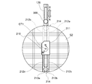
- FIG. 3 is a conceptual plan view showing a configuration of a resist coating apparatus having a small rotary arm according to the first embodiment. It is a top view which shows the movement range of the small rotation arm of the resist coating apparatus which concerns on the same Embodiment 1, Comprising: The case where a small rotation arm rotates about 180 degrees by a two-stage type is shown. It is a top view which shows the movement range of the small rotation arm of the resist coating apparatus which concerns on a comparative example, Comprising: The case where a small rotation arm rotates 360 degrees by a one-stage type is shown.
- FIG. 3 is a plan view showing a transfer robot of the resist coating apparatus according to the first embodiment. It is a top view which shows the semiconductor manufacturing apparatus which concerns on a comparative example.
- a large-diameter semiconductor wafer (not shown) is transferred between the apparatus front chamber 65 and the processing chamber 67 (loading and unloading).
- an articulated horizontal transfer robot 70 It is common to use an articulated horizontal transfer robot 70.
- reference numeral “61” is a cassette opener
- reference numeral “62” is a cassette
- reference numeral “63” is a load lock chamber
- reference numeral “64” is a traveling conveyance device
- reference numeral “66” is a transfer chamber.
- FIG. 1, FIG. 2, FIG. 3A, FIG. 4A and FIG. 4B show Embodiment 1 of the present invention.
- the semiconductor manufacturing apparatus 100 is provided adjacent to the apparatus front chamber 120 and the apparatus front chamber 120, and is connected to the apparatus front chamber 120 via the transfer port 130.
- a resist coating apparatus 110 as a processing chamber for transferring a semiconductor wafer (processing substrate) 300 between the two.
- the apparatus front chamber 120 and the resist coating apparatus 110 are configured to be separable from each other.
- the apparatus front chamber 120 is a room for taking out the semiconductor wafer 300 accommodated in a wafer transfer container (not shown) and transferring it to the resist coating apparatus 110.
- the apparatus front chamber 120 has a housing 125 having a box shape (in the first embodiment, a vertically long rectangular parallelepiped).
- the top plate 125 a of the housing 125 presses and fixes the container mounting table 121 for mounting the wafer transfer container and the wafer transfer container mounted on the container mounting table 121 from above.
- a holding lever 122 and operation buttons 124 for operating the semiconductor manufacturing apparatus 100 are provided. Further, in the housing 125, as shown in FIG.
- an extendable arm 126 for carrying the semiconductor wafer 300 taken out from the wafer transfer container downward into the resist coating device 110 via the transfer port 130 is provided in the horizontal direction. It is supported so that it can expand and contract in the directions of arrows A and B.
- a substrate mounting portion 126 a is formed at the tip of the extendable arm 126.
- the resist coating apparatus 110 receives the semiconductor wafer 300 from the apparatus front chamber 120 via the transfer port 130 and performs a known resist film forming process on the semiconductor wafer 300.
- a semiconductor wafer 300 having a small diameter of 20 mm or less (for example, 12.5 ⁇ 0.2 mm) is used.
- the resist coating apparatus 110 has a housing 111 in one small box shape (in the first embodiment, a rectangular parallelepiped having a length of 30 cm, a width of 30 cm, and a height of 26 cm). In the housing 111, as shown in FIG.
- a transfer robot 210 is installed in the vicinity of the transfer port 130, and a plurality of substrate processing apparatuses, that is, a HMDS (hexamethyldisilazane) processing unit 220, a coater cup.
- the unit 230, the resist nozzle 240, the EBR (Edge Bead Removal) nozzle 250, the bake processing unit 260, and the like are installed so as to surround the transfer robot 210.
- the transfer robot 210 receives the semiconductor wafer 300 from the telescopic arm 126 of the front chamber 120 and sequentially transfers the semiconductor wafer 300 to the HMDS processing unit 220, the coater unit 230, and the bake processing unit 260.
- the transfer robot 210 has a base 215. On the upper side of the base 215, there are two-stage movements (that is, both rotational and forward / backward movements). A small rotating arm 211 of a possible method) is provided at the top of the transfer robot 210.
- the small rotary arm 211 has the rotation center CT1 on the side close to the transport port 130 (upper side in FIG. 2) and the substrate holding part on the side farther from the transport port 130 (lower side in FIG. 2).
- 214 and as shown in FIG. 3A, in a direction of arrows M and N around the rotation center CT1, a first angular position P2, a second angular position P3, and a third angle in a direction of arrows M and N. It is configured to be able to rotate about 180 ° to the position P4.
- the reference angular position P ⁇ b> 1 is an angular position in which the substrate holding part 214 of the small rotary arm 211 is directed in the opposite direction to the apparatus front chamber 120.
- the first angular position P ⁇ b> 2 is an angular position at which the substrate holder 214 of the small rotary arm 211 faces the HMDS processing unit 220.
- the second angular position P3 is an angular position at which the substrate holding part 214 of the small rotary arm 211 faces the coater cup part 230.
- the third angular position P4 is an angular position that faces the bake processing unit 260.
- the second angular position P3 coincides with the reference angular position P1.
- the first angular position P2 is about 90 ° away from the second angular position P3 in the arrow N direction.
- the third angular position P4 is about 90 ° away from the second angular position P3 in the direction of the arrow M.
- the small rotary arm 211 is configured so as to be able to advance and retreat in the directions of arrows C and D which are horizontal directions, and the rotation center CT1 is centered on the base 215.
- the arm main body 217 is supported so as to be rotatable about 180 ° in the directions of arrows M and N, and protrudes laterally (in the direction of arrow C) from the arm main body 217 in a horizontal direction perpendicular to the protruding direction (in the direction of arrow C)
- a pair of hand portions 212a and 212b are supported by an air cylinder 219 so that they can be opened and closed synchronously in the directions of arrows E and F. As shown in FIGS.
- each of the hand portions 212a and 212b includes a hand main body 216a and 216b arranged in parallel with each other, and an arc-shaped substrate mounted on a position higher than the hand main bodies 216a and 216b. It has placement parts 213a and 213b.
- a substrate holding unit 214 is formed by the pair of substrate mounting units 213a and 213b.
- the small rotary arm 211 has a hand for finely adjusting a distance L1 between the pair of hand portions 212a and 212b when fully closed (when the semiconductor wafer 300 is placed).
- a part centering adjustment mechanism 270 is provided.
- the hand part centering adjustment mechanism 270 includes a first female screw part 271, a stopper 272, a set screw 273, a second female screw part 275, a lock nut 276, and the like.
- the first female screw portion 271 is formed in the hand body 216b of one hand portion 212b so as to penetrate in the direction parallel to the directions of arrows E and F.
- a bolt-shaped stopper 272 is screwed into the female screw portion 271.
- a second female threaded portion 275 is formed in the hand main body 216a of the other hand portion 212a so as to face the first female threaded portion 271 in a direction parallel to the arrow E and F directions.
- a set screw 273 having a long screw bolt shape is screwed into the 2 female thread portion 275.
- a lock nut 276 is screwed into the set screw 273.
- the HMDS processing unit 220 is a mechanism for performing HMDS processing (that is, processing for replacing the OH group (hydroxyl group) on the surface of the semiconductor wafer 300 with HMDS in order to improve the adhesion between the photoresist and the semiconductor wafer 300). It is. As shown in FIG. 2, the HMDS processing unit 220 includes a hot plate 221 and an elevating device 223. Further, the elevating device 223 includes four elevating pin members 222a to 222d.
- the coater cup unit 230 is a mechanism for performing formation of a resist film on the semiconductor wafer 300, EBR processing, back surface cleaning processing, and the like. As shown in FIG. 2, the coater cup unit 230 includes a turntable 231 for holding and rotating the semiconductor wafer 300.
- the resist nozzle 240 is a nozzle for supplying a photoresist solution to the semiconductor wafer 300 rotating on the turntable 231 of the coater cup unit 230 in the resist film forming process.
- the nozzle port 241 is rotated to the upper part of the center of the semiconductor wafer 300 placed on the turntable 231 of the coater cup unit 230, and the semiconductor wafer 300 is moved. A photoresist solution is dropped on the top.
- the EBR nozzle 250 is a nozzle for supplying a resist solution to the peripheral portion of the semiconductor wafer 300 in an EBR step (that is, a step of removing the resist film formed on the peripheral portion of the semiconductor wafer 300).
- an EBR step that is, a step of removing the resist film formed on the peripheral portion of the semiconductor wafer 300.
- the baking processing unit 260 is a mechanism for heating the semiconductor wafer 300 in order to solidify the photoresist film. As shown in FIG. 2, the bake processing unit 260 includes a hot plate 261 and an elevating device 263. Further, the elevating device 263 includes four elevating and lowering pin members 262a to 262d.
- HMDS processing unit 220 coater cup unit 230, resist nozzle 240, EBR nozzle 250, bake processing unit 260, etc.
- HMDS processing unit 220 coater cup unit 230, resist nozzle 240, EBR nozzle 250, bake processing unit 260, etc.
- the semiconductor manufacturing apparatus 100 has the same small transport robot 210 and a plurality of substrate processing apparatuses (HMDS processing unit 220, coater cup unit 230, resist nozzle 240, EBR nozzle 250, bake processing unit 260, etc.). Since it is installed in the housing 111, the resist coating apparatus 110 can be reduced in size and price. As a result, the entire semiconductor manufacturing apparatus 100 can be reduced in size and price, and a semiconductor chip can be manufactured at a low cost using the semiconductor wafer 300 having a small diameter.
- substrate processing apparatuses HMDS processing unit 220, coater cup unit 230, resist nozzle 240, EBR nozzle 250, bake processing unit 260, etc.
- the small rotation arm 211 is provided with the hand centering adjustment mechanism 270, and the distance L1 between the pair of hands 212a and 212b when fully closed can be easily finely adjusted. It is possible to suppress the eccentricity of the semiconductor wafer 300 by performing the alignment of the semiconductor wafer 300 on the small rotating arm 211.
- the semiconductor wafer 300 is carried from the front chamber 120 to the resist coating apparatus 110.
- the small rotary arm 211 of the transfer robot 210 is retracted in the arrow D direction and is positioned at the reference angular position P1.
- the extendable arm 126 is extended along with the semiconductor wafer 300 in the direction of arrow A.
- the telescopic arm 126 After the telescopic arm 126 enters the housing 111 of the resist coating apparatus 110 through the transport port 130, the telescopic arm 126 straddles over the transport robot 210 and does not contact the small rotating arm 211 (see FIG. 2). Proceed downward (to the right of FIGS. 4A and 4B). Therefore, the semiconductor wafer 300 is transferred from the substrate mounting portion 126 a of the extendable arm 126 to the substrate holding portion 214 of the small rotary arm 211.
- a specific method for delivering the semiconductor wafer 300 from the substrate mounting portion 126a of the extendable arm 126 to the substrate holding portion 214 of the small rotary arm 211 is as follows. That is, the telescopic arm 126 advances in the direction of arrow A above the area between the transfer robot 210 and the hand main bodies 216a and 216b, so that the semiconductor wafer 300 becomes a small rotating arm as shown by imaginary lines in FIGS. 4A and 4B. When reaching the substrate holding part 214 of 211, the telescopic arm 126 passes between the substrate mounting parts 213a and 213b of the hand main bodies 216a and 216b and is lowered.
- the semiconductor wafer 300 moves from the substrate mounting portion 126 a of the extendable arm 126 to the substrate holding portion 214 of the small rotation arm 211. Thereafter, the telescopic arm 126 is contracted in the arrow B direction. As a result, the semiconductor wafer 300 is transferred from the substrate mounting portion 126 a of the extendable arm 126 to the substrate holding portion 214 of the small rotary arm 211.
- the substrate holding part 214 is formed at a position higher than the hand main bodies 216a and 216b. Therefore, even if the telescopic arm 126 is lowered and contracted, the telescopic arm 126 remains in the hand main body 216a. Therefore, there is no possibility of interfering with 216b, so that the operation of transferring the semiconductor wafer 300 from the substrate mounting portion 126a of the extendable arm 126 to the substrate holding portion 214 of the small rotary arm 211 can be easily performed.
- the transfer robot 210 transfers the semiconductor wafer 300 to the HMDS processing unit 220.
- the small rotating arm 211 is rotated about 90 ° in the direction of the arrow N while being retracted in the direction of the arrow D, and is positioned at the first angular position P2, as indicated by an imaginary line in FIG.
- the arm 211 is moved forward in the direction of arrow C toward the HMDS processing unit 220.
- the semiconductor wafer 300 reaches directly above the lifting device 223 of the HMDS processing unit 220, the small rotating arm 211 is stopped, and the semiconductor wafer 300 is transferred from the small rotating arm 211 to the HMDS processing unit 220.
- a specific method for delivering the semiconductor wafer 300 from the small rotary arm 211 to the HMDS processing unit 220 is as follows. That is, in a state where the semiconductor wafer 300 has reached directly above the lifting device 223 of the HMDS processing unit 220, the four pin members 222a to 222d of the lifting device 223 are lifted to push up the semiconductor wafer 300 from below, so that the semiconductor wafer 300 is separated from the substrate holder 214 of the small rotary arm 211. Subsequently, after the hand portions 212 a and 212 b of the small rotating arm 211 are opened in the direction of arrow E, the four pin members 222 a to 222 d of the elevating device 223 are lowered to accommodate the semiconductor wafer 300 in the hot plate 221.
- the small rotary arm 211 is retracted in the direction of arrow D, and its hand portions 212a and 212b are closed in the direction of arrow F.
- the semiconductor wafer 300 is transferred from the small rotary arm 211 to the HMDS processing unit 220.
- the process proceeds to the third step, and the HMDS processing unit 220 performs HMDS processing on the semiconductor wafer 300.
- the process proceeds to the fourth step, and the semiconductor wafer 300 is transferred from the HMDS processing unit 220 to the coater cup unit 230 by the transfer robot 210 in the resist coating apparatus 110.
- the semiconductor wafer 300 is transferred from the HMDS processing unit 220 to the small rotary arm 211.
- the hand portions 212a and 212b of the small rotating arm 211 are opened in the direction of arrow E, and in this state, the small rotating arm 211 is advanced toward the HMDS processing unit 220 in the direction of arrow C.
- the small rotating arm 211 is stopped.
- the four pin members 222 a to 222 d of the elevating device 223 are raised, and the semiconductor wafer 300 is pushed up above the substrate holding part 214.
- the four pin members 222a to 222d of the lifting device 223 are lowered.
- the semiconductor wafer 300 is transferred from the HMDS processing unit 220 to the small rotary arm 211.
- the small rotary arm 211 is moved back in the direction of arrow D together with the semiconductor wafer 300, and then the small rotary arm 211 is rotated about 90 ° in the direction of arrow M while being moved back in the direction of arrow D.
- FIG. As shown by, the second angular position P3 is positioned.
- the small rotary arm 211 is advanced in the direction of arrow C toward the coater cup portion 230. Then, when the semiconductor wafer 300 reaches just above the turntable 231 of the coater cup unit 230, the small rotary arm 211 is stopped, and the spin chuck (not shown) of the coater cup unit 230 is moved up. Then, the semiconductor wafer 300 is held. Subsequently, after opening the hand portions 212a and 212b of the small rotary arm 211 in the direction of arrow E, the spin chuck is lowered. Thereafter, the small rotary arm 211 is retracted in the direction of arrow D, and its hand portions 212a and 212b are closed in the direction of arrow F. As a result, the semiconductor wafer 300 is transferred from the small rotary arm 211 to the coater cup unit 230.
- the process proceeds to the fifth step, and in the coater cup unit 230, the semiconductor wafer 300 is subjected to resist film formation, EBR processing, back surface cleaning processing, and the like using the resist nozzle 240 and the EBR nozzle 250.
- the process proceeds to the sixth step, and the semiconductor wafer 300 is transferred from the coater cup unit 230 to the bake processing unit 260 by the transfer robot 210 in the resist coating apparatus 110.
- the semiconductor wafer 300 is transferred from the coater cup unit 230 to the small rotary arm 211.
- the hand portions 212a and 212b of the small rotating arm 211 are opened in the direction of arrow E, and the small rotating arm 211 is moved forward in the direction of arrow C toward the coater cup portion 230.
- the small rotating arm 211 is stopped, and the spin chuck (not shown) of the coater cup part 230 is removed. Raise to above the substrate holder 214.
- the hand portions 212a and 212b of the small rotary arm 211 are closed in the arrow F direction.
- the spin chuck is lowered, and the semiconductor wafer 300 is held by the substrate holder 214 of the small rotary arm 211.
- the semiconductor wafer 300 is transferred from the coater cup unit 230 to the small rotary arm 211.
- the small rotary arm 211 is moved back in the direction of arrow D together with the semiconductor wafer 300, and then the small rotary arm 211 is rotated about 90 ° in the direction of arrow M while being moved back in the direction of arrow D.
- the small rotating arm 211 is advanced in the direction of arrow C toward the baking unit 260.
- the small rotary arm 211 is stopped, and the semiconductor wafer 300 is transferred from the small rotary arm 211 to the bake processing unit 260.
- a specific method for delivering the semiconductor wafer 300 from the small rotating arm 211 to the bake processing unit 260 is as follows. That is, in a state where the semiconductor wafer 300 has reached directly above the lifting device 263 of the bake processing unit 260, the four pin members 262a to 262d of the lifting device 263 are lifted to push up the semiconductor wafer 300 from below, thereby causing the semiconductor wafer 300 to rise. 300 is separated from the substrate holder 214 of the small rotary arm 211. Subsequently, after the hand portions 212a and 212b of the small rotating arm 211 are opened in the direction of arrow E, the four pin members 262a to 262d of the lifting device 223 are lowered and the semiconductor wafer 300 is accommodated in the hot plate 261.
- the small rotary arm 211 is retracted in the direction of arrow D, and its hand portions 212a and 212b are closed in the direction of arrow F.
- the semiconductor wafer 300 is transferred from the small rotary arm 211 to the bake processing unit 260.
- the process proceeds to the seventh step, where the baking processing unit 260 heats the semiconductor wafer 300 on the hot plate 261 in order to solidify the photoresist film.
- the process proceeds to the eighth step, and the semiconductor wafer 300 is returned to the transfer robot 210.
- the semiconductor wafer 300 is transferred from the bake processing unit 260 to the small rotary arm 211.
- the hand portions 212a and 212b of the small rotating arm 211 are opened in the direction of arrow E, and in this state, the small rotating arm 211 is advanced toward the baking unit 260 in the direction of arrow C.
- the small rotating arm 211 is stopped.
- the four pin members 262 a to 262 d of the elevating device 263 are raised to push the semiconductor wafer 300 up from above to above the substrate holding part 214.
- the hand portions 212a and 212b of the small rotary arm 211 are closed in the direction of arrow F, and then the four pin members 262a to 262d of the lifting device 263 are lowered.
- the semiconductor wafer 300 is transferred from the bake processing unit 260 to the small rotary arm 211.
- the small rotating arm 211 is moved back in the direction of arrow D together with the semiconductor wafer 300, and then the small rotating arm 211 is rotated about 90 ° in the direction of arrow N while being moved back in the direction of arrow D.
- the solid line in FIG. As shown, it is positioned at the reference angular position P1.
- the telescopic arm 126 of the apparatus front chamber 120 is extended in the arrow A direction. Then, after the telescopic arm 126 enters the housing 111 of the resist coating apparatus 110 from the transport port 130, the telescopic arm 126 straddles the front of the small robot arm 211 without touching the small rotating arm 211 so as to straddle the transport robot 210 (lower side in FIG. 2). 4A and 4B to the right). Therefore, the semiconductor wafer 300 is transferred from the substrate holding part 214 of the small rotary arm 211 to the substrate mounting part 126 a of the extendable arm 126.
- a specific method for delivering the semiconductor wafer 300 from the substrate holding part 214 of the small rotating arm 211 to the substrate mounting part 126a of the extendable arm 126 is as follows. That is, the telescopic arm 126 advances in the area between the hand main bodies 216 a and 216 b in the direction of arrow A, and when the substrate mounting portion 126 a reaches just below the semiconductor wafer 300, the telescopic arm 126 is moved to the small rotary arm 211. The substrate holding part 214 is raised so as to pass between the substrate placement parts 213a and 213b. Then, the semiconductor wafer 300 moves from the substrate holding part 214 of the small rotating arm 211 to the substrate mounting part 126a of the extendable arm 126.
- the telescopic arm 126 is contracted in the arrow B direction.
- the semiconductor wafer 300 is transferred from the substrate holding part 214 of the small rotary arm 211 to the substrate mounting part 126 a of the extendable arm 126.
- the substrate holding portion 214 is formed at a position higher than the hand main bodies 216a and 216b, the substrate mounting portion of the expansion / contraction arm 126 can be simply extended by extending the expansion / contraction arm 126 in the arrow A direction.
- 126 a can be inserted below the substrate holding unit 214, and thus the transfer operation of the semiconductor wafer 300 from the substrate holding unit 214 of the small rotation arm 211 to the substrate mounting unit 126 a of the extendable arm 126 can be easily performed. it can.
- the telescopic arm 126 is contracted together with the semiconductor wafer 300 in the direction of arrow B. Then, the telescopic arm 126 returns to the housing 125 of the apparatus front chamber 120 through the transfer port 130 without contacting the small rotary arm 211 so as to straddle the transfer robot 210.
- the semiconductor manufacturing apparatus 100 when the semiconductor wafer 300 is transported (carrying in and out) between the front chamber 120 and the resist coating apparatus 110, the telescopic arm 126 of the front chamber 120 is rotated in a small size. Since the semiconductor wafer 300 is transferred to the substrate holding part 214 of the small rotation arm 211 so as to extend without contacting the arm 211 and straddle the transfer robot 210, it is necessary to rotate the small rotation arm 211 in the housing 111. There is no. Therefore, in the resist coating apparatus 110, the occupation area of the transfer robot 210 in the horizontal plane can be reduced. As a result, the resist coating apparatus 110, and thus the entire semiconductor manufacturing apparatus 100, can be reduced in size and price, and the manufacturing cost of the semiconductor chip can be further reduced.
- the rotation angle of the small rotary arm 211 of the transfer robot 210 is about 180 °, and the small rotary arm 211 is a two-stage type, and the transfer robot in the resist coating apparatus 110.
- the small rotating arm 211 is used.
- the reference rotary position 211 By rotating the reference rotary position 211 from the reference angular position P1 to the first angular position P2, the second angular position P3, and the third angular position P4, and then moving the small rotary arm 211 forward toward the substrate processing apparatus.
- the delivery of the semiconductor wafer 300 can be executed.
- the occupation area in the horizontal plane of the transfer robot 210 can be significantly reduced as compared with the case where the small rotating arm 211 that rotates 360 ° in a single-stage type (cannot advance or retract) is provided. .
- the occupied area is a grid pattern area S2.
- the small rotating arm 211 of the transfer robot 210 rotates about 180 ° in a two-stage manner (that is, a method that can move in both the rotational direction and the forward / backward direction).
- the occupied area in the horizontal plane of the transfer robot 210 is a grid pattern area S1.
- the former is almost half of the latter because the rotation angle of the small rotary arm 211 is almost halved from 360 ° to about 180 °.
- the small rotary arm 211 is a two-stage type, the former is smaller than the latter depending on the degree of advancement and retreat.
- the semiconductor manufacturing apparatus 100 can significantly reduce the occupation area of the transfer robot 210 in the horizontal plane as compared with the case where the small rotation arm 211 that rotates 360 ° is a single-stage type (cannot advance and retract). .
- the semiconductor manufacturing apparatus using the semiconductor wafer 300 has been described.
- the present invention is applicable to other types of processing substrates (for example, insulating substrates such as a sapphire substrate, and conductive materials such as an aluminum substrate).
- a manufacturing apparatus for manufacturing a device from a non-disk-shaped (for example, rectangular) processing substrate for example, a non-disk-shaped (for example, rectangular) processing substrate.
- the housing 111 of the resist coating apparatus 110 is formed in a rectangular parallelepiped having a length of 30 cm, a width of 30 cm, and a height of 26 cm.
- the size (length, width, The height is not limited to this.
- the length is preferably 50 cm or less and 50 cm or less, more preferably 30 cm or less and 30 cm or less.
- the shape of the housing 111 is not limited to a rectangular parallelepiped, and may be formed in a cubic shape, a cylindrical shape, or other three-dimensional shapes, for example.
- the resist coating apparatus 110 including the HMDS processing unit 220, the coater cup unit 230, the resist nozzle 240, the EBR nozzle 250, the bake processing unit 260, and the like has been described as a plurality of substrate processing apparatuses. .
- the present invention can be similarly applied to a case where a device other than these devices (for example, a laser heating device) is provided as a substrate processing apparatus.
- the processing chamber is the resist coating apparatus 110
- the present invention may be similarly applied to a processing chamber other than the resist coating apparatus 110 (for example, a developing device). Is possible.
- the transfer robot 210 having the two-stage small rotary arm 211 has been described.
- the number of stages is three or more (in the forward and backward directions).
- a system in which two stages of moving mechanisms are provided may be used. It will be mentioned that as the number of stages of the small rotary arm 211 increases, the radius of rotation of the substrate holding unit 214 when the small rotary arm 211 is retracted is reduced, and the effect of narrowing the occupied area in the horizontal plane of the transfer robot 210 is increased. Nor.
- the present invention is applied to the semiconductor wafer 300 having a small diameter.
- the present invention is similarly applied to the semiconductor wafer 300 having a large diameter such as 8 inches or 12 inches. can do.
- the present invention is not limited to a manufacturing apparatus using a semiconductor wafer, but also other types of substrates (for example, an insulating substrate such as a sapphire substrate or a conductive substrate such as an aluminum substrate), or a non-disc shape (for example, a rectangular shape).
- substrates for example, an insulating substrate such as a sapphire substrate or a conductive substrate such as an aluminum substrate
- a non-disc shape for example, a rectangular shape.
- the present invention can also be applied to a manufacturing apparatus that manufactures a device from a processing substrate.
Landscapes
- Container, Conveyance, Adherence, Positioning, Of Wafer (AREA)
- Exposure Of Semiconductors, Excluding Electron Or Ion Beam Exposure (AREA)
Abstract
【課題】小口径の処理基板を用いる、小型で低コストの製造装置を提供する。 【解決手段】小型回転アームを最も上部に有する搬送ロボットと、この搬送ロボットを取り巻いて小型回転アームの回転円弧上に位置する複数の基板処理装置とが、1つのボックス形状のハウジング内に設置されている。小型回転アームへ処理基板が受け渡され、小型回転アームが回転中心を中心として回転することにより、各基板処理装置との間で処理基板の受け渡しを行う。これにより、製造装置を小型化および低価格化することができる。
Description
本発明は、小型回転アームを有する処理室および小型製造装置に関し、例えば、直径が20mm以下の小口径の半導体ウェハ等の処理基板に対して、レジストの塗布、露光、現像、エッチング加工など各種の処理(プロセス)を各基板処理装置で実施可能な小型回転アームを有する処理室と、この処理室を備えた半導体製造装置とに関するものである。
従来、半導体製造技術では、半導体ウェハの大口径化(例えば、直径8インチ、12インチ等)によって、チップ製造単価の低減が図られてきた。このため、一連の製造プロセスで使用される装置は巨大化および高価格化の一途をたどり、製造工場の規模や建設・運営コストを肥大化させることとなった。このような大規模製造システムは、少品種大量生産ではチップの製造単価の低減には寄与するものの、少量多品種生産の要請に応えにくく、市場状況に応じた生産量の調整を困難にすると共に、中小企業の参入を困難にしている。これらの問題を解決するためには、小口径の半導体ウェハを用いて低コストで半導体チップを製造できる小型の半導体製造装置が望まれる。
上述したような大口径の半導体ウェハ向けの従来の半導体製造装置では、特許文献1に示されたように、多関節水平型の搬送ロボットを用いるのが一般的であった。
しかしながら、こうした多関節水平型の搬送ロボットは、そのアームの関節を曲げる分だけ、水平面内での占有面積(フットプリント)が広くなってしまう。そのため、処理室の小型化および低価格化の妨げとなり、ひいては半導体製造装置全体の小型化および低価格化の障害になる。したがって、小口径の半導体ウェハを用いて低コストで半導体チップを製造することができないという課題があった。
本発明は、このような事情に鑑み、小型化および低価格化を実現することが可能な小型回転アームを有する処理室を提供することを第1の目的とする。また、このような処理室を採用することにより、小型化および低価格化を実現することが可能な半導体製造装置を提供することを第2の目的とする。
本発明に係る小型回転アームを有する処理室は、装置前室に隣接して設けられ、搬送口を介して前記装置前室との間で処理基板の搬送を行う処理室であって、小型回転アームを最も上部に有する搬送ロボットと、この搬送ロボットを取り巻いて前記小型回転アームの回転円弧上に位置する複数の基板処理装置とが、1つのボックス形状のハウジング内に設置され、前記小型回転アームへ処理基板が受け渡され、前記小型回転アームが回転中心を中心として回転することにより、前記各基板処理装置との間で処理基板の受け渡しを行うように構成されているとしたことを特徴とする。
本発明において、前記小型回転アームは、前記搬送口に近い側に回転中心を有するとともに、前記搬送口から遠い側に基板保持部を有し、前記装置前室の伸縮アームが前記小型回転アームと接触することなく伸びて前記搬送ロボットの上を跨ぐようにして前記小型回転アームの前記基板保持部へ処理基板が受け渡されるように構成されることが望ましい。
本発明において、前記小型回転アームは、平行に配置された一対のハンド本体と、該ハンド本体にそれぞれ設けられた円弧状の基板載置部とを備え、前記装置前室の前記伸縮アームが、該一対のハンド本体の間の上方で伸びることによって、前記処理基板を前記基板保持部の上方まで移動させ、その後、該一対のハンド本体の間を通過するように該伸縮アームを下降させることで、該処理基板を該基板保持部に保持させることが望ましい。
本発明において、前記小型回転アームは、回転方向及び進退方向の両方に移動することが望ましい。
本発明に係る小型製造装置は、装置前室に隣接して設けられ、搬送口を介して前記装置前室との間で処理基板の搬送を行う処理室を備える小型製造装置であって、該処理室は、小型回転アームを最も上部に有する搬送ロボットと、この搬送ロボットを取り巻いて前記小型回転アームの回転円弧上に位置する複数の基板処理装置とが、1つのボックス形状のハウジング内に設置され、前記小型回転アームへ処理基板が受け渡され、前記小型回転アームが回転中心を中心として回転することにより、前記各基板処理装置との間で処理基板の受け渡しを行うように構成されていることを特徴とする。
本発明の処理室によれば、搬送ロボットおよび複数の基板処理装置が同一のハウジング内に設置されているので、処理室を小型化および低価格化することができる。その結果、製造装置全体をも小型化および低価格化することができ、小口径の処理基板を用いて低コストで基板処理を行うことが可能となる。
本発明の処理室において、装置前室と処理室との間で処理基板を搬送する際に、装置前室の伸縮アームが小型回転アームと接触することなく伸びて搬送ロボットの上を跨ぐようにして小型回転アームの基板保持部へ処理基板が受け渡される構成とすることにより、この受け渡し時にハウジング内で小型回転アームを回転させる必要がない。したがって、処理室において、搬送ロボットの水平面内での占有面積を狭くすることができる。その結果、処理室、ひいては半導体製造装置全体を小型化および低価格化することができ、半導体チップの製造コストを一層削減することが可能となる。
本発明の処理室において、平行に配置された一対のハンド本体の間を通過するように伸縮アームを下降させることにより、簡単な構成で、伸縮アームを小型回転アームと接触させることなしに、処理基板を基板保持部に保持させることができる。
本発明の処理室において、小型回転アームを回転方向及び進退方向の両方に移動可能なものとすることにより、小型回転アームを後退させた状態で所定の角度位置まで回転させた後、この小型回転アームを基板処理装置に向けて前進させることで、処理室内において搬送ロボットと各基板処理装置との間で処理基板の受け渡しを行うことができ、従って、搬送ロボットの水平面内での占有面積を大幅に狭くすることができる。その結果、処理室、ひいては半導体製造装置全体を小型化および低価格化することができ、基板処理のコストをますます削減することが可能となる。
本発明の小型製造装置によれば、製造装置全体を小型化および低価格化することができるので、小口径の半導体ウェハを用いて低コストで半導体チップを製造することが可能となる。
[比較例]
以下、比較例に係る半導体製造装置について、図5を用いて説明する。
以下、比較例に係る半導体製造装置について、図5を用いて説明する。
従来の大口径半導体ウェハ向けの従来の半導体製造装置では、図5に示すように、装置前室65と処理室67との間で大口径の半導体ウェハ(図示せず)を搬送(搬入および搬出)する際に、多関節水平型の搬送ロボット70を用いるのが一般的であった。なお、図5において、符号「61」はカセットオープナー、符号「62」はカセット、符号「63」はロードロック室、符号「64」は走行搬送装置、符号「66」はトランスファーチャンバーである。
しかしながら、こうした多関節水平型の搬送ロボット70は、そのアームの関節を曲げる分だけ、水平面内での占有面積(フットプリント)が広くなってしまう。そのため、処理室67の小型化および低価格化の妨げとなり、ひいては半導体製造装置全体の小型化および低価格化の障害になる。したがって、図5の半導体製造装置では、小口径の半導体ウェハを用いて低コストで半導体チップを製造することができない。
[発明の実施の形態1]
以下、本発明の実施の形態について説明する。
[発明の実施の形態1]
以下、本発明の実施の形態について説明する。
図1、図2、図3A、図4A及び図4Bに、本発明の実施の形態1を示す。
実施の形態1に係る半導体製造装置100は、図1、図2に示すように、装置前室120と、この装置前室120に隣接して設けられ、搬送口130を介して装置前室120との間で半導体ウェハ(処理基板)300の搬送を行う処理室としてのレジスト塗布装置110とを備えている。装置前室120とレジスト塗布装置110とは、互いに分離可能に構成されている。
装置前室120は、ウェハ搬送容器(図示せず)に収容された半導体ウェハ300を取り出して、レジスト塗布装置110に搬送するための部屋である。この装置前室120は、図1に示すように、1つのボックス形状(この実施の形態1では、縦長の直方体)のハウジング125を有している。ハウジング125の天板125aには、図1に示すように、ウェハ搬送容器を載置するための容器載置台121と、この容器載置台121に載置されたウェハ搬送容器を上方から押圧固定する押さえレバー122と、半導体製造装置100の操作を行うための操作ボタン124等が設けられている。また、ハウジング125内には、図2に示すように、ウェハ搬送容器から下方に取り出した半導体ウェハ300を搬送口130を経由してレジスト塗布装置110に搬入するための伸縮アーム126が、水平方向である矢印A、B方向に伸縮自在に支持されている。この伸縮アーム126の先端には、基板載置部126aが形成されている。
一方、レジスト塗布装置110は、図2に示すように、搬送口130を介して装置前室120から半導体ウェハ300を受け取り、この半導体ウェハ300に対して、公知のレジスト膜形成処理を行うためのものである。この実施の形態1では、半導体ウェハ300として、直径が20mm以下(例えば12.5±0.2mm)の小径のものを使用する。このレジスト塗布装置110は、図1に示すように、1つの小さなボックス形状(この実施の形態1では、縦30cm、横30cm、高さ26cmの直方体)のハウジング111を有している。ハウジング111内には、図2に示すように、搬送ロボット210が搬送口130の近傍に設置されているとともに、複数の基板処理装置、すなわち、HMDS(ヘキサメチルジシラザン)処理ユニット220、コーターカップ部230、レジストノズル240、EBR(Edge Bead Removal)ノズル250、ベーク処理ユニット260等が、搬送ロボット210を取り巻くように設置されている。
搬送ロボット210は、図2に示すように、半導体ウェハ300を装置前室120の伸縮アーム126から受け取って、HMDS処理ユニット220、コーター部230、ベーク処理ユニット260に順次搬送するためのものである。この搬送ロボット210は、図2、図4A及び図4Bに示すように、ベース215を有しており、ベース215の上側には、2段式(すなわち、回転方向及び進退方向の両方の移動が可能な方式)の小型回転アーム211が搬送ロボット210の最も上部に位置して設けられている。
すなわち、小型回転アーム211は、図2に示すように、搬送口130に近い側(図2上側)に回転中心CT1を有するとともに、搬送口130から遠い側(図2下側)に基板保持部214を有しており、図3Aに示すように、この回転中心CT1を中心として矢印M、N方向に、所定の基準角度位置P1から第1角度位置P2、第2角度位置P3、第3角度位置P4まで約180°回転しうるように構成されている。ここで、基準角度位置P1は、小型回転アーム211の基板保持部214が装置前室120とは正反対に向いた角度位置である。また、第1角度位置P2は、小型回転アーム211の基板保持部214がHMDS処理ユニット220に向き合う角度位置である。また、第2角度位置P3は、小型回転アーム211の基板保持部214がコーターカップ部230に向き合う角度位置である。さらに、第3角度位置P4は、ベーク処理ユニット260に向き合う角度位置である。なお、この実施の形態1では、第2角度位置P3は、基準角度位置P1に一致している。また、第1角度位置P2は、第2角度位置P3から矢印N方向に約90°離れている。さらに、第3角度位置P4は、第2角度位置P3から矢印M方向に約90°離れている。
また、小型回転アーム211は、図2、図4A及び図4Bに示すように、水平方向である矢印C、D方向に進退しうるように構成されており、ベース215上に回転中心CT1を中心として矢印M、N方向に約180°回転自在に支持されたアーム本体217と、このアーム本体217から横向き(矢印C方向)に突出され、この突出方向(矢印C方向)と直角な水平方向である矢印E、F方向にエアシリンダ219によって同期的に開閉自在に支持された一対のハンド部212a、212bとを備えている。各ハンド部212a、212bはそれぞれ、図4A及び図4Bに示すように、互いに平行に配置されたハンド本体216a、216bと、このハンド本体216a、216bより高い位置に形成された円弧状の基板載置部213a、213bとを有している。そして、これら一対の基板載置部213a、213bによって基板保持部214が形成されている。この基板保持部214に半導体ウェハ300が載置されるときは、半導体ウェハ300の外縁部が基板載置部212a、212bに接触するように載置される。
さらに、小型回転アーム211には、図4A及び図4Bに示すように、一対のハンド部212a、212b間の全閉時(半導体ウェハ300の載置時)の距離L1を微調整するためのハンド部センタリング調整機構270が設けられており、このハンド部センタリング調整機構270は、第1雌ねじ部271、ストッパ272、セットビス273、第2雌ねじ部275およびロックナット276等から構成されている。
すなわち、図4A及び図4Bに示すように、一方のハンド部212bのハンド本体216bには、第1雌ねじ部271が矢印E、F方向に平行な方向に貫通して形成されており、第1雌ねじ部271には、ボルト形状のストッパ272が螺合している。また、他方のハンド部212aのハンド本体216aには、第2雌ねじ部275が、第1雌ねじ部271に対向する形で矢印E、F方向に平行な方向に貫通して形成されており、第2雌ねじ部275には、長ねじボルト形状のセットビス273が螺合している。さらに、セットビス273にはロックナット276が螺合している。そのため、エアシリンダ219を駆動して一対のハンド部212a、212bを全閉にすると、図4Bに示すように、セットビス273の先端部がストッパ272の頭部に当たった状態で一対のハンド部212a、212bが停止する。したがって、セットビス273を所望の位置までねじ込んでロックナット276でハンド部212aに固定することにより、一対のハンド部212a、212b間の全閉時の距離L1を簡便に微調整することが可能となり、小型回転アーム211の利便性が向上する。
HMDS処理ユニット220は、HMDS処理(すなわち、フォトレジストと半導体ウェハ300との密着性を向上させるために、半導体ウェハ300表面のOH基(ヒドロキシル基)をHMDSで置換する処理)を行うための機構である。このHMDS処理ユニット220は、図2に示すように、ホットプレート221と昇降装置223とを備えている。さらに、昇降装置223は、4つの昇降自在のピン部材222a~222dを有している。
コーターカップ部230は、半導体ウェハ300に対するレジスト膜の形成や、EBR処理、裏面洗浄処理等を行うための機構である。このコーターカップ部230は、図2に示すように、半導体ウェハ300を保持して回転させるための回転台231を備えている。
レジストノズル240は、レジスト膜形成工程において、コーターカップ部230の回転台231上で回転する半導体ウェハ300にフォトレジスト液を供給するためのノズルである。このレジストノズル240を用いてフォトレジストを供給する際には、コーターカップ部230の回転台231に載置された半導体ウェハ300の中心部上方までノズル口241を回転移動させて、この半導体ウェハ300上にフォトレジスト液を滴下する。
EBRノズル250は、EBR工程(すなわち、半導体ウェハ300の周縁部に形成されたレジスト膜を除去する工程)において、半導体ウェハ300の周縁部にレジスト溶解液を供給するためのノズルである。このEBRノズル250を用いてレジスト膜を除去する際には、コーターカップ部230の回転台231に載置された半導体ウェハ300の周縁部上方までノズル口251を回転移動させて、この半導体ウェハ300上にレジスト溶液を滴下する。
ベーク処理ユニット260は、フォトレジスト膜を固化するために半導体ウェハ300を加熱するための機構である。このベーク処理ユニット260は、図2に示すように、ホットプレート261と昇降装置263とを備えている。さらに、昇降装置263は、4つの昇降自在のピン部材262a~262dを有している。
なお、上述した複数の基板処理装置(HMDS処理ユニット220、コーターカップ部230、レジストノズル240、EBRノズル250、ベーク処理ユニット260等)は、図2に示すように、いずれも搬送ロボット210の小型回転アーム211の回転円弧上に位置している。
以上説明したように、半導体製造装置100は、搬送ロボット210および複数の基板処理装置(HMDS処理ユニット220、コーターカップ部230、レジストノズル240、EBRノズル250、ベーク処理ユニット260等)が同一の小さなハウジング111内に設置されているので、レジスト塗布装置110を小型化および低価格化することができる。その結果、半導体製造装置100全体をも小型化および低価格化することができ、小口径の半導体ウェハ300を用いて低コストで半導体チップを製造することが可能となる。
また、小型回転アーム211には、上述したとおり、ハンド部センタリング調整機構270が設けられており、一対のハンド部212a、212b間の全閉時の距離L1を簡便に微調整することができるので、小型回転アーム211上で半導体ウェハ300の位置合わせを実行して半導体ウェハ300の偏心を抑制することが可能となる。
次に、この半導体製造装置100において、レジスト塗布装置110で半導体ウェハ300にレジストを塗布する動作について、図2~図4Bを用いて説明する。
まず、第1工程で、装置前室120からレジスト塗布装置110へ半導体ウェハ300を搬入する。このとき、図3Aに実線で示すように、搬送ロボット210の小型回転アーム211が矢印D方向に後退するとともに基準角度位置P1に位置決めされた状態である。そして、装置前室120の伸縮アーム126の基板載置部126aに半導体ウェハ300を載置した後、この伸縮アーム126を半導体ウェハ300とともに矢印A方向に伸ばす。すると、この伸縮アーム126は、搬送口130を経てレジスト塗布装置110のハウジング111内に侵入した後、搬送ロボット210の上を跨ぐようにして小型回転アーム211と接触することなく前方(図2の下方、図4A及び図4Bの右方)へ進む。そこで、半導体ウェハ300を伸縮アーム126の基板載置部126aから小型回転アーム211の基板保持部214に受け渡す。
なお、伸縮アーム126の基板載置部126aから小型回転アーム211の基板保持部214に半導体ウェハ300を受け渡す具体的な手法は、次のとおりである。すなわち、伸縮アーム126が搬送ロボット210、ハンド本体216a、216bの間の領域の上方を矢印A方向に前進して、図4A及び図4Bに想像線で示すように、半導体ウェハ300が小型回転アーム211の基板保持部214の真上に達したところで、伸縮アーム126をハンド本体216a、216bの基板載置部213a、213bの間を通過させて、下降させる。すると、伸縮アーム126の基板載置部126aから小型回転アーム211の基板保持部214に半導体ウェハ300が移動する。その後、伸縮アーム126を矢印B方向に縮める。これにより、半導体ウェハ300が伸縮アーム126の基板載置部126aから小型回転アーム211の基板保持部214に受け渡される。
このとき、基板保持部214は、図4Aに示すように、ハンド本体216a、216bより高い位置に形成されているので、伸縮アーム126を下降させて縮めても、この伸縮アーム126がハンド本体216a、216bに干渉する恐れはなく、したがって、伸縮アーム126の基板載置部126aから小型回転アーム211の基板保持部214への半導体ウェハ300の受け渡し動作を容易に実行することができる。
次に、第2工程に移行し、レジスト塗布装置110において、搬送ロボット210が、半導体ウェハ300をHMDS処理ユニット220へ搬送する。それには、小型回転アーム211を矢印D方向に後退させたまま矢印N方向に約90°回転させて、図3Aに想像線で示すように、第1角度位置P2に位置決めした後、この小型回転アーム211をHMDS処理ユニット220に向けて矢印C方向に前進させる。そして、半導体ウェハ300がHMDS処理ユニット220の昇降装置223の真上に達したところで、小型回転アーム211を停止させ、半導体ウェハ300を小型回転アーム211からHMDS処理ユニット220に受け渡す。
なお、小型回転アーム211からHMDS処理ユニット220に半導体ウェハ300を受け渡す具体的な手法は、次のとおりである。すなわち、半導体ウェハ300がHMDS処理ユニット220の昇降装置223の真上に達した状態で、昇降装置223の4つのピン部材222a~222dを上昇させて半導体ウェハ300を下から押し上げることにより、半導体ウェハ300を小型回転アーム211の基板保持部214から離間させる。続いて、小型回転アーム211のハンド部212a、212bを矢印E方向に開いた後、昇降装置223の4つのピン部材222a~222dを下降させて半導体ウェハ300をホットプレート221内に収容する。その後、小型回転アーム211を矢印D方向に後退させ、そのハンド部212a、212bを矢印F方向に閉じる。これにより、半導体ウェハ300が小型回転アーム211からHMDS処理ユニット220に受け渡される。
次いで、第3工程に移行し、HMDS処理ユニット220において、半導体ウェハ300に対してHMDS処理を行う。
次に、第4工程に移行し、レジスト塗布装置110において、搬送ロボット210により、半導体ウェハ300をHMDS処理ユニット220からコーターカップ部230へ搬送する。
それには、まず、半導体ウェハ300をHMDS処理ユニット220から小型回転アーム211に受け渡す。具体的には、小型回転アーム211のハンド部212a、212bを矢印E方向に開き、その状態で、小型回転アーム211をHMDS処理ユニット220に向けて矢印C方向に前進させる。そして、小型回転アーム211の基板保持部214が半導体ウェハ300の真上に達したところで、小型回転アーム211を停止させる。続いて、昇降装置223の4つのピン部材222a~222dを上昇させて、半導体ウェハ300を、基板保持部214の上方に押し上げる。その後、小型回転アーム211のハンド部212a、212bを矢印F方向に閉じた後、昇降装置223の4つのピン部材222a~222dを下降させる。これにより、半導体ウェハ300がHMDS処理ユニット220から小型回転アーム211に受け渡される。
その後、小型回転アーム211を半導体ウェハ300とともに矢印D方向に後退させた後、この小型回転アーム211を矢印D方向に後退させたまま矢印M方向に約90°回転させて、図3Aに想像線で示すように、第2角度位置P3に位置決めする。
続いて、この小型回転アーム211をコーターカップ部230に向けて矢印C方向に前進させる。そして、半導体ウェハ300がコーターカップ部230の回転台231の真上に達したところで、小型回転アーム211を停止させ、コーターカップ部230のスピンチャック(図示せず)を上昇させて、このスピンチャックで半導体ウェハ300を把持する。続いて、小型回転アーム211のハンド部212a、212bを矢印E方向に開いた後、このスピンチャックを下降させる。その後、小型回転アーム211を矢印D方向に後退させ、そのハンド部212a、212bを矢印F方向に閉じる。これにより、半導体ウェハ300が小型回転アーム211からコーターカップ部230に受け渡される。
次いで、第5工程に移行し、コーターカップ部230において、半導体ウェハ300に対して、レジストノズル240およびEBRノズル250を用いて、レジスト膜の形成、EBR処理、裏面洗浄処理等を行う。
次に、第6工程に移行し、レジスト塗布装置110において、搬送ロボット210により、半導体ウェハ300をコーターカップ部230からベーク処理ユニット260へ搬送する。
それには、まず、半導体ウェハ300をコーターカップ部230から小型回転アーム211に受け渡す。具体的には、小型回転アーム211のハンド部212a、212bを矢印E方向に開き、小型回転アーム211をコーターカップ部230に向けて矢印C方向に前進させる。そして、小型回転アーム211の基板保持部214がコーターカップ部230の回転台231の真上に達したところで、小型回転アーム211を停止させ、コーターカップ部230のスピンチャック(図示せず)を、基板保持部214の上方まで上昇させる。そして、小型回転アーム211のハンド部212a、212bを矢印F方向に閉じる。続いて、このスピンチャックを下降させて、小型回転アーム211の基板保持部214で半導体ウェハ300を保持する。これにより、半導体ウェハ300がコーターカップ部230から小型回転アーム211に受け渡される。
その後、小型回転アーム211を半導体ウェハ300とともに矢印D方向に後退させた後、この小型回転アーム211を矢印D方向に後退させたまま矢印M方向に約90°回転させて、図3Aに想像線で示すように、第3角度位置P4に位置決めする。
続いて、この小型回転アーム211をベーク処理ユニット260に向けて矢印C方向に前進させる。そして、半導体ウェハ300がベーク処理ユニット260の昇降装置263の真上に達したところで、小型回転アーム211を停止させ、半導体ウェハ300を小型回転アーム211からベーク処理ユニット260に受け渡す。
なお、小型回転アーム211からベーク処理ユニット260に半導体ウェハ300を受け渡す具体的な手法は、次のとおりである。すなわち、半導体ウェハ300がベーク処理ユニット260の昇降装置263の真上に達した状態で、昇降装置263の4つのピン部材262a~262dを上昇させて半導体ウェハ300を下から押し上げることにより、半導体ウェハ300を小型回転アーム211の基板保持部214から離間させる。続いて、小型回転アーム211のハンド部212a、212bを矢印E方向に開いた後、昇降装置223の4つのピン部材262a~262dを下降させて半導体ウェハ300をホットプレート261内に収容する。その後、小型回転アーム211を矢印D方向に後退させ、そのハンド部212a、212bを矢印F方向に閉じる。これにより、半導体ウェハ300が小型回転アーム211からベーク処理ユニット260に受け渡される。
次いで、第7工程に移行し、ベーク処理ユニット260において、ホットプレート261上の半導体ウェハ300に対して、フォトレジスト膜を固化するために加熱する。
次に、第8工程に移行し、半導体ウェハ300を搬送ロボット210に戻す。
それには、まず、半導体ウェハ300をベーク処理ユニット260から小型回転アーム211に受け渡す。具体的には、小型回転アーム211のハンド部212a、212bを矢印E方向に開き、その状態で、小型回転アーム211をベーク処理ユニット260に向けて矢印C方向に前進させる。そして、小型回転アーム211の基板保持部214が半導体ウェハ300の真上に達したところで、小型回転アーム211を停止させる。続いて、昇降装置263の4つのピン部材262a~262dを上昇させて半導体ウェハ300を、下から、基板保持部214の上方まで押し上げる。その後、小型回転アーム211のハンド部212a、212bを矢印F方向に閉じた後、昇降装置263の4つのピン部材262a~262dを下降させる。これにより、半導体ウェハ300がベーク処理ユニット260から小型回転アーム211に受け渡される。
その後、小型回転アーム211を半導体ウェハ300とともに矢印D方向に後退させた後、この小型回転アーム211を矢印D方向に後退させたまま矢印N方向に約90°回転させて、図3Aに実線で示すように、基準角度位置P1に位置決めする。
最後に、第9工程に移行し、レジスト塗布装置110から装置前室120へ半導体ウェハ300を搬出する。
それには、まず、装置前室120の伸縮アーム126を矢印A方向に伸ばす。すると、この伸縮アーム126は、搬送口130からレジスト塗布装置110のハウジング111内に侵入した後、搬送ロボット210の上を跨ぐようにして小型回転アーム211と接触することなく前方(図2の下方、図4A及び図4Bの右方)へ進む。そこで、半導体ウェハ300を小型回転アーム211の基板保持部214から伸縮アーム126の基板載置部126aに受け渡す。
なお、小型回転アーム211の基板保持部214から伸縮アーム126の基板載置部126aに半導体ウェハ300を受け渡す具体的な手法は、次のとおりである。すなわち、伸縮アーム126がハンド本体216a、216bの間の領域を矢印A方向に前進して、その基板載置部126aが半導体ウェハ300の真下に達したところで、伸縮アーム126を小型回転アーム211の基板保持部214の基板載置部213a、213bの間を通過するように、上昇させる。すると、小型回転アーム211の基板保持部214から伸縮アーム126の基板載置部126aに半導体ウェハ300が移動する。その後、伸縮アーム126を矢印B方向に縮める。これにより、半導体ウェハ300が小型回転アーム211の基板保持部214から伸縮アーム126の基板載置部126aに受け渡される。
このとき、基板保持部214は、図4Aに示すように、ハンド本体216a、216bより高い位置に形成されているので、伸縮アーム126を矢印A方向に伸ばすだけで伸縮アーム126の基板載置部126aを基板保持部214の下方に差し込むことができ、したがって、小型回転アーム211の基板保持部214から伸縮アーム126の基板載置部126aへの半導体ウェハ300の受け渡し動作を容易に実行することができる。
その後、伸縮アーム126を半導体ウェハ300とともに矢印B方向に縮める。すると、この伸縮アーム126は、搬送ロボット210の上を跨ぐようにして小型回転アーム211と接触することなく搬送口130を経て装置前室120のハウジング125に戻る。
ここで、レジスト塗布装置110において半導体ウェハ300にレジストを塗布する動作が終了する。
このように、この半導体製造装置100において、装置前室120とレジスト塗布装置110との間で半導体ウェハ300を搬送(搬入および搬出)する際には、装置前室120の伸縮アーム126が小型回転アーム211と接触することなく伸びて搬送ロボット210の上を跨ぐようにして小型回転アーム211の基板保持部214へ半導体ウェハ300が受け渡されるため、ハウジング111内で小型回転アーム211を回転させる必要がない。したがって、レジスト塗布装置110において、搬送ロボット210の水平面内での占有面積を狭くすることができる。その結果、レジスト塗布装置110、ひいては半導体製造装置100全体を小型化および低価格化することができ、半導体チップの製造コストを一層削減することが可能となる。
また、この半導体製造装置100においては、搬送ロボット210の小型回転アーム211の回転角度が約180°であるとともに、この小型回転アーム211が2段式であって、レジスト塗布装置110内において搬送ロボット210と各基板処理装置(HMDS処理ユニット220、コーターカップ部230、レジストノズル240、EBRノズル250、ベーク処理ユニット260等)との間で半導体ウェハ300の受け渡しを行う際には、小型回転アーム211を後退させた状態で基準角度位置P1から第1角度位置P2、第2角度位置P3、第3角度位置P4まで回転させた後、この小型回転アーム211を基板処理装置に向けて前進させることにより、この半導体ウェハ300の受け渡しを実行することができる。その結果、以下に説明するとおり、1段式(進退不可)で360°回転する小型回転アーム211を有する場合と比べて、搬送ロボット210の水平面内での占有面積を大幅に狭くすることができる。
すなわち、搬送ロボット210の小型回転アーム211が1段式(すなわち、回転はできるが、進退はできない方式)で360°回転すると仮定すると、図3Bに示すように、搬送ロボット210の水平面内での占有領域は、格子模様の領域S2になる。これに対して、この実施の形態1のように、搬送ロボット210の小型回転アーム211が2段式(すなわち、回転方向及び進退方向の両方の移動が可能な方式)で約180°回転する場合には、図3Aに示すように、搬送ロボット210の水平面内での占有領域は、格子模様の領域S1になる。ここで、領域S1、S2の面積を比較すると、まず、小型回転アーム211の回転角度が360°から約180°にほぼ半減したことにより、前者は後者のほぼ半分になる。これに加えて、小型回転アーム211が2段式であれば、その進退の程度に応じて前者は後者より小さくなる。例えば、小型回転アーム211の基板保持部214の回転半径が、小型回転アーム211を後退させることによって半分(1/2)になるとすると、小型回転アーム211が回転時に掃く面積(小型回転アーム211の回転中心CT1から基板保持部214までの距離を半径とする円の面積)は、基板保持部214の回転半径の2乗に比例することから、1/4になる。したがって、この半導体製造装置100は、1段式(進退不可)で360°回転する小型回転アーム211を有する場合と比べて、搬送ロボット210の水平面内での占有面積を大幅に狭くすることができる。
その結果、レジスト塗布装置110、ひいては半導体製造装置100全体を小型化および低価格化することができ、半導体チップの製造コストをますます削減することが可能となる。
[発明のその他の実施の形態]
なお、上述した実施の形態1では、半導体ウェハ300を用いる半導体製造装置について説明したが、本発明は、他の種類の処理基板(例えば、サファイア基板等の絶縁性基板や、アルミニウム基板等の導電性基板)や、非円盤形状(例えば、矩形)の処理基板からデバイスを製造する製造装置にも適用することができる。
なお、上述した実施の形態1では、半導体ウェハ300を用いる半導体製造装置について説明したが、本発明は、他の種類の処理基板(例えば、サファイア基板等の絶縁性基板や、アルミニウム基板等の導電性基板)や、非円盤形状(例えば、矩形)の処理基板からデバイスを製造する製造装置にも適用することができる。
また、上述した実施の形態1では、レジスト塗布装置110のハウジング111が縦30cm、横30cm、高さ26cmの直方体に形成されている場合について説明したが、このハウジング111のサイズ(縦、横、高さ)は、これに限るわけではない。ただし、レジスト塗布装置110を小型化および低価格化する観点からは、縦50cm以下、横50cm以下が好ましく、縦30cm以下、横30cm以下がさらに好ましい。また、このハウジング111の形状は直方体に限るわけではなく、例えば、立方体、円筒状その他の立体形状に形成しても構わない。
また、上述した実施の形態1では、複数の基板処理装置として、HMDS処理ユニット220、コーターカップ部230、レジストノズル240、EBRノズル250、ベーク処理ユニット260等を備えたレジスト塗布装置110について説明した。しかし、これら以外の装置・機器(例えば、レーザ加熱装置など)を基板処理装置として備えている場合にも本発明を同様に適用することができる。
また、上述した実施の形態1では、処理室がレジスト塗布装置110である場合について説明したが、レジスト塗布装置110以外の処理室(例えば、現像装置など)に本発明を同様に適用することも可能である。
また、上述した実施の形態1では、2段式の小型回転アーム211を有する搬送ロボット210について説明したが、この小型回転アーム211の段数は、1段であっても3段以上(進退方向に移動する機構を2段設けた方式)であっても構わない。小型回転アーム211の段数が増えるほど、小型回転アーム211の後退時の基板保持部214の回転半径が小さくなり、搬送ロボット210の水平面内での占有面積を狭くする効果が高まることは言及するまでもない。
さらに、上述した実施の形態1では、本発明を小口径の半導体ウェハ300に適用した場合について説明したが、8インチや12インチ等の大口径の半導体ウェハ300等にも本発明を同様に適用することができる。
また、本発明は、半導体ウェハを用いる製造装置だけでなく、他の種類の基板(例えばサファイア基板等の絶縁性基板や、アルミニウム基板等の導電性基板)や、非円盤形状(例えば矩形)の処理基板からデバイスを製造する製造装置にも適用することができる。
100……半導体製造装置
110……レジスト塗布装置(処理室)
111……ハウジング
120……装置前室
125……ハウジング
126……伸縮アーム
130……搬送口
210……搬送ロボット
211……小型回転アーム
214……基板保持部
220……HMDS処理ユニット(基板処理装置)
230……コーターカップ部(基板処理装置)
240……レジストノズル(基板処理装置)
250……EBRノズル(基板処理装置)
260……ベーク処理ユニット(基板処理装置)
300……半導体ウェハ(処理基板)
CT1……小型回転アームの回転中心
110……レジスト塗布装置(処理室)
111……ハウジング
120……装置前室
125……ハウジング
126……伸縮アーム
130……搬送口
210……搬送ロボット
211……小型回転アーム
214……基板保持部
220……HMDS処理ユニット(基板処理装置)
230……コーターカップ部(基板処理装置)
240……レジストノズル(基板処理装置)
250……EBRノズル(基板処理装置)
260……ベーク処理ユニット(基板処理装置)
300……半導体ウェハ(処理基板)
CT1……小型回転アームの回転中心
Claims (5)
- 装置前室に隣接して設けられ、搬送口を介して前記装置前室との間で処理基板の搬送を行う処理室であって、
小型回転アームを最も上部に有する搬送ロボットと、この搬送ロボットを取り巻いて前記小型回転アームの回転円弧上に位置する複数の基板処理装置とが、1つのボックス形状のハウジング内に設置され、前記小型回転アームへ処理基板が受け渡され、前記小型回転アームが回転中心を中心として回転することにより、前記各基板処理装置との間で処理基板の受け渡しを行うように構成されていることを特徴とする小型回転アームを有する処理室。 - 前記小型回転アームは、前記搬送口に近い側に回転中心を有するとともに、前記搬送口から遠い側に基板保持部を有し、前記装置前室の伸縮アームが前記小型回転アームと接触することなく伸びて前記搬送ロボットの上を跨ぐようにして前記小型回転アームの前記基板保持部へ処理基板が受け渡されるように構成されていることを特徴とする請求項1に記載の小型回転アームを有する処理室。
- 前記小型回転アームは、平行に配置された一対のハンド本体と、該ハンド本体にそれぞれ設けられた円弧状の基板載置部とを備え、
前記装置前室の前記伸縮アームが、該一対のハンド本体の間の上方で伸びることによって、前記処理基板を前記基板保持部の上方まで移動させ、その後、該一対の基板載置部の間を通過するように該伸縮アームを下降させることで、該処理基板を該基板保持部に保持させる、
ことを特徴とする請求項2に記載の処理室。 - 前記小型回転アームが、回転方向及び進退方向の両方に移動することを特徴とする請求項1に記載の小型回転アームを有する処理室。
- 装置前室に隣接して設けられ、搬送口を介して前記装置前室との間で処理基板の搬送を行う処理室を備える小型製造装置であって、
該処理室は、
小型回転アームを最も上部に有する搬送ロボットと、この搬送ロボットを取り巻いて前記小型回転アームの回転円弧上に位置する複数の基板処理装置とが、1つのボックス形状のハウジング内に設置され、前記小型回転アームへ処理基板が受け渡され、前記小型回転アームが回転中心を中心として回転することにより、前記各基板処理装置との間で処理基板の受け渡しを行うように構成されていることを特徴とする小型製造装置。
Priority Applications (1)
| Application Number | Priority Date | Filing Date | Title |
|---|---|---|---|
| JP2015549221A JP6404828B2 (ja) | 2013-11-25 | 2014-11-25 | 小型回転アームを有する処理室および小型製造装置 |
Applications Claiming Priority (2)
| Application Number | Priority Date | Filing Date | Title |
|---|---|---|---|
| JP2013-242497 | 2013-11-25 | ||
| JP2013242497 | 2013-11-25 |
Publications (1)
| Publication Number | Publication Date |
|---|---|
| WO2015076405A1 true WO2015076405A1 (ja) | 2015-05-28 |
Family
ID=53179664
Family Applications (1)
| Application Number | Title | Priority Date | Filing Date |
|---|---|---|---|
| PCT/JP2014/081050 Ceased WO2015076405A1 (ja) | 2013-11-25 | 2014-11-25 | 小型回転アームを有する処理室および小型製造装置 |
Country Status (2)
| Country | Link |
|---|---|
| JP (1) | JP6404828B2 (ja) |
| WO (1) | WO2015076405A1 (ja) |
Cited By (1)
| Publication number | Priority date | Publication date | Assignee | Title |
|---|---|---|---|---|
| US20210213614A1 (en) * | 2018-05-11 | 2021-07-15 | Kawasaki Jukogyo Kabushiki Kaisha | Substrate transfer robot and method of detecting optical-axis deviation of substrate hold hand |
Citations (3)
| Publication number | Priority date | Publication date | Assignee | Title |
|---|---|---|---|---|
| JP2000150610A (ja) * | 1998-11-06 | 2000-05-30 | Canon Inc | 試料の処理システム |
| JP2004214689A (ja) * | 2004-01-16 | 2004-07-29 | Dainippon Screen Mfg Co Ltd | 基板処理装置 |
| JP2007519831A (ja) * | 2004-01-26 | 2007-07-19 | アプライド マテリアルズ インコーポレイテッド | 半導体基板上へ金属を無電解堆積するための装置 |
-
2014
- 2014-11-25 JP JP2015549221A patent/JP6404828B2/ja active Active
- 2014-11-25 WO PCT/JP2014/081050 patent/WO2015076405A1/ja not_active Ceased
Patent Citations (3)
| Publication number | Priority date | Publication date | Assignee | Title |
|---|---|---|---|---|
| JP2000150610A (ja) * | 1998-11-06 | 2000-05-30 | Canon Inc | 試料の処理システム |
| JP2004214689A (ja) * | 2004-01-16 | 2004-07-29 | Dainippon Screen Mfg Co Ltd | 基板処理装置 |
| JP2007519831A (ja) * | 2004-01-26 | 2007-07-19 | アプライド マテリアルズ インコーポレイテッド | 半導体基板上へ金属を無電解堆積するための装置 |
Cited By (2)
| Publication number | Priority date | Publication date | Assignee | Title |
|---|---|---|---|---|
| US20210213614A1 (en) * | 2018-05-11 | 2021-07-15 | Kawasaki Jukogyo Kabushiki Kaisha | Substrate transfer robot and method of detecting optical-axis deviation of substrate hold hand |
| US11858147B2 (en) * | 2018-05-11 | 2024-01-02 | Kawasaki Jukogyo Kabushiki Kaisha | Substrate transfer robot and method of detecting optical-axis deviation of substrate hold hand |
Also Published As
| Publication number | Publication date |
|---|---|
| JP6404828B2 (ja) | 2018-10-17 |
| JPWO2015076405A1 (ja) | 2017-03-16 |
Similar Documents
| Publication | Publication Date | Title |
|---|---|---|
| KR101599086B1 (ko) | 기판 위치 결정 장치, 기판 처리 장치, 기판 위치 결정 방법, 및 프로그램을 기록한 기억 매체 | |
| CN101366111B (zh) | 基板交换装置和基板处理装置以及基板检查装置 | |
| KR101590660B1 (ko) | 기판 처리 장치, 기판 처리 방법 및 프로그램을 기록한 기억 매체 | |
| JP4410063B2 (ja) | 基板処理装置 | |
| JP5978728B2 (ja) | 基板受け渡し装置、基板受け渡し方法及び記憶媒体 | |
| TWI646613B (zh) | 具有一體化對準器的機器人 | |
| KR100907778B1 (ko) | 기판처리장치 | |
| JP4435443B2 (ja) | 基板搬送装置および基板搬送方法 | |
| US9327918B2 (en) | Substrate processing apparatus and substrate processing method for performing cleaning process and the like on substrate | |
| US9561586B2 (en) | Articulated robot, and conveying device | |
| TW200918265A (en) | Method for transferring substrates | |
| CN101174098A (zh) | 用于等离子体反应器系统的工件旋转装置 | |
| JP6404828B2 (ja) | 小型回転アームを有する処理室および小型製造装置 | |
| JP2016189452A (ja) | 基板保持方法および基板処理装置 | |
| WO2002039499A1 (en) | Method of transferring processed body and processing system for processed body | |
| KR102493387B1 (ko) | 얼라이너 장치 및 방법들 | |
| TWI397943B (zh) | 位置修正裝置、真空處理裝置及位置修正方法 | |
| CN107611069A (zh) | 机械手及半导体加工设备 | |
| CN100388457C (zh) | 真空机械手 | |
| TW201543599A (zh) | 立式熱處理裝置 | |
| JP2008078325A (ja) | 真空装置 | |
| WO2015040915A1 (ja) | 搬入出装置および搬入出方法 | |
| CN110047793A (zh) | 一种用于晶圆承载盒的支撑架及其使用方法 | |
| JP2011009255A5 (ja) | ||
| JPH02174244A (ja) | ウェハキャリア用治具枠およびウェハ移換装置 |
Legal Events
| Date | Code | Title | Description |
|---|---|---|---|
| 121 | Ep: the epo has been informed by wipo that ep was designated in this application |
Ref document number: 14863630 Country of ref document: EP Kind code of ref document: A1 |
|
| ENP | Entry into the national phase |
Ref document number: 2015549221 Country of ref document: JP Kind code of ref document: A |
|
| NENP | Non-entry into the national phase |
Ref country code: DE |
|
| 122 | Ep: pct application non-entry in european phase |
Ref document number: 14863630 Country of ref document: EP Kind code of ref document: A1 |