WO2015068689A1 - カードエッジコネクタ - Google Patents
カードエッジコネクタ Download PDFInfo
- Publication number
- WO2015068689A1 WO2015068689A1 PCT/JP2014/079225 JP2014079225W WO2015068689A1 WO 2015068689 A1 WO2015068689 A1 WO 2015068689A1 JP 2014079225 W JP2014079225 W JP 2014079225W WO 2015068689 A1 WO2015068689 A1 WO 2015068689A1
- Authority
- WO
- WIPO (PCT)
- Prior art keywords
- housing
- circuit board
- fitting
- movable housing
- card edge
- Prior art date
Links
Images

Classifications
-
- H—ELECTRICITY
- H01—ELECTRIC ELEMENTS
- H01R—ELECTRICALLY-CONDUCTIVE CONNECTIONS; STRUCTURAL ASSOCIATIONS OF A PLURALITY OF MUTUALLY-INSULATED ELECTRICAL CONNECTING ELEMENTS; COUPLING DEVICES; CURRENT COLLECTORS
- H01R12/00—Structural associations of a plurality of mutually-insulated electrical connecting elements, specially adapted for printed circuits, e.g. printed circuit boards [PCB], flat or ribbon cables, or like generally planar structures, e.g. terminal strips, terminal blocks; Coupling devices specially adapted for printed circuits, flat or ribbon cables, or like generally planar structures; Terminals specially adapted for contact with, or insertion into, printed circuits, flat or ribbon cables, or like generally planar structures
- H01R12/70—Coupling devices
- H01R12/82—Coupling devices connected with low or zero insertion force
- H01R12/85—Coupling devices connected with low or zero insertion force contact pressure producing means, contacts activated after insertion of printed circuits or like structures
- H01R12/89—Coupling devices connected with low or zero insertion force contact pressure producing means, contacts activated after insertion of printed circuits or like structures acting manually by moving connector housing parts linearly, e.g. slider
-
- H—ELECTRICITY
- H01—ELECTRIC ELEMENTS
- H01R—ELECTRICALLY-CONDUCTIVE CONNECTIONS; STRUCTURAL ASSOCIATIONS OF A PLURALITY OF MUTUALLY-INSULATED ELECTRICAL CONNECTING ELEMENTS; COUPLING DEVICES; CURRENT COLLECTORS
- H01R12/00—Structural associations of a plurality of mutually-insulated electrical connecting elements, specially adapted for printed circuits, e.g. printed circuit boards [PCB], flat or ribbon cables, or like generally planar structures, e.g. terminal strips, terminal blocks; Coupling devices specially adapted for printed circuits, flat or ribbon cables, or like generally planar structures; Terminals specially adapted for contact with, or insertion into, printed circuits, flat or ribbon cables, or like generally planar structures
- H01R12/70—Coupling devices
- H01R12/71—Coupling devices for rigid printing circuits or like structures
- H01R12/712—Coupling devices for rigid printing circuits or like structures co-operating with the surface of the printed circuit or with a coupling device exclusively provided on the surface of the printed circuit
- H01R12/714—Coupling devices for rigid printing circuits or like structures co-operating with the surface of the printed circuit or with a coupling device exclusively provided on the surface of the printed circuit with contacts abutting directly the printed circuit; Button contacts therefore provided on the printed circuit
-
- H—ELECTRICITY
- H01—ELECTRIC ELEMENTS
- H01R—ELECTRICALLY-CONDUCTIVE CONNECTIONS; STRUCTURAL ASSOCIATIONS OF A PLURALITY OF MUTUALLY-INSULATED ELECTRICAL CONNECTING ELEMENTS; COUPLING DEVICES; CURRENT COLLECTORS
- H01R12/00—Structural associations of a plurality of mutually-insulated electrical connecting elements, specially adapted for printed circuits, e.g. printed circuit boards [PCB], flat or ribbon cables, or like generally planar structures, e.g. terminal strips, terminal blocks; Coupling devices specially adapted for printed circuits, flat or ribbon cables, or like generally planar structures; Terminals specially adapted for contact with, or insertion into, printed circuits, flat or ribbon cables, or like generally planar structures
- H01R12/70—Coupling devices
- H01R12/71—Coupling devices for rigid printing circuits or like structures
- H01R12/72—Coupling devices for rigid printing circuits or like structures coupling with the edge of the rigid printed circuits or like structures
- H01R12/721—Coupling devices for rigid printing circuits or like structures coupling with the edge of the rigid printed circuits or like structures cooperating directly with the edge of the rigid printed circuits
-
- H—ELECTRICITY
- H01—ELECTRIC ELEMENTS
- H01R—ELECTRICALLY-CONDUCTIVE CONNECTIONS; STRUCTURAL ASSOCIATIONS OF A PLURALITY OF MUTUALLY-INSULATED ELECTRICAL CONNECTING ELEMENTS; COUPLING DEVICES; CURRENT COLLECTORS
- H01R12/00—Structural associations of a plurality of mutually-insulated electrical connecting elements, specially adapted for printed circuits, e.g. printed circuit boards [PCB], flat or ribbon cables, or like generally planar structures, e.g. terminal strips, terminal blocks; Coupling devices specially adapted for printed circuits, flat or ribbon cables, or like generally planar structures; Terminals specially adapted for contact with, or insertion into, printed circuits, flat or ribbon cables, or like generally planar structures
- H01R12/70—Coupling devices
- H01R12/71—Coupling devices for rigid printing circuits or like structures
- H01R12/75—Coupling devices for rigid printing circuits or like structures connecting to cables except for flat or ribbon cables
Definitions
- the present invention relates to a card edge connector, and more particularly to a card edge connector capable of coping with multiple poles.
- the circuit board is connected to a circuit board having terminals formed of a plurality of conductive patterns in a row along a plate-like periphery Card edge type connectors are known (for example, Patent Documents 1, 2, and 3).
- the card edge connector is electrically connected to the terminal on the circuit board side provided on the periphery by the terminal fitting moving in parallel to the circuit board.
- Electrical connectors including card edge connectors, are highly required to be multi-polar with more terminals.
- the multipolarization of the card edge connector has been achieved by increasing the number of terminals lined up in the row by increasing the size (width) of the circuit board in the direction in which the terminals are lined up, and the front surface and back of the circuit board. It corresponded by providing a terminal in both surfaces.
- JP 2011-129350 A JP 2012-142164 A JP, 2012-212613, A
- the inventors of the present invention can arrange the terminal metal fittings and the card side terminals in two rows or more by connecting the terminal metal fittings of the card edge connector to the circuit board in an inclined manner.
- the card edge connector of the present invention is mutually engaged with the second housing for holding the circuit board in which a plurality of conductive patterns are formed in a plurality of rows along one edge, and the second board is conductive And a first housing for holding the terminal fitting arranged in a plurality of examples electrically connected to each of the patterns.
- the card edge connector according to the present invention is characterized in that the terminal fittings are arranged in an inclined manner in the same direction with respect to the circuit board.
- the first housing is a first movable housing disposed on one side of the circuit board, and a second movable housing disposed on the other side of the circuit board.
- the first movable housing and the second movable housing are pivotally connected to each other.
- the second housing also includes a receiving cavity for receiving the first movable housing and the second movable housing, and having a guide surface closing the first movable housing and the second movable housing toward the fitting completion position.
- the terminal metal fitting is separated from the circuit board up to a predetermined position before reaching the completion position of the fitting, and keeps in contact with the conductive pattern from the predetermined position to the completion position.
- a waterproof seal can be provided on the rear side from which the electric wire connected to the terminal fitting is drawn out.
- the waterproof seal seals the rear end of the first movable housing and between the first housing and the second housing.
- the terminal fitting can be provided with a contact that is folded back in a U-shape at the tip that comes in contact with the conductive pattern. Since this contact is folded back in a U-shape, it is possible to provide appropriate elasticity, and since the portion in contact with the conductive pattern is a curved surface, it is possible to suppress the abrasion force applied to the conductive pattern to a low level.
- the terminal fittings of the card edge connector are inclined with respect to the circuit board, the terminal fittings can be arranged in two or more rows. Therefore, the present invention contributes to the multipolarization of the card edge connector.
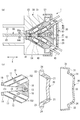
- the card edge connector 1 includes an inner housing (first housing) 10 and an outer housing (second housing) 50 for holding a circuit board 60. .
- the card edge connector 1 electrically connects the conductive pattern 65 formed on each of the front surface 61 and the back surface 63 of the circuit board 60 with another circuit board (not shown).
- the card edge connector 1 includes conductive patterns 65 arranged in two rows in the fitting direction x of the circuit board 60 and terminal fittings 40 arranged in two rows in the fitting direction held by the inner housing 10. There is a feature in electrically connecting.
- the front and rear thereof are defined according to the direction in which they are fitted to each other.
- the inner housing 10 is provided with a first movable housing 11 and a second movable housing 12 as shown in FIG. 1B, and holds the terminal fitting 40 respectively.
- the first movable housing 11 and the second movable housing 12 are swingably connected to each other within a predetermined range by a swing shaft 13.
- the first movable housing 11 and the second movable housing 12 sandwich the circuit board 60 from the side flat surface 63 side of the front surface 61.
- first movable housing 11 and the second movable housing 12 are different in the position where they are arranged in this way, they have the same configuration, and the same components are denoted by the same reference numerals, and in the following, the first movable housing 11 will be described. Further, both the first movable housing 11 and the second movable housing 12 are integrally formed by injection molding of an insulating resin.
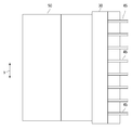
- the first movable housing 11 is provided with a cavity 15 that accommodates and holds a plurality of terminal fittings 40.
- the plurality of cavities 15 are arranged in the width direction y (FIG. 2) of the first movable housing 11 to form a single row of cavities.
- the cavity rows are arranged in two rows in the fitting direction x.
- the cavity 15 located on the front side may be referred to as a cavity 15 f
- the cavity 15 located on the rear side may be referred to as a cavity 15 r.
- the cavity 15 is generally referred to.
- the above-mentioned cavity 15 is formed in parallel to the guide surface 17 and includes a connection opening 151 opened in the holding surface 16 and a lead-out opening 152 opened in the rear end surface 18. Therefore, the cavity 15 is provided to be inclined with respect to the holding surface 16 and penetrates the first movable housing 11 in the front-rear direction.
- the contact 41 is exposed from the connection opening 151, and the electric wire 45 connected to the terminal fitting 40 is exposed to the outside from the extraction opening 152.
- a lance may be provided to hold the terminal fitting 40 to be accommodated so as to stay in a predetermined position and not to come out of the cavity 15.
- a rectangular parallelepiped fitting block 19 is formed at an intersection portion located on the front end side of the holding surface 16 and the guide surface 17.
- the fitting block 19 contacts the first guide surface 53 (the second movable housing 12 is the second guide surface 54) of the outer housing 50 in the process of fitting the inner housing 10 and the outer housing 50.
- the fitting block 19 is fitted in the fitting groove 55 of the outer housing 50 when the fitting is completed. The effects of the fitting block 19 in contact with the first guide surface 53 and the second guide surface 54 and the fitting thereof in the fitting groove 55 will be described later.
- the first movable housing 11 is provided with a support piece 14 projecting from the holding surface 16.
- the swing shaft 13 is provided so as to penetrate the support piece 14 of the first movable housing 11 and the support piece 14 of the second movable housing 12 which are disposed such that the holding surfaces 16 face each other.
- the first movable housing 11 and the second movable housing 12 are supported so as to be able to swing relative to each other.
- the waterproof seal 20 is provided inside the inner housing 10 in order to prevent water from entering from the side of the rear end surface 18 and between the inner housing 10 and the outer housing 50. Therefore, the waterproof seal 20 has a shape following the rear end surface 18 and is mounted without providing a gap with the rear end surface 18.
- the waterproof seal 20 has a surface area larger than the combined area of the rear end faces 18 of both the first movable housing 11 and the second movable housing 12, as shown in FIG. 1B, and is made of a flexible material such as rubber. It is a member which consists of In the waterproof seal 20, seal holes 21 penetrating the front and back are formed at positions corresponding to the plurality of cavities 15 of the first movable housing 11 and the second movable housing 12, respectively.
- the terminal fitting 40 When the terminal fitting 40 is inserted into the cavity 15, the terminal fitting 40 passes through the seal hole 21, and the electric wire 45 connected to the terminal fitting 40 penetrates the seal hole 21.
- the electric wire 45 passing through the seal hole 21 is in close contact with the periphery of the seal hole 21 to prevent the water having passed through the outlet opening 152 from entering the inside of the cavity 15.
- a seal block 23 is formed over the entire outer periphery.
- the seal block 23 is provided with three seal strips 24 protruding from the outer peripheral surface, and when the fitting of the inner housing 10 and the outer housing 50 is completed, the seal strips 24 are in close contact with the outer housing 50.
- the waterproof seal 20 prevents water from entering between the inner housing 10 and the outer housing 50.
- the cover 30 fixes the inner housing 10 and the waterproof seal 20 to the outer housing 50 by covering the waterproof seal 20 from the rear side.
- the cover 30 is provided with a first cover 31 corresponding to the first movable housing 11 and a second cover 32 corresponding to the second movable housing 12 as shown in FIG. They are pivotally connected to each other.
- the cover 30 When the cover 30 is assembled to the inner housing 10 via the waterproof seal 20, the cover 30 performs a rocking movement following the rocking movement of the first movable housing 11 and the second movable housing 12 of the inner housing 10.
- the angle between the holding surfaces 16 of the first movable housing 11 and the second movable housing 12 is smaller and closer to parallel is closed, and the larger angle between the two is open.
- wire holes 33 penetrating the front and back are formed at positions corresponding to the plurality of cavities 15 of the first movable housing 11 and the second movable housing 12, respectively. .
- the electric wire 45 passing through the seal hole 21 is drawn to the outside through the electric wire hole 33.
- the cover 30 is formed with the fitting sleeve 35 over the entire outer periphery. When the fitting is completed, the fitting sleeve 35 is fitted to the fitting sleeve 57 of the outer housing 50 from the outside, and the inner housing 10 and the outer housing 50 are prevented from coming off.
- the fitting sleeve 35 and the fitting sleeve 57 can be provided with locking projections (not shown) in order to ensure the integrity of the lock.
- the terminal fitting 40 is in the form of a socket as a whole, and as shown in FIG. 1B, the contact fitting 41 is integrally provided at the tip.
- the contactor 41 is formed thin so as to be elastically deformable, and a U-shaped folded back 42 is provided at the tip thereof.
- the tip end portion of the folded back 42 protrudes from the connection opening 151 by a very small amount.
- the terminal fitting 40 is manufactured using a metal material excellent in conductivity and elasticity, for example, a copper alloy.
- the outer housing 50 is fitted with the inner housing 10 while holding the circuit board 60, as shown in FIG. 1 (a).
- the outer housing 50 can also be used as part of the housing of the electronic device.
- the outer housing 50 comprises a receiving cavity 51 for receiving the inner housing 10.
- the receiving cavity 51 is opened at the front end of the outer housing 50 and is tapered so that the opening area of the longitudinal cross section is narrowed toward the rear end, and faces the first guide surface 53 and the second guide surface 54. It is.
- the first guide surface 53 and the second guide surface 54 intersect at a predetermined angle.
- the crossing angle substantially matches the angle formed by the first movable housing 11 of the inner housing 10 and the guide surfaces 17 of the second movable housing 12 which have been completely fitted.
- the first movable housing 11 and the second movable housing 12 can have the first guide surface 53 and the second guide surface 54, respectively. And slide towards the back of the receiving cavity 51.
- the first movable housing 11 and the second movable housing 12 are gradually closed as they progress toward the back of the receiving cavity 51.
- the terminal fitting 40 is held at a predetermined position of the cavity 15, and the waterproof seal 20 and the cover 30 are assembled.
- the inner housing 10 Prior to performing the fitting operation, the inner housing 10 is positioned in the receiving cavity 51 of the outer housing 50. This positioning is based on the premise that the circuit board 60 held by the outer housing 50 can be inserted between the first movable housing 11 and the second movable housing 12. Thereafter, the inner housing 10 is pushed toward the back of the receiving cavity 51.
- the first movable housing 11 and the second movable housing 12 are the most open.
- the front end side of the circuit board 60 is inserted between the first movable housing 11 and the second movable housing 12 as shown in FIG.
- the fitting block 19 of the first movable housing 11 is guided while sliding on the first guide surface 53
- the fitting block 19 of the second movable housing 12 is guided while sliding on the second guiding surface 54.
- the first movable housing 11 and the second movable housing 12 are closed more than originally. However, since the gap sufficiently exceeding the thickness of the circuit board 60 is left between the first movable housing 11 and the second movable housing 12, the terminal fitting 40 may contact the circuit board 60 from the beginning. Absent.
- the first movable housing 11 and the second movable housing 12 are closed, and the terminal fitting 40 approaches the circuit board 60.
- the seal strip 24 of the waterproof seal 20 abuts against the inner wall of the fitting sleeve 57 of the outer housing 50, and the fitting sleeve 35 of the inner housing 10 covers the rear end side of the fitting sleeve 57 .
- the fitting completion position shown in FIG. 1 is reached. Then, the terminal fitting 40 held by the first movable housing 11 contacts the conductive pattern 65 on the front surface 61 of the circuit board 60, and the terminal fitting 40 held by the second movable housing 12 is a circuit It contacts the conductive pattern 65 on the back surface 63 of the substrate 60.
- Each of the terminal fittings 40 starts contact with the conductive pattern 65 at a predetermined position slightly before reaching the fitting completion position, and continues to contact until the fitting completion position, thereby achieving the wiping effect.
- the contactors 41 of the terminal fittings 40 are elastically deformed by being pressed against the circuit board 60. The reaction force of the elastic deformation acts on the first movable housing 11 and the second movable housing 12 in a direction to open between the two.
- the fitting block 19 of the first movable housing 11 and the second movable housing 12 is inserted into the fitting groove 55. Since the force to open is applied to the first movable housing 11 and the second movable housing 12, each fitting block 19 is pressed against the upper wall 55 a and the lower wall 55 b facing the fitting groove 55. The pressing force contributes to preventing the inner housing 10 from coming out of the receiving cavity 51.
- the lock mechanism may be provided between the cover 30 and the outer housing 50 to prevent the inner housing 10 from coming out of the receiving cavity 51.
- the seal strip 24 of the waterproof seal 20 is in close contact with the inner wall of the fitting sleeve 57 of the outer housing 50, so that the entry of water into the receiving cavity 51 is prevented. Furthermore, when the fitting is completed, the fitting sleeve 35 of the cover 30 covers the periphery of the fitting sleeve 57.
- the card edge connector 1 has a plurality of terminal fittings 40 arranged in two rows on one side of the circuit board 60. Therefore, the card edge connector 1 can be multi-polarized as compared to the conventional card edge connector in which the terminal fittings are arranged in one row on one side. realizable.
- the reason why the terminal fittings 40 can be arranged in two rows in this way is that the terminal fittings 40 are inclined with respect to the circuit board 60. If the terminal fitting 40 is inclined to contact the circuit board 60, the terminal fitting 40 can be arranged in three or more rows.
- the terminal metal fitting 40 is retracted relative to the circuit board 60 until the fitting of the inner housing 10 and the outer housing 50 is completed, and it is slightly before reaching the fitting completion position.
- the terminal fitting 40 contacts the conductive pattern 65 of the circuit board 60. Therefore, since the inner housing 10 does not receive a reaction force caused by the contact of the terminal metal fitting 40 with the circuit board 60 in most of the area of the process of fitting, the card edge connector 1 can be multipolarized while being inner The force required to insert the housing 10 into the receiving cavity 51 can be reduced.
- the predetermined position at which the terminal fitting 40 starts to contact the conductive pattern 65 can be arbitrarily set in consideration of the reduction effect of the force for inserting the inner housing 10, the above-described wiping effect, and the like.
- the card edge connector 1 can prevent the terminal fitting 40 from hitting the tip of the circuit board 60 and damaging it, and the terminal fitting 40 slides on the front surface 61 and the back surface 63 of the circuit board 60
- the conductive pattern 65 can be prevented from peeling off.
- the above effect is realized by providing the condition that the inner housing 10 is configured to be able to open and close the first movable housing 11 and the second movable housing 12 and that both housings are closed as the fitting progresses. Ru.
- the configurations described in the above embodiments can be selected or changed to other configurations as appropriate without departing from the spirit of the present invention.
- the terminal metal fitting in contact with both the front surface and the back surface of the circuit board has been described.
- the present invention can also be applied to a card edge connector that contacts the terminal fitting.
- the waterproof seal 20 and the cover 30 are optional elements of the present invention, and may not be used depending on the application.
- the contact of the terminal metal fitting applied to this invention is equipped with U-shaped bending
Landscapes
- Coupling Device And Connection With Printed Circuit (AREA)
- Connector Housings Or Holding Contact Members (AREA)
Abstract
極数を増やすことのできるカードエッジコネクタを提供する。本発明のカードエッジコネクタは、一つの縁に沿って複数の導電パターン(65)が二列に形成された回路基板(60)を保持するアウターハウジング(50)と、アウターハウジング(50)と相互に嵌合され、回路基板(60)の導電パターン(65)の各々と電気的に接続される複数例に配列される端子金具(40)を保持するインナーハウジング(10)と、を備え、端子金具(40)は、回路基板(60)に対して同じ向きに傾斜して配列される。インナーハウジング(10)は、回路基板のおもて面(61)の側に配置される第1可動ハウジング(11)と、回路基板(60)のうら面の側に配置される第2可動ハウジング(12)と、からなり、第1可動ハウジング(11)と第2可動ハウジング(12)は、互いに揺動可能に連結される。
Description
本発明は、カードエッジコネクタに関し、特に多極化に対応できるカードエッジコネクタに関するものである。
従来から、プリント配線基板に代表される回路基板を、他の電気回路と接続するための電気コネクタとして、複数の導電パターンからなる端子を板状の周縁に沿って一列に備える回路基板と接続されるカードエッジ型のコネクタが知られている(例えば、特許文献1,2,3)。カードエッジコネクタは、端子金具が回路基板に対して平行に移動することで、周縁に設けられる回路基板側の端子と電気的に接続される。
カードエッジコネクタを含めて、電気コネクタは、端子の数をより多くする多極化の要請が大きい。カードエッジコネクタの多極化は、これまで、端子が一列に並ぶ方向の回路基板の寸法(幅)を大きくすることにより一列に並ぶ端子の数を増やすこと、及び、回路基板のおもて面及びうら面の両方に端子を設けること、で対応していた。
ところが、回路基板の幅を大きくすることは周囲の機器との関係で制約されるし、おもて面及びうら面を用いても未だ極数が不足することもある。
そこで本発明は、極数を増やすことのできるカードエッジコネクタを提供することを目的とする。
そこで本発明は、極数を増やすことのできるカードエッジコネクタを提供することを目的とする。
かかる目的のもと、本発明者らは、カードエッジコネクタの端子金具を回路基板に対して傾斜して接続させれば、端子金具及びカード側端子のそれぞれを二列あるいはそれ以上に配列できることを着想した。すなわち本発明のカードエッジコネクタは、一つの縁に沿って複数の導電パターンが複数列に形成された回路基板を保持する第2ハウジングと、第2ハウジングと相互に嵌合され、回路基板の導電パターンの各々と電気的に接続される複数例に配列される端子金具を保持する第1ハウジングと、を備える。そして、本発明のカードエッジコネクタは、端子金具が、回路基板に対して同じ向きに傾斜して配列されることを特徴とする。
本発明の好ましいカードエッジコネクタによれば、第1ハウジングが、回路基板の一方の面側に配置される第1可動ハウジングと、回路基板の他方の面側に配置される第2可動ハウジングと、を備え、第1可動ハウジングと第2可動ハウジングは、互いに揺動可能に連結される。また、第2ハウジングは、第1可動ハウジングと第2可動ハウジングを受容し、嵌合の完了位置に向けて、第1可動ハウジングと第2可動ハウジングを閉じる案内面を有する受容キャビティを備える。
この構成を備えるカードエッジコネクタは、第1ハウジングが、完了位置に向けて、第2ハウジングに挿入されることで、嵌合が完了する。一方で、端子金具は、嵌合の完了位置に到る手前の所定位置までは、回路基板から離れており、この所定位置から完了位置に到るまで、導電パターンと接触し続ける。したがって、本発明の好ましいカードエッジコネクタによれば、嵌合のほとんどの過程で、端子金具が回路基板に接触するのを避けることができるので、第1ハウジングを第2ハウジングに挿入するのに必要な力を抑えることができる。
この構成を備えるカードエッジコネクタは、第1ハウジングが、完了位置に向けて、第2ハウジングに挿入されることで、嵌合が完了する。一方で、端子金具は、嵌合の完了位置に到る手前の所定位置までは、回路基板から離れており、この所定位置から完了位置に到るまで、導電パターンと接触し続ける。したがって、本発明の好ましいカードエッジコネクタによれば、嵌合のほとんどの過程で、端子金具が回路基板に接触するのを避けることができるので、第1ハウジングを第2ハウジングに挿入するのに必要な力を抑えることができる。
本発明の好ましいカードエッジコネクタによれば、端子金具に接続される電線が引き出される後方側に防水シールを設けることができる。この防水シールは、第1可動ハウジングの後端、及び、第1ハウジングと第2ハウジングの間を封止する。
本発明の好ましいカードエッジコネクタによれば、端子金具は、導電パターンと接触する先端に、U字状に折り返される接触子を設けることができる。この接触子は、U字状に折り返されているので、適度な弾性を付与できるとともに、導電パターンに接触する部分が曲面になるので導電パターンに与える摩耗力を低く抑えることができる。
本発明によれば、カードエッジコネクタの端子金具を回路基板に対して傾斜させるので、端子金具を二列あるいはそれ以上に配列できる。したがって、本発明はカードエッジコネクタの多極化に寄与する。
以下、添付図面に示す実施の形態に基づいてこの発明を詳細に説明する。
本実施形態に係るカードエッジコネクタ1は、図1及び図2に示すように、インナーハウジング(第1ハウジング)10と、回路基板60を保持するアウターハウジング(第2ハウジング)50とを備えている。カードエッジコネクタ1は、回路基板60のおもて面61及びうら面63の各々に形成されている導電パターン65と、図示を省略する他の回路基板と、を電気的に接続する。このカードエッジコネクタ1は、回路基板60の嵌合方向xに二列に配列される導電パターン65と、インナーハウジング10に保持される嵌合方向に二列に配列される端子金具40と、を電気的に接続するところに特徴がある。以下、各構成要素を順に説明した後に、インナーハウジング10とアウターハウジング50の嵌合の手順について説明する。なお、インナーハウジング10とアウターハウジング50において、互いに嵌合される向きに従ってその前後を定義する。
本実施形態に係るカードエッジコネクタ1は、図1及び図2に示すように、インナーハウジング(第1ハウジング)10と、回路基板60を保持するアウターハウジング(第2ハウジング)50とを備えている。カードエッジコネクタ1は、回路基板60のおもて面61及びうら面63の各々に形成されている導電パターン65と、図示を省略する他の回路基板と、を電気的に接続する。このカードエッジコネクタ1は、回路基板60の嵌合方向xに二列に配列される導電パターン65と、インナーハウジング10に保持される嵌合方向に二列に配列される端子金具40と、を電気的に接続するところに特徴がある。以下、各構成要素を順に説明した後に、インナーハウジング10とアウターハウジング50の嵌合の手順について説明する。なお、インナーハウジング10とアウターハウジング50において、互いに嵌合される向きに従ってその前後を定義する。
[インナーハウジング10]
インナーハウジング10は、図1(b)に示すように、第1可動ハウジング11と第2可動ハウジング12を備えており、それぞれ、端子金具40を保持している。第1可動ハウジング11と第2可動ハウジング12は、揺動軸13により所定の範囲で互いに揺動可能に連結されている。第1可動ハウジング11と第2可動ハウジング12は、インナーハウジング10とアウターハウジング50が嵌合されると、回路基板60をおもて面61の側とうら面63の側から挟み込む。第1可動ハウジング11と第2可動ハウジング12は、このように配置される位置が相違するが、同じ構成を備えており、同じ構成部分については、同じ符号を付けて、以下では第1可動ハウジング11について説明する。また、第1可動ハウジング11と第2可動ハウジング12は、ともに、絶縁性の樹脂を射出成形することで、一体的に形成される。
インナーハウジング10は、図1(b)に示すように、第1可動ハウジング11と第2可動ハウジング12を備えており、それぞれ、端子金具40を保持している。第1可動ハウジング11と第2可動ハウジング12は、揺動軸13により所定の範囲で互いに揺動可能に連結されている。第1可動ハウジング11と第2可動ハウジング12は、インナーハウジング10とアウターハウジング50が嵌合されると、回路基板60をおもて面61の側とうら面63の側から挟み込む。第1可動ハウジング11と第2可動ハウジング12は、このように配置される位置が相違するが、同じ構成を備えており、同じ構成部分については、同じ符号を付けて、以下では第1可動ハウジング11について説明する。また、第1可動ハウジング11と第2可動ハウジング12は、ともに、絶縁性の樹脂を射出成形することで、一体的に形成される。
第1可動ハウジング11は、複数の端子金具40を収容し、かつ保持するキャビティ15を備えている。複数のキャビティ15は、第1可動ハウジング11の幅方向y(図2)に配列されることで、一列のキャビティ列をなしている。第1可動ハウジング11は、キャビティ列が、嵌合方向xに二列に並んでいる。二列のうちで、前側に位置するキャビティ15をキャビティ15fといい、後側に位置するキャビティ15をキャビティ15rということがある。ただし、両者を区別する必要がない場合には、キャビティ15と総称する。
第1可動ハウジング11は、アウターハウジング50と嵌合されると、回路基板60と対向する挟持面16と、挟持面16と所定の角度をなしてその一端と連なる案内面17と、挟持面16の他端と連なる後端面18と、を備えている。上述のキャビティ15は、案内面17と平行に形成されており、挟持面16に開口する接続開口151と、後端面18に開口する引出開口152と、を備えている。したがって、キャビティ15は、挟持面16に対して傾斜して設けられるとともに、第1可動ハウジング11を前後方向に貫通している。
キャビティ15に収容される端子金具40は、図1(a)に示すように、その接触子41が接続開口151から露出し、端子金具40に接続される電線45は、引出開口152から外部に向けて引き出される。
キャビティ15の内部には、収容される端子金具40が所定の位置に留まりキャビティ15から抜け出さないように保持するランスを設けることができる。
キャビティ15の内部には、収容される端子金具40が所定の位置に留まりキャビティ15から抜け出さないように保持するランスを設けることができる。
第1可動ハウジング11は、図11(b)に示すように、挟持面16と案内面17の前端側に位置する交差部分に、直方体状の嵌合ブロック19が形成されている。嵌合ブロック19は、インナーハウジング10とアウターハウジング50の嵌合の過程で、アウターハウジング50の第1案内面53(第2可動ハウジング12は、第2案内面54)に接触する。また、嵌合ブロック19は、嵌合が完了すると、アウターハウジング50の嵌合溝55に嵌合される。嵌合ブロック19が第1案内面53,第2案内面54に接触すること、また、嵌合溝55に嵌合されることによる効果については、後述する。
第1可動ハウジング11は、挟持面16から突出する支持片14を備えている。揺動軸13は、お互いの挟持面16が対向するように配置された第1可動ハウジング11の支持片14と第2可動ハウジング12の支持片14を貫通して設けられる。こうして、第1可動ハウジング11と第2可動ハウジング12を互いに揺動可能に支持される。
[防水シール20]
防水シール20は、インナーハウジング10の内部に後端面18の側から、及び、インナーハウジング10とアウターハウジング50の間から水が侵入するのを阻止するために設けられる。そのために、防水シール20は、後端面18に倣った形状を有しており、後端面18との間に隙間を設けることなく装着される。
防水シール20は、図1(b)に示すように、第1可動ハウジング11と第2可動ハウジング12の両者の後端面18を合せた面積よりも大きな表面積を有し、柔軟な素材、例えばゴムからなる部材である。
防水シール20は、第1可動ハウジング11と第2可動ハウジング12の複数のキャビティ15の各々に対応する位置に、表裏を貫通するシール孔21が形成されている。端子金具40はキャビティ15に挿入される際にシール孔21を通過し、端子金具40に接続される電線45がシール孔21を貫通する。シール孔21を貫通する電線45がシール孔21の周囲と密着されることで、引出開口152を通過した水がキャビティ15の内部に侵入するのを阻止する。
防水シール20は、シールブロック23が外周の全域に亘って形成されている。シールブロック23は、外周面から突き出す3本のシール条24を備えており、インナーハウジング10とアウターハウジング50の嵌合が完了すると、シール条24はアウターハウジング50に密着される。こうして、防水シール20は、インナーハウジング10とアウターハウジング50の間から水が侵入するのを阻止する。
[カバー30]
カバー30は、防水シール20を後側から覆って装着されることで、インナーハウジング10と防水シール20をアウターハウジング50に固定する。
カバー30は、図1(b)に示すように、第1可動ハウジング11に対応する第1カバー31と第2可動ハウジング12に対応する第2カバー32とを備えており、両者はヒンジ33により互いに揺動可能に連結されている。カバー30は、防水シール20を介してインナーハウジング10に組み付けられると、インナーハウジング10の第1可動ハウジング11と第2可動ハウジング12の揺動運動に追従して、揺動運動する。なお、本実施形態において、第1可動ハウジング11と第2可動ハウジング12の挟持面16同士のなす角度が小さくなり平行に近くなることを閉じると、いい、両者がなす角度が大きくなることを開く、という。
カバー30の第1カバー31と第2カバー32は、第1可動ハウジング11と第2可動ハウジング12の複数のキャビティ15の各々に対応する位置に、表裏を貫通する電線孔33が形成されている。シール孔21を貫通する電線45は電線孔33を介して外部に引き出される。
カバー30は、嵌合スリーブ35が外周の全域に亘って形成されている。嵌合スリーブ35は、嵌合が完了すると、アウターハウジング50の嵌合スリーブ57に外側から嵌合し、インナーハウジング10とアウターハウジング50が抜け止めされる。嵌合スリーブ35と嵌合スリーブ57は、ロックの完全性を担保するために、図示を省略するロック突起を設けることができる。
カバー30は、嵌合スリーブ35が外周の全域に亘って形成されている。嵌合スリーブ35は、嵌合が完了すると、アウターハウジング50の嵌合スリーブ57に外側から嵌合し、インナーハウジング10とアウターハウジング50が抜け止めされる。嵌合スリーブ35と嵌合スリーブ57は、ロックの完全性を担保するために、図示を省略するロック突起を設けることができる。
[端子金具40]
端子金具40は、全体としてソケットタイプの形態をなしており、図1(b)に示すように、先端に接触子41を一体的に備えている。接触子41は、弾性変形が可能なように薄肉に形成され、その先端にはU字状の折り返し42が設けられている。端子金具40は、インナーハウジング10のキャビティ15の所定位置に保持されると、折り返し42の先端部分が接続開口151から外部に微少量だけ突出している。
端子金具40は、導電性及び弾性に優れた金属材料、例えば銅合金を用いて作製される。
端子金具40は、全体としてソケットタイプの形態をなしており、図1(b)に示すように、先端に接触子41を一体的に備えている。接触子41は、弾性変形が可能なように薄肉に形成され、その先端にはU字状の折り返し42が設けられている。端子金具40は、インナーハウジング10のキャビティ15の所定位置に保持されると、折り返し42の先端部分が接続開口151から外部に微少量だけ突出している。
端子金具40は、導電性及び弾性に優れた金属材料、例えば銅合金を用いて作製される。
[アウターハウジング50]
アウターハウジング50は、図1(a)に示すように、回路基板60を保持しながら、インナーハウジング10と嵌合される。アウターハウジング50は、電子機器の筐体の一部が兼ねることもできる。
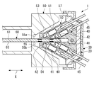
アウターハウジング50はインナーハウジング10を受容する受容キャビティ51を備えている。受容キャビティ51は、アウターハウジング50の前端に開口し、後端に向けて縦断面の開口面積が狭くなるようにテーパ状に形成されており、第1案内面53と第2案内面54に臨んでいる。
アウターハウジング50は、図1(a)に示すように、回路基板60を保持しながら、インナーハウジング10と嵌合される。アウターハウジング50は、電子機器の筐体の一部が兼ねることもできる。
アウターハウジング50はインナーハウジング10を受容する受容キャビティ51を備えている。受容キャビティ51は、アウターハウジング50の前端に開口し、後端に向けて縦断面の開口面積が狭くなるようにテーパ状に形成されており、第1案内面53と第2案内面54に臨んでいる。
第1案内面53と第2案内面54は、所定の角度をなして交差している。この交差角度は、嵌合が完了したインナーハウジング10の第1可動ハウジング11と第2可動ハウジング12の案内面17同士がなす角度とほぼ一致する。インナーハウジング10がアウターハウジング50の受容キャビティ51に挿入されると、第1可動ハウジング11と第2可動ハウジング12は、各々の嵌合ブロック19が第1案内面53と第2案内面54の各々を摺動しながら、受容キャビティ51の奥に向けて進む。第1可動ハウジング11と第2可動ハウジング12は、受容キャビティ51の奥に向けて進むにつれて、次第に閉じられる。
第1案内面53と第2案内面54の交差部分には、インナーハウジング10が受容キャビティ51の奥まで挿入されて嵌合が完了すると、第1可動ハウジング11の嵌合ブロック19と第2可動ハウジング12の嵌合ブロック19が一緒に嵌合される嵌合溝55が形成されている。
第1案内面53と第2案内面54の交差部分には、インナーハウジング10が受容キャビティ51の奥まで挿入されて嵌合が完了すると、第1可動ハウジング11の嵌合ブロック19と第2可動ハウジング12の嵌合ブロック19が一緒に嵌合される嵌合溝55が形成されている。
[嵌合過程の説明]
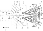
次に、インナーハウジング10とアウターハウジング50を相互に嵌合する過程を、図3~図5をも参照して説明する。なお、インナーハウジング10には、端子金具40がキャビティ15の所定位置に保持され、かつ、防水シール20及びカバー30が組み付けられているものとする。
嵌合作業を行うに先立って、インナーハウジング10をアウターハウジング50の受容キャビティ51に位置決めをする。この位置決めは、アウターハウジング50に保持される回路基板60が、第1可動ハウジング11と第2可動ハウジング12の間に挿入できる位置にあることが前提である。その後、インナーハウジング10を受容キャビティ51の奥に向けて押し込む。この嵌合初期の時点では、図3に示すように、第1可動ハウジング11と第2可動ハウジング12は最も開いている。
インナーハウジング10をさら受容キャビティ51の奥に向けて押し込むと、図4に示すように、回路基板60の前端側が第1可動ハウジング11と第2可動ハウジング12の間に挿入される。一方で、第1可動ハウジング11の嵌合ブロック19が第1案内面53に摺動しながら案内され、第2可動ハウジング12の嵌合ブロック19が第2案内面54に摺動しながら案内され、第1可動ハウジング11と第2可動ハウジング12は当初よりも閉じられる。しかし、第1可動ハウジング11と第2可動ハウジング12の間には、回路基板60の厚さを十分に超える間隙が残されているので、端子金具40は当初から回路基板60に接触することがない。
さらにインナーハウジング10を押し込むと、図5に示すように、第1可動ハウジング11と第2可動ハウジング12が閉じて、端子金具40は回路基板60に接近する。インナーハウジング10の後端側では、防水シール20のシール条24がアウターハウジング50の嵌合スリーブ57の内壁に突き当たるとともに、インナーハウジング10の嵌合スリーブ35が嵌合スリーブ57の後端側を覆う。
さらに、インナーハウジング10を受容キャビティ51の奥まで押し込むと、図1に示す嵌合の完了位置に到る。そうすると、第1可動ハウジング11に保持されている端子金具40は、回路基板60のおもて面61の導電パターン65に接触し、第2可動ハウジング12に保持されている端子金具40は、回路基板60のうら面63の導電パターン65に接触する。各端子金具40は、嵌合完了の位置に到る少し手前の所定位置において導電パターン65と接触を開始し、そのまま嵌合完了の位置まで接触し続けることで、ワイピングの効果を奏する。また、各端子金具40の接触子41は、回路基板60に押し付けられることで、弾性変形する。この弾性変形の反力により、第1可動ハウジング11と第2可動ハウジング12には、両者の間に開こうとする向きの力が作用する。
また、嵌合完了に到ると、第1可動ハウジング11及び第2可動ハウジング12の嵌合ブロック19は、嵌合溝55の中に挿入される。第1可動ハウジング11と第2可動ハウジング12には開こうとする力が作用しているので、各々の嵌合ブロック19は嵌合溝55に臨む上壁55aと下壁55bに押し付けられる。この押し付け力は、インナーハウジング10が受容キャビティ51から抜け出るのを防止するのに寄与する。ただし、本実施形態は、カバー30とアウターハウジング50の間にロック機構を設けることで、インナーハウジング10の受容キャビティ51からの抜け止めを図ることもできる。
また、嵌合完了に到ると、防水シール20のシール条24がアウターハウジング50の嵌合スリーブ57の内壁に密着されるので、受容キャビティ51の中へ水が侵入するのが妨げられる。さらに、嵌合完了に到ると、カバー30の嵌合スリーブ35が嵌合スリーブ57の周囲を覆う。
[実施形態の効果]
次に、カードエッジコネクタ1による効果を説明する。
カードエッジコネクタ1は、回路基板60の一方の面について、複数の端子金具40を二列に配列するので、一方の面に端子金具を一列だけ配列する従来のカードエッジコネクタに比べて、多極化を実現できる。このように端子金具40を二列に配列できるのは、端子金具40を回路基板60に対して傾斜させているからである。回路基板60に対して端子金具40を傾斜させて接触させる手法を用いれば、端子金具40を三列以上に配列することもできる。
次に、カードエッジコネクタ1による効果を説明する。
カードエッジコネクタ1は、回路基板60の一方の面について、複数の端子金具40を二列に配列するので、一方の面に端子金具を一列だけ配列する従来のカードエッジコネクタに比べて、多極化を実現できる。このように端子金具40を二列に配列できるのは、端子金具40を回路基板60に対して傾斜させているからである。回路基板60に対して端子金具40を傾斜させて接触させる手法を用いれば、端子金具40を三列以上に配列することもできる。
次に、カードエッジコネクタ1は、インナーハウジング10とアウターハウジング50の嵌合が完了する前までは端子金具40が回路基板60に対して退避しており、嵌合完了位置に到る少し手前の所定位置で始めて端子金具40は回路基板60の導電パターン65に接触する。
したがって、インナーハウジング10は、嵌合の過程のほとんどの領域において、端子金具40が回路基板60に接触することによる反力を受けないので、カードエッジコネクタ1は、多極化が可能でありながら、インナーハウジング10を受容キャビティ51に挿入するのに必要な力を低減できる。なお、端子金具40が導電パターン65に接触し始める所定位置は、インナーハウジング10を挿入する力の低減効果、前述したワイピング効果などを考慮して任意に設定することができる。
また、カードエッジコネクタ1は、端子金具40が回路基板60の先端に突き当たって損傷するのを避けることができるとともに、端子金具40が回路基板60のおもて面61およびうら面63を摺動して導電パターン65が剥離するのを防ぐことができる。
以上の効果は、インナーハウジング10が第1可動ハウジング11と第2可動ハウジング12が開閉可能に構成されており、かつ、嵌合が進むのにつれて両ハウジングが閉じる、という要件を備えることにより実現される。
以上、本発明の好適な実施形態を説明したが、本発明の主旨を逸脱しない限り、上記実施の形態で挙げた構成を取捨選択したり、他の構成に適宜変更することが可能である。
例えば、本実施形態のカードエッジコネクタは、回路基板のおもて面及びうら面の両方に端子金具が接触する例を説明したが、本発明は、いずれか一方の面だけに複数列に配列された端子金具を接触するカードエッジコネクタに適用することもできる。
また、防水シール20及びカバー30は、本発明の任意の要素であり、適用対象によっては用いられないこともある。
また、本発明に適用される端子金具の接触子は、U字状の折り返しを備えることが好ましいが、適度な弾性を備えている限り、その形態は問われない。
例えば、本実施形態のカードエッジコネクタは、回路基板のおもて面及びうら面の両方に端子金具が接触する例を説明したが、本発明は、いずれか一方の面だけに複数列に配列された端子金具を接触するカードエッジコネクタに適用することもできる。
また、防水シール20及びカバー30は、本発明の任意の要素であり、適用対象によっては用いられないこともある。
また、本発明に適用される端子金具の接触子は、U字状の折り返しを備えることが好ましいが、適度な弾性を備えている限り、その形態は問われない。
1 カードエッジコネクタ
10 インナーハウジング
11 第1可動ハウジング
12 第2可動ハウジング
13 揺動軸
15f,15r(15) キャビティ
16 挟持面
17 案内面
18 後端面
19 嵌合ブロック
20 防水シール
30 カバー
40 端子金具
41 接触子
42 折り返し
50 アウターハウジング
51 受容キャビティ
53 第1案内面
54 第2案内面
55 嵌合溝
60 回路基板
61 おもて面
63 うら面
65 導電パターン
10 インナーハウジング
11 第1可動ハウジング
12 第2可動ハウジング
13 揺動軸
15f,15r(15) キャビティ
16 挟持面
17 案内面
18 後端面
19 嵌合ブロック
20 防水シール
30 カバー
40 端子金具
41 接触子
42 折り返し
50 アウターハウジング
51 受容キャビティ
53 第1案内面
54 第2案内面
55 嵌合溝
60 回路基板
61 おもて面
63 うら面
65 導電パターン
Claims (5)
- 一つの縁に沿って複数の導電パターンが複数列に形成された回路基板を保持する第2ハウジングと、
前記第2ハウジングと相互に嵌合され、前記回路基板の前記導電パターンの各々と電気的に接続される複数例に配列される端子金具を保持する第1ハウジングと、を備え、
前記端子金具は、前記回路基板に対して同じ向きに傾斜して配列される、ことを特徴とするカードエッジコネクタ。 - 前記第1ハウジングは、
前記回路基板の一方の面側に配置される第1可動ハウジングと、
前記回路基板の他方の面側に配置される第2可動ハウジングと、を備え、
前記第1可動ハウジングと前記第2可動ハウジングは、互いに揺動可能に連結され、
前記第2ハウジングは、
前記第1可動ハウジングと前記第2可動ハウジングを受容し、嵌合の完了位置に向けて、前記第1可動ハウジングと前記第2可動ハウジングを閉じる案内面を有する受容キャビティを備える、請求項1に記載のカードエッジコネクタ。 - 前記端子金具は、
前記完了位置に到る手前の所定位置までは、前記回路基板から離れており、
前記所定位置から前記完了位置に到るまで、前記導電パターンと接触し続ける、請求項2に記載のカードエッジコネクタ。 - 前記端子金具に接続される電線が引き出される後方側に設けられ、
前記第1ハウジングの後端、及び、前記第1ハウジングと前記第2ハウジングの間を封止する防水シールを備える、請求項1~請求項3のいずれか一項に記載のカードエッジコネクタ。 - 前記端子金具は、
前記導電パターンと接触する先端に、U字状に折り返される接触子が設けられる、 請求項1~請求項4のいずれか一項に記載のカードエッジコネクタ。
Priority Applications (1)
| Application Number | Priority Date | Filing Date | Title |
|---|---|---|---|
| CN201480061294.7A CN105684224B (zh) | 2013-11-08 | 2014-11-04 | 卡片边缘连接器 |
Applications Claiming Priority (2)
| Application Number | Priority Date | Filing Date | Title |
|---|---|---|---|
| JP2013231792A JP6283202B2 (ja) | 2013-11-08 | 2013-11-08 | カードエッジコネクタ |
| JP2013-231792 | 2013-11-08 |
Publications (1)
| Publication Number | Publication Date |
|---|---|
| WO2015068689A1 true WO2015068689A1 (ja) | 2015-05-14 |
Family
ID=53041466
Family Applications (1)
| Application Number | Title | Priority Date | Filing Date |
|---|---|---|---|
| PCT/JP2014/079225 WO2015068689A1 (ja) | 2013-11-08 | 2014-11-04 | カードエッジコネクタ |
Country Status (3)
| Country | Link |
|---|---|
| JP (1) | JP6283202B2 (ja) |
| CN (1) | CN105684224B (ja) |
| WO (1) | WO2015068689A1 (ja) |
Families Citing this family (3)
| Publication number | Priority date | Publication date | Assignee | Title |
|---|---|---|---|---|
| JP7432990B2 (ja) * | 2018-11-13 | 2024-02-19 | タイコエレクトロニクスジャパン合同会社 | 電気機器 |
| US11916324B2 (en) | 2021-07-08 | 2024-02-27 | Cisco Technology, Inc. | Connecting multi-conductor cables with surface contacts |
| WO2023283534A1 (en) * | 2021-07-08 | 2023-01-12 | Cisco Technology, Inc. | Connecting multi-conductor cables with surface contacts |
Citations (2)
| Publication number | Priority date | Publication date | Assignee | Title |
|---|---|---|---|---|
| JPH0837065A (ja) * | 1993-10-28 | 1996-02-06 | Sumitomo Wiring Syst Ltd | カードエッジコネクタ |
| JP2011086457A (ja) * | 2009-10-14 | 2011-04-28 | Yazaki Corp | 防水コネクタ |
Family Cites Families (3)
| Publication number | Priority date | Publication date | Assignee | Title |
|---|---|---|---|---|
| EP0273589B1 (en) * | 1986-12-22 | 1993-09-01 | The Whitaker Corporation | High density coax connector |
| DE19511508C2 (de) * | 1995-03-29 | 1998-07-09 | Siemens Ag | Elektrischer Leiterplattenverbinder |
| JP2012212613A (ja) * | 2011-03-31 | 2012-11-01 | Fujitsu Component Ltd | フローティング機能付きカードエッジコネクタ |
-
2013
- 2013-11-08 JP JP2013231792A patent/JP6283202B2/ja active Active
-
2014
- 2014-11-04 WO PCT/JP2014/079225 patent/WO2015068689A1/ja active Application Filing
- 2014-11-04 CN CN201480061294.7A patent/CN105684224B/zh active Active
Patent Citations (2)
| Publication number | Priority date | Publication date | Assignee | Title |
|---|---|---|---|---|
| JPH0837065A (ja) * | 1993-10-28 | 1996-02-06 | Sumitomo Wiring Syst Ltd | カードエッジコネクタ |
| JP2011086457A (ja) * | 2009-10-14 | 2011-04-28 | Yazaki Corp | 防水コネクタ |
Also Published As
| Publication number | Publication date |
|---|---|
| CN105684224B (zh) | 2018-09-28 |
| JP6283202B2 (ja) | 2018-02-21 |
| CN105684224A (zh) | 2016-06-15 |
| JP2015092440A (ja) | 2015-05-14 |
Similar Documents
| Publication | Publication Date | Title |
|---|---|---|
| JP4945596B2 (ja) | スイッチ付き同軸コネクタ及びその組み立て方法 | |
| JP4519172B2 (ja) | コネクタ | |
| JP5193888B2 (ja) | コネクタ | |
| WO2004095642A3 (en) | Electrical connector having connector position assurance member | |
| JP2004165046A (ja) | 平型導体の接続のための電気コネクタ | |
| TWI623161B (zh) | 電連接器 | |
| JP3025948B2 (ja) | 平型柔軟ケーブル用コネクタ | |
| US20180351271A1 (en) | Plug-in contact | |
| JP2006228446A (ja) | コネクタ | |
| WO2015068692A1 (ja) | 端子金具、及び、それを備える電気コネクタ | |
| CN201438578U (zh) | Usb电连接器 | |
| JP5472608B2 (ja) | 基板コネクタ装置 | |
| WO2015068689A1 (ja) | カードエッジコネクタ | |
| TW200638618A (en) | Flat circuit connector | |
| CN104577449A (zh) | 带退卡机构的卡座 | |
| JP2002246088A (ja) | 可撓性平型ケーブル用防水コネクタ | |
| JP2013168339A (ja) | 同軸低背コネクタ | |
| JP3555482B2 (ja) | 小型コネクタ | |
| ATE425566T1 (de) | Abgedichteter verbinder mit sequenzieller schliessung | |
| JP5618748B2 (ja) | コネクタ | |
| US7559792B2 (en) | Connector with easily replacement of a slider | |
| JP4228978B2 (ja) | コネクタ | |
| CN108199200B (zh) | 连接器 | |
| JP3650842B2 (ja) | 電線コネクタ | |
| TWM413995U (en) | Water-proof connector |
Legal Events
| Date | Code | Title | Description |
|---|---|---|---|
| 121 | Ep: the epo has been informed by wipo that ep was designated in this application |
Ref document number: 14859913 Country of ref document: EP Kind code of ref document: A1 |
|
| NENP | Non-entry into the national phase |
Ref country code: DE |
|
| 122 | Ep: pct application non-entry in european phase |
Ref document number: 14859913 Country of ref document: EP Kind code of ref document: A1 |