WO2015068433A1 - 圧着装置、及び、表示装置の製造方法 - Google Patents
圧着装置、及び、表示装置の製造方法 Download PDFInfo
- Publication number
- WO2015068433A1 WO2015068433A1 PCT/JP2014/069434 JP2014069434W WO2015068433A1 WO 2015068433 A1 WO2015068433 A1 WO 2015068433A1 JP 2014069434 W JP2014069434 W JP 2014069434W WO 2015068433 A1 WO2015068433 A1 WO 2015068433A1
- Authority
- WO
- WIPO (PCT)
- Prior art keywords
- crimping
- terminal
- anisotropic conductive
- ultraviolet rays
- portions
- Prior art date
- Legal status (The legal status is an assumption and is not a legal conclusion. Google has not performed a legal analysis and makes no representation as to the accuracy of the status listed.)
- Ceased
Links
Images




Classifications
-
- H—ELECTRICITY
- H10—SEMICONDUCTOR DEVICES; ELECTRIC SOLID-STATE DEVICES NOT OTHERWISE PROVIDED FOR
- H10W—GENERIC PACKAGES, INTERCONNECTIONS, CONNECTORS OR OTHER CONSTRUCTIONAL DETAILS OF DEVICES COVERED BY CLASS H10
- H10W72/00—Interconnections or connectors in packages
- H10W72/071—Connecting or disconnecting
- H10W72/0711—Apparatus therefor
-
- H—ELECTRICITY
- H10—SEMICONDUCTOR DEVICES; ELECTRIC SOLID-STATE DEVICES NOT OTHERWISE PROVIDED FOR
- H10W—GENERIC PACKAGES, INTERCONNECTIONS, CONNECTORS OR OTHER CONSTRUCTIONAL DETAILS OF DEVICES COVERED BY CLASS H10
- H10W72/00—Interconnections or connectors in packages
- H10W72/071—Connecting or disconnecting
- H10W72/0711—Apparatus therefor
- H10W72/07141—Means for applying energy, e.g. ovens or lasers
-
- H—ELECTRICITY
- H10—SEMICONDUCTOR DEVICES; ELECTRIC SOLID-STATE DEVICES NOT OTHERWISE PROVIDED FOR
- H10W—GENERIC PACKAGES, INTERCONNECTIONS, CONNECTORS OR OTHER CONSTRUCTIONAL DETAILS OF DEVICES COVERED BY CLASS H10
- H10W72/00—Interconnections or connectors in packages
- H10W72/071—Connecting or disconnecting
- H10W72/0711—Apparatus therefor
- H10W72/07173—Means for moving chips, wafers or other parts, e.g. conveyor belts
-
- H—ELECTRICITY
- H10—SEMICONDUCTOR DEVICES; ELECTRIC SOLID-STATE DEVICES NOT OTHERWISE PROVIDED FOR
- H10W—GENERIC PACKAGES, INTERCONNECTIONS, CONNECTORS OR OTHER CONSTRUCTIONAL DETAILS OF DEVICES COVERED BY CLASS H10
- H10W72/00—Interconnections or connectors in packages
- H10W72/071—Connecting or disconnecting
- H10W72/073—Connecting or disconnecting of die-attach connectors
- H10W72/07331—Connecting techniques
- H10W72/07337—Connecting techniques using a polymer adhesive, e.g. an adhesive based on silicone or epoxy
- H10W72/07338—Connecting techniques using a polymer adhesive, e.g. an adhesive based on silicone or epoxy hardening the adhesive by curing, e.g. thermosetting
-
- H—ELECTRICITY
- H10—SEMICONDUCTOR DEVICES; ELECTRIC SOLID-STATE DEVICES NOT OTHERWISE PROVIDED FOR
- H10W—GENERIC PACKAGES, INTERCONNECTIONS, CONNECTORS OR OTHER CONSTRUCTIONAL DETAILS OF DEVICES COVERED BY CLASS H10
- H10W72/00—Interconnections or connectors in packages
- H10W72/071—Connecting or disconnecting
- H10W72/074—Connecting or disconnecting of anisotropic conductive adhesives
-
- H—ELECTRICITY
- H10—SEMICONDUCTOR DEVICES; ELECTRIC SOLID-STATE DEVICES NOT OTHERWISE PROVIDED FOR
- H10W—GENERIC PACKAGES, INTERCONNECTIONS, CONNECTORS OR OTHER CONSTRUCTIONAL DETAILS OF DEVICES COVERED BY CLASS H10
- H10W72/00—Interconnections or connectors in packages
- H10W72/30—Die-attach connectors
- H10W72/321—Structures or relative sizes of die-attach connectors
- H10W72/325—Die-attach connectors having a filler embedded in a matrix
-
- H—ELECTRICITY
- H10—SEMICONDUCTOR DEVICES; ELECTRIC SOLID-STATE DEVICES NOT OTHERWISE PROVIDED FOR
- H10W—GENERIC PACKAGES, INTERCONNECTIONS, CONNECTORS OR OTHER CONSTRUCTIONAL DETAILS OF DEVICES COVERED BY CLASS H10
- H10W72/00—Interconnections or connectors in packages
- H10W72/30—Die-attach connectors
- H10W72/351—Materials of die-attach connectors
-
- H—ELECTRICITY
- H10—SEMICONDUCTOR DEVICES; ELECTRIC SOLID-STATE DEVICES NOT OTHERWISE PROVIDED FOR
- H10W—GENERIC PACKAGES, INTERCONNECTIONS, CONNECTORS OR OTHER CONSTRUCTIONAL DETAILS OF DEVICES COVERED BY CLASS H10
- H10W90/00—Package configurations
- H10W90/701—Package configurations characterised by the relative positions of pads or connectors relative to package parts
- H10W90/731—Package configurations characterised by the relative positions of pads or connectors relative to package parts of die-attach connectors
- H10W90/734—Package configurations characterised by the relative positions of pads or connectors relative to package parts of die-attach connectors between a chip and a stacked insulating package substrate, interposer or RDL
Definitions
- the present invention relates to a crimping device and a method for manufacturing a display device. More specifically, a crimping device suitably used for crimping a circuit member and a terminal portion (hereinafter also simply referred to as a terminal portion) provided on the display panel, and a circuit member and a terminal using the crimping device.
- the present invention relates to a method for manufacturing a display device that performs pressure bonding with a portion.
- a circuit member is usually pressure-bonded to a terminal portion provided at an end portion of the display panel via an anisotropic conductive film (ACF) or the like.
- ACF anisotropic conductive film
- a COG (Chip on Glass) process and an FOG (Film on Glass) process are known.
- an integrated circuit (IC: Integrated Circuit) and a terminal part are pressure-bonded via an ACF.
- the IC input / output bumps and the terminal portions are electrically connected via conductive particles made of gold or the like that are uniformly present in the ACF.
- a flexible printed circuit (FPC) and a terminal part are pressure-bonded via an ACF.
- a pressure connection device comprising a backup tool divided into a plurality of backup sections, a pressure tool, and a support means for displacing each backup section in accordance with the difference in pressure applied by the pressure tools applied to the plurality of backup sections.
- the semiconductor element is fixed on the light-transmitting substrate by irradiating light onto the reflective table surface from the light irradiation device through the light-transmitting substrate and exposing the reflected light to a photo-curing resin to solidify.
- a method for mounting a semiconductor element is known (for example, see Patent Document 3).
- a manufacturing method of a liquid crystal display device in which an electrode portion of a semiconductor element and a connection electrode of a liquid crystal display element are connected via an ACF that is cured by heat and ultraviolet rays (for example, see Patent Document 4).
- pressure bonding between the circuit member and the terminal portion as described above is mainly performed at a low temperature. This can reduce the heat load on the display surface of the display panel and the polarizing plate attached to the display panel, or can be a member having a different linear expansion coefficient (for example, a combination of an IC and a display panel, or an FPC). This is because it is desired to reduce the warpage during the thermocompression bonding of the display panel and the display panel.
- ACF cured with ultraviolet rays and ACF cured with heat and ultraviolet rays is underway.
- the crimping is performed individually or in a plurality. This is because the distance between ICs is narrowed due to the narrower frame and higher definition of the display panel, and further, high-pressure crimping is required from the viewpoint of sufficiently improving connection reliability. This is because it is difficult to adjust the distance to the distance between the ICs. In order to cope with such a problem, a method described below has been conventionally used.
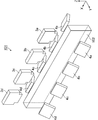
- FIG. 7 is a perspective view showing a conventional crimping apparatus.
- the crimping apparatus 101 includes a support unit 102, a plurality of movable crimping units 3 a, 3 b, 3 c, and 3 d that face the support unit 102, and a plurality of light source units arranged in the vicinity of the support unit 102. 4a, 4b, 4c, 4d.
- the support portion 102 has a shape extending along the X direction, and supports a plurality of terminal portions on which a plurality of circuit members are placed.
- Each movable crimping portion is disposed along the X direction and can be driven in the Z direction, and can press a plurality of circuit members and a plurality of terminal portions disposed on the support portion 102.
- Each light source part is arranged along the X direction so as to correspond to each movable pressure-bonding part. From the support part 102 side, a plurality of circuit members arranged on the support part 102 and a joint part of a plurality of terminal parts Irradiate with UV rays.
- compression-bonding part usually incorporate the heat source (not shown) for using for crimping
- FIG. 8 is an explanatory view showing a state in which an IC and a terminal portion are crimped using a conventional crimping apparatus.
- a plurality of terminal portions 7a, 7b, 7c, 7d provided on the liquid crystal display panel 6 are respectively passed through a plurality of ACFs 8a, 8b, 8c, 8d that are cured by heat and ultraviolet rays.
- a plurality of ICs 9a, 9b, 9c, 9d are placed in advance. Further, the liquid crystal display panel 6 can be moved in the X, Y, and Z directions by a drive source (not shown).
- the COG process using the conventional crimping apparatus 101 is sequentially performed in the following flows (1) to (8), for example.
- Such a method is one of the coping methods when the distance between the movable crimping parts is longer than the distance between the ICs and adjacent ICs cannot be crimped simultaneously.
- (1) The liquid crystal display panel 6 is placed on the support portion 102, and the IC 9a and the movable crimping portion 3a are aligned.
- the ACF 8a While pressing the IC 9a and the terminal portion 7a with the movable crimping portion 3a, the ACF 8a is irradiated with ultraviolet rays from the light source portion 4a to cure the ACF 8a.
- the liquid crystal display panel 6 is moved to align the IC 9b and the movable crimping part 3b. (4) While pressing the IC 9b and the terminal portion 7b with the movable crimping portion 3b, the ACF 8b is irradiated with ultraviolet rays from the light source portion 4b to cure the ACF 8b. (5) The liquid crystal display panel 6 is moved to align the IC 9c and the movable crimping portion 3c. (6) While pressing the IC 9c and the terminal portion 7c with the movable crimp portion 3c, the ACF 8c is irradiated with ultraviolet rays from the light source portion 4c to cure the ACF 8c.
- the liquid crystal display panel 6 is moved to align the IC 9d and the movable crimping part 3d.
- the ACF 8d While pressing the IC 9d and the terminal portion 7d with the movable crimping portion 3d, the ACF 8d is irradiated with ultraviolet rays from the light source portion 4d to cure the ACF 8d.
- the irradiation of ultraviolet rays in the above (2), (4), (6), (8) is simultaneous with or delayed from the start of pressing of each movable pressure-bonding part (for example, 1 to 2 seconds from the start of pressing) After) done.
- each ACF is hardened by irradiating with an ultraviolet-ray, heating with the heat source (not shown) incorporated in the support part 102 and each movable crimping
- the flow of (1) to (8) is a method of sequentially crimping individual ICs, but there is also a method of crimping for each of a plurality of ICs.
- the following (A) to (D) A method that is sequentially performed in the flow can be mentioned. This is a method of simultaneously pressing two ICs arranged every other.
- (A) The liquid crystal display panel 6 is placed on the support portion 102, and the alignment of the IC 9a and the movable crimp portion 3a and the alignment of the IC 9c and the movable crimp portion 3c are simultaneously performed.
- the ACF 8b While pressing the IC 9b and the terminal part 7b with the movable crimping part 3b, the ACF 8b is irradiated with ultraviolet rays from the light source part 4b to cure the ACF 8b, and while pressing the IC 9d and the terminal part 7d with the movable crimping part 3d.
- the ACF 8d is irradiated with ultraviolet rays from the light source unit 4d to cure the ACF 8d at the same time.
- the conditions (B) and (D) for example, the same conditions as (2), (4), (6), and (8) can be used.
- the conventional crimping apparatus 101 when the target ACF (for example, ACF 8 a) is irradiated with ultraviolet rays, the ultraviolet rays propagate through the support portion 102, so that the uncured ACF (for example, ACF 8 b) that is not the target.
- the curing reaction also proceeds, and as a result, connection failure between the IC (for example, IC 9b) and the terminal portion (for example, terminal portion 7b) may occur, and the connection reliability may be lowered.
- the conventional crimping apparatus 101 has room for improvement in terms of preventing poor connection between the circuit member and the terminal portion.
- Patent Document 1 provides a method for manufacturing an electro-optical device that can electrically connect terminals after positioning a terminal of a transparent substrate and a terminal of an electronic component without degrading the electro-optical material. Disclosure. However, the invention described in Patent Document 1 is intended to prevent light irradiation to an electro-optic material (for example, liquid crystal), and there is room for improvement to solve the above-described problem.
- an electro-optic material for example, liquid crystal
- Patent Document 2 discloses that when two electronic components are connected by pressurization, an electronic component pressurizing and connecting apparatus is provided which can pressurize and connect these electronic components uniformly.
- the invention described in Patent Document 2 does not suggest the use of ACF that is cured by ultraviolet rays or ACF that is cured by heat and ultraviolet rays, and there is room for contrivance to solve the above problems. .
- Patent Document 3 discloses that a semiconductor element mounting method for obtaining a highly reliable semiconductor element mounting product is provided.
- the invention described in Patent Document 3 does not suggest the above problem, and there is room for improvement to solve the above problem.
- Patent Document 4 discloses that a method for manufacturing a liquid crystal display device that easily realizes stable and low resistance connection is disclosed regarding connection between an electrode portion of a semiconductor element and a connection electrode of a liquid crystal display element.
- the invention described in Patent Document 4 does not suggest the above problem, and there is room for improvement to solve the above problem.
- This invention is made
- compression-bonding apparatus which can prevent the connection failure between a circuit member and a terminal part, and the crimping
- the inventors of the present invention have made various studies on a crimping apparatus that can prevent a connection failure between a circuit member and a terminal part.
- the support part is divided into a plurality of parts, and a plurality of parts are provided in the gaps of the divided support parts. Focusing on the arrangement of the ultraviolet light shielding member. With such a configuration, when irradiating the target ACF with ultraviolet rays, the ultraviolet rays to the uncured ACF that is not the target can be shielded. It was found that it can be prevented.
- the inventors have conceived that the above problems can be solved brilliantly and have reached the present invention.
- one embodiment of the present invention is a crimping apparatus that crimps a plurality of circuit members and a plurality of terminal portions provided on a display panel, wherein the plurality of terminal portions on which the plurality of circuit members are placed A plurality of supporting portions to be supported; a plurality of movable crimping portions capable of pressing the plurality of circuit members and the plurality of terminal portions disposed on the plurality of supporting portions; and the plurality of supporting portions from the plurality of supporting portion sides.
- a plurality of light sources that irradiate ultraviolet rays toward the joints of the plurality of circuit members and the plurality of terminal portions disposed on the support portion; and a plurality of ultraviolet light shields disposed in the gaps between the plurality of support portions.
- compression-bonding apparatus which has a member may be sufficient.
- Another embodiment of the present invention may be a method for manufacturing a display device including a step of crimping the plurality of circuit members and the plurality of terminal portions using the crimping device.
- a crimping device that can prevent a connection failure between a circuit member and a terminal portion, and a method for manufacturing a display device that crimps a circuit member and a terminal portion using the crimping device. Can be provided.
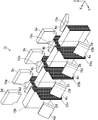
- FIG. 1 is a perspective view showing a crimping apparatus according to Embodiment 1.
- FIG. It is a perspective view which shows the conventional crimping
- the present invention relates to a crimping apparatus that crimps a plurality of circuit members and a plurality of terminal portions provided on the display panel, and a combination of the plurality of circuit members and the display panel is not particularly limited.
- a COG process in which an IC is used as a circuit member and a liquid crystal display panel is used as a display panel will be described.
- the liquid crystal display panel a liquid crystal display panel that requires a large number of circuit members, such as in-vehicle, tablet, and industrial equipment (IA) applications, is preferably used.
- Embodiment 1 relates to a configuration in which a support portion is divided into a plurality of parts and a plurality of ultraviolet light shielding members are arranged so as to fill gaps between the plurality of support portions with respect to a conventional crimping apparatus. Moreover, it is related with the COG process including the process of crimping
- FIG. 1 is a perspective view showing the crimping apparatus according to the first embodiment.
- the crimping apparatus 1a includes a plurality of support portions 2a, 2b, 2c, and 2d, a plurality of movable pressure-bonding portions 3a, 3b, 3c, and 3d that face each support portion, and the vicinity of each support portion.
- a plurality of light source portions 4a, 4b, 4c, and 4d arranged in the above, and a plurality of ultraviolet light shielding members 5a, 5b, and 5c arranged so as to fill the gaps between the support portions.
- the support portions 2a, 2b, 2c, and 2d are arranged along the X direction, and support a plurality of terminal portions on which a plurality of ICs are placed. From the viewpoint of performing support with high accuracy, the length of each support portion in the X direction is preferably equal to or greater than the length of the IC in the X direction.
- the movable crimping portions 3a, 3b, 3c, and 3d are arranged along the X direction and can be driven in the Z direction, and a plurality of circuit members and a plurality of circuit members arranged on the support portions 2a, 2b, 2c, and 2d. Can be pressed.
- the length of each movable crimping portion in the Y direction is, for example, about 3 to 5 mm. Further, the length in the X direction of each movable crimping portion depends on the size of the IC to be crimped.
- each movable crimping part when the length of the IC in the X direction is 8 to 30 mm, the length in the X direction of each movable crimping portion is about 35 mm so that an IC with a maximum length of 30 mm can be crimped. Yes.
- each movable crimping part usually incorporates a heat source (not shown) for use in crimping.
- Each of the light source parts 4a, 4b, 4c, and 4d is disposed along the X direction so as to correspond to each of the movable crimping parts 3a, 3b, 3c, and 3d, and the support parts 2a, 2b, 2c, and 2d.
- ultraviolet rays are irradiated toward the joint portions of the plurality of ICs and the plurality of terminal portions arranged on each support portion.
- the wavelength range of ultraviolet rays emitted from each light source unit is, for example, 250 to 380 nm, and the exposure amount is, for example, 100 mJ / cm 2 or more at a wavelength of 365 nm.
- each light source unit is disposed two by two with respect to each movable pressure-bonding unit, but the number thereof is not particularly limited, and for example, one light source unit may be disposed.
- the ultraviolet light shielding members 5a, 5b, and 5c are arranged along the X direction so as to fill the gaps between adjacent support portions. Thereby, when irradiating ultraviolet rays toward the junction of the target IC and the terminal portion, the ultraviolet rays to the junction of the non-target IC and the terminal portion can be shielded, and as a result, the IC and the terminal portion It is possible to prevent poor connection between the two.
- each ultraviolet light shielding member for example, a metal such as stainless steel can be used.
- the support portions 2a, 2b, 2c, and 2d usually have a built-in heat source (not shown) for use in pressure bonding, and the temperature in the vicinity of each support portion reaches, for example, about 100 ° C.
- each ultraviolet light shielding member a heat-resistant material is preferably used, and examples thereof include a heat-resistant resin such as polyether ether ketone resin, a heat insulating aluminum sheet, and the like.
- Examples of the arrangement method of each ultraviolet light shielding member include a method of pasting so as to fill a gap between the support portions, a method of arranging each support portion in which each ultraviolet light shielding member is formed in advance, and the like. From the viewpoint of further reducing the distance, it is preferable to use a thin ultraviolet light shielding member that can be attached later or does not need to be removed.
- the length in the X direction of each ultraviolet light shielding member is, for example, about 0.1 to 50 mm.
- the light shielding rate of each ultraviolet light shielding member with respect to the ultraviolet light emitted from each of the light source parts 4a, 4b, 4c, and 4d is preferably 80% or more, more preferably 90% or more, and 98% or more. It is particularly preferred.
- the light shielding ratio for ultraviolet rays is 80% or more, it is possible to effectively shield the ultraviolet rays to the non-target IC and the terminal portion joint, and as a result, the connection failure between the IC and the terminal portion is sufficient. Can be prevented.
- the light shielding ratio for ultraviolet rays is 90% or more, poor connection between the IC and the terminal can be further prevented, and when the light shielding ratio for ultraviolet rays is 98% or more, it is much more effective. is there.
- ultraviolet light shielding members are not disposed on the surfaces (XZ plane) perpendicular to the Y direction and the surfaces (XY plane) perpendicular to the Z direction of the support portions 2a, 2b, 2c, and 2d. This is because the ultraviolet rays emitted from the light source units 4a, 4b, 4c, and 4d are incident from these surfaces. However, depending on the arrangement of each light source unit, ultraviolet rays may not enter from these surfaces.In such a case, by attaching an ultraviolet reflecting member to the surface on which ultraviolet rays do not enter or by vapor deposition, It is possible to efficiently irradiate the target IC and the terminal portion with ultraviolet rays.
- FIG. 2 is an explanatory diagram showing a state in which the IC and the terminal portion are crimped using the crimping apparatus of the first embodiment.
- a plurality of terminal portions 7a, 7b, 7c, and 7d provided on the liquid crystal display panel 6 are respectively passed through a plurality of ACFs 8a, 8b, 8c, and 8d that are cured by heat and ultraviolet rays.
- a plurality of ICs 9a, 9b, 9c, 9d are placed in advance. Further, the liquid crystal display panel 6 can be moved in the X, Y, and Z directions by a drive source (not shown).
- the COG process using the crimping apparatus 1a according to the first embodiment is sequentially performed according to, for example, the following flows (1-1) to (1-8).
- the distance between adjacent movable crimp parts (for example, movable crimp parts 3a, 3b) is longer than the distance between adjacent ICs (for example, ICs 9a, 9b).
- the liquid crystal display panel 6 is placed on the support portions 2a, 2b, 2c, and 2d, and the IC 9a and the movable crimping portion 3a are aligned.
- each ACF is hardened by irradiating with an ultraviolet-ray, heating with each support part and the heat source (not shown) incorporated in each movable crimping
- the temperature of the IC and terminal joint (ACF) is 100 ° C.
- the illuminance of ultraviolet rays is 100 to 200 mW / cm 2
- the irradiation time of ultraviolet rays is 5 to 10 seconds.
- the ultraviolet light shielding member 5a is arranged so as to fill the gap between the support portions 2a and 2b, when the ACF 8a is irradiated with ultraviolet rays in the above (1-2), the uncured ACF 8b Ultraviolet rays can be shielded. Further, since the ultraviolet light shielding member 5b is disposed so as to fill the gap between the support portions 2b and 2c, in the above (1-4), when the ACF 8b is irradiated with ultraviolet light, the ultraviolet light to the uncured ACF 8c is shielded. can do.
- the ultraviolet light shielding member 5c is disposed so as to fill the gap between the support portions 2c and 2d, when the ACF 8c is irradiated with ultraviolet light in the above (1-6), the ultraviolet light to the uncured ACF 8d is shielded. can do. As a result, poor connection between the circuit member and the terminal portion can be prevented.
- the flow of (1-1) to (1-8) is a method of sequentially crimping individual ICs, but there is also a method of crimping each of a plurality of ICs.
- the following (1-A) ) To (1-D) are sequentially performed. This is a method of simultaneously pressing two ICs arranged every other.
- (1-A) The liquid crystal display panel 6 is placed on the support portions 2a, 2b, 2c, and 2d, and the alignment of the IC 9a and the movable crimping portion 3a and the alignment of the IC 9c and the movable crimping portion 3c are simultaneously performed.
- the ultraviolet light shielding members 5a, 5b, and 5c are arranged in the pressure bonding apparatus 1a, when the ACFs 8a and 8c are irradiated with ultraviolet rays in the above (1-B), the ultraviolet rays to the uncured ACFs 8b and 8d are shielded. can do. As a result, connection failure between the circuit member and the terminal portion can be prevented.
- the method of simultaneously crimping two ICs arranged every other is described. However, the present invention can be applied to a method of simultaneously crimping three or more ICs arranged every other IC. It is clear that the effects of
- the second embodiment relates to a configuration in which a support portion is divided into a plurality of parts and a plurality of ultraviolet light shielding members are independently arranged on opposing surfaces of the plurality of support portions with respect to a conventional crimping apparatus.
- the present invention also relates to a COG process including a process of crimping an IC and a terminal portion provided on a liquid crystal display panel using the crimping apparatus of the second embodiment.
- FIG. 3 is a perspective view showing the crimping apparatus according to the second embodiment.
- the crimping device 1b includes a plurality of support portions 2a, 2b, 2c, and 2d, a plurality of movable pressure-bonding portions 3a, 3b, 3c, and 3d facing each support portion, and the vicinity of each support portion.
- a plurality of ultraviolet light shielding members 15a, 15b, 15c arranged independently on the opposing surfaces (surfaces perpendicular to the X direction) of the respective support portions. , 15d, 15e, 15f, 15g, and 15h. Since the crimping device 1b of the second embodiment is the same as the crimping device 1a of the first embodiment except for the position of the ultraviolet light shielding member, the description of the overlapping points is omitted.
- the ultraviolet light shielding members 15a and 15b are disposed on a surface (YZ plane) perpendicular to the X direction of the support portion 2a.
- the ultraviolet light shielding members 15c and 15d are disposed on a surface (YZ plane) perpendicular to the X direction of the support portion 2b.
- the ultraviolet light shielding members 15e and 15f are disposed on a surface (YZ plane) perpendicular to the X direction of the support portion 2c.
- the ultraviolet light shielding members 15g and 15h are disposed on a surface (YZ plane) perpendicular to the X direction of the support portion 2d.
- each ultraviolet light shielding member examples include a method of attaching to a base, a method of forming a film on the base, and the like.
- FIG. 4 is an explanatory diagram showing a state in which the IC and the terminal portion are crimped using the crimping apparatus of the second embodiment.
- the COG process using the crimping apparatus 1b of the second embodiment is the flow of the above (1-1) to (1-8) or (1-A) to (1-D) described above in the first embodiment. Therefore, the description of the overlapping points is omitted.
- the ultraviolet light shielding members 15b and 15c are independently arranged on the opposing surfaces of the support portions 2a and 2b, when the ACF 8a is irradiated with ultraviolet rays in (1-2) above, Ultraviolet rays to the cured ACF 8b can be shielded. Further, since the ultraviolet light shielding members 15d and 15e are independently arranged on the opposing surfaces of the support portions 2b and 2c, when the ACF 8b is irradiated with ultraviolet rays in the above (1-4), the uncured ACF 8c The ultraviolet rays to can be shielded.
- the ultraviolet light shielding members 15f and 15g are independently arranged on the opposing surfaces of the support portions 2c and 2d, when the ACF 8c is irradiated with ultraviolet rays in the above (1-6), the uncured ACF 8d The ultraviolet rays to can be shielded. As a result, poor connection between the circuit member and the terminal portion can be prevented.
- the ultraviolet light shielding members 15a and 15h are arranged, which is preferable for the following reasons.
- the first reason is that, in order to crimp more ICs and terminal portions, the crimping device 1b may be further arranged along the X direction to shield the ultraviolet rays against them.
- the second reason is that the entire surface of the crimping device itself is usually covered with a cover such as stainless steel or an acrylic plate, but a part of the crimping device itself is not covered to prevent light leakage from there. This is because the maintenance and inspection of the crimping apparatus are performed more efficiently.
- the ultraviolet light shielding members 15b, 15c, 15d, 15e, 15f, and 15g are arranged in the crimping apparatus 1b, when the ACFs 8a and 8c are irradiated with ultraviolet rays in the above (1-B), they are uncured. The ultraviolet rays to the ACFs 8b and 8d can be shielded. As a result, connection failure between the circuit member and the terminal portion can be prevented.
- Embodiment 3 is a conventional crimping apparatus in which a support part is divided into a plurality of parts, and a plurality of ultraviolet light shielding members are independently arranged on opposing surfaces of the plurality of support parts, and a plurality of support parts. It is related with the case where it comprises from the part arrange
- FIG. 5 is a perspective view showing the crimping apparatus according to the third embodiment.
- the crimping device 1c includes a plurality of support portions 2a, 2b, 2c, and 2d, a plurality of movable pressure-bonding portions 3a, 3b, 3c, and 3d facing each support portion, and the vicinity of each support portion. And a plurality of ultraviolet light shielding members 15a, 15b, 15c arranged independently on the opposing surfaces (surfaces perpendicular to the X direction) of the respective support portions.
- the crimping device 1c of the third embodiment is the same as the crimping device 1a of the first embodiment except for the position of the ultraviolet light shielding member, the description of the overlapping points is omitted.
- the ultraviolet light shielding member 25a does not contact the opposing surfaces of the support portions 2a and 2b, and has a shape that is wider in the YZ plane than the gap between the support portions 2a and 2b.
- the ultraviolet light shielding member 25b does not contact the opposing surfaces of the support portions 2b and 2c, and has a shape that is wider in the YZ plane than the gap between the support portions 2b and 2c.
- the ultraviolet light shielding member 25c does not contact the opposing surfaces of the support portions 2c and 2d, and has a shape that is wider in the YZ plane than the gap between the support portions 2c and 2d.
- Examples of the arrangement method of the ultraviolet light shielding members 25a, 25b, and 25c include a method of inserting the ultraviolet light shielding members 25a, 25b, and 25c into a gap between the support portions and fixing the ultraviolet light shielding members 25a, 25b, and 25c to a casing portion (not shown) of the crimping apparatus.
- the ultraviolet light shielding members 25a, 25b, and 25c are arranged so as to shield each support portion, and are arranged in combination with the ultraviolet light shielding members 15a, 15b, 15c, 15d, 15e, 15f, 15g, and 15h, When irradiating ultraviolet rays toward the joint portion between the IC and the terminal portion, the ultraviolet rays to the joint portion between the non-target IC and the terminal portion can be sufficiently shielded. As a result, the crimping apparatus 1b according to the second embodiment In comparison, poor connection between the circuit member and the terminal portion can be further prevented.
- FIG. 6 is an explanatory diagram showing a state in which the IC and the terminal portion are crimped using the crimping apparatus of the third embodiment.
- the COG process using the crimping apparatus 1c of the third embodiment is the flow of the above (1-1) to (1-8) or (1-A) to (1-D) described above in the first embodiment. Therefore, the description of the overlapping points is omitted.
- the ultraviolet light shielding members 15b and 15c are independently disposed on the opposing surfaces of the support portions 2a and 2b, and further, the ultraviolet light shielding member 25a is disposed so as to shield the support portions 2a and 2b. Therefore, in the above (1-2), when the ACF 8a is irradiated with ultraviolet rays, the ultraviolet rays to the uncured ACF 8b can be sufficiently shielded. Further, the ultraviolet light shielding members 15d and 15e are independently arranged on the opposing surfaces of the support portions 2b and 2c, and further, the ultraviolet light shielding member 25b is arranged so as to shield the support portions 2b and 2c.
- the ultraviolet rays to the uncured ACF 8c can be sufficiently shielded.
- the ultraviolet light shielding members 15f and 15g are independently arranged on the opposing surfaces of the support portions 2c and 2d, and further, the ultraviolet light shielding member 25c is arranged so as to shield the support portions 2c and 2d.
- the ultraviolet rays to the uncured ACF 8d can be sufficiently shielded. As a result, it is possible to further prevent a connection failure between the circuit member and the terminal portion as compared with the case where the crimping apparatus 1b of the second embodiment is used.
- the ultraviolet light shielding members 25a, 25b, and 25c are arranged in addition to the ultraviolet light shielding members 15b, 15c, 15d, 15e, 15f, and 15g. Therefore, in (1-B), the ACF 8a, When irradiating 8c with ultraviolet rays, the ultraviolet rays to the uncured ACFs 8b and 8d can be shielded. As a result, it is possible to further prevent the connection failure between the circuit member and the terminal portion as compared with the case where the crimping apparatus 1b of the second embodiment is used.
- the ultraviolet light shielding members 15a, 15b, 15c, 15d, 15e, 15f, 15g, and 15h are combined with the ultraviolet light shielding members 25a, 25b, and 25c. It is clear that the effects of the present invention can be obtained even with a crimping device in which only the ultraviolet light shielding members 25a, 25b, and 25c are arranged.
- the COG process in the case where an IC is used as the circuit member and the liquid crystal display panel is used as the display panel has been described.
- the FOG process in the case where FPC is used as the circuit member has been described.
- an organic electroluminescence display panel can be used as the display panel.
- the plurality of ultraviolet light shielding members may exhibit a light shielding rate of 80% or more with respect to ultraviolet rays irradiated from the plurality of light source units.
- Each of the plurality of ultraviolet light shielding members may be disposed so as to fill the gaps between the plurality of support portions. Thereby, the said several ultraviolet-ray shielding member can be effectively utilized using the effect which shades the ultraviolet-ray to the circuit member which is not a target, and the junction part of a terminal part.
- Each of the plurality of ultraviolet light shielding members may be independently disposed on the opposing surfaces of the plurality of support portions. Thereby, the said several ultraviolet-ray shielding member can be effectively utilized using the effect which shades the ultraviolet-ray to the circuit member which is not a target, and the junction part of a terminal part.
- Each of the plurality of ultraviolet light shielding members may be disposed outside the gaps between the plurality of support portions without contacting the opposing surfaces of the plurality of support portions. Thereby, the said several ultraviolet-ray shielding member can be effectively utilized using the effect which shades the ultraviolet-ray to the circuit member which is not a target, and the junction part of a terminal part.
- the plurality of ultraviolet light shielding members are not in contact with the portions arranged independently on the opposing surfaces of the plurality of support portions, and the opposing surfaces of the plurality of support portions, but from the gaps between the plurality of support portions. May also be composed of a portion arranged to the outside. Thereby, the said several ultraviolet-ray shielding member can be effectively utilized using the effect which shades the ultraviolet-ray to the circuit member which is not a target, and the junction part of a terminal part.
- the manufacturing method of the display device includes a step (1) of placing the plurality of circuit members on the plurality of terminal portions via a plurality of anisotropic conductive films, and a first terminal in the step (1).
- the step (3) may not cure the anisotropic conductive film adjacent to the first anisotropic conductive film.
- the manufacturing method of the display device includes a step (1) of placing the plurality of circuit members on the plurality of terminal portions via a plurality of anisotropic conductive films, and a first terminal in the step (1). Alignment of the first circuit member placed on the part via the first anisotropic conductive film and the first movable crimp part, and on the second terminal part in the step (1) A step (4) of simultaneously performing positioning of the second circuit member placed via the second anisotropic conductive film and the second movable pressure-bonding portion; and the first circuit member and the above-mentioned Curing the first anisotropic conductive film with ultraviolet rays irradiated from the first light source part while pressing the first terminal part with the first movable pressure-bonding part, and the second circuit member And while pressing the second terminal part with the second movable pressure-bonding part, the second anisotropic conductive film is moved by the ultraviolet ray irradiated from the second light source part.
- the first and second anisotropic conductive films are not adjacent to each other, and the step (5) includes the first and second different steps.
- the anisotropic conductive film disposed between the anisotropic conductive films may not be cured. Thereby, when crimping
- the plurality of anisotropic conductive films may be cured by at least ultraviolet rays.
- the plurality of anisotropic conductive films may be cured by heat and ultraviolet rays.
- Each of the plurality of support portions may have a length equal to or longer than each of the plurality of circuit members. Thereby, the plurality of terminal portions on which the plurality of circuit members are placed can be accurately supported.
Landscapes
- Devices For Indicating Variable Information By Combining Individual Elements (AREA)
Abstract
本発明は、回路部材と端子部との間の接続不良を防止することができる圧着装置と、上記圧着装置を用いて回路部材と端子部との圧着を行う表示装置の製造方法とを提供する。本発明の圧着装置は、複数の回路部材と表示パネルに設けられた複数の端子部とを圧着する圧着装置であって、上記複数の回路部材が載置された上記複数の端子部を支持する複数の支持部と、上記複数の支持部上に配置された上記複数の回路部材及び上記複数の端子部を押圧可能な複数の可動圧着部と、上記複数の支持部側から、上記複数の支持部上に配置された上記複数の回路部材及び上記複数の端子部の接合部に向けて紫外線を照射する複数の光源部と、上記複数の支持部の間隙に配置された複数の紫外線遮光部材とを有するものである。
Description
本発明は、圧着装置、及び、表示装置の製造方法に関する。より詳しくは、回路部材と表示パネルに設けられた端子部(以下、単に端子部とも言う。)とを圧着するために好適に用いられる圧着装置、及び、上記圧着装置を用いて回路部材と端子部との圧着を行う表示装置の製造方法に関するものである。
液晶表示装置等の表示装置の製造工程では、通常、表示パネルの端部に設けられた端子部に、異方性導電膜(ACF:Anisotropic Conductive Film)等を介して、回路部材を圧着することが行われている。このような回路部材と端子部との圧着を行う工程としては、COG(Chip on Glass)工程や、FOG(Film on Glass)工程が知られている。例えば、COG工程では、ACFを介して、集積回路(IC:Integrated Circuit)と端子部とが圧着される。このような場合、ACF内に一様に存在する金等からなる導電粒子を介して、ICの入力/出力用のバンプと端子部とが電気的に接続される。また、FOG工程では、ACFを介して、フレキシブルプリント基板(FPC:Flexible Printed Circuit)と端子部とが圧着される。このような回路部材と端子部とを圧着する技術に関して、例えば、以下のような方法や装置が開示されている。
光源部から出射された光が電気光学物質に照射されることを防止する遮光手段が構成された透光性のステージを有する圧着装置を用いた電気光学装置の製造方法が知られている(例えば、特許文献1参照)。
複数のバックアップ部に分割されたバックアップツールと、加圧ツールと、複数のバックアップ部に加わる加圧ツールの加圧力の差に応じて各バックアップ部を変位させる支持手段とを備えた加圧接続装置が知られている(例えば、特許文献2参照)。
光照射装置から透光性基板を介して反射性を有するテーブル表面に光を照射し、反射された光を光硬化樹脂に露光して固化することによって、半導体素子を透光性基板上に固定する半導体素子の実装方法が知られている(例えば、特許文献3参照)。
熱及び紫外線で硬化されるACFを介して、半導体素子の電極部と液晶表示素子の接続電極とを接続する液晶表示装置の製造方法が知られている(例えば、特許文献4参照)。
近年、上述したような回路部材と端子部との圧着は、低温で行われることが主流となっている。これは、表示パネルの表示面や、表示パネルに貼り付けられた偏光板への熱の負荷を緩和したり、互いに線膨張係数が異なる部材(例えば、ICと表示パネルとの組み合わせ、又は、FPCと表示パネルとの組み合わせ)を熱圧着する際の反りを低減したりすることが望まれているためである。このような要望を解決するため、紫外線で硬化されるACFや、熱及び紫外線で硬化されるACFの開発が進められている。
また、例えば、COG工程においては、製造効率の観点から、複数の可動圧着部を用いて、すべてのICと端子部とを同時に圧着することが望ましい。しかしながら、実際は、個々又は複数に分けて圧着が行われている。これは、表示パネルの狭額縁化及び高精細化等によってIC間の距離が狭くなり、更に、接続信頼性を充分に高める観点から高荷重の圧着が求められていることで、可動圧着部間の距離をIC間の距離に合わせることが困難となっているためである。このような問題に対処するため、以下に説明するような方法が従来用いられていた。
まず、従来の圧着装置について、図7を用いて説明する。図7は、従来の圧着装置を示す斜視図である。図7に示すように、圧着装置101は、支持部102と、支持部102に対向する複数の可動圧着部3a、3b、3c、3dと、支持部102の近傍に配置された複数の光源部4a、4b、4c、4dとを備えている。支持部102は、X方向に沿って伸びた形状を有しており、複数の回路部材が載置された複数の端子部を支持する。各可動圧着部は、X方向に沿って配置され、Z方向に駆動可能となっており、支持部102上に配置される複数の回路部材及び複数の端子部を押圧可能である。各光源部は、X方向に沿って各可動圧着部に対応するように配置されており、支持部102側から、支持部102上に配置される複数の回路部材及び複数の端子部の接合部に向けて紫外線を照射する。また、支持部102及び各可動圧着部には、通常、圧着に用いるための熱源(図示せず)が内蔵されている。
次に、従来の圧着装置を用いてICと端子部とを圧着する方法として、回路部材としてICを用い、表示パネルとして液晶表示パネルを用いた場合のCOG工程について、図8を用いて説明する。図8は、従来の圧着装置を用いてICと端子部とを圧着する様子を示す説明図である。図8に示すように、液晶表示パネル6に設けられた複数の端子部7a、7b、7c、7d上には、各々、熱及び紫外線で硬化される複数のACF8a、8b、8c、8dを介して、複数のIC9a、9b、9c、9dが予め載置されている。また、液晶表示パネル6は、駆動源(図示せず)によってX、Y、Z方向等に移動可能である。
従来の圧着装置101を用いたCOG工程は、例えば、下記(1)~(8)のフローで順に行われる。このような方法は、可動圧着部間の距離がIC間の距離よりも長く、隣り合うICを同時に圧着できない場合の対処方法の1つである。
(1)液晶表示パネル6を支持部102上に載置し、IC9a及び可動圧着部3aの位置合わせを行う。
(2)IC9a及び端子部7aを可動圧着部3aで押圧しながら、光源部4aからACF8aに紫外線を照射し、ACF8aを硬化する。
(3)液晶表示パネル6を移動させて、IC9b及び可動圧着部3bの位置合わせを行う。
(4)IC9b及び端子部7bを可動圧着部3bで押圧しながら、光源部4bからACF8bに紫外線を照射し、ACF8bを硬化する。
(5)液晶表示パネル6を移動させて、IC9c及び可動圧着部3cの位置合わせを行う。
(6)IC9c及び端子部7cを可動圧着部3cで押圧しながら、光源部4cからACF8cに紫外線を照射し、ACF8cを硬化する。
(7)液晶表示パネル6を移動させて、IC9d及び可動圧着部3dの位置合わせを行う。
(8)IC9d及び端子部7dを可動圧着部3dで押圧しながら、光源部4dからACF8dに紫外線を照射し、ACF8dを硬化する。
ここで、上記(2)、(4)、(6)、(8)における紫外線の照射は、各可動圧着部の押圧開始と同時、又は、遅延させて(例えば、押圧開始から1~2秒後)行われる。また、各可動圧着部で押圧する際、支持部102及び各可動圧着部に内蔵された熱源(図示せず)によって加熱しつつ、紫外線を照射することで各ACFを硬化する。
(1)液晶表示パネル6を支持部102上に載置し、IC9a及び可動圧着部3aの位置合わせを行う。
(2)IC9a及び端子部7aを可動圧着部3aで押圧しながら、光源部4aからACF8aに紫外線を照射し、ACF8aを硬化する。
(3)液晶表示パネル6を移動させて、IC9b及び可動圧着部3bの位置合わせを行う。
(4)IC9b及び端子部7bを可動圧着部3bで押圧しながら、光源部4bからACF8bに紫外線を照射し、ACF8bを硬化する。
(5)液晶表示パネル6を移動させて、IC9c及び可動圧着部3cの位置合わせを行う。
(6)IC9c及び端子部7cを可動圧着部3cで押圧しながら、光源部4cからACF8cに紫外線を照射し、ACF8cを硬化する。
(7)液晶表示パネル6を移動させて、IC9d及び可動圧着部3dの位置合わせを行う。
(8)IC9d及び端子部7dを可動圧着部3dで押圧しながら、光源部4dからACF8dに紫外線を照射し、ACF8dを硬化する。
ここで、上記(2)、(4)、(6)、(8)における紫外線の照射は、各可動圧着部の押圧開始と同時、又は、遅延させて(例えば、押圧開始から1~2秒後)行われる。また、各可動圧着部で押圧する際、支持部102及び各可動圧着部に内蔵された熱源(図示せず)によって加熱しつつ、紫外線を照射することで各ACFを硬化する。
上記(1)~(8)のフローは、個々のICを順次圧着する方法であるが、その他に、複数のIC毎に圧着を行う方法もあり、例えば、下記(A)~(D)のフローで順に行われる方法が挙げられる。これは、1つおきに配置された2つのICを同時に圧着する方法である。
(A)液晶表示パネル6を支持部102上に載置し、IC9a及び可動圧着部3aの位置合わせと、IC9c及び可動圧着部3cの位置合わせとを同時に行う。
(B)IC9a及び端子部7aを可動圧着部3aで押圧しながら、光源部4aからACF8aに紫外線を照射し、ACF8aを硬化することと、IC9c及び端子部7cを可動圧着部3cで押圧しながら、光源部4cからACF8cに紫外線を照射し、ACF8cを硬化することとを同時に行う。
(C)液晶表示パネル6を移動させて、IC9b及び可動圧着部3bの位置合わせと、IC9d及び可動圧着部3dの位置合わせとを同時に行う。
(D)IC9b及び端子部7bを可動圧着部3bで押圧しながら、光源部4bからACF8bに紫外線を照射し、ACF8bを硬化することと、IC9d及び端子部7dを可動圧着部3dで押圧しながら、光源部4dからACF8dに紫外線を照射し、ACF8dを硬化することとを同時に行う。
上記(B)、(D)の条件としては、例えば、上記(2)、(4)、(6)、(8)と同様な条件を用いることができる。
(A)液晶表示パネル6を支持部102上に載置し、IC9a及び可動圧着部3aの位置合わせと、IC9c及び可動圧着部3cの位置合わせとを同時に行う。
(B)IC9a及び端子部7aを可動圧着部3aで押圧しながら、光源部4aからACF8aに紫外線を照射し、ACF8aを硬化することと、IC9c及び端子部7cを可動圧着部3cで押圧しながら、光源部4cからACF8cに紫外線を照射し、ACF8cを硬化することとを同時に行う。
(C)液晶表示パネル6を移動させて、IC9b及び可動圧着部3bの位置合わせと、IC9d及び可動圧着部3dの位置合わせとを同時に行う。
(D)IC9b及び端子部7bを可動圧着部3bで押圧しながら、光源部4bからACF8bに紫外線を照射し、ACF8bを硬化することと、IC9d及び端子部7dを可動圧着部3dで押圧しながら、光源部4dからACF8dに紫外線を照射し、ACF8dを硬化することとを同時に行う。
上記(B)、(D)の条件としては、例えば、上記(2)、(4)、(6)、(8)と同様な条件を用いることができる。
上述したように、可動圧着部間の距離がIC間の距離よりも長く、隣り合うICを同時に圧着できない場合は、このような方法が従来用いられてきた。しかしながら、従来の圧着装置101では、標的のACF(例えば、ACF8a)に紫外線を照射する際に、その紫外線が支持部102を伝搬することで、標的ではない未硬化のACF(例えば、ACF8b)の硬化反応も進めてしまい、その結果、IC(例えば、IC9b)と端子部(例えば、端子部7b)との間の接続不良が発生し、接続信頼性が低下することがあった。
以上より、従来の圧着装置101は、回路部材と端子部との間の接続不良を防止する点において工夫の余地があった。
上記特許文献1は、電気光学物質を劣化させることなく透明基板の端子と電子部品の端子とを位置合わせした後、端子同士を電気的に接続することのできる電気光学装置の製造方法を提供すると開示している。しかしながら、上記特許文献1に記載の発明は、電気光学物質(例えば、液晶)への光の照射を防止することを目的としており、上記課題を解決するための工夫の余地があった。
上記特許文献2は、2つの電子部品を加圧して接続する場合、これらの電子部品を均一に加圧して接続することができるようにした電子部品の加圧接続装置を提供すると開示している。しかしながら、上記特許文献2に記載の発明は、紫外線で硬化されるACFや、熱及び紫外線で硬化されるACFの使用について示唆しておらず、上記課題を解決するための工夫の余地があった。
上記特許文献3は、信頼性の高い半導体素子実装製品を得るための半導体素子の実装方法を提供すると開示している。しかしながら、上記特許文献3に記載の発明は、上記課題について示唆しておらず、上記課題を解決するための工夫の余地があった。
上記特許文献4は、半導体素子の電極部と液晶表示素子の接続電極との接続に関し、安定した低抵抗な接続を容易に実現する液晶表示装置の製造方法を提供すると開示している。しかしながら、上記特許文献4に記載の発明は、上記課題について示唆しておらず、上記課題を解決するための工夫の余地があった。
本発明は、上記現状に鑑みてなされたものであり、回路部材と端子部との間の接続不良を防止することができる圧着装置と、上記圧着装置を用いて回路部材と端子部との圧着を行う表示装置の製造方法とを提供することを目的とするものである。
本発明者らは、回路部材と端子部との間の接続不良を防止することができる圧着装置について種々検討したところ、支持部を複数に分割し、分割された複数の支持部の間隙に複数の紫外線遮光部材を配置することに着目した。そのような構成とすることによって、標的のACFに紫外線を照射する際に、標的ではない未硬化のACFへの紫外線を遮光することができるため、回路部材と端子部との間の接続不良を防止することができることを見出した。これにより、上記課題をみごとに解決することができることに想到し、本発明に到達したものである。
すなわち、本発明の一態様は、複数の回路部材と表示パネルに設けられた複数の端子部とを圧着する圧着装置であって、上記複数の回路部材が載置された上記複数の端子部を支持する複数の支持部と、上記複数の支持部上に配置された上記複数の回路部材及び上記複数の端子部を押圧可能な複数の可動圧着部と、上記複数の支持部側から、上記複数の支持部上に配置された上記複数の回路部材及び上記複数の端子部の接合部に向けて紫外線を照射する複数の光源部と、上記複数の支持部の間隙に配置された複数の紫外線遮光部材とを有する圧着装置であってもよい。
本発明の別の一態様は、上記圧着装置を用いて、上記複数の回路部材と上記複数の端子部とを圧着する工程を含む表示装置の製造方法であってもよい。
本発明によれば、回路部材と端子部との間の接続不良を防止することができる圧着装置と、上記圧着装置を用いて回路部材と端子部との圧着を行う表示装置の製造方法とを提供することができる。
以下に実施形態を掲げ、本発明について図面を参照して更に詳細に説明するが、本発明はこれらの実施形態のみに限定されるものではない。また、各実施形態の構成は、本発明の要旨を逸脱しない範囲において適宜組み合わされてもよいし、変更されてもよい。
本発明は、複数の回路部材と表示パネルに設けられた複数の端子部とを圧着する圧着装置に関するものであり、上記複数の回路部材及び上記表示パネルの組み合わせは特に限定されない。以下の実施形態では、回路部材としてICを用い、表示パネルとして液晶表示パネルを用いた場合のCOG工程について説明する。液晶表示パネルとしては、車載、タブレット、産業機器(IA:Industrial Appliance)用途等の、多くの回路部材を必要とする液晶表示パネルが好適に用いられる。
[実施形態1]
実施形態1は、従来の圧着装置に対して、支持部が複数に分割され、複数の紫外線遮光部材の各々が複数の支持部の間隙を埋めるように配置された構成に関する。また、実施形態1の圧着装置を用いて、ICと液晶表示パネルに設けられた端子部とを圧着する工程を含むCOG工程に関する。
実施形態1は、従来の圧着装置に対して、支持部が複数に分割され、複数の紫外線遮光部材の各々が複数の支持部の間隙を埋めるように配置された構成に関する。また、実施形態1の圧着装置を用いて、ICと液晶表示パネルに設けられた端子部とを圧着する工程を含むCOG工程に関する。
まず、実施形態1の圧着装置について、図1を用いて説明する。図1は、実施形態1の圧着装置を示す斜視図である。図1に示すように、圧着装置1aは、複数の支持部2a、2b、2c、2dと、各支持部に対向する複数の可動圧着部3a、3b、3c、3dと、各支持部の近傍に配置された複数の光源部4a、4b、4c、4dと、各支持部の間隙を埋めるように配置された複数の紫外線遮光部材5a、5b、5cとを備えている。
支持部2a、2b、2c、2dは、X方向に沿って配置されており、複数のICが載置された複数の端子部を支持する。支持を精度良く行う観点から、各支持部のX方向の長さは、ICのX方向の長さ以上であることが好ましい。
可動圧着部3a、3b、3c、3dは、X方向に沿って配置され、Z方向に駆動可能となっており、支持部2a、2b、2c、2d上に配置される複数の回路部材及び複数の端子部を押圧可能である。各可動圧着部のY方向の長さは、例えば、3~5mm程度である。また、各可動圧着部のX方向の長さは、圧着しようとするICの大きさに依存する。例えば、ICのX方向の長さが8~30mmである場合、最大30mmの長さのICを圧着することができるように、各可動圧着部のX方向の長さは、35mm程度となっている。また、各可動圧着部には、通常、圧着に用いるための熱源(図示せず)が内蔵されている。
光源部4a、4b、4c、4dの各々は、X方向に沿って、可動圧着部3a、3b、3c、3dの各々に対応するように配置されており、支持部2a、2b、2c、2d側から、各支持部上に配置される複数のIC及び複数の端子部の接合部に向けて紫外線を照射する。各光源部から照射される紫外線の波長範囲は、例えば、250~380nmであり、その露光量は、例えば、波長365nmで100mJ/cm2以上である。図1中、各光源部は、各可動圧着部に対して2つずつ配置されているが、その数は特に限定されず、例えば、1つずつ配置された構成であってもよい。
紫外線遮光部材5a、5b、5cは、X方向に沿って、隣り合う支持部の間隙を埋めるように配置されている。これにより、標的のIC及び端子部の接合部に向けて紫外線を照射する際に、標的ではないIC及び端子部の接合部への紫外線を遮光することができ、その結果、ICと端子部との間の接続不良を防止することができる。各紫外線遮光部材としては、例えば、ステンレス鋼等の金属を用いることができる。また、支持部2a、2b、2c、2dには、通常、圧着に用いるための熱源(図示せず)が内蔵されており、各支持部近傍の温度は、例えば、約100℃に達することがある。そのため、各紫外線遮光部材としては、耐熱性の材料が好適に用いられ、例えば、ポリエーテルエーテルケトン樹脂等の耐熱樹脂や、断熱アルミシート等が挙げられる。各紫外線遮光部材の配置方法としては、例えば、支持部の間隙を埋めるように貼り付ける方法や、各紫外線遮光部材を予め成膜した各支持部を配置する方法等が挙げられ、可動圧着部間の距離をより狭くする観点から、後から取り付け可能であったり、取り外しが不要であったりするような薄い紫外線遮光部材を用いることが好ましい。各紫外線遮光部材のX方向の長さは、例えば、0.1~50mm程度である。各紫外線遮光部材の、光源部4a、4b、4c、4dの各々から照射される紫外線に対する遮光率は、80%以上であることが好ましく、90%以上であることがより好ましく、98%以上であることが特に好ましい。紫外線に対する遮光率が80%以上である場合、標的ではないIC及び端子部の接合部への紫外線を効果的に遮光することができ、その結果、ICと端子部との間の接続不良を充分に防止することができる。また、紫外線に対する遮光率が90%以上である場合、ICと端子部との間の接続不良を更に防止することができ、紫外線に対する遮光率が98%以上である場合は、より一層効果的である。これは、標的ではないIC及び端子部の接合部に配置されたACFおいて、ACF中に一部充填されている反応開始剤に紫外線が照射されると、連鎖的に硬化反応が開始してしまうためである。
図1中、支持部2a、2b、2c、2dのY方向に垂直な面(XZ平面)、及び、Z方向に垂直な面(XY平面)には、紫外線遮光部材が配置されていない。これは、光源部4a、4b、4c、4dから照射された紫外線が、これらの面から入射するためである。ただし、各光源部の配置によっては、これらの面から紫外線が入射しない場合があり、このような場合には、紫外線が入射しない面に紫外線反射部材を貼り付けたり、蒸着したりすることによって、標的のIC及び端子部の接合部に向けて紫外線を効率的に照射することができる。
次に、実施形態1の圧着装置1aを用いて、ICと液晶表示パネルに設けられた端子部とを圧着する工程を含むCOG工程について、図2を用いて説明する。図2は、実施形態1の圧着装置を用いてICと端子部とを圧着する様子を示す説明図である。図2に示すように、液晶表示パネル6に設けられた複数の端子部7a、7b、7c、7d上には、各々、熱及び紫外線で硬化される複数のACF8a、8b、8c、8dを介して、複数のIC9a、9b、9c、9dが予め載置されている。また、液晶表示パネル6は、駆動源(図示せず)によってX、Y、Z方向等に移動可能である。
実施形態1の圧着装置1aを用いたCOG工程は、例えば、下記(1-1)~(1-8)のフローで順に行われる。ここで、隣り合う可動圧着部(例えば、可動圧着部3a、3b)間の距離は、隣り合うIC(例えば、IC9a、9b)間の距離よりも長くなっている。
(1-1)液晶表示パネル6を支持部2a、2b、2c、2d上に載置し、IC9a及び可動圧着部3aの位置合わせを行う。
(1-2)IC9a及び端子部7aを可動圧着部3aで押圧しながら、光源部4aからACF8aに紫外線を照射し、ACF8aを硬化する。
(1-3)液晶表示パネル6を移動させて、IC9b及び可動圧着部3bの位置合わせを行う。
(1-4)IC9b及び端子部7bを可動圧着部3bで押圧しながら、光源部4bからACF8bに紫外線を照射し、ACF8bを硬化する。
(1-5)液晶表示パネル6を移動させて、IC9c及び可動圧着部3cの位置合わせを行う。
(1-6)IC9c及び端子部7cを可動圧着部3cで押圧しながら、光源部4cからACF8cに紫外線を照射し、ACF8cを硬化する。
(1-7)液晶表示パネル6を移動させて、IC9d及び可動圧着部3dの位置合わせを行う。
(1-8)IC9d及び端子部7dを可動圧着部3dで押圧しながら、光源部4dからACF8dに紫外線を照射し、ACF8dを硬化する。
ここで、上記(1-2)、(1-4)、(1-6)、(1-8)における紫外線の照射は、各可動圧着部の押圧開始と同時、又は、遅延させて(例えば、押圧開始から1~2秒後)行われる。また、各可動圧着部で押圧する際、各支持部及び各可動圧着部に内蔵された熱源(図示せず)によって加熱しつつ、紫外線を照射することで各ACFを硬化する。圧着条件としては、例えば、IC及び端子部の接合部(ACF)の温度が100℃、紫外線の照度が100~200mW/cm2、紫外線の照射時間が5~10秒である。
(1-1)液晶表示パネル6を支持部2a、2b、2c、2d上に載置し、IC9a及び可動圧着部3aの位置合わせを行う。
(1-2)IC9a及び端子部7aを可動圧着部3aで押圧しながら、光源部4aからACF8aに紫外線を照射し、ACF8aを硬化する。
(1-3)液晶表示パネル6を移動させて、IC9b及び可動圧着部3bの位置合わせを行う。
(1-4)IC9b及び端子部7bを可動圧着部3bで押圧しながら、光源部4bからACF8bに紫外線を照射し、ACF8bを硬化する。
(1-5)液晶表示パネル6を移動させて、IC9c及び可動圧着部3cの位置合わせを行う。
(1-6)IC9c及び端子部7cを可動圧着部3cで押圧しながら、光源部4cからACF8cに紫外線を照射し、ACF8cを硬化する。
(1-7)液晶表示パネル6を移動させて、IC9d及び可動圧着部3dの位置合わせを行う。
(1-8)IC9d及び端子部7dを可動圧着部3dで押圧しながら、光源部4dからACF8dに紫外線を照射し、ACF8dを硬化する。
ここで、上記(1-2)、(1-4)、(1-6)、(1-8)における紫外線の照射は、各可動圧着部の押圧開始と同時、又は、遅延させて(例えば、押圧開始から1~2秒後)行われる。また、各可動圧着部で押圧する際、各支持部及び各可動圧着部に内蔵された熱源(図示せず)によって加熱しつつ、紫外線を照射することで各ACFを硬化する。圧着条件としては、例えば、IC及び端子部の接合部(ACF)の温度が100℃、紫外線の照度が100~200mW/cm2、紫外線の照射時間が5~10秒である。
圧着装置1aでは、支持部2a、2bの間隙を埋めるように紫外線遮光部材5aが配置されているため、上記(1-2)において、ACF8aに紫外線を照射する際に、未硬化のACF8bへの紫外線を遮光することができる。また、支持部2b、2cの間隙を埋めるように紫外線遮光部材5bが配置されているため、上記(1-4)において、ACF8bに紫外線を照射する際に、未硬化のACF8cへの紫外線を遮光することができる。また、支持部2c、2dの間隙を埋めるように紫外線遮光部材5cが配置されているため、上記(1-6)において、ACF8cに紫外線を照射する際に、未硬化のACF8dへの紫外線を遮光することができる。以上の結果、回路部材と端子部との間の接続不良を防止することができる。
上記(1-1)~(1-8)のフローは、個々のICを順次圧着する方法であるが、その他に、複数のIC毎に圧着を行う方法もあり、例えば、下記(1-A)~(1-D)のフローで順に行われる方法が挙げられる。これは、1つおきに配置された2つのICを同時に圧着する方法である。
(1-A)液晶表示パネル6を支持部2a、2b、2c、2d上に載置し、IC9a及び可動圧着部3aの位置合わせと、IC9c及び可動圧着部3cの位置合わせとを同時に行う。
(1-B)IC9a及び端子部7aを可動圧着部3aで押圧しながら、光源部4aからACF8aに紫外線を照射し、ACF8aを硬化することと、IC9c及び端子部7cを可動圧着部3cで押圧しながら、光源部4cからACF8cに紫外線を照射し、ACF8cを硬化することとを同時に行う。
(1-C)液晶表示パネル6を移動させて、IC9b及び可動圧着部3bの位置合わせと、IC9d及び可動圧着部3dの位置合わせとを同時に行う。
(1-D)IC9b及び端子部7bを可動圧着部3bで押圧しながら、光源部4bからACF8bに紫外線を照射し、ACF8bを硬化することと、IC9d及び端子部7dを可動圧着部3dで押圧しながら、光源部4dからACF8dに紫外線を照射し、ACF8dを硬化することとを同時に行う。
上記(1-B)、(1-D)の条件としては、例えば、上記(1-2)、(1-4)、(1-6)、(1-8)と同様な条件を用いることができる。
(1-A)液晶表示パネル6を支持部2a、2b、2c、2d上に載置し、IC9a及び可動圧着部3aの位置合わせと、IC9c及び可動圧着部3cの位置合わせとを同時に行う。
(1-B)IC9a及び端子部7aを可動圧着部3aで押圧しながら、光源部4aからACF8aに紫外線を照射し、ACF8aを硬化することと、IC9c及び端子部7cを可動圧着部3cで押圧しながら、光源部4cからACF8cに紫外線を照射し、ACF8cを硬化することとを同時に行う。
(1-C)液晶表示パネル6を移動させて、IC9b及び可動圧着部3bの位置合わせと、IC9d及び可動圧着部3dの位置合わせとを同時に行う。
(1-D)IC9b及び端子部7bを可動圧着部3bで押圧しながら、光源部4bからACF8bに紫外線を照射し、ACF8bを硬化することと、IC9d及び端子部7dを可動圧着部3dで押圧しながら、光源部4dからACF8dに紫外線を照射し、ACF8dを硬化することとを同時に行う。
上記(1-B)、(1-D)の条件としては、例えば、上記(1-2)、(1-4)、(1-6)、(1-8)と同様な条件を用いることができる。
圧着装置1aでは、紫外線遮光部材5a、5b、5cが配置されているため、上記(1-B)において、ACF8a、8cに紫外線を照射する際に、未硬化のACF8b、8dへの紫外線を遮光することができる。その結果、回路部材と端子部との間の接続不良を防止することができる。ここでは、1つおきに配置された2つのICを同時に圧着する方法について説明したが、その他に、1つおきに配置された3つ以上のICを同時に圧着する方法であっても、本発明の効果を奏することは明らかである。
[実施形態2]
実施形態2は、従来の圧着装置に対して、支持部が複数に分割され、複数の紫外線遮光部材の各々が、複数の支持部の対向する面上に独立して配置された構成に関する。また、実施形態2の圧着装置を用いて、ICと液晶表示パネルに設けられた端子部とを圧着する工程を含むCOG工程に関する。
実施形態2は、従来の圧着装置に対して、支持部が複数に分割され、複数の紫外線遮光部材の各々が、複数の支持部の対向する面上に独立して配置された構成に関する。また、実施形態2の圧着装置を用いて、ICと液晶表示パネルに設けられた端子部とを圧着する工程を含むCOG工程に関する。
まず、実施形態2の圧着装置について、図3を用いて説明する。図3は、実施形態2の圧着装置を示す斜視図である。図3に示すように、圧着装置1bは、複数の支持部2a、2b、2c、2dと、各支持部に対向する複数の可動圧着部3a、3b、3c、3dと、各支持部の近傍に配置された複数の光源部4a、4b、4c、4dと、各支持部の対向する面(X方向に垂直な面)上に独立して配置された複数の紫外線遮光部材15a、15b、15c、15d、15e、15f、15g、15hとを備えている。実施形態2の圧着装置1bは、紫外線遮光部材の位置以外、実施形態1の圧着装置1aと同様であるため、重複する点については説明を省略する。
紫外線遮光部材15a、15bは、支持部2aのX方向に垂直な面(YZ平面)上に配置されている。紫外線遮光部材15c、15dは、支持部2bのX方向に垂直な面(YZ平面)上に配置されている。紫外線遮光部材15e、15fは、支持部2cのX方向に垂直な面(YZ平面)上に配置されている。紫外線遮光部材15g、15hは、支持部2dのX方向に垂直な面(YZ平面)上に配置されている。各紫外線遮光部材の配置方法としては、例えば、下地に貼り付ける方法や、下地上に成膜する方法等が挙げられる。これらの紫外線遮光部材を配置することにより、標的のIC及び端子部の接合部に向けて紫外線を照射する際に、標的ではないIC及び端子部の接合部への紫外線を遮光することができ、その結果、回路部材と端子部との間の接続不良を防止することができる。
次に、実施形態2の圧着装置1bを用いて、ICと液晶表示パネルに設けられた端子部とを圧着する工程を含むCOG工程について、図4を用いて説明する。図4は、実施形態2の圧着装置を用いてICと端子部とを圧着する様子を示す説明図である。実施形態2の圧着装置1bを用いたCOG工程は、実施形態1で既に説明した上記(1-1)~(1-8)、又は、上記(1-A)~(1-D)のフローと同様であるため、重複する点については説明を省略する。
圧着装置1bでは、支持部2a、2bの対向する面上に独立して紫外線遮光部材15b、15cが配置されているため、上記(1-2)において、ACF8aに紫外線を照射する際に、未硬化のACF8bへの紫外線を遮光することができる。また、支持部2b、2cの対向する面上に独立して紫外線遮光部材15d、15eが配置されているため、上記(1-4)において、ACF8bに紫外線を照射する際に、未硬化のACF8cへの紫外線を遮光することができる。また、支持部2c、2dの対向する面上に独立して紫外線遮光部材15f、15gが配置されているため、上記(1-6)において、ACF8cに紫外線を照射する際に、未硬化のACF8dへの紫外線を遮光することができる。以上の結果、回路部材と端子部との間の接続不良を防止することができる。また、圧着装置1bでは、紫外線遮光部材15a、15hが配置されているが、これは以下の理由から好ましい。第1の理由としては、より多くのICと端子部とを圧着するために、圧着装置1bがX方向に沿って更に配置される場合があり、それらに対する紫外線を遮光するためである。第2の理由としては、通常、圧着装置自体は、その全面がステンレスやアクリル板等のカバーで覆われているが、その一部が覆われていない場合があり、そこからの漏光を防止し、圧着装置のメンテナンスや点検等をより効率的に行うためである。
また、圧着装置1bでは、紫外線遮光部材15b、15c、15d、15e、15f、15gが配置されているため、上記(1-B)において、ACF8a、8cに紫外線を照射する際に、未硬化のACF8b、8dへの紫外線を遮光することができる。その結果、回路部材と端子部との間の接続不良を防止することができる。
[実施形態3]
実施形態3は、従来の圧着装置に対して、支持部が複数に分割され、複数の紫外線遮光部材が、複数の支持部の対向する面上に独立して配置された部分と、複数の支持部の対向する面に接さず、複数の支持部の間隙よりも外側まで配置された部分とから構成された場合に関する。また、実施形態3の圧着装置を用いて、ICと液晶表示パネルに設けられた端子部とを圧着する工程を含むCOG工程に関する。
実施形態3は、従来の圧着装置に対して、支持部が複数に分割され、複数の紫外線遮光部材が、複数の支持部の対向する面上に独立して配置された部分と、複数の支持部の対向する面に接さず、複数の支持部の間隙よりも外側まで配置された部分とから構成された場合に関する。また、実施形態3の圧着装置を用いて、ICと液晶表示パネルに設けられた端子部とを圧着する工程を含むCOG工程に関する。
まず、実施形態3の圧着装置について、図5を用いて説明する。図5は、実施形態3の圧着装置を示す斜視図である。図5に示すように、圧着装置1cは、複数の支持部2a、2b、2c、2dと、各支持部に対向する複数の可動圧着部3a、3b、3c、3dと、各支持部の近傍に配置された複数の光源部4a、4b、4c、4dと、各支持部の対向する面(X方向に垂直な面)上に独立して配置された複数の紫外線遮光部材15a、15b、15c、15d、15e、15f、15g、15hと、各支持部の対向する面に接さず、各支持部の間隙よりも外側まで配置された紫外線遮光部材25a、25b、25cとを備えている。実施形態3の圧着装置1cは、紫外線遮光部材の位置以外、実施形態1の圧着装置1aと同様であるため、重複する点については説明を省略する。
紫外線遮光部材25aは、支持部2a、2bの対向する面に接さず、支持部2a、2bの間隙よりもYZ平面内で広がった形状を有している。紫外線遮光部材25bは、支持部2b、2cの対向する面に接さず、支持部2b、2cの間隙よりもYZ平面内で広がった形状を有している。紫外線遮光部材25cは、支持部2c、2dの対向する面に接さず、支持部2c、2dの間隙よりもYZ平面内で広がった形状を有している。紫外線遮光部材25a、25b、25cの配置方法としては、例えば、各支持部の間隙に挿入して、圧着装置の躯体部(図示せず)に固定する方法等が挙げられる。紫外線遮光部材25a、25b、25cは、各支持部を遮るように配置されており、紫外線遮光部材15a、15b、15c、15d、15e、15f、15g、15hと組み合わせて配置することによって、標的のIC及び端子部の接合部に向けて紫外線を照射する際に、標的ではないIC及び端子部の接合部への紫外線を充分に遮光することができ、その結果、実施形態2の圧着装置1bと比較して、回路部材と端子部との間の接続不良を更に防止することができる。
次に、実施形態3の圧着装置1cを用いて、ICと液晶表示パネルに設けられた端子部とを圧着する工程を含むCOG工程について、図6を用いて説明する。図6は、実施形態3の圧着装置を用いてICと端子部とを圧着する様子を示す説明図である。実施形態3の圧着装置1cを用いたCOG工程は、実施形態1で既に説明した上記(1-1)~(1-8)、又は、上記(1-A)~(1-D)のフローと同様であるため、重複する点については説明を省略する。
圧着装置1cでは、支持部2a、2bの対向する面上に独立して紫外線遮光部材15b、15cが配置されており、更に、支持部2a、2bを遮るように紫外線遮光部材25aが配置されているため、上記(1-2)において、ACF8aに紫外線を照射する際に、未硬化のACF8bへの紫外線を充分に遮光することができる。また、支持部2b、2cの対向する面上に独立して紫外線遮光部材15d、15eが配置されており、更に、支持部2b、2cを遮るように紫外線遮光部材25bが配置されているため、上記(1-4)において、ACF8bに紫外線を照射する際に、未硬化のACF8cへの紫外線を充分に遮光することができる。また、支持部2c、2dの対向する面上に独立して紫外線遮光部材15f、15gが配置されており、更に、支持部2c、2dを遮るように紫外線遮光部材25cが配置されているため、上記(1-6)において、ACF8cに紫外線を照射する際に、未硬化のACF8dへの紫外線を充分に遮光することができる。以上の結果、実施形態2の圧着装置1bを用いた場合と比較して、回路部材と端子部との間の接続不良を更に防止することができる。
また、圧着装置1cでは、紫外線遮光部材15b、15c、15d、15e、15f、15gに加えて、紫外線遮光部材25a、25b、25cが配置されているため、上記(1-B)において、ACF8a、8cに紫外線を照射する際に、未硬化のACF8b、8dへの紫外線を遮光することができる。その結果、実施形態2の圧着装置1bを用いた場合と比較して、回路部材と端子部との間の接続不良を更に防止することができる。
実施形態3の圧着装置1cでは、紫外線遮光部材15a、15b、15c、15d、15e、15f、15g、15hと、紫外線遮光部材25a、25b、25cとを組み合わせた構成としたが、紫外線遮光部材として、紫外線遮光部材25a、25b、25cのみが配置された圧着装置であっても、本発明の効果を奏することは明らかである。
実施形態1~3においては、回路部材としてICを用い、表示パネルとして液晶表示パネルを用いた場合のCOG工程について説明したが、例えば、回路部材としてFPCを用いた場合のFOG工程であっても、本発明の効果を奏することは明らかである。また、表示パネルとしては、液晶表示パネルの他に、例えば、有機エレクトロルミネッセンス表示パネルを用いることができる。
[付記]
以下に、本発明に係る圧着装置の好ましい態様の例を挙げる。各例は、本発明の要旨を逸脱しない範囲において適宜組み合わされてもよい。
以下に、本発明に係る圧着装置の好ましい態様の例を挙げる。各例は、本発明の要旨を逸脱しない範囲において適宜組み合わされてもよい。
上記複数の紫外線遮光部材は、上記複数の光源部から照射される紫外線に対して80%以上の遮光率を示すものであってもよい。これにより、標的の回路部材及び端子部の接合部に向けて紫外線を照射する際に、標的ではない回路部材及び端子部の接合部への紫外線を効果的に遮光することができ、その結果、回路部材と端子部との間の接続不良を充分に防止することができる。
上記複数の紫外線遮光部材の各々は、上記複数の支持部の間隙を埋めるように配置されているものであってもよい。これにより、標的ではない回路部材及び端子部の接合部への紫外線を遮光する効果を利用して、上記複数の紫外線遮光部材を効果的に活用することができる。
上記複数の紫外線遮光部材の各々は、上記複数の支持部の対向する面上に独立して配置されているものであってもよい。これにより、標的ではない回路部材及び端子部の接合部への紫外線を遮光する効果を利用して、上記複数の紫外線遮光部材を効果的に活用することができる。
上記複数の紫外線遮光部材の各々は、上記複数の支持部の対向する面に接さず、上記複数の支持部の間隙よりも外側まで配置されているものであってもよい。これにより、標的ではない回路部材及び端子部の接合部への紫外線を遮光する効果を利用して、上記複数の紫外線遮光部材を効果的に活用することができる。
上記複数の紫外線遮光部材は、上記複数の支持部の対向する面上に独立して配置される部分と、上記複数の支持部の対向する面に接さず、上記複数の支持部の間隙よりも外側まで配置される部分とから構成されるものであってもよい。これにより、標的ではない回路部材及び端子部の接合部への紫外線を遮光する効果を利用して、上記複数の紫外線遮光部材を効果的に活用することができる。
次に、本発明に係る表示装置の製造方法の好ましい態様の例を挙げる。各例は、本発明の要旨を逸脱しない範囲において適宜組み合わされてもよい。
上記表示装置の製造方法は、上記複数の端子部上に複数の異方性導電膜を介して上記複数の回路部材を載置する工程(1)と、上記工程(1)で第1の端子部上に第1の異方性導電膜を介して載置された第1の回路部材、及び、第1の可動圧着部の位置合わせを行う工程(2)と、上記第1の回路部材及び上記第1の端子部を上記第1の可動圧着部で押圧しながら、第1の光源部から照射された紫外線で上記第1の異方性導電膜を硬化する工程(3)とを順に含み、上記工程(3)は、上記第1の異方性導電膜と隣り合う異方性導電膜を硬化させないものであってもよい。これにより、個々の回路部材を順次圧着する場合に、本発明の圧着装置を効果的に活用することができる。
上記表示装置の製造方法は、上記複数の端子部上に複数の異方性導電膜を介して上記複数の回路部材を載置する工程(1)と、上記工程(1)で第1の端子部上に第1の異方性導電膜を介して載置された第1の回路部材、及び、第1の可動圧着部の位置合わせと、上記工程(1)で第2の端子部上に第2の異方性導電膜を介して載置された第2の回路部材、及び、第2の可動圧着部の位置合わせとを同時に行う工程(4)と、上記第1の回路部材及び上記第1の端子部を上記第1の可動圧着部で押圧しながら、第1の光源部から照射された紫外線で上記第1の異方性導電膜を硬化することと、上記第2の回路部材及び上記第2の端子部を上記第2の可動圧着部で押圧しながら、第2の光源部から照射された紫外線で上記第2の異方性導電膜を硬化することとを同時に行う工程(5)とを順に含み、上記第1及び第2の異方性導電膜は、互いに隣り合わず、上記工程(5)は、上記第1及び第2の異方性導電膜の間に配置された異方性導電膜を硬化させないものであってもよい。これにより、複数の回路部材毎に圧着する場合に、本発明の圧着装置を効果的に活用することができる。
上記複数の異方性導電膜は、少なくとも紫外線で硬化されるものであってもよい。これにより、紫外線で硬化される異方性導電膜を用いて圧着する場合に、本発明の圧着装置を効果的に活用することができる。
上記複数の異方性導電膜は、熱及び紫外線で硬化されるものであってもよい。これにより、熱及び紫外線で硬化される異方性導電膜を用いて圧着する場合に、本発明の圧着装置を効果的に活用することができる。
上記複数の支持部の各々の長さは、上記複数の回路部材の各々の長さ以上であってもよい。これにより、上記複数の回路部材が載置された上記複数の端子部を精度良く支持することができる。
1a、1b、1c、101:圧着装置
2a、2b、2c、2d、102:支持部
3a、3b、3c、3d:可動圧着部
4a、4b、4c、4d:光源部
5a、5b、5c、15a、15b、15c、15d、15e、15f、15g、15h、25a、25b、25c:紫外線遮光部材
6:液晶表示パネル
7a、7b、7c、7d:端子部
8a、8b、8c、8d:ACF
9a、9b、9c、9d:IC
2a、2b、2c、2d、102:支持部
3a、3b、3c、3d:可動圧着部
4a、4b、4c、4d:光源部
5a、5b、5c、15a、15b、15c、15d、15e、15f、15g、15h、25a、25b、25c:紫外線遮光部材
6:液晶表示パネル
7a、7b、7c、7d:端子部
8a、8b、8c、8d:ACF
9a、9b、9c、9d:IC
Claims (12)
- 複数の回路部材と表示パネルに設けられた複数の端子部とを圧着する圧着装置であって、
前記複数の回路部材が載置された前記複数の端子部を支持する複数の支持部と、
前記複数の支持部上に配置された前記複数の回路部材及び前記複数の端子部を押圧可能な複数の可動圧着部と、
前記複数の支持部側から、前記複数の支持部上に配置された前記複数の回路部材及び前記複数の端子部の接合部に向けて紫外線を照射する複数の光源部と、
前記複数の支持部の間隙に配置された複数の紫外線遮光部材とを有することを特徴とする圧着装置。 - 前記複数の紫外線遮光部材は、前記複数の光源部から照射される紫外線に対して80%以上の遮光率を示すことを特徴とする請求項1に記載の圧着装置。
- 前記複数の紫外線遮光部材の各々は、前記複数の支持部の間隙を埋めるように配置されていることを特徴とする請求項1又は2に記載の圧着装置。
- 前記複数の紫外線遮光部材の各々は、前記複数の支持部の対向する面上に独立して配置されていることを特徴とする請求項1又は2に記載の圧着装置。
- 前記複数の紫外線遮光部材の各々は、前記複数の支持部の対向する面に接さず、前記複数の支持部の間隙よりも外側まで配置されていることを特徴とする請求項1又は2に記載の圧着装置。
- 前記複数の紫外線遮光部材は、前記複数の支持部の対向する面上に独立して配置される部分と、前記複数の支持部の対向する面に接さず、前記複数の支持部の間隙よりも外側まで配置される部分とから構成されることを特徴とする請求項1又は2に記載の圧着装置。
- 請求項1~6のいずれかに記載の圧着装置を用いて、前記複数の回路部材と前記複数の端子部とを圧着する工程を含むことを特徴とする表示装置の製造方法。
- 前記表示装置の製造方法は、
前記複数の端子部上に複数の異方性導電膜を介して前記複数の回路部材を載置する工程(1)と、
前記工程(1)で第1の端子部上に第1の異方性導電膜を介して載置された第1の回路部材、及び、第1の可動圧着部の位置合わせを行う工程(2)と、
前記第1の回路部材及び前記第1の端子部を前記第1の可動圧着部で押圧しながら、第1の光源部から照射された紫外線で前記第1の異方性導電膜を硬化する工程(3)とを順に含み、
前記工程(3)は、前記第1の異方性導電膜と隣り合う異方性導電膜を硬化させないことを特徴とする請求項7に記載の表示装置の製造方法。 - 前記表示装置の製造方法は、
前記複数の端子部上に複数の異方性導電膜を介して前記複数の回路部材を載置する工程(1)と、
前記工程(1)で第1の端子部上に第1の異方性導電膜を介して載置された第1の回路部材、及び、第1の可動圧着部の位置合わせと、前記工程(1)で第2の端子部上に第2の異方性導電膜を介して載置された第2の回路部材、及び、第2の可動圧着部の位置合わせとを同時に行う工程(4)と、
前記第1の回路部材及び前記第1の端子部を前記第1の可動圧着部で押圧しながら、第1の光源部から照射された紫外線で前記第1の異方性導電膜を硬化することと、前記第2の回路部材及び前記第2の端子部を前記第2の可動圧着部で押圧しながら、第2の光源部から照射された紫外線で前記第2の異方性導電膜を硬化することとを同時に行う工程(5)とを順に含み、
前記第1及び第2の異方性導電膜は、互いに隣り合わず、
前記工程(5)は、前記第1及び第2の異方性導電膜の間に配置された異方性導電膜を硬化させないことを特徴とする請求項7に記載の表示装置の製造方法。 - 前記複数の異方性導電膜は、少なくとも紫外線で硬化されることを特徴とする請求項8又は9に記載の表示装置の製造方法。
- 前記複数の異方性導電膜は、熱及び紫外線で硬化されることを特徴とする請求項10に記載の表示装置の製造方法。
- 前記複数の支持部の各々の長さは、前記複数の回路部材の各々の長さ以上であることを特徴とする請求項7~11のいずれかに記載の表示装置の製造方法。
Applications Claiming Priority (2)
| Application Number | Priority Date | Filing Date | Title |
|---|---|---|---|
| JP2013231267 | 2013-11-07 | ||
| JP2013-231267 | 2013-11-07 |
Publications (1)
| Publication Number | Publication Date |
|---|---|
| WO2015068433A1 true WO2015068433A1 (ja) | 2015-05-14 |
Family
ID=53041219
Family Applications (1)
| Application Number | Title | Priority Date | Filing Date |
|---|---|---|---|
| PCT/JP2014/069434 Ceased WO2015068433A1 (ja) | 2013-11-07 | 2014-07-23 | 圧着装置、及び、表示装置の製造方法 |
Country Status (1)
| Country | Link |
|---|---|
| WO (1) | WO2015068433A1 (ja) |
Cited By (1)
| Publication number | Priority date | Publication date | Assignee | Title |
|---|---|---|---|---|
| JP2016046280A (ja) * | 2014-08-20 | 2016-04-04 | パナソニックIpマネジメント株式会社 | 部品圧着装置 |
Citations (3)
| Publication number | Priority date | Publication date | Assignee | Title |
|---|---|---|---|---|
| JPH0969543A (ja) * | 1995-08-31 | 1997-03-11 | Shibuya Kogyo Co Ltd | ボンディング装置 |
| JP2004207566A (ja) * | 2002-12-26 | 2004-07-22 | Seiko Instruments Inc | 半導体装置、表示装置、及び、その製造方法 |
| JP2007235178A (ja) * | 2007-06-06 | 2007-09-13 | Matsushita Electric Ind Co Ltd | 電子部品のボンディング装置 |
-
2014
- 2014-07-23 WO PCT/JP2014/069434 patent/WO2015068433A1/ja not_active Ceased
Patent Citations (3)
| Publication number | Priority date | Publication date | Assignee | Title |
|---|---|---|---|---|
| JPH0969543A (ja) * | 1995-08-31 | 1997-03-11 | Shibuya Kogyo Co Ltd | ボンディング装置 |
| JP2004207566A (ja) * | 2002-12-26 | 2004-07-22 | Seiko Instruments Inc | 半導体装置、表示装置、及び、その製造方法 |
| JP2007235178A (ja) * | 2007-06-06 | 2007-09-13 | Matsushita Electric Ind Co Ltd | 電子部品のボンディング装置 |
Cited By (1)
| Publication number | Priority date | Publication date | Assignee | Title |
|---|---|---|---|---|
| JP2016046280A (ja) * | 2014-08-20 | 2016-04-04 | パナソニックIpマネジメント株式会社 | 部品圧着装置 |
Similar Documents
| Publication | Publication Date | Title |
|---|---|---|
| KR20110076876A (ko) | 전자 부품과 가요성 필름 기판의 접합 방법 및 접합 장치 | |
| TWI540591B (zh) | A connection method, a method of manufacturing a connector, and a linker | |
| CN106062118B (zh) | 各向异性导电粘接剂、连接体的制造方法及电子部件的连接方法 | |
| KR20120139115A (ko) | 표시 장치 및 그 제조 방법 | |
| JP6679320B2 (ja) | 接続体の製造方法、電子部品の接続方法 | |
| TW201634637A (zh) | 光硬化系異向性導電接著劑、連接體之製造方法及電子零件之連接方法 | |
| WO2015068433A1 (ja) | 圧着装置、及び、表示装置の製造方法 | |
| JP5836830B2 (ja) | 接続体の製造方法、及び接続方法 | |
| WO2015182496A1 (ja) | 実装基板、実装基板の製造方法、及び実装基板の製造装置 | |
| CN101246268A (zh) | 安装体的制造方法、安装体及基板 | |
| JP5926590B2 (ja) | 接続体の製造方法、及び電子部品の接続方法 | |
| KR100834262B1 (ko) | 자외선 경화성 도전접착제를 이용한 평판디스플레이의무가열 회로 접속장치 및 접속방법 | |
| JPH0541091U (ja) | 異方導電圧着装置 | |
| JP2015142120A (ja) | 接続体の製造方法、電子部品の接続方法及び接続装置 | |
| CN204166240U (zh) | 一种异方性导电膜的光固化邦定装置 | |
| KR20080040151A (ko) | 레이저 본딩장치 및 레이저 본딩방법 | |
| JP2008227409A (ja) | 接合装置および接合方法 | |
| JP2013080877A (ja) | Fpdモジュール組立装置 | |
| JP6291165B2 (ja) | 接続体の製造方法、及び電子部品の接続方法 | |
| KR100987826B1 (ko) | 자외선 경화제를 이용한 패턴 전극의 본딩시 기포 발생 억제 장치 및 기포 발생 억제 방법 | |
| WO2014097898A1 (ja) | 部品固定方法、回路基板、及び表示パネル | |
| KR100898572B1 (ko) | 가시광선을 이용한 패턴 전극의 본딩 구조 및 패턴 전극의본딩 방법 | |
| WO2016117613A1 (ja) | 接続体の製造方法、電子部品の接続方法、接続体 | |
| HK1239947A1 (en) | Method for producing connected body, method for connecting electronic component, and connected body | |
| JPH04333827A (ja) | 加圧接続装置 |
Legal Events
| Date | Code | Title | Description |
|---|---|---|---|
| 121 | Ep: the epo has been informed by wipo that ep was designated in this application |
Ref document number: 14859898 Country of ref document: EP Kind code of ref document: A1 |
|
| NENP | Non-entry into the national phase |
Ref country code: DE |
|
| 122 | Ep: pct application non-entry in european phase |
Ref document number: 14859898 Country of ref document: EP Kind code of ref document: A1 |
|
| NENP | Non-entry into the national phase |
Ref country code: JP |