WO2015064087A1 - スパッタリングターゲットおよびその製造方法、ならびに半導体素子の製造方法 - Google Patents
スパッタリングターゲットおよびその製造方法、ならびに半導体素子の製造方法 Download PDFInfo
- Publication number
- WO2015064087A1 WO2015064087A1 PCT/JP2014/005444 JP2014005444W WO2015064087A1 WO 2015064087 A1 WO2015064087 A1 WO 2015064087A1 JP 2014005444 W JP2014005444 W JP 2014005444W WO 2015064087 A1 WO2015064087 A1 WO 2015064087A1
- Authority
- WO
- WIPO (PCT)
- Prior art keywords
- sputtering target
- forging
- niobium
- peak
- heat treatment
- Prior art date
- Legal status (The legal status is an assumption and is not a legal conclusion. Google has not performed a legal analysis and makes no representation as to the accuracy of the status listed.)
- Ceased
Links
Images


Classifications
-
- C—CHEMISTRY; METALLURGY
- C22—METALLURGY; FERROUS OR NON-FERROUS ALLOYS; TREATMENT OF ALLOYS OR NON-FERROUS METALS
- C22C—ALLOYS
- C22C27/00—Alloys based on rhenium or a refractory metal not mentioned in groups C22C14/00 or C22C16/00
- C22C27/02—Alloys based on vanadium, niobium, or tantalum
-
- C—CHEMISTRY; METALLURGY
- C23—COATING METALLIC MATERIAL; COATING MATERIAL WITH METALLIC MATERIAL; CHEMICAL SURFACE TREATMENT; DIFFUSION TREATMENT OF METALLIC MATERIAL; COATING BY VACUUM EVAPORATION, BY SPUTTERING, BY ION IMPLANTATION OR BY CHEMICAL VAPOUR DEPOSITION, IN GENERAL; INHIBITING CORROSION OF METALLIC MATERIAL OR INCRUSTATION IN GENERAL
- C23C—COATING METALLIC MATERIAL; COATING MATERIAL WITH METALLIC MATERIAL; SURFACE TREATMENT OF METALLIC MATERIAL BY DIFFUSION INTO THE SURFACE, BY CHEMICAL CONVERSION OR SUBSTITUTION; COATING BY VACUUM EVAPORATION, BY SPUTTERING, BY ION IMPLANTATION OR BY CHEMICAL VAPOUR DEPOSITION, IN GENERAL
- C23C14/00—Coating by vacuum evaporation, by sputtering or by ion implantation of the coating forming material
- C23C14/22—Coating by vacuum evaporation, by sputtering or by ion implantation of the coating forming material characterised by the process of coating
- C23C14/34—Sputtering
- C23C14/3407—Cathode assembly for sputtering apparatus, e.g. Target
- C23C14/3414—Metallurgical or chemical aspects of target preparation, e.g. casting, powder metallurgy
Definitions
- Embodiments of the present invention relate to a sputtering target, a method of manufacturing a sputtering target, and a method of manufacturing a semiconductor device.
- TaN tantalum nitride
- NbN niobium nitride
- TiN titanium nitride
- the TaN film, the NbN film, and the TiN film are formed by performing film formation by sputtering in a nitrogen atmosphere using, for example, a high purity Ta sputtering target, a high purity Nb sputtering target, or a high purity Ti sputtering target.
- Squeeze forging is a process in which pressure is applied in the diameter direction of a cylindrical ingot.
- the upset forging is a process for thinning the ingot extended in the long axis direction by narrow forging in the long axis direction.
- Both forging and upset forging are processes in which pressure is applied from a certain direction to cause plastic deformation. In plastic deformation only by pressure from a certain direction, the crystal orientation is likely to be oriented in a specific orientation when the average grain size becomes finer.
- An aspect of the embodiment aims at providing a sputtering target having a fine crystal structure of an average crystal grain size of 250 ⁇ m or less and having a crystal structure of uniform random orientation.
- An aspect of the embodiment aims to provide a method for producing a sputtering target having a fine crystal structure having an average crystal grain size of 250 ⁇ m or less and having a crystal structure with uniform random orientation.
- An aspect of the embodiment aims to provide a method of manufacturing a semiconductor device using a sputtering target having a fine crystal structure having an average crystal grain size of 250 ⁇ m or less and having a crystal structure of uniform random orientation.
- the method of manufacturing a sputtering target according to the embodiment is a method of manufacturing a sputtering target in which a sputtering target is manufactured by processing a niobium material having a cylindrical shape.
- the processing includes a first forging step, a first heat treatment step, a second forging step, a second heat treatment step, a cold rolling step, and a third heat treatment step.
- the first forging step cold forging performed by applying pressure to the niobium material from a direction parallel to the thickness direction of the niobium material and cold performed by applying pressure to the niobium material from a direction perpendicular to the thickness direction
- first heat treatment step the niobium material is recrystallized by performing the first heat treatment after the first forging step.
- a cold forging process is performed by applying pressure to the niobium material from a direction parallel to the thickness direction of the niobium material, and a cold process performed by applying pressure to the niobium material from a direction perpendicular to the thickness direction
- a process having a forging process is referred to as one set of second kneading forging
- one or more sets of second kneading forging are performed after the first heat treatment step.
- the niobium material is recrystallized by performing a second heat treatment after the second forging step.
- the niobium material is cold rolled once or more after the second heat treatment step.
- the niobium material is recrystallized by performing the third heat treatment.
- the sputtering target of the embodiment has a composition containing 99.5% by mass or more of niobium, and a crystal structure including crystals having an average crystal grain size of 250 ⁇ m or less.
- a sputtering target having a composition containing 99.5% by mass or more of niobium is also referred to as a niobium sputtering target.
- the X-ray diffraction pattern obtained by X-ray diffraction measurement of the surface of the sputtering target has a first peak belonging to the (110) plane of the crystal, and a peak belonging to the (211) plane of the crystal and the first peak A second peak having a peak intensity lower than the intensity and a third peak having a peak intensity belonging to the (200) plane of the crystal and lower than the peak intensity of the second peak.
- the method of manufacturing a semiconductor device includes the step of forming a film containing niobium by performing sputtering using the sputtering target.
- the sputtering target is manufactured by processing a niobium material made of a cylindrical niobium ingot or a cylindrical niobium billet.
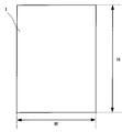
- FIG. 1 to 3 show an example of a niobium material.
- 1 is an external view
- FIG. 2 is a side view
- FIG. 3 is a top view.
- the niobium material 1 shown in FIG. 1 has a cylindrical shape.
- the thickness H and diameter W of the niobium material 1 are shown in FIG.
- the size of the niobium material 1 is not particularly limited, but is preferably, for example, 20 to 200 mm in thickness H and 100 to 300 mm in diameter W for easy handling.
- the niobium material 1 is highly purified, for example, by casting such as a melting method (also referred to as EB melting method) by an electron beam (EB), and has a niobium purity of 99.5% or more, that is, 99.5% by mass or more. It is preferable to have a composition containing This is because the niobium purity of the sputtering target conforms to the niobium purity of the niobium material.
- a melting method also referred to as EB melting method
- EB electron beam
- niobium material 1 A niobium material having a composition containing at least 2% niobium is used.
- the processing is performed in a first forging step, a first heat treatment step, a second forging step, a second heat treatment step, a cold rolling step, and a third heat treatment step. And.
- first forging two or more sets of first kneading forging are performed.
- cold forging also referred to as first cold forging
- a process having a cold forging process also referred to as a second cold forging process
- the direction parallel to the thickness direction is the thickness H direction in FIG. 2, and the direction perpendicular to the thickness direction is the diameter W direction in FIG.
- the number of times of the first kneading forging is two to four (two sets to four sets).
- the first press forging is preferably cold forging.
- hot forging is performed, surface cracking may occur due to oxidation.
- crystal grain growth occurs, a fine crystal structure with an average crystal grain size of 250 ⁇ m or less may not be obtained.
- the average Vickers hardness Hv of the niobium material 1 after the first forging step is preferably 100 or more.
- the measurement of the Vickers hardness Hv is performed, for example, according to JIS Z 2244: 2009 "Vickers hardness test-test method".
- the pressure applied in the direction of the diameter W does not have to be always constant, and it is preferable to change the direction halfway.
- pressure is applied to the pressure application direction 2 which is one of the diameter W directions
- the pressure application direction is changed by applying pressure in a pressure application direction 3 which is a direction perpendicular to the pressure application direction 2 along the upper surface of the. It is also effective to change the direction in which pressure is applied during one set of first twist forging.
- the niobium material 1 is recrystallized by performing the first heat treatment after the first forging step.
- the first heat treatment is performed, for example, at a temperature of 1300 ° C. or more.
- the internal strain generated in the niobium material 1 in the first forging process can be removed by the first heat treatment process, and the niobium material 1 can be further recrystallized to obtain a uniform fine crystal structure.
- the heat treatment temperature is preferably 1350 to 1500 ° C., for example, and the heat treatment time is preferably 5 to 15 hours. If the heat treatment temperature exceeds 1500 ° C. or the heat treatment time exceeds 15 hours, grain growth may occur.
- the heat treatment conditions are preferably, for example, 1350 to 1400 ° C. ⁇ 5 to 10 hours.
- the heat treatment atmosphere is preferably a vacuum atmosphere of 0.133 Pa or less. In an oxygen-containing atmosphere, the surface may be oxidized during heat treatment.
- one or more sets of second kneading forging are performed after the first heat treatment step.
- cold forging also referred to as third cold forging
- a process having a cold forging process also referred to as a fourth cold forging process
- one set of second kneading forging is referred to as one set of second kneading forging.
- the details of the second twist forging are the same as those of the first twist forging, but the number of times for the second twist forging may be at least one set, for example, 1 to 4 sets. Is preferred.
- the pressure direction is changed by applying pressure in the pressure application direction 3 which is a direction perpendicular to the pressure application direction 2 along the upper surface of the niobium material 1 Is preferred.
- the second forging step is preferably cold forging as described above.
- the second kneading forging can further promote the reduction of the crystal grain size.
- the niobium material 1 is recrystallized by performing a second heat treatment after the second forging step.
- the second heat treatment is performed, for example, at a temperature of 1300 ° C. or more.
- the heat treatment temperature is preferably 1350 to 1500 ° C.
- the heat treatment time is preferably 5 to 15 hours. If the heat treatment temperature exceeds 1500 ° C. or the heat treatment time exceeds 15 hours, grain growth may occur.
- the heat treatment conditions are preferably, for example, 1350 to 1400 ° C. ⁇ 5 to 10 hours.
- the heat treatment atmosphere is preferably a vacuum atmosphere of 0.133 Pa or less. In an oxygen-containing atmosphere, the surface may be oxidized during heat treatment.
- cold rolling is performed once or more on the niobium material 1.
- the cold rolling step is a step of plastically working the niobium material 1 into a plate shape.
- cold rolling may be performed twice or more as necessary. It is desirable to process the niobium material 1 so as to have a thickness of 20 mm or less, preferably 10 to 15 mm, by a cold rolling process. Furthermore, cutting is performed after the cold rolling process to adjust the thickness of the sputtering target.
- the processing rates of the first forging process, the second forging process, and the cold rolling process are arbitrary. Machining ratio of niobium material 1, ie, reduction of area and thickness in cold forging (per set) or cold rolling in at least one of the first forging step, the second forging step, and the cold rolling step Preferably, at least one of the reduction rates is 30% or more.
- the cross-sectional reduction rate is a reduction rate of the cross-sectional area in the diameter W direction of the niobium material 1.
- the thickness reduction rate is the reduction rate in the thickness H direction of the niobium material 1.
- the processing rate of 30% or more at this time is the processing rate per set.
- the process which has a processing rate of 30% or more is a cold process.
- the first forging process ⁇ the first heat treatment process ⁇ the second forging process ⁇ the second heat treatment process even if cold rolling with a working ratio of 30% or more is performed, internal strain It is easy to control the occurrence.
- the processing rate is low, the occurrence of internal strain can be suppressed.
- production takes too much time. Therefore, it is preferable to perform a process with a processing rate of 30% or more.
- the upper limit of the processing rate of one process is 80% or less. If the niobium material 1 is processed at a processing rate of more than 80% in one process, internal strain, cracks, wrinkles and the like are easily generated, and further, after heat treatment, crystals of the sputtered surface are easily oriented to (200) plane, random orientation The crystal structure of Furthermore, if the niobium material 1 is processed at a working ratio of more than 70% in cold rolling, the crystal of the sputtered surface is easily oriented to the (200) plane after heat treatment, and the crystal structure of random orientation is lost. Therefore, it is preferable that the upper limit of the processing rate of a rolling process is 70% or less.
- the working ratio is more preferably 30% or more.
- the processing rate in the case of performing two or more sets of forging kneaded shows the processing rate of the forging knead for 1 set.
- at least one of the cross-section reduction rate or the thickness reduction rate may be set to 30% or more.
- the working ratio of each of the first and second forging steps is more preferably 40 to 80%, and the working ratio of the cold rolling step is more preferably 40 to 70%.
- the niobium material 1 is recrystallized by performing the third heat treatment after the cold rolling step.
- the third heat treatment is performed, for example, at a temperature of 1100 ° C. or higher.
- the heat treatment conditions are preferably, for example, 1150 to 1250 ° C. ⁇ 3 to 6 hours.
- the heat treatment atmosphere is preferably a vacuum atmosphere of 0.133 Pa or less. In an oxygen-containing atmosphere, the surface may be oxidized during heat treatment.
- the internal strain generated in the niobium material 1 by the cold rolling process can be removed and the niobium material 1 can be recrystallized.
- the shape of the niobium material 1 is adjusted by cutting such as lathing, if necessary. Further, the backing plate is bonded to the niobium material 1 by diffusion bonding. Thus, the sputtering target can be manufactured.
- the sputtering target which made the fine crystal structure of 250 micrometers or less of average crystal grain size and the crystal structure of random orientation make compatible can be manufactured.
- a high purity niobium material for example, a sputtering target having a composition containing 99.5% by mass or more of niobium, a purity of 99.5% or more, and a crystal structure of a microcrystalline structure and a random crystal orientation. You can get it.
- the thickness of the sputtering target is preferably, for example, 6 mm or more.
- the measurement of the average grain size is performed, for example, by taking a magnified image of a unit area of 500 ⁇ m ⁇ 500 ⁇ m by an optical micrograph and using a line intercept method.
- a line intercept method an arbitrary straight line (length 500 ⁇ m) is drawn, the number of Nb crystal grain sizes on the line is counted, and the average grain size is determined by (500 ⁇ m / number of crystals on 500 ⁇ m straight line). An average value obtained by performing this work three times is taken as an average crystal grain size.
- the surface and the inside of the sputtering target of the embodiment have a randomly oriented crystal structure.
- the crystal structure of random orientation is provided so as to be maintained over the entire thickness direction.
- the crystal structure of the said random orientation is identified, for example using a X-ray diffraction (X-Ray Diffraction (XRD) method).
- X-ray diffraction measurement X-ray diffraction measurement
- X-ray diffraction measurement is performed under the conditions of a Cu target, a tube voltage of 40 kV, a tube current of 40 mA, a scattering slit of 0.63 mm, and a light receiving slit of 0.15 mm.
- the X-ray diffraction pattern obtained by X-ray diffraction measurement (2 ⁇ ) of the sputtering surface (surface) of the sputtering target has a first peak attributable to the (110) plane of the crystal and a first peak attributable to the (211) plane of the crystal. 2 and the third peak attributable to the (200) plane of the crystal.
- the peak intensity of the second peak is lower than the peak intensity of the first peak
- the peak intensity of the third peak is lower than the peak intensity of the second peak. That is, the relative intensities of the peaks of the (110) plane, the (211) plane, and the (200) plane decrease in the order of (110) plane> (211) plane> (200) plane.
- the crystal structure is oriented not in random orientation but in a specific crystal orientation, the relative intensity ratio of each surface is shifted.
- peaks belonging to the (220) plane, the (310) plane, and the (222) plane are also detected, but in order to judge whether or not the random orientation is made, the (110) plane, the (211) plane, It is important to compare the intensities of the peaks attributed to the (200) plane. The reason is that the peaks belonging to these planes are main peaks having high intensity in the powder diffraction file (PDF) data.
- PDF powder diffraction file
- the first peak has a relative intensity of 100
- the second peak has a relative intensity of 17 or more and 44 or less
- the third peak has a relative intensity of 13 or more and 35 or less. That is, when the peak intensity of the (110) plane is 100, the peak intensity of the (211) plane is in the range of 17 to 44, and the peak intensity of the (200) plane is in the range of 13 to 35.
- the crystal structure is oriented not in random orientation but in a specific crystal orientation, the relative intensity ratio of each surface is shifted.
- an X-ray diffraction pattern obtained by X-ray diffraction measurement (2 ⁇ ) of the inside in the depth direction of the target, ie, the thickness direction of the sputtering target Similarly to the above-described surface includes a first peak, a second peak, and a third peak. That is, the relative intensities of the peaks of the (110) plane, the (211) plane, and the (200) plane decrease in the order of (110) plane> (211) plane> (200) plane, similarly to the sputtered surface.
- the presence or absence of ghost grain can also be determined by the above-mentioned X-ray diffraction measurement.
- ghost grain When ghost grain is present, a portion in which the magnitude relationship of peak intensities is not “(110) plane> (211) plane> (200) plane” is formed.
- the grain boundary of the Nb crystal is blurred.
- the crystal structure of the random orientation of the sputtering surface is maintained along the thickness direction. For this reason, even if sputtering is performed for a long time using a sputtering target having a thickness of 10 mm or more, a change in sputtering rate is unlikely to occur, and sputtering characteristics with high reliability are exhibited. In addition, even if the sputtering target is a large sputtering target having a diameter of 300 mm or more, the crystal structure having an average crystal grain size of 250 ⁇ m or less and a uniform random orientation can be maintained. Therefore, it is possible to obtain a uniform state in which the Vickers hardness Hv of the surface of the sputtering target is in the range of 60 to 120 and the variation of the Vickers hardness Hv is 30% or less.
- the manufacturing method of the semiconductor element of embodiment has the process of sputtering using a sputtering target.
- the sputtering target of the above embodiment is used as a sputtering target.
- the method of manufacturing a semiconductor device includes the step of forming a film containing niobium by performing sputtering using the sputtering target.
- Niobium is used as a barrier film of a semiconductor element as niobium nitride (NbN). For this reason, it is preferable to perform a sputtering process in nitrogen-containing atmosphere. With the sputtering target of the embodiment, the reliability in long-term sputtering is high, so the reliability of the semiconductor element can be improved.
- Examples 1 to 5 Comparative Examples 1 to 2
- a columnar niobium material high purity niobium billet containing at least 99.95 mass% of niobium having a diameter of W100 to 300 mm and a thickness H of 100 to 200 mm was prepared, and the manufacturing process shown in Table 1 was performed.
- a processing rate (%) of Table 1 the larger value was described among the cross-section reduction rate (%) of diameter W direction, and the thickness reduction rate (%) of thickness H direction.
- the above-mentioned processing rate is the processing rate per one time (one set) of each process, and the working rate was the same as the processing rate of the first set for the example where the number of times (set number) is 2 or more .
- the niobium raw material which passed through the manufacturing process of Table 1 was lathe-processed, and the sputtering target of the target size shown in Table 2 was obtained.
- the average crystal grain size ( ⁇ m) in each target and the presence or absence of random orientation were confirmed.
- the sputtering target according to this example exhibits highly reliable sputtering characteristics. Therefore, the reliability of the semiconductor element can be improved.
- a sputtering target of the embodiment it is possible to manufacture a sputtering target having stable sputtering characteristics.
- the reliability of the semiconductor element can be improved.
- the residue after sputtering can be reduced, and the cost for reuse can also be reduced.
Landscapes
- Chemical & Material Sciences (AREA)
- Engineering & Computer Science (AREA)
- Materials Engineering (AREA)
- Mechanical Engineering (AREA)
- Metallurgy (AREA)
- Organic Chemistry (AREA)
- Chemical Kinetics & Catalysis (AREA)
- Physical Vapour Deposition (AREA)
- Forging (AREA)
- Electrodes Of Semiconductors (AREA)
Abstract
平均結晶粒径250μm以下の微細結晶構造を有し、均一なランダム配向を具備するスパッタリングターゲットを提供する。2セット以上の第1のこねくり鍛造を行う第1の鍛造工程と、第1の熱処理を行うことによりニオブ素材を再結晶化させる第1の熱処理工程と、第1の熱処理工程後に、1セット以上の第2のこねくり鍛造を行う第2の鍛造工程と、第2の熱処理を行うことによりニオブ素材を再結晶化させる第2の熱処理工程と、ニオブ素材に対し冷間圧延を1回以上行う冷間圧延工程と、第3の熱処理を行うことによりニオブ素材を再結晶化させる第3の熱処理工程と、を具備する。
Description
本発明の実施形態は、スパッタリングターゲット、およびスパッタリングターゲットの製造方法、ならびに半導体素子の製造方法に関する。
近年、半導体素子の高集積化に伴い、Al、Cuなどの金属配線幅を徐々に狭くすることが求められている。これに伴い、金属配線のエレクトロンマイグレーションを抑制すること、すなわちエレクトロマイグレーション特性の向上が要求されている。エレクトロマイグレーション特性を向上させるためには、例えば成膜後の配線用金属膜を金属結晶の最稠密面が柱状に成長するように結晶成長させることが望ましい。上記結晶成長のためには、例えば配線用金属膜の下に形成されるTiN、TaN、NbNなどのバリア膜も同様に最稠密面が柱状になるようにスパッタリングされることが望ましい。
Cu配線やAl配線を使う場合、バリア膜としてTaN(窒化タンタル)膜、NbN(窒化ニオブ)膜、TiN(窒化チタン)膜を用いることが好適である。TaN膜、NbN膜、TiN膜は、例えば高純度Taスパッタリングターゲット、高純度Nbスパッタリングターゲット、または高純度Tiスパッタリングターゲット等を用いて窒素雰囲気中でスパッタリングによる成膜を行うことにより形成される。スパッタリングにより、最稠密面が柱状になるようにバリア膜を成膜するためには、ターゲット金属の結晶粒径の微細化および結晶配向性のランダム化(ランダム配向)が必要である。さらに、膜の均一性を向上させるためには、鋳造組織の残存(ゴーストグレイン)という問題を解消しなければならない。
従来、Nbスパッタリングターゲットの製造において、インゴットに対して冷間で絞め鍛造を行った後、冷間で据え込み鍛造を行う。さらに、熱処理を行って冷間圧延を行うことが知られている。絞め鍛造は、円柱状インゴットの直径方向に圧力を加える加工である。また、据え込み鍛造は、絞め鍛造により長軸方向に伸びたインゴットを長軸方向に薄板にするための加工である。絞め鍛造および据え込み鍛造は、どちらも一定方向から圧力を掛けて塑性変形させる加工である。一定方向からの圧力のみによる塑性変形では、平均結晶粒径が微細になると結晶方位が特定の方位に配向しやすい。
さらに、上記の従来の工程では、微細な結晶構造を有するNbスパッタリングターゲットを製造したとき、スパッタ面(表面)に均一なランダム配向を有する結晶構造が得られたとしても、厚さ方向については必ずしも均一なランダム配向を有する結晶構造を得られない。このため、長時間スパッタリングを行うとスパッタレートのズレなどの不具合が生じ均一な膜が得られないといった問題がある。
実施形態の一態様は、平均結晶粒径250μm以下の微細結晶構造を有し、かつ均一なランダム配向の結晶構造を有するスパッタリングターゲットを提供することを目的としている。実施形態の一態様は、平均結晶粒径250μm以下の微細結晶構造を有し、かつ均一なランダム配向の結晶構造を有するスパッタリングターゲットの製造方法を提供することを目的としている。実施形態の一態様は、平均結晶粒径250μm以下の微細結晶構造を有し、かつ均一なランダム配向の結晶構造を有するスパッタリングターゲットを用いた半導体素子の製造方法を提供することを目的としている。
実施形態のスパッタリングターゲットの製造方法は、円柱形状を有するニオブ素材の加工を行うことによりスパッタリングターゲットを製造するスパッタリングターゲットの製造方法である。上記加工は、第1の鍛造工程、第1の熱処理工程、第2の鍛造工程、第2の熱処理工程、冷間圧延工程、および第3の熱処理工程を具備する。
第1の鍛造工程では、ニオブ素材の厚さ方向に平行な方向からニオブ素材に圧力を加えて行う冷間鍛造加工と、厚さ方向に垂直な方向からニオブ素材に圧力を加えて行う冷間鍛造加工とを有する加工を1セットの第1のこねくり鍛造としたとき、2セット以上の第1のこねくり鍛造を行う。第1の熱処理工程では、第1の鍛造工程後に、第1の熱処理を行うことによりニオブ素材を再結晶化させる。
第2の鍛造工程では、ニオブ素材の厚さ方向に平行な方向からニオブ素材に圧力を加えて行う冷間鍛造加工と、厚さ方向に垂直な方向からニオブ素材に圧力を加えて行う冷間鍛造加工とを有する加工を1セットの第2のこねくり鍛造としたとき、第1の熱処理工程後に、1セット以上の第2のこねくり鍛造を行う。第2の熱処理工程では、第2の鍛造工程後に、第2の熱処理を行うことによりニオブ素材を再結晶化させる。
冷間圧延工程では、第2の熱処理工程後に、ニオブ素材に対し冷間圧延を1回以上行う。第3の熱処理工程では、第3の熱処理を行うことによりニオブ素材を再結晶化させる。
実施形態のスパッタリングターゲットは、99.5質量%以上のニオブを含む組成と、250μm以下の平均結晶粒径を有する結晶を含む結晶構造と、を具備する。99.5質量%以上のニオブを含む組成を有するスパッタリングターゲットをニオブスパッタリングターゲットともいう。スパッタリングターゲットの表面のX線回折測定により得られるX線回折パターンは、結晶の(110)面に帰属する第1のピークと、結晶の(211)面に帰属し、かつ第1のピークのピーク強度よりも低いピーク強度を有する第2のピークと、結晶の(200)面に帰属し、かつ第2のピークのピーク強度よりも低いピーク強度を有する第3のピークとを含む。
実施形態の半導体素子の製造方法は、上記スパッタリングターゲットを用いてスパッタリングを行うことによりニオブを含む膜を成膜する工程を具備する。
以下、実施形態について説明する。
実施形態のスパッタリングターゲットの製造方法では、円柱形状のニオブインゴットまたは円柱形状のニオブビレットからなるニオブ素材の加工を行うことによりスパッタリングターゲットを製造する。
図1ないし図3は、ニオブ素材の一例を示す図である。図1は外観図であり、図2は側面図であり、図3は上面図である。図1に示すニオブ素材1は、円柱形状を具備する。ニオブ素材1の厚さH、直径Wを図2に示す。ニオブ素材1のサイズは、特に限定されないが、例えば20~200mmの厚さH、100~300mmの直径Wを有することにより、取扱いが容易になるため好ましい。
ニオブ素材1は、例えば電子ビーム(Electron Beam:EB)による溶解法(EB溶解法ともいう)などの鋳造により高純度化され、ニオブ純度99.5%以上、すなわち99.5質量%以上のニオブを含む組成を有することが好ましい。スパッタリングターゲットのニオブ純度がニオブ素材のニオブ純度に準ずるためである。例えば、ニオブ純度99.5%以上、すなわち99.5質量%以上のニオブを含む組成を有するスパッタリングターゲットが必要であるとき、ニオブ素材1として例えばニオブ純度99.5%以上、すなわち99.5質量%以上のニオブを含む組成を具備するニオブ素材が用いられる。
上記実施形態のスパッタリングターゲットの製造方法において、上記加工は、第1の鍛造工程、第1の熱処理工程、第2の鍛造工程、第2の熱処理工程、冷間圧延工程、および第3の熱処理工程と、を具備する。
第1の鍛造工程では、2セット以上の第1のこねくり鍛造を行う。このとき、ニオブ素材1の厚さ方向に平行な方向からニオブ素材1に圧力を加えて行う冷間鍛造加工(第1の冷間鍛造加工ともいう)と、厚さ方向に垂直な方向からニオブ素材1に圧力を加えて行う冷間鍛造加工(第2の冷間鍛造加工ともいう)とを有する加工を1セットの第1のこねくり鍛造とする。厚さ方向に平行な方向とは図2における厚さH方向のことであり、厚さ方向に垂直な方向とは図2における直径W方向のことである。
第1のこねくり鍛造では、異なる方向から圧力を加えることから、結晶粒径の微細化を達成し、特定の方向に結晶配向が偏ることを防ぐことができる。また、鋳造により製造されたニオブ素材1における鋳造組織の残存(ゴーストグレイン)を減少させることができる。第1のこねくり鍛造の回数(セット数)は多いほど良いが、回数が多すぎると製造コストが高くなり、また素材の割れ、シワなどが発生しやすくなる。よって、第1のこねくり鍛造の回数は2回~4回(2セット~4セット)であることが好ましい。
第1のこねくり鍛造は上記のとおり冷間鍛造であることが好ましい。熱間で鍛造を行うと酸化により表面割れが発生してしまうおそれがある。また、結晶の粒成長が起きるので、平均結晶粒径250μm以下の微細な結晶組織が得られないおそれがある。
第1の鍛造工程後のニオブ素材1のビッカース硬さHvの平均値は100以上であることが好ましい。第1のこねくり鍛造を2セット以上行うことにより組織の均質化が図られ、ニオブ素材1の硬度が高くなる。しかしながら、後述の製造工程を考慮したとき、ビッカース硬さHvの平均値を100未満にしたとしても、これ以上の効果は得られず、第1のこねくり鍛造工程を無駄に行うことになる。従って、第1のこねくり鍛造のセット数を制御する上でもビッカース硬さHvの平均値が100以上になるように第1のこねくり鍛造を行うことが好ましい。ビッカース硬さHvの測定は、例えばJIS Z2244:2009「ビッカース硬さ試験-試験方法」に準じて行われる。
直径W方向に加える圧力は、常に一定方向である必要はなく、途中で方向を変えることが好ましい。例えば、図3に示すように、1セット目の第1のこねくり鍛造では直径W方向の一つである圧力付加方向2に圧力を付加し、2セット目の第1のこねくり鍛造ではニオブ素材1の上面に沿って圧力付加方向2に垂直な方向である圧力付加方向3に圧力を付加することで、圧力を付加する方向を変えることが好ましい。なお、1セットの第1のこねくり鍛造中で圧力を付加する方向を変えることも有効である。また、直径W方向においても圧力を付加する方向を変えることにより、結晶粒径の微細化を達成し、特定の方向に結晶配向が偏ることを防ぐ効果をより得ることができる。
第1の熱処理工程では、第1の鍛造工程後に、第1の熱処理を行うことによりニオブ素材1を再結晶化させる。第1の熱処理工程では、例えば1300℃以上の温度で第1の熱処理を行う。
第1の熱処理工程により第1の鍛造工程でニオブ素材1に生じた内部歪を除去し、さらにニオブ素材1を再結晶化させて均一な微細結晶構造を得ることができる。熱処理温度は例えば1350~1500℃であることが好ましく、熱処理時間は例えば5~15時間であることが好ましい。熱処理温度が1500℃を超えるまたは熱処理時間が15時間を超えると粒成長を伴うおそれがある。熱処理条件は、例えば1350~1400℃×5~10時間であることが好ましい。熱処理雰囲気は0.133Pa以下の真空雰囲気であることが好ましい。酸素含有雰囲気では熱処理中に表面が酸化されるおそれがある。
第2の鍛造工程では、第1の熱処理工程後に、1セット以上の第2のこねくり鍛造を行う。このとき、ニオブ素材1の厚さ方向に平行な方向からニオブ素材1に圧力を加えて行う冷間鍛造加工(第3の冷間鍛造加工ともいう)と、厚さ方向に垂直な方向からニオブ素材1に圧力を加えて行う冷間鍛造加工(第4の冷間鍛造加工ともいう)とを有する加工を1セットの第2のこねくり鍛造とする。
第2の鍛造工程において、第2のこねくり鍛造の詳細は第1のこねくり鍛造と同様であるが、第2のこねくり鍛造の回数は1セット以上であればよく、例えば1~4セットであることが好ましい。2セット以上とする場合、セット毎に直径W方向に付加する圧力方向を変えることが好ましく、例えば図3に示したように、1セット目の第2のこねくり鍛造では圧力付加方向2に圧力を付加し、2セット目の第2のこねくり鍛造ではニオブ素材1の上面に沿って圧力付加方向2に垂直な方向である圧力付加方向3に圧力を付加することで、圧力を付加する方向を変えることが好ましい。第2の鍛造工程は、上記のとおり冷間鍛造であることが好ましい。第2のこねくり鍛造により、結晶粒径の微細化をより推進することができる。
第2の熱処理工程では、第2の鍛造工程後に第2の熱処理を行うことによりニオブ素材1を再結晶化させる。第2の熱処理工程では、例えば1300℃以上の温度で第2の熱処理を行う。
第2の熱処理工程により、第2の鍛造工程でニオブ素材1に生じた内部歪を除去し、さらにニオブ素材1を再結晶化させて均一な微細結晶構造を得ることができる。熱処理温度は1350~1500℃、熱処理時間は5~15時間であることが好ましい。熱処理温度が1500℃を超えるまたは熱処理時間が15時間を超えると粒成長を伴うおそれがある。熱処理条件は、例えば1350~1400℃×5~10時間であることが好ましい。熱処理雰囲気は0.133Pa以下の真空雰囲気であることが好ましい。酸素含有雰囲気では熱処理中に表面が酸化されるおそれがある。
冷間圧延工程では、ニオブ素材1に対し冷間圧延を1回以上行う。冷間圧延工程は、ニオブ素材1を板状に塑性加工する工程である。冷間圧延工程では、必要に応じ、冷間圧延を2回以上行ってもよい。冷間圧延工程により、20mm以下の厚さ、好ましくは10~15mmの厚さを有するようにニオブ素材1を加工することが望ましい。さらに、冷間圧延工程後に切削加工を施してスパッタリングターゲットの板厚を調整する。
第1の鍛造工程、第2の鍛造工程、および冷間圧延工程の加工率は任意である。第1の鍛造工程、第2の鍛造工程、および冷間圧延工程の少なくとも1つの工程におけるこねくり鍛造(1セットあたり)または冷間圧延において、ニオブ素材1の加工率、すなわち断面減少率および厚さ減少率の少なくとも一方は30%以上であることが好ましい。断面減少率は、ニオブ素材1の直径W方向の断面積の減少率である。厚さ減少率はニオブ素材1の厚さH方向の減少率である。なお、第1の鍛造工程では、第1のこねくり鍛造を2セット以上行っている。このときの30%以上の加工率とは、1セットあたりの加工率である。
30%以上の加工率を有する工程は、冷間工程であることが好ましい。例えば、第1の鍛造工程→第1の熱処理工程→第2の鍛造工程→第2の熱処理工程を行った後であると、加工率30%以上の冷間圧延を行ったとしても内部歪の発生を抑制しやすい。加工率が低いと内部歪の発生を抑制することができる。しかしながら、各工程を何度も繰り返すことになるため、製造に時間が掛り過ぎてしまう。よって、加工率30%以上の工程を行うことが好ましい。
なお、1つの工程の加工率の上限は80%以下であることが好ましい。一つの工程で80%を超える加工率でニオブ素材1を加工すると内部歪、割れ、シワなどが発生し易く、さらには熱処理後にスパッタ面の結晶が(200)面に配向し易くなり、ランダム配向の結晶構造ではなくなる。さらに、冷間圧延において70%を超える加工率でニオブ素材1を加工すると、熱処理後にスパッタ面の結晶が(200)面に配向し易くなり、ランダム配向の結晶構造ではなくなる。そのため、圧延工程の加工率の上限は70%以下であることが好ましい。
第1、第2の鍛造工程、および冷間圧延工程の全ての工程において、加工率は30%以上であることがより好ましい。なお、上記したようにこねくり鍛造を2セット以上行う場合の加工率とは、1セットあたりのこねくり鍛造の加工率を示す。加工率30%以上にするためには、例えば断面減少率または厚さ減少率の少なくとも一方を30%以上にすればよい。さらに、第1、第2の鍛造工程の加工率のそれぞれは40~80%であることがより好ましく、冷間圧延工程の加工率は、40~70%であることがより好ましい。
第3の熱処理工程では、冷間圧延工程後に、第3の熱処理を行うことによりニオブ素材1を再結晶化させる。第3の熱処理工程では、例えば1100℃以上の温度で第3の熱処理を行う。熱処理条件は、例えば1150~1250℃×3~6時間であることが好ましい。熱処理雰囲気は、0.133Pa以下の真空雰囲気であることが好ましい。酸素含有雰囲気では熱処理中に表面が酸化されるおそれがある。
第3の熱処理工程により、冷間圧延工程によりニオブ素材1に生じた内部歪を除去すると共に、ニオブ素材1を再結晶化させることができる。第3の熱処理工程後は、必要に応じ、旋盤加工などの切削加工によりニオブ素材1の形状を整える。また、拡散接合によりバッキングプレートをニオブ素材1に接合する。以上により、スパッタリングターゲットを製造することができる。
上記製造方法であれば、例えば平均結晶粒径250μm以下の微細な結晶構造とランダム配向の結晶構造とを両立させたスパッタリングターゲットを製造することができる。また、純度の高いニオブ素材を使うことにより、例えば、99.5質量%以上のニオブを含む組成と、純度99.5%以上で微細結晶構造とランダムな結晶配向の結晶構造を有するスパッタリングターゲットを得ることができる。また、鋳造組織の残存であるゴーストグレインが無い微細結晶構造を形成することができる。鋳造組織の残存であるゴーストグレインが存在すると、部分的にランダム配向ではない部分ができてしまう。スパッタリングターゲットの厚さは、たとえば6mm以上であることが好ましい。
平均結晶粒径の測定は、例えば光学顕微鏡写真により単位面積500μm×500μmの拡大写真を撮り、線インターセプト法を用いて行われる。線インターセプト法では、任意の直線(長さ500μm分)を引き、その線上にあるNb結晶粒径の数を数え、(500μm/直線500μm上の結晶の数)により平均の結晶粒径を求める。この作業を3回行った平均値を平均結晶粒径とする。
実施形態のスパッタリングターゲットの表面および内部は、ランダム配向の結晶構造を有することが好ましい。例えば、ランダム配向の結晶構造は、厚さ方向の全てに渡って維持されて設けられていることが好ましい。これにより、スパッタレートが変化することなくスパッタリングによる成膜を行うことができるため、成膜された膜の均一性を高めることができる。
上記ランダム配向の結晶構造は、例えばX線回折(X‐Ray Diffraction:XRD)法を用いて同定される。例えば、Cuターゲット、管電圧40kV、管電流40mA、散乱スリット0.63mm、受光スリット0.15mmの条件でX線回折法による測定(X線回折測定)を行う。
スパッタリングターゲットのスパッタ面(表面)のX線回折測定(2θ)により得られるX線回折パターンは、結晶の(110)面に帰属する第1のピークと、結晶の(211)面に帰属する第2のピーク、結晶の(200)面に帰属する第3のピークとを含む。
このとき、第2のピークのピーク強度は、第1のピークのピーク強度よりも低く、第3のピークのピーク強度は、第2のピークのピーク強度よりも低い。すなわち、(110)面、(211)面、(200)面の各面のピークの相対強度が(110)面>(211)面>(200)面の順で小さくなる。ランダム配向ではなく特定の結晶配向で配向された結晶構造を有しているとき、各面の相対強度比がずれる。
X線回折測定では、(220)面、(310)面、(222)面に帰属するピークも検出されるが、ランダム配向か否かを判断するには(110)面、(211)面、(200)面に帰属するピークの強度を比較することが重要である。その理由は、これらの面に帰属するピークがPDF(Powder Diffraction File)データにおいて、高い強度を有する主要なピークであるためである。
第1のピークは100の相対強度を有し、第2のピークは17以上44以下の相対強度を有し、第3のピークは13以上35以下の相対強度を有する。すなわち、(110)面のピーク強度を100としたときに、(211)面のピーク強度は17ないし44の範囲であり、(200)面のピーク強度は13ないし35の範囲である。ランダム配向ではなく特定の結晶配向で配向された結晶構造を有しているとき、各面の相対強度比がずれる。
ランダム配向がスパッタリングターゲットの厚さ方向における内部に渡って維持されているため、ターゲットの深さ方向、すなわちスパッタリングターゲットの厚さ方向における内部のX線回折測定(2θ)により得られるX線回折パターンは、上記表面と同様に第1のピークと、第2のピークと、第3のピークとを含む。すなわち、スパッタ面と同様に(110)面、(211)面、(200)面のピークの相対強度が(110)面>(211)面>(200)面の順に小さくなる。
さらに、上記X線回折測定によりゴーストグレインの有無も判定することができる。ゴーストグレインが存在するとピーク強度の大小関係が「(110)面>(211)面>(200)面」でない部分が形成される。また、光学顕微鏡(拡大写真)で組織写真を撮る場合、ゴーストグレインが存在すると、Nb結晶の粒界が不鮮明な組織がみられる。
実施形態のスパッタリングターゲットでは、厚さ方向に沿ってスパッタ面のランダム配向の結晶構造が維持されている。このため、10mm以上の厚さを有するスパッタリングターゲットを用いて長時間スパッタリングを行ったとしても、スパッタレートの変化が生じ難く、信頼性が高いスパッタリング特性を示す。また、スパッタ面の直径が300mm以上と大型のスパッタリングターゲットであっても、平均結晶粒径250μm以下かつ均質なランダム配向の結晶構造を維持できる。このため、スパッタリングターゲットの表面のビッカース硬さHvが60~120の範囲内であり、ビッカース硬さHvのばらつきが30%以下である均一な状態を得ることができる。
すなわち、直径300mm以上かつ厚さ10mm以上の大型スパッタリングターゲットにおいて、平均結晶粒径250μm以下かつスパッタ面の均質なランダム配向の結晶構造を厚さ方向に沿って維持することができる。その上でゴーストグレインの残存をなくすことができる。このため、成膜工程において長期間使用したとしてもスパッタレートの変化が生じにくくなり、スパッタリングターゲットの厚さが2mm程度になるまで安定したスパッタリングを提供することができる。使用後のスパッタリングターゲットは再利用されることが多い。通常、余ったターゲットを溶解して再度インゴットにして使う。ニオブは高融点金属であるため溶解するには高温炉が必要であり、コスト負荷の要因となる。このため、残余となるターゲット部分が少ない方が好ましい。
実施形態の半導体素子の製造方法は、スパッタリングターゲットを用いてスパッタリングする工程を有する。実施形態の半導体素子の製造方法では、スパッタリングターゲットとして上記実施形態のスパッタリングターゲットを用いる。
例えば、実施形態の半導体素子の製造方法は、上記スパッタリングターゲットを用いてスパッタリングを行うことによりニオブを含む膜を成膜する工程を具備する。
ニオブは、窒化ニオブ(NbN)として半導体素子のバリア膜に用いられる。このため、窒素含有雰囲気下でスパッタリング工程を行うことが好ましい。実施形態のスパッタリングターゲットであれば、長期間のスパッタリングにおける信頼性が高いことから、半導体素子の信頼性を向上させることができる。
(実施例1~5、比較例1~2)
直径W100~300mm×厚さH100~200mmの円柱状のニオブ素材(99.95質量%以上のニオブを含む高純度ニオブビレット)を用意し、表1に示す製造工程を施した。なお、表1の加工率(%)として、直径W方向の断面減少率(%)および厚さH方向の厚さ減少率(%)のうち、大きい方の値を記載した。上記加工率は、各工程の1回(1セット)あたりの加工率であり、回数(セット数)が2以上の実施例、比較例については1セット目の加工率と同様の加工率とした。また、回数(セット数)が2以上の実施例、比較例では、図3に示すように回毎(セット毎)に直径W方向における圧力付加方向を、第1の圧力付加方向とニオブ素材の上面に沿って第1の圧力付加方向に垂直な第2の圧力付加方向とに交互に変更して各工程を行った。また、表1には、第1の鍛造工程後のニオブ素材のビッカース硬さHvの平均値を示す。
直径W100~300mm×厚さH100~200mmの円柱状のニオブ素材(99.95質量%以上のニオブを含む高純度ニオブビレット)を用意し、表1に示す製造工程を施した。なお、表1の加工率(%)として、直径W方向の断面減少率(%)および厚さH方向の厚さ減少率(%)のうち、大きい方の値を記載した。上記加工率は、各工程の1回(1セット)あたりの加工率であり、回数(セット数)が2以上の実施例、比較例については1セット目の加工率と同様の加工率とした。また、回数(セット数)が2以上の実施例、比較例では、図3に示すように回毎(セット毎)に直径W方向における圧力付加方向を、第1の圧力付加方向とニオブ素材の上面に沿って第1の圧力付加方向に垂直な第2の圧力付加方向とに交互に変更して各工程を行った。また、表1には、第1の鍛造工程後のニオブ素材のビッカース硬さHvの平均値を示す。

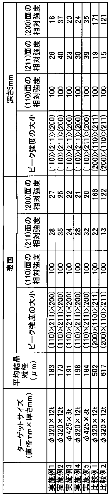
表1の製造工程を経たニオブ素材を旋盤加工して、表2に示すターゲットサイズのスパッタリングターゲットを得た。各ターゲットにおける平均結晶粒径(μm)、ランダム配向の有無を確認した。
スパッタ面および断面から単位面積500μm×500μmの拡大写真(光学顕微鏡写真)を撮り、線インターセプト法(3本の直線の平均値)により平均結晶粒径を求めた。スパッタ面およびスパッタ面から厚さ方向に深さ5mmまで掘ったところから任意の測定箇所を選択し、X線回折測定(2θ)によりランダム配向の結晶構造の有無を判定した。X線Cu-Kα(ターゲットCu)、管電圧40kV、電流40mA、散乱スリット0.63mm、受光スリット0.15mmで上記X線回折測定を行った。結晶組織はいずれも再結晶化されていた。結果を表2に示す。
次に、各実施例または比較例に係るスパッタリングターゲットに拡散接合によりバッキングプレートを接合した後、窒素雰囲気中でスパッタリングによる成膜を行った。そのとき、スパッタリング後のエロージョン面のゴーストグレインの有無を確認した。結果を表3に示す。
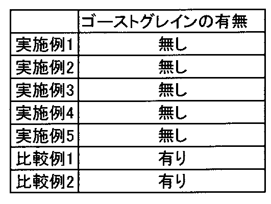
表2および表3から、本実施例に係るスパッタリングターゲットでは、スパッタリング後のエロージョン面に鋳造組織の残留物であるゴーストグレインが発見されず、安定したスパッタリング特性を示すことがわかる。これに対し、比較例に係るスパッタリングターゲットでは、ゴーストグレインが発見された。これは鋳造組織が残存し、スパッタ面のランダム配向がスパッタリングターゲットの厚さ方向に渡って維持されていないためである。
この結果、本実施例に係るスパッタリングターゲットは、信頼性が高いスパッタリング特性を示すことがわかる。このため、半導体素子の信頼性を向上させることが可能となる。
本発明のいくつかの実施形態を説明したが、これらの実施形態は、例として提示したものであり、発明の範囲を限定することは意図していない。これら新規な実施形態は、その他の様々な形態で実施されることが可能であり、発明の要旨を逸脱しない範囲で、種々の省略、置き換え、変更を行うことができる。これら実施形態やその変形は、発明の範囲や要旨に含まれるとともに、特許請求の範囲に記載された発明とその均等の範囲に含まれる。
実施形態のスパッタリングターゲットの製造方法によれば、安定したスパッタリング特性を有するスパッタリングターゲットを製造することができる。上記スパッタリングターゲットを用いて半導体素子を製造することにより、半導体素子の信頼性を向上させることができる。また、スパッタリング後の残余を少なくすることができ、再利用のためのコストも低減することができる。
Claims (15)
- 円柱形状を有するニオブ素材の加工を行うことによりスパッタリングターゲットを製造するスパッタリングターゲットの製造方法であって、
前記加工は、
前記ニオブ素材の厚さ方向に平行な方向から前記ニオブ素材に圧力を加えて行う第1の冷間鍛造加工と、前記厚さ方向に垂直な方向から前記ニオブ素材に圧力を加えて行う第2の冷間鍛造加工とを有する加工を1セットの第1のこねくり鍛造としたとき、2セット以上の前記第1のこねくり鍛造を行う第1の鍛造工程と、
前記第1の鍛造工程後に、第1の熱処理を行うことにより前記ニオブ素材を再結晶化させる第1の熱処理工程と、
前記ニオブ素材の厚さ方向に平行な方向から前記ニオブ素材に圧力を加えて行う第3の冷間鍛造加工と、前記厚さ方向に垂直な方向から前記ニオブ素材に圧力を加えて行う第4の冷間鍛造加工とを有する加工を1セットの第2のこねくり鍛造としたとき、前記第1の熱処理工程後に、1セット以上の前記第2のこねくり鍛造を行う第2の鍛造工程と、
前記第2の鍛造工程後に、第2の熱処理を行うことにより前記ニオブ素材を再結晶化させる第2の熱処理工程と、
前記第2の熱処理工程後に、前記ニオブ素材に対し冷間圧延を1回以上行う冷間圧延工程と、
前記冷間圧延工程後に、第3の熱処理を行うことにより前記ニオブ素材を再結晶化させる第3の熱処理工程と、を具備する、スパッタリングターゲットの製造方法。 - 1300℃以上の温度で前記第1の熱処理を行い、
1300℃以上の温度で前記第2の熱処理を行い、
1100℃以上の温度で前記第3の熱処理を行う、請求項1記載のスパッタリングターゲットの製造方法。 - 0.133Pa以下の真空雰囲気下で前記第1の熱処理、前記第2の熱処理、および前記第3の熱処理を行う、請求項1記載のスパッタリングターゲットの製造方法。
- 1セットの前記第1のこねくり鍛造および前記第2のこねくり鍛造の少なくとも一方による、前記ニオブ素材の加工率が30%以上80%未満である、請求項1記載のスパッタリングターゲットの製造方法。
- 前記冷間圧延工程において、2回以上の前記冷間圧延を行い、
1回あたりの前記冷間圧延による、前記ニオブ素材の加工率が30%以上70%未満である、請求項1記載のスパッタリングターゲットの製造方法。 - 前記第1の鍛造工程後の前記ニオブ素材のビッカース硬さの平均値は、100以上である、請求項1記載のスパッタリングターゲットの製造方法。
- 前記ニオブ素材は、99.5質量%以上のニオブを含む、請求項1記載のスパッタリングターゲットの製造方法。
- 99.5質量%以上のニオブを含む組成と、
250μm以下の平均結晶粒径を有する結晶を含む結晶構造と、を具備するスパッタリングターゲットであって、
前記スパッタリングターゲットの表面のX線回折測定により得られるX線回折パターンは、前記結晶の(110)面に帰属する第1のピークと、前記結晶の(211)面に帰属し、かつ前記第1のピークのピーク強度よりも低いピーク強度を有する第2のピークと、前記結晶の(200)面に帰属し、かつ前記第2のピークのピーク強度よりも低いピーク強度を有する第3のピークとを含む、スパッタリングターゲット。 - 前記スパッタリングターゲットの厚さ方向における内部のX線回折測定により得られるX線回折パターンは、前記第1のピークと、前記第2のピークと、前記第3のピークとを含む、請求項8記載のスパッタリングターゲット。
- 前記スパッタリングターゲットの表面および内部は、ランダム配向の前記結晶構造を有する、請求項9記載のスパッタリングターゲット。
- 前記第1のピークは、100の第1の相対強度を有し、
前記第2のピークは、17以上44以下の第2の相対強度を有し、
前記第3のピークは、13以上35以下の第3の相対強度を有する、請求項8記載のスパッタリングターゲット。 - 6mm以上の厚さを有する、請求項8記載のスパッタリングターゲット。
- 前記スパッタリングターゲットのビッカース硬さのばらつきは、30%以下である、請求項8記載のスパッタリングターゲット。
- 請求項8記載のスパッタリングターゲットを用いてスパッタリングを行うことによりニオブを含む膜を成膜する工程を具備する、半導体素子の製造方法。
- 窒素含有雰囲気下で前記スパッタリングを行う、請求項14記載の半導体素子の製造方法。
Priority Applications (1)
| Application Number | Priority Date | Filing Date | Title |
|---|---|---|---|
| JP2015544800A JP6599234B2 (ja) | 2013-10-29 | 2014-10-28 | スパッタリングターゲットおよびその製造方法、ならびに半導体素子の製造方法 |
Applications Claiming Priority (2)
| Application Number | Priority Date | Filing Date | Title |
|---|---|---|---|
| JP2013224656 | 2013-10-29 | ||
| JP2013-224656 | 2013-10-29 |
Publications (1)
| Publication Number | Publication Date |
|---|---|
| WO2015064087A1 true WO2015064087A1 (ja) | 2015-05-07 |
Family
ID=53003715
Family Applications (1)
| Application Number | Title | Priority Date | Filing Date |
|---|---|---|---|
| PCT/JP2014/005444 Ceased WO2015064087A1 (ja) | 2013-10-29 | 2014-10-28 | スパッタリングターゲットおよびその製造方法、ならびに半導体素子の製造方法 |
Country Status (2)
| Country | Link |
|---|---|
| JP (2) | JP6599234B2 (ja) |
| WO (1) | WO2015064087A1 (ja) |
Cited By (5)
| Publication number | Priority date | Publication date | Assignee | Title |
|---|---|---|---|---|
| CN110241392A (zh) * | 2019-07-16 | 2019-09-17 | 宁波江丰电子材料股份有限公司 | 一种靶材及提高靶材利用率的方法与应用 |
| CN111197148A (zh) * | 2018-11-20 | 2020-05-26 | 宁波江丰电子材料股份有限公司 | 靶材的制作方法 |
| US10858759B2 (en) | 2016-02-26 | 2020-12-08 | A.L.M.T. Corp. | Molybdenum crucible |
| CN116555713A (zh) * | 2023-05-08 | 2023-08-08 | 先导薄膜材料(安徽)有限公司 | 一种钒靶晶粒细化方法 |
| CN117444114A (zh) * | 2023-11-03 | 2024-01-26 | 先导薄膜材料(安徽)有限公司 | 一种改善晶粒大小均匀性的金属靶材的制备方法 |
Citations (8)
| Publication number | Priority date | Publication date | Assignee | Title |
|---|---|---|---|---|
| JP2003171759A (ja) * | 2001-12-03 | 2003-06-20 | Toshiba Corp | スパッタリングターゲット |
| JP2004244664A (ja) * | 2003-02-12 | 2004-09-02 | Toshiba Corp | スパッタリングターゲットとその製造方法 |
| JP2007077507A (ja) * | 2006-10-30 | 2007-03-29 | Toshiba Corp | スパッタリングターゲットの製造方法 |
| JP2007302996A (ja) * | 2006-04-13 | 2007-11-22 | Ulvac Material Kk | Taスパッタリングターゲットおよびその製造方法 |
| JP2008240112A (ja) * | 2007-03-28 | 2008-10-09 | Toshiba Corp | マグネトロンスパッタリング装置および半導体装置の製造方法 |
| JP2009108412A (ja) * | 2008-11-10 | 2009-05-21 | Nikko Kinzoku Kk | ターゲット |
| JP2009528922A (ja) * | 2006-03-07 | 2009-08-13 | キャボット コーポレイション | 変形させた金属部材の製造方法 |
| WO2011111373A1 (ja) * | 2010-03-11 | 2011-09-15 | 株式会社 東芝 | スパッタリングターゲットとその製造方法、および半導体素子の製造方法 |
Family Cites Families (3)
| Publication number | Priority date | Publication date | Assignee | Title |
|---|---|---|---|---|
| JP2001295035A (ja) * | 2000-04-11 | 2001-10-26 | Toshiba Corp | スパッタリングターゲットおよびその製造方法 |
| JP4351483B2 (ja) * | 2003-06-24 | 2009-10-28 | 大同特殊鋼株式会社 | Nbスパッタリングターゲット及びその製造方法 |
| JP5951599B2 (ja) * | 2011-04-18 | 2016-07-13 | 株式会社東芝 | 高純度Niスパッタリングターゲットおよびその製造方法 |
-
2014
- 2014-10-28 JP JP2015544800A patent/JP6599234B2/ja active Active
- 2014-10-28 WO PCT/JP2014/005444 patent/WO2015064087A1/ja not_active Ceased
-
2019
- 2019-08-07 JP JP2019145501A patent/JP6721769B2/ja active Active
Patent Citations (8)
| Publication number | Priority date | Publication date | Assignee | Title |
|---|---|---|---|---|
| JP2003171759A (ja) * | 2001-12-03 | 2003-06-20 | Toshiba Corp | スパッタリングターゲット |
| JP2004244664A (ja) * | 2003-02-12 | 2004-09-02 | Toshiba Corp | スパッタリングターゲットとその製造方法 |
| JP2009528922A (ja) * | 2006-03-07 | 2009-08-13 | キャボット コーポレイション | 変形させた金属部材の製造方法 |
| JP2007302996A (ja) * | 2006-04-13 | 2007-11-22 | Ulvac Material Kk | Taスパッタリングターゲットおよびその製造方法 |
| JP2007077507A (ja) * | 2006-10-30 | 2007-03-29 | Toshiba Corp | スパッタリングターゲットの製造方法 |
| JP2008240112A (ja) * | 2007-03-28 | 2008-10-09 | Toshiba Corp | マグネトロンスパッタリング装置および半導体装置の製造方法 |
| JP2009108412A (ja) * | 2008-11-10 | 2009-05-21 | Nikko Kinzoku Kk | ターゲット |
| WO2011111373A1 (ja) * | 2010-03-11 | 2011-09-15 | 株式会社 東芝 | スパッタリングターゲットとその製造方法、および半導体素子の製造方法 |
Cited By (7)
| Publication number | Priority date | Publication date | Assignee | Title |
|---|---|---|---|---|
| US10858759B2 (en) | 2016-02-26 | 2020-12-08 | A.L.M.T. Corp. | Molybdenum crucible |
| CN111197148A (zh) * | 2018-11-20 | 2020-05-26 | 宁波江丰电子材料股份有限公司 | 靶材的制作方法 |
| CN111197148B (zh) * | 2018-11-20 | 2021-11-19 | 宁波江丰电子材料股份有限公司 | 靶材的制作方法 |
| CN110241392A (zh) * | 2019-07-16 | 2019-09-17 | 宁波江丰电子材料股份有限公司 | 一种靶材及提高靶材利用率的方法与应用 |
| CN110241392B (zh) * | 2019-07-16 | 2021-08-17 | 宁波江丰电子材料股份有限公司 | 一种靶材及提高靶材利用率的方法与应用 |
| CN116555713A (zh) * | 2023-05-08 | 2023-08-08 | 先导薄膜材料(安徽)有限公司 | 一种钒靶晶粒细化方法 |
| CN117444114A (zh) * | 2023-11-03 | 2024-01-26 | 先导薄膜材料(安徽)有限公司 | 一种改善晶粒大小均匀性的金属靶材的制备方法 |
Also Published As
| Publication number | Publication date |
|---|---|
| JP6599234B2 (ja) | 2019-10-30 |
| JPWO2015064087A1 (ja) | 2017-03-09 |
| JP2020007640A (ja) | 2020-01-16 |
| JP6721769B2 (ja) | 2020-07-15 |
Similar Documents
| Publication | Publication Date | Title |
|---|---|---|
| JP5714506B2 (ja) | タンタルスパッタリングターゲットおよびタンタルスパッタリングターゲットの製造方法ならびに半導体素子の製造方法 | |
| JP6721769B2 (ja) | スパッタリングターゲットおよび半導体素子の製造方法 | |
| USRE47788E1 (en) | Sputtering target, manufacturing method thereof, and manufacturing method of semiconductor element | |
| KR102134781B1 (ko) | 스퍼터링 타깃의 제조 방법 및 스퍼터링 타깃 | |
| JP5905600B2 (ja) | タンタルスパッタリングターゲット及びその製造方法 | |
| TWI695894B (zh) | 濺鍍用鈦靶及其製造方法、以及含鈦薄膜的製造方法 | |
| WO2012057057A1 (ja) | スパッタリング用チタンターゲット | |
| WO2014097900A1 (ja) | タンタルスパッタリングターゲット及びその製造方法 | |
| TWI707046B (zh) | 鉭濺鍍靶及其製造方法 | |
| CN107532287B (zh) | 钽溅射靶及其制造方法 | |
| TW202018098A (zh) | 濺鍍靶及其製造方法 | |
| JP6871301B2 (ja) | スパッタリングターゲット、窒化チタン膜の製造方法、および半導体素子の製造方法 | |
| JP6595188B2 (ja) | スパッタリングターゲットの製造方法 |
Legal Events
| Date | Code | Title | Description |
|---|---|---|---|
| 121 | Ep: the epo has been informed by wipo that ep was designated in this application |
Ref document number: 14857350 Country of ref document: EP Kind code of ref document: A1 |
|
| ENP | Entry into the national phase |
Ref document number: 2015544800 Country of ref document: JP Kind code of ref document: A |
|
| NENP | Non-entry into the national phase |
Ref country code: DE |
|
| 122 | Ep: pct application non-entry in european phase |
Ref document number: 14857350 Country of ref document: EP Kind code of ref document: A1 |