WO2015053095A1 - 光走査装置及び画像形成装置 - Google Patents
光走査装置及び画像形成装置 Download PDFInfo
- Publication number
- WO2015053095A1 WO2015053095A1 PCT/JP2014/075589 JP2014075589W WO2015053095A1 WO 2015053095 A1 WO2015053095 A1 WO 2015053095A1 JP 2014075589 W JP2014075589 W JP 2014075589W WO 2015053095 A1 WO2015053095 A1 WO 2015053095A1
- Authority
- WO
- WIPO (PCT)
- Prior art keywords
- cover
- optical
- light beam
- polygon mirror
- light
- Prior art date
- Legal status (The legal status is an assumption and is not a legal conclusion. Google has not performed a legal analysis and makes no representation as to the accuracy of the status listed.)
- Ceased
Links
Images

Classifications
-
- G—PHYSICS
- G03—PHOTOGRAPHY; CINEMATOGRAPHY; ANALOGOUS TECHNIQUES USING WAVES OTHER THAN OPTICAL WAVES; ELECTROGRAPHY; HOLOGRAPHY
- G03G—ELECTROGRAPHY; ELECTROPHOTOGRAPHY; MAGNETOGRAPHY
- G03G15/00—Apparatus for electrographic processes using a charge pattern
- G03G15/04—Apparatus for electrographic processes using a charge pattern for exposing, i.e. imagewise exposure by optically projecting the original image on a photoconductive recording material
- G03G15/043—Apparatus for electrographic processes using a charge pattern for exposing, i.e. imagewise exposure by optically projecting the original image on a photoconductive recording material with means for controlling illumination or exposure
-
- G—PHYSICS
- G02—OPTICS
- G02B—OPTICAL ELEMENTS, SYSTEMS OR APPARATUS
- G02B26/00—Optical devices or arrangements for the control of light using movable or deformable optical elements
- G02B26/08—Optical devices or arrangements for the control of light using movable or deformable optical elements for controlling the direction of light
- G02B26/10—Scanning systems
- G02B26/12—Scanning systems using multifaceted mirrors
-
- H—ELECTRICITY
- H04—ELECTRIC COMMUNICATION TECHNIQUE
- H04N—PICTORIAL COMMUNICATION, e.g. TELEVISION
- H04N1/00—Scanning, transmission or reproduction of documents or the like, e.g. facsimile transmission; Details thereof
- H04N1/04—Scanning arrangements, i.e. arrangements for the displacement of active reading or reproducing elements relative to the original or reproducing medium, or vice versa
- H04N1/06—Scanning arrangements, i.e. arrangements for the displacement of active reading or reproducing elements relative to the original or reproducing medium, or vice versa using cylindrical picture-bearing surfaces, i.e. scanning a main-scanning line substantially perpendicular to the axis and lying in a curved cylindrical surface
-
- H—ELECTRICITY
- H04—ELECTRIC COMMUNICATION TECHNIQUE
- H04N—PICTORIAL COMMUNICATION, e.g. TELEVISION
- H04N1/00—Scanning, transmission or reproduction of documents or the like, e.g. facsimile transmission; Details thereof
- H04N1/04—Scanning arrangements, i.e. arrangements for the displacement of active reading or reproducing elements relative to the original or reproducing medium, or vice versa
- H04N1/113—Scanning arrangements, i.e. arrangements for the displacement of active reading or reproducing elements relative to the original or reproducing medium, or vice versa using oscillating or rotating mirrors
-
- H—ELECTRICITY
- H04—ELECTRIC COMMUNICATION TECHNIQUE
- H04N—PICTORIAL COMMUNICATION, e.g. TELEVISION
- H04N2201/00—Indexing scheme relating to scanning, transmission or reproduction of documents or the like, and to details thereof
- H04N2201/0077—Types of the still picture apparatus
- H04N2201/0082—Image hardcopy reproducer
Definitions
- the present invention relates to an optical scanning device mounted on an electrophotographic image forming apparatus such as a copying machine, a printer, and a facsimile, and an image forming apparatus mounting the optical scanning device.
- An electrophotographic image forming apparatus such as a laser beam printer or a digital copying machine is provided with an optical scanning device for exposing a photosensitive member.
- the light scanning device scans a photosensitive member by deflecting a light beam emitted from a semiconductor laser by a rotating polygon mirror that rotates the light beam.
- an electrostatic latent image is formed on the photosensitive member, and toner is attached to the electrostatic latent image and developed to form a toner image, which is transferred to a sheet to form an image.
- the rotary polygon mirror may be rotated at high speed as one means.
- a high negative pressure is generated inside the light scanning device centering on the vicinity of the rotary polygon mirror, and air can be easily sucked from the outside of the light scanning device.
- the air outside the optical scanning device may be mixed with very fine dust and dirt, and grease volatiles used in the image forming apparatus itself. When such air penetrates the inside of the optical scanning device, adhesion to the reflecting surface of the rotating polygon mirror progresses in several weeks to several months, and the light quantity of exposure decreases, and an image such as an extremely thin density partially appears May cause failure.
- the cover of the optical box is provided with a seal member having elasticity made of synthetic rubber, polyurethane or the like at a joint portion in contact with the outer peripheral edge of the optical box.
- a seal member having elasticity made of synthetic rubber, polyurethane or the like at a joint portion in contact with the outer peripheral edge of the optical box.
- Patent Document 1 for example, the assembling process is performed by forming the seal member made of elastomer integrally with the optical box or the cover instead of attaching the seal member of a separate part.
- the assembling process is performed by forming the seal member made of elastomer integrally with the optical box or the cover instead of attaching the seal member of a separate part.
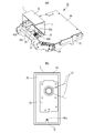
- FIG. 7A is a perspective view showing the appearance of the light scanning device 21 described later.
- the optical scanning device 21 includes an optical box 20 and a cover 30 which covers the open surface of the optical box.
- the optical box 20 integrally holds therein a rotating polygon mirror, various lenses, a folding mirror, and the like, which will be described later.
- the cover 30 covers the open surface of the optical box 20 and seals the inside of the optical box 20. The details of the light scanning device 21 will be described later.
- the cover 30 has a seal portion formed by injection molding in order to ensure the airtightness inside the optical box 20.
- the gate portion 31a for filling the melting material forming the seal portion is required.
- the injection molding is performed so as to protrude from the gate portion 31a.
- the runner portion 31c in the shape of the injection nozzle of the machine remains. Therefore, depending on the position where the gate portion 31a is provided, as shown in FIG.
- the runner portion 31c blocks the optical path of the synchronous light incident on the synchronous sensor, causing malfunction of the optical scanning device or the photosensitive member. There is a concern that an image defect may occur. In addition, when the runner portion 31c contacts the folding mirror or the lens, the lens or the like is pushed away and shifted, and there is a concern that the irradiation position of the light beam to the photosensitive body is largely shifted. As a result, in order to prevent this, there has been a problem that an extra work process such as cutting the runner portion 31c protruding from the gate portion 31a is required.
- the present invention has been made under such circumstances, and it is an object of the present invention to injection-mold a seal portion with a simple configuration that does not require complicated assembly operations.
- the present invention is configured as follows.
- An optical scanning device comprising: an optical member for guiding light to the photosensitive member; an optical box for accommodating the light source, the rotary polygon mirror, and the optical member; and a cover for covering an opening of the optical box A dustproof member sandwiched between the cover and the side wall of the optical box and molded on the cover to dustproof the inside of the optical box, a gate unit for injecting the melted dustproof member, and the gate unit A flow path through which the melted dust-proof member injected from the side flows, and by attaching the cover to the optical box, the dust-proof member is sandwiched between the side wall and the cover. It has a channel formed on over the said gate portion includes an optical scanning device, characterized in that provided as viewed from a direction of a rotation axis of the rotary
- An optical scanning device comprising: an optical member for guiding light to the photosensitive member; an optical box for accommodating the light source, the rotary polygon mirror, and the optical member; and a cover for covering an opening of the optical box A dustproof member sandwiched between the cover and the side wall of the optical box and molded on the cover to dustproof the inside of the optical box, a gate unit for injecting the melted dustproof member, and the gate unit A flow path through which the melted dust-proof member injected from the side flows, and by attaching the cover to the optical box, the dust-proof member is sandwiched between the side wall and the cover.
- the gate portion is located at a position where the virtual normal extending from the gate portion to the cover does not intersect the optical path region of the light beam in the optical box
- An optical scanning device comprising: an optical member for guiding light to the photosensitive member; an optical box for containing the light source, the rotary polygon mirror, and the optical member; and a cover for covering the opening of the optical box
- the box has a wall standing from the bottom so as to surround the rotary polygon mirror installed at the bottom of the optical box, the cover is an opening surrounded by the wall, and the rotary polygon mirror
- the first cover comprising A dustproof member sandwiched between the first cover and the erected wall and formed on the first cover to dustproof the inside of the optical box, and
- An optical scanning device comprising: an optical member for guiding light to the photosensitive member; an optical box for containing the light source, the rotary polygon mirror, and the optical member; and a cover for covering the opening of the optical box
- the box has a wall standing from the bottom so as to surround the rotary polygon mirror installed at the bottom of the optical box, the cover is an opening surrounded by the wall, and the rotary polygon mirror A first cover covering a first opening through which the rotary polygon mirror passes when the light source is installed at the bottom, and a second cover covering a second opening which is the opening of the optical box excluding the first opening A cover, the first cover comprising A dustproof member sandwiched between the first cover and the erected wall and formed on the first cover to dustproof the inside of the optical box,
- the seal portion can be injection-molded with a simple configuration that does not require a complicated assembly operation.
- Schematic cross-sectional view of the image forming apparatus of Example 1 The perspective view which shows the structure of the optical scanning device of Example 1, 2, and sectional drawing of an optical scanning device The figure explaining the cover composition of Example 1, a gate part The figure which explains the gate section arrangement territory of execution example 1
- Schematic cross-sectional view of the image forming apparatus of Example 2 The perspective view which shows the structure of the optical scanning device of Example 2, the figure explaining a cover structure, and a gate part
- the rotational axis direction of the rotary polygon mirror 203 described later is the Z axis direction
- the main scanning direction which is the scanning direction of the light beam or the longitudinal direction of the reflecting mirror is perpendicular to the X axis direction
- X axis and Z axis Direction is taken as the Y-axis direction.
- FIG. 1 is a schematic cross-sectional view of an electrophotographic image forming apparatus 100 according to the first embodiment.
- the image forming apparatus 100 illustrated in FIG. 1 includes four image forming units 101Y, 101M, 101C, and 101Bk that form toner images of yellow (Y), magenta (M), cyan (C), and black (Bk), respectively. Equipped with Hereinafter, the symbols Y, M, C, and Bk representing the respective colors are omitted unless necessary.
- the image forming unit 101 includes photosensitive drums 102 which are photosensitive members.
- Each image forming unit also includes a charging device 103 for charging the photosensitive drum 102 and a developing device 104 for developing the electrostatic latent image on the photosensitive drum with toner. Furthermore, each image forming unit includes a cleaning device 111 that removes the toner remaining on the photosensitive drum from the photosensitive drum (on the photosensitive member).
- Each image forming unit constitutes a process cartridge in which the photosensitive drum 102, the charging device 103, the developing device 104, and the cleaning device 111 described above are integrated.
- the process cartridge is a replaceable unit that can be attached to and detached from the image forming apparatus 100.
- the image forming units 101Y, 101M, 101C, and 101Bk will be referred to as process cartridges 101Y, 101M, 101C, and 101Bk.
- the main body of the image forming apparatus 100 is provided with an optical scanning device 21, transfer rollers 105 Y, 105 M, 105 C, 105 Bk, an intermediate transfer belt 106, a paper feed unit 109, a paper discharge unit 110, a transfer roller 107, and a fixing device 108.
- the intermediate transfer belt 106 rotates in the arrow direction (counterclockwise direction) in the drawing.
- the optical scanning device 21 is disposed below the photosensitive drums 102 in the direction of gravity (in the direction of the ⁇ Z axis).
- the optical scanning device 21 may be arranged to expose the photosensitive drum 102 from the upper side in the direction of gravity (the + Z-axis direction).
- the light scanning device 21 emits light beams LY, LM, LC, and LBk for exposing the photosensitive drums 102Y, 102M, 102C, and 102Bk charged by the charging devices 103Y, 103M, 103C, and 103Bk, respectively.
- electrostatic latent images are formed on the photosensitive drums 102Y, 102M, 102C, and 102Bk.
- the developing device 104 ⁇ / b> Y develops the electrostatic latent image formed on the photosensitive drum 102 ⁇ / b> Y with yellow toner.
- the developing device 104M develops the electrostatic latent image formed on the photosensitive drum 102M with magenta toner.
- the developing device 104C develops the electrostatic latent image formed on the photosensitive drum 102C with cyan toner.
- the developing device 104Bk develops the electrostatic latent image formed on the photosensitive drum 102Bk with black toner.
- the yellow toner image formed on the photosensitive drum 102Y is transferred to the intermediate transfer belt 106, which is an intermediate transfer member, by the transfer roller 105Y at the transfer portion Ty.
- the cleaning device 111Y collects the toner remaining on the photosensitive drum 102Y without being transferred to the intermediate transfer belt 106 between the transfer portion Ty in the rotational direction of the photosensitive drum 102Y and the charging portion of the charging device 103Y.
- the magenta toner image formed on the photosensitive drum 102M is transferred to the intermediate transfer belt 106 by the transfer roller 105M at the transfer portion Tm.
- the cleaning device 111M collects toner remaining on the photosensitive drum 102M without being transferred to the intermediate transfer belt 106 between the transfer portion Tm in the rotational direction of the photosensitive drum 102M and the charging portion of the charging device 103M.
- the cyan toner image formed on the photosensitive drum 102C is transferred to the intermediate transfer belt 106 by the transfer roller 105C at the transfer portion Tc.
- the cleaning device 111C collects the toner remaining on the photosensitive drum 102C without being transferred to the intermediate transfer belt 106 between the transfer portion Tc in the rotational direction of the photosensitive drum 102C and the charging portion of the charging device 103C.
- the black toner image formed on the photosensitive drum 102Bk is transferred to the intermediate transfer belt 106 by the transfer roller 105Bk at the transfer portion TBk.
- the cleaning device 111Bk collects the toner remaining on the photosensitive drum 102Bk without being transferred to the intermediate transfer belt 106 between the transfer portion TBk in the rotational direction of the photosensitive drum 102Bk and the charging portion of the charging device 103Bk.
- the cleaning device 111 of the present embodiment is provided with a blade that contacts the photosensitive drum 102, and the residual toner is collected by scraping off the toner remaining on the photosensitive drum by the blade.
- the toner images of the respective colors transferred onto the intermediate transfer belt 106 are transferred by the transfer roller 107 onto the recording sheet conveyed from the sheet feeding unit 109 at the transfer portion T2.
- the toner image transferred onto the recording sheet at the transfer unit T2 is subjected to a fixing process by the fixing device 108, and is discharged to the sheet discharge unit 110 after the fixing process.
- the above-described image forming apparatus 100 forms an image forming apparatus for monochrome image forming apparatus having one photosensitive drum, or directly forms a toner image formed on a plurality of photosensitive drums onto a recording medium. It may be an apparatus.
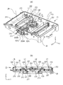
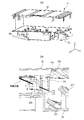
- FIG. 2A is a perspective view showing the configuration of the light scanning device 21, and FIG. 2B is a cross-sectional view of the light scanning device 21.
- light source units 202Y, 202M, 202C, 202Bk are attached to the outer wall of the optical box 20 of the light scanning device 21.
- the light source unit 202Y emits a light beam LY for exposing the photosensitive drum 102Y
- the light source unit 202M emits a light beam LM for exposing the photosensitive drum 102M
- the light source unit 202C emits a light beam LC for exposing the photosensitive drum 102C
- the light source unit 202Bk emits a light beam LBk for exposing the photosensitive drum 102Bk.
- the light source units 202Y, 202M, 202C, 202Bk are arranged close to each other.
- a plane crossing the rotating polygon mirror 203 with the rotation axis of the rotating polygon mirror 203 as a normal is defined as a virtual plane.
- the light beam LY emitted from the light source unit 202Y and the light beam LBk emitted from the light source unit 202Bk have an optical path obliquely incident from the upper side in the direction of gravity (+ Z axis direction) with respect to the virtual plane. It is incident on the reflective surface.
- the light beam LC emitted from the light source unit 202C and the light beam LM emitted from the light source unit 202M have an optical path obliquely incident from the lower side in the direction of gravity (-Z-axis direction) to the virtual plane described above.
- the light is incident on the reflecting surface of the rotating polygon mirror 203.
- a rotary polygon mirror 203 having four reflecting surfaces is provided at the center of the optical box 20. As shown in FIG. At the time of image formation, the rotary polygon mirror 203 rotates the rotation axis shown by the dotted line in FIG. 2A in the R1 direction.
- the light beam LY emitted from the light source unit 202Y is incident on the reflecting surface of the rotating polygon mirror 203.
- the light beam LY is deflected (reflected) to the side A shown in FIG. 2A by the reflecting surface of the rotating polygon mirror 203.
- the light beam LM emitted from the light source unit 202M is incident on the same reflection surface as the reflection surface of the rotary polygon mirror 203 on which the light beam LY is incident.
- the light beam LM is deflected by the reflecting surface of the rotating polygon mirror 203 to the same side (A side) as the light beam LY.
- the light beam LBk emitted from the light source unit 202Bk is incident on a reflection surface different from the reflection surface on which the light beams LY and LM are incident.
- the light beam LBk is deflected to the B side shown in FIG. 2A by the reflecting surface of the rotating polygon mirror 203.
- the light beam LC emitted from the light source unit 202C is incident on the same reflection surface as the reflection surface of the rotary polygon mirror 203 on which the light beam LBk is incident.
- the light beam LC is deflected to the same side (B side) as the light beam LBk by the reflection surface of the rotating polygon mirror 203.
- the light beams LY and LM deflected by the rotary polygon mirror 203 become light beams moving in the + X direction. That is, by being deflected by the rotating polygon mirror 203, the light beam LY becomes a light beam scanning the photosensitive drum 102Y in the + X direction, and the light beam LM becomes a light beam scanning the photosensitive drum 102M in the + X direction.
- the light beams LBk and LC deflected by the rotating polygon mirror 203 become light beams moving in the ⁇ X direction. That is, by being deflected by the rotating polygon mirror 203, the light beam LBk becomes a light beam for scanning the photosensitive drum 102Bk in the -X direction, and the light beam LC is a light beam for scanning the photosensitive drum 102C in the -X direction. Become.
- the optical paths of the light beams LY, LM, LC, and LBk deflected by the rotary polygon mirror 203 will be described with reference to FIG. 2B.
- the optical members of the present invention are accommodated and installed at the bottom (bottom) of the optical box 20.
- a rotary polygon mirror 203, each lens described above, and a cover 30 for dustproofing each reflection mirror are attached to an opening which is an open surface at the top of the optical box 20.
- the light beam LY deflected by the rotary polygon mirror 203 passes through the lens 206 and the lens 207 and then enters the reflection mirror 212.
- the reflection mirror 212 reflects the incident light beam LY toward the photosensitive drum 102Y.
- the cover 30 is formed with an opening 219 through which the light beam LY reflected by the reflection mirror 212 passes.
- the opening 219 is closed by a dustproof window 223 which is a transparent transparent window for passing the light beam LY.
- the light beam LY passing through the dustproof window 223 forms an image on the photosensitive drum 102Y.
- the light beam LM deflected by the rotating polygon mirror 203 passes through the lens 206 and then enters the reflection mirror 213.
- the reflection mirror 213 reflects the incident light beam LM toward the reflection mirror 214.
- the light beam LM reflected by the reflection mirror 213 passes through the lens 208 and enters the reflection mirror 214.
- the reflection mirror 214 reflects the incident light beam LM toward the photosensitive drum 102M.
- the cover 30 is formed with an opening 220 through which the light beam LM reflected by the reflection mirror 214 passes.
- the opening 220 is closed by a transparent dustproof window 224 through which the light beam LM passes.
- the light beam LM passing through the dustproof window 224 forms an image on the photosensitive drum 102M.
- the light beam LBk deflected by the rotating polygon mirror 203 is incident on the reflecting mirror 215 after passing through the lens 209 and the lens 210.
- the reflection mirror 215 reflects the incident light beam LBk toward the photosensitive drum 102Bk.
- the cover 30 is formed with an opening 222 through which the light beam LBk reflected by the reflection mirror 215 passes.
- the opening 222 is closed by a transparent dustproof window 226 which allows the light beam LBk to pass.
- the light beam LBk that has passed through the dustproof window 226 forms an image on the photosensitive drum 102Bk.
- the light beam LC deflected by the rotating polygon mirror 203 passes through the lens 209 and then enters the reflecting mirror 216.
- the reflection mirror 216 reflects the incident light beam LC toward the reflection mirror 217.
- the light beam LC reflected by the reflection mirror 216 passes through the lens 211 and enters the reflection mirror 217.
- the reflection mirror 217 reflects the incident light beam LC toward the photosensitive drum 102C.
- the cover 30 is formed with an opening 221 through which the light beam LC reflected by the reflection mirror 217 passes.
- the opening 221 is closed by a transparent dustproof window 225 through which the light beam LC passes.
- the light beam LC that has passed through the dustproof window 225 forms an image on the photosensitive drum 102C.
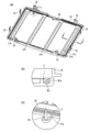
- FIG. 3A is a view showing the configuration of the cover 30 in the present embodiment, and is a perspective view of the cover 30 as viewed from the optical box 20 side.
- the cover 30 is provided with a plurality of hook portions 32 constituting a snap-fit structure by engaging a protrusion provided on the outer wall of the optical box 20.
- dustproof windows 223, 224, 225 and 226 are provided in the cover 30.
- a seal portion 31 which is a dustproof member is formed on the cover 30 by injection molding around the entire circumference that faces the outer peripheral edge formed by the side wall of the optical box 20 when attached to the optical box 20.
- the gate portion 31a for injecting a molten hot melt adhesive (hereinafter referred to as "hot melt") of a polyolefin type which is a molded member is two places in FIG. It is provided at a position that divides the entire length into almost two halves.
- the gate portions 31a are provided in two places in this embodiment, but may be increased or decreased according to the actual formability, and at least one or more places may be provided.
- FIG. 3B is a JJ cross-sectional view of the cover 30 cut at the position of JJ (one-dot chain line) indicated by a white arrow shown in FIG.
- FIG. 6 is a cross-sectional view showing the relationship of a portion 31.
- the cover 30 is provided with a groove 30a through which the melted hot melt injected from the gate 31a flows, and the seal 30 is formed by filling the groove 30a with the hot melt. Be done.
- the groove portion 30 a is formed such that the seal portion 31 is sandwiched between the side wall of the optical box 20 and the cover 30 by attaching the cover 30 to the optical box 20. Furthermore, in the groove 30a, a narrower anchor groove 30c having a smaller width and a smaller depth is provided, and the contact area between the cover 30 and the seal portion 31 is enlarged. Thus, the adhesion between the cover 30 and the seal portion 31 is secured so that the seal member, which is a dustproof member, does not unintentionally peel off from the cover 30. In addition, a concave groove is formed on the surface of the seal portion 31, and the outer peripheral edge formed by the side wall of the optical box 20 is inserted into the groove, thereby dustproofing the inside of the optical box 20 Sealing of 20 is also secured.
- FIG.3 (c) is the figure which expanded the part (gate part 31a peripheral part) of the cover 30 enclosed with the circle in FIG. 3 (a).
- the seal portion 31 is formed by injection molding, hot melt is injected from the gate portion 31a through an injection nozzle. Therefore, as shown in FIG. 3C, after the injection of the hot melt is completed, the molding material remaining in the injection nozzle is solidified as it is, and the runner portion 31c having a nozzle shape is formed in the gate portion 31a. .
- the runner portion 31c blocks the optical path of the light beam in the optical box 20, or the optical unit disposed in the optical box 20. There is a possibility that the position or position of the optical component may be changed by coming into contact with the component.
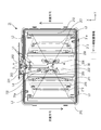
- FIG. 4 is a view of the optical scanning device 21 of this embodiment as viewed from the lower side (-Z-axis direction), except for the optical box 20, and the optical components disposed inside the cover 30 and the optical scanning device 21 It is the figure which showed the lens, the reflective mirror, etc. etc.
- light beams emitted from the light source units 202 pass through the incident light path L1 and enter the rotating polygon mirror (not shown in FIG. 4) driven by the polygon motor 232.
- the light source units 202 disposed on the A side are the light source units 202Y and 202M described above
- the light source units 202 disposed on the B side are the light source units 202C and 202Bk described above.
- the light beam incident on the rotary polygon mirror that rotates in the arrow direction is deflected to the reflection mirrors 212 and 215 along the scanning light path L2 or L3.
- the scanning direction indicates the direction in which the light beam deflected by the rotating polygon mirror is scanned.
- the light beams emitted from the light source units 202Y and 202M are deflected to the side A in the drawing (rightward in the drawing).
- the scanning light path L2 indicates the scanning light path to the reflection mirror 212 of the light beam emitted from the light source unit 202Y.
- the light beams emitted from the light source units 202C and 202Bk are deflected to the side B in the drawing (the left direction in the drawing).
- the scanning light path L3 indicates the scanning light path to the reflection mirror 215 of the light beam emitted from the light source unit 202Bk.
- the scanning light path L2 indicates the light path at the start of scanning of the light beam toward the reflecting mirror 212 and at the end of scanning.
- the scanning light path L3 indicates the light path at the start of scanning of the light beam toward the reflecting mirror 215 and at the end of scanning.
- the light beam emitted from the light source unit 202 is deflected by the rotary polygon mirror (not shown in FIG. 4), and the synchronization sensor 231 is transmitted via the anamorphic lens 230 along the synchronization light path L4. Make it incident.
- the synchronization sensor 231 generates, based on the timing of the incident light beam, a synchronization signal that indicates a scan start timing for irradiating the light beam from the light source unit 202.
- the other reference numerals in FIG. 4 are described in FIG. 2 and thus the description thereof is omitted here.
- optical components (lenses 206 to 211, reflection mirrors 212, 213, 215, 216, etc.), mechanical components for fixing the lenses and mirrors, etc. are installed inside the light scanning device 21.
- electrical components such as a polygon motor 232 and a synchronous sensor 231 are installed inside the light scanning device 21, and in the space inside the light scanning device 21, an incident light path L 1 through which a light beam passes and scanning light paths L 2 and L 3 , Synchronous light path L4.
- the optical paths L1 to L4 are indicated by two solid lines, respectively, and the light beam passes through an optical path region which is a space occupied by the two solid lines.
- the scanning light paths L2 and L3 indicate the largest light paths in the light scanning device 21, which is the space occupied by the scanning light paths.
- a gate portion arrangement region there is a region surrounded by a broken line in which neither a component nor an optical path exists, which is referred to as a “gate portion arrangement region”.
- the gate portion 31a is formed at a position where the virtual normal extending from the gate portion 31a to the cover 30 perpendicularly does not intersect the optical path region of the light beam in the optical box 20. Therefore, when the gate portion 31a is provided in the gate portion arrangement region, the light path is blocked by the runner portion 31c formed in the gate portion 31a, or the runner portion 31c contacts the component to change the posture. There will be no more.
- reflecting mirrors for example, reflecting mirrors 212 and 215
- scanning lenses for example, lenses 207 and 210
- X-axis direction the scanning direction of the scanning optical system.
- a reflection mirror and a scanning lens are arranged in the vicinity of the outer peripheral edge (short side in the figure) of the optical box 20 parallel to the scanning direction (X-axis direction)
- the area in which the gate portion is disposed is an area other than the side parallel to the scanning direction (X-axis direction) of the light scanning device 21, that is, the outer peripheral side (long side) of the side in the direction (Y-axis direction) orthogonal to the scanning direction. It is preferable to provide it on the side).
- the process of affixing a separate seal member on a cover can be eliminated by providing the seal part 31 integrally with the cover 30 by injection molding, and the additional process of cutting the runner part 31c of the seal part 31
- the work process also becomes unnecessary.
- the process of producing the cover with the seal member is simplified, and the cost of parts can be reduced.
- the shape of the seal portion 31 becomes constant, it is possible to stably ensure good sealing.
- each gate in the case of providing a plurality of gate portions 31 a so as to divide the entire flow path substantially equally.
- the seal portion can be injection-molded with a simple configuration that does not require a complicated assembly operation.
- a negative pressure may be generated inside the device by the rotation of the polygon motor, and air outside the optical scanning device may be easily sucked into the device. Therefore, there is also an optical scanning device of a configuration in which the portion on which the polygon motor is mounted in the optical scanning device is an independent space by a partition or the like.
- a gate portion arrangement region of a cover in the case of sealing a space in which a polygon motor is installed with a cover sealed by a seal member will be described.
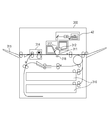
- FIG. 5 is a view showing a schematic configuration of a laser beam printer 300.
- the laser beam printer 300 is a monochrome image forming apparatus having one photosensitive drum.
- the laser beam printer 300 includes a photosensitive drum 311 on which an electrostatic latent image is formed by the light scanning device 42, a charging device 317 for uniformly charging the photosensitive drum 311, and a toner on the electrostatic latent image formed on the photosensitive drum 311.
- the laser beam printer 300 includes a controller (not shown) that controls an image forming operation by the image forming unit and a conveyance operation of the recording sheet.
- FIG. 6A is a perspective view showing the appearance of the optical scanning device 42 of this embodiment.
- the optical box 33 has a first opening which is an open surface formed by partition walls 43a, 43b, 43c and 43d described later, and a second opening which is an open surface of the optical box excluding the first opening. doing. Then, the optical box 33 is sealed by the cover 34 which is the first opening and the cover 35 which is the second opening.
- C indicates the upper portion of the cover 35
- D indicates the lower portion of the cover 35.
- the space sealed by the cover 35 is a space surrounded by partition walls 43a, 43b, 43c and 43d, which are formed integrally with the optical box 33 in the optical scanning device 42.
- the partition walls 43a, 43b, 43c and 43d are provided to stand from the bottom of the optical box 33, and adjacent partition walls are connected. Further, the partition wall 43a is provided with an opening 39 through which the light beam passes.
- a polygon motor 36 and a rotary polygon mirror 37 rotationally driven by the polygon motor 36 are mounted on the bottom of the optical box 33 surrounded by the partition walls 43a, 43b, 43c and 43d.
- the light beam emitted from the light source unit 38 is reflected by a reflection mirror (not shown) provided inside the light scanning device 42 sealed by the cover 34, and then enters the rotary polygon mirror 37 through the opening 39. (Indicated by a broken arrow in the figure). Then, the light beam that has entered the rotary polygon mirror 37 is deflected, and again enters the side sealed by the cover 34 through the opening 39.
- FIG. 6A a cover 35 is provided which covers only the open surface of the upper part of the independent space in which the polygon motor 36 is mounted on the bottom surface.
- FIG. 6B is a view looking up the cover 35 from the polygon motor 36 side (the bottom side of the optical scanning device 42), so that the positional relationship with the seal portion 40 formed on the outer peripheral edge of the cover 35 can be understood.
- the outer shape of the polygon motor 36 is overlapped.
- the scanning light path L5 (indicated by broken lines) shows the light path of the light beam (reflected light) reflected and deflected by the light beam incident on the rotating polygon mirror 37, and is occupied by two broken lines. A light beam passes through an optical path area which is space.
- the cover 35 has a seal portion 40, a gate portion 40a, and a flow path through which the melted hot melt injected from the gate portion 40a flows.
- the seal portion 40 is a dustproof member which is sandwiched between the cover 35 and the partition walls 43a, 43b, 43c, 43d and is formed on the cover 35 in order to dustproof the inside of the optical box.
- the gate portion 40 a is used to inject a molten hot melt to form the seal portion 40.
- the seal portion 40 is formed so as to be sandwiched between the partition walls 43 a, 43 b, 43 c, 43 d and the cover 35. Be done.
- the seal portion 40 is injection molded on the entire circumference along the edge of the cover 35, and the gate portion 40a for the molding is provided.
- the gate portion 40a is in the optical box 33 surrounded by the imaginary normal line extending perpendicularly to the cover 35 from the gate portion 40a and the partition walls 43a to 43d. It is formed in the position which does not cross with the optical path area
- the seal portion 40 integrally with the cover 35 by injection molding, the step of attaching a separate seal member to the cover can be eliminated, and the step of cutting the runner portion of the seal portion 40 is also performed. It becomes unnecessary. As a result, the process of producing the cover with the seal member is simplified, and the cost of parts can be reduced. Furthermore, as an effect of molding, since the shape of the seal portion 40 becomes constant, good sealing performance can be ensured.
- the cover 34 as in the first embodiment, the optical member installed inside the optical box 33 covered by the cover 34, the incident light path through which the light beam passes, the scanning light path and the synchronous light path The same effect as that of the first embodiment can be obtained by providing. As described above, according to this embodiment, the seal portion can be injection-molded with a simple configuration that does not require a complicated assembly operation.
Landscapes
- Physics & Mathematics (AREA)
- Engineering & Computer Science (AREA)
- Multimedia (AREA)
- Signal Processing (AREA)
- General Physics & Mathematics (AREA)
- Optics & Photonics (AREA)
- Mechanical Optical Scanning Systems (AREA)
- Facsimile Scanning Arrangements (AREA)
- Laser Beam Printer (AREA)
Priority Applications (3)
| Application Number | Priority Date | Filing Date | Title |
|---|---|---|---|
| US15/027,417 US10409190B2 (en) | 2013-10-09 | 2014-09-26 | Optical scanning device and image forming apparatus |
| CN201910177913.3A CN109901287B (zh) | 2013-10-09 | 2014-09-26 | 光学扫描设备和图像形成装置 |
| CN201480055496.0A CN105612455A (zh) | 2013-10-09 | 2014-09-26 | 光学扫描设备和图像形成装置 |
Applications Claiming Priority (2)
| Application Number | Priority Date | Filing Date | Title |
|---|---|---|---|
| JP2013212157A JP6242142B2 (ja) | 2013-10-09 | 2013-10-09 | 光走査装置及び画像形成装置 |
| JP2013-212157 | 2013-10-09 |
Publications (1)
| Publication Number | Publication Date |
|---|---|
| WO2015053095A1 true WO2015053095A1 (ja) | 2015-04-16 |
Family
ID=52812914
Family Applications (1)
| Application Number | Title | Priority Date | Filing Date |
|---|---|---|---|
| PCT/JP2014/075589 Ceased WO2015053095A1 (ja) | 2013-10-09 | 2014-09-26 | 光走査装置及び画像形成装置 |
Country Status (4)
| Country | Link |
|---|---|
| US (1) | US10409190B2 (enExample) |
| JP (1) | JP6242142B2 (enExample) |
| CN (2) | CN105612455A (enExample) |
| WO (1) | WO2015053095A1 (enExample) |
Families Citing this family (8)
| Publication number | Priority date | Publication date | Assignee | Title |
|---|---|---|---|---|
| JP6576158B2 (ja) * | 2015-08-19 | 2019-09-18 | キヤノン株式会社 | 光走査装置及び画像形成装置 |
| JP6608225B2 (ja) * | 2015-09-08 | 2019-11-20 | キヤノン株式会社 | 光走査装置 |
| JP6840562B2 (ja) * | 2017-02-15 | 2021-03-10 | キヤノン株式会社 | 光走査装置及び画像形成装置 |
| JP7423229B2 (ja) * | 2019-09-13 | 2024-01-29 | キヤノン株式会社 | 光学走査装置及びこれを搭載する画像形成装置 |
| JP7598556B2 (ja) | 2021-03-12 | 2024-12-12 | 株式会社リコー | 筐体構造、光走査装置及び画像形成装置 |
| JP7602959B2 (ja) | 2021-04-27 | 2024-12-19 | シャープ株式会社 | ハウジングカバー、光学箱および画像形成装置 |
| US12088765B2 (en) | 2022-03-22 | 2024-09-10 | Ricoh Company, Ltd. | Casing structure, optical scanner, and image forming apparatus |
| CN116859690B (zh) * | 2023-07-10 | 2024-08-02 | 虎丘影像(苏州)股份有限公司 | 一种曝光装置 |
Citations (4)
| Publication number | Priority date | Publication date | Assignee | Title |
|---|---|---|---|---|
| JP2002341275A (ja) * | 2001-05-15 | 2002-11-27 | Canon Inc | 偏向走査装置 |
| JP2009063833A (ja) * | 2007-09-06 | 2009-03-26 | Ricoh Co Ltd | 画像形成装置 |
| JP2009237552A (ja) * | 2008-03-06 | 2009-10-15 | Canon Inc | 走査光学装置 |
| JP2012008250A (ja) * | 2010-06-23 | 2012-01-12 | Ricoh Co Ltd | 画像形成装置 |
Family Cites Families (11)
| Publication number | Priority date | Publication date | Assignee | Title |
|---|---|---|---|---|
| US6490072B2 (en) * | 2001-01-12 | 2002-12-03 | Lexmark International, Inc. | Mirror angle adjustment and mounting system for a laser scanner device |
| US6969846B2 (en) * | 2002-02-28 | 2005-11-29 | Canon Kabushiki Kaisha | Light source unit and scanning optical apparatus using the same |
| JP2004021133A (ja) * | 2002-06-20 | 2004-01-22 | Canon Inc | 走査光学装置 |
| JP4403696B2 (ja) * | 2002-12-12 | 2010-01-27 | 富士ゼロックス株式会社 | 光走査装置 |
| JP2004262118A (ja) | 2003-03-03 | 2004-09-24 | Ricoh Co Ltd | 書込み装置および画像形成装置 |
| US7443415B2 (en) * | 2005-08-04 | 2008-10-28 | Kabushiki Kaisha Toshiba | Optical beam scanning device and image forming apparatus having window for polygon mirror cover |
| US7755655B2 (en) * | 2006-05-12 | 2010-07-13 | Kyocera Mita Corporation | Exposure device and image forming apparatus |
| JP5247371B2 (ja) * | 2008-11-19 | 2013-07-24 | キヤノン株式会社 | 走査光学装置及びこれを備える画像形成装置 |
| JP5153854B2 (ja) * | 2010-11-15 | 2013-02-27 | シャープ株式会社 | 画像形成装置 |
| JP2013113957A (ja) * | 2011-11-28 | 2013-06-10 | Canon Inc | 光走査装置および画像形成装置 |
| JP6288995B2 (ja) * | 2013-09-06 | 2018-03-07 | キヤノン株式会社 | 光走査装置及び画像形成装置 |
-
2013
- 2013-10-09 JP JP2013212157A patent/JP6242142B2/ja not_active Expired - Fee Related
-
2014
- 2014-09-26 CN CN201480055496.0A patent/CN105612455A/zh active Pending
- 2014-09-26 WO PCT/JP2014/075589 patent/WO2015053095A1/ja not_active Ceased
- 2014-09-26 US US15/027,417 patent/US10409190B2/en active Active
- 2014-09-26 CN CN201910177913.3A patent/CN109901287B/zh not_active Expired - Fee Related
Patent Citations (4)
| Publication number | Priority date | Publication date | Assignee | Title |
|---|---|---|---|---|
| JP2002341275A (ja) * | 2001-05-15 | 2002-11-27 | Canon Inc | 偏向走査装置 |
| JP2009063833A (ja) * | 2007-09-06 | 2009-03-26 | Ricoh Co Ltd | 画像形成装置 |
| JP2009237552A (ja) * | 2008-03-06 | 2009-10-15 | Canon Inc | 走査光学装置 |
| JP2012008250A (ja) * | 2010-06-23 | 2012-01-12 | Ricoh Co Ltd | 画像形成装置 |
Also Published As
| Publication number | Publication date |
|---|---|
| CN109901287B (zh) | 2022-06-28 |
| CN109901287A (zh) | 2019-06-18 |
| US10409190B2 (en) | 2019-09-10 |
| JP6242142B2 (ja) | 2017-12-06 |
| CN105612455A (zh) | 2016-05-25 |
| US20160246207A1 (en) | 2016-08-25 |
| JP2015075654A (ja) | 2015-04-20 |
Similar Documents
| Publication | Publication Date | Title |
|---|---|---|
| JP6242142B2 (ja) | 光走査装置及び画像形成装置 | |
| JP5264555B2 (ja) | 走査光学装置 | |
| US9063501B2 (en) | Developer accommodating unit with light guide member for detecting remaining toner amount | |
| JP6288995B2 (ja) | 光走査装置及び画像形成装置 | |
| JP6576158B2 (ja) | 光走査装置及び画像形成装置 | |
| JP2018132642A (ja) | 光走査装置の筐体及び光走査装置 | |
| JP4922790B2 (ja) | 光走査装置および画像形成装置 | |
| JP4925623B2 (ja) | 光走査装置及び画像形成装置 | |
| JP7051472B2 (ja) | 光走査装置及び画像形成装置 | |
| JP6608225B2 (ja) | 光走査装置 | |
| JP6226651B2 (ja) | 光走査装置及び画像形成装置 | |
| JP6080625B2 (ja) | 画像形成装置 | |
| JP6188501B2 (ja) | 光走査装置及び画像形成装置 | |
| US12443124B2 (en) | Optical scanning device and image forming apparatus mounted with it | |
| JP7051473B2 (ja) | 光走査装置及び画像形成装置 | |
| JP6739917B2 (ja) | 画像形成装置および光学走査装置 | |
| JP2023140267A (ja) | 筐体部構造、光走査装置及び画像形成装置 | |
| JP2007233279A (ja) | 画像形成装置 | |
| JP2023028648A (ja) | 光走査装置及び画像形成装置 | |
| JP2017049317A (ja) | 光走査装置及び画像形成装置 |
Legal Events
| Date | Code | Title | Description |
|---|---|---|---|
| 121 | Ep: the epo has been informed by wipo that ep was designated in this application |
Ref document number: 14852098 Country of ref document: EP Kind code of ref document: A1 |
|
| WWE | Wipo information: entry into national phase |
Ref document number: 15027417 Country of ref document: US |
|
| NENP | Non-entry into the national phase |
Ref country code: DE |
|
| 122 | Ep: pct application non-entry in european phase |
Ref document number: 14852098 Country of ref document: EP Kind code of ref document: A1 |