WO2015045668A1 - 光学部品 - Google Patents
光学部品 Download PDFInfo
- Publication number
- WO2015045668A1 WO2015045668A1 PCT/JP2014/071479 JP2014071479W WO2015045668A1 WO 2015045668 A1 WO2015045668 A1 WO 2015045668A1 JP 2014071479 W JP2014071479 W JP 2014071479W WO 2015045668 A1 WO2015045668 A1 WO 2015045668A1
- Authority
- WO
- WIPO (PCT)
- Prior art keywords
- optical
- metal film
- optical component
- covering portion
- bonding
- Prior art date
- Legal status (The legal status is an assumption and is not a legal conclusion. Google has not performed a legal analysis and makes no representation as to the accuracy of the status listed.)
- Ceased
Links
Images



Classifications
-
- G—PHYSICS
- G02—OPTICS
- G02F—OPTICAL DEVICES OR ARRANGEMENTS FOR THE CONTROL OF LIGHT BY MODIFICATION OF THE OPTICAL PROPERTIES OF THE MEDIA OF THE ELEMENTS INVOLVED THEREIN; NON-LINEAR OPTICS; FREQUENCY-CHANGING OF LIGHT; OPTICAL LOGIC ELEMENTS; OPTICAL ANALOGUE/DIGITAL CONVERTERS
- G02F1/00—Devices or arrangements for the control of the intensity, colour, phase, polarisation or direction of light arriving from an independent light source, e.g. switching, gating or modulating; Non-linear optics
- G02F1/35—Non-linear optics
- G02F1/37—Non-linear optics for second-harmonic generation
- G02F1/377—Non-linear optics for second-harmonic generation in an optical waveguide structure
- G02F1/3775—Non-linear optics for second-harmonic generation in an optical waveguide structure with a periodic structure, e.g. domain inversion, for quasi-phase-matching [QPM]
-
- G—PHYSICS
- G02—OPTICS
- G02B—OPTICAL ELEMENTS, SYSTEMS OR APPARATUS
- G02B6/00—Light guides; Structural details of arrangements comprising light guides and other optical elements, e.g. couplings
-
- G—PHYSICS
- G02—OPTICS
- G02B—OPTICAL ELEMENTS, SYSTEMS OR APPARATUS
- G02B6/00—Light guides; Structural details of arrangements comprising light guides and other optical elements, e.g. couplings
- G02B6/10—Light guides; Structural details of arrangements comprising light guides and other optical elements, e.g. couplings of the optical waveguide type
- G02B6/12—Light guides; Structural details of arrangements comprising light guides and other optical elements, e.g. couplings of the optical waveguide type of the integrated circuit kind
-
- G—PHYSICS
- G02—OPTICS
- G02F—OPTICAL DEVICES OR ARRANGEMENTS FOR THE CONTROL OF LIGHT BY MODIFICATION OF THE OPTICAL PROPERTIES OF THE MEDIA OF THE ELEMENTS INVOLVED THEREIN; NON-LINEAR OPTICS; FREQUENCY-CHANGING OF LIGHT; OPTICAL LOGIC ELEMENTS; OPTICAL ANALOGUE/DIGITAL CONVERTERS
- G02F1/00—Devices or arrangements for the control of the intensity, colour, phase, polarisation or direction of light arriving from an independent light source, e.g. switching, gating or modulating; Non-linear optics
- G02F1/35—Non-linear optics
- G02F1/3501—Constructional details or arrangements of non-linear optical devices, e.g. shape of non-linear crystals
-
- G—PHYSICS
- G02—OPTICS
- G02F—OPTICAL DEVICES OR ARRANGEMENTS FOR THE CONTROL OF LIGHT BY MODIFICATION OF THE OPTICAL PROPERTIES OF THE MEDIA OF THE ELEMENTS INVOLVED THEREIN; NON-LINEAR OPTICS; FREQUENCY-CHANGING OF LIGHT; OPTICAL LOGIC ELEMENTS; OPTICAL ANALOGUE/DIGITAL CONVERTERS
- G02F1/00—Devices or arrangements for the control of the intensity, colour, phase, polarisation or direction of light arriving from an independent light source, e.g. switching, gating or modulating; Non-linear optics
- G02F1/35—Non-linear optics
- G02F1/37—Non-linear optics for second-harmonic generation
- G02F1/377—Non-linear optics for second-harmonic generation in an optical waveguide structure
-
- C—CHEMISTRY; METALLURGY
- C04—CEMENTS; CONCRETE; ARTIFICIAL STONE; CERAMICS; REFRACTORIES
- C04B—LIME, MAGNESIA; SLAG; CEMENTS; COMPOSITIONS THEREOF, e.g. MORTARS, CONCRETE OR LIKE BUILDING MATERIALS; ARTIFICIAL STONE; CERAMICS; REFRACTORIES; TREATMENT OF NATURAL STONE
- C04B2237/00—Aspects relating to ceramic laminates or to joining of ceramic articles with other articles by heating
- C04B2237/02—Aspects relating to interlayers, e.g. used to join ceramic articles with other articles by heating
- C04B2237/12—Metallic interlayers
- C04B2237/123—Metallic interlayers based on iron group metals, e.g. steel
-
- C—CHEMISTRY; METALLURGY
- C04—CEMENTS; CONCRETE; ARTIFICIAL STONE; CERAMICS; REFRACTORIES
- C04B—LIME, MAGNESIA; SLAG; CEMENTS; COMPOSITIONS THEREOF, e.g. MORTARS, CONCRETE OR LIKE BUILDING MATERIALS; ARTIFICIAL STONE; CERAMICS; REFRACTORIES; TREATMENT OF NATURAL STONE
- C04B2237/00—Aspects relating to ceramic laminates or to joining of ceramic articles with other articles by heating
- C04B2237/02—Aspects relating to interlayers, e.g. used to join ceramic articles with other articles by heating
- C04B2237/12—Metallic interlayers
- C04B2237/125—Metallic interlayers based on noble metals, e.g. silver
-
- C—CHEMISTRY; METALLURGY
- C04—CEMENTS; CONCRETE; ARTIFICIAL STONE; CERAMICS; REFRACTORIES
- C04B—LIME, MAGNESIA; SLAG; CEMENTS; COMPOSITIONS THEREOF, e.g. MORTARS, CONCRETE OR LIKE BUILDING MATERIALS; ARTIFICIAL STONE; CERAMICS; REFRACTORIES; TREATMENT OF NATURAL STONE
- C04B2237/00—Aspects relating to ceramic laminates or to joining of ceramic articles with other articles by heating
- C04B2237/30—Composition of layers of ceramic laminates or of ceramic or metallic articles to be joined by heating, e.g. Si substrates
- C04B2237/32—Ceramic
- C04B2237/34—Oxidic
-
- C—CHEMISTRY; METALLURGY
- C04—CEMENTS; CONCRETE; ARTIFICIAL STONE; CERAMICS; REFRACTORIES
- C04B—LIME, MAGNESIA; SLAG; CEMENTS; COMPOSITIONS THEREOF, e.g. MORTARS, CONCRETE OR LIKE BUILDING MATERIALS; ARTIFICIAL STONE; CERAMICS; REFRACTORIES; TREATMENT OF NATURAL STONE
- C04B2237/00—Aspects relating to ceramic laminates or to joining of ceramic articles with other articles by heating
- C04B2237/50—Processing aspects relating to ceramic laminates or to the joining of ceramic articles with other articles by heating
- C04B2237/59—Aspects relating to the structure of the interlayer
- C04B2237/592—Aspects relating to the structure of the interlayer whereby the interlayer is not continuous, e.g. not the whole surface of the smallest substrate is covered by the interlayer
-
- C—CHEMISTRY; METALLURGY
- C04—CEMENTS; CONCRETE; ARTIFICIAL STONE; CERAMICS; REFRACTORIES
- C04B—LIME, MAGNESIA; SLAG; CEMENTS; COMPOSITIONS THEREOF, e.g. MORTARS, CONCRETE OR LIKE BUILDING MATERIALS; ARTIFICIAL STONE; CERAMICS; REFRACTORIES; TREATMENT OF NATURAL STONE
- C04B2237/00—Aspects relating to ceramic laminates or to joining of ceramic articles with other articles by heating
- C04B2237/50—Processing aspects relating to ceramic laminates or to the joining of ceramic articles with other articles by heating
- C04B2237/70—Forming laminates or joined articles comprising layers of a specific, unusual thickness
- C04B2237/704—Forming laminates or joined articles comprising layers of a specific, unusual thickness of one or more of the ceramic layers or articles
-
- C—CHEMISTRY; METALLURGY
- C04—CEMENTS; CONCRETE; ARTIFICIAL STONE; CERAMICS; REFRACTORIES
- C04B—LIME, MAGNESIA; SLAG; CEMENTS; COMPOSITIONS THEREOF, e.g. MORTARS, CONCRETE OR LIKE BUILDING MATERIALS; ARTIFICIAL STONE; CERAMICS; REFRACTORIES; TREATMENT OF NATURAL STONE
- C04B2237/00—Aspects relating to ceramic laminates or to joining of ceramic articles with other articles by heating
- C04B2237/50—Processing aspects relating to ceramic laminates or to the joining of ceramic articles with other articles by heating
- C04B2237/72—Forming laminates or joined articles comprising at least two interlayers directly next to each other
-
- C—CHEMISTRY; METALLURGY
- C04—CEMENTS; CONCRETE; ARTIFICIAL STONE; CERAMICS; REFRACTORIES
- C04B—LIME, MAGNESIA; SLAG; CEMENTS; COMPOSITIONS THEREOF, e.g. MORTARS, CONCRETE OR LIKE BUILDING MATERIALS; ARTIFICIAL STONE; CERAMICS; REFRACTORIES; TREATMENT OF NATURAL STONE
- C04B37/00—Joining burned ceramic articles with other burned ceramic articles or other articles by heating
- C04B37/003—Joining burned ceramic articles with other burned ceramic articles or other articles by heating by means of an interlayer consisting of a combination of materials selected from glass, or ceramic material with metals, metal oxides or metal salts
- C04B37/006—Joining burned ceramic articles with other burned ceramic articles or other articles by heating by means of an interlayer consisting of a combination of materials selected from glass, or ceramic material with metals, metal oxides or metal salts consisting of metals or metal salts
-
- G—PHYSICS
- G02—OPTICS
- G02F—OPTICAL DEVICES OR ARRANGEMENTS FOR THE CONTROL OF LIGHT BY MODIFICATION OF THE OPTICAL PROPERTIES OF THE MEDIA OF THE ELEMENTS INVOLVED THEREIN; NON-LINEAR OPTICS; FREQUENCY-CHANGING OF LIGHT; OPTICAL LOGIC ELEMENTS; OPTICAL ANALOGUE/DIGITAL CONVERTERS
- G02F1/00—Devices or arrangements for the control of the intensity, colour, phase, polarisation or direction of light arriving from an independent light source, e.g. switching, gating or modulating; Non-linear optics
- G02F1/35—Non-linear optics
- G02F1/3501—Constructional details or arrangements of non-linear optical devices, e.g. shape of non-linear crystals
- G02F1/3505—Coatings; Housings; Supports
Definitions
- the present invention relates to an optical component including a metal film for bonding an optical element to a substrate.
- Nonlinear optical crystals such as lithium niobate and lithium tantalate single crystals have high second-order nonlinear optical constants.
- quasi phase matching Quasi-Phase-Matched: A second-harmonic generation (SHG) device of the QPM method can be realized.
- SHG second-harmonic generation
- Patent Document 1 discloses prevention of pyroelectricity during optical polishing.
- the present inventor forms a metal film for metal bonding on the bottom surface of an optical element such as an SHG element, and then polishes the incident surface and the output surface of the optical element by end face polishing to bond the metal film to the substrate. I was trying to do that. However, in the process, I encountered the following problems.
- the end face of the optical element when the end face of the optical element is optically polished, if the end face is rubbed with a polishing pad, a fine blister is generated in the metal film, and the electrode film may be peeled off and floated. If such peeling of the electrode film occurs, the desired bonding strength cannot be obtained after bonding to a mounting substrate or the like, the optical characteristics are likely to fluctuate, or the long-term reliability test may not be satisfied. , Causing a decrease in yield. The frequency of such metal film peeling reached about 20% of the total number.
- the present inventor retreats the bonding metal film from the end face, and polishes the end face by providing a non-covered portion without the metal film between the edge of the metal film. I tried to prevent the metal film from peeling and floating.
- the optical element is very small, and it is necessary to cut out a large number of optical elements from a single wafer.
- the optical element For each optical element, there are limits to patterning accuracy, dimensional accuracy at the time of cutting, and further, processing dimensional accuracy for end surface polishing. That is, a positional deviation of several tens of ⁇ m usually occurs at the position of the uncovered portion of each optical element. This degree of misalignment usually has no problem, but as described above, a problem occurs when an uncovered portion is provided from the end face of the optical element.
- the metal film When mounted on the substrate, the metal film is metal-bonded to a separate substrate, and thus heat dissipation is controlled by releasing heat from the optical element through the metal film. Such heat dissipation is not performed in the uncovered portion.
- the width of the non-covering portion changes for each metal element, the degree of heat dissipation differs for each optical element, causing variation in performance.
- An object of the present invention is to suppress peeling and floating due to curling of a metal film during polishing of an end face of an optical component in an optical component that is metal-bonded to a separate substrate through a metal film for bonding. is there.
- An optical component according to the present invention includes an optical element having a bonding surface and an optically polished end surface, and a metal film formed on the bonding surface of the optical element for bonding the optical element to a substrate.
- the metal film includes a main covering portion that covers a region other than the end portion on the end face side of the joining surface, and an end covering portion that covers the joining face within the end portion, and the metal film is covered with the metal covering portion. A non-covered portion that is not provided is provided at the end portion.
- the end of the bonding surface is provided with a metal film covering portion and a non-covering portion. Even if peeling or floating occurs due to the part covering part rolling during optical polishing, it can be prevented from propagating to the main covering part.
- a coating portion with a metal film also in the end portion, it is possible to ensure metal bonding between the optical component and the separate substrate also in the end portion. Therefore, even if the positional deviation of the metal film occurs for each optical component, it is possible to reliably prevent the progress of peeling to the main covering portion.
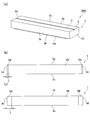
- (A) is a perspective view schematically showing an optical component 20 of a comparative example, (b) is a top view of the optical component 20, and (c) is a bottom view of the optical component 20.
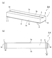
- (A) is a perspective view which shows typically the optical component 20A of a comparative example, (b), (c) is a bottom view of 20 A of optical components, respectively.
- (A) is a perspective view which shows typically 21 A of optical components of the example of this invention, (b) is a bottom view of 21 A of optical components.
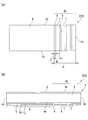
- (A) is an enlarged view of the bottom surface of the optical component 21A, and (b) is a side view showing an end portion of the optical component 21A.
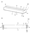
- (A) is a perspective view which shows typically the optical component 21B of the example of this invention
- (b) is a bottom view of the optical component 21B.
- (A) is an enlarged view of the end of the bottom surface of the optical component 21B
- (b) is a side view showing the end of the optical component 21B
- (c) is a view of the optical component 21B from the end surface 3d. It is a figure.
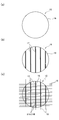
- (A) is a top view which shows the wafer 15 provided with the metal film 16, (b) shows the state which formed the non-coating part 17 on the wafer 15, (c) is the cutting
- the channel type optical waveguide 2 is formed in the element body 3.
- the element body 3 has a pair of main surfaces 3a and 3b, a pair of side surfaces 3c, and a pair of end surfaces 3d.
- the optical waveguide 2 extends between the pair of end surfaces 3d.
- this optical component In order to metal-bond this optical component to a separate substrate, it is necessary to form either one of the main surfaces 3a or 3b as a bonding surface and form a bonding metal film on the bonding surface.
- a predetermined electrode is formed on the main surface 3a, and the metal film 4 is provided on the bottom surface 3b on the opposite side.
- the metal film 4 is provided over the entire bottom surface 3b.
- the end face 3d of the optical element 20 is optically polished, if the end face is rubbed with a polishing pad, the Au metal film may be particularly finely crushed and the metal film may be peeled off and floated. . The frequency of such metal film peeling reached about 20% of the total number.
- the present inventor retreats the metal film 4A for bonding from the end surface 3d and uncovers the metal film between the edge and the end surface of the metal film. It was considered to provide 5A. That is, in the optical element 20A of this example, a predetermined electrode is formed on the main surface 3a, and the metal film 4A is provided on the bottom surface 3c on the opposite side. However, the metal film 4A is not provided over the entire bottom surface 3b. That is, the non-covering part 5A in which the metal film 4A is not provided is provided at the end part on the side of each end face 3d in the bottom face 3b. As a result, it should have been possible to prevent the metal film from peeling or floating when the end face 3d is polished.
- the optical element is very small, and it is necessary to cut out a large number of optical elements from a single wafer.
- a metal film 16 for bonding is provided on the wafer 15.
- a part of the metal film 16 is removed by etching to form a pattern 17 of an uncovered portion (see FIG. 7B).
- the wafer 15 is cut vertically and horizontally along the cutting lines 18 and 19 to obtain respective optical elements.
- the non-covered portion 5B remains in front of the end face 3d even if a positional shift occurs during cutting. We also considered making it. However, in this case, it is necessary to increase the width t of the non-covered portion 5B, so that the stability of the bonding is lowered, and heat radiation from the optical element to the substrate is reduced in the unbonded region. If the width of the non-covering part 5B becomes large and there is a misalignment at the time of cutting, the width of the non-covering part 5B tends to become remarkably large. This causes variations in characteristics.
- 3 and 4 show an optical component 21A according to an example of the present invention.
- the channel type optical waveguide 2 is formed in the element body 3.
- the element body 3 has a pair of main surfaces 3a and 3b, a pair of side surfaces 3c, and a pair of end surfaces 3d.
- the optical waveguide 2 extends between the pair of end surfaces 3d.
- a predetermined electrode is formed on the main surface 3a, the bottom surface 3b on the opposite side is used as a bonding surface, and a metal film is provided on the bottom surface.
- the main cover portion 6 was formed in a region other than the end portion 30 on the end surface 3 d side of the bottom surface 3 b.
- a plurality of rows of strip-shaped end covering portions 7 are arranged from the main covering portion 6 toward the end surface 3d.
- a slit-like non-covering portion 8 is formed between adjacent end-covering portions 7, and a slit-like non-covering portion is also provided between the innermost end-covering portion 7 and the main covering portion 6. 8 is formed.
- the end cover is provided by providing the coating portion 7 of the metal film on the end portion 30 of the joint surface 3b and providing the non-covering portion 8 between the end covering portion 7 and the main covering portion 6. Even if peeling or floating occurs due to the portion 7 rolling during optical polishing, it can be prevented from propagating to the main covering portion 6.
- the coating portion 7 made of a metal film also in the end portion 30 it is possible to ensure metal bonding between the optical component 1 and the separate substrate even in the end portion. Therefore, even if the metal film is misaligned for each optical component 1, one or more of the plurality of slits 8 are interposed between the covering portion 7 and the main covering portion 6. The progress of peeling can be prevented.
- the channel type optical waveguide 2 is formed in the element body 3.
- the element body 3 has a pair of main surfaces 3a and 3b, a pair of side surfaces 3c, and a pair of end surfaces 3d.
- the optical waveguide 2 extends between the pair of end surfaces 3d.
- a predetermined electrode is formed on the main surface 3a, the bottom surface 3b on the opposite side is used as a bonding surface, and a metal film is provided on the bottom surface.
- the main cover portion 6 was formed in a region other than the end portion 30 on the end surface 3 d side of the bottom surface 3 b.
- a plurality of quadrangular end covering portions 7A are arranged from the main covering portion 6 toward the end surface 3d, and a plurality of ends are covered between the pair of side surfaces 3c. It is arranged in a column.
- a slit-shaped non-covering portion 8A is formed between the end covering portions 7A adjacent to each other in the longitudinal direction of the bottom surface, and between the innermost end covering portion 7 and the main covering portion 6. Also, a slit-shaped uncovered portion 8A is formed. A slit-shaped non-covering portion 8B is formed between the end covering portions 7A adjacent to each other in the width direction of the bottom surface.
- the end coating is provided by providing the coating portion 7A of the metal film on the end 30 of the joint surface 3b and providing the non-covering portion 8A between the end coating 7A and the main coating 6. Even if peeling or floating occurs due to the portion 7 rolling during optical polishing, it can be prevented from propagating to the main covering portion 6.
- the coating portion 7A made of a metal film also in the end portion it is possible to ensure metal bonding between the optical component 1 and the separate substrate also in the end portion. Therefore, even if the metal film is misaligned for each optical component 1, one or more of the plurality of slits 8A are interposed between the covering portion 7 and the main covering portion 6 at the end on the end face side. The progress of peeling of the main coating portion can be reliably prevented. Furthermore, the propagation of peeling in the width direction of the bottom surface can also be suppressed by the slit-shaped uncovered portion 8B.
- the type of the optical element is not particularly limited, and may be any optical function. Specific examples include a wavelength conversion element, a light intensity modulator, an optical phase modulator, and an optical switching element.
- the type of the optical waveguide formed in the optical element is not limited, and includes a slab waveguide and a channel waveguide.
- the type of the waveguide may be an inner diffusion type optical waveguide such as a titanium diffusion method or a ridge type optical waveguide.
- a periodically poled structure is formed at least in the optical waveguide of the optical element.
- the present invention is particularly suitable for a wavelength conversion element.
- the wavelength conversion element may have a temperature deviation with respect to the waveguide direction due to heat generated by absorption of light generated by wavelength conversion.
- a temperature deviation occurs, due to the temperature dependence of the refractive index of the material, the periodic structure for performing wavelength conversion becomes effectively non-uniform in the longitudinal direction, thereby reducing the wavelength conversion efficiency.
- the optical element has a bonding surface and an optically polished end surface.
- the optical element is plate-shaped and has a pair of opposing main surfaces.
- the main surface is a surface having a relatively larger area than other surfaces. In this case, one main surface functions as a bonding surface.
- the optical element has a pair of side surfaces facing each other. In this case, in a preferred embodiment, the side surfaces are not optically polished.
- one of the pair of main surfaces is used as a bonding surface for metal bonding.
- the bottom surface 3b is used as the bonding surface.
- the surface 3a can be used as the bonding surface.
- the side surface is formed by a cutting process such as dicing, and precise optical polishing like the end surface is not performed.
- chipping of about 10 ⁇ m locally occurs by dicing.
- the metal film was not curled, peeled off or floated.
- the present invention solves the unknown problem of curling, floating, and peeling of a bonding metal film starting from an end surface on which optical polishing is performed.
- the optical element may be formed on the integrated substrate 3.
- the internal structure of the optical element is not particularly limited.
- the optical element may include a support substrate, an optical substrate made of a ferroelectric material, and an adhesive layer that bonds the support substrate and the optical substrate.
- the optical component of the present invention includes a metal film for bonding the optical element to the substrate.
- the metal film for bonding referred to here is the metal film on the outermost surface in contact with the metal for bonding, and does not include a base film or an intermediate film under the metal film for bonding.
- the base film 9, the intermediate film 10, and the bonding metal film 11 are sequentially formed on the bottom surface 3b of the optical element.
- the base film 9 and the intermediate film 10 may be provided to firmly bond the bonding metal film 11 to the optical element 1.
- the main covering portion 6 and the end covering portions 7 and 7A each mean a portion covered with the metal film 11.
- the base film 9 is exposed in the uncovered portions 8, 8A, 8B.
- the intermediate film 10 may be exposed on the non-covering portions 8, 8A, 8B.
- the optical material constituting the optical element is not particularly limited, but lithium niobate, lithium tantalate, lithium niobate-lithium tantalate solid solution, potassium lithium niobate, KTP, GaAs, and quartz, K 3 Li 2 Nb 5 O 15 La 3 Ga 5 SiO 14 and the like can be exemplified.
- one or more metal elements selected from the group consisting of magnesium (Mg), zinc (Zn), scandium (Sc), and indium (In) are used to further improve the optical damage resistance of the optical waveguide.
- Mg magnesium
- Zn zinc
- Sc scandium
- In indium
- the ferroelectric single crystal can contain a rare earth element as a doping component. This rare earth element acts as an additive element for laser oscillation. As this rare earth element, Nd, Er, Tm, Ho, Dy, and Pr are particularly preferable.
- the material of the metal film for bonding can be exemplified by gold, nickel, copper, etc. Gold is preferable for stable bonding. Since the surface of copper, nickel, or the like is easily oxidized, it may be difficult to join. Assuming that gold is formed on the surface, the base film is preferably made of chromium, titanium, or copper. When an intermediate film is used, the material is preferably nickel or platinum.
- the metal bonding method can be exemplified by direct bonding between metals in addition to solder.
- the bonding metal film includes a main covering portion that covers a region other than the end portion on the end surface side of the bonding surface, and an end covering portion that covers the bonding surface within the end portion.
- An uncoated portion that is not covered with a metal film is provided.
- At least one end covering portion is necessary, and a plurality of end covering portions are preferably present.
- at least one uncovered portion is necessary, but a plurality of non-covered portions are preferably present. This makes it easier to absorb adverse effects due to misalignment and deviation during processing.
- the uncovered portion is slit-shaped.
- the widths d, dA, and dB of the non-covered portion are preferably 1 ⁇ m or more, and more preferably 3 ⁇ m or more. Further, from the viewpoint of stability of metal bonding and heat dissipation, the widths d, dA, and dB of the non-covered portion are preferably 10 ⁇ m or less, and more preferably 5 ⁇ m or less.
- the uncovered portion extends from one side surface of the optical element toward the other side surface.
- 3 to 6 relate to this embodiment. Thereby, propagation of peeling from the end face to the main covering portion is more effectively prevented.
- the non-covering portion extends from the main covering portion toward the end surface. 5 and 6 relate to this embodiment. This further prevents propagation in the direction of the side surface of the peeling, which is more preferable.
- a plurality of end cover portions are formed at the end portions, and each end cover portion is surrounded by a non-cover portion. 5 and 6 relate to this embodiment. By thus enclosing the end covering portion with the non-covering portion, it is possible to ensure the joining at the end portion more reliably.
- each end covering portion is a stripe shape in the examples of FIGS. 3 and 4 and a square shape in the examples of FIGS.
- the planar shape of each end covering portion is not limited to a stripe shape or a quadrangle, and may be a polygon such as a triangle or a hexagon, or a circle such as a true circle or an ellipse.
- the width W of each end covering portion is preferably 3 ⁇ m or more, and more preferably 5 ⁇ m or more, from the viewpoint of ensuring metal bonding of the optical element. Further, the width W of each end covering portion is preferably 20 ⁇ m or less, and more preferably 10 ⁇ m or less, from the viewpoint of securing the space of the non-covering portion.
- the distance R from the end face 3d to the main covering portion 6 is preferably 50 ⁇ m or more, and more preferably 100 ⁇ m or more, from the viewpoint of compensating for the positional deviation of the non-covering portion due to dimensional accuracy.
- the interval R is preferably 200 ⁇ m or less, and more preferably 150 ⁇ m or less, from the viewpoint of stabilizing the metal bonding strength and promoting exhaust heat from the optical element to the substrate.
- lapping edge polishing is performed step by step while reducing the size of diamond abrasive grains, and CMP (Chemical mechanical polishing) polishing is performed using colloidal silica abrasive grains at the final finish.
- CMP Chemical mechanical polishing
- FIG. 1 An optical component having a form as shown in FIG. 1 was produced.
- the optical element 1 was formed of lithium niobate, a periodic polarization inversion structure was formed in the optical element 1, and a ridge-type channel optical waveguide 2 was formed.
- a comb-like periodic electrode having a period of 6.6 ⁇ m was formed by photolithography on a 5-degree off-y-cut MgO 5% doped lithium niobate substrate having a thickness of 0.5 mm.
- a uniform electrode was formed on the entire back surface of the substrate, and then a pulse voltage was applied to form a periodically poled structure.
- a 0.6 um thick SiO 2 underclad was formed by sputtering.
- An adhesive was applied to a 0.5 mm thick lithium niobate substrate, and then bonded to the MgO-doped lithium niobate substrate.
- the surface of the MgO-doped lithium niobate substrate was ground and polished to a thickness of 3.7 ⁇ m.
- a 0.6 ⁇ m thick SiO 2 overclad was formed by sputtering.
- a chromium film having a thickness of 500 angstroms, a nickel film having a thickness of 2,000 angstroms, and a gold film having a thickness of 500 angstroms were formed on the entire bottom surface 3b of the obtained optical element 1 by sputtering.
- the gold film is a bonding metal film
- the chromium film is a base film
- the nickel film is an intermediate film.
- a chromium film, a nickel film, and a gold film were formed over the entire bottom surface 3b of the optical element 1.
- the obtained wafer was cut with a dicer as shown in 18 of FIG. 7C to obtain a long and narrow cut (dimension of about 10 mm ⁇ about 30 mm: if long, cut into two or three parts. Was aligned to 30 mm).
- This cut product was fixed to an end surface polishing jig and subjected to end surface polishing with diamond abrasive grains and colloidal silica abrasive grains, and then antireflection films were applied to both end faces.
- This elongated cut product was further cut as in 19 to obtain an optical component having a width of 0.8 mm.
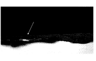
- FIG. 8 is a photograph observed near the end face of the obtained optical component with the metal film facing forward.
- the end surface extends in the lateral direction in the center of FIG. 8, and the black portion above the end surface is a space.
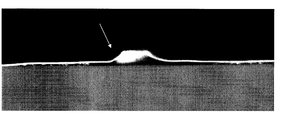
- FIG. 9 is a photograph of the obtained optical component cut and the end face observed. Protrusions can be seen in the area indicated by the arrow, but this indicates that the chromium film, which is the underlying film, has been rolled up by optical polishing. This represents a phenomenon in which nickel and even the underlying chromium are peeled off.
- Comparative Example 2 An optical component was produced in the same manner as in Comparative Example 1. However, in this example, as shown in FIG. 2B, the non-covering portion 5A was formed at the end portion on the end face side of the bottom surface to expose the chromium film.
- the width t of the non-covered portion needs to be 50 ⁇ m or more in order to leave the non-covered portion at the end and polish the end surface with a high yield.
- the end surface polishing may process a narrow or wide portion of the Cr region, and in particular, an uncovered portion having a very large width may be formed.
- the width of the uncovered portion is large, the region that is not joined becomes large, and the heat exhausting property to the substrate is deteriorated. The length of this region does not contribute to wavelength conversion at all, and the wavelength conversion efficiency is lowered.
- Example 1 An optical component was produced in the same manner as in Comparative Example 1. However, in this example, as shown in FIG. 3 and FIG. 4, the non-covering portion 8 and the end covering portion 7 were formed at the end portion on the end face side of the bottom surface to expose the chromium film. The number of uncovered portions 8 was 21, and the width was 2 ⁇ m. Further, the number of end covering portions was 20, and the width was 6 ⁇ m.
- Such a metal film pattern can be easily and collectively patterned for a plurality of optical components by patterning on a wafer, as shown at 17 in FIG. 7B.
- FIG. 10 is a photograph of the end surface where peeling occurred
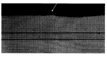
- FIG. 11 shows the end surface where the metal film was not peeled and polished.
- the gold film was peeled off so as to bend from the end face.
- An arrow shows a peeling part.
- the edge part is divided into three parts, the uppermost part is the edge cover part 7, the non-cover part 8 is below it, and the edge cover part 7 is below it. This is because, when the end face is polished, soft Au is avoided on the polishing pad, and Au is drowned. Furthermore, at the point where Au burned, the underlying nickel film and chromium film were also stuck and drowned.
- FIG. 11 the photograph of the state without peeling in the vicinity of an end surface is shown.
- Example 2 An optical component was produced in the same manner as in Comparative Example 1. However, in this example, as shown in FIGS. 5 and 6, the non-covering portions 8A and 8B and the end covering portion 7A were formed at the end portion on the end face side of the bottom surface to expose the chromium film. The uncovered portions 8A and 8B were 21 and 101, respectively, and the width was 2 ⁇ m. Further, the end covering portion 7A was 20 ⁇ 100 rows, and each dimension was 6 ⁇ m ⁇ 6 ⁇ m.
Landscapes
- Physics & Mathematics (AREA)
- Nonlinear Science (AREA)
- General Physics & Mathematics (AREA)
- Optics & Photonics (AREA)
- Chemical & Material Sciences (AREA)
- Crystallography & Structural Chemistry (AREA)
- Engineering & Computer Science (AREA)
- Microelectronics & Electronic Packaging (AREA)
- Optical Integrated Circuits (AREA)
- Optical Modulation, Optical Deflection, Nonlinear Optics, Optical Demodulation, Optical Logic Elements (AREA)
Abstract
Description
光学素子の接合面に形成された、光学素子を基板に対して接合するための金属膜を備えており、金属膜が、接合面の端面側の端部以外の領域を被覆する主被覆部と、接合面を前記端部内で被覆する端部被覆部とを含んでおり、金属膜が被覆されていない非被覆部が端部に設けられていることを特徴とする。
光学素子の種類は特に限定されず、光学的機能を果たせばよい。具体的には、波長変換素子、光強度変調器、光位相変調器、光スイッチング素子などを例示できる。
ダイシングによりウェハーから素子を切断後、ダイヤモンド砥粒の大きさを小さくしつつ段階を踏んでラッピング端面研磨を行い、最後の仕上げで、コロイダルシリカ砥粒を使用してCMP(Chemical mechanical polishing)研磨を行う。
図1に示すような形態の光学部品を作製した。
ただし、光学素子1をニオブ酸リチウムによって形成し、光学素子1内に周期分極反転構造を形成するとともに、リッジ型のチャンネル光導波路2を形成した。
比較例1と同様にして光学部品を作製した。ただし、本例では、図2(b)に示すように、底面の端面側の端部に非被覆部5Aを形成し、クロム膜を露出させた。
比較例1と同様にして光学部品を作製した。ただし、本例では、図3、図4に示すように、底面の端面側の端部に非被覆部8および端部被覆部7を形成し、クロム膜を露出させた。非被覆部8は21本とし、幅は2μmとした。また端部被覆部は20本とし、幅は6μmとした。
図10は、端面で剥がれが生じたものの写真であり、図11は、端面で金属膜の剥がれがなく研磨できたものである。
なお、図11には、端面付近で剥離がない状態の写真を示す。
比較例1と同様にして光学部品を作製した。ただし、本例では、図5、図6に示すように、底面の端面側の端部に非被覆部8A、8Bおよび端部被覆部7Aを形成し、クロム膜を露出させた。非被覆部8A、8Bはそれぞれ21本、101本とし、幅は2μmとした。また端部被覆部7Aは20×100列とし、それぞれ寸法は6μm×6μmとした。
Claims (11)
- 接合面および光学研磨された端面を有している光学素子、および
前記光学素子の前記接合面に形成された、前記光学素子を基板に対して接合するための金属膜を備える光学部品であって、
前記金属膜が、前記接合面の前記端面側の端部以外の領域を被覆する主被覆部と、前記接合面を前記端部内で被覆する端部被覆部とを含んでおり、前記金属膜によって被覆されていない非被覆部が前記端部に設けられていることを特徴とする、光学部品。 - 前記光学素子に光導波路が形成されていることを特徴とする、請求項1記載の光学部品。
- 前記光学素子に周期分極反転構造が形成されていることを特徴とする、請求項1または2記載の光学部品。
- 前記非被覆部がスリット状であることを特徴とする、請求項1~3のいずれか一つの請求項に記載の光学部品。
- 前記非被覆部が前記主被覆部と前記端面との間に延びていることを特徴とする、請求項4記載の光学部品。
- 前記光学素子が、相対向する一対の主面および相対向する一対の側面を有しており、前記一対の主面の一方が前記接合面として機能することを特徴とする、請求項1~5のいずれか一つの請求項に記載の光学部品。
- 前記非被覆部が前記光学素子の前記一対の側面の間に延びていることを特徴とする、請求項6記載の光学部品。
- 前記端部において複数の前記端部被覆部が形成されており、各端部被覆部が前記非被覆部によって包囲されていることを特徴とする、請求項1~7のいずれか一つの請求項に記載の光学部品。
- 前記金属膜が金膜であることを特徴とする、請求項1~8のいずれか一つの請求項に記載の光学部品。
- 前記金属膜と前記接合面との間に形成された下地膜を有しており、前記下地膜が前記非被覆部に露出していることを特徴とする、請求項1~9のいずれか一つの請求項に記載の光学部品。
- 前記光学素子が、
支持基板、
光学材料からなる光学基板、および
前記支持基板と前記光学基板とを接着する接着層を備えていることを特徴とする、請求項1~10のいずれか一つの請求項に記載の光学部品。
Priority Applications (4)
| Application Number | Priority Date | Filing Date | Title |
|---|---|---|---|
| CN201480050094.1A CN105556354B (zh) | 2013-09-30 | 2014-08-15 | 光学部件 |
| JP2015539015A JP6144770B2 (ja) | 2013-09-30 | 2014-08-15 | 光学部品 |
| DE112014004499.7T DE112014004499B4 (de) | 2013-09-30 | 2014-08-15 | Optisches Bauteil |
| US15/078,088 US9733546B2 (en) | 2013-09-30 | 2016-03-23 | Optical component |
Applications Claiming Priority (2)
| Application Number | Priority Date | Filing Date | Title |
|---|---|---|---|
| JP2013204584 | 2013-09-30 | ||
| JP2013-204584 | 2013-09-30 |
Related Child Applications (1)
| Application Number | Title | Priority Date | Filing Date |
|---|---|---|---|
| US15/078,088 Continuation US9733546B2 (en) | 2013-09-30 | 2016-03-23 | Optical component |
Publications (1)
| Publication Number | Publication Date |
|---|---|
| WO2015045668A1 true WO2015045668A1 (ja) | 2015-04-02 |
Family
ID=52742822
Family Applications (1)
| Application Number | Title | Priority Date | Filing Date |
|---|---|---|---|
| PCT/JP2014/071479 Ceased WO2015045668A1 (ja) | 2013-09-30 | 2014-08-15 | 光学部品 |
Country Status (5)
| Country | Link |
|---|---|
| US (1) | US9733546B2 (ja) |
| JP (1) | JP6144770B2 (ja) |
| CN (1) | CN105556354B (ja) |
| DE (1) | DE112014004499B4 (ja) |
| WO (1) | WO2015045668A1 (ja) |
Citations (3)
| Publication number | Priority date | Publication date | Assignee | Title |
|---|---|---|---|---|
| JP2003270467A (ja) * | 2002-01-09 | 2003-09-25 | Matsushita Electric Ind Co Ltd | 光導波路デバイスの製造方法、光導波路デバイス並びに当該光導波路デバイスを用いたコヒーレント光源及び光学装置 |
| JP2003295140A (ja) * | 2002-03-29 | 2003-10-15 | Japan Science & Technology Corp | 光周波数コム発生器及びその製造方法 |
| JP2010204505A (ja) * | 2009-03-05 | 2010-09-16 | Ngk Insulators Ltd | 波長変換素子およびその製造方法 |
Family Cites Families (7)
| Publication number | Priority date | Publication date | Assignee | Title |
|---|---|---|---|---|
| US5834829A (en) * | 1996-09-05 | 1998-11-10 | International Business Machines Corporation | Energy relieving crack stop |
| US6999668B2 (en) | 2002-01-09 | 2006-02-14 | Matsushita Electric Industrial Co., Ltd. | Method for manufacturing optical waveguide device, optical waveguide device, and coherent light source and optical apparatus using the optical waveguide device |
| CN1936629A (zh) * | 2002-05-31 | 2007-03-28 | 松下电器产业株式会社 | 光学元件的制造方法 |
| US6833323B2 (en) * | 2003-01-29 | 2004-12-21 | Taiwan Semiconductor Manufacturing Co., Ltd | Method for forming patterned features at a semiconductor wafer periphery to prevent metal peeling |
| JP4302505B2 (ja) * | 2003-12-22 | 2009-07-29 | Okiセミコンダクタ株式会社 | 半導体装置 |
| JP2007317736A (ja) * | 2006-05-23 | 2007-12-06 | Toshiba Corp | 半導体装置およびその製造方法 |
| US8809109B2 (en) * | 2012-05-21 | 2014-08-19 | Stion Corporation | Method and structure for eliminating edge peeling in thin-film photovoltaic absorber materials |
-
2014
- 2014-08-15 JP JP2015539015A patent/JP6144770B2/ja active Active
- 2014-08-15 CN CN201480050094.1A patent/CN105556354B/zh active Active
- 2014-08-15 WO PCT/JP2014/071479 patent/WO2015045668A1/ja not_active Ceased
- 2014-08-15 DE DE112014004499.7T patent/DE112014004499B4/de active Active
-
2016
- 2016-03-23 US US15/078,088 patent/US9733546B2/en active Active
Patent Citations (3)
| Publication number | Priority date | Publication date | Assignee | Title |
|---|---|---|---|---|
| JP2003270467A (ja) * | 2002-01-09 | 2003-09-25 | Matsushita Electric Ind Co Ltd | 光導波路デバイスの製造方法、光導波路デバイス並びに当該光導波路デバイスを用いたコヒーレント光源及び光学装置 |
| JP2003295140A (ja) * | 2002-03-29 | 2003-10-15 | Japan Science & Technology Corp | 光周波数コム発生器及びその製造方法 |
| JP2010204505A (ja) * | 2009-03-05 | 2010-09-16 | Ngk Insulators Ltd | 波長変換素子およびその製造方法 |
Also Published As
| Publication number | Publication date |
|---|---|
| US9733546B2 (en) | 2017-08-15 |
| CN105556354A (zh) | 2016-05-04 |
| JP6144770B2 (ja) | 2017-06-07 |
| JPWO2015045668A1 (ja) | 2017-03-09 |
| DE112014004499B4 (de) | 2024-03-28 |
| US20160202596A1 (en) | 2016-07-14 |
| CN105556354B (zh) | 2018-12-21 |
| DE112014004499T5 (de) | 2016-06-16 |
Similar Documents
| Publication | Publication Date | Title |
|---|---|---|
| JP7075448B2 (ja) | 電気光学素子のための複合基板 | |
| JP5951589B2 (ja) | 光導波路素子 | |
| JP5164192B2 (ja) | 光導波路基板および高調波発生デバイス | |
| US7382942B2 (en) | Optical waveguide devices | |
| US9298025B2 (en) | Electrode structure for an optical waveguide substrate | |
| JP7295467B2 (ja) | 光学素子及びその製造方法 | |
| CN102841481A (zh) | 光学器件以及光学器件的制造方法 | |
| CN101535888B (zh) | 光波导基板的制造方法 | |
| JP6144770B2 (ja) | 光学部品 | |
| JP4806427B2 (ja) | 波長変換素子およびその製造方法 | |
| WO2014030404A1 (ja) | 波長変換素子 | |
| JP4806424B2 (ja) | 高調波発生素子 | |
| JP7204103B2 (ja) | テラヘルツ波発生素子及びその製造方法 | |
| US10082683B2 (en) | Optical modulator that is formed using ferroelectric substrate | |
| JP5494400B2 (ja) | 光導波路素子 | |
| JP2008102228A (ja) | 光学素子および光学素子の製造方法 | |
| JP2010039317A (ja) | 光学素子および光学素子の製造方法 | |
| JP3885939B2 (ja) | 光導波路デバイスの製造方法 | |
| JP2016024423A (ja) | 波長変換素子の製造方法および波長変換素子 | |
| US20250328036A1 (en) | Optical Modulator and Optical Transmission Device Using Same | |
| WO2011024781A1 (ja) | 波長変換素子及びその製造方法 | |
| WO2024201864A1 (ja) | 光導波路素子とそれを用いた光変調デバイス並びに光送信装置 | |
| JP5428132B2 (ja) | 光学素子の製造方法および光学素子 | |
| JP5556787B2 (ja) | 光制御素子の製造方法 | |
| JP2007079465A (ja) | 光制御素子及びその製造方法 |
Legal Events
| Date | Code | Title | Description |
|---|---|---|---|
| WWE | Wipo information: entry into national phase |
Ref document number: 201480050094.1 Country of ref document: CN |
|
| 121 | Ep: the epo has been informed by wipo that ep was designated in this application |
Ref document number: 14847302 Country of ref document: EP Kind code of ref document: A1 |
|
| ENP | Entry into the national phase |
Ref document number: 2015539015 Country of ref document: JP Kind code of ref document: A |
|
| WWE | Wipo information: entry into national phase |
Ref document number: 1120140044997 Country of ref document: DE Ref document number: 112014004499 Country of ref document: DE |
|
| 122 | Ep: pct application non-entry in european phase |
Ref document number: 14847302 Country of ref document: EP Kind code of ref document: A1 |