WO2015045653A1 - 炭化珪素半導体装置の製造方法 - Google Patents
炭化珪素半導体装置の製造方法 Download PDFInfo
- Publication number
- WO2015045653A1 WO2015045653A1 PCT/JP2014/071165 JP2014071165W WO2015045653A1 WO 2015045653 A1 WO2015045653 A1 WO 2015045653A1 JP 2014071165 W JP2014071165 W JP 2014071165W WO 2015045653 A1 WO2015045653 A1 WO 2015045653A1
- Authority
- WO
- WIPO (PCT)
- Prior art keywords
- silicon carbide
- layer
- carbon layer
- semiconductor device
- manufacturing
- Prior art date
- Legal status (The legal status is an assumption and is not a legal conclusion. Google has not performed a legal analysis and makes no representation as to the accuracy of the status listed.)
- Ceased
Links
Images




Classifications
-
- H—ELECTRICITY
- H10—SEMICONDUCTOR DEVICES; ELECTRIC SOLID-STATE DEVICES NOT OTHERWISE PROVIDED FOR
- H10D—INORGANIC ELECTRIC SEMICONDUCTOR DEVICES
- H10D62/00—Semiconductor bodies, or regions thereof, of devices having potential barriers
- H10D62/80—Semiconductor bodies, or regions thereof, of devices having potential barriers characterised by the materials
- H10D62/83—Semiconductor bodies, or regions thereof, of devices having potential barriers characterised by the materials being Group IV materials, e.g. B-doped Si or undoped Ge
- H10D62/832—Semiconductor bodies, or regions thereof, of devices having potential barriers characterised by the materials being Group IV materials, e.g. B-doped Si or undoped Ge being Group IV materials comprising two or more elements, e.g. SiGe
- H10D62/8325—Silicon carbide
-
- H—ELECTRICITY
- H10—SEMICONDUCTOR DEVICES; ELECTRIC SOLID-STATE DEVICES NOT OTHERWISE PROVIDED FOR
- H10D—INORGANIC ELECTRIC SEMICONDUCTOR DEVICES
- H10D62/00—Semiconductor bodies, or regions thereof, of devices having potential barriers
- H10D62/40—Crystalline structures
- H10D62/405—Orientations of crystalline planes
-
- H—ELECTRICITY
- H10—SEMICONDUCTOR DEVICES; ELECTRIC SOLID-STATE DEVICES NOT OTHERWISE PROVIDED FOR
- H10D—INORGANIC ELECTRIC SEMICONDUCTOR DEVICES
- H10D12/00—Bipolar devices controlled by the field effect, e.g. insulated-gate bipolar transistors [IGBT]
- H10D12/01—Manufacture or treatment
- H10D12/031—Manufacture or treatment of IGBTs
-
- H—ELECTRICITY
- H10—SEMICONDUCTOR DEVICES; ELECTRIC SOLID-STATE DEVICES NOT OTHERWISE PROVIDED FOR
- H10D—INORGANIC ELECTRIC SEMICONDUCTOR DEVICES
- H10D30/00—Field-effect transistors [FET]
- H10D30/01—Manufacture or treatment
- H10D30/021—Manufacture or treatment of FETs having insulated gates [IGFET]
- H10D30/028—Manufacture or treatment of FETs having insulated gates [IGFET] of double-diffused metal oxide semiconductor [DMOS] FETs
- H10D30/0291—Manufacture or treatment of FETs having insulated gates [IGFET] of double-diffused metal oxide semiconductor [DMOS] FETs of vertical DMOS [VDMOS] FETs
- H10D30/0297—Manufacture or treatment of FETs having insulated gates [IGFET] of double-diffused metal oxide semiconductor [DMOS] FETs of vertical DMOS [VDMOS] FETs using recessing of the gate electrodes, e.g. to form trench gate electrodes
-
- H—ELECTRICITY
- H10—SEMICONDUCTOR DEVICES; ELECTRIC SOLID-STATE DEVICES NOT OTHERWISE PROVIDED FOR
- H10D—INORGANIC ELECTRIC SEMICONDUCTOR DEVICES
- H10D30/00—Field-effect transistors [FET]
- H10D30/60—Insulated-gate field-effect transistors [IGFET]
- H10D30/64—Double-diffused metal-oxide semiconductor [DMOS] FETs
- H10D30/66—Vertical DMOS [VDMOS] FETs
- H10D30/665—Vertical DMOS [VDMOS] FETs having edge termination structures
-
- H—ELECTRICITY
- H10—SEMICONDUCTOR DEVICES; ELECTRIC SOLID-STATE DEVICES NOT OTHERWISE PROVIDED FOR
- H10D—INORGANIC ELECTRIC SEMICONDUCTOR DEVICES
- H10D30/00—Field-effect transistors [FET]
- H10D30/60—Insulated-gate field-effect transistors [IGFET]
- H10D30/64—Double-diffused metal-oxide semiconductor [DMOS] FETs
- H10D30/66—Vertical DMOS [VDMOS] FETs
- H10D30/668—Vertical DMOS [VDMOS] FETs having trench gate electrodes, e.g. UMOS transistors
-
- H—ELECTRICITY
- H10—SEMICONDUCTOR DEVICES; ELECTRIC SOLID-STATE DEVICES NOT OTHERWISE PROVIDED FOR
- H10D—INORGANIC ELECTRIC SEMICONDUCTOR DEVICES
- H10D62/00—Semiconductor bodies, or regions thereof, of devices having potential barriers
- H10D62/10—Shapes, relative sizes or dispositions of the regions of the semiconductor bodies; Shapes of the semiconductor bodies
- H10D62/102—Constructional design considerations for preventing surface leakage or controlling electric field concentration
- H10D62/103—Constructional design considerations for preventing surface leakage or controlling electric field concentration for increasing or controlling the breakdown voltage of reverse-biased devices
- H10D62/104—Constructional design considerations for preventing surface leakage or controlling electric field concentration for increasing or controlling the breakdown voltage of reverse-biased devices having particular shapes of the bodies at or near reverse-biased junctions, e.g. having bevels or moats
-
- H—ELECTRICITY
- H10—SEMICONDUCTOR DEVICES; ELECTRIC SOLID-STATE DEVICES NOT OTHERWISE PROVIDED FOR
- H10D—INORGANIC ELECTRIC SEMICONDUCTOR DEVICES
- H10D62/00—Semiconductor bodies, or regions thereof, of devices having potential barriers
- H10D62/10—Shapes, relative sizes or dispositions of the regions of the semiconductor bodies; Shapes of the semiconductor bodies
- H10D62/102—Constructional design considerations for preventing surface leakage or controlling electric field concentration
- H10D62/103—Constructional design considerations for preventing surface leakage or controlling electric field concentration for increasing or controlling the breakdown voltage of reverse-biased devices
- H10D62/105—Constructional design considerations for preventing surface leakage or controlling electric field concentration for increasing or controlling the breakdown voltage of reverse-biased devices by having particular doping profiles, shapes or arrangements of PN junctions; by having supplementary regions, e.g. junction termination extension [JTE]
-
- H—ELECTRICITY
- H10—SEMICONDUCTOR DEVICES; ELECTRIC SOLID-STATE DEVICES NOT OTHERWISE PROVIDED FOR
- H10D—INORGANIC ELECTRIC SEMICONDUCTOR DEVICES
- H10D62/00—Semiconductor bodies, or regions thereof, of devices having potential barriers
- H10D62/10—Shapes, relative sizes or dispositions of the regions of the semiconductor bodies; Shapes of the semiconductor bodies
- H10D62/102—Constructional design considerations for preventing surface leakage or controlling electric field concentration
- H10D62/103—Constructional design considerations for preventing surface leakage or controlling electric field concentration for increasing or controlling the breakdown voltage of reverse-biased devices
- H10D62/105—Constructional design considerations for preventing surface leakage or controlling electric field concentration for increasing or controlling the breakdown voltage of reverse-biased devices by having particular doping profiles, shapes or arrangements of PN junctions; by having supplementary regions, e.g. junction termination extension [JTE]
- H10D62/106—Constructional design considerations for preventing surface leakage or controlling electric field concentration for increasing or controlling the breakdown voltage of reverse-biased devices by having particular doping profiles, shapes or arrangements of PN junctions; by having supplementary regions, e.g. junction termination extension [JTE] having supplementary regions doped oppositely to or in rectifying contact with regions of the semiconductor bodies, e.g. guard rings with PN or Schottky junctions
-
- H—ELECTRICITY
- H10—SEMICONDUCTOR DEVICES; ELECTRIC SOLID-STATE DEVICES NOT OTHERWISE PROVIDED FOR
- H10D—INORGANIC ELECTRIC SEMICONDUCTOR DEVICES
- H10D62/00—Semiconductor bodies, or regions thereof, of devices having potential barriers
- H10D62/10—Shapes, relative sizes or dispositions of the regions of the semiconductor bodies; Shapes of the semiconductor bodies
- H10D62/17—Semiconductor regions connected to electrodes not carrying current to be rectified, amplified or switched, e.g. channel regions
- H10D62/393—Body regions of DMOS transistors or IGBTs
-
- H—ELECTRICITY
- H10—SEMICONDUCTOR DEVICES; ELECTRIC SOLID-STATE DEVICES NOT OTHERWISE PROVIDED FOR
- H10D—INORGANIC ELECTRIC SEMICONDUCTOR DEVICES
- H10D62/00—Semiconductor bodies, or regions thereof, of devices having potential barriers
- H10D62/80—Semiconductor bodies, or regions thereof, of devices having potential barriers characterised by the materials
- H10D62/83—Semiconductor bodies, or regions thereof, of devices having potential barriers characterised by the materials being Group IV materials, e.g. B-doped Si or undoped Ge
- H10D62/8303—Diamond
-
- H—ELECTRICITY
- H10—SEMICONDUCTOR DEVICES; ELECTRIC SOLID-STATE DEVICES NOT OTHERWISE PROVIDED FOR
- H10D—INORGANIC ELECTRIC SEMICONDUCTOR DEVICES
- H10D64/00—Electrodes of devices having potential barriers
- H10D64/01—Manufacture or treatment
- H10D64/013—Manufacture or treatment of electrodes having a conductor capacitively coupled to a semiconductor by an insulator
- H10D64/01366—Manufacture or treatment of electrodes having a conductor capacitively coupled to a semiconductor by an insulator the semiconductor being silicon carbide
-
- H—ELECTRICITY
- H10—SEMICONDUCTOR DEVICES; ELECTRIC SOLID-STATE DEVICES NOT OTHERWISE PROVIDED FOR
- H10P—GENERIC PROCESSES OR APPARATUS FOR THE MANUFACTURE OR TREATMENT OF DEVICES COVERED BY CLASS H10
- H10P30/00—Ion implantation into wafers, substrates or parts of devices
- H10P30/20—Ion implantation into wafers, substrates or parts of devices into semiconductor materials, e.g. for doping
- H10P30/202—Ion implantation into wafers, substrates or parts of devices into semiconductor materials, e.g. for doping characterised by the semiconductor materials
- H10P30/204—Ion implantation into wafers, substrates or parts of devices into semiconductor materials, e.g. for doping characterised by the semiconductor materials into Group IV semiconductors
- H10P30/2042—Ion implantation into wafers, substrates or parts of devices into semiconductor materials, e.g. for doping characterised by the semiconductor materials into Group IV semiconductors into crystalline silicon carbide
-
- H—ELECTRICITY
- H10—SEMICONDUCTOR DEVICES; ELECTRIC SOLID-STATE DEVICES NOT OTHERWISE PROVIDED FOR
- H10P—GENERIC PROCESSES OR APPARATUS FOR THE MANUFACTURE OR TREATMENT OF DEVICES COVERED BY CLASS H10
- H10P30/00—Ion implantation into wafers, substrates or parts of devices
- H10P30/20—Ion implantation into wafers, substrates or parts of devices into semiconductor materials, e.g. for doping
- H10P30/21—Ion implantation into wafers, substrates or parts of devices into semiconductor materials, e.g. for doping of electrically active species
-
- H—ELECTRICITY
- H10—SEMICONDUCTOR DEVICES; ELECTRIC SOLID-STATE DEVICES NOT OTHERWISE PROVIDED FOR
- H10P—GENERIC PROCESSES OR APPARATUS FOR THE MANUFACTURE OR TREATMENT OF DEVICES COVERED BY CLASS H10
- H10P30/00—Ion implantation into wafers, substrates or parts of devices
- H10P30/20—Ion implantation into wafers, substrates or parts of devices into semiconductor materials, e.g. for doping
- H10P30/22—Ion implantation into wafers, substrates or parts of devices into semiconductor materials, e.g. for doping using masks
-
- H—ELECTRICITY
- H10—SEMICONDUCTOR DEVICES; ELECTRIC SOLID-STATE DEVICES NOT OTHERWISE PROVIDED FOR
- H10P—GENERIC PROCESSES OR APPARATUS FOR THE MANUFACTURE OR TREATMENT OF DEVICES COVERED BY CLASS H10
- H10P32/00—Diffusion of dopants within, into or out of wafers, substrates or parts of devices
- H10P32/10—Diffusion of dopants within, into or out of semiconductor bodies or layers
- H10P32/17—Diffusion of dopants within, into or out of semiconductor bodies or layers characterised by the semiconductor material
- H10P32/171—Diffusion of dopants within, into or out of semiconductor bodies or layers characterised by the semiconductor material being group IV material
- H10P32/172—Diffusion of dopants within, into or out of semiconductor bodies or layers characterised by the semiconductor material being group IV material being crystalline silicon carbide
-
- H—ELECTRICITY
- H10—SEMICONDUCTOR DEVICES; ELECTRIC SOLID-STATE DEVICES NOT OTHERWISE PROVIDED FOR
- H10P—GENERIC PROCESSES OR APPARATUS FOR THE MANUFACTURE OR TREATMENT OF DEVICES COVERED BY CLASS H10
- H10P50/00—Etching of wafers, substrates or parts of devices
-
- H—ELECTRICITY
- H10—SEMICONDUCTOR DEVICES; ELECTRIC SOLID-STATE DEVICES NOT OTHERWISE PROVIDED FOR
- H10P—GENERIC PROCESSES OR APPARATUS FOR THE MANUFACTURE OR TREATMENT OF DEVICES COVERED BY CLASS H10
- H10P50/00—Etching of wafers, substrates or parts of devices
- H10P50/20—Dry etching; Plasma etching; Reactive-ion etching
- H10P50/24—Dry etching; Plasma etching; Reactive-ion etching of semiconductor materials
- H10P50/242—Dry etching; Plasma etching; Reactive-ion etching of semiconductor materials of Group IV materials
-
- H—ELECTRICITY
- H10—SEMICONDUCTOR DEVICES; ELECTRIC SOLID-STATE DEVICES NOT OTHERWISE PROVIDED FOR
- H10P—GENERIC PROCESSES OR APPARATUS FOR THE MANUFACTURE OR TREATMENT OF DEVICES COVERED BY CLASS H10
- H10P95/00—Generic processes or apparatus for manufacture or treatments not covered by the other groups of this subclass
- H10P95/90—Thermal treatments, e.g. annealing or sintering
-
- H—ELECTRICITY
- H10—SEMICONDUCTOR DEVICES; ELECTRIC SOLID-STATE DEVICES NOT OTHERWISE PROVIDED FOR
- H10P—GENERIC PROCESSES OR APPARATUS FOR THE MANUFACTURE OR TREATMENT OF DEVICES COVERED BY CLASS H10
- H10P14/00—Formation of materials, e.g. in the shape of layers or pillars
- H10P14/60—Formation of materials, e.g. in the shape of layers or pillars of insulating materials
- H10P14/69—Inorganic materials
- H10P14/6902—Inorganic materials composed of carbon, e.g. alpha-C, diamond or hydrogen doped carbon
-
- H—ELECTRICITY
- H10—SEMICONDUCTOR DEVICES; ELECTRIC SOLID-STATE DEVICES NOT OTHERWISE PROVIDED FOR
- H10P—GENERIC PROCESSES OR APPARATUS FOR THE MANUFACTURE OR TREATMENT OF DEVICES COVERED BY CLASS H10
- H10P95/00—Generic processes or apparatus for manufacture or treatments not covered by the other groups of this subclass
- H10P95/08—Planarisation of organic insulating materials
Definitions
- the present invention relates to a method for manufacturing a silicon carbide semiconductor device, and more specifically, to perform activation annealing in a state in which a decrease in manufacturing efficiency is suppressed and the surface of the silicon carbide layer is more reliably protected.
- the present invention relates to a method for manufacturing a silicon carbide semiconductor device that can be used.
- silicon carbide has been increasingly adopted as a material constituting semiconductor devices in order to enable higher breakdown voltage, lower loss, and use in high-temperature environments.
- Silicon carbide is a wide band gap semiconductor having a larger band gap than silicon that has been widely used as a material for forming semiconductor devices. Therefore, by adopting silicon carbide as a material constituting the semiconductor device, it is possible to achieve a high breakdown voltage and a low on-resistance of the semiconductor device.
- a semiconductor device that employs silicon carbide as a material has an advantage that a decrease in characteristics when used in a high temperature environment is small as compared with a semiconductor device that employs silicon as a material.
- Patent Document 1 discloses a process of activation annealing in a state where a diamond-like carbon (DLC: Diamond Like Carbon) film or a film obtained by carbonizing a photoresist film is deposited on the surface of an epitaxial growth layer (silicon carbide layer).
- DLC Diamond Like Carbon
- Patent Document 2 discloses a process in which a carbon layer is formed by selectively removing silicon from a surface layer portion of a silicon carbide layer, and then activation annealing is performed.
- a carbon layer is formed on the surface of the silicon carbide layer by a method such as a CVD (Chemical Vapor Deposition) method or a sputtering method.
- the CVD method has a problem that the film coverage is deteriorated when the level difference or unevenness on the surface of the silicon carbide layer is large, and the sputtering method has a problem that the adhesion of the film is low and cracking is likely to occur.
- the variation of the film thickness in the surface becomes large (the film thickness distribution becomes worse). Therefore, with these methods, it is difficult to perform activation annealing in a state where the surface of the silicon carbide layer is sufficiently protected.
- the present invention has been made in view of the above problems, and its purpose is to perform activation annealing in a state in which a decrease in production efficiency is suppressed and the surface of the silicon carbide layer is more reliably protected. It is providing the manufacturing method of the silicon carbide semiconductor device which can do.
- a method of manufacturing a silicon carbide semiconductor device includes a step of forming an impurity region in a silicon carbide layer, and selectively removing silicon from the surface of the silicon carbide layer in which the impurity region is formed. Forming the first carbon layer, forming the second carbon layer on the first carbon layer, and heating the silicon carbide layer on which the first carbon layer and the second carbon layer are formed. I have.
- activation annealing can be performed in a state in which a decrease in manufacturing efficiency is suppressed and the surface of the silicon carbide layer is more reliably protected.
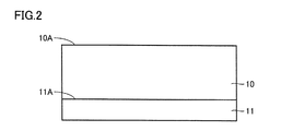
- FIG. 3 is a flowchart schematically showing a method for manufacturing the silicon carbide semiconductor device according to the first embodiment.
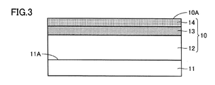
- FIG. 6 is a schematic diagram for illustrating steps (S10) and (S20) in the method for manufacturing the silicon carbide semiconductor device according to the first embodiment. It is the schematic for demonstrating the process (S30) in the manufacturing method of the silicon carbide semiconductor device which concerns on Embodiment 1.
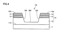
- FIG. It is the schematic for demonstrating the process (S40) in the manufacturing method of the silicon carbide semiconductor device which concerns on Embodiment 1.
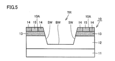
- FIG. It is the schematic for demonstrating the process (S50) in the manufacturing method of the silicon carbide semiconductor device which concerns on Embodiment 1.
- FIG. 5 is a graph showing a heating pattern in steps (S70) and (S80) of the method for manufacturing the silicon carbide semiconductor device according to the first embodiment. It is the schematic for demonstrating the process (S100) in the manufacturing method of the silicon carbide semiconductor device which concerns on Embodiment 1.
- FIG. FIG. 5 is a graph showing a heating pattern in steps (S70) and (S80) of the method for manufacturing the silicon carbide semiconductor device according to the first embodiment.
- FIG. 6 is a schematic diagram for illustrating a step (S110) in the method for manufacturing the silicon carbide semiconductor device according to the first embodiment.
- FIG. 6 is a schematic diagram for illustrating steps (S120) and (S130) in the method for manufacturing the silicon carbide semiconductor device according to the first embodiment. It is the schematic for demonstrating the process (S140) in the manufacturing method of the silicon carbide semiconductor device which concerns on Embodiment 1.
- FIG. 3 is a schematic diagram showing a structure of a termination region of a silicon carbide layer according to Embodiment 1.
- FIG. It is the schematic which shows the structure of the termination
- FIG. 10 is a schematic diagram for illustrating the method for manufacturing the silicon carbide semiconductor device according to the second embodiment.
- a method for manufacturing a silicon carbide semiconductor device includes a step of forming impurity regions (13, 14, 15) in a silicon carbide layer (10), and a surface of the silicon carbide layer on which the impurity regions are formed. (10A, SW, BW) by selectively removing silicon from the surface, forming a first carbon layer (20) on the surface, and forming a second carbon layer (21) on the first carbon layer And a step of heating the silicon carbide layer on which the first carbon layer and the second carbon layer are formed.
- silicon is selectively removed from the surface of the silicon carbide layer, whereby a first carbon layer is formed on the surface.
- a first carbon layer is formed on the surface.
- the surface of the silicon carbide layer can be reliably protected by the first carbon layer.
- a second carbon layer is formed on the first carbon layer, and then the silicon carbide layer is heated (activation annealing).
- the necessary thickness of the carbon layer can be ensured as the sum of the first carbon layer and the second carbon layer. . Therefore, it is possible to suppress a decrease in manufacturing efficiency due to the thick consumption of the impurity region by forming the first carbon layer thick.
- activation annealing can be performed in a state in which a decrease in manufacturing efficiency is suppressed and the surface of the silicon carbide layer is more reliably protected. it can.
- a state in which silicon is selectively removed from the surface of the silicon carbide layer means a state in which more silicon atoms are separated from carbon atoms constituting silicon carbide, for example, 10 times as many as carbon atoms.
- a state in which silicon atoms are detached from the surface of the silicon carbide layer at the above ratio is included.
- the first carbon layer in the step of forming the first carbon layer, may be formed to have a higher density than the second carbon layer.
- activation annealing can be performed in a state where the surface of the silicon carbide layer is more reliably protected. As a result, surface roughness of the silicon carbide layer due to activation annealing can be suppressed.
- a second carbon layer configured by a single layer may be formed.
- the process can be further simplified as compared with the case of forming the second carbon layer composed of a plurality of layers. As a result, manufacturing efficiency can be further improved.
- a second carbon layer including a plurality of layers may be formed.
- a denser second carbon layer can be formed as compared with the case of forming the second carbon layer composed of a single layer.
- activation annealing can be performed in a state where the surface of the silicon carbide layer is more reliably protected.
- the plurality of stacked carbon layers (22, 23, 24) constituting the plurality of layers have a relatively high density of stacked carbon layers close to the surface of the silicon carbide layer. It may be formed as follows.
- activation annealing can be performed in a state where the surface of the silicon carbide layer is more reliably protected. As a result, surface roughness of the silicon carbide layer due to activation annealing can be more effectively suppressed.
- the second carbon layer may be formed by at least one method selected from the group consisting of a method of carbonizing a resist film, a CVD method, and a sputtering method. .
- the second carbon layer can be formed using various methods different from the method of forming the first carbon layer.
- the second carbon layer is formed by heating and carbonizing the resist film at a temperature of 800 ° C. or higher and 1000 ° C. or lower. Also good.
- the heating temperature of the resist film is preferably 800 ° C. or higher and 1000 ° C. or lower.
- the manufacturing efficiency can be further improved as compared with the case where the resist film is once cooled after the carbonization of the resist film is completed.
- the silicon carbide layer in the step of heating the silicon carbide layer, may be heated at a temperature of 1600 ° C. or higher and 1900 ° C. or lower.
- the heating temperature of the silicon carbide layer is preferably 1600 ° C. or higher and 1900 ° C. or lower.
- a first carbon layer having a thickness of 10 nm to 50 nm may be formed.
- the first carbon layer is preferably formed with a thickness of 10 nm to 50 nm.
- a second carbon layer having a thickness of 50 nm or more may be formed.
- the second carbon layer is preferably formed with a thickness of 50 nm or more.
- the total thickness of the first carbon layer and the second carbon layer is 1 ⁇ m or less.
- the first carbon layer and the second carbon layer may be formed.
- the first carbon layer and the second carbon layer are preferably formed with a total thickness of 1 ⁇ m or less.
- the surface of the silicon carbide layer is formed by heating the silicon carbide layer in an atmosphere containing a gas containing a halogen element. Silicon may be selectively removed from the substrate.
- halogen-containing gas examples include chlorine (Cl 2 ) gas, fluorine (F 2 ) gas, bromine (Br 2 ) gas, iodine (I 2 ) gas, hydrogen chloride (HCl) gas, Boron chloride (BCl 3 ) gas, sulfur hexafluoride (SF 6 ) gas, carbon tetrafluoride (CF 4 ) gas, or the like can be used.
- silicon is selected from the surface of the silicon carbide layer by holding the silicon carbide layer in plasma containing a halogen element. May be removed.
- a plasma containing halogen element for example, a plasma containing one or more elements selected from the group consisting of chlorine (Cl), fluorine (F), bromine (Br), and iodine (I) is adopted. Can do.
- the method for manufacturing the silicon carbide semiconductor device may further include a step of removing the first carbon layer and the second carbon layer after the step of heating the silicon carbide layer.
- a gate oxide film can be formed on the surface of the silicon carbide layer after the first carbon layer and the second carbon layer are removed.
- the surface of the silicon carbide layer may include a main surface (10A) having an off angle of 8 ° or less with respect to the (000-1) plane.
- the rate of forming the first carbon layer is further improved by removing silicon from the surface of the silicon carbide layer.
- manufacturing efficiency can be further improved.
- Embodiment 1 First, the manufacturing method of the silicon carbide (SiC) semiconductor device which concerns on Embodiment 1 which is one Embodiment of this invention is demonstrated.
- a silicon carbide (SiC) substrate preparation step is performed as a step (S ⁇ b> 10).
- SiC substrate 11 is prepared by cutting an ingot (not shown) made of, for example, 4H—SiC and performing a polishing process or the like.
- the main surface 11A of the SiC substrate 11 has an off angle of 8 ° or less, preferably 4 ° or less, with respect to the (000-1) plane. Moreover, the maximum value of the width
- SiC layer 10 is formed on one main surface 11A of SiC substrate 11 by epitaxial growth.
- Main surface 10A of SiC layer 10 has an off angle of 8 ° or less, preferably 4 ° or less, with respect to the (000-1) plane.
- unevenness for example, mesa structure
- a source / body region forming step is performed as a step (S30).
- step (S30) referring to FIG. 3, first, for example, aluminum (Al) ions are implanted into SiC layer 10 from the main surface 10A side, whereby the conductivity type is p-type in SiC layer 10. A body region 13 is formed. Next, for example, phosphorus (P) ions are implanted into SiC layer 10 at a depth shallower than that of Al ions, thereby forming source region 14 having a conductivity type of n type in SiC layer 10. . A region where neither body region 13 nor source region 14 is formed in SiC layer 10 becomes drift region 12.
- a trench formation step is performed as a step (S40).
- a mask (not shown) made of silicon dioxide (SiO 2 ) having an opening on main surface 10A of SiC layer 10 is formed.
- trench TR is formed by a method such as dry etching such as RIE (Reactive Ion Etching) using the mask, thermal etching using a halogen-based gas such as chlorine (Cl 2 ), or a combination thereof.
- Trench TR has side wall surface SW and bottom surface BW, and is formed to penetrate drift region 12 through source region 14 and body region 13. That is, trench TR is formed such that side wall surface SW exposes drift region 12, body region 13 and source region 14, and bottom surface BW is located in drift region 12.
- Trench TR is formed to extend in a direction along main surface 10A of SiC layer 10 (the depth direction in the drawing in FIG. 4).
- Trench TR is formed to have side wall surface SW made of, for example, (03-38) plane.
- a contact region forming step is performed as a step (S50).
- step (S ⁇ b> 50) referring to FIG. 5, for example, Al ions are implanted into source region 14, thereby forming contact region 15 in source region 14.
- This ion implantation can be performed, for example, after a mask (not shown) having an opening in a desired region to be ion-implanted on main surface 10A of SiC layer 10 is formed. In this manner, impurity regions (body region 13, source region 14 and contact region 15) are formed in SiC layer 10.
- a first carbon layer forming step is performed as a step (S60).
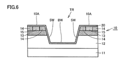
- this step (S60) referring to FIG. 6, the surface (main surface 10A, side wall surface SW, and bottom surface BW) of SiC layer 10 on which the impurity regions (body region 13, source region 14 and contact region 15) are formed.
- the impurity regions body region 13, source region 14 and contact region 15
- the first carbon layer 20 is formed on the surface.
- silicon is selectively removed by reacting a halogen element with silicon constituting SiC layer 10. More specifically, silicon may be selectively removed from the surface of the SiC layer 10 by heating the SiC layer 10 in an atmosphere containing a gas containing a halogen element, or plasma containing a halogen element. Silicon may be selectively removed from the surface of SiC layer 10 by holding SiC layer 10 therein. Thereby, silicon is selectively removed from main surface 10A of SiC layer 10 and side wall surface SW and bottom surface BW of trench TR, and the surface is transformed into first carbon layer 20.
- the first carbon layer 20 is formed so as to have a thickness of 10 nm to 50 nm.
- the thickness of the first carbon layer 20 is preferably 10 nm or more and 100 nm or less, and more preferably 20 nm or more and 50 nm or less.
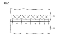
- FIG. 7 schematically shows the bonding state of carbon atoms at the interface between the first carbon layer 20 and the SiC layer 10.
- carbon atoms are indicated by “C”
- bonds between carbon atoms are indicated by straight lines connecting “C”.
- First carbon layer 20 is formed by altering the surface of SiC layer 10 as described above. Therefore, the carbon atoms constituting the first carbon layer 20 and the carbon atoms constituting the SiC layer 10 are in an atomically bonded state over the entire interface. Thereby, the surface of SiC layer 10 is reliably protected by first carbon layer 20.
- the first carbon layer 20 has, for example, a graphene structure, a diamond structure, a DLC structure, or the like.
- a second carbon layer forming step is performed as a step (S70).
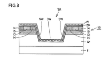
- a resist material is applied onto first carbon layer 20 by, eg, spin coating, and a resist film (not shown) is formed on first carbon layer 20. It is formed.
- the resist film is carbonized by heating the resist film at a temperature of 800 ° C. or higher and 1000 ° C. or lower (for example, 900 ° C.). Thereby, the second carbon layer 21 made of a single layer is formed on the first carbon layer 20.
- the second carbon layer 21 is formed so that the thickness is 50 nm or more and 2000 nm or less.
- the thickness of the 2nd carbon layer 21 becomes like this. Preferably they are 100 nm or more and 1500 nm or less, More preferably, they are 200 nm or more and 1000 nm or less.
- the first and second carbon layers 21 are formed so that the total thickness of the first carbon layer 20 and the second carbon layer 21 is 60 nm or more and 2 ⁇ m or less.
- the total thickness of the first carbon layer 20 and the second carbon layer 21 is preferably 100 nm to 1500 nm, and preferably 200 nm to 1000 nm.
- the first carbon layer 20 is formed to have a higher density than the second carbon layer 21.
- the second carbon layer 21 may be formed by the method of carbonizing the resist film as described above, but is not limited thereto.
- Second carbon layer 21 may be formed by a CVD method or a sputtering method using a hydrocarbon gas such as ethylene (C 2 H 6 ) or propane (C 3 H 8 ).
- an activation annealing step is performed as a step (S80).
- SiC layer 10 on which first carbon layer 20 and second carbon layer 21 are formed is heated at a predetermined temperature.
- the impurities introduced in the steps (S30) and (S50) are activated, and desired carriers are generated in the impurity regions.
- SiC layer 10 may be heated by holding at a temperature of 1600 ° C. or higher and 1900 ° C. or lower for a period of 2 minutes or more and 5 minutes or less.
- the heating temperature of SiC layer 10 is preferably 1800 ° C. or higher and 1900 ° C. or lower.
- FIG. 9 is a graph showing the heating pattern of the SiC layer in steps (S70) and (S80), where the horizontal axis indicates time and the vertical axis indicates temperature.
- the SiC layer may be continuously heated after carbonizing the resist film in step (S70) to form the second carbon layer. More specifically, in step (S70), the temperature is raised to the resist film heating temperature (temperature T 1 ), the SiC layer is held at temperature T 1 and carbonization of the resist film is completed, and then the temperature is lowered to room temperature. activation annealing process allowed to warm to temperature T 2 may be carried out without causing.
- the heating pattern of a SiC layer is not limited to said case, The heating pattern which is once cooled to room temperature after completion
- a carbon layer removing step is performed as a step (S90).
- the first and second carbon layers 20, 21 formed in the above steps (S60) and (S70) are removed by being oxidized. More specifically, for example, the first and second carbon layers 20 and 21 are removed by heating the first and second carbon layers 20 and 21 in an atmosphere containing oxygen (O 2 ).
- the removal of the carbon layer by this oxidation can be performed simultaneously or continuously with the sacrificial oxidation treatment of the SiC layer 10 and the gate oxide film formation step (S100) described later.
- a gate oxide film forming step is performed as a step (S100).
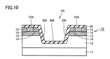
- SiC layer 10 is heated, for example, in an atmosphere containing oxygen (O 2 ).
- gate oxide film 30 is formed along main surface 10A of SiC layer 10 and side wall surface SW and bottom surface BW of trench TR.
- gate electrode 40 made of polysilicon is formed so as to fill trench TR, for example, by LP (Low Pressure) -CVD.
- interlayer insulation film formation process is implemented as process (S120).
- process (S120) referring to FIG. 12, interlayer insulating film 50 made of SiO 2 is formed so as to surround gate electrode 40 together with gate oxide film 30 by, for example, P (Plasma) -CVD.
- an ohmic electrode forming step is performed as a step (S130).
- step (S130) referring to FIG. 12, first, interlayer insulating film 50 and gate oxide film 30 are removed in the region where source electrode 60 is to be formed. In the region, a film made of nickel (Ni), for example, is formed. On the other hand, a film made of Ni is formed on main surface 11B opposite to main surface 11A of SiC substrate 11. Thereafter, an alloying heat treatment is performed, and at least a part of the Ni film is silicided, whereby the source electrode 60 and the drain electrode 70 are formed.
- Ni nickel
- a wiring formation step is performed as a step (S140).
- step (S140) referring to FIG. 13, source wiring 61 made of a conductor such as Al or gold (Au) is formed so as to cover interlayer insulating film 50 and source electrode 60, for example, by vapor deposition. .
- a back surface protection electrode 71 made of a conductor such as Al or Au is formed on the drain electrode 70.
- the surface is removed by selectively removing silicon from the surface (main surface 10A, side wall surface SW, bottom surface BW) of SiC layer 10.
- First carbon layer 20 is formed.
- the surface of SiC layer 10 can be reliably protected by first carbon layer 20.
- the second carbon layer 21 is formed on the first carbon layer 20, and then the SiC layer 10 is heated (activation annealing).
- activation annealing the SiC layer 10 is heated (activation annealing).
- activation annealing can be performed in a state in which a decrease in manufacturing efficiency is suppressed and the surface of SiC layer 10 is more reliably protected. .
- FIG. 14 is a diagram showing a structure of a region to be the termination region of the SiC semiconductor device in the present embodiment
- FIG. 15 is a diagram showing a structure of a region to be the termination region of the SiC semiconductor device in the comparative example.
- SiC layers 10 and 100 include drift regions 12 and 120, body regions 13 and 130 and source regions 14 and 140, and a JTE (Junction Termination Extension) region 16 as an electric field relaxation region, 160 and guard ring regions 17 and 170 are formed.
- the first carbon layer 20 is formed on the surface by selectively removing silicon from the surface of the SiC layer 10 (FIG.
- FIGS. 14 and 15 in the comparative example, the thickness of the resist film is relatively thin at the step portion, and thus it is difficult to sufficiently cover the surface of SiC layer 100 at the step portion with first carbon layer 200. It is.
- the surface of the SiC layer 10 can be sufficiently covered with the first carbon layer 20 even in the stepped portion.
- the surface can be reliably covered with the carbon layer.
- the SiC substrate 11 having a maximum width of 100 mm or more may be prepared. Further, irregularities of 0.5 ⁇ m or more may be formed on the surface (main surface 10A, side wall surface SW, bottom surface BW) of SiC layer 10 formed on SiC substrate 11.
- the first carbon layer 20 is formed by selectively removing silicon from the surface of the SiC layer 10, and the second carbon is obtained by carbonizing a resist film on the first carbon layer 20. A carbon layer 21 is formed. Therefore, the surface of SiC layer 10 can be reliably protected even when the substrate size is large and the surface irregularities are large.
- a second carbon layer 21 composed of a plurality of laminated carbon layers 22, 23, 24 is formed on the first carbon layer 20.
- the first laminated carbon layer 22 is formed by a CVD method using a hydrocarbon gas such as ethylene gas or propane gas
- the second laminated carbon layer 23 is formed by a sputtering method
- the third laminated carbon layer is formed.
- 24 is formed by a method of carbonizing the resist film. Therefore, the laminated carbon layers 22 to 24 are formed such that the laminated carbon layers close to the surface in the direction perpendicular to the surface (main surface 10A, side wall surface SW, bottom surface BW) of SiC layer 10 have a relatively high density. Is done.
- the present invention is not limited to this.
- the number of layers is not particularly limited as long as the second carbon layer 21 is composed of a plurality of layers (two or more layers), and the method of forming each laminated carbon layer is also the above method (method of carbonizing a resist film, CVD Method and sputtering method).
- a method for manufacturing a silicon carbide semiconductor device of the present invention is a silicon carbide semiconductor that is required to perform activation annealing in a state where the surface of the silicon carbide layer is more reliably protected while suppressing a decrease in manufacturing efficiency. In the manufacturing method of the device, it can be applied particularly advantageously.
Landscapes
- Electrodes Of Semiconductors (AREA)
- Physics & Mathematics (AREA)
- Engineering & Computer Science (AREA)
- Plasma & Fusion (AREA)
- Chemical & Material Sciences (AREA)
- Crystallography & Structural Chemistry (AREA)
Abstract
SiC半導体装置の製造方法は、SiC層(10)に不純物領域(ボディ領域13、ソース領域14、コンタクト領域15)を形成する工程と、不純物領域が形成されたSiC層(10)の表面(主面,側壁面SW,底面BW)から珪素を選択的に除去することにより、上記表面に第1炭素層(20)を形成する工程と、第1炭素層(20)の上に第2炭素層(21)を形成する工程と、第1炭素層(20)および第2炭素層(21)が形成されたSiC層(10)を加熱する工程とを備えている。
Description
本発明は、炭化珪素半導体装置の製造方法に関し、より特定的には、製造効率の低下を抑制し、かつ、炭化珪素層の表面がより確実に保護された状態で活性化アニールを実施することが可能な炭化珪素半導体装置の製造方法に関する。
近年、半導体装置の高耐圧化、低損失化、高温環境下での使用などを可能とするため、半導体装置を構成する材料として炭化珪素の採用が進められつつある。炭化珪素は、従来から半導体装置を構成する材料として広く使用されている珪素に比べてバンドギャップが大きいワイドバンドギャップ半導体である。そのため、半導体装置を構成する材料として炭化珪素を採用することにより、半導体装置の高耐圧化、オン抵抗の低減などを達成することができる。また、炭化珪素を材料として採用した半導体装置は、珪素を材料として採用した半導体装置に比べて、高温環境下で使用された場合の特性の低下が小さいという利点も有している。
炭化珪素を材料として用いた半導体装置の製造プロセスでは、イオン注入などにより炭化珪素層内に不純物が導入され、その後活性化アニールが実施される。これにより、炭化珪素層内の不純物領域において所望のキャリアが生成する。この活性化アニールはたとえば1500℃を超える高温で実施されるため、加熱による炭化珪素層の表面荒れを抑制することが必要になる。これに対して、炭化珪素層の表面に炭素層が堆積された状態で活性化アニールを実施するプロセスが提案されている(たとえば特開2001-68428号公報(特許文献1)および特開2013-26372号公報(特許文献2)参照)。
特許文献1では、ダイヤモンドライクカーボン(DLC:Diamond Like Carbon)膜やフォトレジスト膜を炭化させた膜をエピタキシャル成長層(炭化珪素層)の表面に堆積させた状態で活性化アニールするプロセスが開示されている。また、特許文献2では、炭化珪素層の表層部から珪素を選択的に除去することにより炭素層を形成し、その後活性化アニールするプロセスが開示されている。
上記特許文献1に開示されているプロセスでは、CVD(Chemical Vapor Deposition)法やスパッタリング法などの方法により炭化珪素層の表面に炭素層が形成される。しかし、CVD法では炭化珪素層の表面における段差や凹凸が大きい場合に膜のカバレッジが悪くなり、スパッタリング法では膜の密着性が低く割れが発生し易いという問題がある。また、フォトレジスト膜を炭化させた膜を形成する場合には、面内における膜厚のばらつきが大きくなる(膜厚分布が悪くなる)という問題がある。そのため、これらの方法では炭化珪素層の表面を十分に保護した状態で活性化アニールを実施することが困難である。
また、上記特許文献2に開示されているプロセスでは、炭化珪素層の表層部を変質させることにより炭素層が形成される。そのため、このプロセスでは炭化珪素層の表層部に形成された不純物領域の一部が当該炭素層の形成により消費される。よって、このプロセスでは炭素層の形成による消費を見込んで不純物領域をより深く形成しておく必要があり、その結果製造効率が低下するという問題がある。
本発明は、上記課題に鑑みてなされたものであり、その目的は、製造効率の低下を抑制し、かつ、炭化珪素層の表面がより確実に保護された状態で活性化アニールを実施することが可能な炭化珪素半導体装置の製造方法を提供することである。
本発明に従った炭化珪素半導体装置の製造方法は、炭化珪素層に不純物領域を形成する工程と、不純物領域が形成された炭化珪素層の表面から珪素を選択的に除去することにより、上記表面に第1炭素層を形成する工程と、第1炭素層の上に第2炭素層を形成する工程と、第1炭素層および第2炭素層が形成された炭化珪素層を加熱する工程とを備えている。
本発明に従った炭化珪素半導体装置の製造方法によれば、製造効率の低下を抑制し、かつ、炭化珪素層の表面がより確実に保護された状態で活性化アニールを実施することができる。
[本願発明の実施形態の説明]
まず、本発明の実施形態の内容を列記して説明する。
まず、本発明の実施形態の内容を列記して説明する。
(1)本実施形態に係る炭化珪素半導体装置の製造方法は、炭化珪素層(10)に不純物領域(13,14,15)を形成する工程と、不純物領域が形成された炭化珪素層の表面(10A,SW,BW)から珪素を選択的に除去することにより、上記表面に第1炭素層(20)を形成する工程と、第1炭素層の上に第2炭素層(21)を形成する工程と、第1炭素層および第2炭素層が形成された炭化珪素層を加熱する工程とを備えている。
本実施形態に係る炭化珪素半導体装置の製造方法では、まず、炭化珪素層の表面から珪素を選択的に除去することにより、上記表面に第1炭素層が形成される。これにより、炭化珪素層の表面を第1炭素層により確実に保護することができる。次に、第1炭素層の上に第2炭素層が形成され、その後炭化珪素層が加熱される(活性化アニール)。これにより、第1炭素層の厚みを小さくして炭素層による不純物領域の消費を抑えた場合でも、第1炭素層および第2炭素層の合計として必要な炭素層の厚みを確保することができる。そのため、第1炭素層を厚く形成して不純物領域が多く消費されることによる製造効率の低下を抑制することができる。したがって、本実施形態に係る炭化珪素半導体装置の製造方法によれば、製造効率の低下を抑制し、かつ、炭化珪素層の表面がより確実に保護された状態で活性化アニールを実施することができる。
ここで、「炭化珪素層の表面から珪素が選択的に除去される状態」とは、炭化珪素を構成する炭素原子に比べて珪素原子が多く離脱する状態を意味し、たとえば炭素原子の10倍以上の割合で珪素原子が炭化珪素層の表面から離脱する状態が含まれる。
(2)上記炭化珪素半導体装置の製造方法において、第1炭素層を形成する工程では、第2炭素層よりも高密度になるように第1炭素層が形成されてもよい。
これにより、炭化珪素層の表面がさらに確実に保護された状態で活性化アニールを実施することができる。その結果、活性化アニールによる炭化珪素層の表面荒れを抑制することができる。
(3)上記炭化珪素半導体装置の製造方法において、第2炭素層を形成する工程では、単一層から構成される第2炭素層が形成されてもよい。
これにより、複数層から構成される第2炭素層を形成する場合に比べてプロセスをより簡略化することができる。その結果、製造効率をより向上させることができる。
(4)上記炭化珪素半導体装置の製造方法において、第2炭素層を形成する工程では、複数層から構成される第2炭素層が形成されてもよい。
これにより、単一層から構成される第2炭素層を形成する場合に比べてより緻密な第2炭素層を形成することができる。その結果、炭化珪素層の表面が一層確実に保護された状態で活性化アニールを実施することができる。
(5)上記炭化珪素半導体装置の製造方法において、複数層を構成する複数の積層炭素層(22,23,24)は、炭化珪素層の上記表面に近い積層炭素層が相対的に高密度になるように形成されてもよい。
これにより、炭化珪素層の表面が一層確実に保護された状態で活性化アニールを実施することができる。その結果、活性化アニールによる炭化珪素層の表面荒れをより効果的に抑制することができる。
(6)上記炭化珪素半導体装置の製造方法において、第2炭素層は、レジスト膜を炭化させる方法、CVD法およびスパッタリング法からなる群より選択される少なくともいずれか一の方法により形成されてもよい。
このように、第2炭素層は第1炭素層を形成する方法とは異なる種々の方法を用いて形成することができる。
(7)上記炭化珪素半導体装置の製造方法において、第2炭素層を形成する工程では、800℃以上1000℃以下の温度でレジスト膜を加熱して炭化させることにより第2炭素層が形成されてもよい。
上記加熱温度が800℃未満である場合には、レジスト膜を十分に炭化させることが困難である。一方で、上記加熱温度が800℃以上であれば1000℃以下であってもレジスト膜を十分に炭化させることができる。そのため、レジスト膜の加熱温度は800℃以上1000℃以下であることが好ましい。
(8)上記炭化珪素半導体装置の製造方法において、炭化珪素層を加熱する工程では、第2炭素層を形成する工程においてレジスト膜の炭化が完了した後に連続して炭化珪素層が加熱されてもよい。
これにより、レジスト膜の炭化が完了した後に一旦冷却される場合に比べて製造効率をより向上させることができる。
(9)上記炭化珪素半導体装置の製造方法において、炭化珪素層を加熱する工程では、1600℃以上1900℃以下の温度で炭化珪素層が加熱されてもよい。
上記加熱温度が1600℃未満である場合には、炭化珪素層内の不純物領域において十分にキャリアを発生させることが困難である。一方で、上記加熱温度が1900℃を超える場合には、加熱により炭化珪素層が損傷を受ける懸念がある。そのため、炭化珪素層の加熱温度は1600℃以上1900℃以下であることが好ましい。
(10)上記炭化珪素半導体装置の製造方法において、第1炭素層を形成する工程では、10nm以上50nm以下の厚みを有する第1炭素層が形成されてもよい。
上記厚みが10nm未満である場合には、炭化珪素層の表面が確実に保護された状態で活性化アニールを実施することが困難になる。一方で、上記厚みが50nmを超える場合には、第1炭素層の形成による不純物領域の消費が多くなり、製造効率が低下する。そのため、第1炭素層は10nm以上50nm以下の厚みで形成されることが好ましい。
(11)上記炭化珪素半導体装置の製造方法において、第2炭素層を形成する工程では、50nm以上の厚みを有する第2炭素層が形成されてもよい。
上記厚みが50nm未満である場合には、第1炭素層の上を十分に覆うことが困難になり、当該第1炭素層の耐久性を十分に確保することが困難になる。そのため、第2炭素層は50nm以上の厚みで形成されることが好ましい。
(12)上記炭化珪素半導体装置の製造方法において、第1炭素層を形成する工程および第2炭素層を形成する工程では、第1炭素層および第2炭素層の合計の厚みが1μm以下になるように第1炭素層および第2炭素層が形成されてもよい。
上記合計の厚みが1μmを超える場合には炭素層の形成に長時間を要し、また上記合計の厚みが1μm以下でも炭化珪素層の表面を十分に保護することが可能である。そのため、第1炭素層および第2炭素層は合計の厚みが1μm以下で形成されることが好ましい。
(13)上記炭化珪素半導体装置の製造方法において、第1炭素層を形成する工程では、ハロゲン元素と珪素とを反応させることにより、炭化珪素層の上記表面から珪素が選択的に除去されてもよい。
これにより、炭化珪素層の上記表面から珪素を効率良く離脱させることができる。
(14)上記炭化珪素半導体装置の製造方法において、第1炭素層を形成する工程では、ハロゲン元素を含有するガスを含む雰囲気中において炭化珪素層が加熱されることにより、炭化珪素層の上記表面から珪素が選択的に除去されてもよい。
(14)上記炭化珪素半導体装置の製造方法において、第1炭素層を形成する工程では、ハロゲン元素を含有するガスを含む雰囲気中において炭化珪素層が加熱されることにより、炭化珪素層の上記表面から珪素が選択的に除去されてもよい。
これにより、ハロゲン元素を用いて珪素を除去して第1炭素層を形成することが容易になる。また、「ハロゲン元素を含有するガス」としては、たとえば塩素(Cl2)ガス、フッ素(F2)ガス、臭素(Br2)ガス、ヨウ素(I2)ガス、塩化水素(HCl)ガス、三塩化硼素(BCl3)ガス、六フッ化硫黄(SF6)ガス、四フッ化炭素(CF4)ガスなどを採用することができる。
(15)上記炭化珪素半導体装置の製造方法において、第1炭素層を形成する工程では、ハロゲン元素を含むプラズマ中において炭化珪素層が保持されることにより、炭化珪素層の上記表面から珪素が選択的に除去されてもよい。
これにより、ハロゲン元素を用いて珪素を除去して第1炭素層を形成することがより容易になる。また、「ハロゲン元素を含むプラズマ」としては、たとえば塩素(Cl)、フッ素(F)、臭素(Br)、ヨウ素(I)からなる群より選択される一以上の元素を含むプラズマを採用することができる。
(16)上記炭化珪素半導体装置の製造方法は、炭化珪素層を加熱する工程の後、第1炭素層および第2炭素層を除去する工程をさらに備えていてもよい。
これにより、第1炭素層および第2炭素層が除去された後の炭化珪素層の表面上にゲート酸化膜を形成することができる。
(17)上記炭化珪素半導体装置の製造方法において、炭化珪素層の上記表面は、(000-1)面に対するオフ角が8°以下である主面(10A)を含んでいてもよい。
これにより、炭化珪素層の上記表面から珪素を除去することにより第1炭素層を形成する速度がより向上する。その結果、製造効率をより向上させることができる。
[本願発明の実施形態の詳細]
次に、本発明の実施形態の具体例を図面を参照しつつ説明する。なお、以下の図面において同一または相当する部分には同一の参照番号を付し、その説明は繰り返さない。また、本明細書中においては、個別方位を[]、集合方位を<>、個別面を()、集合面を{}でそれぞれ示す。また、負の指数については、結晶学上、”-”(バー)を数字の上に付けることになっているが、本明細書中では、数字の前に負の符号を付けている。
次に、本発明の実施形態の具体例を図面を参照しつつ説明する。なお、以下の図面において同一または相当する部分には同一の参照番号を付し、その説明は繰り返さない。また、本明細書中においては、個別方位を[]、集合方位を<>、個別面を()、集合面を{}でそれぞれ示す。また、負の指数については、結晶学上、”-”(バー)を数字の上に付けることになっているが、本明細書中では、数字の前に負の符号を付けている。
(実施形態1)
まず、本発明の一実施形態である実施形態1に係る炭化珪素(SiC)半導体装置の製造方法について説明する。図1を参照して、本実施形態に係るSiC半導体装置の製造方法では、まず、工程(S10)として炭化珪素(SiC)基板準備工程が実施される。この工程(S10)では、図2を参照して、たとえば4H-SiCからなるインゴット(図示しない)を切断し、研磨処理などを行うことにより、SiC基板11が準備される。
まず、本発明の一実施形態である実施形態1に係る炭化珪素(SiC)半導体装置の製造方法について説明する。図1を参照して、本実施形態に係るSiC半導体装置の製造方法では、まず、工程(S10)として炭化珪素(SiC)基板準備工程が実施される。この工程(S10)では、図2を参照して、たとえば4H-SiCからなるインゴット(図示しない)を切断し、研磨処理などを行うことにより、SiC基板11が準備される。
SiC基板11の主面11Aは、(000-1)面に対して8°以下のオフ角、好ましくは4°以下のオフ角を有している。また、SiC基板11の幅の最大値は、たとえば100mm以上である。
次に、工程(S20)として炭化珪素(SiC)層形成工程が実施される。この工程(S20)では、図2を参照して、SiC基板11の一方の主面11A上においてエピタキシャル成長によりSiC層10が形成される。SiC層10の主面10Aは、(000-1)面に対して8°以下のオフ角、好ましくは4°以下のオフ角を有している。また、SiC層10の主面10Aには0.5μm以上の凹凸(たとえばメサ構造など)が形成されている。なお、「凹凸が0.5μm以上」とは、主面10A全体において高低差の最大値が0.5μm以上であることを意味する。
次に、工程(S30)としてソース/ボディ領域形成工程が実施される。この工程(S30)では、図3を参照して、まず、たとえばアルミニウム(Al)イオンが主面10A側からSiC層10内に注入されることにより、当該SiC層10内に導電型がp型であるボディ領域13が形成される。次に、たとえばリン(P)イオンが上記Alイオンよりも浅い深さでSiC層10内に注入されることにより、当該SiC層10内において導電型がn型であるソース領域14が形成される。そして、SiC層10においてボディ領域13およびソース領域14のいずれも形成されない領域がドリフト領域12になる。
次に、工程(S40)としてトレンチ形成工程が実施される。この工程(S40)では、まず、SiC層10の主面10A上において開口部を有する二酸化珪素(SiO2)からなるマスク(図示しない)が形成される。そして、当該マスクを用いたRIE(Reactive Ion Etching)などのドライエッチング、または塩素(Cl2)などのハロゲン系ガスを用いた熱エッチング、あるいはそれらの組み合わせなどの方法によりトレンチTRが形成される。トレンチTRは側壁面SWおよび底面BWを有し、ソース領域14およびボディ領域13を貫通してドリフト領域12に到達するように形成される。すなわち、トレンチTRは、側壁面SWがドリフト領域12、ボディ領域13およびソース領域14を露出させ、底面BWがドリフト領域12内に位置するように形成される。トレンチTRは、SiC層10の主面10Aに沿った方向(図4中の紙面奥行き方向)に延在するように形成される。また、トレンチTRは、たとえば(03-38)面からなる側壁面SWを有するように形成される。
次に、工程(S50)としてコンタクト領域形成工程が実施される。この工程(S50)では、図5を参照して、たとえばAlイオンがソース領域14内に注入されることにより、当該ソース領域14内にコンタクト領域15が形成される。このイオン注入は、たとえばSiC層10の主面10A上においてイオン注入すべき所望の領域に開口部を有するマスク(図示しない)を形成した後に実施することができる。このようにしてSiC層10において不純物領域(ボディ領域13、ソース領域14およびコンタクト領域15)が形成される。
次に、工程(S60)として第1炭素層形成工程が実施される。この工程(S60)では、図6を参照して、不純物領域(ボディ領域13、ソース領域14およびコンタクト領域15)が形成されたSiC層10の表面(主面10A、側壁面SWおよび底面BW)から珪素が選択的に除去されることにより、上記表面に第1炭素層20が形成される。
この工程(S60)では、ハロゲン元素とSiC層10を構成する珪素とを反応させることにより珪素が選択的に除去される。より具体的には、ハロゲン元素を含有するガスを含む雰囲気中においてSiC層10が加熱されることによりSiC層10の上記表面から珪素が選択的に除去されてもよいし、ハロゲン元素を含むプラズマ中においてSiC層10が保持されることによりSiC層10の上記表面から珪素が選択的に除去されてもよい。これにより、SiC層10の主面10AならびにトレンチTRの側壁面SWおよび底面BWから珪素が選択的に除去され、上記表面が第1炭素層20に変質する。
この工程(S60)では、厚みが10nm以上50nm以下になるように第1炭素層20が形成される。第1炭素層20の厚みは、好ましくは10nm以上100nm以下であり、より好ましくは20nm以上50nm以下である。
図7は、第1炭素層20とSiC層10との界面における炭素原子の結合状態を模式的に示したものである。図7中において、炭素原子が「C」により示され、炭素原子間の結合が「C」同士を結ぶ直線により示されている。第1炭素層20は、上述のようにSiC層10の上記表面を変質させることにより形成される。そのため、第1炭素層20を構成する炭素原子とSiC層10を構成する炭素原子とは界面全体に亘り原子的に結合された状態となっている。これにより、SiC層10の上記表面は第1炭素層20により確実に保護された状態となっている。第1炭素層20は、たとえばグラフェン構造、ダイヤモンド構造またはDLC構造などを有している。
次に、工程(S70)として第2炭素層形成工程が実施される。この工程(S70)では、図8を参照して、たとえばスピンコート法などにより第1炭素層20の上にレジスト材料が塗布され、当該第1炭素層20の上にレジスト膜(図示しない)が形成される。次に、レジスト膜を800℃以上1000℃以下の温度(たとえば900℃)で加熱することにより当該レジスト膜が炭化する。これにより、第1炭素層20の上に単一層からなる第2炭素層21が形成される。
この工程(S70)では、厚みが50nm以上2000nm以下になるように第2炭素層21が形成される。第2炭素層21の厚みは、好ましくは100nm以上1500nm以下であり、より好ましくは200nm以上1000nm以下である。
工程(S60)および(S70)では、第1炭素層20および第2炭素層21の合計の厚みが60nm以上2μm以下になるように当該第1および第2炭素層21が形成される。第1炭素層20および第2炭素層21の合計の厚みは、好ましくは100nm以上1500nm以下であり、好ましくは200nm以上1000nm以下である。また、第1炭素層20は、第2炭素層21よりも高密度になるように形成される。
この工程(S70)では、上述のようにレジスト膜を炭化させる方法により第2炭素層21が形成されてもよいが、これに限定されるものではない。第2炭素層21は、たとえばエチレン(C2H6)やプロパン(C3H8)などの炭化水素のガスを用いたCVD法やスパッタリング法などの方法により形成されてもよい。
次に、工程(S80)として活性化アニール工程が実施される。この工程(S80)では、図8を参照して、第1炭素層20および第2炭素層21が形成されたSiC層10が所定温度で加熱される。これにより、上記工程(S30)および(S50)において導入された不純物が活性化し、不純物領域において所望のキャリアが発生する。
この工程(S80)では、1600℃以上1900℃以下の温度で2分間以上5分間以下の時間保持されることによりSiC層10が加熱されてもよい。SiC層10の加熱温度は、好ましくは1800℃以上1900℃以下である。
図9は、工程(S70)および(S80)におけるSiC層の加熱パターンを示すグラフであり、横軸が時間を示し、縦軸が温度を示している。図9を参照して、この工程(S80)では、工程(S70)においてレジスト膜を炭化させて第2炭素層を形成した後、連続してSiC層が加熱されてもよい。より具体的には、工程(S70)においてレジスト膜の加熱温度(温度T1)にまで昇温させ、温度T1においてSiC層を保持してレジスト膜の炭化が完了した後、室温にまで降温させずに温度T2にまで昇温させて活性化アニール処理が実施されてもよい。なお、SiC層の加熱パターンは上記の場合に限定されず、工程(S70)が完了した後に一旦室温にまで冷却され、その後工程(S80)が実施される加熱パターンが用いられてもよい。
次に、工程(S90)として炭素層除去工程が実施される。この工程(S90)では、上記工程(S60)および(S70)において形成された第1および第2炭素層20,21が酸化されることにより除去される。より具体的には、たとえば酸素(O2)を含む雰囲気中において第1および第2炭素層20,21を加熱することにより、当該第1および第2炭素層20,21が除去される。この酸化による炭素層の除去は、SiC層10の犠牲酸化処理や後述するゲート酸化膜形成工程(S100)と同時または連続的に実施することができる。
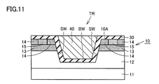
次に、工程(S100)としてゲート酸化膜形成工程が実施される。この工程(S100)では、図10を参照して、たとえば酸素(O2)を含む雰囲気中においてSiC層10が加熱される。これにより、SiC層10の主面10AならびにトレンチTRの側壁面SWおよび底面BW上に沿うようにゲート酸化膜30が形成される。
次に、工程(S110)としてゲート電極形成工程が実施される。この工程(S110)では、図11を参照して、たとえばLP(Low Pressure)-CVD法により、トレンチTRを充填するようにポリシリコンからなるゲート電極40が形成される。
次に、工程(S120)として層間絶縁膜形成工程が実施される。この工程(S120)では、図12を参照して、たとえばP(Plasma)-CVD法により、SiO2からなる層間絶縁膜50がゲート酸化膜30とともにゲート電極40を取り囲むように形成される。
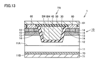
次に、工程(S130)としてオーミック電極形成工程が実施される。この工程(S130)では、図12を参照して、まずソース電極60を形成すべき領域において、層間絶縁膜50およびゲート酸化膜30が除去される。そして、当該領域において、たとえばニッケル(Ni)からなる膜が形成される。一方、SiC基板11の主面11Aとは反対側の主面11B上においてNiからなる膜が形成される。その後、合金化熱処理が実施され、上記Niからなる膜の少なくとも一部がシリサイド化することによりソース電極60およびドレイン電極70が形成される。
次に、工程(S140)として配線形成工程が実施される。この工程(S140)では、図13を参照して、たとえば蒸着法によりAlや金(Au)などの導電体からなるソース配線61が、層間絶縁膜50およびソース電極60を覆うように形成される。また、AlやAuなどの導電体からなる裏面保護電極71がドレイン電極70上に形成される。以上の工程(S10)~(S140)が実施されることによりMOSFET1(SiC半導体装置)が製造され、本実施形態に係るSiC半導体装置の製造方法が完了する。
以上のように、本実施形態に係るSiC半導体装置の製造方法では、まず、SiC層10の表面(主面10A、側壁面SW、底面BW)から珪素を選択的に除去することにより、上記表面に第1炭素層20が形成される。これにより、SiC層10の表面を第1炭素層20により確実に保護することができる。次に、第1炭素層20の上に第2炭素層21が形成され、その後SiC層10が加熱される(活性化アニール)。これにより、第1炭素層20の厚みを小さくして炭素層による不純物領域の消費を抑えた場合でも、第1炭素層20および第2炭素層21の合計として必要な炭素層の厚みを確保することができる。そのため、第1炭素層20を厚く形成して不純物領域が多く消費されることによる製造効率の低下を抑制することができる。したがって、本実施形態に係るSiC半導体装置の製造方法によれば、製造効率の低下を抑制し、かつ、SiC層10の表面がより確実に保護された状態で活性化アニールを実施することができる。
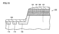
図14は、本実施形態におけるSiC半導体装置の終端領域となるべき領域の構造を示す図であり、図15は比較例におけるSiC半導体装置の終端領域となるべき領域の構造を示す図である。図14および図15を参照して、SiC層10,100にはドリフト領域12,120、ボディ領域13,130およびソース領域14,140、ならびに電界緩和領域としてのJTE(Junction Termination Extension)領域16,160およびガードリング領域17,170が形成されている。また、本実施形態ではSiC層10の表面から珪素を選択的に除去することにより上記表面に第1炭素層20が形成されており(図14)、一方で比較例ではSiC層100の表面上にスピンコート法によりレジスト膜を形成し、当該レジスト膜を炭化させることにより第1炭素層200が形成されている(図15)。図14および図15に示すように、比較例では段差部においてレジスト膜の厚みが相対的に薄くなるため、当該段差部におけるSiC層100の表面を第1炭素層200により十分に覆うことが困難である。一方で、本実施形態では段差部においてもSiC層10の表面を第1炭素層20により十分に覆うことができる。このように本実施形態では、SiC層10の表面に段差や凹凸が存在する場合でも上記表面を炭素層により確実に覆うことができる。
上記炭化珪素半導体装置の製造方法において、SiC基板準備工程(S10)では、幅の最大値が100mm以上であるSiC基板11が準備されてもよい。また、SiC基板11上に形成されるSiC層10の表面(主面10A、側壁面SW、底面BW)には0.5μm以上の凹凸が形成されていてもよい。
このように基板サイズが大きい場合には、スピンコート法によりレジスト膜を塗布し、当該レジスト膜を炭化させて第1炭素層を形成すると膜厚のばらつきが大きくなる(中央部の膜厚が小さく外周部の膜厚が大きくなる)。また、SiC層10の表面の凹凸が大きい場合には、スピンコート法により形成されるレジスト膜により表面全体を十分に覆うことは困難である。これに対して、本実施形態ではSiC層10の表面から珪素を選択的に除去することにより第1炭素層20が形成され、当該第1炭素層20の上にレジスト膜を炭化させた第2炭素層21が形成される。そのため、基板サイズが大きく表面の凹凸が大きい場合でもSiC層10の表面を確実に保護することができる。
(実施形態2)
次に、本発明の他の実施形態である実施形態2について説明する。本実施形態に係るSiC半導体装置の製造方法は、基本的には上記実施形態1の場合と同様に実施され、かつ同様の効果を奏する。しかし、本実施形態に係るSiC半導体装置の製造方法は、第2炭素層形成工程において上記実施形態1の場合とは異なっている。
次に、本発明の他の実施形態である実施形態2について説明する。本実施形態に係るSiC半導体装置の製造方法は、基本的には上記実施形態1の場合と同様に実施され、かつ同様の効果を奏する。しかし、本実施形態に係るSiC半導体装置の製造方法は、第2炭素層形成工程において上記実施形態1の場合とは異なっている。
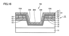
図16を参照して、本実施形態では複数の積層炭素層22,23,24から構成される第2炭素層21が第1炭素層20上に形成される。より具体的には、第1積層炭素層22はエチレンガスまたはプロパンガスなどの炭化水素ガスを用いたCVD法により形成され、第2積層炭素層23はスパッタリング法により形成され、第3積層炭素層24はレジスト膜を炭化させる方法により形成される。そのため、積層炭素層22~24は、SiC層10の表面(主面10A、側壁面SW、底面BW)に垂直な方向において上記表面に近い積層炭素層が相対的に高密度になるように形成される。このように第2炭素層21を複数層から構成することにより、上記実施形態1のように第2炭素層21を単一層から構成する場合に比べて膜が緻密化され、その結果SiC層10の表面を一層確実に保護することが可能になる。
また、本実施形態では第2炭素層21が3層から構成される場合について説明したが、これに限定されるものではない。第2炭素層21は、複数層(2層以上)で構成されていれば層数は特に限定されず、また各々の積層炭素層を形成する方法も上記方法(レジスト膜を炭化させる方法、CVD法およびスパッタリング法)から任意に選択することが可能である。
今回開示された実施の形態はすべての点で例示であって、制限的なものではないと考えられるべきである。本発明の範囲は上記した説明ではなくて請求の範囲によって示され、請求の範囲と均等の意味、および範囲内でのすべての変更が含まれることが意図される。
本発明の炭化珪素半導体装置の製造方法は、製造効率の低下を抑制し、かつ、炭化珪素層の表面がより確実に保護された状態で活性化アニールを実施することが要求される炭化珪素半導体装置の製造方法において、特に有利に適用され得る。
1 MOSFET、10,100 炭化珪素(SiC)層、10A,11A,11B 主面、11 炭化珪素(SiC)基板、12,120 ドリフト領域、13,130 ボディ領域、14,140 ソース領域、15 コンタクト領域、16,160 JTE領域、17,170 ガードリング領域、20 第1炭素層、21 第2炭素層、22 第1積層炭素層、23 第2積層炭素層、24 第3積層炭素層、30 ゲート酸化膜、40 ゲート電極、50 層間絶縁膜、60 ソース電極、61 ソース配線、70 ドレイン電極、71 裏面保護電極、BW 底面、SW 側壁面、TR トレンチ。
Claims (17)
- 炭化珪素層に不純物領域を形成する工程と、
前記不純物領域が形成された前記炭化珪素層の表面から珪素を選択的に除去することにより、前記表面に第1炭素層を形成する工程と、
前記第1炭素層の上に第2炭素層を形成する工程と、
前記第1炭素層および前記第2炭素層が形成された前記炭化珪素層を加熱する工程とを備える、炭化珪素半導体装置の製造方法。 - 前記第1炭素層を形成する工程では、前記第2炭素層よりも高密度になるように前記第1炭素層が形成される、請求項1に記載の炭化珪素半導体装置の製造方法。
- 前記第2炭素層を形成する工程では、単一層から構成される前記第2炭素層が形成される、請求項1または請求項2に記載の炭化珪素半導体装置の製造方法。
- 前記第2炭素層を形成する工程では、複数層から構成される前記第2炭素層が形成される、請求項1または請求項2に記載の炭化珪素半導体装置の製造方法。
- 前記複数層を構成する複数の積層炭素層は、前記炭化珪素層の前記表面に近い前記積層炭素層が相対的に高密度になるように形成される、請求項4に記載の炭化珪素半導体装置の製造方法。
- 前記第2炭素層は、レジスト膜を炭化させる方法、CVD法およびスパッタリング法からなる群より選択される少なくともいずれか一の方法により形成される、請求項1~請求項5のいずれか1項に記載の炭化珪素半導体装置の製造方法。
- 前記第2炭素層を形成する工程では、800℃以上1000℃以下の温度で前記レジスト膜を加熱して炭化させることにより前記第2炭素層が形成される、請求項6に記載の炭化珪素半導体装置の製造方法。
- 前記炭化珪素層を加熱する工程では、前記第2炭素層を形成する工程において前記レジスト膜の炭化が完了した後に連続して前記炭化珪素層が加熱される、請求項7に記載の炭化珪素半導体装置の製造方法。
- 前記炭化珪素層を加熱する工程では、1600℃以上1900℃以下の温度で前記炭化珪素層が加熱される、請求項1~請求項8のいずれか1項に記載の炭化珪素半導体装置の製造方法。
- 前記第1炭素層を形成する工程では、10nm以上50nm以下の厚みを有する前記第1炭素層が形成される、請求項1~請求項9のいずれか1項に記載の炭化珪素半導体装置の製造方法。
- 前記第2炭素層を形成する工程では、50nm以上の厚みを有する前記第2炭素層が形成される、請求項1~請求項10のいずれか1項に記載の炭化珪素半導体装置の製造方法。
- 前記第1炭素層を形成する工程および前記第2炭素層を形成する工程では、前記第1炭素層および前記第2炭素層の合計の厚みが1μm以下になるように前記第1炭素層および前記第2炭素層が形成される、請求項1~請求項11のいずれか1項に記載の炭化珪素半導体装置の製造方法。
- 前記第1炭素層を形成する工程では、ハロゲン元素と珪素とを反応させることにより、前記炭化珪素層の前記表面から珪素が選択的に除去される、請求項1~請求項12のいずれか1項に記載の炭化珪素半導体装置の製造方法。
- 前記第1炭素層を形成する工程では、ハロゲン元素を含有するガスを含む雰囲気中において前記炭化珪素層が加熱されることにより、前記炭化珪素層の前記表面から珪素が選択的に除去される、請求項13に記載の炭化珪素半導体装置の製造方法。
- 前記第1炭素層を形成する工程では、ハロゲン元素を含むプラズマ中において前記炭化珪素層が保持されることにより、前記炭化珪素層の前記表面から珪素が選択的に除去される、請求項13に記載の炭化珪素半導体装置の製造方法。
- 前記炭化珪素層を加熱する工程の後、前記第1炭素層および前記第2炭素層を除去する工程をさらに備える、請求項1~請求項15のいずれか1項に記載の炭化珪素半導体装置の製造方法。
- 前記炭化珪素層の前記表面は、(000-1)面に対するオフ角が8°以下である主面を含む、請求項1~請求項16のいずれか1項に記載の炭化珪素半導体装置の製造方法。
Priority Applications (1)
| Application Number | Priority Date | Filing Date | Title |
|---|---|---|---|
| US15/024,171 US9659773B2 (en) | 2013-09-25 | 2014-08-11 | Method for manufacturing silicon carbide semiconductor device by selectively removing silicon from silicon carbide substrate to form protective carbon layer on silicon carbide substrate for activating dopants |
Applications Claiming Priority (2)
| Application Number | Priority Date | Filing Date | Title |
|---|---|---|---|
| JP2013198214A JP2015065289A (ja) | 2013-09-25 | 2013-09-25 | 炭化珪素半導体装置の製造方法 |
| JP2013-198214 | 2013-09-25 |
Publications (1)
| Publication Number | Publication Date |
|---|---|
| WO2015045653A1 true WO2015045653A1 (ja) | 2015-04-02 |
Family
ID=52742808
Family Applications (1)
| Application Number | Title | Priority Date | Filing Date |
|---|---|---|---|
| PCT/JP2014/071165 Ceased WO2015045653A1 (ja) | 2013-09-25 | 2014-08-11 | 炭化珪素半導体装置の製造方法 |
Country Status (3)
| Country | Link |
|---|---|
| US (1) | US9659773B2 (ja) |
| JP (1) | JP2015065289A (ja) |
| WO (1) | WO2015045653A1 (ja) |
Cited By (1)
| Publication number | Priority date | Publication date | Assignee | Title |
|---|---|---|---|---|
| JP2024053119A (ja) * | 2017-12-06 | 2024-04-12 | 富士電機株式会社 | 半導体装置及びその製造方法 |
Families Citing this family (3)
| Publication number | Priority date | Publication date | Assignee | Title |
|---|---|---|---|---|
| KR101832882B1 (ko) * | 2015-11-30 | 2018-02-28 | 주식회사 티씨케이 | 탄소 층을 이용한 실리콘 카바이드 구조물 제조방법 |
| CN115799061B (zh) * | 2023-01-09 | 2023-09-05 | 浙江大学杭州国际科创中心 | SiC晶圆切割片加工方法及SiC晶圆切割片加工装置 |
| CN120015636B (zh) * | 2025-04-22 | 2025-07-11 | 无锡邑文微电子科技股份有限公司 | 一种SiC晶圆表面碳保护膜及其制备方法和应用 |
Citations (4)
| Publication number | Priority date | Publication date | Assignee | Title |
|---|---|---|---|---|
| WO2005076327A1 (ja) * | 2004-02-06 | 2005-08-18 | Matsushita Electric Industrial Co., Ltd. | 炭化珪素半導体素子及びその製造方法 |
| JP2009212325A (ja) * | 2008-03-05 | 2009-09-17 | Mitsubishi Electric Corp | 炭化珪素半導体装置の製造方法 |
| WO2013011740A1 (ja) * | 2011-07-20 | 2013-01-24 | 住友電気工業株式会社 | 半導体装置の製造方法 |
| JP2013058616A (ja) * | 2011-09-08 | 2013-03-28 | Toshiba Corp | 炭化珪素半導体装置の製造方法 |
Family Cites Families (11)
| Publication number | Priority date | Publication date | Assignee | Title |
|---|---|---|---|---|
| JP4361625B2 (ja) * | 1998-10-05 | 2009-11-11 | 東京エレクトロン株式会社 | 半導体装置及びその製造方法 |
| JP3760688B2 (ja) | 1999-08-26 | 2006-03-29 | 富士電機ホールディングス株式会社 | 炭化けい素半導体素子の製造方法 |
| JP5354009B2 (ja) * | 2009-04-16 | 2013-11-27 | 三菱電機株式会社 | 炭化珪素ショットキダイオードの製造方法 |
| JP5220049B2 (ja) * | 2010-03-09 | 2013-06-26 | 三菱電機株式会社 | 炭化珪素半導体装置の製造方法 |
| JP5626037B2 (ja) * | 2011-03-09 | 2014-11-19 | 住友電気工業株式会社 | 半導体装置の製造方法 |
| JP2013069964A (ja) * | 2011-09-26 | 2013-04-18 | Sumitomo Electric Ind Ltd | 炭化珪素半導体装置 |
| US20150044840A1 (en) * | 2012-03-30 | 2015-02-12 | Hitachi, Ltd. | Method for producing silicon carbide semiconductor device |
| US9240476B2 (en) * | 2013-03-13 | 2016-01-19 | Cree, Inc. | Field effect transistor devices with buried well regions and epitaxial layers |
| WO2014155651A1 (ja) * | 2013-03-29 | 2014-10-02 | 株式会社日立製作所 | 炭化珪素半導体装置及びその製造方法 |
| JP6053645B2 (ja) * | 2013-09-10 | 2016-12-27 | 三菱電機株式会社 | SiC半導体装置の製造方法 |
| JP2015065318A (ja) * | 2013-09-25 | 2015-04-09 | 住友電気工業株式会社 | 炭化珪素半導体装置の製造方法 |
-
2013
- 2013-09-25 JP JP2013198214A patent/JP2015065289A/ja active Pending
-
2014
- 2014-08-11 US US15/024,171 patent/US9659773B2/en not_active Expired - Fee Related
- 2014-08-11 WO PCT/JP2014/071165 patent/WO2015045653A1/ja not_active Ceased
Patent Citations (4)
| Publication number | Priority date | Publication date | Assignee | Title |
|---|---|---|---|---|
| WO2005076327A1 (ja) * | 2004-02-06 | 2005-08-18 | Matsushita Electric Industrial Co., Ltd. | 炭化珪素半導体素子及びその製造方法 |
| JP2009212325A (ja) * | 2008-03-05 | 2009-09-17 | Mitsubishi Electric Corp | 炭化珪素半導体装置の製造方法 |
| WO2013011740A1 (ja) * | 2011-07-20 | 2013-01-24 | 住友電気工業株式会社 | 半導体装置の製造方法 |
| JP2013058616A (ja) * | 2011-09-08 | 2013-03-28 | Toshiba Corp | 炭化珪素半導体装置の製造方法 |
Cited By (2)
| Publication number | Priority date | Publication date | Assignee | Title |
|---|---|---|---|---|
| JP2024053119A (ja) * | 2017-12-06 | 2024-04-12 | 富士電機株式会社 | 半導体装置及びその製造方法 |
| JP7697553B2 (ja) | 2017-12-06 | 2025-06-24 | 富士電機株式会社 | 半導体装置及びその製造方法 |
Also Published As
| Publication number | Publication date |
|---|---|
| US9659773B2 (en) | 2017-05-23 |
| US20160240655A1 (en) | 2016-08-18 |
| JP2015065289A (ja) | 2015-04-09 |
Similar Documents
| Publication | Publication Date | Title |
|---|---|---|
| JP5759293B2 (ja) | 半導体装置の製造方法 | |
| JP5803979B2 (ja) | 炭化珪素基板および炭化珪素半導体装置ならびに炭化珪素基板および炭化珪素半導体装置の製造方法 | |
| CN103890952B (zh) | 碳化硅半导体器件及其制造方法 | |
| JP2015156429A (ja) | 炭化珪素半導体装置およびその製造方法 | |
| JP2013110238A5 (ja) | ||
| JP6357869B2 (ja) | 炭化珪素半導体装置の製造方法 | |
| JP6318914B2 (ja) | 炭化珪素半導体装置の製造方法および炭化珪素半導体装置 | |
| JP6233210B2 (ja) | 炭化珪素半導体装置の製造方法 | |
| CN104584220B (zh) | 用于制造碳化硅半导体器件的方法 | |
| US9659773B2 (en) | Method for manufacturing silicon carbide semiconductor device by selectively removing silicon from silicon carbide substrate to form protective carbon layer on silicon carbide substrate for activating dopants | |
| US8927368B2 (en) | Method for manufacturing silicon carbide semiconductor device | |
| CN105580111A (zh) | 制造碳化硅半导体器件的方法 | |
| JP2014056882A (ja) | 炭化珪素半導体装置およびその製造方法 | |
| JP6796311B2 (ja) | 半導体装置の製造方法 | |
| JP6107450B2 (ja) | 炭化珪素半導体装置の製造方法 | |
| JP2015220408A (ja) | 炭化珪素半導体装置およびその製造方法 | |
| WO2014171211A1 (ja) | 炭化珪素半導体装置の製造方法 | |
| WO2014041879A1 (ja) | 炭化珪素半導体装置 | |
| JP2016028009A (ja) | 炭化珪素基板および炭化珪素半導体装置ならびに炭化珪素基板および炭化珪素半導体装置の製造方法 |
Legal Events
| Date | Code | Title | Description |
|---|---|---|---|
| 121 | Ep: the epo has been informed by wipo that ep was designated in this application |
Ref document number: 14848488 Country of ref document: EP Kind code of ref document: A1 |
|
| WWE | Wipo information: entry into national phase |
Ref document number: 15024171 Country of ref document: US |
|
| NENP | Non-entry into the national phase |
Ref country code: DE |
|
| 122 | Ep: pct application non-entry in european phase |
Ref document number: 14848488 Country of ref document: EP Kind code of ref document: A1 |