WO2015045506A1 - 負荷駆動電流検出装置 - Google Patents
負荷駆動電流検出装置 Download PDFInfo
- Publication number
- WO2015045506A1 WO2015045506A1 PCT/JP2014/065837 JP2014065837W WO2015045506A1 WO 2015045506 A1 WO2015045506 A1 WO 2015045506A1 JP 2014065837 W JP2014065837 W JP 2014065837W WO 2015045506 A1 WO2015045506 A1 WO 2015045506A1
- Authority
- WO
- WIPO (PCT)
- Prior art keywords
- current
- current detection
- circuit
- signal
- mos
- Prior art date
- Legal status (The legal status is an assumption and is not a legal conclusion. Google has not performed a legal analysis and makes no representation as to the accuracy of the status listed.)
- Ceased
Links
Images








Classifications
-
- H—ELECTRICITY
- H03—ELECTRONIC CIRCUITRY
- H03K—PULSE TECHNIQUE
- H03K17/00—Electronic switching or gating, i.e. not by contact-making and –breaking
- H03K17/16—Modifications for eliminating interference voltages or currents
- H03K17/161—Modifications for eliminating interference voltages or currents in field-effect transistor switches
- H03K17/165—Modifications for eliminating interference voltages or currents in field-effect transistor switches by feedback from the output circuit to the control circuit
-
- H—ELECTRICITY
- H03—ELECTRONIC CIRCUITRY
- H03K—PULSE TECHNIQUE
- H03K2217/00—Indexing scheme related to electronic switching or gating, i.e. not by contact-making or -breaking covered by H03K17/00
- H03K2217/0027—Measuring means of, e.g. currents through or voltages across the switch
-
- H—ELECTRICITY
- H03—ELECTRONIC CIRCUITRY
- H03K—PULSE TECHNIQUE
- H03K2217/00—Indexing scheme related to electronic switching or gating, i.e. not by contact-making or -breaking covered by H03K17/00
- H03K2217/0063—High side switches, i.e. the higher potential [DC] or life wire [AC] being directly connected to the switch and not via the load
Definitions
- the present invention relates to a load drive current detection method and a device using the same.
- a method for providing a load drive current detection device for detecting a small current flowing in a current detection MOS by connecting a small current detection MOS in parallel to a driver MOS or transistor (hereinafter referred to as MOS) for driving a load (For example, Patent Document 1 and Patent Document 2).
- a driver MOS connected to drive a load for example, a solenoid
- a load for example, a solenoid
- PWM Pulse Width Modulation
- a method for reducing the EMI noise by providing a sufficient rise time and fall time (hereinafter also referred to as a slope or a slope) of the load drive voltage waveform is known.
- the load drive current detection device 100 shown in FIG. 13 is electrically connected in parallel with the high-side driver MOS 11 and the high-side driver MOS 11 that cause the drive current Iout to flow through the electromagnetic load 4 such as a solenoid or inductor connected to the ground GND.
- a resistor 3 for converting to a voltage value and a voltage measuring circuit 5 for the voltage value converted by the resistor 3 are provided.
- FIG. 14 shows an example of a timing chart of the conventional load drive current detection device of FIG.
- FIG. 14 shows the output current ImH, the output current IcurH of the high-side current detection circuit 12, the drain-source voltage VDSH of the high-side driver MOS 11, and the power loss PdH of the high-side driver MOS 11 obtained by ImH ⁇ VDSH. .
- the power loss PdH increases particularly when the high side driver falls.
- the present invention provides a load drive current detection device that enables both EMI reduction of a high-side driver and high accuracy of a current detection function.
- the present invention provides a high-side driver MOS for supplying a driving current to an electromagnetic load connected to a ground, and a high-side current detection circuit electrically connected in parallel with the high-side driver MOS.
- a low-side driver MOS that supplies a driving current to the electromagnetic load and is electrically connected in series with the high-side driver MOS; and a low-side current detection circuit that is electrically connected in parallel with the low-side driver MOS;
- a resistor for converting the output current of the high-side current detection circuit into a voltage value, a voltage measurement circuit for the voltage value converted by the resistor, and driving of the low-side driver MOS based on the output current of the low-side current detection circuit Based on a current detection circuit for detecting current and a current detection signal of the current detection circuit, the low Based on the output current of the high-side current detection circuit by the voltage measurement circuit, the enable signal that is the output signal of the enable signal generation circuit is used for the period until the return current of the driver MOS
- FIG. 5 It is a block diagram which shows the structure of the load drive current detection apparatus which is the 1st Embodiment of this invention. It is an example of the electromagnetic load of the Example shown in FIG. It is an example of the electromagnetic load of the Example shown in FIG. It is an example of the electromagnetic load of the Example shown in FIG. It is an Example by another form of the Example shown in FIG. It is an Example by another form of the Example shown in FIG. It is an Example by another form of the Example shown in FIG. It is the Example which applied the load drive current detection apparatus shown in FIG. 5 to electromagnetic load drive. It is an example of the timing chart of the Example shown in FIG. It is an example of the enable signal generation circuit of the Example shown in FIG. It is an example of the falling edge detection circuit of the Example shown in FIG.
- FIG. 7 is an example of a timing chart for generating an enable signal EN in the embodiment shown in FIG. 6. It is a block diagram which shows the structure of the load drive current detection apparatus which is the 2nd Embodiment of this invention.
- FIG. 12 is an embodiment in which the load driving current detecting device shown in FIG. 11 is applied to electromagnetic load driving. It is a block diagram which shows the structure of the prior art example of a load drive current detection apparatus. It is an example of the timing chart of the prior art example shown in FIG.
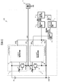
- FIG. 5 shows the overall configuration of the load drive current detection device according to the embodiment of the present invention.
- the load drive current detection device 100 shown in FIG. 5 is configured to generate a gate drive signal HGATE for the high side driver MOS 11 and a low side driver MOS signal in accordance with the PWM signal so that the high side driver MOS 11 and the low side driver MOS 21 are not turned on simultaneously.
- the pre-driver circuit 9 that generates the gate drive signal LGATE of the MOS 21 and the falling edge detection circuit 10 of the PWM signal are detected, the falling edge timing of the PWM signal is detected, and based on the current detection signal DCURL of the current detection circuit 6.
- the enable signal EN that is the output signal of the enable signal generation circuit 7 is used to detect the return current of the low-side driver MOS 21 and the voltage measurement circuit 5 High side current detection circuit 12 by Characterized by stopping the detection of the driving current IoutH of MOS11 for high-side driver based on the output current IcurH.
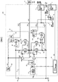
- FIG. 6 as an example in which the embodiment shown in FIG. 5 is applied to a linear solenoid driver, the driver MOS 11 and current detection circuit 12 of the high side driver 1, the driver MOS 12 and current detection circuit 22 of the low side driver 2, and the current Specific block examples or circuit examples of the detection circuit 6, the enable signal generation circuit 7, the pre-driver circuit 9, and the falling edge detection circuit 10 are shown, and the operation is performed using the timing charts in FIGS. explain.
- the linear solenoid driver shown in FIG. 6 includes a power source VB, a VCP booster circuit 126 that outputs a higher potential than the power source VB, an electromagnetic load 4 to be driven connected between the ground GND and the OUT terminal, and a power source VB.
- a high-side driver MOS 11 that is connected between the electromagnetic loads 4 and drives the electromagnetic load 4; a high-side current detection circuit 12 that is connected in parallel with the high-side driver MOS 11 and detects the high-side drive current IoutH; A low-side driver MOS 21 connected between the electromagnetic load 4 and the ground GND to drive the electromagnetic load 4; a low-side current detection circuit 22 connected in parallel with the low-side driver MOS 21 to detect the low-side drive current IoutL; A detection resistor 3 for converting the output current IcurH of the side current detection circuit 12 into a voltage; A low-side precharge circuit that generates a gate voltage HGATE for driving the high-side drive MOS 11 and the detection MOS 121 from the signal PWM and a gate voltage LGATE for driving the low-side drive MOS driver 21 and the detection MOS 221 from the input signal PWM.
- a driver circuit 9 is provided.
- the high-side current detection circuit 12 uses the high-side driver MOS 11, the source terminal, and the gate terminal in common, and the drain terminal uses the drain terminal of the high-side driver MOS 11, the operational amplifier 122, and the MOS 123.
- a high-side current detection MOS 121 connected so as to be equipotential in a negative feedback circuit, and a current copy circuit that outputs the current IcurH proportional to the input to the ground with the drain current IsH of the high-side current detection MOS 121 as an input 124 is provided.
- the low-side current detection circuit 22 is a negative feedback circuit using the source terminal of the low-side driver MOS 21, the operational amplifier 222, and the MOS 223 with the drain terminal and the gate terminal shared with the low-side driver MOS 21.
- a current detection NMOS 221 connected to be equipotential, and a current copy circuit 224 that outputs the current IcurL proportional to the input to the ground with the source current IsL of the low-side current detection MOS 21 as an input.
- the high-side driver MOS 11 and the detection MOS 121 are MOSs on the same silicon substrate, and are preferably arranged in the vicinity, and the ratio of driving current is determined by the ratio of gate width / gate length.
- the high side current detection circuit 12 outputs a current obtained by multiplying the load current IoutH of the high side driver by 1 / ((NH + 1) ⁇ RcH).
- IcurH can have a smaller current value than IoutH.
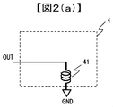
- the electromagnetic load 4 includes, for example, a linear solenoid or inductor 41 connected between the OUT output and the ground GND as shown in FIG.
- a capacitor 42 may be connected between the OUT output and the ground GND.
- the voltage measurement circuit 5 has a function of measuring a voltage value such as an AD converter circuit.
- the voltage measurement circuit 5 operates when the enable signal EN is H and stops when the enable signal EN is L.
- the current detection circuit 6 includes a comparator 61, a resistor 62, and a reference voltage source 63.
- the current detection signal DCURL that is the output signal of the comparator 61 becomes H level when the voltage level is equal to or higher than the voltage level of the reference voltage source 63.
- the enable signal generation circuit 7 includes, for example, a reset priority reset set-flip-flop and RS-FF 71 as shown in FIG.
- the reset priority RS-FF can be composed of an inverter gate 711 and a NAND gate 712.
- the falling edge detection circuit 10 can be composed of, for example, a rising edge trigger type flip-flop 101 of the clock signal CLK, an inverter gate 102, and an AND gate 103 as shown in FIG.
- An H pulse signal can be generated.
- the frequency or duty of the clock signal CLK or a plurality of flip-flops 101 may be connected.
- the reset priority RS-FF 71 shown in FIG. 8 enables the period from L ⁇ H signal change of the DET signal to L ⁇ H of the current detection signal DURL that is the output signal of the current detection circuit 6.
- the signal EN can be set to L level.
- the pre-driver circuit 9 includes a gate drive signal generation circuit 91, a level shift circuit 92, a high-side pre-driver 93H, and a low-side driver 93L.
- the gate drive signal generation circuit 91 In response to the PWM input signal, the gate drive signal generation circuit 91 generates periods TA and TB between the output signal INH0 and the output signal INL as shown in FIG. 7, and the high-side driver MOS 11 and the low-side driver are generated.
- Dead time periods THL and TLH are generated between the gate drive signal HGATE of the high-side driver MOS 11 and the gate drive signal LGATE of the low-side driver MOS 21 so that the MOS MOS 21 does not conduct simultaneously.
- the dead time period is a period in which the gates of the high-side driver MOS 11 and the low-side driver MOS 21 are both turned off and no through current flows.
- FIG. 7 shows an example of a timing chart of the load drive current detection device of the embodiment of FIG.
- the output terminal OUT is switched from the power supply voltage VB to the ON voltage of the high-side driver MOS 11.
- the voltage drops by VonH.
- the VCP voltage supplied to the pre-driver 93H that outputs the HGATE voltage must also be higher than the VB voltage.
- the VCP voltage may be supplied from a device external power supply via a terminal, or may be generated from a VB power supply from a charge pump, a DCDC converter, a bootstrap, or the like.
- the high-side driver MOS 11 When the high-side driver MOS 11 is turned off during the transition from the high-side driver on-period to the high-side driver off-period, a flyback voltage of the electromagnetic load 4 is generated, and the body diode of the low-side driver MOS 21 causes the ground GND to The output current Iout flows. If the influence of the leakage current is ignored at this time, the output terminal OUT becomes a voltage obtained by dropping the forward voltage VOFF of the body diode of the low-side driver MOS 21 from the ground GND. The current flowing at this time is called a return current.
- the return current is detected by the low-side current detection circuit 22 as an IcurH current when the current detection signal DCURL that is the output signal of the current detection circuit 6 changes from L to H.
- a gate drive signal as shown in FIGS.
- the falling edge timing of INH0 that is the output signal of the generation circuit 91 is detected by using the falling edge detection circuit 10.
- the enable signal generating circuit 7 sets the enable signal EN to L as shown in FIG. 7 from the time when the falling edge is detected by the falling edge detection circuit 10 until the return current is detected by the current detection circuit 6.
- the voltage measurement circuit 5 can be stopped during the falling period of the high side driver.
- the power loss PdH of the high-side driver MOS 11 increases locally and transiently during the falling period of the high-side driver, and local and transient heat generation in the high-side driver MOS 11. Will occur.
- the electromagnetic load 4 includes a linear solenoid or inductor 41 connected between the OUT output and the ground GND as shown in FIG. 2A or 2B.
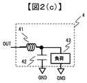
- a non-insulated DC-DC converter configuration in which an inductor 41 and a capacitor 42 are connected to the OUT output may be used.
- the load 43 is supplied by a DC-DC converter.
- a hard disk drive HDD an ASIC (Application Specific Integrated Circuit), an FPGA (Field Programmable Gate Array), an expansion card (PCI CARD).
- Memory DDR memory, DRAM (Dynamic RAM), flash memory, etc.
- CPU Central Processing Unit
- the pre-driver circuit 9 and the falling edge detection circuit 10 shown in FIGS. 5 and 6 are used to start the stop period of the voltage measurement circuit 5 using the enable signal EN.
- the configuration of the load drive current detection device 100 shown in FIG. 1, FIG. 3, or FIG. 4 may be used.
- FIG. 1 shows an overall configuration of a load drive current detection device according to another embodiment of the present invention.
- a load drive current detection device 100 shown in FIG. 1 is electrically connected in parallel with a high-side driver MOS 11 and a high-side driver MOS 11 that cause a drive current Iout to flow through an electromagnetic load 4 such as a solenoid or inductor connected to the ground GND.
- an electromagnetic load 4 such as a solenoid or inductor connected to the ground GND.
- a high-side current detection circuit 12 a low-side driver MOS 21 that causes the drive current Iout to flow through the electromagnetic load 4 and that is electrically connected in series to the high-side driver MOS 11, and an electrical parallel connection to the low-side driver MOS 21
- the low-side current detection circuit 22 the resistor 3 that converts the output current IcurH of the high-side current detection circuit 12 into a voltage value, the voltage measurement circuit 5 for the voltage value converted by the resistor 3, and the output current of the low-side current detection circuit 22 Based on IcurL, the low-side driver MOS 21 Based on the current detection circuit 6 that detects the dynamic current IoutL, and the current detection signal DCURL of the current detection circuit 6, the return current of the low-side driver MOS 21 is detected.
- the enable signal generation circuit 7 The detection of the drive current IoutH of the high-side driver MOS 11 based on the output current IcurH of the high-side current detection circuit 12 by the voltage measurement circuit 5 is stopped using the enable signal EN which is an output signal of
- FIG. 3 shows the overall configuration of a load drive current detection device according to another embodiment of the present invention.
- the load drive current detection device 100 shown in FIG. 3 does not stop the current measurement circuit 5 in response to the enable signal EN, but always operates the current measurement circuit 5, but in response to the current detection result, the enable signal Corresponding to EN, there is provided a current value correction means 8 for correcting in advance the detection error of the high side driver drive current due to local and transient heat generation due to the power loss PdH of the high side driver MOS 11. And
- FIG. 4 shows the overall configuration of a load drive current detection device according to another embodiment of the present invention.
- the dead time period when the high side driver transitions from the on period of the high side driver to the off period of the high side driver in addition to the compatibility of the high side driver EMI reduction and the high accuracy of the current detection function.
- the configuration and operation of a load drive current detection device capable of optimally controlling THL will be described.
- FIG. 11 shows one form of the second embodiment of the present invention, and the difference from FIG. 5 which is one form of Example 1 will be described below. The operation will be described with reference to the timing chart in FIG.
- the load current detection device 100 shown in FIG. 11 can detect the generation of the return current due to the high-side driver being turned off by changing the current detection signal DCURL of the current detection circuit 6 from L ⁇ H. Then, by controlling the pre-driver circuit 9 so as to turn on the gate drive signal LGATE of the low-side driver 2, the dead time period THL can be shortened and optimally controlled.
- this invention is not limited to the above-mentioned Example, Various modifications are included.
- the above-described embodiments have been described in detail for easy understanding of the present invention, and are not necessarily limited to those having all the configurations described.
- a part of the configuration of a certain embodiment can be replaced with the configuration of another embodiment, and the configuration of another embodiment can be added to the configuration of a certain embodiment.
- control lines and signal lines are those that are considered necessary for the explanation, and not all the control lines and signal lines on the product are necessarily shown.
Landscapes
- Electronic Switches (AREA)
Abstract
ハイサイドドライバのEMI低減と電流検出機能の高精度化の両立を可能とする負荷駆動電流検出装置を提供する。 グランドに接続された電磁負荷に駆動電流を流すハイサイドドライバ用MOSと前記ハイサイドドライバ用MOSと電気的に並列に接続したハイサイド電流検出回路と、前記電磁負荷に駆動電流を流し、かつ前記ハイサイドドライバ用MOSと電気的に直列に接続されるローサイドドライバ用MOSと、前記ローサイドドライバ用MOSと電気的に並列に接続したローサイド電流検出回路と、前記ハイサイド電流検出回路の出力電流を電圧値に変換する抵抗と、前記抵抗で変換した電圧値に対する電圧測定回路と、前記ローサイド電流検出回路の出力電流に基づいて前記ローサイドドライバ用MOSの駆動電流を検出する電流検出回路と、前記電流検出回路の電流検出信号に基づいて、前記ローサイドドライバ用MOSの還流電流を検出し、前記還流電流の開始までの期間は、イネーブル信号生成回路の出力信号であるイネーブル信号を用い、前記電圧測定回路による前記ハイサイド電流検出回路の出力電流に基づいた前記ハイサイドドライバ用MOSの駆動電流の検出を停止することを特徴とする負荷駆動電流検出装置。
Description
本発明は、負荷駆動電流検出方式、及びそれを用いた装置に関する。
各種制御対象が電子制御されるに従って、電気信号を機械的運動や油圧に変換するためにモータやソレノイドなどの電動アクチュエータが広く用いられるようになっている。これらの電動アクチュエータを駆動するためには、駆動対象である負荷に流れる電流を高精度に検出する必要がある。
負荷を駆動するドライバ用MOSまたはトランジスタ(以下ではMOSという)に対して並列に小型な電流検出用MOSを接続し、電流検出用MOSに流れる小電流を検出する負荷駆動電流検出装置を提供する方法が用いられている(例えば、特許文献1、特許文献2)。
負荷(例えば、ソレノイド)を駆動するために接続されたドライバ用MOSを例えばPWM(Pulse Width Modulation)制御のために、オンオフして負荷駆動するとき、ドライバ用MOSの出力電圧の高周波成分によるEMI(Electro Magnetic Interference)ノイズが発生する。
十分な負荷駆動電圧波形の立上り時間及び立下り時間(以下では傾きないしはスロープともいう)を持たせ、EMIノイズを低減させる方法は公知である。
従来の負荷駆動電流検出装置の1例として、図13の構成と図14のタイミングチャートを用いて説明する。
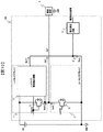
図13に示す負荷駆動電流検出装置100はグランドGNDに接続されたソレノイド、インダクタ等の電磁負荷4に駆動電流Ioutを流すハイサイドドライバ用MOS11とハイサイドドライバ用MOS11と電気的に並列に接続したハイサイド電流検出回路12と、電磁負荷4に駆動電流Ioutを流し、かつハイサイドドライバ用MOS11と電気的に直列に接続されるローサイドドライバ用MOS21と、ハイサイド電流検出回路12の出力電流IcurHを電圧値に変換する抵抗3と、抵抗3で変換した電圧値に対する電圧測定回路5を備える。
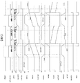
図14に、図13の従来例の負荷駆動電流検出装置のタイミングチャートの一例を示す。
ハイサイドドライバ用MOS11及びハイサイド電流検出回路のゲート駆動信号HGATEと、ローサイドドライバ用MOS21のゲート駆動信号LGATEと、電磁負荷4への出力端子であるOUT端子の電圧と、ハイサイドドライブ用MOS11の出力電流ImHと、ハイサイド電流検出回路12の出力電流IcurHと、ハイサイドドライバ用MOS11のドレイン-ソース間電圧VDSHと、ImH×VDSHで求まるハイサイドドライバ用MOS11の電力損失PdHを図14に示す。
ハイサイドドライバのEMI低減のため、図14に示すように、スロープを持たせることにより、特にハイサイドドライバ立下り時に電力損失PdHが増大する。
ハイサイドドライバ用MOS11とハイサイド電流検出回路12の発熱に対する特性の差異により、電流検出する際に仮定していたハイサイドドライバ駆動電流IoutHとハイサイド電流検出回路の出力電流IcurHとの関係に誤差が発生し、電流検出誤差が発生する。
そこで、本発明は、ハイサイドドライバのEMI低減と電流検出機能の高精度化の両立を可能とする負荷駆動電流検出装置を提供する。
上記課題を解決するために、本発明は、グランドに接続された電磁負荷に駆動電流を流すハイサイドドライバ用MOSと前記ハイサイドドライバ用MOSと電気的に並列に接続したハイサイド電流検出回路と、前記電磁負荷に駆動電流を流し、かつ前記ハイサイドドライバ用MOSと電気的に直列に接続されるローサイドドライバ用MOSと、前記ローサイドドライバ用MOSと電気的に並列に接続したローサイド電流検出回路と、前記ハイサイド電流検出回路の出力電流を電圧値に変換する抵抗と、前記抵抗で変換した電圧値に対する電圧測定回路と、前記ローサイド電流検出回路の出力電流に基づいて前記ローサイドドライバ用MOSの駆動電流を検出する電流検出回路と、前記電流検出回路の電流検出信号に基づいて、前記ローサイドドライバ用MOSの還流電流を検出し、前記還流電流の開始までの期間は、イネーブル信号生成回路の出力信号であるイネーブル信号を用い、前記電圧測定回路による前記ハイサイド電流検出回路の出力電流に基づいた前記ハイサイドドライバ用MOSの駆動電流の検出を停止することを特徴とする負荷駆動電流検出装置を有する。
本発明によれば、ハイサイドドライバのEMI低減と電流検出機能の高精度化の両立を可能とする負荷駆動電流検出装置を提供できる。
上記した以外の課題、構成及び効果は、以下の実施形態の説明により明らかにされる。
以下、図面を参照しつつ、本発明の実施の形態について説明する。なお、図面は簡略的なものであるから、この図面の記載を根拠として本発明の技術的範囲を狭く解釈してはならない。また、同一の要素には、同一の符号を付し、重複する説明は省略する。
本発明の第1の実施形態では、ハイサイドドライバのEMI低減と電流検出機能の高精度化の両立を可能とする負荷駆動電流検出装置の構成及び動作について説明する。
図5は本発明の実施形態である負荷駆動電流検出装置の全体構成である。
図5に示す負荷駆動電流検出装置100は、ハイサイドドライバ用MOS11とローサイドドライバ用MOS21とが同時に導通しないようにPWM信号に応じて、ハイサイドドライバ用MOS11のゲート駆動信号HGATEと、ローサイドドライバ用MOS21のゲート駆動信号LGATEを生成するプリドライバ回路9と、PWM信号の立下りエッジ検出回路10を備え、PWM信号の立下りエッジタイミングを検出し、電流検出回路6の電流検出信号DCURLに基づいて、ローサイドドライバ用MOS21の還流電流を検出し、PWM信号の立下りエッジタイミングから還流電流の開始までの期間には、イネーブル信号生成回路7の出力信号であるイネーブル信号ENを用い、電圧測定回路5によるハイサイド電流検出回路12の出力電流IcurHに基づいたハイサイドドライバ用MOS11の駆動電流IoutHの検出を停止することを特徴とする。
図6では図5に示した実施例をリニアソレノイドドライバに適用した例として、ハイサイドドライバ1のドライバ用MOS11と電流検出回路12と、ローサイドドライバ2のドライバ用MOS12と電流検出回路22と、電流検出回路6と、イネーブル信号生成回路7と、プリドライバ回路9と、立下りエッジ検出回路10の具体的なブロック例または回路例を示し、図7および図10でそのタイミングチャートを用いて動作を説明する。
図6に示すリニアソレノイドドライバは、電源VBと、電源VBより高電位を出力するVCP昇圧回路126と、グランドGNDとOUT端子の間に接続された駆動対象となる電磁負荷4と、電源VBと電磁負荷4の間に接続して電磁負荷4を駆動するハイサイドドライバ用MOS11と、ハイサイドドライバ用MOS11と並列に接続してハイサイドの駆動電流IoutHを検出するハイサイド電流検出回路12と、電磁負荷4とグランドGNDの間に接続して電磁負荷4を駆動するローサイドドライバ用MOS21と、ローサイドドライバ用MOS21と並列に接続してローサイドの駆動電流IoutLを検出するローサイド電流検出回路22と、ハイサイド電流検出回路12の出力電流IcurHを電圧に変換する検出抵抗3と、入力信号PWMからハイサイドドライブ用MOS11と検出用MOS121を駆動するためのゲート電圧HGATEと、入力信号PWMからローサイドドライブ用MOSドラ21と検出用MOS221を駆動するためのゲート電圧LGATEとを生成するローサイドプリドライバ回路9を備えている。
ハイサイド電流検出回路12は例えば、図6に示すように、ハイサイドドライバ用MOS11とソース端子とゲート端子を共通として、ドレイン端子はハイサイドドライバ用MOS11のドレイン端子とオペアンプ122とMOS123を用いた負帰還回路で等電位になるように接続されたハイサイド用電流検出用MOS121と、ハイサイド用電流検出用MOS121のドレイン電流IsHを入力としてグランドに入力に比例した電流IcurHを出力する電流コピー回路124を備えている。電流コピー回路124は例えば、入力電流に対して一定の電流コピー比率RcHとして、出力電流=入力電流/RcH、すなわち、IcurH=IsH/RcHとする。
ローサイド電流検出回路22は例えば、図6に示すように、ローサイドドライバ用MOS21とドレイン端子とゲート端子を共通としてソース端子はローサイドドライバ用MOS21のソース端子とオペアンプ222とMOS223を用いた負帰還回路で等電位になるように接続された電流検出用NMOS221と、ローサイド用電流検出用MOS21のソース電流IsLを入力としてグランドに入力に比例した電流IcurLを出力する電流コピー回路224を備えている。電流コピー回路224として例えば、入力電流に対して一定の電流コピー比率RcLとして、出力電流=入力電流/RcL、すなわち、IcurL=IsL/RcLとする。
ハイサイドドライバ用MOS11と検出用MOS121は同一シリコン基板上のMOSであり、近傍に配置されることが好ましく、ゲート幅/ゲート長の比率で駆動する電流の比率を決定する。例えば、ハイサイドドライバ用MOS11と検出用MOS121のゲート長が同じで、ハイサイドドライバ用MOS11のゲート幅/検出用MOS121のゲート幅=NH(NH>1)としたとき、ハイサイドドライバ用MOS11の駆動電流ImHと検出用MOS121の駆動電流IsHは
ImH=NH×IsH
となり、ハイサイドドライバの出力電流IoutH=IsH+ImHであるので、検出用MOS121の電流IsHは、
IsH=IoutH/(NH+1)
となる。検出用NMOS121の電流IsHは電流コピー比率RcHの電流コピー回路123によりハイサイド電流検出回路12の出力電流IcurHとして出力される。すなわち、
IcurH=IsH/RcH=IoutH/((NH+1)×RcH)
であり、ハイサイド電流検出回路12はハイサイドドライバの負荷電流IoutHを1/((NH+1)×RcH)倍した電流を出力する。ここで、例えば、NH>1かつRcH>1とすることで、IcurHはIoutHに比べ小さな電流値とすることができる。
電磁負荷4は例えば、図2(a)に示すように、OUT出力とグランドGND間に接続されたリニアソレノイドあるいはインダクタ41を備える。もしくは図2(b)に示すように、リニアソレノイドあるいはインダクタ41に加えて、コンデンサ42をOUT出力とグランドGND間に接続された構成でも良い。
電圧測定回路5は例えば、ADコンバータ回路など電圧値を測定する機能を備える。ここで、電圧測定回路5はイネーブル信号ENがHのとき動作し、Lのとき停止することとする。
電流検出回路6は例えば、図6に示すように、コンパレータ61と、抵抗62と、基準電圧源63を備えている。これにより、ローサイド電流検出回路22の出力電流IcurLを抵抗62により、電圧値に変換後、基準電圧源63の電圧レベル以上のとき、コンパレータ61の出力信号である電流検出信号DCURLはHレベルとなる。
電流検出回路6は例えば、図6に示すように、コンパレータ61と、抵抗62と、基準電圧源63を備えている。これにより、ローサイド電流検出回路22の出力電流IcurLを抵抗62により、電圧値に変換後、基準電圧源63の電圧レベル以上のとき、コンパレータ61の出力信号である電流検出信号DCURLはHレベルとなる。
イネーブル信号生成回路7は例えば、図8に示すように、リセット優先リセットセット-フリップフロップ、RS-FF71を備える。ここでリセット優先RS-FFはインバータゲート711と、NANDゲート712で構成できる。
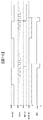
立下りエッジ検出回路10は例えば、図9に示すように、クロック信号CLKの立上りエッジトリガー型のフリップフロップ101と、インバータゲート102と、ANDゲート103で構成できる。図10に示すように、PWM信号に対応した信号であるINH0信号のH→Lの立下りエッジからクロック信号CLKの次ぎの立上りエッジまでの期間、立下りエッジ検出回路10の出力信号DETとして、Hパルス信号を生成できる。このHパルス幅を調整するために例えば、クロック信号CLKの周波数またはデューティーまたはフリップフロップ101を複数個数珠つなぎとしても良い。図8に示したリセット優先RS-FF71により、図10に示すようにDET信号のL→Hの信号変化から電流検出回路6の出力信号である電流検出信号DURLのL→Hまでの期間、イネーブル信号ENをLレベルにすることができる。
プリドライバ回路9は例えば、図6に示すように、ゲート駆動信号発生回路91と、レベルシフト回路92と、ハイサイドプリドライバ93Hと、ローサイドドライバ93Lを備える。PWM入力信号に応じて、ゲート駆動信号生成回路91により、出力信号INH0と出力信号INLとの間に、図7に示すように、期間TA、TBを生成し、ハイサイドドライバ用MOS11とローサイドドライバ用MOS21とが同時に導通しないように、ハイサイドドライバ用MOS11のゲート駆動信号HGATEとローサイドドライバ用MOS21のゲート駆動信号LGATEとの間にデッドタイム期間THLとTLHを生成する。ここでデッドタイム期間とはハイサイドドライバ用MOS11とローサイドドライバ用MOS21のゲートがともにオフし、貫通電流が流れない期間のこととする。
図7に、図6の実施例の負荷駆動電流検出装置のタイミングチャートの一例を示す。
PWM入力信号と、プリドライバ回路9におけるINH0、INH1、INL信号と、ハイサイドドライバ用MOS11及び電流検出用MOS121のゲート駆動信号HGATEと、ローサイドドライバ用MOS21及び電流検出用MOS221のゲート駆動信号LGATEと、電磁負荷4への出力端子であるOUT端子の電圧と、ハイサイドドライブ用MOS11の出力電流ImHと、ハイサイド電流検出回路12の出力電流IcurHと、ハイサイドドライバ用MOS11のドレイン-ソース間電圧VDSHと、ImH×VDSHで求まるハイサイドドライバ用MOS11の電力損失PdHと、ローサイドドライブ用MOS21の出力電流ImLと、ローサイド電流検出回路22の出力電流IcurLと、ローサイドドライブ用MOS21のドレイン-ソース間電圧VDSLと、ImL×VDSLで求まるローサイドドライバ用MOS21の電力損失PdLと、電流検出回路6の出力信号である電流検出信号DCURLと、イネーブル生成回路7の出力信号であるイネーブル信号ENとを図7に示す。
ハイサイドドライバのオン期間は、ハイサイドドライバ用MOS11から電磁負荷4に出力電流Ioutを流すため、リーク電流の影響を無視すると、出力端子OUTは電源電圧VBから、ハイサイドドライバ用MOS11のオン電圧VonH分、電圧降下した電圧となる。ここで、オン電圧VonHはハイサイドドライバ用MOS11のオン抵抗をRonH、駆動電流をImHとした時、VonH=ImH×RonHである。
ハイサイドドライバ用MOS11のソース電圧はOUT端子電圧であるため、MOSの閾値電圧Vthとすると、大電流を駆動するドライバ回路においてオン抵抗RonHは低抵抗であることが好ましく、ImH×RonH<Vthとなる。これより、ハイサイドドライバ用MOS11をオンさせるために必要なHGATEの電圧は、
HGATE電圧=VB-VonH+Vth=VB-ImH×RonH+Vth>VB
となる。よって、HGATE電圧はVB電圧以上であることが必要である。HGATE電圧を出力するプリドライバ93Hに供給するVCP電圧もVB電圧より高電位であることが必要である。
HGATE電圧=VB-VonH+Vth=VB-ImH×RonH+Vth>VB
となる。よって、HGATE電圧はVB電圧以上であることが必要である。HGATE電圧を出力するプリドライバ93Hに供給するVCP電圧もVB電圧より高電位であることが必要である。
VCP電圧は、例えば、装置外部電源から端子経由で供給しても、VB電源からチャージポンプやDCDCコンバータやブートストラップなどから生成して構成してもよい。
ハイサイドドライバのオン期間からハイサイドドライバのオフ期間へ遷移するとき、ハイサイドドライバ用MOS11がオフしたとき、電磁負荷4のフライバック電圧が発生し、ローサイドドライバ用MOS21のボディダイオードによってグランドGNDから出力電流Ioutに流れる。このときリーク電流の影響を無視すると、出力端子OUTはグランドGNDからローサイドドライバ用MOS21のボディダイオードの順方向電圧VOFF電圧降下した電圧となる。このとき流れる電流を還流電流と呼ぶこととする。還流電流はローサイド電流検出回路22により、IcurH電流として、電流検出回路6の出力信号である電流検出信号DCURLがLからHとなることで検出する。
ハイサイドドライバのオン期間からハイサイドドライバのオフ期間への遷移開始の検出方法として、例えば、PWM入力信号の立下りもしくはPWM信号に対応した信号、図6及び図7に示すようなゲート駆動信号生成回路91の出力信号であるINH0の立下りエッジタイミングを立下りエッジ検出回路10を用いて検出する。
立下りエッジ検出回路10により、立下りエッジを検出してから電流検出回路6による還流電流を検出するまでの期間を図7に示すように、イネーブル信号生成回路7により、イネーブル信号ENをLとすることで、ハイサイドドライバの立下り期間、電圧測定回路5を停止することができる。
ソレノイド駆動時のEMI低減のため、ハイサイドドライバの駆動電圧波形OUTに関して、スロープもしくは傾きを持たせることが有効である。しかしながら、図7に示すように、ハイサイドドライバ用MOS11の電力損失PdHはハイサイドドライバの立下り期間に局所的、過渡的に増加し、ハイサイドドライバ用MOS11での局所的、過渡的な発熱が発生する。このため、
IcurH=IsH/RcH=IoutH/((NH+1)×RcH)
の比例関係を前提として、ハイサイドドライバのソレノイド駆動電流IoutHの検出を行うと、ハイサイドドライバの駆動電圧波形OUTの立下り期間はハイサイドドライバ用MOS11と検出用MOS121との発熱に対する特性の差異により、電流検出する際に仮定していたハイサイドドライバ用MOS11の電流ImHと検出用MOS121の電流IsHの以下の関係において、
ImH=NH×IsH
比例係数NHに誤差が発生する。比例係数NHが大きいほど、より大きな電流検出誤差が発生する。
IcurH=IsH/RcH=IoutH/((NH+1)×RcH)
の比例関係を前提として、ハイサイドドライバのソレノイド駆動電流IoutHの検出を行うと、ハイサイドドライバの駆動電圧波形OUTの立下り期間はハイサイドドライバ用MOS11と検出用MOS121との発熱に対する特性の差異により、電流検出する際に仮定していたハイサイドドライバ用MOS11の電流ImHと検出用MOS121の電流IsHの以下の関係において、
ImH=NH×IsH
比例係数NHに誤差が発生する。比例係数NHが大きいほど、より大きな電流検出誤差が発生する。
ハイサイドドライバの立下り期間、イネーブル信号ENにより、電圧測定回路5を停止することにより、ハイサイドドライバの駆動電圧波形OUTの立下り期間におけるハイサイドドライバ用MOS11の電力損失PdHによる局所的、過渡的な発熱によるハイサイドドライバ駆動電流の検出誤差をなくすことができ、電流検出精度を向上することができる。
以上より、ハイサイドドライバのEMI低減と電流検出機能の高精度化の両立できる負荷駆動電流検出装置を可能とする。
以上より、ハイサイドドライバのEMI低減と電流検出機能の高精度化の両立できる負荷駆動電流検出装置を可能とする。
以上では、リニアソレノイドドライバに適用した例として、電磁負荷4として、図2(a)または図2(b)に示すように、OUT出力とグランドGND間に接続されたリニアソレノイドあるいはインダクタ41を備えた場合であったが、図2(c)に示すように、OUT出力にインダクタ41とコンデンサ42が接続した、非絶縁型のDC-DCコンバータ構成でもよい。ここで、負荷43とはDC-DCコンバータが電力を供給する、例えば、ばハードディスクドライブHDD、ASIC(Application Specific Integrated Circuit)、FPGA(Field Programmable Gate Array)、拡張カード(PCI CARD
)、メモリ(DDRメモリ、DRAM(Dynamic RAM)、フラッシュメモリ等)、CPU
(Central Processing Unit)等である。
)、メモリ(DDRメモリ、DRAM(Dynamic RAM)、フラッシュメモリ等)、CPU
(Central Processing Unit)等である。
図5および図6の構成において、イネーブル信号ENを用いた電圧測定回路5の停止期間の開始は図5および図6で示したプリドライバ回路9、立下りエッジ検出回路10を用いたが、これに限定されることなく、以下、図1または図3または図4にて示す負荷駆動電流検出装置100の構成としても良い。
図1は本発明の別実施形態である負荷駆動電流検出装置の全体構成である。
図1に示す負荷駆動電流検出装置100はグランドGNDに接続されたソレノイド、インダクタ等の電磁負荷4に駆動電流Ioutを流すハイサイドドライバ用MOS11とハイサイドドライバ用MOS11と電気的に並列に接続したハイサイド電流検出回路12と、電磁負荷4に駆動電流Ioutを流し、かつハイサイドドライバ用MOS11と電気的に直列に接続されるローサイドドライバ用MOS21と、ローサイドドライバ用MOS21と電気的に並列に接続したローサイド電流検出回路22と、ハイサイド電流検出回路12の出力電流IcurHを電圧値に変換する抵抗3と、抵抗3で変換した電圧値に対する電圧測定回路5と、ローサイド電流検出回路22の出力電流IcurLに基づいてローサイドドライバ用MOS21の駆動電流IoutLを検出する電流検出回路6と、電流検出回路6の電流検出信号DCURLに基づいて、ローサイドドライバ用MOS21の還流電流を検出し、還流電流の開始までの期間は、イネーブル信号生成回路7の出力信号であるイネーブル信号ENを用い、電圧測定回路5によるハイサイド電流検出回路12の出力電流IcurHに基づいたハイサイドドライバ用MOS11の駆動電流IoutHの検出を停止することを特徴とする。
図3は本発明の別実施形態である負荷駆動電流検出装置の全体構成である。
図3に示す負荷駆動電流検出装置100は、イネーブル信号ENに対応して、電流測定回路5を停止させるのではなく、電流測定回路5は常時動作させるがその電流検出結果に対して、イネーブル信号ENに対応して、ハイサイドドライバ用MOS11の電力損失PdHによる局所的、過渡的な発熱によるハイサイドドライバ駆動電流の検出誤差分を予め反映して補正する電流値補正手段8を備えることを特徴とする。
図4は本発明の別実施形態である負荷駆動電流検出装置の全体構成である。
図4に示す負荷駆動電流検出装置100は、ハイサイド電流検出回路12の出力電流IcurHとローサイド電流検出回路22の出力電流IcurL2との和となる和電流Icurを抵抗3により電圧に変換することを特徴とする。
これによりハイサイドドライバの駆動電流だけでなく、ローサイドドライバの駆動電流も電流測定回路5を用いて、検出することが可能となる。
本発明の第2の実施形態では、ハイサイドドライバのEMI低減と電流検出機能の高精度化の両立に加え、ハイサイドドライバのオン期間からハイサイドドライバのオフ期間へ遷移するときのデッドタイム期間THLを最適に制御できる負荷駆動電流検出装置の構成及び動作について説明する。
図11は本発明の第2の実施形態の1形態であり、以下では実施例1の1形態である図5からの差分に関して説明する。図12でそのタイミングチャートを用いて動作を説明する。
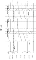
図11に示す負荷電流検出装置100は、図12のタイミングチャートに示すように、ハイサイドドライバ、オフによる還流電流発生は電流検出回路6の電流検出信号DCURLがL→Hとなることで検出でき、その後にローサイドドライバ2のゲート駆動信号LGATEをオンするようにプリドライバ回路9を制御することにより、デッドタイム期間THLを短く、最適に制御することが可能となる。
なお、本発明は上記した実施例に限定されるものではなく、様々な変形例が含まれる。例えば、上記した実施例は本発明を分かりやすく説明するために詳細に説明したものであり、必ずしも説明した全ての構成を備えるものに限定されるものではない。また、ある実施例の構成の一部を他の実施例の構成に置き換える事が可能であり、また、ある実施例の構成に他の実施例の構成を加えることも可能である。また、各実施例の構成の一部について他の構成の追加・削除・置換をする事が可能である。
また、制御線や信号線は説明上必要と考えられるものを示しており、製品上必ずしも全ての制御線や信号線を示しているとは限らない。
1 ハイサイドドライバ
2 ローサイドドライバ
3 抵抗
4 電磁負荷
5 電圧測定回路
6 電流検出回路
7 イネーブル信号生成回路
8 電流値補正手段
9 プリドライバ回路
10 立下りエッジ検出回路
100 負荷駆動電流検出装置
HGATE,LGATE ゲート駆動信号
PWM PWM信号
DCURL 電流検出信号
EN イネーブル信号
DET 立下りエッジ検出信号
CLK クロック信号
VB 電源
GND グランド
2 ローサイドドライバ
3 抵抗
4 電磁負荷
5 電圧測定回路
6 電流検出回路
7 イネーブル信号生成回路
8 電流値補正手段
9 プリドライバ回路
10 立下りエッジ検出回路
100 負荷駆動電流検出装置
HGATE,LGATE ゲート駆動信号
PWM PWM信号
DCURL 電流検出信号
EN イネーブル信号
DET 立下りエッジ検出信号
CLK クロック信号
VB 電源
GND グランド
Claims (10)
- グランドに接続された電磁負荷に駆動電流を流すハイサイドドライバ用MOSと前記ハイサイドドライバ用MOSと電気的に並列に接続したハイサイド電流検出回路と、前記電磁負荷に駆動電流を流し、かつ前記ハイサイドドライバ用MOSと電気的に直列に接続されるローサイドドライバ用MOSと、前記ローサイドドライバ用MOSと電気的に並列に接続したローサイド電流検出回路と、前記ハイサイド電流検出回路の出力電流を電圧値に変換する抵抗と、前記抵抗で変換した電圧値に対する電圧測定回路と、前記ローサイド電流検出回路の出力電流に基づいて前記ローサイドドライバ用MOSの駆動電流を検出する電流検出回路と、前記電流検出回路の電流検出信号に基づいて、前記ローサイドドライバ用MOSの還流電流を検出し、前記還流電流の開始までの期間は、イネーブル信号生成回路の出力信号であるイネーブル信号を用い、前記電圧測定回路による前記ハイサイド電流検出回路の出力電流に基づいた前記ハイサイドドライバ用MOSの駆動電流の検出を停止することを特徴とする負荷駆動電流検出装置。
- 請求項1に記載の負荷駆動電流検出装置において、前記イネーブル信号に応じて、前記電流測定回路の出力信号である電流検出結果に対して、電流値補正手段を適用することを特徴とする負荷駆動電流検出装置。
- 請求項1に記載の負荷駆動電流検出装置において、前記ハイサイドドライバ用MOSと前記ローサイドドライバ用MOSとが同時に導通しないようにPWM信号に応じて、前記ハイサイドドライバ用MOSのゲート駆動信号と、前記ローサイドMOSドライバ用のゲート駆動信号を生成するプリドライバ回路と、前記電流検出信号は、前記プリドライバ回路により生成される前記ゲート駆動信号と、前記ゲート駆動信号とのデッドタイム生成に用いることを特徴とする負荷駆動電流検出装置。
- 請求項2に記載の負荷駆動電流検出装置において、前記ハイサイドドライバ用MOSと前記ローサイドドライバ用MOSとが同時に導通しないようにPWM信号に応じて、前記ハイサイドドライバ用MOSのゲート駆動信号と、前記ローサイドMOSドライバ用のゲート駆動信号を生成するプリドライバ回路と、前記電流検出信号は、前記プリドライバ回路により生成される前記ゲート駆動信号と、前記ゲート駆動信号とのデッドタイム生成に用いることを特徴とする負荷駆動電流検出装置。
- 請求項3に記載の負荷駆動電流検出装置において、前記プリドライバ回路と、前記PWM信号もしくは前記PWM信号に対応した信号の立下りエッジ検出回路を備え、前記PWM信号もしくは前記PWM信号に対応した信号の立下りエッジタイミングを検出し、前記電流検出回路の電流検出信号に基づいて、前記ローサイドドライバ用MOSの還流電流を検出し、前記PWM信号もしくは前記PWM信号に対応した信号の立下りエッジタイミングから前記還流電流の開始までの期間には、イネーブル信号生成回路の出力信号であるイネーブル信号を用い、前記電圧測定回路による前記ハイサイド電流検出回路の出力電流に基づいた前記ハイサイドドライバ用MOSの駆動電流の検出を停止または前記電流検出結果に対して、前記電流値補正手段を適用することを特徴とする負荷駆動電流検出装置。
- 請求項4に記載の負荷駆動電流検出装置において、前記プリドライバ回路と、前記PWM信号もしくは前記PWM信号に対応した信号の立下りエッジ検出回路を備え、前記PWM信号もしくは前記PWM信号に対応した信号の立下りエッジタイミングを検出し、前記電流検出回路の電流検出信号に基づいて、前記ローサイドドライバ用MOSの還流電流を検出し、前記PWM信号もしくは前記PWM信号に対応した信号の立下りエッジタイミングから前記還流電流の開始までの期間には、イネーブル信号生成回路の出力信号であるイネーブル信号を用い、前記電圧測定回路による前記ハイサイド電流検出回路の出力電流に基づいた前記ハイサイドドライバ用MOSの駆動電流の検出を停止または前記電流検出結果に対して、前記電流値補正手段を適用することを特徴とする負荷駆動電流検出装置。
- 請求項1に記載の負荷駆動電流検出装置において、前記ハイサイド電流検出回路の前記出力電流と前記ローサイド電流検出回路の出力電流との和となる和電流を前記抵抗により電圧に変換することを特徴とする負荷駆動電流検出装置。
- 請求項1に記載の負荷駆動電流検出装置であって、前記ハイサイド電流検出回路は前記ハイサイドドライバ用MOSとソース端子とゲート端子を共通として、ドレイン端子は前記ハイサイドドライバ用MOSのドレイン端子とオペアンプを用いた負帰還回路で等電位になるように接続されたハイサイド用電流検出用MOSと、前記ハイサイド用電流検出用MOSのドレイン電流を入力としてグランドに入力に比例した電流を出力する電流コピー回路があり、前記ローサイド電流検出回路は前記ローサイドドライバ用MOSとドレイン端子とゲート端子を共通としてソース端子は前記ローサイドドライバ用MOSのソース端子とオペアンプを用いた負帰還回路で等電位になるように接続された電流検出用MOSと、前記ローサイド用電流検出用MOSのソース電流を入力としてグランドに入力に比例した電流を出力する電流コピー回路であることを特徴とする負荷駆動電流検出装置。
- 請求項1に記載の負荷駆動電流検出装置であって、少なくとも前記ハイサイドドライバ用MOS及び前記ハイサイド電流検出回路の1ないし複数チャネル分を同一のシリコン基板上に形成することを特徴とした半導体集積回路を有する負荷駆動電流検出装置。
- 請求項1に記載の負荷駆動電流検出装置であって、前記電磁負荷として、インダクタから、コンデンサ及び負荷を介して、グランドと接続していることを特徴とする負荷駆動電流検出装置。
Priority Applications (1)
| Application Number | Priority Date | Filing Date | Title |
|---|---|---|---|
| JP2015538952A JP6301942B2 (ja) | 2013-09-25 | 2014-06-16 | 負荷駆動電流検出装置 |
Applications Claiming Priority (2)
| Application Number | Priority Date | Filing Date | Title |
|---|---|---|---|
| JP2013-197677 | 2013-09-25 | ||
| JP2013197677 | 2013-09-25 |
Publications (1)
| Publication Number | Publication Date |
|---|---|
| WO2015045506A1 true WO2015045506A1 (ja) | 2015-04-02 |
Family
ID=52742664
Family Applications (1)
| Application Number | Title | Priority Date | Filing Date |
|---|---|---|---|
| PCT/JP2014/065837 Ceased WO2015045506A1 (ja) | 2013-09-25 | 2014-06-16 | 負荷駆動電流検出装置 |
Country Status (2)
| Country | Link |
|---|---|
| JP (1) | JP6301942B2 (ja) |
| WO (1) | WO2015045506A1 (ja) |
Cited By (1)
| Publication number | Priority date | Publication date | Assignee | Title |
|---|---|---|---|---|
| JP2020191700A (ja) * | 2019-05-20 | 2020-11-26 | ローム株式会社 | 電源制御装置、およびスイッチング電源装置 |
Families Citing this family (1)
| Publication number | Priority date | Publication date | Assignee | Title |
|---|---|---|---|---|
| CN113219233B (zh) * | 2021-04-30 | 2023-06-09 | 石家庄宇飞电子有限公司 | 高边电流采样的电压扩展电路 |
Citations (5)
| Publication number | Priority date | Publication date | Assignee | Title |
|---|---|---|---|---|
| JP2003299363A (ja) * | 2002-04-01 | 2003-10-17 | Nissan Motor Co Ltd | 電流検出機能付き半導体装置 |
| JP2006203415A (ja) * | 2005-01-19 | 2006-08-03 | Toyota Motor Corp | リニアソレノイド駆動回路 |
| JP2010206699A (ja) * | 2009-03-05 | 2010-09-16 | Hitachi Automotive Systems Ltd | ソレノイド電流制御回路 |
| JP2013055620A (ja) * | 2011-09-06 | 2013-03-21 | Hitachi Automotive Systems Ltd | 電流制御装置 |
| JP2014049975A (ja) * | 2012-08-31 | 2014-03-17 | Hitachi Automotive Systems Ltd | 電流検出回路及びそれを用いた電流制御装置 |
-
2014
- 2014-06-16 JP JP2015538952A patent/JP6301942B2/ja not_active Expired - Fee Related
- 2014-06-16 WO PCT/JP2014/065837 patent/WO2015045506A1/ja not_active Ceased
Patent Citations (5)
| Publication number | Priority date | Publication date | Assignee | Title |
|---|---|---|---|---|
| JP2003299363A (ja) * | 2002-04-01 | 2003-10-17 | Nissan Motor Co Ltd | 電流検出機能付き半導体装置 |
| JP2006203415A (ja) * | 2005-01-19 | 2006-08-03 | Toyota Motor Corp | リニアソレノイド駆動回路 |
| JP2010206699A (ja) * | 2009-03-05 | 2010-09-16 | Hitachi Automotive Systems Ltd | ソレノイド電流制御回路 |
| JP2013055620A (ja) * | 2011-09-06 | 2013-03-21 | Hitachi Automotive Systems Ltd | 電流制御装置 |
| JP2014049975A (ja) * | 2012-08-31 | 2014-03-17 | Hitachi Automotive Systems Ltd | 電流検出回路及びそれを用いた電流制御装置 |
Cited By (2)
| Publication number | Priority date | Publication date | Assignee | Title |
|---|---|---|---|---|
| JP2020191700A (ja) * | 2019-05-20 | 2020-11-26 | ローム株式会社 | 電源制御装置、およびスイッチング電源装置 |
| JP7260392B2 (ja) | 2019-05-20 | 2023-04-18 | ローム株式会社 | 電源制御装置、およびスイッチング電源装置 |
Also Published As
| Publication number | Publication date |
|---|---|
| JPWO2015045506A1 (ja) | 2017-03-09 |
| JP6301942B2 (ja) | 2018-03-28 |
Similar Documents
| Publication | Publication Date | Title |
|---|---|---|
| CN102742135B (zh) | 升降压dc-dc转换器以及开关控制电路 | |
| CN103516203B (zh) | 直流对直流控制器与其操作方法 | |
| US7138786B2 (en) | Power supply driver circuit | |
| KR100927882B1 (ko) | Dc-dc 컨버터 및 dc-dc 컨버터의 제어 방법 | |
| TWI458238B (zh) | 直流對直流轉換裝置及其電壓轉換方法 | |
| KR100912865B1 (ko) | 스위칭 레귤레이터 및 그 스위칭 레귤레이터를 구비하는반도체 장치 | |
| US20080278125A1 (en) | Apparatus for optimizing diode conduction time during a deadtime interval | |
| JP4734390B2 (ja) | コンバータの制御回路 | |
| JP5727797B2 (ja) | Dc−dcコンバータ | |
| JP5814892B2 (ja) | 電流検出回路及びそれを用いた電流制御装置 | |
| CN108365742B (zh) | 偏压产生电路及其同步双模式升压直流-直流转换器 | |
| CN108432112B (zh) | Dc-dc变换器以及负载驱动用半导体集成电路 | |
| US9705281B2 (en) | Semiconductor light source driving apparatus | |
| TWI403874B (zh) | 具電流回授之電流控制系統以及電流控制方法 | |
| CN102055336A (zh) | 升压/降压电路 | |
| JP6301942B2 (ja) | 負荷駆動電流検出装置 | |
| US9887625B2 (en) | Output current monitor circuit for switching regulator | |
| US20120313435A1 (en) | Voltage converter | |
| JP7028634B2 (ja) | Dc/dcコンバータの制御回路、制御方法、電源管理回路および電子機器 | |
| JP2011142815A (ja) | コンバータの制御回路 | |
| CN102025273A (zh) | Dc-dc转换器 | |
| JP2017532945A (ja) | 電圧コンバータのためのアダプティブコントローラ | |
| CN104682679A (zh) | 电源转换器及其斜率侦测控制器与方法 | |
| JP5071145B2 (ja) | 制御回路および電源制御用半導体集積回路並びにdc−dcコンバータ | |
| JP2009118692A (ja) | 直流−直流変換装置 |
Legal Events
| Date | Code | Title | Description |
|---|---|---|---|
| 121 | Ep: the epo has been informed by wipo that ep was designated in this application |
Ref document number: 14848738 Country of ref document: EP Kind code of ref document: A1 |
|
| ENP | Entry into the national phase |
Ref document number: 2015538952 Country of ref document: JP Kind code of ref document: A |
|
| NENP | Non-entry into the national phase |
Ref country code: DE |
|
| 122 | Ep: pct application non-entry in european phase |
Ref document number: 14848738 Country of ref document: EP Kind code of ref document: A1 |