WO2015033749A1 - 光電変換素子、色素増感太陽電池および光電変換素子用電子移動促進剤 - Google Patents
光電変換素子、色素増感太陽電池および光電変換素子用電子移動促進剤 Download PDFInfo
- Publication number
- WO2015033749A1 WO2015033749A1 PCT/JP2014/071356 JP2014071356W WO2015033749A1 WO 2015033749 A1 WO2015033749 A1 WO 2015033749A1 JP 2014071356 W JP2014071356 W JP 2014071356W WO 2015033749 A1 WO2015033749 A1 WO 2015033749A1
- Authority
- WO
- WIPO (PCT)
- Prior art keywords
- group
- halogen atom
- photoelectric conversion
- dye
- conversion element
- Prior art date
- Legal status (The legal status is an assumption and is not a legal conclusion. Google has not performed a legal analysis and makes no representation as to the accuracy of the status listed.)
- Ceased
Links
Images

Classifications
-
- H—ELECTRICITY
- H01—ELECTRIC ELEMENTS
- H01G—CAPACITORS; CAPACITORS, RECTIFIERS, DETECTORS, SWITCHING DEVICES, LIGHT-SENSITIVE OR TEMPERATURE-SENSITIVE DEVICES OF THE ELECTROLYTIC TYPE
- H01G9/00—Electrolytic capacitors, rectifiers, detectors, switching devices, light-sensitive or temperature-sensitive devices; Processes of their manufacture
- H01G9/20—Light-sensitive devices
- H01G9/2004—Light-sensitive devices characterised by the electrolyte, e.g. comprising an organic electrolyte
-
- H—ELECTRICITY
- H10—SEMICONDUCTOR DEVICES; ELECTRIC SOLID-STATE DEVICES NOT OTHERWISE PROVIDED FOR
- H10K—ORGANIC ELECTRIC SOLID-STATE DEVICES
- H10K85/00—Organic materials used in the body or electrodes of devices covered by this subclass
- H10K85/60—Organic compounds having low molecular weight
- H10K85/649—Aromatic compounds comprising a hetero atom
- H10K85/654—Aromatic compounds comprising a hetero atom comprising only nitrogen as heteroatom
-
- Y—GENERAL TAGGING OF NEW TECHNOLOGICAL DEVELOPMENTS; GENERAL TAGGING OF CROSS-SECTIONAL TECHNOLOGIES SPANNING OVER SEVERAL SECTIONS OF THE IPC; TECHNICAL SUBJECTS COVERED BY FORMER USPC CROSS-REFERENCE ART COLLECTIONS [XRACs] AND DIGESTS
- Y02—TECHNOLOGIES OR APPLICATIONS FOR MITIGATION OR ADAPTATION AGAINST CLIMATE CHANGE
- Y02E—REDUCTION OF GREENHOUSE GAS [GHG] EMISSIONS, RELATED TO ENERGY GENERATION, TRANSMISSION OR DISTRIBUTION
- Y02E10/00—Energy generation through renewable energy sources
- Y02E10/50—Photovoltaic [PV] energy
- Y02E10/542—Dye sensitized solar cells
-
- Y—GENERAL TAGGING OF NEW TECHNOLOGICAL DEVELOPMENTS; GENERAL TAGGING OF CROSS-SECTIONAL TECHNOLOGIES SPANNING OVER SEVERAL SECTIONS OF THE IPC; TECHNICAL SUBJECTS COVERED BY FORMER USPC CROSS-REFERENCE ART COLLECTIONS [XRACs] AND DIGESTS
- Y02—TECHNOLOGIES OR APPLICATIONS FOR MITIGATION OR ADAPTATION AGAINST CLIMATE CHANGE
- Y02E—REDUCTION OF GREENHOUSE GAS [GHG] EMISSIONS, RELATED TO ENERGY GENERATION, TRANSMISSION OR DISTRIBUTION
- Y02E10/00—Energy generation through renewable energy sources
- Y02E10/50—Photovoltaic [PV] energy
- Y02E10/549—Organic PV cells
Definitions
- the present invention relates to a photoelectric conversion element, a dye-sensitized solar cell, and an electron transfer accelerator for a photoelectric conversion element.
- Photoelectric conversion elements are used in various optical sensors, copiers, solar cells and the like.
- Various types of photoelectric conversion elements have been put to practical use, such as those using metals, semiconductors, organic pigments and dyes, or combinations thereof.
- a solar cell using non-depleting solar energy does not require fuel, and full-scale practical use is highly expected as it uses inexhaustible clean energy.
- silicon-based solar cells have been researched and developed for a long time, and are spreading due to the policy considerations of each country.
- silicon is an inorganic material, there is a limit to improving throughput and cost.
- t-Butylpyridine is useful for improving the photoelectric conversion efficiency in terms of increasing the open-circuit voltage, but on the other hand, it reduces the short-circuit current, thus offsetting the improvement in photoelectric conversion efficiency due to the increase in voltage. A significant improvement in photoelectric conversion efficiency cannot be expected. Therefore, when the electrolyte and its additive used in the dye-sensitized solar cell are examined from the viewpoint of photoelectric conversion efficiency, even if the electrolyte solution described in Patent Documents 1 and 2 or its additive is used, the photoelectric conversion is performed. It was found that the efficiency improvement effect was not sufficient and there was room for improvement.
- This invention makes it a subject to provide the photoelectric conversion element excellent in the photoelectric conversion efficiency, the dye-sensitized solar cell, and the electron transfer promoter for photoelectric conversion elements.
- the present inventors examined the influence of the electrolyte additive on the photoelectric conversion efficiency.
- the substituent of the pyridine compound is important for improving the photoelectric conversion efficiency. I understood.
- the object of the present invention has been achieved by the following means.
- a photoelectric conversion element having, in this order, a photoconductor layer having semiconductor fine particles carrying a dye, a charge transfer layer containing an electrolyte, and a counter electrode on a conductive support,
- the photoelectric conversion element containing the compound represented by following formula (1) between a body and a counter electrode.
- Ac represents an acidic group.
- L represents a single bond or a linking group.
- R is a branched alkyl group, an alkyl group substituted with a halogen atom, a branched alkenyl group, an alkenyl group substituted with a halogen atom, a linear or branched alkynyl group, an alkynyl group substituted with a halogen atom, a halogen atom, a cyano group Or represents a nitro group.
- R 1 and R 2 each independently represents a hydrogen atom or a substituent.
- n1 represents an integer of 0 or more and 3 or less
- n2 and n3 each independently represents an integer of 1 or more and 4 or less.
- R is a branched alkyl group, an alkyl group substituted with a halogen atom, a branched alkenyl group, an alkenyl group substituted with a halogen atom, a linear or branched alkynyl group, or an alkynyl group substituted with a halogen atom ⁇ 1>.
- the photoelectric conversion element as described in 1>.
- ⁇ 3> The photoelectric conversion device according to ⁇ 1> or ⁇ 2>, wherein R is a branched alkyl group.
- R is an alkyl group substituted with a halogen atom, a branched alkenyl group, an alkenyl group substituted with a halogen atom, a linear or branched alkynyl group, or an alkynyl group substituted with a halogen atom ⁇ 1> or ⁇ 1>2>.
- a branched alkyl group, an alkyl group substituted with a halogen atom, a branched alkenyl group, an alkenyl group substituted with a halogen atom, a linear or branched alkynyl group, or an alkynyl group substituted with a halogen atom has 6 to 6 carbon atoms 30.
- ⁇ 6> The photoelectric conversion device according to any one of ⁇ 1> to ⁇ 5>, wherein the halogen atom of the alkyl group, alkenyl group, or alkynyl group substituted with a halogen atom, or the halogen atom of R is a fluorine atom .
- ⁇ 7> The photoelectric conversion device according to any one of ⁇ 1> to ⁇ 6>, wherein the compound represented by the formula (1) has at least one acidic group.
- n1 is an integer of 1 to 3, or at least one of R 1 and R 2 is a substituent having an acidic group.
- ⁇ 9> The photoelectric conversion device according to any one of ⁇ 1> to ⁇ 8>, wherein the acidic group is a carboxy group.
- a dye-sensitized solar cell comprising the photoelectric conversion element according to any one of ⁇ 1> to ⁇ 10>.
- Ac represents an acidic group.
- L represents a single bond or a linking group.
- R is a branched alkyl group, an alkyl group substituted with a halogen atom, a branched alkenyl group, an alkenyl group substituted with a halogen atom, a linear or branched alkynyl group, an alkynyl group substituted with a halogen atom, a halogen atom, a cyano group Or represents a nitro group.
- R 1 and R 2 each independently represents a hydrogen atom or a substituent.
- n1 represents an integer of 0 or more and 3 or less
- n2 and n3 each independently represents an integer of 1 or more and 4 or less.
- the carbon-carbon double bond may be either E-type or Z-type in the molecule, or a mixture thereof.
- substituents, linking groups, etc. hereinafter referred to as substituents, etc.
- Each substituent group may be the same as or different from each other. The same applies to the definition of the number of substituents and the like.
- substituents and the like when a plurality of substituents and the like are close to each other (especially when they are adjacent to each other), they may be connected to each other to form a ring unless otherwise specified.
- a ring such as an alicyclic ring, an aromatic ring, or a hetero ring may be further condensed to form a condensed ring.
- each substituent may be further substituted with a substituent unless otherwise specified.
- the present invention it has become possible to provide a photoelectric conversion element excellent in photoelectric conversion efficiency, a dye-sensitized solar cell, and an electron transfer accelerator for a photoelectric conversion element.
- the photoelectric conversion element of the present invention has, on a conductive support, a photosensitive layer having semiconductor fine particles carrying a dye, a charge transfer layer containing an electrolyte, and a counter electrode (counter electrode) in this order. Between the conductive support and the counter electrode, a compound represented by the following formula (1) (also referred to as the compound of the present invention) is included.
- the compound of the present invention may be present anywhere between the conductive support and the counter electrode, and is preferably contained in at least one of the electrolyte (charge transfer layer) and the surface of the semiconductor fine particles.
- the photoelectric conversion element of this invention has the said structure, another structure will not be specifically limited, The well-known structure regarding a photoelectric conversion element is employable.
- Each layer in the photoelectric conversion element of the present invention may be a single layer or a multilayer, and may have layers other than the above-mentioned layers as necessary.
- the dye-sensitized solar cell of the present invention includes the photoelectric conversion element of the present invention.
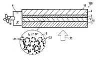
- the photoelectric conversion element or the dye-sensitized solar cell of the present invention can be, for example, an embodiment shown in FIG.
- the photoelectric conversion element 10 includes a conductive support 1, a photoreceptor layer 2 including semiconductor fine particles 22 sensitized by a dye 21, a charge transfer layer 3 that is a hole transport layer, and a counter electrode 4. Consists of.
- the charge transfer body layer 3 contains the compound of the present invention.
- the compound or co-adsorbent of the present invention is adsorbed on the semiconductor fine particles 22 together with the dye 21.
- the conductive support 1 provided with the photoreceptor layer 2 functions as a working electrode in the photoelectric conversion element 10.
- the photoelectric conversion element 10 is shown as a system 100 using a dye-sensitized solar cell that can be used for a battery for causing an operating means (electric motor) M to work with an external circuit 6.
- the light incident on the photoreceptor layer 2 excites the dye 21.
- the excited dye has electrons with high energy, and these electrons are transferred from the dye 21 to the conduction band of the semiconductor fine particles 22 and further reach the conductive support 1 by diffusion.
- the compound of the present invention has a low rearrangement energy, and it is considered that electron transfer from the dye to the semiconductor fine particles is likely to occur.
- the dye 21 is in an oxidant due to the above-described electron transfer, the electron on the electrode works in the external circuit 6 and passes through the counter electrode 4 and the charge transfer body layer 3 in which the electrolyte is present, thereby the dye 21. By returning to the photoreceptor layer 2 where the oxidant is present, it functions as a solar cell.
- the material used for the photoelectric conversion element or the dye-sensitized solar cell and the method for producing each member may be the usual ones of this type, for example, US Pat. No. 4,927,721.
- U.S. Pat.No. 4,684,537, U.S. Pat.No. 5,0843,65, U.S. Pat.No. 5,350,644, U.S. Pat.No. 5,463,057 Reference can be made to US Pat. No. 5,525,440, JP-A-7-249790, JP-A-2004-220974, and JP-A-2008-135197.
- the outline of the compound of the present invention and the main member will be described.
- the photoelectric conversion element of this invention contains the compound represented by following formula (1).
- Ac represents an acidic group.
- L represents a single bond or a linking group.
- R is a branched alkyl group, an alkyl group substituted with a halogen atom, a branched alkenyl group, an alkenyl group substituted with a halogen atom, a linear or branched alkynyl group, an alkynyl group substituted with a halogen atom, a halogen atom, a cyano group Or represents a nitro group (hereinafter also referred to as “specific substituent R”).
- R 1 and R 2 each independently represents a hydrogen atom or a substituent.
- n1 represents an integer of 0 or more and 3 or less
- n2 and n3 each independently represents an integer of 1 or more and 4 or less.
- the compound of the present invention has an amino group NR 1 R 2 and a specific substituent R, and preferably has a group “Ac-L” containing an acidic group Ac.
- the compound of the present invention having the specific substituent R together with the amino group NR 1 R 2 is preferably contained in at least the electrolyte or adsorbed on the surface of the semiconductor fine particles. Thereby, photoelectric conversion efficiency can be improved.
- T-Butylpyridine which has been widely used conventionally, is adsorbed on the surface of semiconductor fine particles and recombines the semiconductor fine particles, that is, electrons transferred to the photoreceptor layer and oxide ions (for example, I 3 ⁇ ) of a redox pair. Is suppressed, and a voltage drop of the photoelectric conversion element is prevented. Further, the voltage is improved by reducing the Fermi level of the semiconductor fine particles due to the effect of the electron donating group. On the other hand, since the conduction band becomes shallow at the same time, the energy difference from the lowest empty orbital (LUMO) level of the dye is reduced. It is considered that this makes it difficult for electrons to move smoothly from the dye to the semiconductor fine particles, and the current of the photoelectric conversion element decreases.
- LUMO lowest empty orbital
- the compound of the present invention has the following effects in addition to the effect of preventing the voltage drop.
- amino groups can also exist more in the vicinity of the dye by functioning as adsorbing groups for the semiconductor fine particles.
- the rearrangement energy of the surrounding solvent molecules with respect to the change in the dye charge during the electron transfer from the photoexcitation of the dye to the semiconductor fine particles can be reduced. Thereby, the energy barrier at the time of electron movement is made small, and electron movement easily occurs. That is, the rearrangement energy is low and the electron transfer of the dye is likely to occur, thereby increasing the current.
- the compound of the present invention further has an acidic group Ac, it is adsorbed on the surface of the semiconductor fine particles, the reverse electron transfer of electrons is effectively suppressed, and the photoelectric conversion efficiency is further increased.
- the specific substituent R may be any of the above groups, but from the viewpoint of photoelectric conversion efficiency, a branched alkyl group, an alkyl group substituted with a halogen atom, a branched alkenyl group, a halogen atom
- a branched alkyl group substituted with a linear or branched alkynyl group and an alkynyl group substituted with a halogen atom are preferred.
- the specific substituent R is preferably an alkyl group substituted by a halogen atom, a branched alkenyl group, an alkenyl group substituted by a halogen atom, a straight chain, A branched alkynyl group or an alkynyl group substituted with a halogen atom, more preferably an alkyl group substituted with a halogen atom.
- the specific substituent R is more preferably a branched alkyl group in that it is excellent in the effect of improving the photoelectric conversion efficiency by increasing the voltage.
- the branched alkyl group of the specific substituent R is not particularly limited as long as it is a branched alkyl group, but it is excellent in the effect of improving the photoelectric conversion efficiency and also has excellent solubility in an organic solvent or the like.
- the number of carbon atoms is preferably 6 to 30, more preferably 7 to 27, and still more preferably 10 to 25.
- Examples of the branched alkyl group include i-propyl, t-butyl, i-butyl, 4-methylpentyl, 2-ethylhexyl, 3-ethylheptyl, 3-decylpentadecyl and the like.
- the alkyl group substituted with a halogen atom is not particularly limited as long as at least one hydrogen atom bonded to the carbon atom constituting the alkyl group is substituted with a halogen atom. It may be a branched alkyl group.
- the alkyl group substituted with a halogen atom preferably has 6 to 30 carbon atoms, more preferably 7 to 27, and still more preferably 10 to 25, like the branched alkyl group.
- the halogen atom substituted with a hydrogen atom is not particularly limited, and examples thereof include a fluorine atom, a chlorine atom, a bromine atom, and an iodine atom, and a fluorine atom is preferable in that the effect of improving photoelectric conversion efficiency is excellent.
- the number of hydrogen atoms substituted with halogen atoms and the bonding position of the halogen atoms are not particularly limited, and both are appropriately set.
- the bonding position of the halogen atom is preferably the terminal of the alkyl group.
- Examples of the linear alkyl group substituted with a halogen atom include trifluoromethyl, 6,6,6,5,5,4,4,3,3-nonafluoro-1-hexyl, and the like.
- Examples of the branched alkyl group substituted with a halogen atom include 2-fluoro-2-propyl.
- the branched alkenyl group is not particularly limited as long as it is a branched alkenyl group, but like the branched alkyl group, it preferably has 6 to 30 carbon atoms, more preferably 7 to 27 carbon atoms, and further preferably 10 to 25 carbon atoms.
- Examples of the branched alkenyl group include 2-methyl-1-propenyl.
- the alkenyl group substituted with a halogen atom is not particularly limited as long as at least one hydrogen atom bonded to the carbon atom constituting the alkenyl group is substituted with a halogen atom. It may be a branched alkenyl group.
- the alkenyl group substituted with a halogen atom preferably has 6 to 30 carbon atoms, more preferably 7 to 27, and still more preferably 10 to 25, like the branched alkyl group.
- the halogen atom substituted with the hydrogen atom is the same as the halogen atom of the alkyl group substituted with the halogen atom.
- the number of hydrogen atoms substituted with halogen atoms and the bonding position of halogen atoms are not particularly limited, and both are appropriately set.
- the bonding position of the halogen atom is preferably the terminal of the alkenyl group. Examples of the alkenyl group substituted with a halogen atom include 1,2,2-trifluorovinyl.
- the straight chain or branched alkynyl group is not particularly limited, but like the branched alkyl group, it preferably has 6 to 30 carbon atoms, more preferably 7 to 27, and still more preferably 10 to 25.
- Examples of the linear alkynyl group include ethynyl and butynyl, and examples of the branched alkynyl group include 3,3-dimethylbutynyl.
- the alkynyl group substituted with a halogen atom is not particularly limited as long as at least one hydrogen atom bonded to the carbon atom constituting the alkynyl group is substituted with a halogen atom, and may be a linear alkynyl group. It may be a branched alkynyl group.
- the alkynyl group substituted with a halogen atom preferably has 6 to 30 carbon atoms, more preferably 7 to 27 carbon atoms, and still more preferably 10 to 25 carbon atoms, like the branched alkyl group.
- the halogen atom substituted with the hydrogen atom is the same as the halogen atom of the alkyl group substituted with the halogen atom.
- the number of hydrogen atoms substituted with halogen atoms and the bonding position of halogen atoms are not particularly limited, and both are appropriately set.
- the bonding position of the halogen atom is preferably the terminal of the alkynyl group.
- Examples of the alkynyl group substituted with a halogen atom include 3,3,3-trifluoropropynyl and the like.
- halogen atom examples include a fluorine atom, a chlorine atom, a bromine atom, and an iodine atom, and a fluorine atom and a chlorine atom are preferable and a fluorine atom is more preferable in that the effect of improving the photoelectric conversion efficiency is excellent.
- R 1 and R 2 each independently represents a hydrogen atom or a substituent.
- the amide group, the substituent W mentioned later, and the substituent which has an acidic group are mentioned.
- the substituent having an acidic group may be any substituent having an acidic group Ac described later, such as an acidic group Ac described later, a group represented by “Ac-L” described later, and a substituent W described later. Among them, a substituent having an acidic group, a substituent W substituted with an acidic group Ac, and the like can be given.
- R 1 and R 2 are each preferably a substituent having a hydrogen atom, an amide group, an alkyl group or an acidic group.
- Ac is an acidic group, and specifically, any adsorbing group that adsorbs to the surface of the semiconductor fine particles may be used.
- the acidic group is preferably a group having a dissociative proton, and specifically, one having a pKa of 11 or less is preferable.
- the acidic group Ac may take the form of releasing a proton and dissociating, or may be a salt.
- the acidic group Ac is preferably a carboxy group (—CO 2 H), —SO 3 H, —PO 3 H 2 , —OH, —SH or a salt thereof, more preferably —CO 2 H, —OH or a salt thereof.
- L represents a single bond or a linking group.
- the linking group may be a divalent group that connects the pyridine ring and the acidic group Ac, and examples thereof include a divalent group of the substituent W described later.
- an alkylene group, an ethenylene group, an ethynylene group, an arylene group, a heteroaromatic ring group, and a group obtained by combining these are preferable.
- L is preferably a single bond or an alkylene group.
- the linking group represented by L may have a substituent, and examples of the substituent include the substituent W described later.
- the compound of the present invention may have a substituent in addition to the above-described specific substituent R, amino group NR 1 R 2 and “Ac-L”.
- substituents are not particularly limited.
- a group other than the group represented by the specific substituent R, the amino group NR 1 R 2 and “Ac-L” Is mentioned.
- One or more other substituents may be present.
- Other substituents may be bonded to a group represented by the specific substituent R, amino group NR 1 R 2 or “Ac-L” to form a ring together with these, and there are a plurality of other substituents. Sometimes, they may combine with each other to form a ring.
- n1 represents an integer of 0 or more and 3 or less, preferably an integer of 1 or more and 3 or less, and more preferably 1 or 2.
- n2 represents an integer of 1 or more and 4 or less, preferably an integer of 1 or more and 3 or less, and more preferably 1 or 2.
- n3 represents an integer of 1 or more and 4 or less, preferably an integer of 1 or more and 3 or less, and more preferably 1 or 2.
- n1, n2 and n3 are appropriately set, and the total of n1, n2 and n3 is an integer of 2 or more and 5 or less.
- the compound of the present invention preferably has at least one acidic group in terms of adsorptivity to the surface of the semiconductor fine particles. Therefore, in formula (1), the types of R 1 and R 2 in the amino group NR 1 R 2 are selected such that there is at least one acidic group, or n1 and n2 are selected from the above ranges Is done. For example, it is preferable that n1 is an integer of 1 to 3, or at least one of R 1 and R 2 is a substituent having an acidic group, and n2 is an integer of 1 to 3.
- the specific substituent R, the amino group NR 1 R 2 and the group represented by “Ac-L” may be bonded to any carbon atom constituting the pyridine ring.
- the bonding position of the amino group NR 1 R 2 and the group represented by “Ac-L” is preferably the 2-position or the 6-position of the pyridine ring from the viewpoint of adsorptivity to the surface of the semiconductor fine particle, and the amino group NR 1 R 2 is more preferably 2-position, and the group represented by “Ac-L” is more preferably 6-position.
- the binding position of the specific substituent R is the binding position of the amino group NR 1 R 2 in that recombination with an oxidant ion and recombination with a dye can be suppressed, and the approach of a solvent to the periphery of the dye is suppressed.
- the 4-position, the 4-position or 5-position of the pyridine ring is preferred.
- a substituent that does not specify substitution / non-substitution means that the group may have an arbitrary substituent. This is also synonymous for compounds that do not specify substitution / non-substitution.
- Preferred substituents include the following substituent W.
- substituent W when a substituent is simply described, the following substituent W is referred to.
- substituent W examples include the following.
- An alkyl group preferably having 1 to 20 carbon atoms, such as methyl, ethyl, isopropyl, t-butyl, pentyl, heptyl, 1-ethylpentyl, benzyl, 2-ethoxyethyl, 1-carboxymethyl, trifluoromethyl, etc.
- Alkenyl groups preferably having 2 to 20 carbon atoms, such as vinyl, allyl, oleyl, etc.
- alkynyl groups preferably having 2 to 20 carbon atoms, such as ethynyl, butynyl, phenylethynyl, etc.
- cycloalkyl groups preferably Has 3 to 20 carbon atoms, for example, cyclopropyl, cyclopentyl, cyclohexyl, 4-methylcyclohexyl and the like, cycloalkenyl group (preferably having 5 to 20 carbon atoms
- alkoxycarbonyl group preferably having 2 to 20 carbon atoms such as ethoxycarbonyl, 2-ethylhexyloxycarbonyl, etc.
- a cycloalkoxycarbonyl group preferably having 4 to 20 carbon atoms such as cyclopropyloxycarbonyl, cyclopentyloxycarbonyl, etc.
- Cyclohexyloxycarbonyl, etc. aryloxycarbonyl groups (preferably having 6 to 20 carbon atoms, such as phenyloxycarbonyl, naphthyloxycarbonyl, etc.)
- amino groups preferably having 0 to 20 carbon atoms, alkylamino groups, alkenyls
- An acyl group preferably having 1 to 20 carbon atoms such as acetyl, cyclohexylcarbonyl, benzoyl, etc.
- an acyloxy group preferably having 1 to 20 carbon atoms such as acetyloxy, cyclohexylcarbonyloxy).
- Benzoyloxy, etc. carbamoyl group (preferably an carbamoyl group having 1 to 20 carbon atoms, alkyl, cycloalkyl or aryl, such as N, N-dimethylcarbamoyl, N-cyclohexylcarbamoyl, N-phenylcarbamoyl, etc.)
- N, N-dimethylcarbamoyl, N-cyclohexylcarbamoyl, N-phenylcarbamoyl, etc.
- An acylamino group (preferably an acylamino group having 1 to 20 carbon atoms, such as acetylamino, cyclohexylcarbonylamino, benzoylamino, etc.), a sulfonamide group (preferably an alkyl, cycloalkyl or aryl sulfonamide having 0 to 20 carbon atoms) Groups such as methanesulfonamide, benzenesulfonamide, N-methylmethanesulfonamide, N-cyclohexylsulfonamide, N-ethylbenzenesulfonamide, etc., alkylthio groups (preferably having 1 to 20 carbon atoms, eg, methylthio , Ethylthio, isopropylthio, benzylthio, etc.), cycloalkylthio groups (preferably having 3 to 20 carbon atoms, such as cyclopropylthio, cyclopent
- a silyl group (preferably a silyl group having 1 to 20 carbon atoms and substituted by alkyl, aryl, alkoxy and aryloxy, such as triethylsilyl, triphenylsilyl, diethylbenzylsilyl, dimethylphenylsilyl, etc.), silyloxy group ( Preferably, it is a silyloxy group having 1 to 20 carbon atoms and substituted with alkyl, aryl, alkoxy and aryloxy, such as triethylsilyloxy, triphenylsilyloxy, diethylbenzylsilyloxy, dimethylphenylsilyloxy, etc.), hydroxyl group , Cyano group, nitro group, halogen atom (for example, fluorine atom, chlorine atom, bromine atom, iodine atom), carboxy group, sulfo group, phosphonyl group, phosphoryl group, boric acid group, more
- the compound or the substituent includes an alkyl group, an alkenyl group, etc.
- these may be linear or branched, and may be substituted or unsubstituted.
- an aryl group, a heterocyclic group and the like may be monocyclic or condensed, and may be substituted or unsubstituted.
- the compound of the present invention may be a commercially available product or may be synthesized.
- the compound of this invention is compoundable according to a well-known method etc. according to a substituent using a commercially available pyridine compound.
- a branched alkyl group can be introduced by using a strong base and an alkylating agent for a pyridine skeleton having a methyl group as a substituent.
- the halogen-substituted alkyl group can be obtained by reacting an OH group in the alkyl group with a halogenating agent in addition to the same method as the branched alkyl group.
- An alkenyl group can be introduced, for example, by carrying out a Bittig reaction on a pyridine skeleton having a formyl group as a substituent.
- the alkynylene group can be introduced by performing Sonogashira reaction or the like on a pyridine skeleton having a halogen group.
- the synthesis method is not limited to these.
- the conductive support is preferably a support made of glass or plastic having a conductive film layer on the surface, such as a metal, which is conductive in itself.
- the plastic support include a transparent polymer film described in paragraph No. 0153 of JP-A No. 2001-291534.
- the support in addition to glass and plastic, ceramic (Japanese Patent Laid-Open No. 2005-135902) or conductive resin (Japanese Patent Laid-Open No. 2001-160425) may be used.
- the surface may be provided with a light management function. For example, an antireflection film in which high refractive films and low refractive index oxide films described in JP-A-2003-123859 are alternately laminated And a light guide function described in JP-A-2002-260746.
- the thickness of the conductive film layer is preferably 0.01 to 30 ⁇ m, more preferably 0.03 to 25 ⁇ m, and particularly preferably 0.05 to 20 ⁇ m.
- the conductive support is substantially transparent.
- substantially transparent means that the transmittance of light (wavelength 300 to 1200 nm) is 10% or more, preferably 50% or more, particularly preferably 80% or more.
- a glass or plastic coated with a conductive metal oxide is preferable.
- the metal oxide tin oxide (TO) is preferable, and fluorine-doped oxide such as indium-tin oxide (tin-doped indium oxide; ITO) and fluorine-doped tin oxide (FTO) is particularly preferable.
- the coating amount of the conductive metal oxide at this time is preferably 0.1 to 100 g per 1 m 2 of the glass or plastic support. When a transparent conductive support is used, light is preferably incident from the support side.
- the photoreceptor layer is designed according to the purpose and has semiconductor fine particles carrying a dye.
- the dye 21 in the photoreceptor layer 2 may be a single type or a mixture of various types.
- the photoreceptor layer preferably has semiconductor fine particles on which at least one of the compound of the present invention and the coadsorbent is supported together with a dye.
- the light receiving electrode 5 includes the conductive support 1 and the photoreceptor layer 2.
- the semiconductor fine particles are preferably metal chalcogenides (for example, oxides, sulfides, selenides, etc.) or perovskite semiconductor fine particles.
- metal chalcogenides for example, oxides, sulfides, selenides, etc.
- perovskite semiconductor fine particles Preferred examples of the metal chalcogenide include titanium, tin, zinc, tungsten, zirconium, hafnium, strontium, indium, cerium, yttrium, lanthanum, vanadium, niobium, tantalum oxide, cadmium sulfide, cadmium selenide, and the like.
- Preferred perovskites include strontium titanate and calcium titanate. Of these, titanium oxide (titania), zinc oxide, tin oxide, and tungsten oxide are particularly preferable.
- titania examples include anatase type, brookite type, and rutile type, and anatase type and brookite type are preferable. Titania nanotubes, nanowires, and nanorods may be mixed with titania semiconductor fine particles or used as semiconductor electrodes.
- the particle diameters of the semiconductor fine particles are 0.001 to 1 ⁇ m as primary particles and 0.01 to 100 ⁇ m as the average particle diameter of the dispersion as the average particle diameter using the diameter when the projected area is converted into a circle. preferable.
- a method of coating the semiconductor fine particles on the conductive support there are a dry method and other methods in addition to a wet method.
- the semiconductor fine particles preferably have a large surface area so as to adsorb many dyes and, if desired, the compound of the present invention. For example, in a state where the semiconductor fine particles are coated on the support, the surface area is preferably 10 times or more, more preferably 100 times or more the projected area.
- the thickness of the semiconductor fine particle layer which is a semiconductor fine particle layer (semiconductor layer) varies depending on the use of the photoelectric conversion element, but is typically 0.1 to 100 ⁇ m. When used as a dye-sensitized solar cell, the thickness is preferably 1 to 50 ⁇ m, more preferably 3 to 30 ⁇ m.
- the semiconductor fine particles are preferably subjected to a baking treatment in order to adhere the particles to each other after being applied to the support.
- the firing conditions can be, for example, 100 to 800 ° C. and 10 minutes to 10 hours.
- the film forming temperature of the semiconductor fine particle layer is not particularly limited. For example, if the conductive support is glass, the film is preferably formed at 60 to 400 ° C.
- the coating amount of semiconductor fine particles per 1 m 2 of support is preferably 0.5 to 500 g, more preferably 5 to 100 g.
- a dye is used.
- dye can use a normal thing in a photoelectric conversion element and a dye-sensitized solar cell, without being specifically limited.
- Such dyes include Ru metal complex dyes, squarylium cyanine dyes, organic dyes, porphyrin dyes, and phthalocyanine dyes.
- the organic dye is preferably a cyanine dye.
- the Ru metal complex dye is preferably a dye represented by the following formula (DA), preferably a Ru metal complex dye coordinated with a ligand of a bipyridine or terpyridine skeleton, and an Ru metal complex having an amino group in the molecule. Dyes are also preferred.
- L1 represents a monodentate ligand
- L2 represents a bidentate ligand
- L3 represents a tridentate ligand
- CI represents a counter ion when a counter ion is required to neutralize the charge.
- m1 represents an integer of 0 to 3
- m2 represents an integer of 0 to 3
- m3 represents an integer of 0 to 2.
- m1 + m2 ⁇ 2 + m3 ⁇ 3 6.
- the monodentate ligand in L1 is preferably a halogen ion, a cyanate anion, an isocyanate anion, a thiocyanate anion, an isothiocyanate anion, a selenocyanate anion, or an isoselenocyanate anion, and more preferably an isocyanate anion, an isothiocyanate anion, or an isoselenocyanate anion.
- an isothiocyanate anion is particularly preferred.
- bipyridine especially 2,2′-bipyridine
- 1,3-diketone are preferred, bipyridine is more preferred, and bipyridine substituted with a carboxy group (particularly 4,4′-diketone).
- Carboxy-2,2′-bipyridine) is more preferred.
- the tridentate ligand in L3 is preferably a ligand in which three nitrogen-containing heteroaryl rings are bonded by a single bond between ring-constituting carbon atoms bonded to the ring-constituting nitrogen atom of the nitrogen-containing heteroaryl ring.
- the nitrogen-containing heteroaryl ring the hetero atom constituting the ring is preferably a nitrogen atom, an oxygen atom, or a sulfur atom, and the number of ring members is preferably a 5-membered ring or 6-membered ring, and the ring is an aromatic ring, It may be condensed with an aliphatic ring or a heterocyclic ring.
- Examples of the 5-membered ring constituting the nitrogen-containing heteroaryl group include pyrrole ring, imidazole ring, pyrazole ring, oxazole ring, thiazole ring, triazole ring, furan ring, thiophene ring, benzimidazole ring, benzoxazole ring, and benzothiazole. Ring, indoline ring, and indazole ring.
- Examples of the 6-membered ring include a pyridine ring, a pyrimidine ring, a pyrazine ring, a triazine ring, a quinoline ring, and a quinazoline ring.
- L3 is particularly preferably terpyridine (particularly 2,2 ′: 6 ′, 2 ′′ -terpyridine).
- These nitrogen-containing heteroaryl rings are preferably those having a carboxy group substituted, more preferably two or more nitrogen-containing heteroaryl rings having a carboxy group substituted, and three nitrogen-containing heteroaryl rings having a carboxy group substituted. More preferred. Of these, 4,4 ′, 4 ′′ -tricarboxy-2,2 ′: 6 ′, 2 ′′ -terpyridine is preferable.
- CI includes Cl ⁇ , I ⁇ , CF 3 SO 3 ⁇ (TfO ⁇ ), PF 6 ⁇ , H + , N (C 4 H 9 ) 4 + (NBu 4 + ), and Cl ⁇ , N (C 4 H 9 ) 4 + is preferred.
- Ru metal complex dyes examples include Ru metal complex dyes described in JP-A-7-500630 (in particular, Examples 1 to 5 on page 5, lower left column, line 5 to page 7, upper right column, line 7).
- the dye synthesized in Example 19 Ru metal complex dye described in JP-T-2002-512729 (especially synthesized in Examples 1 to 16 from the third line to the 29th line and the 23rd line from the bottom of page 20) Dyes), Ru metal complex dyes described in JP-A No. 2001-59062 (particularly dyes described in paragraph Nos. 0087 to 0104), Ru metal complex dyes described in JP-A No. 2001-6760 (particularly, paragraphs) Dyes described in JP-A Nos.
- Ru metal complex dyes described in JP-A No. 2001-253894 particularly, dyes described in paragraph Nos. 0009 to 0010), and R described in JP-A No. 2003-212851 Metal complex dyes (especially the dyes described in paragraph 0005), Ru metal complex dyes described in WO 2007/91525 pamphlet (particularly the dyes described in [0067]), JP-A-2001-291534 Ru metal complex dyes described in the above (especially dyes described in paragraphs 0120 to 0144), Ru metal complex dyes described in JP2012-012570A (in particular, dyes described in paragraphs 0095 to 0103), JP Ru metal complex dyes described in JP 2013-084594 A (particularly dyes described in paragraphs 0072 to 0081), Ru metal complex dyes described in WO 2013/088888 (especially [0286] to [0 [0293].
- Ru metal complex dye examples include butyl group.
- Ru represents a butyl group.
- some Os metal complex dyes other than Ru are also exemplified, but after Ru metal complex dyes, preferred metal complex dyes.
- squarylium cyanine dyes described in JP-A No. 11-214730 particularly dyes described in paragraphs 0036 to 0047
- squarylium cyanine dyes described in JP-A No. 2012-144688 in particular, And dyes described in paragraph numbers 0039 to 0046 and paragraph numbers 0054 to 0060
- squarylium cyanine dyes described in JP 2012-84503 A in particular, dyes described in paragraph numbers 0066 to 0076 and the like.
- organic dyes described in JP-A No. 2004-063274 particularly dyes described in paragraph Nos. 0017 to 0021
- organic dyes described in JP-A No. 2005-123033 particularly paragraph numbers.
- porphyrin dyes examples include Angew. Chem. Int. Ed. , 49, 1-5 (2010), and the like.
- phthalocyanine dye for example, Angew. Chem. Int. Ed. , 46, 8358 (2007), and the like.
- a plurality of dyes may be used in combination.
- the dye used in combination include the aforementioned Ru metal complex dye, squarylium cyanine dye, or organic dye.
- the total amount of the dye used is preferably 0.01 to 100 mmol, more preferably 0.1 to 50 mmol, and particularly preferably 0.1 to 10 mmol per 1 m 2 of the support.
- the dye used in the present invention is preferably one that functions alone as a sensitizing dye of a dye-sensitized solar cell.
- the adsorption amount of the dye to the semiconductor fine particles is preferably 0.001 to 1 mmol, more preferably 0.1 to 0.5 mmol, with respect to 1 g of the semiconductor fine particles. By using such a dye amount, the sensitizing effect in the semiconductor fine particles can be sufficiently obtained.
- the counter ion is not particularly limited, and includes, for example, an alkali metal ion or a quaternary ammonium ion in addition to the CI.
- the adsorption of the dye to the semiconductor fine particles is preferably performed using a dye solution containing the dye, as will be described later.
- a semiconductor electrode in which a semiconductor fine particle layer (photoreceptor layer) is formed on a support can be performed by immersing it in a dye solution obtained by dissolving a dye.
- the compound of the present invention is preferably used and contained in the electrolyte or adsorbed on the surface of the semiconductor fine particles together with the dye.
- the compound of the present invention is preferably contained in at least one of the photosensitive layer, the surface of the photosensitive layer, the charge transfer layer, and the surface of the charge transfer layer.
- a plurality of the compounds of the present invention may be used in combination.
- the compound of this invention is as having mentioned above as a compound represented by Formula (1).
- the compound of the present invention is adsorbed on the semiconductor fine particles
- the compound of the present invention can be adsorbed on the surface of the semiconductor fine particles.
- the surface treatment liquid and the surface treatment method of the semiconductor fine particles will be described later.
- a coadsorbent and adsorb it on the surface of the semiconductor fine particles together with the dye.
- a co-adsorbent a co-adsorbent having at least one acidic group (preferably a carboxy group or a salt group thereof) is preferable, and examples thereof include compounds having a fatty acid or a steroid skeleton.
- the fatty acid may be a saturated fatty acid or an unsaturated fatty acid, and examples thereof include butanoic acid, hexanoic acid, octanoic acid, decanoic acid, hexadecanoic acid, dodecanoic acid, palmitic acid, stearic acid, oleic acid, linoleic acid, and linolenic acid.
- Examples of the compound having a steroid skeleton include cholic acid, glycocholic acid, chenodeoxycholic acid, hyocholic acid, deoxycholic acid, lithocholic acid, ursodeoxycholic acid and the like.
- cholic acid deoxycholic acid and chenodeoxycholic acid
- more preferred are chenodeoxycholic acid Preferred are cholic acid, deoxycholic acid and chenodeoxycholic acid, and more preferred are chenodeoxycholic acid.
- the compound described in paragraph No. 0107 of JP2012-012570A is preferred, and the description of paragraph No. 0107 in JP2012-012570A is preferably incorporated in the present specification as it is.
- the co-adsorbent has an effect of suppressing inefficient association of the dye by adsorbing to the semiconductor fine particles and an effect of preventing reverse electron transfer from the surface of the semiconductor fine particles to the redox system in the electrolyte.
- the amount of coadsorbent used is not particularly limited, but it is preferably 1 to 200 mol, more preferably 10 to 150 mol, and particularly preferably 20 to 50 mol with respect to 1 mol of the dye. It is preferable from the viewpoint of being expressed.
- the charge transfer layer used in the photoelectric conversion element of the present invention is provided between the light receiving electrode and the counter electrode.
- the charge transfer layer is a layer having a function of replenishing electrons to the dye oxidant.
- the charge transfer layer has an electrolyte.
- the charge transfer layer is made of an electrolyte.
- the electrolyte include a liquid electrolyte obtained by dissolving a redox couple in an organic solvent, a so-called gel electrolyte obtained by impregnating a polymer matrix obtained by dissolving a redox couple in an organic solvent, and a molten salt containing the redox couple. .
- a liquid electrolyte is preferred for increasing efficiency.
- iodine and iodide iodide salt, ionic liquid is preferable, lithium iodide, tetrabutylammonium iodide, tetrapropylammonium iodide, methylpropylimidazolium iodide are preferable
- alkyl viologens for example, methyl viologen chloride, hexyl viologen bromide, benzyl viologen tetrafluoroborate
- polyhydroxybenzenes for example, hydroquinone, naphthohydroquinone, etc.
- divalent And trivalent iron complexes for example, red blood salt and yellow blood salt
- divalent and trivalent cobalt complexes and the like.
- a combination of iodine and iodide is preferable, and a combination of divalent and trivalent cobalt complexes is preferable, and a combination of iodine and iodide is particularly preferable.
- the cobalt complex is preferably a complex represented by the formula (A) described in paragraphs 0060 to 0063 of JP2013-077449A, and described in paragraphs 0060 to 0077 of JP2013-077749A. Are preferably incorporated in the present specification as they are.
- iodine and iodide When a combination of iodine and iodide is used as the electrolyte, it is preferable to further use an iodine salt of a 5-membered or 6-membered nitrogen-containing aromatic cation.
- the electrolyte preferably has the compound of the present invention in addition to the redox couple.
- the compounds of the present invention are as described above.
- a pyridine compound other than the compound of the present invention a benzimidazole compound, an imidazole compound, a urea derivative, an amide compound, a pyrimidine compound, and a nitrogen-free heterocyclic ring may be added. it can.
- the organic solvent that dissolves the redox couple, the compound of the present invention that is suitably contained, and the additive that is optionally contained, is not particularly limited, but an aprotic polar solvent (for example, acetonitrile, propylene carbonate, carbonic acid, etc.). Ethylene, dimethylformamide, dimethyl sulfoxide, sulfolane, 1,3-dimethylimidazolinone, 3-methyloxazolidinone and the like are preferable.
- the organic solvent of the liquid electrolyte is a nitrile compound, an ether compound, an ester compound or the like, preferably a nitrile compound, and particularly preferably acetonitrile or methoxypropionitrile.
- Examples of the polymer (polymer matrix) used in the gel electrolyte matrix include polyacrylonitrile and polyvinylidene fluoride.
- Examples of the molten salt include those imparted with fluidity at room temperature by mixing polyethylene oxide with lithium iodide and at least one other lithium salt (such as lithium acetate and lithium perchlorate). . In this case, the amount of the polymer added is 1 to 50% by mass.
- ⁇ -butyrolactone may be included in the electrolytic solution, thereby increasing the diffusion efficiency of iodide ions and improving the photoelectric conversion efficiency.
- a method of controlling the moisture of the electrolytic solution may be taken.
- Preferred methods for controlling moisture include a method for controlling the concentration and a method in which a dehydrating agent is allowed to coexist.
- an inclusion compound of iodine and cyclodextrin may be used, and conversely, a method of constantly supplying water may be used.
- Cyclic amidine may be used, and an antioxidant, hydrolysis inhibitor, decomposition inhibitor, and zinc iodide may be added.
- a molten salt may be used as the electrolyte, and preferred molten salts include ionic liquids containing imidazolium or triazolium type cations, oxazolium-based, pyridinium-based, guanidinium-based, and combinations thereof. These cationic systems may be combined with specific anions. Additives may be added to these molten salts. You may have a liquid crystalline substituent. Further, a quaternary ammonium salt-based molten salt may be used.
- lithium iodide and at least one other lithium salt are mixed with polyethylene oxide to provide fluidity at room temperature. Etc.
- the electrolyte may be quasi-solidified by adding a gelling agent to an electrolyte solution composed of an electrolyte and a solvent to cause gelation (hereinafter, the quasi-solid electrolyte is also referred to as “pseudo-solid electrolyte”).
- the gelling agent include organic compounds having a molecular weight of 1000 or less, Si-containing compounds having a molecular weight in the range of 500 to 5000, organic salts made of a specific acidic compound and a basic compound, sorbitol derivatives, and polyvinylpyridine.
- a method of confining the matrix polymer, the crosslinkable polymer compound or monomer, the crosslinking agent, the electrolyte, and the solvent in the polymer may be used.
- a matrix polymer a polymer having a nitrogen-containing heterocyclic ring in the main chain or side chain repeating unit, a crosslinked product obtained by reacting these with an electrophilic compound, a polymer having a triazine structure, or having a ureido structure Inclusion of polymers, liquid crystal compounds, ether-bonded polymers, polyvinylidene fluoride, methacrylate / acrylate, thermosetting resins, crosslinked polysiloxane, polyvinyl alcohol (PVA), polyalkylene glycol and dextrin Examples thereof include compounds, systems to which oxygen-containing or sulfur-containing polymers are added, natural polymers, and the like.
- the matrix polymer a system including a cross-linked polymer obtained by reacting a bifunctional or higher functional isocyanate with a functional group such as a hydroxyl group, an amino group, or a carboxy group may be used.
- a crosslinking method in which a crosslinked polymer composed of a hydrosilyl group and a double bond compound, polysulfonic acid, polycarboxylic acid, or the like is reacted with a divalent or higher valent metal ion compound may be used.
- Examples of the solvent that can be preferably used in combination with the quasi-solid electrolyte include a specific phosphate ester, a mixed solvent containing ethylene carbonate, and a solvent having a specific dielectric constant.
- the liquid electrolyte solution may be held in a solid electrolyte membrane or pores, and preferred methods thereof include conductive polymer membranes, fibrous solids, and cloth solids such as filters.
- a solid charge transport layer such as a p-type semiconductor or a hole transport material, for example, CuI, CuNCS, or the like can be used. Also, Nature, vol. 486, p. The electrolyte described in 487, 2012, or the like may be used. An organic hole transport material may be used as the solid charge transport layer.
- the organic hole transport material is preferably a conductive polymer such as polythiophene, polyaniline, polypyrrole or polysilane, and a spiro compound in which two rings share a central element such as C or Si and a tetrahedral structure, an aromatic such as triarylamine Group amine derivatives, triphenylene derivatives, nitrogen-containing heterocyclic derivatives, and liquid crystalline cyano derivatives.
- a conductive polymer such as polythiophene, polyaniline, polypyrrole or polysilane
- a spiro compound in which two rings share a central element such as C or Si and a tetrahedral structure, an aromatic such as triarylamine Group amine derivatives, triphenylene derivatives, nitrogen-containing heterocyclic derivatives, and liquid crystalline cyano derivatives.
- the redox couple becomes an electron carrier, it preferably contains a certain concentration.
- a preferable concentration is 0.01 mol / L or more in total, more preferably 0.1 mol / L or more, and particularly preferably 0.3 mol / L or more.
- the upper limit in this case is not particularly limited, but is usually about 5 mol / L.
- the compound of this invention exhibits the function, it is preferable to contain in a certain amount of density
- a preferred concentration is 0.01 mol / L or more, more preferably 0.1 mol / L or more, and particularly preferably 0.25 mol / L or more.
- the upper limit in this case is not particularly limited, but is usually about 5 mol / L.
- the counter electrode is preferably a positive electrode of a dye-sensitized solar cell (photoelectrochemical cell).
- the counter electrode is usually synonymous with the conductive support described above, but the support is not necessarily required in a configuration in which the strength is sufficiently maintained.
- As the structure of the counter electrode a structure having a high current collecting effect is preferable.
- at least one of the conductive support and the counter electrode described above must be substantially transparent.
- the conductive support is preferably transparent, and sunlight is preferably incident from the support side. In this case, it is more preferable that the counter electrode has a property of reflecting light.
- a counter electrode of the dye-sensitized solar cell glass or plastic on which metal or conductive oxide is vapor-deposited is preferable, and glass on which platinum is vapor-deposited is particularly preferable.
- the dye-sensitized solar cell it is preferable to seal the side surface of the battery with a polymer, an adhesive or the like in order to prevent the constituents from evaporating.
- the present invention is disclosed in Japanese Patent No. 4260494, Japanese Patent Application Laid-Open No. 2004-146425, Japanese Patent Application Laid-Open No. 2000-340269, Japanese Patent Application Laid-Open No. 2002-289274, Japanese Patent Application Laid-Open No. 2004-152613, and Japanese Patent Application Laid-Open No. 9-27352. It can apply to the described photoelectric conversion element and a dye-sensitized solar cell.
- Electron transfer accelerator for photoelectric conversion element is a compound represented by the formula (1), and when used in a photoelectric conversion element, the effect of preventing voltage drop and the electron transfer of a dye as described above. Demonstrate the effect of promoting.
- the electron transfer accelerator for a photoelectric conversion element of the present invention is added to an electrolyte composition for a photoelectric conversion element, or a semiconductor fine particle of a photoelectric conversion element or a surface treatment solution for a photoreceptor layer to produce, for example, a photoelectric conversion element. Used to.
- Electrolyte composition and surface treatment liquid are preferably produced by using at least one of an electrolyte composition and a semiconductor fine particle or a surface treatment solution for a photoreceptor layer.
- the electrolyte composition and the surface treatment liquid preferably contain the compound of the present invention as an additive, more preferably as an electron transfer accelerator for a photoelectric conversion element.
- the compounds of the present invention are as described above.
- the electrolyte composition is a material that becomes an electrolyte of a photoelectric conversion element.
- the electrolyte composition may contain any of the liquid electrolyte, the gel electrolyte, and the molten salt as an electrolyte, but a liquid electrolyte is preferable.
- the components, organic solvents, and contents of these electrolytes are as described above. Adjustment of the water content of the electrolyte composition in the photoelectric conversion element or the dye-sensitized solar cell is preferable for effectively achieving the effects of the present invention. For example, the water content (content) of the electrolyte composition is set to 0. It is more preferable to adjust to 0.1 mass%.
- This electrolyte composition is provided between the photoreceptor layer and the counter electrode in the production of the photoelectric conversion element. For example, a liquid electrolyte can be injected or introduced between the photoreceptor layer and the counter electrode.
- the surface treatment liquid only needs to contain the compound of the present invention, and is usually a composition containing a solvent. Although it does not specifically limit as a solvent, The same thing as what was illustrated by the said electrolyte can be mentioned.
- examples of other components that the surface treatment liquid may contain include the additives and coadsorbents.
- the concentration of the compound of the present invention in the surface treatment liquid is not particularly limited, but is preferably 0.01 to 1.0 mol / L, and more preferably 0.05 to 0.5 mol / L, for example.
- This surface treatment liquid is applied to semiconductor fine particles or a photoreceptor layer or used as an immersion liquid in the production of a photoelectric conversion element. Specific examples include a method of immersing a substrate having semiconductor fine particles adsorbed with a dye in an acetonitrile solution containing the compound of the present invention at a concentration of 0.05 mol / L for 30 minutes.
- ⁇ Method for Producing Dye-Sensitized Solar Cell it is preferable to provide a charge transfer body layer using the electrolyte composition containing the compound of this invention.
- the method for providing the charge transfer layer using the electrolyte composition is not particularly limited, and in the case of a liquid electrolyte, the above method can be used.
- the method for surface-treating the semiconductor fine particles or the photoreceptor layer using the surface treatment liquid is as described above.
- a dye adsorption electrode it is preferable to produce a dye adsorption electrode using a dye solution containing a dye.
- the dye is dissolved in a solvent, and may contain a co-adsorbent and other components as necessary.
- the solvent to be used include the solvents described in JP-A-2001-291534, but are not particularly limited.
- an organic solvent is preferable, and alcohols, amides, nitriles, hydrocarbons, and a mixed solvent of two or more of these are preferable.
- the mixed solvent a mixed solvent of an alcohol and a solvent selected from amides, nitriles or hydrocarbons is preferable.
- alcohols and amides are further preferred.
- mixed solvents of alcohols and hydrocarbons are particularly preferred.
- mixed solvents of alcohols and amides are preferable. Specifically, methanol, ethanol, propanol, butanol, dimethylformamide, and dimethylacetamide are preferable.
- the dye solution preferably contains a co-adsorbent.
- the dye solution is preferably one in which the concentration of the dye or co-adsorbent is adjusted so that the solution can be used as it is when producing a photoelectric conversion element or a dye-sensitized solar cell.
- the pigment is preferably contained in an amount of 0.001 to 0.1% by mass.
- the water content of the dye solution is particularly preferably adjusted. Therefore, in the present invention, the water content (content ratio) is particularly preferably adjusted to 0 to 0.1% by mass.
- a semiconductor electrode for a dye-sensitized solar cell in which a dye is supported on the surface of semiconductor fine particles provided in the semiconductor electrode using the dye solution is preferable. Moreover, it is preferable to manufacture a dye-sensitized solar cell by supporting a dye on the surface of semiconductor fine particles provided in the semiconductor electrode using the dye solution.
- Example 1 Preparation of dye-sensitized solar cell> A dye-sensitized solar cell was prepared as described below, and the photoelectric conversion efficiency was measured.
- T1 to T5 T7 to T13, T21 and T22 were used.
- those not commercially available were synthesized according to the following synthesis method of compounds T11 and 22.
- N749 Black Dye
- a photoelectrode having the same configuration as that of the photoelectrode 12 shown in FIG. 5 described in JP-A-2002-289274 is prepared by the following procedure, and further replaced with the photoelectrode in FIG.
- a 10 ⁇ 10 mm scale dye-sensitized solar cell 20 having the same configuration as that of the dye-sensitized solar cell 20 of FIG. 3 was prepared except that the lever photoelectrode was used.
- the specific configuration is shown in FIG. In FIG.
- 41 is a transparent electrode
- 42 is a semiconductor electrode
- 43 is a transparent conductive film
- 44 is a substrate
- 45 is a semiconductor layer
- 46 is a light scattering layer
- 40 is a photoelectrode
- 20 is a dye-sensitized solar cell
- CE is The counter electrode
- E is an electrolyte
- S is a spacer.
- Paste A A titania slurry was prepared by placing spherical TiO 2 particles (anatase, average particle size; 25 nm, hereinafter referred to as spherical TiO 2 particles A) in a nitric acid solution and stirring. Next, a cellulosic binder was added to the titania slurry as a thickener and kneaded to prepare paste A.
- a titania slurry was prepared by stirring spherical TiO 2 particles A and spherical TiO 2 particles (anatase, average particle size: 200 nm, hereinafter referred to as spherical TiO 2 particles B) in a nitric acid solution. .
- rod-like TiO 2 particles C anatase, diameter: 100 nm, aspect ratio: 5, hereinafter referred to as rod-like TiO 2 particles C
- a transparent electrode 41 (conductive support) in which a fluorine-doped SnO 2 conductive film 43 (transparent conductive film 43, film thickness: 500 nm) was formed on a glass substrate 44 (substrate 44) was prepared. Then, the SnO 2 conductive film, a paste 1 of the above screen printing and then dried. Then, it baked on the conditions of 450 degreeC in the air. Further, by repeating this screen printing and baking using the paste 2, a semiconductor electrode having the same configuration as the semiconductor electrode 42 shown in FIG. 2 (light-receiving surface area; 10 mm ⁇ 10 mm, layer) is formed on the SnO 2 conductive film.
- a photoelectrode containing no dye was prepared.
- the dye (N749) was adsorbed to the photoelectrode prepared as described above.
- N, N-dimethylformamide / t-BuOH 1/1 is used as a solvent, and a dye is dissolved in the solvent at a concentration of 3 ⁇ 10 ⁇ 4 mol / L.
- chenodeoxychol is used as a coadsorbent.
- 20 mol of an equimolar mixture of acid and cholic acid was added to 1 mol of the dye to prepare a dye solution.
- the water content of this dye solution was measured by Karl Fischer titration and found to be less than 0.01% by mass.
- the semiconductor electrode prepared above was immersed in this solution, thereby completing the photoelectrode 40 in which the dye was adsorbed to the semiconductor electrode 42 by about 1.5 ⁇ 10 ⁇ 7 mol / cm 2 .
- a platinum electrode thinness of Pt thin film; 100 nm having the same shape and size as the above-mentioned photoelectrode 40 as the counter electrode CE, and 1,2-dimethyl-3-propylimidazolium iodide (as the electrolyte E) 0.6M), iodine (0.1M) and lithium iodide (0.1M), and the compound of the present invention or the comparative compound (concentration 0.30 mol / L) dissolved in acetonitrile to prepare an electrolyte A composition (liquid electrolyte) was prepared. When the water content of this electrolyte composition was measured by Karl Fischer titration, it was less than 0.01% by mass.
- a DuPont spacer S (trade name: “Surlin”) having a shape corresponding to the size of the semiconductor electrode 42 is prepared, as shown in FIG. 3 described in JP-A-2002-289274. Then, the photoelectrode 40, the counter electrode CE, and the spacer S were opposed to each other, and the inside was filled with the electrolyte composition to form an electrolyte E, thereby completing a dye-sensitized solar cell using the photoelectrode 40.
- the battery characteristic test was performed by irradiating 1000 W / m 2 of pseudo-sunlight from a xenon lamp through an AM1.5 filter using a solar simulator (manufactured by WACOM, WXS-85H). The current-voltage characteristics were measured using an IV tester to determine the photoelectric conversion efficiency. The measured short-circuit current JSC and open circuit voltage V OC , and the obtained photoelectric conversion efficiency were evaluated based on the following criteria for the following comparative compound TA.
- Comparative compound TA is t-butylpyridine (TBP, Comparative Example 2 described in Patent Document 2) used conventionally, and Comparative Compound TB is Compound No. 1 described in Patent Document 1. 18.
- the dye-sensitized solar cell of the present invention including the compounds of the present invention (Samples No.1 ⁇ 13) are short-circuit current J SC increases, is excellent in photoelectric conversion efficiency I understood it.
- the short-circuit current J SC is further increased, It was found that the photoelectric conversion efficiency was excellent.
- the dye-sensitized solar cell including a compound having a branched alkyl group as specified substituent R with an amino group NR 1 R 2 is, open voltage V OC be increased in addition to the short-circuit current J SC, better photoelectric conversion It turns out that efficiency is demonstrated.
- certain substituents R If it is 6 or more radicals carbons, increased open circuit voltage V OC is large in addition to the short-circuit current J SC, significant improvement in the photoelectric conversion efficiency was observed.
- the dye-sensitized solar cell including the compound having the acidic group Ac in addition to the specific substituent R and the amino group NR 1 R 2 is particularly excellent in that the short circuit current JSC and the open circuit voltage V OC are greatly increased. It was found that the photoelectric conversion efficiency was exhibited.
- a comparative dye-sensitized solar cell (sample No. c1) containing the comparative compound TA having only t-butyl and a comparative example containing the comparative compound TB having an amino group and two methyl groups dye-sensitized solar cell (sample No.C2) has a smaller short-circuit current J SC and the open circuit voltage V OC, photoelectric conversion efficiency was small.
- the short-circuit current JSC is particularly small, and excellent photoelectric properties are obtained. It was confirmed that conversion efficiency could not be obtained.
- Comparative Compound TA and Comparative Compound TB do not have sufficient adsorptive power with respect to semiconductor fine particles, cannot lower the rearrangement energy, and cannot improve the electron transfer efficiency.
Landscapes
- Engineering & Computer Science (AREA)
- Chemical & Material Sciences (AREA)
- Power Engineering (AREA)
- Chemical Kinetics & Catalysis (AREA)
- Electrochemistry (AREA)
- Microelectronics & Electronic Packaging (AREA)
- Physics & Mathematics (AREA)
- Spectroscopy & Molecular Physics (AREA)
- Materials Engineering (AREA)
- Hybrid Cells (AREA)
- Photovoltaic Devices (AREA)
Abstract
光電変換素子用電子移動促進剤は、下記式(1)で表される。光電変換素子は、導電性支持体上に、色素が担持された半導体微粒子を有する感光体層と、電解質を含む電荷移動体層と、対極とをこの順で有する光電変換素子であって、前記導電性支持体および前記対極の間に下記式(1)で表される化合物を含む。色素増感太陽電池は、この光電変換素子を具備する。 式中、Acは酸性基を表す。Lは単結合または連結基を表す。Rは、分岐アルキル基、ハロゲン原子で置換されたアルキル基、分岐アルケニル基、ハロゲン原子で置換されたアルケニル基、直鎖もしくは分岐アルキニル基、ハロゲン原子で置換されたアルキニル基、ハロゲン原子、シアノ基またはニトロ基を表す。R1およびR2は各々独立に水素原子または置換基を表す。n1は0以上3以下の整数を表し、n2およびn3は各々独立に1以上4以下の整数を表す。
Description
本発明は、光電変換素子、色素増感太陽電池および光電変換素子用電子移動促進剤に関する。
光電変換素子は各種の光センサー、複写機、太陽電池等に用いられている。この光電変換素子には金属を用いたもの、半導体を用いたもの、有機顔料や色素を用いたもの、あるいはこれらを組み合わせたものなどの様々な方式が実用化されている。特に、非枯渇性の太陽エネルギーを利用した太陽電池は、燃料が不要であり、無尽蔵のクリーンエネルギーを利用するものとして、その本格的な実用化が大いに期待されている。その中でも、シリコン系太陽電池は古くから研究開発が進められ、各国の政策的な配慮もあって普及が進んでいる。しかし、シリコンは無機材料であり、スループットおよびコスト等の改良には自ずと限界がある。
そこで色素増感太陽電池の研究が精力的に行われている。特にその契機となったのは、スイス ローザンヌ工科大学のGraetzel等の研究成果である。彼らは、ポーラス酸化チタン薄膜の表面にルテニウム錯体からなる色素を固定した構造を採用し、アモルファスシリコン並の光電変換効率を実現した。これにより、高価な真空装置を使用しなくても製造できる色素増感太陽電池が一躍世界の研究者から注目を集めるようになった。
色素増感太陽電池に使用される色素は積極的に研究され、これまでに、N3、N719、N749、Z907、J2と呼ばれる色素(増感色素ともいう)等が開発されている。
一方、色素増感太陽電池に使用される電解質の添加剤については、従来、t-ブチルピリジンが多用されており、色素に比べると研究、報告例は多くない。例えば、特許文献1および2が挙げられる。
一方、色素増感太陽電池に使用される電解質の添加剤については、従来、t-ブチルピリジンが多用されており、色素に比べると研究、報告例は多くない。例えば、特許文献1および2が挙げられる。
t-ブチルピリジンは、開放電圧を増大させる点で光電変換効率の向上に有用であるが、その一方で短絡電流を減少させることから、電圧増大による光電変換効率の向上を相殺してしまい、大幅な光電変換効率の向上は見込めない。そこで、色素増感太陽電池に使用される電解質およびその添加剤などについて、光電変換効率の観点から検討したところ、特許文献1および2に記載の電解質溶液またはその添加剤であっても、光電変換効率の向上効果が十分ではなく、改善の余地があることがわかった。
本発明は、光電変換効率に優れた光電変換素子、色素増感太陽電池、および、光電変換素子用電子移動促進剤を提供することを、課題とする。
本発明は、光電変換効率に優れた光電変換素子、色素増感太陽電池、および、光電変換素子用電子移動促進剤を提供することを、課題とする。
本発明者らは、電解質の添加剤が光電変換効率に与える影響を検討したところ、電解質の添加剤としてピリジン化合物を用いる場合にピリジン化合物が有する置換基が光電変換効率の向上に重要であることがわかった。しかも、ピリジン環に特定置換基とアミノ基とを組み合わせて導入すると、従来の添加剤に比べて光電変換効率を向上できることを見出した。これらの知見に基づき、アミノ基と特定置換基との組み合わせについてさらに検討を進めた結果、本発明に至った。
すなわち、本発明の課題は、以下の手段によって達成された。
<1>導電性支持体上に、色素が担持された半導体微粒子を有する感光体層と、電解質を含む電荷移動体層と、対極とをこの順で有する光電変換素子であって、導電性支持体および対極の間に下記式(1)で表される化合物を含む光電変換素子。

式中、Acは酸性基を表す。Lは単結合または連結基を表す。Rは、分岐アルキル基、ハロゲン原子で置換されたアルキル基、分岐アルケニル基、ハロゲン原子で置換されたアルケニル基、直鎖もしくは分岐アルキニル基、ハロゲン原子で置換されたアルキニル基、ハロゲン原子、シアノ基またはニトロ基を表す。R1およびR2は各々独立に水素原子または置換基を表す。n1は0以上3以下の整数を表し、n2およびn3は各々独立に1以上4以下の整数を表す。
<2>Rが、分岐アルキル基、ハロゲン原子で置換されたアルキル基、分岐アルケニル基、ハロゲン原子で置換されたアルケニル基、直鎖もしくは分岐アルキニル基またはハロゲン原子で置換されたアルキニル基である<1>に記載の光電変換素子。
<3>Rが、分岐アルキル基である<1>または<2>に記載の光電変換素子。
<4>Rが、ハロゲン原子で置換されたアルキル基、分岐アルケニル基、ハロゲン原子で置換されたアルケニル基、直鎖もしくは分岐アルキニル基またはハロゲン原子で置換されたアルキニル基である<1>または<2>に記載の光電変換素子。
<5>分岐アルキル基、ハロゲン原子で置換されたアルキル基、分岐アルケニル基、ハロゲン原子で置換されたアルケニル基、直鎖もしくは分岐アルキニル基またはハロゲン原子で置換されたアルキニル基の炭素数が6~30である<1>~<4>のいずれかに記載の光電変換素子。
<6>ハロゲン原子で置換された、アルキル基、アルケニル基もしくはアルキニル基のハロゲン原子、または、Rのハロゲン原子が、フッ素原子である<1>~<5>のいずれかに記載の光電変換素子。
<7>式(1)で表される化合物が、少なくとも1つの酸性基を有する<1>~<6>のいずれかに記載の光電変換素子。
<8>n1が1以上3以下の整数であるか、または、R1およびR2の少なくとも一方が酸性基を有する置換基である<7>に記載の光電変換素子。
<9>酸性基が、カルボキシ基である<1>~<8>のいずれかに記載の光電変換素子。
<10>式(1)で表される化合物が、電解質中、および、半導体微粒子の表面の少なくとも一方に含まれる<1>~<9>のいずれかに記載の光電変換素子。
<11><1>~<10>のいずれかに記載の光電変換素子を具備する色素増感太陽電池。
<3>Rが、分岐アルキル基である<1>または<2>に記載の光電変換素子。
<4>Rが、ハロゲン原子で置換されたアルキル基、分岐アルケニル基、ハロゲン原子で置換されたアルケニル基、直鎖もしくは分岐アルキニル基またはハロゲン原子で置換されたアルキニル基である<1>または<2>に記載の光電変換素子。
<5>分岐アルキル基、ハロゲン原子で置換されたアルキル基、分岐アルケニル基、ハロゲン原子で置換されたアルケニル基、直鎖もしくは分岐アルキニル基またはハロゲン原子で置換されたアルキニル基の炭素数が6~30である<1>~<4>のいずれかに記載の光電変換素子。
<6>ハロゲン原子で置換された、アルキル基、アルケニル基もしくはアルキニル基のハロゲン原子、または、Rのハロゲン原子が、フッ素原子である<1>~<5>のいずれかに記載の光電変換素子。
<7>式(1)で表される化合物が、少なくとも1つの酸性基を有する<1>~<6>のいずれかに記載の光電変換素子。
<8>n1が1以上3以下の整数であるか、または、R1およびR2の少なくとも一方が酸性基を有する置換基である<7>に記載の光電変換素子。
<9>酸性基が、カルボキシ基である<1>~<8>のいずれかに記載の光電変換素子。
<10>式(1)で表される化合物が、電解質中、および、半導体微粒子の表面の少なくとも一方に含まれる<1>~<9>のいずれかに記載の光電変換素子。
<11><1>~<10>のいずれかに記載の光電変換素子を具備する色素増感太陽電池。
<12>下記式(1)で表される光電変換素子用電子移動促進剤。

式中、Acは酸性基を表す。Lは単結合または連結基を表す。Rは、分岐アルキル基、ハロゲン原子で置換されたアルキル基、分岐アルケニル基、ハロゲン原子で置換されたアルケニル基、直鎖もしくは分岐アルキニル基、ハロゲン原子で置換されたアルキニル基、ハロゲン原子、シアノ基またはニトロ基を表す。R1およびR2は各々独立に水素原子または置換基を表す。n1は0以上3以下の整数を表し、n2およびn3は各々独立に1以上4以下の整数を表す。
本明細書において、特に断りがない限り、炭素-炭素二重結合については、分子内にE型およびZ型が存在する場合、そのいずれであっても、またこれらの混合物であってもよい。特定の符号で表示された置換基や連結基等(以下、置換基等という)が複数あるとき、あるいは複数の置換基等を同時もしくは択一的に規定するときには、特段の断りがない限り、それぞれの置換基等は互いに同一でも異なっていてもよい。このことは、置換基等の数の規定についても同様である。また、複数の置換基等が近接するとき(特に、隣接するとき)には特段の断りがない限り、それらが互いに連結して環を形成してもよい。また、環、例えば脂環、芳香族環、ヘテロ環、はさらに縮環して縮合環を形成していてもよい。
本発明においては、各置換基は、特に断らない限り、さらに置換基で置換されていてもよい。
本発明においては、各置換基は、特に断らない限り、さらに置換基で置換されていてもよい。
本発明により、光電変換効率に優れた光電変換素子、色素増感太陽電池、および、光電変換素子用電子移動促進剤を提供することが可能となった。
<<光電変換素子および色素増感太陽電池>>
本発明の光電変換素子は、導電性支持体上に、色素が担持された半導体微粒子を有する感光体層と、電解質を含む電荷移動体層と、対極(対向電極)とをこの順で有し、導電性支持体および対極の間に、後述の式(1)で表される化合物(本発明の化合物ともいう)を有している。本発明の化合物は、導電性支持体および対極の間であれば、いずれに存在してもよく、好ましくは電解質(電荷移動体層)中および半導体微粒子の表面の少なくとも一方に含まれる。
本発明の光電変換素子は、導電性支持体上に、色素が担持された半導体微粒子を有する感光体層と、電解質を含む電荷移動体層と、対極(対向電極)とをこの順で有し、導電性支持体および対極の間に、後述の式(1)で表される化合物(本発明の化合物ともいう)を有している。本発明の化合物は、導電性支持体および対極の間であれば、いずれに存在してもよく、好ましくは電解質(電荷移動体層)中および半導体微粒子の表面の少なくとも一方に含まれる。
本発明の光電変換素子は、上記構成を有していれば、その他の構成は特に限定されず、光電変換素子に関する公知の構成を採用できる。本発明の光電変換素子における各層は単層であっても複層であってもよく、必要により上記各層以外の層を有してもよい。
本発明の色素増感太陽電池は、本発明の光電変換素子を具備する。
本発明の色素増感太陽電池は、本発明の光電変換素子を具備する。
本発明の光電変換素子または色素増感太陽電池は、例えば、図1に示される実施形態とすることができる。図1に示すように、光電変換素子10は、導電性支持体1、色素21により増感された半導体微粒子22を含む感光体層2、正孔輸送層である電荷移動体層3および対極4からなる。ここで、本実施形態においては、電荷移動体層3中に本発明の化合物を含有することが好ましい。また、半導体微粒子22に、色素21とともに、本発明の化合物または共吸着剤が吸着されていることが好ましい。感光体層2を設置した導電性支持体1は光電変換素子10において作用電極として機能する。本実施形態においては、この光電変換素子10を外部回路6で動作手段(電動モーター)Mに仕事をさせる電池用途に使用できるようにした色素増感太陽電池を利用したシステム100として示している。
感光体層2に入射した光は色素21を励起する。励起された色素はエネルギーの高い電子を有しており、この電子が色素21から半導体微粒子22の伝導帯に渡され、さらに拡散によって導電性支持体1に到達する。このとき、後述するように、本発明の化合物は、再配列エネルギーが低く、色素から半導体微粒子への電子移動が生じやすいと考えられる。上述の電子移動により、色素21は酸化体となっているが、電極上の電子が外部回路6で仕事をしながら、対極4、電解質が存在する電荷移動体層3を経由して、色素21の酸化体が存在する感光体層2に戻ることで太陽電池として働く。
本発明において光電変換素子もしくは色素増感太陽電池に用いられる材料および各部材の作成方法については、この種のものにおける通常のものを採用すればよく、例えば米国特許第4,927,721号明細書、米国特許第4,684,537号明細書、米国特許第5,0843,65号明細書、米国特許第5,350,644号明細書、米国特許第5,463,057号明細書、米国特許第5,525,440号明細書、特開平7-249790号公報、特開2004-220974号公報、特開2008-135197号公報を参照することができる。
以下、本発明の化合物および主たる部材について概略を説明する。
以下、本発明の化合物および主たる部材について概略を説明する。
< 式(1)で表される化合物 >
本発明の光電変換素子は、下記式(1)で表される化合物を含有する。
本発明の光電変換素子は、下記式(1)で表される化合物を含有する。

式(1)中、Acは酸性基を表す。Lは単結合または連結基を表す。Rは、分岐アルキル基、ハロゲン原子で置換されたアルキル基、分岐アルケニル基、ハロゲン原子で置換されたアルケニル基、直鎖もしくは分岐アルキニル基、ハロゲン原子で置換されたアルキニル基、ハロゲン原子、シアノ基またはニトロ基を表す(以下、「特定置換基R」とも言う)。R1およびR2は各々独立に水素原子または置換基を表す。n1は0以上3以下の整数を表し、n2およびn3は各々独立に1以上4以下の整数を表す。
本発明の化合物は、アミノ基NR1R2と特定置換基Rとを有し、好ましくは酸性基Acを含む基「Ac-L」を有している。アミノ基NR1R2と共に、この特定置換基Rを有する本発明の化合物は、少なくとも、電解質中に含有されるか、または半導体微粒子の表面に吸着されているのが好ましい。これにより、光電変換効率を向上させることができる。
その理由は、まだ定かではないが、次のように推定される。
従来から多用されているt-ブチルピリジンは、半導体微粒子の表面に吸着して、半導体微粒子、すなわち感光体層に移動した電子と酸化還元対の酸化体イオン(例えばI3 -)との再結合を抑制して光電変換素子の電圧低下を防止する効果を有する。また、電子供与性基の効果により、半導体微粒子のフェルミレベルを浅くすることで電圧を向上させる。一方、同時に伝導帯も浅くなることにより、色素の最低空軌道(LUMO)レベルとのエネルギー差が小さくなる。これによって、色素から半導体微粒子への電子移動が円滑に行われにくくなり、光電変換素子の電流が低下すると、考えられる。
従来から多用されているt-ブチルピリジンは、半導体微粒子の表面に吸着して、半導体微粒子、すなわち感光体層に移動した電子と酸化還元対の酸化体イオン(例えばI3 -)との再結合を抑制して光電変換素子の電圧低下を防止する効果を有する。また、電子供与性基の効果により、半導体微粒子のフェルミレベルを浅くすることで電圧を向上させる。一方、同時に伝導帯も浅くなることにより、色素の最低空軌道(LUMO)レベルとのエネルギー差が小さくなる。これによって、色素から半導体微粒子への電子移動が円滑に行われにくくなり、光電変換素子の電流が低下すると、考えられる。
これに対して、本発明の化合物は、上記電圧低下を防止する効果以外に下記の効果が得られる。すなわち、ピリジン環中の窒素原子に加え、アミノ基も半導体微粒子に対する吸着基として機能することで、色素の近傍により多く存在できる。しかも、特定置換基Rにより色素近傍の溶媒を遠ざけることで、色素の光励起から半導体微粒子への電子移動時の色素電荷の変化に対する周辺溶媒分子の再配列エネルギーを小さくすることができる。これにより、電子移動時のエネルギー障壁を小さくし、電子移動が起こりやすくする。すなわち再配列エネルギーが低く、色素の電子移動が起こりやすいことで、電流が増大する。
この効果は、単にアミノ基を有しているピリジン骨格では電圧が向上するものの電流が大きく低下してしまうため、得られない。これは、色素のLUMOレベルと伝導帯の差が小さくなるためと推定される。
また、本発明の特定置換基Rのみを持つピリジン化合物でも、同様に、電流が増大する効果が得られない。これは、ピリジン環を構成する窒素原子のみでは、半導体微粒子に対する吸着力が十分ではなく、このピリジン化合物が色素または半導体微粒子周辺に十分な吸着量を維持できないためと考えられる。
また、本発明の特定置換基Rのみを持つピリジン化合物でも、同様に、電流が増大する効果が得られない。これは、ピリジン環を構成する窒素原子のみでは、半導体微粒子に対する吸着力が十分ではなく、このピリジン化合物が色素または半導体微粒子周辺に十分な吸着量を維持できないためと考えられる。
しかも、本発明の化合物がさらに酸性基Acを有していると、半導体微粒子の表面に吸着されて、電子の逆電子移動が効果的に抑制され、光電変換効率がさらに上昇すると考えられる。
式(1)において、特定置換基Rは、上記のいずれかの基であればよいが、光電変換効率の点で、分岐アルキル基、ハロゲン原子で置換されたアルキル基、分岐アルケニル基、ハロゲン原子で置換されたアルケニル基、直鎖もしくは分岐アルキニル基およびハロゲン原子で置換されたアルキニル基が好ましい。
特定置換基Rは、電子移動効率による光電変換効率の向上効果に優れる点で、より好ましくは、ハロゲン原子で置換されたアルキル基、分岐アルケニル基、ハロゲン原子で置換されたアルケニル基、直鎖もしくは分岐アルキニル基またはハロゲン原子で置換されたアルキニル基であり、さらに好ましくはハロゲン原子で置換されたアルキル基である。
一方、特定置換基Rは、電圧増大による光電変換効率の向上効果に優れる点で、分岐アルキル基がより好ましい。
特定置換基Rは、電子移動効率による光電変換効率の向上効果に優れる点で、より好ましくは、ハロゲン原子で置換されたアルキル基、分岐アルケニル基、ハロゲン原子で置換されたアルケニル基、直鎖もしくは分岐アルキニル基またはハロゲン原子で置換されたアルキニル基であり、さらに好ましくはハロゲン原子で置換されたアルキル基である。
一方、特定置換基Rは、電圧増大による光電変換効率の向上効果に優れる点で、分岐アルキル基がより好ましい。
式(1)において、特定置換基Rの分岐アルキル基は、分岐状のアルキル基であれば特に限定されないが、光電変換効率の向上効果により優れ、しかも有機溶媒等への溶解性にも優れる点で、炭素数6~30が好ましく、7~27がより好ましく、10~25がさらに好ましい。分岐アルキル基としては、例えば、i-プロピル、t-ブチル、i-ブチル、4-メチルペンチル、2-エチルヘキシル、3-エチルヘプチル、3-デシルペンタデシル等が挙げられる。
ハロゲン原子で置換されたアルキル基は、アルキル基を構成する炭素原子に結合した少なくとも1つの水素原子がハロゲン原子で置換されているものであれば特に限定されず、直鎖アルキル基であっても分岐アルキル基であってもよい。ハロゲン原子で置換されたアルキル基は、分岐アルキル基と同様に、炭素数6~30が好ましく、7~27がより好ましく、10~25がさらに好ましい。また、水素原子と置換するハロゲン原子も特に限定されず、フッ素原子、塩素原子、臭素原子、ヨウ素原子が挙げられ、光電変換効率の向上効果に優れる点で、フッ素原子が好ましい。さらに、ハロゲン原子で置換される水素原子数およびハロゲン原子の結合位置も特に限定されず、いずれも適宜に設定される。ハロゲン原子の結合位置はアルキル基の末端であるのが好ましい。
ハロゲン原子で置換された直鎖アルキル基として、例えば、トリフルオロメチル、6,6,6,5,5,4,4,3,3-ノナフルオロ-1-ヘキシル等が挙げられる。
また、ハロゲン原子で置換された分岐アルキル基として、例えば、2-フルオロ-2-プロピル等が挙げられる。
ハロゲン原子で置換された直鎖アルキル基として、例えば、トリフルオロメチル、6,6,6,5,5,4,4,3,3-ノナフルオロ-1-ヘキシル等が挙げられる。
また、ハロゲン原子で置換された分岐アルキル基として、例えば、2-フルオロ-2-プロピル等が挙げられる。
分岐アルケニル基は、分岐状のアルケニル基であれば特に限定されないが、分岐アルキル基と同様に、炭素数6~30が好ましく、7~27がより好ましく、10~25がさらに好ましい。分岐アルケニル基としては、例えば、2-メチル-1-プロペニル等が挙げられる。
ハロゲン原子で置換されたアルケニル基は、アルケニル基を構成する炭素原子に結合した少なくとも1つの水素原子がハロゲン原子で置換されているものであれば特に限定されず、直鎖アルケニル基であっても分岐アルケニル基であってもよい。ハロゲン原子で置換されたアルケニル基は、分岐アルキル基と同様に、炭素数6~30が好ましく、7~27がより好ましく、10~25がさらに好ましい。水素原子と置換するハロゲン原子は、ハロゲン原子で置換されたアルキル基のハロゲン原子と同じである。また、ハロゲン原子で置換される水素原子数およびハロゲン原子の結合位置も特に限定されず、いずれも適宜に設定される。ハロゲン原子の結合位置はアルケニル基の末端であるのが好ましい。
ハロゲン原子で置換されたアルケニル基としては、例えば、1,2,2-トリフルオロビニル等が挙げられる。
ハロゲン原子で置換されたアルケニル基としては、例えば、1,2,2-トリフルオロビニル等が挙げられる。
直鎖もしくは分岐アルキニル基は、特に限定されないが、分岐アルキル基と同様に、炭素数6~30が好ましく、7~27がより好ましく、10~25がさらに好ましい。直鎖アルキニル基としては、例えば、エチニル、ブチニル等が挙げられ、分岐アルキニル基としては、例えば、3,3-ジメチルブチニル等が挙げられる。
ハロゲン原子で置換されたアルキニル基は、アルキニル基を構成する炭素原子に結合した少なくとも1つの水素原子がハロゲン原子で置換されているものであれば特に限定されず、直鎖アルキニル基であっても分岐アルキニル基であってもよい。ハロゲン原子で置換されたアルキニル基は、分岐アルキル基と同様に、炭素数6~30が好ましく、7~27がより好ましく、10~25がさらに好ましい。水素原子と置換するハロゲン原子は、ハロゲン原子で置換されたアルキル基のハロゲン原子と同じである。また、ハロゲン原子で置換される水素原子数およびハロゲン原子の結合位置も特に限定されず、いずれも適宜に設定される。ハロゲン原子の結合位置はアルキニル基の末端であるのが好ましい。
ハロゲン原子で置換されたアルキニル基としては、例えば、3,3,3-トリフルオロプロピニル等が挙げられる。
ハロゲン原子で置換されたアルキニル基としては、例えば、3,3,3-トリフルオロプロピニル等が挙げられる。
ハロゲン原子は、例えば、フッ素原子、塩素原子、臭素原子、ヨウ素原子が挙げられ、光電変換効率の向上効果に優れる点で、フッ素原子、塩素原子が好ましく、フッ素原子がさらに好ましい。
アミノ基NR1R2における、R1およびR2は、各々独立に、水素原子または置換基を表す。置換基としては、特に限定されないが、アミド基、後述する置換基W、および、酸性基を有する置換基が挙げられる。酸性基を有する置換基としては、後述する酸性基Acを有する置換基であればよく、例えば、後述する酸性基Ac、後述する「Ac-L」で表される基、後述する置換基Wのうち酸性基を有する置換基、及び、酸性基Acで置換された置換基W等が挙げられる。R1およびR2が採り得る酸性基Acで置換された置換基としては、特に限定されないが、例えば、-(CH2)n-COOH(nは1以上の整数を表す。)、-C6H4-COOH等が挙げられる。
R1およびR2は、それぞれ、水素原子、アミド基、アルキル基、酸性基を有する置換基が好ましい。
R1およびR2は、それぞれ、水素原子、アミド基、アルキル基、酸性基を有する置換基が好ましい。
式(1)における「Ac-L」で表される基において、Acは酸性基であり、具体的には、半導体微粒子の表面に吸着する吸着基であればよい。ここで、酸性基とは、解離性のプロトンを有する基が好ましく、具体的には、pKaが11以下であるものが好ましい。酸性基Acはプロトンを放出して解離した形を採っていてもよく、塩であってもよい。酸性基Acは、カルボキシ基(-CO2H)、-SO3H、-PO3H2、-OH、-SHまたはこれらの塩が好ましく、-CO2H、-OHまたはこれらの塩がさらに好ましく、-CO2Hまたはこの塩が特に好ましい。
Lは、単結合または連結基を表す。連結基としては、ピリジン環と酸性基Acを連結する2価の基であればよく、例えば、後述する置換基Wを2価にした基が挙げられる。例えば、アルキレン基、エテニレン基、エチニレン基、アリーレン基、ヘテロ芳香環基およびこれらを組み合わせた基が好ましい。Lは単結合またはアルキレン基が好ましい。なお、Lで表される連結基は置換基を有してもよく、該置換基としては後述する置換基Wが挙げられる。
Lは、単結合または連結基を表す。連結基としては、ピリジン環と酸性基Acを連結する2価の基であればよく、例えば、後述する置換基Wを2価にした基が挙げられる。例えば、アルキレン基、エテニレン基、エチニレン基、アリーレン基、ヘテロ芳香環基およびこれらを組み合わせた基が好ましい。Lは単結合またはアルキレン基が好ましい。なお、Lで表される連結基は置換基を有してもよく、該置換基としては後述する置換基Wが挙げられる。
本発明の化合物は、上述の、特定置換基R、アミノ基NR1R2および「Ac-L」で表される基の他に、置換基を有していてもよい。このような他の置換基としては、特に限定されないが、例えば、後述する置換基Wのうち、特定置換基R、アミノ基NR1R2および「Ac-L」で表される基以外の基が挙げられる。他の置換基は1つまたは複数有していてもよい。他の置換基は、特定置換基R、アミノ基NR1R2または「Ac-L」で表される基と結合してこれらと共に環を形成してもよく、また他の置換基が複数あるときは互いに結合して環を形成してもよい。
式(1)において、n1は0以上3以下の整数を表し、好ましくは1以上3以下の整数であり、より好ましくは1または2である。
n2は、1以上4以下の整数を表し、好ましくは1以上3以下の整数であり、より好ましくは1または2である。
n3は、1以上4以下の整数を表し、好ましくは1以上3以下の整数であり、より好ましくは1または2である。
n1、n2およびn3は、適宜に設定されるが、n1、n2およびn3の合計は2以上5以下の整数である。
n2は、1以上4以下の整数を表し、好ましくは1以上3以下の整数であり、より好ましくは1または2である。
n3は、1以上4以下の整数を表し、好ましくは1以上3以下の整数であり、より好ましくは1または2である。
n1、n2およびn3は、適宜に設定されるが、n1、n2およびn3の合計は2以上5以下の整数である。
本発明の化合物は、半導体微粒子の表面への吸着性の点で、少なくとも1つの酸性基を有するのが好ましい。したがって、式(1)において、少なくとも1つの酸性基が存在するように、アミノ基NR1R2におけるR1およびR2の種類が選択されるか、または、n1およびn2が上述の範囲から選択される。例えば、n1が1以上3以下の整数であるか、または、R1およびR2の少なくとも一方が酸性基を有する置換基であり、n2が1以上3以下の整数であるのが好ましい。
式(1)において、特定置換基R、アミノ基NR1R2および「Ac-L」で表される基は、ピリジン環を構成するいずれの炭素原子に結合していてもよい。アミノ基NR1R2および「Ac-L」で表される基の結合位置は、半導体微粒子の表面への吸着性の点で、ピリジン環の2位又は6位が好ましく、アミノ基NR1R2は2位がより好ましく、「Ac-L」で表される基は6位がより好ましい。特定置換基Rの結合位置は、酸化体イオンとの再結合および色素との再結合を抑制できる点、また色素周辺への溶媒の接近を抑制する点で、アミノ基NR1R2の結合位置を2位としたときに、ピリジン環の4位または5位が好ましい。
本明細書において化合物(錯体、色素を含む)の表示については、当該化合物そのもののほか、その塩、そのイオンを含む意味に用いる。また、本明細書において置換・無置換を明記していない置換基(連結基についても同様)については、その基に任意の置換基を有していてもよい意味である。これは置換・無置換を明記していない化合物についても同義である。好ましい置換基としては、下記置換基Wが挙げられる。
また、本明細書において、単に置換基と記載される場合は、下記置換基Wを参照するものであり、また、各々の基、例えば、アルキル基が記載されているのみの時は、下記置換基Wの対応する基における好ましい範囲、具体例が適用される。
また、本明細書において、単に置換基と記載される場合は、下記置換基Wを参照するものであり、また、各々の基、例えば、アルキル基が記載されているのみの時は、下記置換基Wの対応する基における好ましい範囲、具体例が適用される。
置換基Wとしては、下記のものが挙げられる。
アルキル基(好ましくは炭素数1~20で、例えばメチル、エチル、イソプロピル、t-ブチル、ペンチル、ヘプチル、1-エチルペンチル、ベンジル、2-エトキシエチル、1-カルボキシメチル、トリフルオロメチル等)、アルケニル基(好ましくは炭素数2~20で、例えば、ビニル、アリル、オレイル等)、アルキニル基(好ましくは炭素数2~20で、例えば、エチニル、ブチニル、フェニルエチニル等)、シクロアルキル基(好ましくは炭素数3~20で、例えば、シクロプロピル、シクロペンチル、シクロヘキシル、4-メチルシクロヘキシル等)、シクロアルケニル基(好ましくは炭素数5~20で、例えばシクロペンテニル、シクロヘキセニル等)、アリール基(好ましくは炭素数6~26で、例えば、フェニル、1-ナフチル、4-メトキシフェニル、2-クロロフェニル、3-メチルフェニル等)、ヘテロ環基(好ましくは炭素数2~20で、少なくとも1つの酸素原子、硫黄原子、窒素原子を有する5または6員環のヘテロ環基がより好ましく、例えば、2-ピリジル、4-ピリジル、2-イミダゾリル、2-ベンゾイミダゾリル、2-チアゾリル、2-オキサゾリル等)、アルコキシ基(好ましくは炭素数1~20で、例えば、メトキシ、エトキシ、イソプロピルオキシ、ベンジルオキシ等)、アルケニルオキシ基(好ましくは炭素数2~20で、例えば、ビニルオキシ、アリルオキシ等)、アルキニルオキシ基(好ましくは炭素数2~20で、例えば、2-プロピニルオキシ、4-ブチニルオキシ等)、シクロアルキルオキシ基(好ましくは炭素数3~20で、例えば、シクロプロピルオキシ、シクロペンチルオキシ、シクロヘキシルオキシ、4-メチルシクロヘキシルオキシ等)、アリールオキシ基(好ましくは炭素数6~26で、例えば、フェノキシ、1-ナフチルオキシ、3-メチルフェノキシ、4-メトキシフェノキシ等)、ヘテロ環オキシ基(例えば、イミダゾリルオキシ、ベンゾイミダゾリルオキシ、チアゾリルオキシ、ベンゾチアゾリルオキシ、トリアジニルオキシ、プリニルオキシ)、
アルキル基(好ましくは炭素数1~20で、例えばメチル、エチル、イソプロピル、t-ブチル、ペンチル、ヘプチル、1-エチルペンチル、ベンジル、2-エトキシエチル、1-カルボキシメチル、トリフルオロメチル等)、アルケニル基(好ましくは炭素数2~20で、例えば、ビニル、アリル、オレイル等)、アルキニル基(好ましくは炭素数2~20で、例えば、エチニル、ブチニル、フェニルエチニル等)、シクロアルキル基(好ましくは炭素数3~20で、例えば、シクロプロピル、シクロペンチル、シクロヘキシル、4-メチルシクロヘキシル等)、シクロアルケニル基(好ましくは炭素数5~20で、例えばシクロペンテニル、シクロヘキセニル等)、アリール基(好ましくは炭素数6~26で、例えば、フェニル、1-ナフチル、4-メトキシフェニル、2-クロロフェニル、3-メチルフェニル等)、ヘテロ環基(好ましくは炭素数2~20で、少なくとも1つの酸素原子、硫黄原子、窒素原子を有する5または6員環のヘテロ環基がより好ましく、例えば、2-ピリジル、4-ピリジル、2-イミダゾリル、2-ベンゾイミダゾリル、2-チアゾリル、2-オキサゾリル等)、アルコキシ基(好ましくは炭素数1~20で、例えば、メトキシ、エトキシ、イソプロピルオキシ、ベンジルオキシ等)、アルケニルオキシ基(好ましくは炭素数2~20で、例えば、ビニルオキシ、アリルオキシ等)、アルキニルオキシ基(好ましくは炭素数2~20で、例えば、2-プロピニルオキシ、4-ブチニルオキシ等)、シクロアルキルオキシ基(好ましくは炭素数3~20で、例えば、シクロプロピルオキシ、シクロペンチルオキシ、シクロヘキシルオキシ、4-メチルシクロヘキシルオキシ等)、アリールオキシ基(好ましくは炭素数6~26で、例えば、フェノキシ、1-ナフチルオキシ、3-メチルフェノキシ、4-メトキシフェノキシ等)、ヘテロ環オキシ基(例えば、イミダゾリルオキシ、ベンゾイミダゾリルオキシ、チアゾリルオキシ、ベンゾチアゾリルオキシ、トリアジニルオキシ、プリニルオキシ)、
アルコキシカルボニル基(好ましくは炭素数2~20で、例えば、エトキシカルボニル、2-エチルヘキシルオキシカルボニル等)、シクロアルコキシカルボニル基(好ましくは炭素数4~20で、例えば、シクロプロピルオキシカルボニル、シクロペンチルオキシカルボニル、シクロヘキシルオキシカルボニル等)、アリールオキシカルボニル基(好ましくは炭素数6~20で、例えば、フェニルオキシカルボニル、ナフチルオキシカルボニル等)、アミノ基(好ましくは炭素数0~20で、アルキルアミノ基、アルケニルアミノ基、アルキニルアミノ基、シクロアルキルアミノ基、シクロアルケニルアミノ基、アリールアミノ基、ヘテロ環アミノ基を含み、例えば、アミノ、N,N-ジメチルアミノ、N,N-ジエチルアミノ、N-エチルアミノ、N-アリルアミノ、N-(2-プロピニル)アミノ、N-シクロヘキシルアミノ、N-シクロヘキセニルアミノ、アニリノ、ピリジルアミノ、イミダゾリルアミノ、ベンゾイミダゾリルアミノ、チアゾリルアミノ、ベンゾチアゾリルアミノ、トリアジニルアミノ等)、スルファモイル基(好ましくは炭素数0~20で、アルキル、シクロアルキルもしくはアリールのスルファモイル基が好ましく、例えば、N,N-ジメチルスルファモイル、N-シクロヘキシルスルファモイル、N-フェニルスルファモイル等)、アシル基(好ましくは炭素数1~20で、例えば、アセチル、シクロヘキシルカルボニル、ベンゾイル等)、アシルオキシ基(好ましくは炭素数1~20で、例えば、アセチルオキシ、シクロヘキシルカルボニルオキシ、ベンゾイルオキシ等)、カルバモイル基(好ましくは炭素数1~20で、アルキル、シクロアルキルもしくはアリールのカルバモイル基が好ましく、例えば、N,N-ジメチルカルバモイル、N-シクロヘキシルカルバモイル、N-フェニルカルバモイル等)、
アシルアミノ基(好ましくは炭素数1~20のアシルアミノ基、例えば、アセチルアミノ、シクロヘキシルカルボニルアミノ、ベンゾイルアミノ等)、スルホンアミド基(好ましくは炭素数0~20で、アルキル、シクロアルキルもしくはアリールのスルホンアミド基が好ましく、例えば、メタンスルホンアミド、ベンゼンスルホンアミド、N-メチルメタンスルホンアミド、N-シクロヘキシルスルホンアミド、N-エチルベンゼンスルホンアミド等)、アルキルチオ基(好ましくは炭素数1~20で、例えば、メチルチオ、エチルチオ、イソプロピルチオ、ベンジルチオ等)、シクロアルキルチオ基(好ましくは炭素数3~20で、例えば、シクロプロピルチオ、シクロペンチルチオ、シクロヘキシルチオ、4-メチルシクロヘキシルチオ等)、アリールチオ基(好ましくは炭素数6~26で、例えば、フェニルチオ、1-ナフチルチオ、3-メチルフェニルチオ、4-メトキシフェニルチオ等)、アルキル、シクロアルキルもしくはアリールスルホニル基(好ましくは炭素数1~20で、例えば、メチルスルホニル、エチルスルホニル、シクロヘキシルスルホニル、ベンゼンスルホニル等)、
シリル基(好ましくは炭素数1~20で、アルキル、アリール、アルコキシおよびアリールオキシが置換したシリル基が好ましく、例えば、トリエチルシリル、トリフェニルシリル、ジエチルベンジルシリル、ジメチルフェニルシリル等)、シリルオキシ基(好ましくは炭素数1~20で、アルキル、アリール、アルコキシおよびアリールオキシが置換したシリルオキシ基が好ましく、例えば、トリエチルシリルオキシ、トリフェニルシリルオキシ、ジエチルベンジルシリルオキシ、ジメチルフェニルシリルオキシ等)、ヒドロキシル基、シアノ基、ニトロ基、ハロゲン原子(例えばフッ素原子、塩素原子、臭素原子、ヨウ素原子等)、カルボキシ基、スルホ基、ホスホニル基、ホスホリル基、ホウ酸基であり、より好ましくはアルキル基、アルケニル基、シクロアルキル基、アリール基、ヘテロ環基、アルコキシ基、シクロアルコキシ基、アリールオキシ基、アルコキシカルボニル基、シクロアルコキシカルボニル基、アミノ基、アシルアミノ基、シアノ基またはハロゲン原子であり、特に好ましくはアルキル基、アルケニル基、ヘテロ環基、アルコキシ基、アルコキシカルボニル基、アミノ基、アシルアミノ基またはシアノ基が挙げられる。
化合物または置換基等がアルキル基、アルケニル基等を含むとき、これらは直鎖状でも分岐状でもよく、置換されていても無置換でもよい。また、アリール基、ヘテロ環基等を含むとき、それらは単環でも縮環でもよく、置換されていても無置換でもよい。
以下に、式(1)で表される化合物の具体例を示すが、これによって、本発明が、これらに限定されるものではない。

本発明の化合物は、市販品を用いても、合成してもよい。本発明の化合物は、市販のピリジン化合物を用いて、置換基に応じて公知の方法等に準じて合成することができる。
例えば、置換基Rの導入方法として、分岐アルキル基は、メチル基を置換基として有するピリジン骨格に対し、強塩基とアルキル化剤を用いること等で導入することができる。ハロゲン置換されたアルキル基は、分岐アルキル基と同様の方法に加え、アルキル基中のOH基等をハロゲン化剤と反応させることで得ることもできる。アルケニル基は、置換基としてホルミル基を有するピリジン骨格に対しビッティヒ反応を行う等で導入することができる。アルキニレン基は、ハロゲン基を有するピリジン骨格に対し薗頭反応等を行うことで導入することができる。合成方法はこれらに限定されない。
例えば、置換基Rの導入方法として、分岐アルキル基は、メチル基を置換基として有するピリジン骨格に対し、強塩基とアルキル化剤を用いること等で導入することができる。ハロゲン置換されたアルキル基は、分岐アルキル基と同様の方法に加え、アルキル基中のOH基等をハロゲン化剤と反応させることで得ることもできる。アルケニル基は、置換基としてホルミル基を有するピリジン骨格に対しビッティヒ反応を行う等で導入することができる。アルキニレン基は、ハロゲン基を有するピリジン骨格に対し薗頭反応等を行うことで導入することができる。合成方法はこれらに限定されない。
< 導電性支持体 >
導電性支持体は、金属のように支持体そのものに導電性があるものか、または表面に導電膜層を有するガラスもしくはプラスチックの支持体であるのが好ましい。プラスチックの支持体としては、例えば、特開2001-291534号公報の段落番号0153に記載の透明ポリマーフィルムが挙げられる。支持体としては、ガラスおよびプラスチックの他、セラミック(特開2005-135902号公報)、導電性樹脂(特開2001-160425号公報)を用いてもよい。導電性支持体上には、表面に光マネージメント機能を施してもよく、例えば、特開2003-123859号公報に記載の高屈折膜および低屈折率の酸化物膜を交互に積層した反射防止膜、特開2002-260746号公報に記載のライトガイド機能が挙げられる。
導電性支持体は、金属のように支持体そのものに導電性があるものか、または表面に導電膜層を有するガラスもしくはプラスチックの支持体であるのが好ましい。プラスチックの支持体としては、例えば、特開2001-291534号公報の段落番号0153に記載の透明ポリマーフィルムが挙げられる。支持体としては、ガラスおよびプラスチックの他、セラミック(特開2005-135902号公報)、導電性樹脂(特開2001-160425号公報)を用いてもよい。導電性支持体上には、表面に光マネージメント機能を施してもよく、例えば、特開2003-123859号公報に記載の高屈折膜および低屈折率の酸化物膜を交互に積層した反射防止膜、特開2002-260746号公報に記載のライトガイド機能が挙げられる。
導電膜層の厚さは0.01~30μmが好ましく、0.03~25μmが更に好ましく、特に好ましくは0.05~20μmである。
導電性支持体は実質的に透明であることが好ましい。実質的に透明であるとは光(波長300~1200nm)の透過率が10%以上であることを意味し、50%以上であることが好ましく、80%以上が特に好ましい。透明導電性支持体としては、ガラスもしくはプラスチックに導電性の金属酸化物を塗設したものが好ましい。金属酸化物としてはスズ酸化物(TO)が好ましく、インジウム-スズ酸化物(スズドープ酸化インジウム;ITO)、フッ素ドープ酸化スズ(FTO)等のフッ素ドープ酸化物が特に好ましい。このときの導電性の金属酸化物の塗布量は、ガラスもしくはプラスチックの支持体1m2当たり0.1~100gが好ましい。透明導電性支持体を用いる場合、光は支持体側から入射させることが好ましい。
< 感光体層 >
感光体層は、目的に応じて設計され、色素が担持された半導体微粒子を有している。感光体層2中の色素21は一種類でも多種の混合でもよい。この感光体層は、好ましくは、色素とともに、本発明の化合物および共吸着剤の少なくとも一方が担持された半導体微粒子を有している。
本実施形態において、受光電極5は、導電性支持体1と感光体層2とよりなる。
感光体層は、目的に応じて設計され、色素が担持された半導体微粒子を有している。感光体層2中の色素21は一種類でも多種の混合でもよい。この感光体層は、好ましくは、色素とともに、本発明の化合物および共吸着剤の少なくとも一方が担持された半導体微粒子を有している。
本実施形態において、受光電極5は、導電性支持体1と感光体層2とよりなる。
- 半導体微粒子 -
半導体微粒子は、好ましくは金属のカルコゲニド(例えば酸化物、硫化物、セレン化物等)またはペロブスカイトの半導体微粒子である。金属のカルコゲニドとしては、好ましくはチタン、スズ、亜鉛、タングステン、ジルコニウム、ハフニウム、ストロンチウム、インジウム、セリウム、イットリウム、ランタン、バナジウム、ニオブ、もしくはタンタルの酸化物、硫化カドミウム、セレン化カドミウム等が挙げられる。ペロブスカイトとしては、好ましくはチタン酸ストロンチウム、チタン酸カルシウム等が挙げられる。これらのうち酸化チタン(チタニア)、酸化亜鉛、酸化スズ、酸化タングステンが特に好ましい。
半導体微粒子は、好ましくは金属のカルコゲニド(例えば酸化物、硫化物、セレン化物等)またはペロブスカイトの半導体微粒子である。金属のカルコゲニドとしては、好ましくはチタン、スズ、亜鉛、タングステン、ジルコニウム、ハフニウム、ストロンチウム、インジウム、セリウム、イットリウム、ランタン、バナジウム、ニオブ、もしくはタンタルの酸化物、硫化カドミウム、セレン化カドミウム等が挙げられる。ペロブスカイトとしては、好ましくはチタン酸ストロンチウム、チタン酸カルシウム等が挙げられる。これらのうち酸化チタン(チタニア)、酸化亜鉛、酸化スズ、酸化タングステンが特に好ましい。
チタニアの結晶構造としては、アナターゼ型、ブルッカイト型、または、ルチル型が挙げられ、アナターゼ型、ブルッカイト型が好ましい。チタニアナノチューブ、ナノワイヤー、ナノロッドをチタニア半導体微粒子に混合するか、または半導体電極として用いてもよい。
半導体微粒子の粒径は、投影面積を円に換算したときの直径を用いた平均粒径で1次粒子として0.001~1μm、分散物の平均粒径として0.01~100μmであることが好ましい。半導体微粒子を導電性支持体上に塗設する方法として、湿式法の他、乾式法、その他の方法が挙げられる。
透明導電膜と半導体層(感光体層)の間には、電解質と電極が直接接触することによる逆電流を防止するため、短絡防止層を形成することが好ましい。また、光散乱層を設けてもよい。光電極(受光電極)と対極の接触を防ぐために、スペーサーやセパレータを用いることが好ましい。半導体微粒子は多くの色素、所望により本発明の化合物等を吸着することができるように表面積の大きいものが好ましい。例えば半導体微粒子を支持体上に塗設した状態で、その表面積が投影面積に対して10倍以上であることが好ましく、100倍以上であることがより好ましい。この上限には特に制限はないが、通常5000倍程度である。一般に、半導体微粒子の層の厚みが大きいほど単位面積当たりに担持できる色素等の量が増えるため光の吸収効率が高くなるが、発生した電子の拡散距離が増すため電荷再結合によるロスも大きくなる。半導体微粒子層(半導体層)である感光体層の好ましい厚みは光電変換素子の用途によって異なるが、典型的には0.1~100μmである。色素増感太陽電池として用いる場合は1~50μmであることが好ましく、3~30μmであることがより好ましい。半導体微粒子は、支持体に塗布した後に粒子同士を密着させるために、焼成処理に付すことが好ましい。当該焼成条件は、例えば100~800℃で10分~10時間とすることができる。半導体微粒子層の成膜温度に特に制限はないが、例えば、導電性支持体がガラスであれば、60~400℃で成膜することが好ましい。
なお、半導体微粒子の支持体1m2当たりの塗布量は0.5~500g、さらには5~100gが好ましい。
- 色素 -
本発明の光電変換素子(例えば光電変換素子10)および色素増感太陽電池(例えば色素増感太陽電池20)においては、色素を使用する。本発明において、色素は、光電変換素子および色素増感太陽電池における通常のものを特に限定されることなく、使用できる。
本発明の光電変換素子(例えば光電変換素子10)および色素増感太陽電池(例えば色素増感太陽電池20)においては、色素を使用する。本発明において、色素は、光電変換素子および色素増感太陽電池における通常のものを特に限定されることなく、使用できる。
このような色素として、例えば、Ru金属錯体色素、スクアリリウムシアニン色素、有機色素、ポルフィリン色素、フタロシアニン色素が挙げられる。有機色素はシアニン色素が好ましい。
(Ru金属錯体色素)
Ru金属錯体色素は、下記式(DA)で表される色素が好ましく、また、ビピリジンまたはターピリジン骨格の配位子が配位したRu金属錯体色素が好ましく、分子内にアミノ基を有するRu金属錯体色素も好ましい。下記式(DA)で表される色素であって、ビピリジンまたはターピリジン骨格の配位子が配位したRu金属錯体色素が好ましい。
Ru金属錯体色素は、下記式(DA)で表される色素が好ましく、また、ビピリジンまたはターピリジン骨格の配位子が配位したRu金属錯体色素が好ましく、分子内にアミノ基を有するRu金属錯体色素も好ましい。下記式(DA)で表される色素であって、ビピリジンまたはターピリジン骨格の配位子が配位したRu金属錯体色素が好ましい。
式(DA)
Ru(L1)m1(L2)m2(L3)m3・CI
Ru(L1)m1(L2)m2(L3)m3・CI
式中、L1は1座の配位子を表し、L2は2座の配位子を表し、L3は3座の配位子を表す。CIは電荷を中和させるのに対イオンが必要な場合の対イオンを表す。m1は0~3の整数を表し、m2は0~3の整数を表し、m3は0~2の整数を表す。ただし、m1+m2×2+m3×3=6である。
L1における1座の配位子は、ハロゲンイオン、シアネートアニオン、イソシアネートアニオン、チオシアネートアニオン、イソチオシアネートアニオン、セレノシアネートアニオン、イソセレノシアネートアニオンが好ましく、イソシアネートアニオン、イソチオシアネートアニオン、イソセレノシアネートアニオンがより好ましく、イソチオシアネートアニオンが特に好ましい。
L2における2座の配位子としては、ビピリジン(特に2,2’-ビピリジン)、1,3-ジケトンが好ましく、ビピリジンがより好ましく、カルボキシ基が置換したビピリジン(特に、4,4’-ジカルボキシ-2,2’-ビピリジン)がさらに好ましい。
L3における3座の配位子は、含窒素ヘテロアリール環の環構成窒素原子に結合する環構成炭素同士が単結合で3個の含窒素ヘテロアリール環が結合した配位子が好ましい。含窒素ヘテロアリール環としては、該環を構成するヘテロ原子が、窒素原子、酸素原子、硫黄原子が好ましく、また環員数としては、5員環または6員環が好ましく、該環は芳香環、脂肪族環やヘテロ環で縮環していてもよい。含窒素ヘテロアリール基を構成する5員環としては、例えば、ピロール環、イミダゾール環、ピラゾール環、オキサゾール環、チアゾール環、トリアゾール環、フラン環、チオフェン環、ベンズイミダゾール環、ベンズオキサゾール環、ベンゾチアゾール環、インドリン環、インダゾール環が挙げられる。また、6員環としては、ピリジン環、ピリミジン環、ピラジン環、トリアジン環、キノリン環、キナゾリン環が挙げられる。L3はなかでもターピリジン(特に、2,2’:6’,2”-ターピリジン)が好ましい。
これらの含窒素ヘテロアリール環はカルボキシ基が置換したものが好ましく、2つ以上の含窒素ヘテロアリール環にカルボキシ基が置換したものがより好ましく、3つの含窒素ヘテロアリール環にカルボキシ基が置換したものがさらに好ましい。
なかでも、4,4’,4”-トリカルボキシ-2,2’:6’,2”-ターピリジンが好ましい。
これらの含窒素ヘテロアリール環はカルボキシ基が置換したものが好ましく、2つ以上の含窒素ヘテロアリール環にカルボキシ基が置換したものがより好ましく、3つの含窒素ヘテロアリール環にカルボキシ基が置換したものがさらに好ましい。
なかでも、4,4’,4”-トリカルボキシ-2,2’:6’,2”-ターピリジンが好ましい。
CIは、Cl-、I-、CF3SO3
-(TfO-)、PF6
-、H+、N(C4H9)4
+(NBu4
+)が挙げられ、Cl-、N(C4H9)4
+が好ましい。
このようなRu金属錯体色素としては、例えば、特表平7-500630号公報に記載のRu金属錯体色素(特に第5頁左下欄5行目~第7頁右上欄7行目に例1~例19で合成された色素)、特表2002-512729号公報に記載のRu金属錯体色素(特に第20頁の下から3行目~第29頁23行目に例1~例16で合成された色素)、特開2001-59062号公報に記載のRu金属錯体色素(特に、段落番号0087~0104に記載の色素)、特開2001-6760号公報に記載のRu金属錯体色素(特に、段落番号0093~0102に記載の色素)、特開2001-253894号公報に記載のRu金属錯体色素(特に、段落番号0009~0010に記載の色素)、特開2003-212851号公報に記載のRu金属錯体色素(特に、段落番号0005に記載の色素)、国際公開第2007/91525号パンフレットに記載のRu金属錯体色素(特に、[0067]に記載の色素)、特開2001-291534号公報に記載のRu金属錯体色素(特に、段落番号0120~0144に記載の色素)、特開2012-012570号公報に記載のRu金属錯体色素(特に、段落番号0095~0103に記載の色素)、特開2013-084594号公報に記載のRu金属錯体色素(特に、段落番号0072~0081などに記載の色素)、国際公開第2013/088898号パンフレットに記載のRu金属錯体色素(特に、[0286]~[0293]に記載の色素)が挙げられる。
以下に、Ru金属錯体色素の具体例を示すが、これによって、本発明が、これらに限定されるものではない。なお、下記において、「Bu」はブチル基を示す。
以下では、一部Ru以外のOs金属錯体色素も、例示したが、Ru金属錯体色素に次いで、好ましい金属錯体色素である。
以下では、一部Ru以外のOs金属錯体色素も、例示したが、Ru金属錯体色素に次いで、好ましい金属錯体色素である。
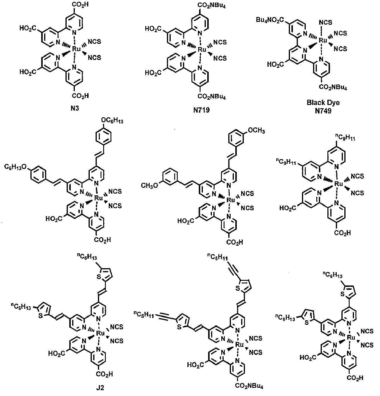

スクアリリウムシアニン色素としては、例えば、特開平11-214730号公報に記載のスクアリリウムシアニン色素(特に、段落番号0036~0047に記載の色素)、特開2012-144688号公報に記載のスクアリリウムシアニン色素(特に、段落番号0039~0046および段落番号0054~0060に記載の色素)、特開2012-84503号公報に記載のスクアリリウムシアニン色素(特に、段落番号0066~0076などに記載の色素)が挙げられる。
有機色素としては、例えば、特開2004-063274号公報に記載の有機色素(特に、段落番号0017~0021に記載の色素)、特開2005-123033号公報に記載の有機色素(特に、段落番号0021~0028に記載の色素)、特開2007-287694号公報に記載の有機色素(特に、段落番号0091~0096に記載の色素)、特開2008-71648号公報に記載の有機色素(特に、段落番号0030~0034に記載の色素)、国際公開第2007/119525号パンフレットに記載の有機色素(特に、[0024]に記載の色素)が挙げられる。
ポルフィリン色素としては、例えば、Angew. Chem. Int. Ed., 49,1~5(2010)などに記載のポルフィリン色素が挙げられる。
フタロシアニン色素としては、例えば、Angew.Chem. Int. Ed., 46,8358(2007)などに記載のフタロシアニン色素が挙げられる。
本発明においては、複数の色素を併用してもよい。併用する色素としては、上記のRu金属錯体色素、スクアリリウムシアニン色素、または有機色素が挙げられる。
色素の使用量は、全体で、支持体1m2当たり0.01~100ミリモルが好ましく、より好ましくは0.1~50ミリモル、特に好ましくは0.1~10ミリモルである。本発明で用いる色素は単独で色素増感太陽電池の増感色素として機能するものが好ましい。また、色素の半導体微粒子に対する吸着量は半導体微粒子1gに対して0.001~1ミリモルが好ましく、より好ましくは0.1~0.5ミリモルである。このような色素量とすることによって、半導体微粒子における増感効果が十分に得られる。
色素が塩である場合、対イオンは特に限定されず、上記CIの他に、例えばアルカリ金属イオン又は4級アンモニウムイオン等が挙げられる。
色素が塩である場合、対イオンは特に限定されず、上記CIの他に、例えばアルカリ金属イオン又は4級アンモニウムイオン等が挙げられる。
本発明において、半導体微粒子への色素の吸着は、後述するように、色素を含有する色素溶液を用いて行うことが好ましい。例えば、支持体上に半導体微粒子層(感光体層)を形成させた半導体電極を、色素を溶解してなる色素溶液に浸漬するなどして行うことができる。
- 本発明の化合物 -
本発明の光電変換素子および色素増感太陽電池においては、本発明の化合物を使用し、電解質に含有させるか、または、色素とともに半導体微粒子の表面に吸着させるのが好ましい。すなわち、本発明の化合物は、感光体層中、感光体層の表面、電荷移動体層中および電荷移動体層の表面の少なくともいずれか一つに含まれるのが好ましい。本発明においては、本発明の化合物を複数併用してもよい。本発明の化合物は、式(1)で表される化合物として上述した通りである。
本発明の光電変換素子および色素増感太陽電池においては、本発明の化合物を使用し、電解質に含有させるか、または、色素とともに半導体微粒子の表面に吸着させるのが好ましい。すなわち、本発明の化合物は、感光体層中、感光体層の表面、電荷移動体層中および電荷移動体層の表面の少なくともいずれか一つに含まれるのが好ましい。本発明においては、本発明の化合物を複数併用してもよい。本発明の化合物は、式(1)で表される化合物として上述した通りである。
半導体微粒子に本発明の化合物を吸着させる場合には、半導体微粒子に色素を吸着させた後に、本発明の化合物を含む後述する表面処理液を用いて半導体微粒子の表面を処理するのが好ましい。この処理により、半導体微粒子の表面に本発明の化合物を吸着させることができる。表面処理液および半導体微粒子の表面処理方法については後述する。
- 共吸着剤 -
本発明の光電変換素子においては、共吸着剤を使用し、色素とともに半導体微粒子の表面に吸着させるのが好ましい。このような共吸着剤としては酸性基(好ましくは、カルボキシ基もしくはその塩の基)を1つ以上有する共吸着剤が好ましく、脂肪酸やステロイド骨格を有する化合物が挙げられる。脂肪酸は、飽和脂肪酸でも不飽和脂肪酸でもよく、例えばブタン酸、ヘキサン酸、オクタン酸、デカン酸、ヘキサデカン酸、ドデカン酸、パルミチン酸、ステアリン酸、オレイン酸、リノール酸、リノレン酸等が挙げられる。
ステロイド骨格を有する化合物として、コール酸、グリココール酸、ケノデオキシコール酸、ヒオコール酸、デオキシコール酸、リトコール酸、ウルソデオキシコール酸等が挙げられる。好ましくはコール酸、デオキシコール酸、ケノデオキシコール酸であり、さらに好ましくはケノデオキシコール酸である。
共吸着剤としては、特開2012-012570号公報の段落番号0107に記載の化合物が好ましく、該特開2012-012570号公報の段落番号0107の記載が、そのまま本願明細書に好ましく取り込まれる。
本発明の光電変換素子においては、共吸着剤を使用し、色素とともに半導体微粒子の表面に吸着させるのが好ましい。このような共吸着剤としては酸性基(好ましくは、カルボキシ基もしくはその塩の基)を1つ以上有する共吸着剤が好ましく、脂肪酸やステロイド骨格を有する化合物が挙げられる。脂肪酸は、飽和脂肪酸でも不飽和脂肪酸でもよく、例えばブタン酸、ヘキサン酸、オクタン酸、デカン酸、ヘキサデカン酸、ドデカン酸、パルミチン酸、ステアリン酸、オレイン酸、リノール酸、リノレン酸等が挙げられる。
ステロイド骨格を有する化合物として、コール酸、グリココール酸、ケノデオキシコール酸、ヒオコール酸、デオキシコール酸、リトコール酸、ウルソデオキシコール酸等が挙げられる。好ましくはコール酸、デオキシコール酸、ケノデオキシコール酸であり、さらに好ましくはケノデオキシコール酸である。
共吸着剤としては、特開2012-012570号公報の段落番号0107に記載の化合物が好ましく、該特開2012-012570号公報の段落番号0107の記載が、そのまま本願明細書に好ましく取り込まれる。
共吸着剤は、半導体微粒子に吸着させることにより、色素の非効率な会合を抑制する効果および半導体微粒子表面から電解質中のレドックス系への逆電子移動を防止する効果がある。共吸着剤の使用量は特に限定されないが、色素1モルに対して、好ましくは1~200モル、さらに好ましくは10~150モル、特に好ましくは20~50モルであることが上記の作用を効果的に発現させられる観点から好ましい。
< 電荷移動体層 >
本発明の光電変換素子に用いられる電荷移動体層は、受光電極と対極との間に設けられる。この電荷移動体層は、色素の酸化体に電子を補充する機能を有する層である。
本発明の光電変換素子に用いられる電荷移動体層は、受光電極と対極との間に設けられる。この電荷移動体層は、色素の酸化体に電子を補充する機能を有する層である。
- 電解質 -
電荷移動体層は電解質を有する。本実施形態において電荷移動体層は電解質からなる。
電解質の例としては、酸化還元対を有機溶媒に溶解した液体電解質、酸化還元対を有機溶媒に溶解した液体をポリマーマトリクスに含浸したいわゆるゲル電解質、酸化還元対を含有する溶融塩などが挙げられる。効率を高めるためには液体電解質が好ましい。
電荷移動体層は電解質を有する。本実施形態において電荷移動体層は電解質からなる。
電解質の例としては、酸化還元対を有機溶媒に溶解した液体電解質、酸化還元対を有機溶媒に溶解した液体をポリマーマトリクスに含浸したいわゆるゲル電解質、酸化還元対を含有する溶融塩などが挙げられる。効率を高めるためには液体電解質が好ましい。
酸化還元対として、例えばヨウ素とヨウ化物(ヨウ化物塩、ヨウ化イオン性液体が好ましく、ヨウ化リチウム、ヨウ化テトラブチルアンモニウム、ヨウ化テトラプロピルアンモニウム、ヨウ化メチルプロピルイミダゾリウムが好ましい)との組み合わせ、アルキルビオローゲン(例えばメチルビオローゲンクロリド、ヘキシルビオローゲンブロミド、ベンジルビオローゲンテトラフルオロボレート)とその還元体との組み合わせ、ポリヒドロキシベンゼン類(例えばハイドロキノン、ナフトハイドロキノン等)とその酸化体との組み合わせ、2価と3価の鉄錯体の組み合せ(例えば赤血塩と黄血塩の組み合せ)、2価と3価のコバルト錯体の組み合わせ等が挙げられる。これらのうちヨウ素とヨウ化物との組み合わせ、2価と3価のコバルト錯体の組み合わせが好ましく、ヨウ素とヨウ化物との組み合わせが特に好ましい。
上記コバルト錯体は、特開2013-077449号公報の段落番号0060~0063に記載の式(A)で表される錯体が好ましく、該特開2013-077449号公報の段落番号0060~0077の記載が、そのまま本明細書に好ましく取り込まれる。
電解質として、ヨウ素とヨウ化物との組み合せを用いる場合、5員環または6員環の含窒素芳香族カチオンのヨウ素塩をさらに併用するのが好ましい。
電解質は、酸化還元対に加えて、好ましくは本発明の化合物を有する。本発明の化合物は上述した通りである。
電解質への添加物としては、本発明の化合物のほか、本発明の化合物以外のピリジン化合物、ベンズイミダゾール化合物、イミダゾール化合物、尿素誘導体、アミド化合物、ピリミジン化合物および窒素を含まない複素環を加えることができる。
酸化還元対、好適に含有される本発明の化合物、および、場合により含有される上記添加物を溶かす有機溶媒としては、特に限定されないが、非プロトン性の極性溶媒(例えばアセトニトリル、炭酸プロピレン、炭酸エチレン、ジメチルホルムアミド、ジメチルスルホキシド、スルホラン、1,3-ジメチルイミダゾリノン、3-メチルオキサゾリジノン等)が好ましい。
特に、液体電解質の有機溶媒は、ニトリル化合物、エーテル化合物、エステル化合物等が用いられ、ニトリル化合物が好ましく、アセトニトリル、メトキシプロピオニトリルが特に好ましい。
特に、液体電解質の有機溶媒は、ニトリル化合物、エーテル化合物、エステル化合物等が用いられ、ニトリル化合物が好ましく、アセトニトリル、メトキシプロピオニトリルが特に好ましい。
ゲル電解質のマトリクスに使用されるポリマー(ポリマーマトリクス)としては、例えばポリアクリロニトリル、ポリビニリデンフルオリド等が挙げられる。
溶融塩としては、例えばヨウ化リチウムと他の少なくとも1種類のリチウム塩(例えば酢酸リチウム、過塩素酸リチウム等)にポリエチレンオキシドを混合することにより、室温における流動性を付与したもの等が挙げられる。この場合のポリマーの添加量は1~50質量%である。また、γ-ブチロラクトンを電解液に含んでいてもよく、これによりヨウ化物イオンの拡散効率が高くなり光電変換効率が向上する。
溶融塩としては、例えばヨウ化リチウムと他の少なくとも1種類のリチウム塩(例えば酢酸リチウム、過塩素酸リチウム等)にポリエチレンオキシドを混合することにより、室温における流動性を付与したもの等が挙げられる。この場合のポリマーの添加量は1~50質量%である。また、γ-ブチロラクトンを電解液に含んでいてもよく、これによりヨウ化物イオンの拡散効率が高くなり光電変換効率が向上する。
また、光電変換効率を向上するために、電解液の水分を制御する方法をとってもよい。水分を制御する好ましい方法としては、濃度を制御する方法や脱水剤を共存させる方法を挙げることができる。ヨウ素の毒性軽減のために、ヨウ素とシクロデキストリンの包摂化合物の使用をしてもよく、逆に水分を常時補給する方法を用いてもよい。また環状アミジンを用いてもよく、酸化防止剤、加水分解防止剤、分解防止剤、ヨウ化亜鉛を加えてもよい。
電解質として溶融塩を用いてもよく、好ましい溶融塩としては、イミダゾリウムまたはトリアゾリウム型陽イオンを含むイオン性液体、オキサゾリウム系、ピリジニウム系、グアニジウム系およびこれらの組み合わせが挙げられる。これらカチオン系に対して特定のアニオンと組み合わせてもよい。これらの溶融塩に対しては添加物を加えてもよい。液晶性の置換基を持っていてもよい。また、四級アンモニウム塩系の溶融塩を用いてもよい。
これら以外の溶融塩としては、例えば、ヨウ化リチウムと他の少なくとも1種類のリチウム塩(例えば酢酸リチウム、過塩素酸リチウム等)にポリエチレンオキシドを混合することにより、室温における流動性を付与したもの等が挙げられる。
電解質と溶媒からなる電解液にゲル化剤を添加してゲル化させることにより、電解質を擬固体化してもよい(擬固体化された電解質を、以下、「擬固体電解質」ともいう)。ゲル化剤としては、分子量1000以下の有機化合物、分子量500~5000の範囲のSi含有化合物、特定の酸性化合物と塩基性化合物からできる有機塩、ソルビトール誘導体、ポリビニルピリジンが挙げられる。
また、マトリックス高分子、架橋型高分子化合物またはモノマー、架橋剤、電解質および溶媒を高分子中に閉じ込める方法を用いてもよい。
マトリックス高分子として好ましくは、含窒素複素環を主鎖あるいは側鎖の繰り返し単位中に持つ高分子およびこれらを求電子性化合物と反応させた架橋体、トリアジン構造を持つ高分子、ウレイド構造をもつ高分子、液晶性化合物を含むもの、エーテル結合を有する高分子、ポリフッ化ビニリデン系、メタクリレート・アクリレート系、熱硬化性樹脂、架橋ポリシロキサン、ポリビニルアルコール(PVA)、ポリアルキレングリコールとデキストリンなどの包摂化合物、含酸素または含硫黄高分子を添加した系、天然高分子などが挙げられる。これらにアルカリ膨潤型高分子、一つの高分子内にカチオン部位とヨウ素との電荷移動錯体を形成できる化合物を持った高分子などを添加してもよい。
マトリックス高分子として好ましくは、含窒素複素環を主鎖あるいは側鎖の繰り返し単位中に持つ高分子およびこれらを求電子性化合物と反応させた架橋体、トリアジン構造を持つ高分子、ウレイド構造をもつ高分子、液晶性化合物を含むもの、エーテル結合を有する高分子、ポリフッ化ビニリデン系、メタクリレート・アクリレート系、熱硬化性樹脂、架橋ポリシロキサン、ポリビニルアルコール(PVA)、ポリアルキレングリコールとデキストリンなどの包摂化合物、含酸素または含硫黄高分子を添加した系、天然高分子などが挙げられる。これらにアルカリ膨潤型高分子、一つの高分子内にカチオン部位とヨウ素との電荷移動錯体を形成できる化合物を持った高分子などを添加してもよい。
マトリックスポリマーとして2官能以上のイソシアネートと、ヒドロキシル基、アミノ基、カルボキシ基などの官能基とを反応させた架橋ポリマーを含む系を用いても良い。また、ヒドロシリル基と二重結合性化合物による架橋高分子、ポリスルホン酸またはポリカルボン酸などを2価以上の金属イオン化合物と反応させる架橋方法などを用いても良い。
上記擬固体電解質との組み合わせで好ましく用いることができる溶媒としては、特定のリン酸エステル、エチレンカーボネートを含む混合溶媒、特定の比誘電率を持つ溶媒などが挙げられる。固体電解質膜あるいは細孔に液体電解質溶液を保持させても良く、その方法として好ましくは、導電性高分子膜、繊維状固体、フィルタなどの布状固体が挙げられる。
以上の液体電解質および擬固体電解質の代わりに、p型半導体あるいはホール輸送材料などの固体電荷輸送層、例えば、CuI、CuNCSなどを用いることができる。また、Nature, vol.486,p.487,2012等に記載の電解質を用いてもよい。固体電荷輸送層として有機ホール輸送材料を用いても良い。有機ホール輸送材料として好ましくは、ポリチオフェン、ポリアニリン、ポリピロールおよびポリシランなどの導電性高分子および2個の環がC、Siなど四面体構造をとる中心元素を共有するスピロ化合物、トリアリールアミンなどの芳香族アミン誘導体、トリフェニレン誘導体、含窒素複素環誘導体、液晶性シアノ誘導体が挙げられる。
酸化還元対は、電子のキャリアになるので、ある程度の濃度を含有するのが好ましい。好ましい濃度としては合計で0.01モル/L以上であり、より好ましくは0.1モル/L以上であり、特に好ましくは0.3モル/L以上である。この場合の上限には特に制限はないが、通常5モル/L程度である。
また、本発明の化合物は、その機能を発揮するため、ある程度の濃度で含有するのが好ましい。好ましい濃度としては、0.01モル/L以上であり、より好ましくは0.1モル/L以上であり、特に好ましくは0.25モル/L以上である。この場合の上限には特に制限はないが、通常5モル/L程度である。
また、本発明の化合物は、その機能を発揮するため、ある程度の濃度で含有するのが好ましい。好ましい濃度としては、0.01モル/L以上であり、より好ましくは0.1モル/L以上であり、特に好ましくは0.25モル/L以上である。この場合の上限には特に制限はないが、通常5モル/L程度である。
< 対極 >
対極は、色素増感太陽電池(光電気化学電池)の正極として働くものであることが好ましい。対極は、通常前述の導電性支持体と同義であるが、強度が十分に保たれるような構成では支持体は必ずしも必要でない。対極の構造としては、集電効果が高い構造が好ましい。感光層に光が到達するためには、前述の導電性支持体と対極との少なくとも一方は実質的に透明でなければならない。本発明の色素増感太陽電池においては、導電性支持体が透明であって太陽光を支持体側から入射させるのが好ましい。この場合、対極は光を反射する性質を有することがさらに好ましい。色素増感太陽電池の対極としては、金属もしくは導電性の酸化物を蒸着したガラス、またはプラスチックが好ましく、白金を蒸着したガラスが特に好ましい。色素増感太陽電池では、構成物の蒸散を防止するために、電池の側面をポリマーや接着剤等で密封することが好ましい。
対極は、色素増感太陽電池(光電気化学電池)の正極として働くものであることが好ましい。対極は、通常前述の導電性支持体と同義であるが、強度が十分に保たれるような構成では支持体は必ずしも必要でない。対極の構造としては、集電効果が高い構造が好ましい。感光層に光が到達するためには、前述の導電性支持体と対極との少なくとも一方は実質的に透明でなければならない。本発明の色素増感太陽電池においては、導電性支持体が透明であって太陽光を支持体側から入射させるのが好ましい。この場合、対極は光を反射する性質を有することがさらに好ましい。色素増感太陽電池の対極としては、金属もしくは導電性の酸化物を蒸着したガラス、またはプラスチックが好ましく、白金を蒸着したガラスが特に好ましい。色素増感太陽電池では、構成物の蒸散を防止するために、電池の側面をポリマーや接着剤等で密封することが好ましい。
本発明は、特許第4260494号公報、特開2004-146425号公報、特開2000-340269号公報、特開2002-289274号公報、特開2004-152613号公報、特開平9-27352号公報に記載の光電変換素子、色素増感太陽電池に適用することができる。また、特開2004-152613号公報、特開2000-90989号公報、特開2003-217688号公報、特開2002-367686号公報、特開2003-323818号公報、特開2001-43907号公報、特開2000-340269号公報、特開2005-85500号公報、特開2004-273272号公報、特開2000-323190号公報、特開2000-228234号公報、特開2001-266963号公報、特開2001-185244号公報、特表2001-525108号公報、特開2001-203377号公報、特開2000-100483号公報、特開2001-210390号公報、特開2002-280587号公報、特開2001-273937号公報、特開2000-285977号公報、特開2001-320068号公報等に記載の光電変換素子、色素増感太陽電池に適用することができる。
<<光電変換素子用電子移動促進剤>>
本発明の光電変換素子用電子移動促進剤は、式(1)で表される化合物であり、好ましくは光電変換素子に用いられると、上述のように電圧低下を防止する効果と色素の電子移動を促進する効果を発揮する。
本発明の光電変換素子用電子移動促進剤は、光電変換素子用の電解質組成物、または、光電変換素子の半導体微粒子もしくは感光体層の表面処理液に添加されて、例えば光電変換素子を製造するのに使用される。
本発明の光電変換素子用電子移動促進剤は、式(1)で表される化合物であり、好ましくは光電変換素子に用いられると、上述のように電圧低下を防止する効果と色素の電子移動を促進する効果を発揮する。
本発明の光電変換素子用電子移動促進剤は、光電変換素子用の電解質組成物、または、光電変換素子の半導体微粒子もしくは感光体層の表面処理液に添加されて、例えば光電変換素子を製造するのに使用される。
<<電解質組成物および表面処理液>>
本発明の光電変換素子および色素増感太陽電池は、電解質組成物、および、半導体微粒子または感光体層の表面処理液の少なくとも一方を用いて、製造されるのが好ましい。電解質組成物および表面処理液は、本発明の化合物を添加剤として含有することが好ましく、より好ましくは光電変換素子用電子移動促進剤として含有する。なお、本発明の化合物は上述した通りである。
本発明の光電変換素子および色素増感太陽電池は、電解質組成物、および、半導体微粒子または感光体層の表面処理液の少なくとも一方を用いて、製造されるのが好ましい。電解質組成物および表面処理液は、本発明の化合物を添加剤として含有することが好ましく、より好ましくは光電変換素子用電子移動促進剤として含有する。なお、本発明の化合物は上述した通りである。
電解質組成物は、光電変換素子の電解質となる材料である。この電解質組成物は、電解質として、上記の液体電解質、ゲル電解質および溶融塩のいずれを含有してもよいが、液体電解質が好ましい。これらの電解質が有する成分および有機溶媒ならびに含有量は上述した通りである。
光電変換素子や色素増感太陽電池における電解質組成物の水分含有量の調整は、本発明の効果を効果的に奏するうえで好ましく、例えば、この電解質組成物の水分含有量(含有率)を0~0.1質量%に調整することがより好ましい。
この電解質組成物は、光電変換素子の製造において、感光体層と対極の間に設けられる。例えば、液体電解質であれば感光体層と対極の間に注入または流入させることができる。
光電変換素子や色素増感太陽電池における電解質組成物の水分含有量の調整は、本発明の効果を効果的に奏するうえで好ましく、例えば、この電解質組成物の水分含有量(含有率)を0~0.1質量%に調整することがより好ましい。
この電解質組成物は、光電変換素子の製造において、感光体層と対極の間に設けられる。例えば、液体電解質であれば感光体層と対極の間に注入または流入させることができる。
表面処理液は、本発明の化合物を含有していればよく、通常、溶媒を含有する組成物である。溶媒としては、特に限定されないが、上記電解質で例示したものと同じものを挙げることができる。
表面処理液が含有してもよいその他の成分として、上記添加物および共吸着剤等が挙げられる。
表面処理液中の、本発明の化合物の濃度は、特に限定されないが、例えば、0.01~1.0モル/Lが好ましく、0.05~0.5モル/Lがより好ましい。
この表面処理液は、光電変換素子の製造において、半導体微粒子または感光体層に塗布、又は浸漬液として使用される。具体的には、色素を吸着させた半導体微粒子を有する基板を、本発明の化合物を0.05モル/Lの濃度で含有するアセトニトリル溶液に30分間浸す等の方法が挙げられる。
表面処理液が含有してもよいその他の成分として、上記添加物および共吸着剤等が挙げられる。
表面処理液中の、本発明の化合物の濃度は、特に限定されないが、例えば、0.01~1.0モル/Lが好ましく、0.05~0.5モル/Lがより好ましい。
この表面処理液は、光電変換素子の製造において、半導体微粒子または感光体層に塗布、又は浸漬液として使用される。具体的には、色素を吸着させた半導体微粒子を有する基板を、本発明の化合物を0.05モル/Lの濃度で含有するアセトニトリル溶液に30分間浸す等の方法が挙げられる。
<<色素増感太陽電池の製造方法>>
本発明においては、本発明の化合物を含有する電解質組成物を用いて、電荷移動体層を設けるのが好ましい。該電解質組成物を用いて電荷移動体層を設ける方法は、特に限定されず、液体電解質の場合は上記方法が挙げられる。
また、本発明においては、本発明の化合物を含有する表面処理液を用いて、半導体微粒子または感光体層を表面処理するのが好ましい。該表面処理液を用いて半導体微粒子または感光体層を表面処理する方法は上述した通りである。
本発明においては、本発明の化合物を含有する電解質組成物を用いて、電荷移動体層を設けるのが好ましい。該電解質組成物を用いて電荷移動体層を設ける方法は、特に限定されず、液体電解質の場合は上記方法が挙げられる。
また、本発明においては、本発明の化合物を含有する表面処理液を用いて、半導体微粒子または感光体層を表面処理するのが好ましい。該表面処理液を用いて半導体微粒子または感光体層を表面処理する方法は上述した通りである。
本発明においては、色素を含有する色素溶液を使用して色素吸着電極を製造することが好ましい。このような色素溶液には、上記色素が溶媒に溶解されてなり、必要により共吸着剤や他の成分を含んでもよい。
使用する溶媒としては、特開2001-291534号公報に記載の溶媒が挙げられるが、特に限定されない。本発明においては有機溶媒が好ましく、さらにアルコール類、アミド類、ニトリル類、炭化水素類、および、これらの2種以上の混合溶媒が好ましい。混合溶媒としては、アルコール類と、アミド類、ニトリル類または炭化水素類から選択される溶媒との混合溶媒が好ましい。さらに好ましくはアルコール類とアミド類、アルコール類と炭化水素類の混合溶媒、特に好ましくはアルコール類とアミド類の混合溶媒である。
具体的にはメタノール、エタノール、プロパノール、ブタノール、ジメチルホルムアミド、ジメチルアセトアミドが好ましい。
使用する溶媒としては、特開2001-291534号公報に記載の溶媒が挙げられるが、特に限定されない。本発明においては有機溶媒が好ましく、さらにアルコール類、アミド類、ニトリル類、炭化水素類、および、これらの2種以上の混合溶媒が好ましい。混合溶媒としては、アルコール類と、アミド類、ニトリル類または炭化水素類から選択される溶媒との混合溶媒が好ましい。さらに好ましくはアルコール類とアミド類、アルコール類と炭化水素類の混合溶媒、特に好ましくはアルコール類とアミド類の混合溶媒である。
具体的にはメタノール、エタノール、プロパノール、ブタノール、ジメチルホルムアミド、ジメチルアセトアミドが好ましい。
色素溶液は共吸着剤を含有することが好ましい。
ここで、色素溶液は、光電変換素子や色素増感太陽電池を作成する際に、この溶液をこのまま使用できるように、色素や共吸着剤の濃度が調整されているものが好ましい。本発明においては、色素を0.001~0.1質量%含有することが好ましい。
ここで、色素溶液は、光電変換素子や色素増感太陽電池を作成する際に、この溶液をこのまま使用できるように、色素や共吸着剤の濃度が調整されているものが好ましい。本発明においては、色素を0.001~0.1質量%含有することが好ましい。
色素溶液は、水分含有量を調整することが特に好ましく、従って、本発明においては水の含有量(含有率)を0~0.1質量%に調整することが特に好ましい。
本発明においては、上記色素溶液を用いて、半導体電極が備える半導体微粒子表面に色素を担持させてなる色素増感太陽電池用半導体電極が好ましい。
また、上記色素溶液を用いて、半導体電極が備える半導体微粒子表面に色素を担持させることにより色素増感太陽電池を製造することが好ましい。
本発明においては、上記色素溶液を用いて、半導体電極が備える半導体微粒子表面に色素を担持させてなる色素増感太陽電池用半導体電極が好ましい。
また、上記色素溶液を用いて、半導体電極が備える半導体微粒子表面に色素を担持させることにより色素増感太陽電池を製造することが好ましい。
以下に実施例に基づき、本発明について更に詳細に説明するが、本発明がこれに限定して解釈されるものではない。
実施例1
< 色素増感太陽電池の作製 >
下記のようにして、色素増感太陽電池を作製し、光電変換効率の測定を行った。
< 色素増感太陽電池の作製 >
下記のようにして、色素増感太陽電池を作製し、光電変換効率の測定を行った。
下記化合物T1~T5、T7~T13、T21およびT22を用いた。これら化合物のうち市販されていないものは、化合物T11及び22の下記合成方法に準じて、合成した。
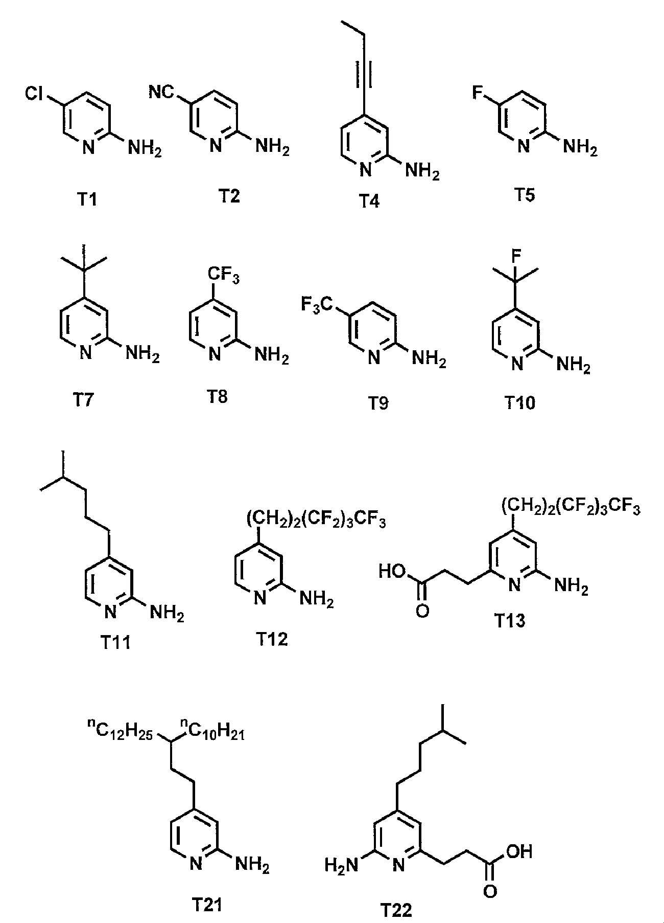
(化合物T11の合成)
下記スキームに従って化合物T11を合成した。
下記スキームに従って化合物T11を合成した。
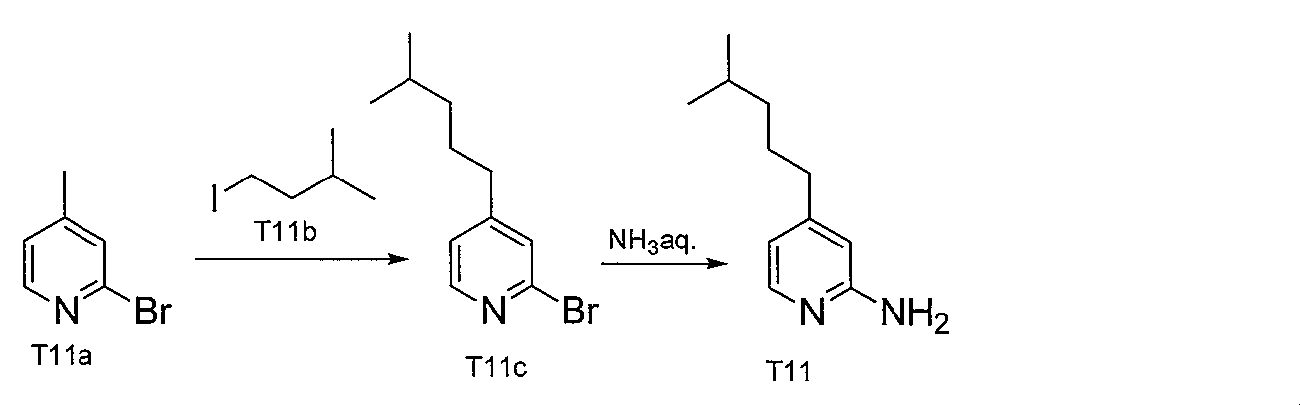
化合物11cの合成
DIPA(ジイソプロピルアミン)(9g)とTHF(50mL)を混合し、-50℃に冷却した後、1.6Mのn-BuLi(ヘキサン溶液、13.1mL)を滴下し、30分間攪拌した。続けて、T11a(3.0g)を添加し、1時間攪拌した後、化合物T11b(3.5g)を滴下し、2時間攪拌した。反応後の溶液を室温まで放冷し、さらに1時間攪拌した。攪拌後、そこへ水と酢酸エチルを加え、分液した。有機相を濃縮し、カラムクロマトグラフィーで精製して、化合物T11c(3.1g)を得た。
DIPA(ジイソプロピルアミン)(9g)とTHF(50mL)を混合し、-50℃に冷却した後、1.6Mのn-BuLi(ヘキサン溶液、13.1mL)を滴下し、30分間攪拌した。続けて、T11a(3.0g)を添加し、1時間攪拌した後、化合物T11b(3.5g)を滴下し、2時間攪拌した。反応後の溶液を室温まで放冷し、さらに1時間攪拌した。攪拌後、そこへ水と酢酸エチルを加え、分液した。有機相を濃縮し、カラムクロマトグラフィーで精製して、化合物T11c(3.1g)を得た。
化合物T11の合成
化合物T11c(2.0g)、Cu2O(60mg)、28%アンモニア水(6mL)、炭酸カリウム(220mg)およびジメチルエチレンジアミン(2mL)をエチレングリコール(20mL)中で混合し、60℃で10時間攪拌した。攪拌した混合物を冷却した後、そこへ酢酸エチルと水を加え、分液した。有機相を濃縮し、カラムクロマトグラフィーで精製して、T11(1.1g)を得た。
化合物T11の構造はMS測定およびNMRにより確認した。
MS-ESI m/z= 179.2 (M+H)+
化合物T11c(2.0g)、Cu2O(60mg)、28%アンモニア水(6mL)、炭酸カリウム(220mg)およびジメチルエチレンジアミン(2mL)をエチレングリコール(20mL)中で混合し、60℃で10時間攪拌した。攪拌した混合物を冷却した後、そこへ酢酸エチルと水を加え、分液した。有機相を濃縮し、カラムクロマトグラフィーで精製して、T11(1.1g)を得た。
化合物T11の構造はMS測定およびNMRにより確認した。
MS-ESI m/z= 179.2 (M+H)+
(化合物T22の合成)
下記のスキームに従って化合物T22を合成した。
下記のスキームに従って化合物T22を合成した。
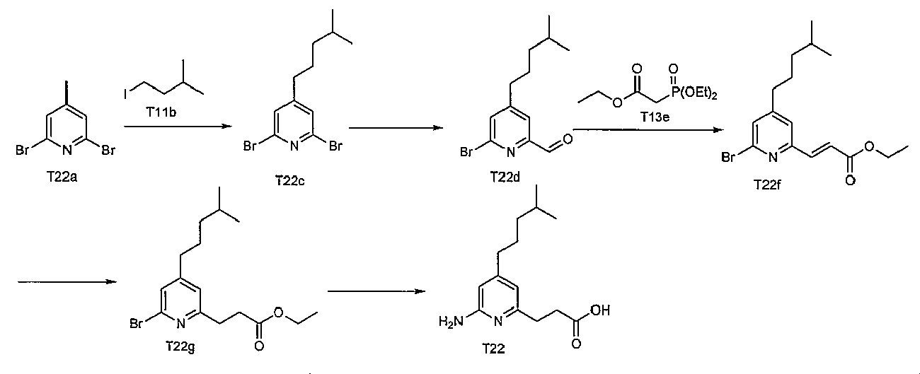
(化合物T22cの合成)
DIPA(ジイソプロピルアミン)(9g)とTHF(50mL)を混合し、-50℃に冷却した後、1.6Mのn-BuLi(ヘキサン溶液、12.0mL)を滴下して30分間攪拌した。続けて化合物T22a(4.4g)を添加し、1時間攪拌した後、化合物T11b(3.5g)を滴下し、2時間攪拌した。反応後の溶液を室温まで放冷し、さらに1時間攪拌した。攪拌後、そこへ水と酢酸エチルを加え、分液した。有機相を濃縮し、カラムクロマトグラフィーで精製して、化合物T22c(3.6g)を得た。
DIPA(ジイソプロピルアミン)(9g)とTHF(50mL)を混合し、-50℃に冷却した後、1.6Mのn-BuLi(ヘキサン溶液、12.0mL)を滴下して30分間攪拌した。続けて化合物T22a(4.4g)を添加し、1時間攪拌した後、化合物T11b(3.5g)を滴下し、2時間攪拌した。反応後の溶液を室温まで放冷し、さらに1時間攪拌した。攪拌後、そこへ水と酢酸エチルを加え、分液した。有機相を濃縮し、カラムクロマトグラフィーで精製して、化合物T22c(3.6g)を得た。
化合物T22dの合成
化合物T22c(3.5g)をTHF(50mL)に溶解して-78℃に冷却した。続けて、攪拌しながら1.6Mのn-BuLi(ヘキサン溶液、6.8mL)を滴下し2時間攪拌した。次いで、DMF(5mL)を滴下し1時間攪拌した後、水を加え室温までゆっくりと放冷した。その後、酢酸エチルを加え、分液した。有機相を濃縮し、カラムクロマトグラフィーで精製して、化合物T22d(2.0g)を得た。
化合物T22c(3.5g)をTHF(50mL)に溶解して-78℃に冷却した。続けて、攪拌しながら1.6Mのn-BuLi(ヘキサン溶液、6.8mL)を滴下し2時間攪拌した。次いで、DMF(5mL)を滴下し1時間攪拌した後、水を加え室温までゆっくりと放冷した。その後、酢酸エチルを加え、分液した。有機相を濃縮し、カラムクロマトグラフィーで精製して、化合物T22d(2.0g)を得た。
化合物T22fの合成
化合物T22d(1.9g)、炭酸カリウム(9.7g)、化合物T13e(1.9g)をTHF(200mL)中、加熱還流させながら3時間攪拌した。攪拌後の溶液を放冷した後、そこへ水と酢酸エチルを加え、分液した。有機相を濃縮し、カラムクロマトグラフィーで精製して、化合物T22f(2.1g)を得た。
化合物T22d(1.9g)、炭酸カリウム(9.7g)、化合物T13e(1.9g)をTHF(200mL)中、加熱還流させながら3時間攪拌した。攪拌後の溶液を放冷した後、そこへ水と酢酸エチルを加え、分液した。有機相を濃縮し、カラムクロマトグラフィーで精製して、化合物T22f(2.1g)を得た。
化合物T22gの合成
化合物T22f(2.0g)、CuCl(0.64g)をメタノール中で攪拌し、0℃に冷却した。続けて、NaBH4(0.46g)を添加し、2時間攪拌した。攪拌後の溶液に水と酢酸エチルを加え、分液した。有機相を濃縮し、カラムクロマトグラフィーで精製して、化合物T22g(1.5g)を得た。
化合物T22f(2.0g)、CuCl(0.64g)をメタノール中で攪拌し、0℃に冷却した。続けて、NaBH4(0.46g)を添加し、2時間攪拌した。攪拌後の溶液に水と酢酸エチルを加え、分液した。有機相を濃縮し、カラムクロマトグラフィーで精製して、化合物T22g(1.5g)を得た。
化合物T22の合成
化合物T22g(1.4g)、Cu2O(50mg)、28%アンモニア水(6mL)、炭酸カリウム(200mg)およびジメチルエチレンジアミン(1.5mL)をエチレングリコール(20mL)中で混合し、60℃で10時間攪拌した。攪拌した混合物を冷却した後、そこへ酢酸エチルと水を加え、分液した。有機相を濃縮し、カラムクロマトグラフィーで精製して、化合物T22(0.8g)を得た。
化合物T22の構造はMS測定およびNMRにより確認した。
MS-ESI m/z= 250.3 (M+H)+
化合物T22g(1.4g)、Cu2O(50mg)、28%アンモニア水(6mL)、炭酸カリウム(200mg)およびジメチルエチレンジアミン(1.5mL)をエチレングリコール(20mL)中で混合し、60℃で10時間攪拌した。攪拌した混合物を冷却した後、そこへ酢酸エチルと水を加え、分液した。有機相を濃縮し、カラムクロマトグラフィーで精製して、化合物T22(0.8g)を得た。
化合物T22の構造はMS測定およびNMRにより確認した。
MS-ESI m/z= 250.3 (M+H)+
色素として下記N749(Black Dye)を用いた。

以下に示す手順により、特開2002-289274号公報に記載の図5に示されている光電極12と同様の構成を有する光電極を作製し、さらに、同公報の図3における光電極に代えてこの光電極を用いた以外は図3の色素増感太陽電池20と同様の構成を有する10×10mmのスケールの色素増感太陽電池20を作製した。具体的な構成は図2に示した。
図2では、41が透明電極、42が半導体電極、43が透明導電膜、44が基板、45が半導体層、46が光散乱層、40が光電極、20が色素増感太陽電池、CEが対極、Eが電解質、Sがスペーサーである。
図2では、41が透明電極、42が半導体電極、43が透明導電膜、44が基板、45が半導体層、46が光散乱層、40が光電極、20が色素増感太陽電池、CEが対極、Eが電解質、Sがスペーサーである。
(ペーストの調製)
(ペーストA)球形のTiO2粒子(アナターゼ、平均粒径;25nm、以下、球形TiO2粒子Aという)を硝酸溶液に入れて撹拌することによりチタニアスラリーを調製した。次に、チタニアスラリーに増粘剤としてセルロース系バインダーを加え、混練してペーストAを調製した。
(ペースト1)球形TiO2粒子Aと、球形のTiO2粒子(アナターゼ、平均粒径;200nm、以下、球形TiO2粒子Bという)とを硝酸溶液に入れて撹拌することによりチタニアスラリーを調製した。次に、チタニアスラリーに増粘剤としてセルロース系バインダーを加え、混練してペースト1(TiO2粒子Aの質量:TiO2粒子Bの質量=30:70)を調製した。
(ペースト2)ペーストAに、棒状TiO2粒子(アナターゼ、直径;100nm、アスペクト比;5、以下、棒状TiO2粒子Cという)を混合し、棒状TiO2粒子Cの質量:ペーストAの質量=30:70のペースト2を調製した。
(ペーストA)球形のTiO2粒子(アナターゼ、平均粒径;25nm、以下、球形TiO2粒子Aという)を硝酸溶液に入れて撹拌することによりチタニアスラリーを調製した。次に、チタニアスラリーに増粘剤としてセルロース系バインダーを加え、混練してペーストAを調製した。
(ペースト1)球形TiO2粒子Aと、球形のTiO2粒子(アナターゼ、平均粒径;200nm、以下、球形TiO2粒子Bという)とを硝酸溶液に入れて撹拌することによりチタニアスラリーを調製した。次に、チタニアスラリーに増粘剤としてセルロース系バインダーを加え、混練してペースト1(TiO2粒子Aの質量:TiO2粒子Bの質量=30:70)を調製した。
(ペースト2)ペーストAに、棒状TiO2粒子(アナターゼ、直径;100nm、アスペクト比;5、以下、棒状TiO2粒子Cという)を混合し、棒状TiO2粒子Cの質量:ペーストAの質量=30:70のペースト2を調製した。
(光電極の作製)
ガラス基板44(基板44)上にフッ素ドープされたSnO2導電膜43(透明導電膜43、膜厚;500nm)を形成した透明電極41(導電性支持体)を準備した。そして、このSnO2導電膜上に、上述のペースト1をスクリーン印刷し、次いで乾燥させた。その後、空気中、450℃の条件のもとで焼成した。更に、ペースト2を用いてこのスクリーン印刷と焼成とを繰り返すことにより、SnO2導電膜上に、図2に示す半導体電極42と同様の構成の半導体電極(受光面の面積;10mm×10mm、層厚;15μm、半導体層の層厚;10μm、光散乱層の層厚;5μm、光散乱層に含有される棒状TiO2粒子Cの含有率;30質量%)(感光体層)を形成し、色素を含有していない光電極を作製した。
ガラス基板44(基板44)上にフッ素ドープされたSnO2導電膜43(透明導電膜43、膜厚;500nm)を形成した透明電極41(導電性支持体)を準備した。そして、このSnO2導電膜上に、上述のペースト1をスクリーン印刷し、次いで乾燥させた。その後、空気中、450℃の条件のもとで焼成した。更に、ペースト2を用いてこのスクリーン印刷と焼成とを繰り返すことにより、SnO2導電膜上に、図2に示す半導体電極42と同様の構成の半導体電極(受光面の面積;10mm×10mm、層厚;15μm、半導体層の層厚;10μm、光散乱層の層厚;5μm、光散乱層に含有される棒状TiO2粒子Cの含有率;30質量%)(感光体層)を形成し、色素を含有していない光電極を作製した。
(色素吸着)
次に、上記のようにして作製した光電極に上記色素(N749)を以下のようにして吸着させた。
先ず、N,N-ジメチルホルムアミド/t-BuOH=1/1を溶媒として、これに色素を、その濃度が3×10-4mol/Lとなるように溶解し、さらに共吸着剤として、ケノデオキシコール酸とコール酸の等モル混合物を色素1モルに対して20モル加え、色素溶液を調製した。この色素溶液の水分量をカール・フィッシャー滴定により測定したところ、0.01質量%未満であった。次に、この溶液に、上記で作製した半導体電極を浸漬し、これにより、半導体電極42に色素が約1.5×10-7mol/cm2吸着した光電極40を完成させた。
次に、上記のようにして作製した光電極に上記色素(N749)を以下のようにして吸着させた。
先ず、N,N-ジメチルホルムアミド/t-BuOH=1/1を溶媒として、これに色素を、その濃度が3×10-4mol/Lとなるように溶解し、さらに共吸着剤として、ケノデオキシコール酸とコール酸の等モル混合物を色素1モルに対して20モル加え、色素溶液を調製した。この色素溶液の水分量をカール・フィッシャー滴定により測定したところ、0.01質量%未満であった。次に、この溶液に、上記で作製した半導体電極を浸漬し、これにより、半導体電極42に色素が約1.5×10-7mol/cm2吸着した光電極40を完成させた。
次に、対極CEとして上記の光電極40と同様の形状と大きさを有する白金電極(Pt薄膜の厚さ;100nm)、電解質Eとして、1,2-ジメチル-3-プロピルイミダゾリウムヨージド(0.6M)、ヨウ素(0.1M)およびヨウ化リチウム(0.1M)を含む溶液と、上記本発明の化合物または比較化合物(濃度0.30モル/L)とをアセトニトリルに溶解して電解質組成物(液体電解質)を調製した。この電解質組成物の水分量をカール・フィッシャー滴定により測定したところ、0.01質量%未満であった。更に、半導体電極42の大きさに合わせた形状を有するデュポン社製のスペーサーS(商品名:「サーリン」)を準備し、特開2002-289274号公報に記載の図3に示されているように、光電極40と対極CEとスペーサーSを介して対向させ、内部に上記電解質組成物を充填して電解質Eとし、光電極40を使用した色素増感太陽電池を完成させた。
< 短絡電流JSCおよび開放電圧VOCの測定ならびに光電変換効率の評価 >
電池特性試験は、ソーラーシミュレーター(WACOM製、WXS-85H)を用い、キセノンランプからAM1.5フィルタを通した1000W/m2の擬似太陽光を照射することにより行った。I-Vテスターを用いて電流-電圧特性を測定し、光電変換効率を求めた。測定された短絡電流JSCおよび開放電圧VOC、ならびに、求められた光電変換効率を、下記の比較化合物TAに対し、以下の基準で評価した。
電池特性試験は、ソーラーシミュレーター(WACOM製、WXS-85H)を用い、キセノンランプからAM1.5フィルタを通した1000W/m2の擬似太陽光を照射することにより行った。I-Vテスターを用いて電流-電圧特性を測定し、光電変換効率を求めた。測定された短絡電流JSCおよび開放電圧VOC、ならびに、求められた光電変換効率を、下記の比較化合物TAに対し、以下の基準で評価した。
(短絡電流JSC)
AA:1.17倍以上
A:1.13倍以上1.17倍未満
B:1.10倍以上1.13倍未満
C:1.07倍以上1.10倍未満
D:1.03倍以上1.07倍未満
E:0.98倍以上1.03倍未満
AA:1.17倍以上
A:1.13倍以上1.17倍未満
B:1.10倍以上1.13倍未満
C:1.07倍以上1.10倍未満
D:1.03倍以上1.07倍未満
E:0.98倍以上1.03倍未満
(開放電圧VOC)
AA:1.15倍以上
A:1.13倍以上1.15倍未満
B:1.11倍以上1.13倍未満
C:1.08倍以上1.11倍未満
D:0.98倍以上1.08倍未満
AA:1.15倍以上
A:1.13倍以上1.15倍未満
B:1.11倍以上1.13倍未満
C:1.08倍以上1.11倍未満
D:0.98倍以上1.08倍未満
(光電変換効率)
AA:1.19倍以上
A:1.16倍以上1.19倍未満
B+:1.13倍以上1.16倍未満
B:1.11倍以上1.13倍未満
C+:1.08倍以上1.11倍未満
C:1.05倍以上1.08倍未満
D:1.03倍以上1.05倍未満
E:0.98倍以上1.03倍未満
AA:1.19倍以上
A:1.16倍以上1.19倍未満
B+:1.13倍以上1.16倍未満
B:1.11倍以上1.13倍未満
C+:1.08倍以上1.11倍未満
C:1.05倍以上1.08倍未満
D:1.03倍以上1.05倍未満
E:0.98倍以上1.03倍未満
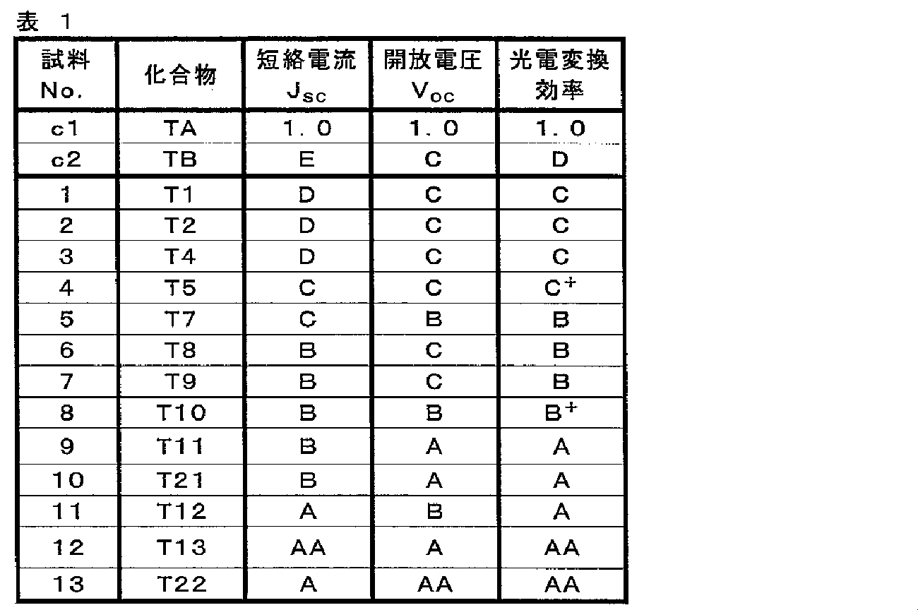

比較化合物TAは、従来用いられているt-ブチルピリジン(TBP、特許文献2に記載の比較例2)であり、比較化合物TBは、特許文献1に記載の化合物No.18である。
上記表1から明らかなように、本発明の化合物を含む本発明の色素増感太陽電池(試料No.1~13)は、短絡電流JSCが増大しており、光電変換効率に優れていることがわかった。
特に、アミノ基NR1R2と共に特定置換基Rとしてフッ素原子、および、ハロゲン原子で置換されたアルキル基を有する化合物を含む色素増感太陽電池は、短絡電流JSCがさらに増大して、より優れた光電変換効率を発揮することがわかった。
また、アミノ基NR1R2と共に特定置換基Rとして分岐アルキル基を有する化合物を含む色素増感太陽電池は、短絡電流JSCに加えて開放電圧VOCも増大して、さらに優れた光電変換効率を発揮することがわかった。
しかも、特定置換基Rが炭素数6以上の基であると、短絡電流JSCに加えて開放電圧VOCも大きく増大して、光電変換効率の大幅な向上が見られた。
また、特定置換基Rおよびアミノ基NR1R2に加えて、酸性基Acを有する化合物を含む色素増感太陽電池は、短絡電流JSCおよび開放電圧VOCが大幅に増大して、特に優れた光電変換効率を発揮することがわかった。
特に、アミノ基NR1R2と共に特定置換基Rとしてフッ素原子、および、ハロゲン原子で置換されたアルキル基を有する化合物を含む色素増感太陽電池は、短絡電流JSCがさらに増大して、より優れた光電変換効率を発揮することがわかった。
また、アミノ基NR1R2と共に特定置換基Rとして分岐アルキル基を有する化合物を含む色素増感太陽電池は、短絡電流JSCに加えて開放電圧VOCも増大して、さらに優れた光電変換効率を発揮することがわかった。
しかも、特定置換基Rが炭素数6以上の基であると、短絡電流JSCに加えて開放電圧VOCも大きく増大して、光電変換効率の大幅な向上が見られた。
また、特定置換基Rおよびアミノ基NR1R2に加えて、酸性基Acを有する化合物を含む色素増感太陽電池は、短絡電流JSCおよび開放電圧VOCが大幅に増大して、特に優れた光電変換効率を発揮することがわかった。
これに対して、t-ブチルのみを有する比較化合物TAを含む比較例の色素増感太陽電池(試料No.c1)、および、アミノ基と2つのメチル基を有する比較化合物TBを含む比較例の色素増感太陽電池(試料No.c2)は、短絡電流JSCおよび開放電圧VOCが小さく、光電変換効率も小さかった。
このように、ピリジン環に導入する置換基がt-ブチルのみである場合、および、ピリジン環に導入する置換基がアミノ基とメチル基である場合、特に短絡電流JSCが小さく、優れた光電変換効率が得られないことが確認された。比較化合物TA、および比較化合物TBは、半導体微粒子に対する吸着力が十分ではなく、また再配列エネルギーを低下させることができず、電子移動効率を改善できないことに起因すると考えられる。
このように、ピリジン環に導入する置換基がt-ブチルのみである場合、および、ピリジン環に導入する置換基がアミノ基とメチル基である場合、特に短絡電流JSCが小さく、優れた光電変換効率が得られないことが確認された。比較化合物TA、および比較化合物TBは、半導体微粒子に対する吸着力が十分ではなく、また再配列エネルギーを低下させることができず、電子移動効率を改善できないことに起因すると考えられる。
1 導電性支持体
2 感光体層
21 色素
22 半導体微粒子
3 電荷移動体層
4 対極
5 受光電極
6 回路
10 光電変換素子
100 色素増感太陽電池を利用したシステム
M 電動モーター
2 感光体層
21 色素
22 半導体微粒子
3 電荷移動体層
4 対極
5 受光電極
6 回路
10 光電変換素子
100 色素増感太陽電池を利用したシステム
M 電動モーター
20 色素増感太陽電池
40 光電極
41 透明電極
42 半導体電極
43 透明導電膜
44 基板
45 半導体層
46 光散乱層
CE 対極
E 電解質
S スペーサー
40 光電極
41 透明電極
42 半導体電極
43 透明導電膜
44 基板
45 半導体層
46 光散乱層
CE 対極
E 電解質
S スペーサー
Claims (12)
- 導電性支持体上に、色素が担持された半導体微粒子を有する感光体層と、電解質を含む電荷移動体層と、対極とをこの順で有する光電変換素子であって、前記導電性支持体および前記対極の間に下記式(1)で表される化合物を含む光電変換素子。

- 前記Rが、分岐アルキル基、ハロゲン原子で置換されたアルキル基、分岐アルケニル基、ハロゲン原子で置換されたアルケニル基、直鎖もしくは分岐アルキニル基またはハロゲン原子で置換されたアルキニル基である請求項1に記載の光電変換素子。
- 前記Rが、分岐アルキル基である請求項1または2に記載の光電変換素子。
- 前記Rが、ハロゲン原子で置換されたアルキル基、分岐アルケニル基、ハロゲン原子で置換されたアルケニル基、直鎖もしくは分岐アルキニル基またはハロゲン原子で置換されたアルキニル基である請求項1または2に記載の光電変換素子。
- 前記分岐アルキル基、ハロゲン原子で置換されたアルキル基、分岐アルケニル基、ハロゲン原子で置換されたアルケニル基、直鎖もしくは分岐アルキニル基またはハロゲン原子で置換されたアルキニル基の炭素数が6~30である請求項1~4のいずれか1項に記載の光電変換素子。
- 前記ハロゲン原子で置換された、アルキル基、アルケニル基もしくはアルキニル基の該ハロゲン原子、または、前記Rの前記ハロゲン原子が、フッ素原子である請求項1~5のいずれか1項に記載の光電変換素子。
- 前記式(1)で表される化合物が、少なくとも1つの酸性基を有する請求項1~6のいずれか1項に記載の光電変換素子。
- 前記n1が1以上3以下の整数であるか、または、前記R1およびR2の少なくとも一方が酸性基を有する置換基である請求項7に記載の光電変換素子。
- 前記酸性基が、カルボキシ基である請求項1~8のいずれか1項に記載の光電変換素子。
- 前記式(1)で表される化合物が、前記電解質中、および、前記半導体微粒子の表面の少なくとも一方に含まれる請求項1~9のいずれか1項に記載の光電変換素子。
- 請求項1~10のいずれか1項に記載の光電変換素子を具備する色素増感太陽電池。
- 下記式(1)で表される光電変換素子用電子移動促進剤。

Applications Claiming Priority (2)
| Application Number | Priority Date | Filing Date | Title |
|---|---|---|---|
| JP2013184494A JP6063361B2 (ja) | 2013-09-05 | 2013-09-05 | 光電変換素子、色素増感太陽電池および光電変換素子用電子移動促進剤 |
| JP2013-184494 | 2013-09-05 |
Publications (1)
| Publication Number | Publication Date |
|---|---|
| WO2015033749A1 true WO2015033749A1 (ja) | 2015-03-12 |
Family
ID=52628229
Family Applications (1)
| Application Number | Title | Priority Date | Filing Date |
|---|---|---|---|
| PCT/JP2014/071356 Ceased WO2015033749A1 (ja) | 2013-09-05 | 2014-08-13 | 光電変換素子、色素増感太陽電池および光電変換素子用電子移動促進剤 |
Country Status (3)
| Country | Link |
|---|---|
| JP (1) | JP6063361B2 (ja) |
| TW (1) | TW201509914A (ja) |
| WO (1) | WO2015033749A1 (ja) |
Citations (7)
| Publication number | Priority date | Publication date | Assignee | Title |
|---|---|---|---|---|
| JP2004047229A (ja) * | 2002-07-10 | 2004-02-12 | National Institute Of Advanced Industrial & Technology | アミノピリジン系化合物を含む電解質溶液を用いた光電変換素子及びそれを用いた色素増感型太陽電池 |
| JP2005516365A (ja) * | 2002-01-25 | 2005-06-02 | コナルカ テクノロジーズ インコーポレイテッド | 太陽電池要素及び材料 |
| WO2009113677A1 (ja) * | 2008-03-14 | 2009-09-17 | ステラケミファ株式会社 | 低腐食性イオン液体及びそれを含む潤滑油組成物 |
| JP2010015994A (ja) * | 1999-08-04 | 2010-01-21 | Fujifilm Corp | イミダゾリウム化合物及びピリジニウム化合物 |
| JP2011108628A (ja) * | 2009-11-13 | 2011-06-02 | Ind Technol Res Inst | ゲル電解質組成およびその製造方法、ならびにそれを用いた色素増感太陽電池 |
| JP2012243436A (ja) * | 2011-05-17 | 2012-12-10 | Sony Corp | 光電変換素子およびその製造方法ならびに電子機器 |
| WO2013035630A1 (ja) * | 2011-09-08 | 2013-03-14 | 富士フイルム株式会社 | 色素、これを用いた光電変換素子及び光電気化学電池 |
-
2013
- 2013-09-05 JP JP2013184494A patent/JP6063361B2/ja not_active Expired - Fee Related
-
2014
- 2014-08-13 WO PCT/JP2014/071356 patent/WO2015033749A1/ja not_active Ceased
- 2014-09-03 TW TW103130326A patent/TW201509914A/zh unknown
Patent Citations (7)
| Publication number | Priority date | Publication date | Assignee | Title |
|---|---|---|---|---|
| JP2010015994A (ja) * | 1999-08-04 | 2010-01-21 | Fujifilm Corp | イミダゾリウム化合物及びピリジニウム化合物 |
| JP2005516365A (ja) * | 2002-01-25 | 2005-06-02 | コナルカ テクノロジーズ インコーポレイテッド | 太陽電池要素及び材料 |
| JP2004047229A (ja) * | 2002-07-10 | 2004-02-12 | National Institute Of Advanced Industrial & Technology | アミノピリジン系化合物を含む電解質溶液を用いた光電変換素子及びそれを用いた色素増感型太陽電池 |
| WO2009113677A1 (ja) * | 2008-03-14 | 2009-09-17 | ステラケミファ株式会社 | 低腐食性イオン液体及びそれを含む潤滑油組成物 |
| JP2011108628A (ja) * | 2009-11-13 | 2011-06-02 | Ind Technol Res Inst | ゲル電解質組成およびその製造方法、ならびにそれを用いた色素増感太陽電池 |
| JP2012243436A (ja) * | 2011-05-17 | 2012-12-10 | Sony Corp | 光電変換素子およびその製造方法ならびに電子機器 |
| WO2013035630A1 (ja) * | 2011-09-08 | 2013-03-14 | 富士フイルム株式会社 | 色素、これを用いた光電変換素子及び光電気化学電池 |
Also Published As
| Publication number | Publication date |
|---|---|
| JP6063361B2 (ja) | 2017-01-18 |
| TW201509914A (zh) | 2015-03-16 |
| JP2015053148A (ja) | 2015-03-19 |
Similar Documents
| Publication | Publication Date | Title |
|---|---|---|
| JP6047513B2 (ja) | 金属錯体色素、光電変換素子、色素増感太陽電池および金属錯体色素を含有する色素溶液 | |
| JP5925541B2 (ja) | 光電変換素子用金属錯体色素、光電変換素子、色素増感太陽電池、色素増感太陽電池用色素吸着組成液、色素増感太陽電池用半導体電極および色素増感太陽電池の製造方法 | |
| WO2014168165A1 (ja) | 光電変換素子、色素増感太陽電池、金属錯体色素、色素溶液、色素吸着電極および色素増感太陽電池の製造方法 | |
| WO2014077357A1 (ja) | 金属錯体、金属錯体色素、光電変換素子、色素増感太陽電池、色素溶液、色素吸着電極および色素増感太陽電池の製造方法 | |
| JP2014209606A (ja) | 光電変換素子、色素増感太陽電池、金属錯体色素を含有する色素吸着液および光電変換素子の製造方法 | |
| JP6005678B2 (ja) | 金属錯体色素、光電変換素子、色素増感太陽電池および金属錯体色素を含有する色素溶液 | |
| CN104885171B (zh) | 光电转换元件、金属络合物色素、色素溶液、色素吸附电极及色素增感太阳电池及其制法 | |
| JP5913222B2 (ja) | 光電変換素子および色素増感太陽電池 | |
| WO2014050527A1 (ja) | 光電変換素子および色素増感太陽電池 | |
| JP6026236B2 (ja) | 金属錯体色素、光電変換素子、色素増感太陽電池、色素溶液、色素吸着電極及び色素増感太陽電池の製造方法 | |
| JP6009484B2 (ja) | 光電変換素子、色素増感太陽電池およびこれに用いる金属錯体色素 | |
| JP5913223B2 (ja) | 金属錯体色素、光電変換素子、色素増感太陽電池、色素溶液および色素吸着電極 | |
| JP6253167B2 (ja) | 光電変換素子、色素増感太陽電池、ルテニウム錯体色素および色素溶液 | |
| WO2014168163A1 (ja) | 光電変換素子、色素増感太陽電池、金属錯体色素、色素溶液、色素吸着電極および色素増感太陽電池の製造方法 | |
| JP2014186976A (ja) | 光電変換素子、色素増感太陽電池、金属錯体、金属錯体色素、色素溶液、色素吸着電極および色素増感太陽電池の製造方法 | |
| WO2015002081A1 (ja) | 光電変換素子、色素増感太陽電池、金属錯体色素、配位子、色素溶液、色素吸着電極および色素増感太陽電池の製造方法 | |
| JP6063361B2 (ja) | 光電変換素子、色素増感太陽電池および光電変換素子用電子移動促進剤 | |
| JP6144619B2 (ja) | 光電変換素子、色素増感太陽電池およびこれに用いる金属錯体色素 | |
| WO2015033698A1 (ja) | 光電変換素子、色素増感太陽電池および光電変換素子用逆電子移動防止剤 | |
| WO2016052196A1 (ja) | 光電変換素子、色素増感太陽電池、金属錯体色素、色素溶液、およびターピリジン化合物またはそのエステル化物 | |
| WO2016047344A1 (ja) | 光電変換素子、色素増感太陽電池、金属錯体色素および色素溶液 | |
| JP2015053150A (ja) | 光電変換素子および色素増感太陽電池 | |
| JP2016076585A (ja) | 光電変換素子、色素増感太陽電池、ルテニウム錯体色素および色素溶液 |
Legal Events
| Date | Code | Title | Description |
|---|---|---|---|
| 121 | Ep: the epo has been informed by wipo that ep was designated in this application |
Ref document number: 14842735 Country of ref document: EP Kind code of ref document: A1 |
|
| NENP | Non-entry into the national phase |
Ref country code: DE |
|
| 122 | Ep: pct application non-entry in european phase |
Ref document number: 14842735 Country of ref document: EP Kind code of ref document: A1 |