WO2015030176A1 - 応力表示部材および応力表示部材を用いたひずみ測定方法 - Google Patents
応力表示部材および応力表示部材を用いたひずみ測定方法 Download PDFInfo
- Publication number
- WO2015030176A1 WO2015030176A1 PCT/JP2014/072743 JP2014072743W WO2015030176A1 WO 2015030176 A1 WO2015030176 A1 WO 2015030176A1 JP 2014072743 W JP2014072743 W JP 2014072743W WO 2015030176 A1 WO2015030176 A1 WO 2015030176A1
- Authority
- WO
- WIPO (PCT)
- Prior art keywords
- layer
- liquid crystal
- display member
- stress display
- circularly polarized
- Prior art date
- Legal status (The legal status is an assumption and is not a legal conclusion. Google has not performed a legal analysis and makes no representation as to the accuracy of the status listed.)
- Ceased
Links
Images

Classifications
-
- G—PHYSICS
- G01—MEASURING; TESTING
- G01B—MEASURING LENGTH, THICKNESS OR SIMILAR LINEAR DIMENSIONS; MEASURING ANGLES; MEASURING AREAS; MEASURING IRREGULARITIES OF SURFACES OR CONTOURS
- G01B11/00—Measuring arrangements characterised by the use of optical techniques
- G01B11/16—Measuring arrangements characterised by the use of optical techniques for measuring the deformation in a solid, e.g. optical strain gauge
-
- G—PHYSICS
- G01—MEASURING; TESTING
- G01L—MEASURING FORCE, STRESS, TORQUE, WORK, MECHANICAL POWER, MECHANICAL EFFICIENCY, OR FLUID PRESSURE
- G01L1/00—Measuring force or stress, in general
- G01L1/24—Measuring force or stress, in general by measuring variations of optical properties of material when it is stressed, e.g. by photoelastic stress analysis using infrared, visible light, ultraviolet
- G01L1/241—Measuring force or stress, in general by measuring variations of optical properties of material when it is stressed, e.g. by photoelastic stress analysis using infrared, visible light, ultraviolet by photoelastic stress analysis
-
- G—PHYSICS
- G02—OPTICS
- G02B—OPTICAL ELEMENTS, SYSTEMS OR APPARATUS
- G02B5/00—Optical elements other than lenses
- G02B5/30—Polarising elements
-
- G—PHYSICS
- G02—OPTICS
- G02B—OPTICAL ELEMENTS, SYSTEMS OR APPARATUS
- G02B5/00—Optical elements other than lenses
- G02B5/30—Polarising elements
- G02B5/3016—Polarising elements involving passive liquid crystal elements
-
- G—PHYSICS
- G02—OPTICS
- G02F—OPTICAL DEVICES OR ARRANGEMENTS FOR THE CONTROL OF LIGHT BY MODIFICATION OF THE OPTICAL PROPERTIES OF THE MEDIA OF THE ELEMENTS INVOLVED THEREIN; NON-LINEAR OPTICS; FREQUENCY-CHANGING OF LIGHT; OPTICAL LOGIC ELEMENTS; OPTICAL ANALOGUE/DIGITAL CONVERTERS
- G02F1/00—Devices or arrangements for the control of the intensity, colour, phase, polarisation or direction of light arriving from an independent light source, e.g. switching, gating or modulating; Non-linear optics
- G02F1/01—Devices or arrangements for the control of the intensity, colour, phase, polarisation or direction of light arriving from an independent light source, e.g. switching, gating or modulating; Non-linear optics for the control of the intensity, phase, polarisation or colour
- G02F1/0128—Devices or arrangements for the control of the intensity, colour, phase, polarisation or direction of light arriving from an independent light source, e.g. switching, gating or modulating; Non-linear optics for the control of the intensity, phase, polarisation or colour based on electro-mechanical, magneto-mechanical, elasto-optic effects
- G02F1/0131—Devices or arrangements for the control of the intensity, colour, phase, polarisation or direction of light arriving from an independent light source, e.g. switching, gating or modulating; Non-linear optics for the control of the intensity, phase, polarisation or colour based on electro-mechanical, magneto-mechanical, elasto-optic effects based on photo-elastic effects, e.g. mechanically induced birefringence
-
- G—PHYSICS
- G02—OPTICS
- G02F—OPTICAL DEVICES OR ARRANGEMENTS FOR THE CONTROL OF LIGHT BY MODIFICATION OF THE OPTICAL PROPERTIES OF THE MEDIA OF THE ELEMENTS INVOLVED THEREIN; NON-LINEAR OPTICS; FREQUENCY-CHANGING OF LIGHT; OPTICAL LOGIC ELEMENTS; OPTICAL ANALOGUE/DIGITAL CONVERTERS
- G02F1/00—Devices or arrangements for the control of the intensity, colour, phase, polarisation or direction of light arriving from an independent light source, e.g. switching, gating or modulating; Non-linear optics
- G02F1/01—Devices or arrangements for the control of the intensity, colour, phase, polarisation or direction of light arriving from an independent light source, e.g. switching, gating or modulating; Non-linear optics for the control of the intensity, phase, polarisation or colour
- G02F1/13—Devices or arrangements for the control of the intensity, colour, phase, polarisation or direction of light arriving from an independent light source, e.g. switching, gating or modulating; Non-linear optics for the control of the intensity, phase, polarisation or colour based on liquid crystals, e.g. single liquid crystal display cells
-
- G—PHYSICS
- G02—OPTICS
- G02F—OPTICAL DEVICES OR ARRANGEMENTS FOR THE CONTROL OF LIGHT BY MODIFICATION OF THE OPTICAL PROPERTIES OF THE MEDIA OF THE ELEMENTS INVOLVED THEREIN; NON-LINEAR OPTICS; FREQUENCY-CHANGING OF LIGHT; OPTICAL LOGIC ELEMENTS; OPTICAL ANALOGUE/DIGITAL CONVERTERS
- G02F1/00—Devices or arrangements for the control of the intensity, colour, phase, polarisation or direction of light arriving from an independent light source, e.g. switching, gating or modulating; Non-linear optics
- G02F1/01—Devices or arrangements for the control of the intensity, colour, phase, polarisation or direction of light arriving from an independent light source, e.g. switching, gating or modulating; Non-linear optics for the control of the intensity, phase, polarisation or colour
- G02F1/13—Devices or arrangements for the control of the intensity, colour, phase, polarisation or direction of light arriving from an independent light source, e.g. switching, gating or modulating; Non-linear optics for the control of the intensity, phase, polarisation or colour based on liquid crystals, e.g. single liquid crystal display cells
- G02F1/133—Constructional arrangements; Operation of liquid crystal cells; Circuit arrangements
- G02F1/1333—Constructional arrangements; Manufacturing methods
- G02F1/1335—Structural association of cells with optical devices, e.g. polarisers or reflectors
- G02F1/13363—Birefringent elements, e.g. for optical compensation
-
- G—PHYSICS
- G02—OPTICS
- G02F—OPTICAL DEVICES OR ARRANGEMENTS FOR THE CONTROL OF LIGHT BY MODIFICATION OF THE OPTICAL PROPERTIES OF THE MEDIA OF THE ELEMENTS INVOLVED THEREIN; NON-LINEAR OPTICS; FREQUENCY-CHANGING OF LIGHT; OPTICAL LOGIC ELEMENTS; OPTICAL ANALOGUE/DIGITAL CONVERTERS
- G02F1/00—Devices or arrangements for the control of the intensity, colour, phase, polarisation or direction of light arriving from an independent light source, e.g. switching, gating or modulating; Non-linear optics
- G02F1/01—Devices or arrangements for the control of the intensity, colour, phase, polarisation or direction of light arriving from an independent light source, e.g. switching, gating or modulating; Non-linear optics for the control of the intensity, phase, polarisation or colour
- G02F1/13—Devices or arrangements for the control of the intensity, colour, phase, polarisation or direction of light arriving from an independent light source, e.g. switching, gating or modulating; Non-linear optics for the control of the intensity, phase, polarisation or colour based on liquid crystals, e.g. single liquid crystal display cells
- G02F1/137—Devices or arrangements for the control of the intensity, colour, phase, polarisation or direction of light arriving from an independent light source, e.g. switching, gating or modulating; Non-linear optics for the control of the intensity, phase, polarisation or colour based on liquid crystals, e.g. single liquid crystal display cells characterised by the electro-optical or magneto-optical effect, e.g. field-induced phase transition, orientation effect, guest-host interaction or dynamic scattering
- G02F1/13718—Devices or arrangements for the control of the intensity, colour, phase, polarisation or direction of light arriving from an independent light source, e.g. switching, gating or modulating; Non-linear optics for the control of the intensity, phase, polarisation or colour based on liquid crystals, e.g. single liquid crystal display cells characterised by the electro-optical or magneto-optical effect, e.g. field-induced phase transition, orientation effect, guest-host interaction or dynamic scattering based on a change of the texture state of a cholesteric liquid crystal
-
- B—PERFORMING OPERATIONS; TRANSPORTING
- B32—LAYERED PRODUCTS
- B32B—LAYERED PRODUCTS, i.e. PRODUCTS BUILT-UP OF STRATA OF FLAT OR NON-FLAT, e.g. CELLULAR OR HONEYCOMB, FORM
- B32B2307/00—Properties of the layers or laminate
- B32B2307/40—Properties of the layers or laminate having particular optical properties
- B32B2307/416—Reflective
-
- C—CHEMISTRY; METALLURGY
- C09—DYES; PAINTS; POLISHES; NATURAL RESINS; ADHESIVES; COMPOSITIONS NOT OTHERWISE PROVIDED FOR; APPLICATIONS OF MATERIALS NOT OTHERWISE PROVIDED FOR
- C09K—MATERIALS FOR MISCELLANEOUS APPLICATIONS, NOT PROVIDED FOR ELSEWHERE
- C09K19/00—Liquid crystal materials
- C09K19/02—Liquid crystal materials characterised by optical, electrical or physical properties of the components, in general
- C09K19/0208—Twisted Nematic (T.N.); Super Twisted Nematic (S.T.N.); Optical Mode Interference (O.M.I.)
-
- C—CHEMISTRY; METALLURGY
- C09—DYES; PAINTS; POLISHES; NATURAL RESINS; ADHESIVES; COMPOSITIONS NOT OTHERWISE PROVIDED FOR; APPLICATIONS OF MATERIALS NOT OTHERWISE PROVIDED FOR
- C09K—MATERIALS FOR MISCELLANEOUS APPLICATIONS, NOT PROVIDED FOR ELSEWHERE
- C09K19/00—Liquid crystal materials
- C09K19/04—Liquid crystal materials characterised by the chemical structure of the liquid crystal components, e.g. by a specific unit
- C09K19/36—Steroidal liquid crystal compounds
-
- G—PHYSICS
- G01—MEASURING; TESTING
- G01B—MEASURING LENGTH, THICKNESS OR SIMILAR LINEAR DIMENSIONS; MEASURING ANGLES; MEASURING AREAS; MEASURING IRREGULARITIES OF SURFACES OR CONTOURS
- G01B11/00—Measuring arrangements characterised by the use of optical techniques
- G01B11/16—Measuring arrangements characterised by the use of optical techniques for measuring the deformation in a solid, e.g. optical strain gauge
- G01B11/165—Measuring arrangements characterised by the use of optical techniques for measuring the deformation in a solid, e.g. optical strain gauge by means of a grating deformed by the object
-
- G—PHYSICS
- G01—MEASURING; TESTING
- G01B—MEASURING LENGTH, THICKNESS OR SIMILAR LINEAR DIMENSIONS; MEASURING ANGLES; MEASURING AREAS; MEASURING IRREGULARITIES OF SURFACES OR CONTOURS
- G01B11/00—Measuring arrangements characterised by the use of optical techniques
- G01B11/16—Measuring arrangements characterised by the use of optical techniques for measuring the deformation in a solid, e.g. optical strain gauge
- G01B11/168—Measuring arrangements characterised by the use of optical techniques for measuring the deformation in a solid, e.g. optical strain gauge by means of polarisation
-
- G—PHYSICS
- G01—MEASURING; TESTING
- G01B—MEASURING LENGTH, THICKNESS OR SIMILAR LINEAR DIMENSIONS; MEASURING ANGLES; MEASURING AREAS; MEASURING IRREGULARITIES OF SURFACES OR CONTOURS
- G01B11/00—Measuring arrangements characterised by the use of optical techniques
- G01B11/16—Measuring arrangements characterised by the use of optical techniques for measuring the deformation in a solid, e.g. optical strain gauge
- G01B11/18—Measuring arrangements characterised by the use of optical techniques for measuring the deformation in a solid, e.g. optical strain gauge using photoelastic elements
-
- G—PHYSICS
- G02—OPTICS
- G02F—OPTICAL DEVICES OR ARRANGEMENTS FOR THE CONTROL OF LIGHT BY MODIFICATION OF THE OPTICAL PROPERTIES OF THE MEDIA OF THE ELEMENTS INVOLVED THEREIN; NON-LINEAR OPTICS; FREQUENCY-CHANGING OF LIGHT; OPTICAL LOGIC ELEMENTS; OPTICAL ANALOGUE/DIGITAL CONVERTERS
- G02F1/00—Devices or arrangements for the control of the intensity, colour, phase, polarisation or direction of light arriving from an independent light source, e.g. switching, gating or modulating; Non-linear optics
- G02F1/01—Devices or arrangements for the control of the intensity, colour, phase, polarisation or direction of light arriving from an independent light source, e.g. switching, gating or modulating; Non-linear optics for the control of the intensity, phase, polarisation or colour
- G02F1/13—Devices or arrangements for the control of the intensity, colour, phase, polarisation or direction of light arriving from an independent light source, e.g. switching, gating or modulating; Non-linear optics for the control of the intensity, phase, polarisation or colour based on liquid crystals, e.g. single liquid crystal display cells
- G02F1/133—Constructional arrangements; Operation of liquid crystal cells; Circuit arrangements
- G02F1/1333—Constructional arrangements; Manufacturing methods
- G02F1/1335—Structural association of cells with optical devices, e.g. polarisers or reflectors
- G02F1/133528—Polarisers
- G02F1/133543—Cholesteric polarisers
Definitions
- the present invention relates to a stress display member and a strain measurement method using the stress display member. More specifically, the present invention relates to a stress display member including a cholesteric liquid crystal layer formed from a composition including a polymerizable cholesteric liquid crystal compound, and a strain measurement method using the stress display member.
- Patent Document 1 discloses a stress (strain) measurement method using selective wavelength reflectivity of cholesteric liquid crystal. In this method, stress can be measured from the color change of reflected light.
- Patent Document 2 discloses a strain measurement method using a strain sensor film composed of particles (monodispersed polystyrene) periodically and uniformly arranged by self-assembly and an elastic body (polydimethylsilicone) filling the space between the particles. Is disclosed. In this method, since the strain distribution is visualized, a special display device such as an optical microscope, a scanning electron microscope, or a laser device is unnecessary and simple.
- a method using a strain gauge is widely used because of its high quantitativeness.
- point measurement when measuring a large area in order to evaluate strain distribution, the number of measurement points increases, and it is necessary to prepare for a large number of measuring devices because of the trouble of wiring and the like.
- electric signals are processed and measured, there is a problem that distortion cannot be visualized and judged on site.
- a strain distribution generated in a plastic model can be visualized with polarized light.
- high-precision measurement cannot be performed, and there is a problem that a polarization measuring device is expensive.
- the photoelastic resin can be attached to the object to be measured, and the strain can be measured directly.
- the polarization measuring device is expensive and the strain distribution can be visualized visually. I can't.
- the stress coating method can measure strain of complex shapes by applying a brittle paint, and can evaluate the strain distribution.
- the quantitative method is low. Since the drying conditions of the paint also affect the measurement accuracy, high-precision measurement is difficult.
- An object of the present invention is to provide a novel stress display member and a novel strain measurement method using the stress display member. More specifically, an object of the present invention is to provide a stress display member that can measure strain generated in a large-area object at low cost and enables strain measurement with high measurement accuracy.
- the present inventors have intensively studied, and by using a member including a cholesteric liquid crystal layer formed using a polymerizable liquid crystal compound, distortion generated in a large-area object is highly accurate. Based on this finding, the present invention was completed. That is, the present invention provides the following [1] to [22].
- a selective reflection layer is included, and the selective reflection layer includes one or more cholesteric liquid crystal layers obtained by curing a liquid crystal composition containing a polymerizable liquid crystal compound, and the selective reflection layer is a right circularly polarized light having a selective reflection wavelength.
- a stress display member that is a layer that selectively reflects the circularly polarized light of either sense of left circularly polarized light.
- the polymerizable liquid crystal compound includes a polyfunctional liquid crystal compound having two or more polymerizable groups and a monofunctional liquid crystal compound having only one polymerizable group, the polyfunctional liquid crystal compound and the above The stress display member according to [1], wherein the mass ratio with respect to the monofunctional liquid crystal compound is 30/70 to 99/1.
- the birefringent layer has an absolute value of a photoelastic coefficient represented by a unit Pa ⁇ 1 of 20 ⁇ 10 ⁇ 12 or more and 1 ⁇ 10 ⁇ 6 or less.
- the circularly polarized light sense transmitted by the circularly polarized light separating layer is opposite to the circularly polarized light sense selectively reflected by the selective reflection layer.
- the stress display member includes a cholesteric liquid crystal layer obtained by curing a liquid crystal composition including a polymerizable liquid crystal compound.
- the selective reflection layer includes two or more cholesteric liquid crystal layers obtained by curing a liquid crystal composition containing a polymerizable liquid crystal compound, and the spiral pitch of the two or more cholesteric liquid crystal layers is different.
- the stress display member, the light shielding film, and the object according to any one of [1] to [16] are arranged in this order, and the stress display member, the light shielding film, the object, And measuring the reflected light obtained by irradiating the stress display member with light.
- [20] Adhering the stress display member according to any one of [3] to [14] to an object and irradiating the stress display member with circularly polarized light in a wavelength range including the selective reflection wavelength.
- a method for measuring strain of the object comprising measuring the obtained reflected light.
- [21] Adhering the stress display member according to any one of [1] to [17] to an object, and measuring reflected light or transmitted light obtained by irradiating the stress display member with light.
- the peak wavelength of the irradiated light is within a wavelength range where the selective reflection layer selectively reflects light, and the wavelength range of the irradiated light selectively reflects the selective reflection layer.
- the distortion measuring method of the said target object smaller than the wavelength range to perform.
- a novel stress display member and a novel strain measurement method using the stress display member are provided.
- the stress display member of the present invention it is possible to measure the strain generated in a large-area object at low cost and with high accuracy.
- ⁇ is used to mean that the numerical values described before and after it are included as a lower limit value and an upper limit value.
- “selective” for circularly polarized light means that the amount of light of either the right circularly polarized component or the left circularly polarized component of the irradiated light is greater than that of the other circularly polarized component.
- the degree of circular polarization of light is preferably 0.3 or more, more preferably 0.6 or more, and even more preferably 0.8 or more. More preferably, it is substantially 1.0.
- sense for circularly polarized light means right circularly polarized light or left circularly polarized light.
- the sense of circularly polarized light is right-handed circularly polarized light when the electric field vector tip turns clockwise as time increases when viewed as the light travels toward you, and left when it turns counterclockwise. Defined as being circularly polarized.
- the term “sense” is sometimes used for the twist direction of the spiral of the cholesteric liquid crystal.
- the selective reflection by the cholesteric liquid crystal reflects right circularly polarized light when the twist direction (sense) of the cholesteric liquid crystal spiral is right, transmits left circularly polarized light, and reflects left circularly polarized light when the sense is left, Transmits circularly polarized light.
- the polarization state of each wavelength of light can be measured using a spectral radiance meter or a spectrometer equipped with a circularly polarizing plate.
- the intensity of light measured through the right circularly polarizing plate corresponds to I R
- the intensity of light measured through the left circularly polarizing plate corresponds to I L.
- ordinary light sources such as incandescent bulbs, mercury lamps, fluorescent lamps, and LEDs emit almost natural light, but the characteristics that are attached to these to produce the polarization of the polarization state control member are, for example, a polarization phase difference manufactured by AXOMETRICS. It can be measured using an analyzer AxoScan or the like.
- a circularly polarizing plate is attached to an illuminance meter or an optical spectrum meter, it can be measured.
- the ratio can be measured by attaching a right circular polarized light transmission plate, measuring the right circular polarized light amount, attaching a left circular polarized light transmission plate, and measuring the left circular polarized light amount.
- phase difference represents in-plane retardation (Re).
- Re in-plane retardation
- photoelasticity refers to the property of causing birefringence due to anisotropy in an object in which stress is generated. A phase difference occurs due to birefringence, and a phase difference that occurs per unit stress and per unit optical path is called a photoelastic coefficient.
- strain amount refers to the amount of deformation per unit length when stress is generated in an object. Specifically, when an object having a length L is elongated by ⁇ L or contracted by ⁇ L due to a tensile stress, a value represented by ⁇ L / L is referred to as a strain amount.
- the stress display member of the present invention is a member that can show the stress (strain) generated in itself in a form that can be detected from the outside. The detection may be performed by visual observation or the like, or may be possible using a measuring instrument.
- the form that the stress display member can detect strain is preferably a form that can be optically detected from the viewpoint of measuring the strain distribution. For example, the change in the wavelength of reflected light or transmitted light, reflected light or Any change in the intensity of transmitted light may be used.
- the stress display member can be shown in a form in which the strain generated in the object can be detected from the outside by being adhered to the object to be measured for strain. From this, the stress display member can be used as, for example, a strain measurement film.
- the material of the object for strain measurement is not particularly limited, and examples thereof include metal, concrete, ceramic, glass, rubber, plastic, paper, and fiber, and may be a transparent body or an opaque body.
- the surface to which the stress display member is attached may be flat or uneven. Further, for example, the stress display member may be used as an optical shutter that changes the transmittance of light in a desired wavelength region when extended.
- the stress display member of the present invention is preferably in the form of a film or a sheet.
- a stress display member is used as a strain measurement film that is attached to an object, if the film thickness is too large, the original strain amount can be measured because it becomes resistance to deformation of the object due to the rigidity of the stress display member. There is a possibility of disappearing. Further, the stress is relaxed between the object and the cholesteric liquid crystal layer or birefringent layer described later, and the measurement accuracy of the strain is deteriorated.
- the stress display member preferably has a film thickness of 1000 ⁇ m or less, preferably 500 ⁇ m or less, more preferably 300 ⁇ m or less, and even more preferably 100 ⁇ m or less.
- the stress display member is manufactured by Roll to Roll, if the film thickness is 1000 ⁇ m or less, the stress display member can be easily wound into a roll, which is convenient for mass production.
- the film thickness is 1 ⁇ m or more, preferably before bonding to the object to be measured.
- the thickness is preferably 5 ⁇ m or more, more preferably 10 ⁇ m or more, and even more preferably 15 ⁇ m or more.
- the stress display member of the present invention includes a selective reflection layer including at least one cholesteric liquid crystal layer.
- the selective reflection layer included in the stress display member of the present invention light having a specific wavelength corresponding to the pitch length of the helical structure in the cholesteric liquid crystal layer is reflected (selective reflection wavelength) as described later.
- the selective reflection wavelength is not particularly limited, and may be an infrared light region, a visible light region, or an ultraviolet light region. If the selective reflection wavelength is in the visible light region of 350 nm to 850 nm, preferably 380 nm to 780 nm, the selectively reflected light can be visually recognized.
- the selective reflection layer includes two or more cholesteric liquid crystal layers having different helical pitch lengths, there may be two or more selective reflection wavelengths.
- the stress display member of the present invention can be used by being attached to an object (object) to measure the strain amount of the object.
- the cholesteric liquid crystal layer included in the stress display member of the present invention is a layer obtained by curing a liquid crystal composition containing a polymerizable liquid crystal compound, as will be described later, and the structure is stabilized by polymerization of the polymerizable liquid crystal compound. This makes it less susceptible to changes in the external environment such as temperature, electric field, and pressure, and enables highly accurate strain measurement.
- the stress display member of the present invention for visual strain detection, it is preferable to target a strain amount of 5% or more.
- the upper limit of the target strain amount is not particularly limited, but is about 25%.
- strain detection can be performed by a method of measuring a change in reflection wavelength with a spectrophotometer. By using a spectrophotometer, it can be easily detected even if the amount of strain is less than 5%.
- the lower limit of the amount of strain that can be detected using a spectrophotometer is usually about 1%.
- the strain detection method includes, for example, a method in which a stress display member is photographed with a digital camera and taken into a personal computer to perform image processing.
- stress display member of the second aspect Since the stress display member of the present invention has a birefringent layer in addition to the selective reflection layer, strain measurement with higher sensitivity can be performed. At this time, a birefringent layer is arranged in the stress display member so as to be between the light source and the selective reflection layer, and circularly polarized light is irradiated to measure reflected light or transmitted light, usually reflected light.
- a birefringent layer is arranged in the stress display member so as to be between the light source and the selective reflection layer, and circularly polarized light is irradiated to measure reflected light or transmitted light, usually reflected light.
- the reflectivity of the reflected light that is selectively reflected at 1 changes. By detecting this change in reflectance, the stress generated in the stress display member can be evaluated, and if it is attached to an object and used, it can be used as a strain sensor.
- the stress display member of the second aspect it is possible to visually detect a strain smaller than that of the stress display member of the first aspect, and it is particularly suitable for measuring a strain of less than 5%. At this time, the lower limit of the detectable strain amount is usually about 0.001%.
- Circularly polarized light for strain measurement may be irradiated using a circularly polarized light source, a circularly polarized light separation film may be disposed between the light source and the stress display member, and the stress display member has a circularly polarized light separation layer. You may do it. Any known system may be used as the circularly polarized light separating film or the circularly polarized light separating layer, but a liquid crystal composition comprising a circularly polarizing filter or a polymerizable liquid crystal compound in which a linearly polarizing layer and a ⁇ / 4 retardation layer are laminated A cholesteric liquid crystal layer obtained by curing a product may be used.
- Each of the selective reflection layer or the circularly polarized light separating layer may be composed of two or more cholesteric liquid crystal layers, and includes two or more cholesteric liquid crystal layers, and an alignment layer, an adhesive layer, or the like is provided between each cholesteric liquid crystal layer. It may be included.
- the ⁇ / 4 retardation layer can function as a birefringent layer.
- the circularly polarized light separating layer may include two or more similar cholesteric liquid crystal layers. Since the phase difference generated in the birefringent layer has wavelength dependency, the brightness of the light having the reflected wavelength differs depending on the two or more cholesteric liquid crystal layers, and the color of the stress display member changes. Thereby, stress can be detected as discoloration. At this time, by increasing the wavelength difference between the selective reflection wavelengths of each layer, the difference in phase difference due to wavelength dependency can be increased, and a smaller distortion can be detected.
- the wavelength difference of each layer is 50 nm or more, preferably 100 nm or more, more preferably 150 nm or more, and further preferably 200 nm or more.
- the wavelength difference for complementary color is not uniform, but is preferably adjusted to 50 nm or more.
- the adjustment of the wavelength difference may be performed at the peak wavelength of the light reflection spectrum.
- the peak wavelength means a wavelength having the highest reflectance.
- the stress display member of the present invention includes a birefringent layer, a circularly polarized light separating layer, a support, an adhesive layer, a light shielding layer, or the like as necessary.
- a layer structure that the stress display member of the present invention can take is shown in FIG.
- the composition of each layer which comprises the stress display member of this invention, a manufacturing method, the member used for the strain measurement using the stress display member of this invention, etc. are demonstrated.
- the cholesteric liquid crystal layer is included in the selective reflection layer, and may be included in the circularly polarized light separating layer.
- the cholesteric liquid crystal layer is obtained by curing a liquid crystal composition containing a polymerizable liquid crystal compound.
- the cholesteric liquid crystal phase is fixed by a polymerization reaction by a polymerizable group of the polymerizable liquid crystal compound. It is known that the cholesteric liquid crystal phase exhibits circularly polarized light selectively reflecting either right circularly polarized light or left circularly polarized light and transmitting the other circularly polarized light.
- Many cholesteric liquid crystal compounds exhibiting circularly polarized light selective reflectivity and films formed from cholesteric liquid crystal compounds have been known in the past. For selection and production of a cholesteric liquid crystal layer, those conventional techniques can be referred to.
- a cholesteric liquid crystal layer In the cholesteric liquid crystal layer, the orientation of the liquid crystal compound in the cholesteric liquid crystal phase is maintained.
- a cholesteric liquid crystal layer is prepared by aligning a polymerizable liquid crystal compound with a cholesteric liquid crystal phase alignment state, and then polymerizing and curing by ultraviolet irradiation, heating, etc. to form a layer having no fluidity. Any layer may be used as long as it is changed to a state in which the orientation is not changed by an external field or an external force.
- the cholesteric liquid crystal layer it is sufficient that the optical properties of the cholesteric liquid crystal phase are maintained in the layer, and the liquid crystalline compound in the layer may no longer exhibit liquid crystallinity.
- the polymerizable liquid crystal compound may have a high molecular weight due to a curing reaction and may no longer have liquid crystallinity.
- the cholesteric liquid crystal layer may be referred to as a liquid crystal layer.
- the cholesteric liquid crystal layer exhibits circularly polarized light selective reflection derived from the helical structure of the cholesteric liquid crystal.
- n value and the P value may be adjusted. Since the pitch length of the cholesteric liquid crystal phase depends on the kind of chiral agent used together with the polymerizable liquid crystal compound or the concentration of the chiral agent, the desired pitch length can be obtained by adjusting these.
- the width of the selective reflection band can be controlled by adjusting ⁇ n.
- ⁇ n can be adjusted by adjusting the kind of the polymerizable liquid crystal compound and the mixing ratio thereof, or by controlling the temperature at the time of fixing the alignment.
- the sense of reflected circularly polarized light in the cholesteric liquid crystal layer coincides with the sense of a spiral.
- a cholesteric liquid crystal layer having either a right or left spiral sense may be used.
- the reflectance at the reflection wavelength increases as the cholesteric liquid crystal layer becomes thicker.
- the reflectance is saturated at a thickness of 2 to 8 ⁇ m in the visible light wavelength region.
- a plurality of separately prepared cholesteric liquid crystal layers may be bonded with an adhesive, and a liquid crystal composition containing a polymerizable liquid crystal compound or the like is directly applied to the surface of the previously formed cholesteric liquid crystal layer, and alignment is performed.
- the next cholesteric liquid crystal layer may be formed through a fixing step.
- the width of the circularly polarized reflection wavelength region is 50 nm to 100 nm for ordinary materials. Therefore, by reflecting several layers of cholesteric liquid crystal layers with different center wavelengths of reflected light with a different period P, reflection is possible. Bandwidth can be increased. In that case, it is preferable to stack cholesteric liquid crystal layers having the same spiral sense. Further, in one cholesteric liquid crystal layer, the reflection band can be widened by gradually changing the period P in the film thickness direction.
- Examples of the material used for forming the cholesteric liquid crystal layer include a liquid crystal composition containing a polymerizable liquid crystal compound and a chiral agent (optically active compound). If necessary, apply the above liquid crystal composition, which is further mixed with a surfactant or polymerization initiator and dissolved in a solvent, to a substrate (support, alignment layer, underlying cholesteric liquid crystal layer, etc.) and cholesteric. After the alignment aging, the cholesteric liquid crystal layer can be formed by fixing.
- the polymerizable liquid crystal compound may be a rod-like liquid crystal compound or a disc-like liquid crystal compound, but is preferably a rod-like liquid crystal compound.
- Examples of the rod-like polymerizable liquid crystal compound forming the cholesteric liquid crystal layer include a rod-like nematic liquid crystal compound.
- rod-like nematic liquid crystal compounds examples include azomethines, azoxys, cyanobiphenyls, cyanophenyl esters, benzoic acid esters, cyclohexanecarboxylic acid phenyl esters, cyanophenylcyclohexanes, cyano-substituted phenylpyrimidines, alkoxy-substituted phenylpyrimidines.
- Phenyldioxanes, tolanes and alkenylcyclohexylbenzonitriles are preferably used. Not only low-molecular liquid crystal compounds but also high-molecular liquid crystal compounds can be used.
- the polymerizable liquid crystal compound can be obtained by introducing a polymerizable group into the liquid crystal compound.
- the polymerizable group include an unsaturated polymerizable group, an epoxy group, and an aziridinyl group, preferably an unsaturated polymerizable group, and particularly preferably an ethylenically unsaturated polymerizable group.
- the polymerizable group can be introduced into the molecule of the cholesteric liquid crystal compound by various methods.
- the number of polymerizable groups possessed by the polymerizable liquid crystal compound is preferably 1 to 6, more preferably 1 to 3. Examples of polymerizable cholesteric liquid crystal compounds are described in Makromol. Chem.
- the cholesteric liquid crystal layer must be able to follow the stress and not break.
- flexibility can be controlled by controlling the three-dimensional crosslinking density. Specifically, the larger the ratio of the polyfunctional liquid crystal compound having two or more polymerizable groups, the larger the crosslink density, and the single functional group having only one polymerizable group and the polyfunctional liquid crystal compound having two or more polymerizable groups. The flexibility of the film can be adjusted by the ratio of the functional cholesteric liquid crystal.
- the ratio of the polyfunctional liquid crystal compound when the ratio of the polyfunctional liquid crystal compound is high, surface failure is likely to occur due to precipitation of crystals, but by mixing the monofunctional liquid crystal compound, crystallization is suppressed and a good surface cholesteric liquid crystal layer is obtained. be able to.
- the ratio of the monofunctional liquid crystal compound becomes too large, selective wavelength reflection by the cholesteric liquid crystal cannot be obtained. This is probably because the spiral structure cannot be maintained.
- the mass ratio between the polyfunctional liquid crystal compound and the monofunctional liquid crystal compound may be adjusted between 30/70 and 99/1. In general, it is preferable to adjust the polyfunctional liquid crystal compound / monofunctional liquid crystal compound at 70/30 to 90/10.
- the addition amount of the polymerizable liquid crystal compound in the liquid crystal composition is preferably 80 to 99.9% by mass with respect to the solid content mass (mass excluding the solvent) of the liquid crystal composition, and is preferably 85 to 99. It is more preferably 5% by mass, particularly preferably 90 to 99% by mass.
- the chiral agent has a function of inducing a helical structure of a cholesteric liquid crystal phase.
- the chiral compound may be selected according to the purpose because the helical sense or helical pitch induced by the compound is different.
- the chiral agent is not particularly limited, and known compounds (for example, liquid crystal device handbook, Chapter 3-4-3, TN, chiral agent for STN, 199 pages, Japan Society for the Promotion of Science, 142nd edition, 1989) Description), isosorbide, and isomannide derivatives can be used.
- a chiral agent generally contains an asymmetric carbon atom, but an axially asymmetric compound or a planar asymmetric compound containing no asymmetric carbon atom can also be used as the chiral agent.
- the axial asymmetric compound or the planar asymmetric compound include binaphthyl, helicene, paracyclophane, and derivatives thereof.
- the chiral agent may have a polymerizable group.
- the chiral agent and the curable cholesteric liquid crystal compound have a polymerizable group
- it is derived from a repeating unit derived from the cholesteric liquid crystal compound and the chiral agent by a polymerization reaction between the polymerizable chiral agent and the polymerizable cholesteric liquid crystal compound.
- a polymer having repeating units can be formed.
- the polymerizable group possessed by the polymerizable chiral agent is preferably the same group as the polymerizable group possessed by the polymerizable cholesteric liquid crystal compound.
- the polymerizable group of the chiral agent is also preferably an unsaturated polymerizable group, an epoxy group or an aziridinyl group, more preferably an unsaturated polymerizable group, and an ethylenically unsaturated polymerizable group.
- the chiral agent may be a liquid crystal compound.
- a pattern having a desired reflection wavelength corresponding to the emission wavelength can be formed by photomask irradiation such as actinic rays after coating and orientation.
- photomask irradiation such as actinic rays after coating and orientation.
- the isomerization part of the compound which shows photochromic property, an azo, an azoxy, and a cinnamoyl group are preferable.
- Specific examples of the compound include JP2002-80478, JP200280851, JP2002-179668, JP2002-179669, JP2002-179670, and JP2002.
- the content of the chiral agent in the liquid crystal composition is preferably 0.01 mol% to 200 mol%, more preferably 1 mol% to 30 mol%, based on the amount of the polymerizable liquid crystal compound.
- the liquid crystal composition preferably contains a polymerization initiator.
- the polymerization initiator to be used is preferably a photopolymerization initiator that can start the polymerization reaction by ultraviolet irradiation.
- photopolymerization initiators include ⁇ -carbonyl compounds (described in US Pat. Nos. 2,367,661 and 2,367,670), acyloin ether (described in US Pat. No. 2,448,828), ⁇ -hydrocarbon substituted aromatics.
- Group acyloin compounds described in US Pat. No. 2,722,512
- polynuclear quinone compounds described in US Pat. Nos.
- the contents described in these publications are Embedded in the book.
- the content of the photopolymerization initiator in the liquid crystal composition is preferably 0.1 to 20% by mass, and preferably 0.5 to 5% by mass with respect to the content of the polymerizable liquid crystal compound. Further preferred.
- the liquid crystal composition may optionally contain a crosslinking agent in order to improve the film strength after curing and the durability.
- a crosslinking agent those that can be cured by ultraviolet rays, heat, moisture and the like can be suitably used.
- polyfunctional acrylate compounds such as a trimethylol propane tri (meth) acrylate and pentaerythritol tri (meth) acrylate
- Glycidyl (meth) acrylate Epoxy compounds such as ethylene glycol diglycidyl ether; aziridine compounds such as 2,2-bishydroxymethylbutanol-tris [3- (1-aziridinyl) propionate], 4,4-bis (ethyleneiminocarbonylamino) diphenylmethane; hexa Isocyanate compounds such as methylene diisocyanate and biuret type isocyanate; polyoxazoline compounds having an oxazoline group in the side chain; vinyltrimethoxysilane, N- (2-aminoethyl) 3-aminopropylto Alkoxysilane compounds such as trimethoxysi
- a well-known catalyst can be used according to the reactivity of a crosslinking agent, and productivity can be improved in addition to membrane strength and durability improvement. These may be used individually by 1 type and may use 2 or more types together.
- the content of the crosslinking agent is preferably 3% by mass to 20% by mass, and more preferably 5% by mass to 15% by mass. When the content of the crosslinking agent is less than 3% by mass, the effect of improving the crosslinking density may not be obtained, and when it exceeds 20% by mass, the stability of the cholesteric layer may be lowered.
- the content of the cross-linking agent is also preferably adjusted to obtain the necessary flexibility of the cholesteric liquid crystal layer.
- Alignment control agent In the liquid crystal composition, an alignment control agent that contributes to stably or rapidly forming a planar cholesteric liquid crystal layer may be added.
- the alignment control agent include fluorine (meth) acrylate polymers described in paragraphs [0018] to [0043] of JP-A-2007-272185, and paragraphs [0031] to [0034] of JP-A-2012-203237.
- the compounds represented by the formulas (I) to (IV) described in the above and the like are included, and the contents described in these publications are incorporated in the present specification.
- 1 type may be used independently and 2 or more types may be used together.
- the addition amount of the alignment control agent in the liquid crystal composition is preferably 0.01% by mass to 10% by mass, more preferably 0.01% by mass to 5% by mass with respect to the total mass of the cholesteric liquid crystal compound. 02 mass% to 1 mass% is particularly preferred.
- the liquid crystal composition contains at least one selected from various additives such as a surfactant for adjusting the surface tension of the coating film and making the film thickness uniform, and a polymerizable monomer. It may be. Further, in the liquid crystal composition, if necessary, a polymerization inhibitor, an antioxidant, an ultraviolet absorber, a light stabilizer, a colorant, metal oxide fine particles, and the like may be added as long as the optical performance is not deteriorated. Can be added.
- various additives such as a surfactant for adjusting the surface tension of the coating film and making the film thickness uniform, and a polymerizable monomer. It may be.
- a polymerization inhibitor such as an antioxidant, an ultraviolet absorber, a light stabilizer, a colorant, metal oxide fine particles, and the like may be added as long as the optical performance is not deteriorated. Can be added.
- a cholesteric liquid crystal layer is prepared by applying a liquid crystal composition in which a polymerizable liquid crystal compound and a polymerization initiator, a chiral agent added as necessary, a surfactant, and the like are dissolved in a solvent, on a substrate and drying.
- a coating film is obtained, and the coating film is irradiated with actinic rays to polymerize the cholesteric liquid crystal composition, thereby forming a cholesteric liquid crystal layer in which the cholesteric regularity is fixed.
- the laminated film which consists of a some cholesteric layer can be formed by repeating the manufacturing process of a cholesteric layer.
- organic solvent is used preferably.
- the organic solvent is not particularly limited and may be appropriately selected depending on the intended purpose. Examples thereof include ketones, alkyl halides, amides, sulfoxides, heterocyclic compounds, hydrocarbons, esters, ethers, and the like. Can be given. These may be used individually by 1 type and may use 2 or more types together. Among these, ketones are particularly preferable in consideration of environmental load.
- the method of applying the liquid crystal composition on the substrate is not particularly limited and can be appropriately selected depending on the purpose.
- the wire bar coating method, curtain coating method, extrusion coating method, direct gravure coating method, reverse Examples include gravure coating, die coating, spin coating, dip coating, spray coating, and slide coating.
- it can implement also by transferring the liquid-crystal composition separately coated on the support body to a base material.
- the liquid crystal molecules are aligned by heating the applied liquid crystal composition.
- the heating temperature is preferably 200 ° C. or lower, and more preferably 130 ° C. or lower.
- the aligned liquid crystal compound may be further polymerized.
- the polymerization method include photopolymerization (ultraviolet polymerization), radiation polymerization, electron beam polymerization, and thermal polymerization. Any of these may be used, but photopolymerization is preferred. It is preferable to use ultraviolet rays for light irradiation.
- the irradiation energy is preferably 20mJ / cm 2 ⁇ 50J / cm 2, 100mJ / cm 2 ⁇ 1,500mJ / cm 2 is more preferable.
- light irradiation may be performed under heating conditions or in a nitrogen atmosphere.
- the irradiation ultraviolet wavelength is preferably 200 nm to 430 nm.
- the polymerization reaction rate is preferably higher from the viewpoint of stability, but is preferably adjusted to be low from the viewpoint of flexibility, and the polymerization reaction rate may be adjusted by adjusting irradiation energy or the like according to necessity.
- the polymerization reaction rate is preferably 60% to 100%, more preferably 70% to 95%, and still more preferably 80% to 90%.
- the polymerization reaction rate can determine the consumption rate of a polymerizable functional group using an IR absorption spectrum.
- the thickness of the cholesteric liquid crystal layer used as the selective reflection layer or the circularly polarized light separation layer is preferably 1 ⁇ m to 150 ⁇ m, more preferably 2 ⁇ m to 100 ⁇ m in total when plural layers are laminated. More preferably, it is 5 ⁇ m to 50 ⁇ m.
- the birefringent layer may be any layer that changes in birefringence when strain occurs, and is in an initial state before strain occurs or at any time when strain occurs It does not have to have birefringence.
- the birefringent layer may function as a support, for example, may function as a support for forming a cholesteric liquid crystal layer or a support for self-supporting of a stress display member.
- the ⁇ / 4 retardation layer constituting the circularly polarized light separating layer may also serve as the birefringent layer.
- the stress display member of the second aspect includes a birefringent layer and a circularly polarized light separating layer
- the stress displaying member may be in the order of a selective reflection layer, a birefringent layer, and a circularly polarized light separating layer.
- the film thickness of the birefringent layer is not particularly limited, and may be a value suitable for detection by adjusting the birefringence (phase difference amount) by adjusting the film thickness. The thicker the birefringent layer, the greater the phase difference, and the higher the stress measurement sensitivity, which is preferable.
- the birefringent layer is attached to an object and used as a strain measurement film, if the birefringent layer is too thick, the stress display member Due to the rigidity of the object, it becomes resistance to deformation of the object, and the original strain amount may not be measured. Therefore, it is preferable that the birefringent layer is as thin as possible from the viewpoint of accurately measuring the strain of the object. From this viewpoint, the thickness of the birefringent layer may be 1000 ⁇ m or less, preferably 500 ⁇ m or less, more preferably 300 ⁇ m or less, and still more preferably 100 ⁇ m or less. On the other hand, if the film thickness is too small, the operation of adhering to the object becomes extremely difficult.
- the film thickness of the birefringent layer when there is no support is preferably 1 ⁇ m or more, more preferably 5 ⁇ m or more, and even more preferably 15 ⁇ m. That is all you need.
- the adhesion work can be improved by the rigidity of the support, so that the film thickness of the birefringent layer can be 1 ⁇ m or less.
- the ⁇ / 4 retardation layer in the circularly polarized light separating layer When used as a birefringent layer, it has a predetermined thickness required for the ⁇ / 4 retardation layer in order to exhibit the function as the circularly polarized light separating layer. Good.
- the birefringent layer preferably has a large absolute value of the photoelastic coefficient.
- the sign of the phase difference generated in the birefringent layer differs depending on the sign of the photoelastic coefficient of the birefringent layer, but the absolute value of the photoelastic coefficient is used for the detection sensitivity of stress (strain). This is because of the influence.
- the absolute value of the photoelastic coefficient of the birefringent layer is preferably 20 ⁇ 10 ⁇ 12 [Pa ⁇ 1 ] or more.
- the absolute value of the photoelastic coefficient being 20 ⁇ 10 ⁇ 12 [Pa ⁇ 1 ] or more means that the photoelastic coefficient is 20 ⁇ 10 ⁇ 12 Pa ⁇ 1 or more or ⁇ 20 ⁇ 10 ⁇ 12 Pa ⁇ 1 or less. Means.
- the absolute value of the photoelastic coefficient is more preferably 30 ⁇ 10 ⁇ 12 [Pa ⁇ 1 ] or more, and further preferably 60 ⁇ 10 ⁇ 12 in order to increase the phase difference. [Pa -1 ] or more is sufficient.
- the upper limit of the absolute value of the photoelastic coefficient of the birefringent layer is not particularly limited, but may be 1 ⁇ 10 ⁇ 6 [Pa ⁇ 1 ] or less. That the absolute value of the photoelastic coefficient is 1 ⁇ 10 ⁇ 6 [Pa ⁇ 1 ] or less means that the photoelastic coefficient is ⁇ 1 ⁇ 10 ⁇ 6 Pa ⁇ 1 to 1 ⁇ 10 ⁇ 6 Pa ⁇ 1. .
- birefringent layer examples include gelatin, epoxy resin, polyimide, polycarbonate, polyethylene terephthalate, glycol-modified polyethylene terephthalate (PETG), polyamide, polyvinyl alcohol, triacetyl cellulose, polystyrene, polymethyl methacrylate, and the like. Two or more birefringent layers may be laminated and used.
- a light shielding layer is used as necessary, and the initial state where no stress is generated is black, and the reflectance of predetermined light is increased by the generation of stress. This makes it easier to determine the stress.
- the birefringence in the absence of stress is small, and polyimide, polycarbonate, or glycol-modified polyethylene terephthalate that is distributed as a general-purpose birefringent layer is preferable.
- the birefringent layer preferably has a high visible light transmittance, and the visible light transmittance is preferably 50% or more, 70% or more, 90% or more, or 99% or more.
- a known method can be used as a method for laminating the selective reflection layer or the circularly polarized light separating layer on the birefringent layer.
- a coating method, a coextrusion method, a vapor deposition method, a bonding method, or the like can be used.
- the surface of the birefringent layer is an easy adhesion layer, antistatic layer, solvent resistant layer, orientation layer, scratch resistant layer, antireflection layer, UV absorbing layer, gas barrier layer, transparent conductive layer, adhesive layer, plasma surface treatment. Layers and the like may be laminated. The thickness of these layers is preferably small, and is preferably 10 ⁇ m or less.
- the stress display member of the present invention may have a circularly polarized light separating layer.
- strain may be detected through a circularly polarized light separation film.
- the circularly polarized light separating layer will be described.
- a circularly polarized light separating film having the same structure as the circularly polarized light separating layer can be used.
- the circularly polarized light separating layer is a layer that selectively transmits circularly polarized light of either right circularly polarized light or left circularly polarized light in a specific wavelength region.
- the specific wavelength region in which the circularly polarized light separating layer selectively transmits circularly polarized light may be selected in accordance with the selective reflection wavelength of the selective reflection layer.
- the specific wavelength region in which the circularly polarized light separating layer selectively transmits circularly polarized light is in the visible light region of 350 nm to 850 nm, preferably 380 nm to 780 nm. I just need it.
- the wavelength band width may be 5 nm or more, 10 nm or more, 20 nm or more, 30 nm or more, 40 nm or more, or 50 nm or more.
- the circularly polarized light sense selectively transmitted by the circularly polarized light separating layer may be the same as or opposite to the circularly polarized light sense selectively reflected by the selective reflection layer.
- the phase difference (Re) is about 10 nm or less in a state where the birefringent layer is not distorted, and distortion occurs.
- Re increases.
- the circularly polarized light separating layer transmits, reflects, or absorbs light of a wavelength other than the wavelength region that selectively transmits either right circularly polarized light or left circularly polarized light. Good.
- the circularly polarized light separating layer selectively transmits either right circularly polarized light or left circularly polarized light, and may reflect or absorb the other circularly polarized light.
- a cholesteric liquid crystal layer or a laminate including a linearly polarized light separating layer and a ⁇ / 4 retardation layer can be used as the circularly polarized light separating layer.
- the helical pitch of at least one cholesteric liquid crystal layer included in the circularly polarized light separating layer is the same as the helical pitch of at least one cholesteric liquid crystal layer included in the selective reflection layer. It is preferable that At least one cholesteric liquid crystal layer included in the circularly polarized light separating layer so as to selectively transmit circularly polarized light in a wavelength range including the wavelength of circularly polarized light that is selectively reflected by at least the cholesteric liquid crystal layer in the selective reflection layer It is preferable that the helical pitch of the is adjusted.
- the circularly polarized light separating layer and the selective reflection layer may be the same from the viewpoint of composition, film thickness, manufacturing method, and the like.
- the spiral senses of at least one cholesteric liquid crystal layer included in the circularly polarized light separating layer and at least one cholesteric liquid crystal layer included in the selective reflection layer may be the same or vice versa.
- a circularly polarized light separating layer made of cholesteric liquid crystal can be made thinner than a layer in which a linearly polarizing layer and a ⁇ / 4 retardation layer are laminated, and is suitable as a strain measuring film.
- the stress can be detected as the brightness of the specific wavelength reflected light corresponding to the helical pitch of the cholesteric liquid crystal layer.
- the linearly polarized light separating layer on the outer side (light source side) when viewed from the ⁇ / 4 retardation layer.
- a linear polarizer can be used as long as it is a polarizer corresponding to the selective reflection wavelength of the selective reflection layer.
- linear polarizer As the linear polarizer, an iodine polarizer, a dye polarizer using a dichroic dye, or a polyene polarizer can be used.
- the iodine-based polarizer and the dye-based polarizer are generally produced using a polyvinyl alcohol film.
- the polarizer is preferably composed of modified or unmodified polyvinyl alcohol and a dichroic molecule.
- a polarizer composed of modified or unmodified polyvinyl alcohol and a dichroic molecule reference can be made to, for example, the description in JP-A-2009-237376.
- the linear polarizer a reflective linear polarizer described in paragraphs 0014-0023 of JP2012-223163A may be used.
- the thickness of the linearly polarized light separating layer may be 0.05 ⁇ m to 300 ⁇ m, particularly 50 ⁇ m or less, preferably 30 ⁇ m or less, and more preferably 20 ⁇ m or less.
- the film thickness of a polarizer should just normally be 1 micrometer or more, 5 micrometers or more, or 10 micrometers or more.
- the in-plane slow axis of the ⁇ / 4 retardation layer is set in an orientation rotated by 45 ° from the absorption axis or transmission axis of the linear polarizer.
- the retardation of the ⁇ / 4 retardation layer is preferably 1 ⁇ 4 of the selective reflection wavelength of the selective reflection layer, or “selective reflection wavelength * n ⁇ 1 ⁇ 4 of the center wavelength (n is an integer)”.
- the phase difference is preferably 125 nm, 375 nm, 625 nm, or the like.
- the smaller the dependency of the phase difference on the light incident angle is, the more preferable, and a retardation plate having a phase difference of 1 ⁇ 4 length of the center wavelength is most preferable in this respect.
- Examples of the material of the ⁇ / 4 retardation layer include crystalline glass and inorganic crystals, polycarbonate, acrylic resin, polyethylene, polyester, epoxy resin, polyurethane, polyamide, polyolefin, cellulose derivative, silicone (silicone polyurea, etc. Examples include cycloolefin polymers (including modified silicone), polymers such as polymethyl methacrylate, polymerizable liquid crystal compounds, and polymer liquid crystal compounds arranged and fixed.
- the thickness of the ⁇ / 4 retardation layer is preferably 0.2 ⁇ m to 300 ⁇ m, more preferably 0.5 ⁇ m to 150 ⁇ m, and even more preferably 1 ⁇ m to 80 ⁇ m.
- Light shielding layer By providing a light shielding layer on the surface of the stress display member opposite to the light irradiating surface, the visibility of the reflected light from the stress display member can be improved and the color of the object is not affected. Can be. Instead of providing the light shielding layer on the stress display member or in addition to providing it on the stress display member, the light shielding layer may be attached to the object as a light shielding film.
- the light shielding layer preferably blocks natural light. Moreover, it is preferable to block any of non-polarized light, circularly polarized light, and linearly polarized light.
- the wavelength region where the light shielding layer blocks light may be selected based on the selective reflection wavelength of the selective reflection layer of the stress display member, and may be a wavelength region including the selective reflection wavelength of the cholesteric liquid crystal layer, for example, 380 nm to 780 nm.
- the wavelength width may be 10 nm or more, 20 nm or more, 30 nm or more, 40 nm or more, or 50 nm or more.
- At least a part of the visible light wavelength region may be 50% or more, 60% or more, 70% or more, 80% or more, or 90% or more of the wavelength region of 380 nm to 780 nm, and is substantially 100%. Also good.
- the light shielding layer can be formed by a known method, and for example, a coating method, a coextrusion method, a vapor deposition method, a bonding method, or the like can be used.
- the surface of the stress display member may have a high haze to form a light shielding layer.
- the light shielding layer preferably has an optical density (OD value) of 0.5 or more, more preferably 1 or more, and further preferably 2 or more.
- the optical density is a value indicating the light transmittance, and is expressed by an attenuation factor of transmitted light. When the transmittance is T, it is expressed by -log 10 T.
- the OD value is in the above range in the wavelength range of 350 nm to 850 nm.
- the thickness of the light shielding layer is preferably 0.1 ⁇ m to 100 ⁇ m, more preferably 0.2 ⁇ m to 50 ⁇ m, and even more preferably 0.5 ⁇ m to 30 ⁇ m.
- Examples of the light shielding layer include a light reflection layer and a light absorption layer. Considering the contrast with the color observed by strain detection, it is preferable to use a light absorbing layer that is visually recognized as black.
- a layer including a dielectric multilayer film or a cholesteric liquid crystal layer can be used.
- a layer including a cholesteric liquid crystal layer used as a light reflecting layer a layered body including a cholesteric liquid crystal layer having the same pitch length P of the spiral structure and a right cholesteric liquid crystal layer having a spiral sense, or a spiral A cholesteric liquid crystal layer having the same pitch length P and having the same spiral sense, and a retardation film having a half-wave phase difference with respect to the central wavelength of circularly polarized reflection of the cholesteric liquid crystal layer disposed therebetween A laminate can be used.
- a layer in which the surface of the substrate is dyed or a layer formed from a polymer material containing a dye can be used.
- carbon black can be used as the pigment of the black light absorption layer.
- Various carbon blacks such as oil furnace black, channel black, lamp black, thermal black, and acetylene black are known and any of them is used.
- the stress display member has an adhesive layer for sticking it to an object so that it can be used for strain measurement.
- the adhesive layer is preferably the outermost layer in view of all the layers such as the selective reflection layer, the birefringent layer, the circularly polarized light separation layer, and the light shielding layer.
- the adhesive layer may be provided on the outermost layer on either side, and the strain layer can be measured from the opposite side by sticking the adhesive layer side to the object.
- the birefringent layer, the selective reflection layer, and the adhesive layer are laminated on the outermost layer in this order, and the adhesive layer side is affixed to the object and strained from the birefringent layer side. Measurements can be made.
- adhesive layers include layers formed from thermosetting adhesives such as cyanoacrylate adhesives, epoxy adhesives, polyester adhesives, phenolic adhesives, urethane adhesives, and melamine adhesives. Can be mentioned. These adhesives are preferable from the viewpoint of reducing the influence on the strain measurement accuracy due to the creep phenomenon of the adhesive layer. If there is a support between the selective reflection layer and the object, the support becomes a stress relaxation layer and may cause strain measurement errors. Therefore, an adhesive layer is directly laminated on the selective reflection layer side to adhere to the object. This is preferable from the viewpoint of measurement accuracy. However, when the stress display member has a light shielding layer, a light shielding layer may be disposed between the selective reflection layer and the adhesive layer. After the stress display member is bonded to the object, the support may be peeled off to reduce the rigidity of the stress display member and to make it easier to follow the strain of the object to be measured.
- thermosetting adhesives such as cyanoacrylate adhesives, epoxy adhesives, polyester adhesives, phenolic adhesives,
- the stress display member does not need to have an adhesive layer, and when affixing to an object, an adhesive can be separately prepared and affixed.
- various adhesives can be used in addition to the same adhesive as that used for forming the adhesive layer.
- the stress display member will be deteriorated. It is preferable to laminate an adhesive layer in advance. If release paper (film) is also laminated on the adhesive layer, workability is improved by peeling the release paper (film) immediately before bonding to the object.
- an adhesive layer in which a microencapsulated hardener is dispersed in the main agent of the adhesive is laminated, adhesiveness does not appear until the stress display member is attached to the object, and pressure is applied with a finger after attaching.
- the adhesiveness can be expressed by breaking the microcapsules.
- the adhesive layer may also serve as a light shielding layer.
- the stress display member of the present invention may include a support.
- the support is not particularly limited, and a plastic film is preferably used.
- the support may also serve as a birefringent layer.
- the support is preferably transparent. When it does not serve also as a birefringent layer, it is preferable that it is low birefringence.
- the plastic film include those exemplified as the birefringent layer, polyesters such as polyethylene terephthalate (PET), acrylic resins, epoxy resins, polyurethanes, polyamides, polyolefins, cycloolefin polymers, cellulose derivatives, and silicones.
- an easy adhesion layer, an antistatic layer, a solvent resistant layer, an orientation layer, a scratch resistant layer, an antireflection layer, a UV absorbing layer, a gas barrier layer, a transparent conductive layer, an adhesive layer, a plasma surface treatment layer, etc. May be laminated.
- the thickness of the support may be about 5 ⁇ m to 1000 ⁇ m, preferably 10 ⁇ m to 250 ⁇ m, more preferably 15 ⁇ m to 90 ⁇ m.
- a support is usually used for the production of the cholesteric liquid crystal layer.
- the support at that time may be peeled off in the stress display member of the present invention. That is, for example, a cholesteric liquid crystal layer formed on a support may be transferred to a birefringent layer (for example, a polycarbonate layer).
- a birefringent layer for example, a polycarbonate layer.
- a preferable spiral orientation can be realized by applying a composition containing a polymerizable liquid crystal compound after rubbing the support, but sufficient orientation cannot be obtained with all the supports. Therefore, after forming a cholesteric liquid crystal layer on an alignable support, a polymerizable cholesteric liquid crystal layer is attached or transferred to a birefringent layer suitable for stress measurement to produce a stress display member that meets the purpose. can do.
- a cholesteric liquid crystal layer is laminated on the support by a coating method or a bonding method, chemical resistance is required, and therefore a solvent resistant layer may be laminated on the support surface.
- a known material can be used for the solvent resistant layer, polyvinyl alcohol or glycol-modified polyethylene terephthalate is preferable because it also serves as an alignment film described later.
- the stress display member of the present invention may include an alignment layer for aligning the liquid crystal compound.
- the alignment layer is a layer having a rubbing treatment of an organic compound or a polymer (resin such as polyimide, polyvinyl alcohol, polyester, polyarylate, polyamideimide, polyetherimide, polyamide, or modified polyamide), oblique deposition of an inorganic compound, or a microgroove. Or by accumulating organic compounds (for example, ⁇ -tricosanoic acid, dioctadecylmethylammonium chloride, methyl stearylate) by the Langmuir-Blodgett method (LB film).
- LB film Langmuir-Blodgett method
- an alignment layer in which an alignment function is generated by application of an electric field, application of a magnetic field, or light irradiation is also known.
- an alignment layer formed by polymer rubbing is particularly preferable.
- the rubbing treatment can be performed by rubbing the surface of the polymer layer several times in a certain direction with paper or cloth.
- the thickness of the alignment layer is preferably 0.01 to 5 ⁇ m, more preferably 0.05 to 2 ⁇ m. You may apply
- thermosetting type thermosetting type
- photocuring type reaction curing type
- pressure sensitive adhesive type that does not require curing as adhesives for adhesion of each layer in the stress display member, each as a material Acrylate, urethane, urethane acrylate, epoxy, epoxy acrylate, polyolefin, modified olefin, polypropylene, ethylene vinyl alcohol, vinyl chloride, chloroprene rubber, cyanoacrylate, polyamide, polyimide, Polystyrene-based and polyvinyl butyral-based compounds can be used.
- the photocuring type is preferable as the curing method, and from the viewpoint of optical transparency and heat resistance, the material is preferably an acrylate, urethane acrylate, epoxy acrylate, or the like. .
- the stress display member of the present invention can be attached to an object and used for strain measurement of the object.
- the light having a wavelength including the selective reflection wavelength of the selective reflection layer is irradiated, and the reflected light or transmitted light is detected visually or with a measuring device to measure the strain.
- the detection light is preferably reflected light.
- the detection using transmitted light is limited to the case where the object has a sufficient light transmittance (50% or more, preferably 90% or more) of the selective reflection wavelength light of the selective reflection layer. This is because it is easily affected by the color of the object.
- the stress display member of the present invention may have a circularly polarized light separating layer, a circularly polarized light separating film may be used separately, and the light source itself may be capable of irradiating circularly polarized light.
- the stress display member of the first aspect can be measured from either side of the stress display member. Either side may be affixed to the object.
- Light can be incident from the surface side of the stress display member opposite to the surface to which the object is attached (the surface side of the object to which the stress display member is attached), and the reflected light can be measured.
- the object is a transparent body, it is possible to measure from the side of the stress display member attached to the object (the side opposite to the surface on which the stress display member is attached).
- Light can be incident from the side opposite to the surface and transmitted light can be measured from the pasting surface side, and light can be incident from the pasting surface side and reflected light can be measured from the side opposite to the pasting surface.
- the stress display member of the second aspect When the stress display member of the second aspect is affixed to an object (object) and the amount of strain of the object is measured, the stress display member is placed in the order of the birefringent layer, the selective reflection layer, and the object. Affix to Similarly to the stress display member of the first aspect, light is incident from the surface side of the stress display member opposite to the surface to which the object is affixed (the surface side to which the stress display member is affixed in the object), and the reflected light is reflected. It is possible to measure. In addition, when the object is a transparent body, it is possible to measure from the side of the stress display member attached to the object (the side opposite to the surface on which the stress display member is attached). Light can be incident from the side opposite to the surface and transmitted light can be measured from the pasting surface side, and light can be incident from the pasting surface side and reflected light can be measured from the side opposite to the pasting surface.
- the measurement error can be reduced by using a viewing angle limiting film (such as a prism film or a louver film) to limit the viewing angle.
- the viewing angle limiting film may be used by arranging a single sheet on the surface of the stress display member, or may be laminated on the outermost surface on the viewing side of the stress display member to constitute the stress display member.
- any light such as sunlight, fluorescent light or incandescent light may be used as a light source.
- the strain measurement using the stress display member of the first aspect when light having the same wavelength as the selective reflection wavelength of the selective reflection layer is measured as the light source, the light from the light source is reflected when there is no stress. When it occurs and the peak wavelength shifts, the reflectance decreases. Thereby, in the case of a single wavelength, the stress can be detected as light and dark, and in the case of two or more wavelengths, the coloration of the synthesized light changes and the stress can be detected. This light / dark detection can increase the sensitivity by narrowing the wavelength range of light emitted from the light source.
- the sensitivity can be improved by making the wavelength range of light emitted from the light source smaller than the selective reflection wavelength band of the selective reflection layer.
- the half-value width of light from the light source (which can be calculated from the emission spectrum or the like) is preferably smaller than the half-value width of the selectively reflected light which can be calculated from the reflection spectrum of the selective reflection layer.
- the full width at half maximum of the light from the light source is preferably 100 nm or less, and more preferably 50 nm or less.
- the evaluation methods used in each example are as follows. A material in which a stress display member was attached to an object for measuring strain was punched into a dumbbell shape, and tensile stress was applied at a rate of 5 mm / min with a tensile tester (STRONGRAPH-M1 manufactured by Toyo Seiki Seisakusho Co., Ltd.). The amount of strain was calculated from the amount of elongation of the strain measurement object with a tensile tester.
- Example 1 to 7 the change in the reflection wavelength of the stress display member, in Examples 8 to 17, 20, and 21, the change (brightness) in the reflectance of the stress display member, and in Examples 18 and 19, two selective reflection wavelengths.
- the change in color due to the change in reflectance was measured by irradiating light from the surface opposite to the light shielding layer with respect to the selective reflection layer of each stress display member.
- the stress display member was evaluated by visual observation from the vertical direction and microspectroscopy spectrum measurement using a reflection type spectroscope (USB2000 + manufactured by Ocean Optics).
- a black vinyl tape (VT-50 manufactured by Nichiban Co., Ltd.) was prepared as an object for strain measurement, and the support side of the stress display member was attached to the adhesive layer surface of the black vinyl tape. Since the black vinyl tape functions as a light shielding layer, the light shielding layer was not laminated on the stress display member.
- ⁇ Adjustment of shading layer coating solution (B1)> First, a pigment dispersion (K1), binder 1, monomer 1, and surfactant 1 having the following composition were prepared.
- Pigment dispersion (K1) Carbon black (Degussa Nipex35) 13.1% by mass ⁇
- the following dispersant 1 0.65% by mass ⁇
- a coating solution for a light shielding layer having the following composition was prepared using the pigment dispersion (K1), the binder 1, the monomer 1, and the surfactant 1.
- ⁇ Pigment dispersion (K1) 29.2% by mass ⁇ Propylene glycol monomethyl ether acetate 8.0% by mass ⁇ Methyl ethyl ketone 32.3 mass% ⁇ Cyclohexanone 8.5% by mass ⁇
- Binder 1 15.4% by mass ⁇ Phenothiazine 0.01% by mass ⁇
- Monomer 1 6.3% by mass ⁇ 2,4-Bis (trichloromethyl) -6- [4 '-(N, N-bis (ethoxybonylmethyl) amino-3'-bromophenyl] -s-triazine 0.2% by mass ⁇
- Surfactant 1 0.1% by mass
- Example 8 As a support also serving as a birefringent layer, in Example 8, a polypropylene film (Toyobo Co., Ltd., P1128, thickness 60 ⁇ m, size 210 mm ⁇ 300 mm), and in Example 9, a polyethylene terephthalate film (Fuji Film Co., Ltd., thickness). In Example 10, a polycarbonate film (AA-50 manufactured by International Chemical Co., Ltd., thickness 50 ⁇ m, size 210 mm ⁇ 300 mm) was used. The photoelastic coefficient of each support measured with a phase difference measuring device (Spectroscopic Ellipsometer M-220 manufactured by JASCO Corporation) was as shown in Table 1.
- a phase difference measuring device Spectroscopic Ellipsometer M-220 manufactured by JASCO Corporation
- Plasma treatment normal pressure plasma surface treatment equipment manufactured by Sekisui Chemical Co., Ltd., throughput: 28.4 kJ / m 2
- the alignment layer coating liquid (H1) is applied to the plasma treatment surface on the wire bar.
- the alignment layer was subjected to rubbing treatment (rayon cloth, pressure: 0.1 kgf, rotation speed: 1000 rpm, conveyance speed: 10 m / min, number of times: 1 reciprocation).
- the coating solution (R1) was applied on the surface of the alignment layer subjected to the rubbing treatment at room temperature using a wire bar so that the thickness of the dried film was 5 ⁇ m.
- the coating layer was dried at room temperature for 30 seconds to remove the solvent, heated at 90 ° C. for 2 minutes, and then held at 35 ° C. to form a cholesteric liquid crystal phase.
- an electrodeless lamp “D bulb” 90 mW / cm
- UV irradiation was performed at an output of 60% for 6 to 12 seconds to polymerize the liquid crystal compound to fix the cholesteric liquid crystal phase.
- a film (F1) having a cholesteric liquid crystal layer on a polypropylene film was produced.
- the light-shielding layer coating solution (B1) was applied using a wire bar so that the thickness of the dried film was 1.1 ⁇ m.
- UV irradiation was then performed at an output of 60% for 6 to 12 seconds using an electrodeless lamp “D bulb” (90 mW / cm) manufactured by Fusion UV Systems.
- a light shielding layer having an optical density of 2.0 was laminated to obtain stress display members of Examples 8 to 10.
- a polyester film (Lumirror 500-H10 manufactured by Toray Industries, Inc., thickness 480 ⁇ m) was used as an object for strain measurement, and the light shielding layer of the stress display member of Examples 8 to 10 was bonded to an adhesive (CC-, manufactured by Kyowa Denki Co., Ltd.). 36) was attached to a polyester film.
- a circular polarizing filter (TCPL200 manufactured by Biei Imaging Co., Ltd.) was placed on the support surface of the stress display member of Examples 8 to 10, and a daylight fluorescent lamp ( The stress display member was irradiated with light from Hitachi, Ltd. (FLR40SW / MB), and the change in reflectance at the selective reflection wavelength due to the stress was measured.
- Example 11 to 13 In Examples 8 to 10, the circularly polarizing filter used for measurement of the change in reflectance was laminated on the support surface of the stress display member using an adhesive (CC-36 manufactured by Kyowa Denki Co., Ltd.), and the stress display member Except for a part, stress display members of Examples 11 to 13 were produced in the same manner as Examples 8 to 10, respectively. In the same manner as in Examples 8 to 10, a stress display member was attached to a polyester film, and the change in reflectance at the selective reflection wavelength due to stress was measured.
- an adhesive CC-36 manufactured by Kyowa Denki Co., Ltd.
- Example 14 A circular polarizing filter (TCPL200 manufactured by Biei Imaging Co., Ltd.) was used instead of the polycarbonate film as a support, and an alignment layer and a cholesteric liquid crystal layer were formed on the ⁇ / 4 retardation layer of the circular polarizing filter.
- the stress display member of Example 14 was produced by forming the same as the layer and further forming the light shielding layer similarly to the light shielding layer of Example 10. The reflectance change was measured by irradiating light of a daylight fluorescent lamp from the linear polarizing layer side of the circular polarizing filter.
- Example 15 to 17 In Examples 8 to 10, an orientation layer and a cholesteric liquid crystal layer were similarly laminated on the surface opposite to the surface on which the orientation layer, the cholesteric liquid crystal layer and the light shielding layer were laminated, and the stress display of Examples 15 to 17 was performed. Each member was produced. In the same manner as in Examples 8 to 10, a stress display member was attached to a polyester film and irradiated with daylight fluorescent light (Hitachi, Ltd. FLR40SW / MB) without using a circular polarizing filter.
- daylight fluorescent light Hitachi, Ltd. FLR40SW / MB
- Example 18 On the cholesteric liquid crystal layer produced in Example 17, an additional cholesteric liquid crystal layer is laminated using a coating liquid in which the composition of the right-turning chiral agent is 6.1 parts by mass in the coating liquid for cholesteric liquid crystal layer (R2).
- a stress display member of Example 18 was produced in the same manner as Example 17 except that.
- the selective reflection wavelengths of the two cholesteric liquid crystal layers were 454 nm and 503 nm, respectively.
- Example 19 In Example 17, an additional cholesteric liquid crystal layer was laminated on the cholesteric liquid crystal layer using a coating liquid in which the composition of the right-turning chiral agent was 5.1 parts by mass in the coating liquid for cholesteric liquid crystal layer (R2). Produced the stress display member of Example 19 as in Example 17.
- the selective reflection wavelengths of the two cholesteric liquid crystal layers were 454 nm and 595 nm, respectively.
- Example 20 In Example 17, an additional cholesteric liquid crystal layer was laminated on the cholesteric liquid crystal layer using a coating liquid in which the composition of the right-turning chiral agent in the cholesteric liquid crystal wearing liquid (R2) was 3.8 parts by mass. Except for the above, a stress display member of Example 19 was produced in the same manner as Example 17.
- the selective reflection wavelengths of the two cholesteric liquid crystal layers were 454 nm and 694 nm, respectively.
- Example 21 Using a roll of polycarbonate film (AA-50 manufactured by International Chemical Co., Ltd., thickness 50 ⁇ m, width 300mm, length 1000m) as a support, alignment layer, cholesteric liquid crystal layer, light-shielding layer by coating with bar coater Were continuously laminated by the same composition and method as in Example 10, and the stress indicating member of Example 21 was produced by Roll to Roll. Using this stress display member, the same measurement as in Example 10 was performed.
- AA-50 manufactured by International Chemical Co., Ltd., thickness 50 ⁇ m, width 300mm, length 1000m
- Example 22 The cholesteric liquid crystal layer of the stress display member produced in Example 9 was polycarbonate (AA-50, manufactured by International Chemical Co., Ltd., thickness 50 ⁇ m) using an adhesive (CC-36 manufactured by Kyowa Denki Co., Ltd.). After being left to stand for 24 hours, the polyethylene terephthalate base material of the stress display member was peeled off to prepare a polycarbonate base material stress display member. Using this stress display member, the same measurement as in Example 10 was performed.
- Example 2 A stress display member was prepared in the same procedure as in Example 1 using the following composition instead of the coating solution for the cholesteric liquid crystal layer, but the color changed depending on the temperature and suitable for use as a stress display member. It wasn't. ⁇ Cholesteryl oleyl carbonate 55% by mass ⁇ Cholesteryl chloride 31% by mass ⁇ Cholesteryl 4-n-butoxyphenyl carbonate 14% by mass
Landscapes
- Physics & Mathematics (AREA)
- Nonlinear Science (AREA)
- General Physics & Mathematics (AREA)
- Optics & Photonics (AREA)
- Chemical & Material Sciences (AREA)
- Crystallography & Structural Chemistry (AREA)
- Mathematical Physics (AREA)
- Polarising Elements (AREA)
- Length Measuring Devices By Optical Means (AREA)
Abstract
Description
特許文献1には、コレステリック液晶の選択波長反射性を利用した応力(ひずみ)測定方法が開示されている。この方法においては、反射光の呈色変化から応力を測定できる。
特許文献2には、自己組織化により周期的に均一に配列した粒子(単分散ポリスチレン)と、粒子間を埋める弾性体(ポリジメチルシリコーン)で構成されたひずみセンサーフィルムを用いた、ひずみ測定方法が開示されている。この方法においては、ひずみ分布が可視化されるため、光学顕微鏡、走査電子顕微鏡、レーザー装置などの特殊な表示装置が不要で簡便である。
特許文献2に記載の方法においては、最密充填構造に自己組織化した単分散粒子の格子間距離に起因したbragg反射を利用しているため、それ以上格子間距離を小さくすることができない。また、毛細管現象を利用して弾性体を浸潤させて格子間距離を一度広げることで格子間距離を可変にしているが、広い面積で均一かつ高精度に格子間距離を制御することは困難である。さらに、単分散粒子を自己組織化配列するには数時間の乾燥工程が必要となり、弾性体を十分な格子間距離を得るまで浸潤させるために何度も繰り返し浸潤させる必要があり手間と時間を要する。そのため上記ひずみセンサーフィルムは連続生産ができず、量産化は困難である。
すなわち、本発明は下記の[1]~[22]を提供するものである。
[2]上記重合性液晶化合物が、重合性基を2つ以上有する多官能性液晶化合物と、重合性基を1つのみ有する単官能性液晶化合物とを含み、上記多官能性液晶化合物と上記単官能性液晶化合物との質量比率が30/70~99/1である、[1]に記載の応力表示部材。
[3]複屈折性層をさらに含み、上記複屈折性層は応力が加わると複屈折性が変化する層である、[1]または[2]に記載の応力表示部材。
[4]複屈折性層の、単位Pa-1で表される光弾性係数の絶対値が20×10-12以上1×10⁻⁶以下である、[3]に記載の応力表示部材。
[6]上記円偏光分離層が透過させる円偏光のセンスが、上記選択反射層が選択的に反射する円偏光のセンスと同一である、[5]に記載の応力表示部材。
[7]上記円偏光分離層が透過させる円偏光のセンスが、上記選択反射層が選択的に反射する円偏光のセンスと逆である、[5]に記載の応力表示部材。
[8]上記選択反射層、上記複屈折性層、上記円偏光分離層をこの順に含む、[5]~[7]のいずれか一項に記載の応力表示部材。
[9]上記円偏光分離層が、直線偏光分離層とλ/4位相差層とを含む積層体からなる層である[5]~[8]のいずれか一項に記載の応力表示部材。
[10]上記λ/4位相差層の、単位Pa-1で表される光弾性係数の絶対値が20×10-12以上1×10-6以下である[9]に記載の応力表示部材。
[12]上記選択反射層に含まれる一層以上のコレステリック液晶層の螺旋ピッチと上記円偏光分離層に含まれる一層以上のコレステリック液晶層の螺旋ピッチとが同一である[11]に記載の応力表示部材。
[13]上記選択反射層が重合性液晶化合物を含む液晶組成物の硬化により得られるコレステリック液晶層を2層以上含み、上記2層以上のコレステリック液晶層の螺旋ピッチが異なっている、[3]~[12]のいずれか一項に記載の応力表示部材。
[14] 上記の2層以上のコレステリック液晶層が円偏光を選択的に反射するピーク波長の差が50nm以上である、[13]に記載の応力表示部材。
[15]1000μm以下の膜厚のフィルムである、[1]~[14]のいずれか一項に記載の応力表示部材。
[17]遮光層を含む、[1]~[16]のいずれか一項に記載の応力表示部材。
[18][1]~[17]のいずれか一項に記載の応力表示部材を対象物に接着させること、および上記応力表示部材に上記選択反射波長を含む波長域の光を照射して得られる反射光または透過光を測定することを含む、上記対象物のひずみ測定方法。
[19][1]~[16]のいずれか一項に記載の応力表示部材、遮光フィルムおよび対象物をこの順となるように配置して上記応力表示部材と上記遮光フィルムと上記対象物とを接着させること、および上記応力表示部材に光を照射して得られる反射光を測定することを含む、上記対象物のひずみ測定方法。
[21][1]~[17]のいずれか一項に記載の応力表示部材を対象物に接着させること、および上記応力表示部材に光を照射して得られる反射光または透過光を測定することを含み、照射される上記光のピーク波長が上記選択反射層が選択的に光を反射する波長域内にあり、照射される上記光の波長域が上記選択反射層が選択的に光を反射する波長域よりも小さい、上記対象物のひずみ測定方法。
[22]視野角制限フィルムを介して上記測定を行う、[18]~[21]のいずれか一項に記載のひずみ測定方法。
なお、本明細書において「~」とはその前後に記載される数値を下限値および上限値として含む意味で使用される。
また、照度計や光スペクトルメータに、円偏光板を取り付けても測定することができる。右円偏光透過板をつけ、右円偏光量を測定、左円偏光透過板をつけ、左円偏光量を測定することにより、比率を測定できる。
本明細書において、「位相差」というときは面内のレターデーション(Re)を表す。波長について特に付記がない場合は、波長550nmにおける位相差を示す。
本明細書において、光弾性とは応力が生じている物体に異方性が生じて複屈折を生じる性質のことをいう。複屈折に起因して位相差が生じ、単位応力当たりかつ単位光路当たりで生じる位相差のことを光弾性係数という。
本発明の応力表示部材は、自らに生じた応力(ひずみ)を、外部から検出できる形態で示すことができる部材である。検出は目視等によるものでも測定機器などを用いて可能であるものでもよい。応力表示部材がひずみを検出可能に示す形態は、ひずみの分布を測定するという観点では光学的に検出できる形態であることが好ましく、例えば、反射光または透過光の波長の変化や、反射光または透過光の強度の変化などであればよい。応力表示部材はひずみの測定を行う対象物に接着されることにより、対象物に生じるひずみを外部から検出できる形態で示すことができる。このことから、応力表示部材は、例えばひずみ測定フィルムとして使用することができる。ひずみ測定の対象物の材質は特に限定されないが、例えば金属、コンクリート、セラミック、ガラス、ゴム、プラスチック、紙、繊維などがあげられ、透明体であっても不透明体であってもよい。応力表示部材を貼り付ける面は平面であっても凹凸があってもよい。また、応力表示部材は、例えば、伸長させると所望の波長域の光の透過率が変化する光学シャッターとして利用することも考えられる。
応力表示部材が対象物に貼付して用いるひずみ測定フィルムとして使用される場合は、膜厚が大きすぎると、応力表示部材の剛性により対象物の変形の抵抗になるため本来のひずみ量が測定できなくなる可能性がある。また対象物と後述のコレステリック液晶層または複屈折性層の間で応力が緩和されてしまい、ひずみの測定精度が悪化してしまう。そのため、対象物のひずみに追従するという観点で、応力表示部材は膜厚が1000μm以下、好ましくは500μm以下、より好ましくは300μm以下、さらに好ましくは100μm以下であることが好ましい。応力表示部材をRoll to Rollで製造する場合、膜厚1000μm以下であると応力表示部材を容易にロール状に巻くことでき、量産のために好都合である。一方、厚みが小さいとフィルムにコシがなくなり、大きい面積の応力表示部材を対象物に接着する作業が著しく困難になるため、被測定物に接着する前の状態では膜厚が1μm以上、好ましくは5μm以上、より好ましくは10μm以上、さらに好ましくは15μm以上であることが好ましい。
本発明の応力表示部材は、少なくとも一層のコレステリック液晶層を含む選択反射層を含む。
本発明の応力表示部材に含まれる選択反射層では、後述のようにコレステリック液晶層における螺旋構造のピッチ長に応じた特定波長の光が反射される(選択反射波長)。選択反射波長は特に限定されず、赤外光領域でも可視光領域でも紫外光領域でもよい。選択反射波長が350nm~850nm、好ましくは380nm~780nmの可視光領域にあれば、選択反射光を視認することができる。選択反射層が螺旋構造のピッチ長の異なる2つ以上のコレステリック液晶層を含むときは選択反射波長は2つ以上あってもよい。
応力表示部材に応力が発生してひずみが生じると応力表示部材の厚みが変化し、これに伴いコレステリック液晶の螺旋ピッチが変化することで、選択反射波長も変化する。この波長の変化をひずみとして検知することができる。選択反射波長が可視光領域にあれば、波長の変化は色の変化として検知することができるため、ひずみが可視化される。本発明の応力表示部材は物体(対象物)に貼付して使用することで、物体のひずみ量を測定することが可能である。
ひずみ検知は、視認のほか、分光光度計で反射波長の変化を測定する方法などが可能である。分光光度計の使用により、ひずみ量が5%未満でも容易に検知可能である。分光光度計を用いて検知可能なひずみ量の下限は通常1%程度である。
ひずみ検知法としては、上記以外にも、例えば応力表示部材をデジタルカメラで撮影し、パソコンなどに取り込んで画像処理を行う方法などがあげられる。
本発明の応力表示部材が、選択反射層に加えて複屈折性層を有することにより、より感度の高いひずみ測定が可能となる。この際、光源と選択反射層との間になるように、応力表示部材において複屈折性層を配置し、円偏光を照射して反射光または透過光、通常は反射光、を測定する。複屈折性層に応力が発生してひずむと、ひずみ量に応じた複屈折が生じるが、この複屈折による位相差で複屈折性層を透過する円偏光の偏光状態が変化し、選択反射層で選択反射される反射光の反射率が変化する。この反射率の変化を検知することで、応力表示部材に生じている応力を評価することができ、物体に貼付して使用すればひずみセンサーとして使用することができる。第2の態様の応力表示部材では、第1の態様の応力表示部材よりも小さなひずみを目視で検知することが可能であり、特に5%未満のひずみの測定に好適である。このとき、検知可能なひずみ量の下限は通常0.001%程度である。
円偏光分離膜または円偏光分離層としては既知のいずれの方式のものを用いてもよいが、直線偏光層とλ/4位相差層を積層した円偏光フィルターまたは重合性液晶化合物を含む液晶組成物の硬化により得られるコレステリック液晶層を用いればよい。
選択反射層または円偏光分離層はそれぞれ2層以上のコレステリック液晶層からなるものであってもよく、2層以上のコレステリック液晶層を含み、各コレステリック液晶層の間に配向層や接着層などを含むものであってもよい。
円偏光分離膜または円偏光分離層として直線偏光層とλ/4位相差層を積層した円偏光フィルターが用いられる場合は、λ/4位相差層が複屈折性層として機能しうる。
本発明の応力表示部材は、選択反射層のほか、必要に応じて、複屈折性層、円偏光分離層、支持体、接着層、または遮光層などを含む。本発明の応力表示部材が取りうる層構成の例を図1に示す。
以下、本発明の応力表示部材を構成する各層の組成や製造方法、本発明の応力表示部材を用いたひずみ測定に用いられる部材等を説明する。
コレステリック液晶層は選択反射層に含まれており、また円偏光分離層に含まれていてもよい。
コレステリック液晶層は、重合性液晶化合物を含む液晶組成物の硬化により得られる。コレステリック液晶層においては、重合性液晶化合物の重合性基による重合反応などにより、コレステリック液晶相が固定されている。
コレステリック液晶相は、右円偏光または左円偏光のいずれか一方を選択的に反射させるとともに他方の円偏光を透過する円偏光選択反射を示すことが知られている。円偏光選択反射性を示すコレステリック液晶化合物やコレステリック液晶化合物から形成されたフィルムは従来から数多く知られており、コレステリック液晶層の選択や作製においては、それらの従来技術を参照することができる。
本明細書においてはコレステリック液晶層を液晶層ということがある。
本発明の応力表示部材においては、螺旋のセンスが右または左のいずれのコレステリック液晶層を用いてもよい。反射波長での反射率は、コレステリック液晶層が厚いほど高くなるが、通常の液晶材料では可視光の波長域では2~8μmの厚みで飽和する。特定の波長で円偏光選択性を高くするためなどの目的のために積層する際には、周期Pが同じで、同じ螺旋のセンスのコレステリック液晶層を複数積層すればよい。この際は、別途作製した複数のコレステリック液晶層を接着剤で貼り合わせてもよく、先に形成されたコレステリック液晶層の表面に直接、重合性液晶化合物等を含む液晶組成物を塗布し、配向および固定の工程を経て次のコレステリック液晶層を形成してもよい。
上記コレステリック液晶層の形成に用いる材料としては、重合性液晶化合物とキラル剤(光学活性化合物)とを含む液晶組成物などがあげられる。必要に応じてさらに界面活性剤や重合開始剤などと混合して溶剤などに溶解した上記液晶組成物を、基材(支持体、配向層、下層となるコレステリック液晶層など)に塗布し、コレステリック配向熟成後、固定化してコレステリック液晶層を形成することができる。
重合性液晶化合物は、棒状液晶化合物であっても、円盤状液晶化合物であってもよいが、棒状液晶化合物であることが好ましい。
コレステリック液晶層を形成する棒状の重合性液晶化合物の例としては、棒状ネマチック液晶化合物があげられる。棒状ネマチック液晶化合物としては、アゾメチン類、アゾキシ類、シアノビフェニル類、シアノフェニルエステル類、安息香酸エステル類、シクロヘキサンカルボン酸フェニルエステル類、シアノフェニルシクロヘキサン類、シアノ置換フェニルピリミジン類、アルコキシ置換フェニルピリミジン類、フェニルジオキサン類、トラン類およびアルケニルシクロヘキシルベンゾニトリル類が好ましく用いられる。低分子液晶化合物だけではなく、高分子液晶化合物も用いることができる。
キラル剤はコレステリック液晶相の螺旋構造を誘起する機能を有する。キラル化合物は、化合物によって誘起する螺旋のセンスまたは螺旋ピッチが異なるため、目的に応じて選択すればよい。
キラル剤としては、特に制限はなく、公知の化合物(例えば、液晶デバイスハンドブック、第3章4-3項、TN、STN用カイラル剤、199頁、日本学術振興会第142委員会編、1989に記載)、イソソルビド、イソマンニド誘導体を用いることができる。
キラル剤は、一般に不斉炭素原子を含むが、不斉炭素原子を含まない軸性不斉化合物あるいは面性不斉化合物もキラル剤として用いることができる。軸性不斉化合物または面性不斉化合物の例には、ビナフチル、ヘリセン、パラシクロファンおよびこれらの誘導体が含まれる。キラル剤は、重合性基を有していてもよい。キラル剤と硬化性コレステリック液晶化合物が重合性基を有する場合は、重合性キラル剤と重合性コレステリック液晶化合物との重合反応により、コレステリック液晶化合物から誘導される繰り返し単位と、キラル剤から誘導される繰り返し単位とを有するポリマーを形成することができる。この態様では、重合性キラル剤が有する重合性基は、重合性コレステリック液晶化合物が有する重合性基と、同種の基であることが好ましい。従って、キラル剤の重合性基も、不飽和重合性基、エポキシ基またはアジリジニル基であることが好ましく、不飽和重合性基であることがさらに好ましく、エチレン性不飽和重合性基であることが特に好ましい。
また、キラル剤は、液晶化合物であってもよい。
液晶組成物における、キラル剤の含有量は、重合性液晶性化合物量の0.01モル%~200モル%が好ましく、1モル%~30モル%がより好ましい。
液晶組成物は、重合開始剤を含有していることが好ましい。紫外線照射により重合反応を進行させる態様では、使用する重合開始剤は、紫外線照射によって重合反応を開始可能な光重合開始剤であることが好ましい。光重合開始剤の例には、α-カルボニル化合物(米国特許第2367661号、同2367670号の各明細書記載)、アシロインエーテル(米国特許第2448828号明細書記載)、α-炭化水素置換芳香族アシロイン化合物(米国特許第2722512号明細書記載)、多核キノン化合物(米国特許第3046127号、同2951758号の各明細書記載)、トリアリールイミダゾールダイマーとp-アミノフェニルケトンとの組み合わせ(米国特許第3549367号明細書記載)、アクリジンおよびフェナジン化合物(特開昭60-105667号公報、米国特許第4239850号明細書記載)およびオキサジアゾール化合物(米国特許第4212970号明細書記載)等があげられ、これらの公報に記載された内容は本願明細書に組み込まれる。
液晶組成物中の光重合開始剤の含有量は、重合性液晶化合物の含有量に対して0.1~20質量%であることが好ましく、0.5質量%~5質量%であることがさらに好ましい。
液晶組成物は、硬化後の膜強度向上、耐久性向上のため、任意に架橋剤を含有していてもよい。架橋剤としては、紫外線、熱、湿気等で硬化するものが好適に使用できる。
架橋剤としては、特に制限はなく、目的に応じて適宜選択することができ、例えばトリメチロールプロパントリ(メタ)アクリレート、ペンタエリスリトールトリ(メタ)アクリレート等の多官能アクリレート化合物;グリシジル(メタ)アクリレート、エチレングリコールジグリシジルエーテル等のエポキシ化合物;2,2-ビスヒドロキシメチルブタノール-トリス[3-(1-アジリジニル)プロピオネート]、4,4-ビス(エチレンイミノカルボニルアミノ)ジフェニルメタン等のアジリジン化合物;ヘキサメチレンジイソシアネート、ビウレット型イソシアネート等のイソシアネート化合物;オキサゾリン基を側鎖に有するポリオキサゾリン化合物;ビニルトリメトキシシラン、N-(2-アミノエチル)3-アミノプロピルトリメトキシシラン等のアルコキシシラン化合物などがあげられる。また、架橋剤の反応性に応じて公知の触媒を用いることができ、膜強度および耐久性向上に加えて生産性を向上させることができる。これらは、1種単独で使用してもよいし、2種以上を併用してもよい。
架橋剤の含有量は、3質量%~20質量%が好ましく、5質量%~15質量%がより好ましい。架橋剤の含有量が、3質量%未満であると、架橋密度向上の効果が得られないことがあり、20質量%を超えると、コレステリック層の安定性を低下させてしまうことがある。架橋剤の含有量はまた、必要なコレステリック液晶層の柔軟性を得るために調整されていることが好ましい。
液晶組成物中には、安定的にまたは迅速にプレーナー配向のコレステリック液晶層とするために寄与する配向制御剤を添加してもよい。配向制御剤の例としては特開2007-272185号公報の段落〔0018〕~〔0043〕等に記載のフッ素(メタ)アクリレート系ポリマー、特開2012-203237号公報の段落〔0031〕~〔0034〕等に記載の式(I)~(IV)で表される化合物などがあげられ、これらの公報に記載された内容は本願明細書に組み込まれる。
なお、配向制御剤としては1種を単独で用いてもよいし、2種以上を併用してもよい。
その他、液晶組成物は、塗膜の表面張力を調整し膜厚を均一にするための界面活性剤、および重合性モノマー等の種々の添加剤から選ばれる少なくとも1種を含有していてもよい。また、液晶組成物中には、必要に応じて、さらに重合禁止剤、酸化防止剤、紫外線吸収剤、光安定化剤、色材、金属酸化物微粒子等を、光学的性能を低下させない範囲で添加することができる。
有機溶媒としては、特に制限はなく、目的に応じて適宜選択することができ、例えばケトン類、アルキルハライド類、アミド類、スルホキシド類、ヘテロ環化合物、炭化水素類、エステル類、エーテル類、などがあげられる。これらは、1種単独で使用してもよいし、2種以上を併用してもよい。これらの中でも、環境への負荷を考慮した場合にはケトン類が特に好ましい。
重合反応率は、重合性の官能基の消費割合を、IR吸収スペクトルを用いて決定することができる。
なお、選択反射層または円偏光分離層をして用いられるコレステリック液晶層の厚みは、それぞれ、複数層積層されている場合は複数層の合計で、1μm~150μmが好ましく、2μm~100μmがより好ましく、5μm~50μmがさらに好ましい。
前述のように、本発明の応力表示部材が複屈折性層を有することにより、5%未満の小さなひずみでも、視認での検知も容易となる。本明細書において、複屈折性層というとき、ひずみが生じたときに複屈折性に変化が生じる層であればよく、ひずみが生じる前の初期状態、またはひずみが生じた際のいずれかの時点において複屈折性を有していなくてもよい。また、複屈折性層は、支持体として機能していてもよく、例えば、コレステリック液晶層形成のための支持体、または応力表示部材の自己支持性のための支持体として機能していてもよい。また、前述のように、円偏光分離層を構成するλ/4位相差層が複屈折性層を兼ねていてもよい。
複屈折性層の膜厚は特に制限されず、膜厚の調整により複屈折性(位相差量)を調整して検知に好適な値としてもよい。複屈折性層は厚い方が位相差が大きくなるため応力の測定感度が高くなり好ましいが、物体に貼付してひずみ測定フィルムとして使用する場合は、複屈折性層が厚くなりすぎると応力表示部材の剛性により対象物の変形の抵抗になるため本来のひずみ量が測定できなくなる可能性がある。そのため、対象物のひずみを精度良く測定するという観点では、複屈折性層はできるだけ薄いことが好ましい。この観点から複屈折性層の膜厚は1000μm以下、好ましくは500μm以下、より好ましくは300μm以下、さらに好ましくは100μm以下であればよい。一方、膜厚が小さすぎると対象物に接着する作業が著しく困難になるため、支持体が無い場合の複屈折性層の膜厚は好ましくは1μm以上、より好ましくは5μm以上、さらに好ましくは15μm以上であればよい。ただし、支持体上に複屈折層を積層する場合は、支持体の剛性により接着作業を改善できるため、複屈折性層の膜厚を1μm以下にすることも可能である。
複屈折性層は、光弾性係数の絶対値が大きいことが好ましい。第2の態様の応力表示部材において、複屈折性層の光弾性係数の符号により複屈折性層で生じる位相差の符号が異なるが、応力(ひずみ)の検出感度には光弾性係数の絶対値が影響するためである。光弾性係数の絶対値が大きい複屈折性層を用いることで、小さい応力でも大きな複屈折(位相差)を生じることができ、応力を検知・測定する感度を上げることができる。複屈折性層の光弾性係数の絶対値は20×10-12[Pa-1]以上であることが好ましい。光弾性係数の絶対値が20×10-12[Pa-1]以上であるとは、光弾性係数が20×10-12Pa-1以上または-20×10-12Pa-1以下であることを意味する。さらに、複屈折性層は薄い方が好ましいため、位相差を大きくするために光弾性係数の絶対値はより好ましくは30×10-12[Pa-1]以上、さらに好ましくは60×10-12[Pa-1]以上であればよい。複屈折性層の光弾性係数の絶対値の上限は特にないが、1×10⁻⁶ [Pa-1]以下であればよい。光弾性係数の絶対値が1×10⁻⁶ [Pa-1]以下であるとは光弾性係数が-1×10⁻⁶ Pa-1~1×10⁻⁶ Pa-1であることを意味する。
上述のように、第2の態様の応力表示部材の場合、本発明の応力表示部材は円偏光分離層を有していてもよい。また、円偏光分離膜を介して、ひずみ検知されてもよい。以下、円偏光分離層について説明する。円偏光分離膜も円偏光分離層と同様の構成のものを用いることができる。
円偏光分離層は、特定の波長域において右円偏光または左円偏光のいずれか一方のセンスの円偏光を選択的に透過させる層である。
円偏光分離層が円偏光を選択的に透過させる特定の波長域は選択反射層の選択反射波長に合わせて選択されていればよい。例えば、選択反射層の選択反射波長が可視光領域にある場合、円偏光分離層が円偏光を選択的に透過させる特定の波長域は、350nm~850nm、好ましくは380nm~780nmの可視光領域にあればよい。またその波長域幅は、5nm以上、10nm以上、20nm以上、30nm以上、40nm以上、または50nm以上であればよい。円偏光分離層が選択的に透過させる円偏光のセンスは選択反射層が選択反射する円偏光のセンスと同一でも逆でもよい。例えば本発明の応力表示部材を物体に貼付してひずみ測定フィルムとして使用する場合であって、複屈折性層がひずみの無い状態で位相差(Re)が10nm以下程度であり、ひずみが生じるとReが大きくなる場合を考える。円偏光分離層を透過する円偏光のセンスと、選択反射層での反射光(円偏光)のセンスが同一の場合は、ひずみが無い状態で明るく、ひずみが発生すると暗くなるフィルムになる。一方、円偏光分離層を透過する円偏光のセンスと、選択反射層での反射光(円偏光)のセンスが逆の場合はひずみが無い状態で暗く、ひずみが発生すると明るくなるフィルムになる。
円偏光分離層としては、例えば、コレステリック液晶層、または直線偏光分離層とλ/4位相差層とを含む積層体を用いることができる。
円偏光分離層として用いられるコレステリック液晶層を用いる場合、円偏光分離層に含まれる少なくとも1層のコレステリック液晶層の螺旋ピッチは選択反射層に含まれる少なくとも1層のコレステリック液晶層の螺旋ピッチと同一であることが好ましい。少なくとも、選択反射層中のコレステリック液晶層が選択的に反射する円偏光の波長を含む波長域で選択的に円偏光を透過するように、円偏光分離層に含まれる少なくとも1層のコレステリック液晶層の螺旋ピッチが調整されることが好ましい。円偏光分離層および選択反射層が、組成、膜厚、製法などの観点から、同一であってもよい。一方で、円偏光分離層に含まれる少なくとも1層のコレステリック液晶層と選択反射層に含まれる少なくとも1層のコレステリック液晶層の螺旋のセンスは同じでも逆でもよい。コレステリック液晶による円偏光分離層は、直線偏光層とλ/4位相差層を積層したものと比較して薄くすることができ、ひずみ測定フィルムとして好適である。
円偏光分離層が1層のコレステリック液晶層からなる場合は、コレステリック液晶層の螺旋ピッチに対応した特定波長反射光の明暗として応力を検知することができる。
直線偏光分離層とλ/4位相差層とを含む積層体からなる円偏光分離層では、直線偏光分離層の面から入射する自然光は、反射もしくは吸収によって直線偏光に変換され、その後λ/4位相差層を通過することによって右または左の円偏光に変換される。一方、λ/4位相差層からの光入射の場合、いずれかのセンスの円偏光のみが直線偏光分離層を透過できる方向の直線偏光に変換されて透過する。そのため本発明の応力表示部材における使用においては、λ/4位相差層からみて直線偏光分離層が外側(光源側)となるように使用することが好ましい。
直線偏光分離層としては、直線偏光子を用いることができ、選択反射層の選択反射波長に対応した偏光子であればよい。
直線偏光子としては、ヨウ素系偏光子、二色性染料を用いる染料系偏光子やポリエン系偏光子を用いることができる。ヨウ素系偏光子および染料系偏光子は、一般にポリビニルアルコール系フィルムを用いて製造される。例えば偏光子は変性または未変性のポリビニルアルコールと二色性分子とから構成することが好ましい。変性または未変性のポリビニルアルコールと二色性分子とから構成される偏光子については例えば特開2009-237376号公報の記載を参照することができる。
直線偏光子としてはそのほか、特開2012-223163号公報の段落0014-0023に記載の反射型直線偏光子などを用いてもよい。
直線偏光分離層の膜厚は0.05μm~300μmであればよい、特に50μm以下であればよく、30μm以下が好ましく、20μm以下がより好ましい。また、偏光子の膜厚は、通常、1μm以上、5μm以上、または10μm以上であればよい。
λ/4位相差層の面内遅相軸は 上記直線偏光子の吸収軸もしくは透過軸から45°回転させた方位に設置する。λ/4位相差層の位相差は選択反射層の選択反射波長の1/4の長さ、または「選択反射波長*n±中心波長の1/4(nは整数)」であることが望ましく、例えば、選択反射波長が500nmであれば、125nm、375nm、625nm、などの位相差であることが好ましい。また位相差の光入射角度の依存性は小さいほど好ましく、中心波長の1/4の長さの位相差を持つ位相差板がこの点において最も好ましい。
λ/4位相差層の厚さは、0.2μm~300μmが好ましく、0.5μm~150μmがより好ましく、1μm~80μmがさらに好ましい。
応力表示部材の、光を照射する面の反対側の面側に遮光層を設けることで、応力表示部材からの反射光の視認性を高めることができ、かつ対象物の色の影響を受けないようにすることができる。遮光層は応力表示部材に設ける代わりに、または、応力表示部材に設けることに加えて、対象物に遮光フィルムとして貼り付けて使用してもよい。
遮光層は、自然光を遮断することが好ましい。また、非偏光、円偏光、直線偏光のいずれも遮断することが好ましい。遮光層が光を遮断する波長域は応力表示部材の選択反射層の選択反射波長に基づいて選択すればよく、コレステリック液晶層の選択反射波長を含む波長域であればよい、例えば、380nm~780nmの波長域の少なくとも一部の波長域であって、波長幅が、10nm以上、20nm以上、30nm以上、40nm以上、または50nm以上等であればよい。可視光波長域の少なくとも一部は380nm~780nmの波長域の50%以上、60%以上、70%以上、80%以上、または90%以上であってもよく、実質的に100%であってもよい。
遮光層は光学濃度(OD値)が0.5以上であることが好ましく、1以上であることがより好ましく、2以上であることがさらに好ましい。光学濃度とは光の透過性を示す値で、透過光の減衰率で表し、透過率をTとした場合に-log10Tで表される。選択反射層の選択反射波長が可視光の場合は、350nm~850nmの波長域で上記範囲のOD値となっていればよい。
遮光層の膜厚は0.1μm~100μmが好ましく、0.2μm~50μmがより好ましく、0.5μm~30μmがさらに好ましい。
遮光層としては、光反射層および光吸収層があげられる。ひずみ検出で観測される色とのコントラストを考慮すると黒として視認される光吸収層を用いることが好ましい。
応力表示部材は対象物に貼付してひずみ測定に使用できる形態とするための接着層を有していることも好ましい。この接着層は、上記の機能から、選択反射層、複屈折性層、円偏光分離層、遮光層などの全ての層からみて最外層であることが好ましい。ただし、対象物に接着するまで、接着層のさらに外側に接着層を保護するための離型紙(フィルム)を有していてもよい。第1の態様の応力表示部材では、接着層はいずれの側の最外層に設けてもよく、接着層側を対象物に貼付して、反対側からひずみ測定を行うことができる。一方、第2の態様の応力表示部材では複屈折性層、選択反射層、接着層の順になるように最外層に積層し、接着層側を対象物に貼付して複屈折性層側からひずみ測定を行うことができる。
応力表示部材を対象物に接着した後に支持体を剥がして、応力表示部材の剛性を小さくし、より被測定物のひずみに追従しやすくしてもよい。
接着層は遮光層を兼ねていてもよい。
本発明の応力表示部材は、支持体を含んでいてもよい。支持体は特に限定されず、プラスチックフィルムを用いることが好ましい。支持体は複屈折性層を兼ねていてもよい。支持体は、一般的には透明であることが好ましい。複屈折性層を兼ねていない場合は、低複屈折性であることが好ましい。プラスチックフィルムとしては、上記複屈折性層として例示したもののほか、ポリエチレンテレフタレート(PET)などのポリエステル、アクリル樹脂、エポキシ樹脂、ポリウレタン、ポリアミド、ポリオレフィン、シクロオレフィンポリマー、セルロース誘導体、シリコーンなどがあげられる。また、支持体の表面には易接着層、帯電防止層、耐溶剤層、配向層、耐傷性層、反射防止層、UV吸収層、ガスバリア層、透明導電層、粘着層、プラズマ表面処理層などが積層されていてもよい。
支持体の膜厚としては、5μm~1000μm程度であればよく、好ましくは10μm~250μmであり、より好ましくは15μm~90μmである。
支持体にコレステリック液晶層を塗布方式や貼合方式で積層する場合は耐薬品性が要求されるため、支持体表面に耐溶剤層を積層していてもよい。耐溶剤層としては既知の材料が使用できるが、後述の配向膜を兼ねるためにポリビニルアルコールまたはグリコール変性ポリエチレンテレフタレートが好ましい。
本発明の応力表示部材は、液晶化合物の配向のための配向層を含んでいてもよい。配向層は、有機化合物、ポリマー(ポリイミド、ポリビニルアルコール、ポリエステル、ポリアリレート、ポリアミドイミド、ポリエーテルイミド、ポリアミド、変性ポリアミドなどの樹脂)のラビング処理、無機化合物の斜方蒸着、マイクログルーブを有する層の形成、またはラングミュア・ブロジェット法(LB膜)による有機化合物(例えば、ω-トリコサン酸、ジオクタデシルメチルアンモニウムクロライド、ステアリル酸メチル)の累積のような手段で、設けることができる。さらに、電場の付与、磁場の付与または光照射により、配向機能が生じる配向層も知られている。これらの中でも、ポリマーのラビング処理により形成する配向層が特に好ましい。ラビング処理は、ポリマー層の表面を、紙、布で一定方向に、数回擦ることにより実施することができる。
配向層の厚さは0.01~5μmであることが好ましく、0.05~2μmであることがさらに好ましい。
配向層を設けずに支持体表面、または支持体をラビング処理した表面に、液晶組成物を塗布してもよい。
応力表示部材中の各層の接着のための接着剤としては硬化方式の観点からホットメルトタイプ、熱硬化タイプ、光硬化タイプ、反応硬化タイプ、硬化の不要な感圧接着タイプがあり、それぞれ素材としてアクリレート系、ウレタン系、ウレタンアクリレート系、エポキシ系、エポキシアクリレート系、ポリオレフィン系、変性オレフィン系、ポリプロピレン系、エチレンビニルアルコール系、塩化ビニル系、クロロプレンゴム系、シアノアクリレート系、ポリアミド系、ポリイミド系、ポリスチレン系、ポリビニルブチラール系などの化合物を使用することができる。作業性、生産性の観点から、硬化方式として光硬化タイプが好ましく、光学的な透明性、耐熱性の観点から、素材はアクリルレート系、ウレタンアクリレート系、エポキシアクリレート系などを使用することが好ましい。
本発明の応力表示部材を構成する各層は全て、ロールツーロール(Roll to Roll)での作製が可能であるため、本発明の応力表示部材は、大面積での量産が容易である。
本発明の応力表示部材は対象物に貼付されて対象物のひずみ測定に用いることができる。選択反射層の選択反射波長を含む波長の光を照射して、その反射光または透過光を目視または測定機器で検知してひずみを測定する。なお、検出光は反射光であることが好ましい。透過光を利用した検出は対象物が選択反射層の選択反射波長光の光透過率が十分(50%以上、好ましくは90%以上)である場合に限られ、また、接着層の光学特性や、対象物の色などにより影響も受けやすいためである。
応力表示部材を対象物に貼付して対象物のひずみ測定を行う場合、第1の態様の応力表示部材は、応力表示部材の両面どちらからでも測定することが可能であるため、応力表示部材の両面どちらの面を対象物に貼付してもよい。対象物を貼付した面と反対側の応力表示部材の面側(対象物における応力表示部材を貼付した面側)から光を入射し、反射光を測定することが可能である。また、対象物が透明体である場合は、応力表示部材の対象物への貼付面側(対象物における応力表示部材を貼付した面の反対の面側)から測定することも可能であり上記貼付面と反対側から光を入射して上記貼付面側から透過光を測定することもでき、上記貼付面側から光を入射して上記貼付面と反対側から反射光を測定することもできる。
第1の態様の応力表示部材を用いたひずみ測定において、選択反射層の選択反射波長と同一波長の光を光源として測定すると、応力が無い場合は光源からの光が反射されるが、応力が生じてピーク波長がシフトすると反射率が低下する。これにより、単一波長の場合は明暗として応力を検知することができ、2種類以上の波長の場合は合成される光の呈色が変化して、応力を検知することができる。この明暗の検知は、光源から照射される光の波長域を狭くすることで感度を上げることができる。特に光源から照射される光の波長域は選択反射層の選択反射波長帯域よりも小さくすることで感度を上げることができる。言い換えると光源からの光の半値幅(発光スペクトル等から算出できるもの)は、選択反射層の反射スペクトルから算出できる選択反射光の半値幅より小さいことが好ましい。光源からの光の半値幅は具体的には100nm以下であることが好ましく、50nm以下であることがさらに好ましい。
各実施例で用いた評価方法は以下のとおりである。
ひずみを測定する対象物に応力表示部材を貼り付けたものをダンベル状に打ち抜き、引っ張り試験機((株)東洋精機製作所社製 STRONGRAPH-M1)で5mm/分の速度で引張応力を印加した。
ひずみ量は、引っ張り試験機でのひずみ測定対象物の伸び量から算出した。
応力表示部材に対して垂直方向からの目視による測定、および反射型分光装置(Ocean Optics製USB2000+)による顕微分光スペクトル測定を行い、評価した。
フィルムの色味の均一性については、目視によって色ムラがみられず均一であった場合をA、色ムラがわずかにみられやや不均一であった場合をB、発色や色ムラがみられる等で色味が不均一であった場合をCとした。
評価結果を表1に示す。
<コレステリック液晶層用塗布液(R1)の調整>
下記化合物1、化合物2、フッ素系水平配向剤、キラル剤、重合開始剤、溶媒メチルエチルケトンを混合し、下記組成の塗布液を調整した。
・下記化合物1(2官能) +下記化合物2(単官能)
(表1に記載の質量比) 100質量部
・下記フッ素系水平配向剤1 0.1質量部
・下記フッ素系水平配向剤2 0.007質量部
・下記右旋回性キラル剤LC756 (BASF社製) 6.6質量部
・重合開始剤IRGACURE819 (BASF社製) 3質量部
・溶媒(メチルエチルケトン) 溶質濃度が30質量%となる量

支持体としてPETフィルム(下塗り層無し、富士フィルム(株)製、厚み50μm、大きさ210mm×300mm)を用いて、PETフィルムの表面に対してラビング処理(レーヨン布、圧力:0.1kgf、回転数:1000rpm、搬送速度10m/min、回数:1往復)を施した。
次いで、上記PETフィルムのラビングした表面に塗布液(R1)をワイヤーバーを用いて乾燥後の膜の厚みが5μmになるように室温にて塗布した。室温にて30秒間乾燥させて溶剤を除去した後、90℃の雰囲気で2分間加熱し、その後35℃で保持してコレステリック液晶相を形成した。次いで、フュージョンUVシステムズ(株)製無電極ランプ「Dバルブ」(90mW/cm)にて、出力60%で6~12秒間UV照射し、液晶化合物を重合反応させてコレステリック液晶相を固定し、PETフィルム上にコレステリック液晶層を有するフィルムを作製して、実施例1~7の応力表示部材を得た。実施例1~7の応力表示部材の透過スペクトルを測定したところ、選択反射波長は454nmであった。
<コレステリック液晶層用塗布液(R2)の調整>
下記化合物1、化合物2、フッ素系水平配向剤、キラル剤、重合開始剤、溶媒メチルエチルケトンを混合し、下記組成の塗布液を調整した。
・化合物1 80質量部
・化合物2 20質量部
・フッ素系水平配向剤1 0.1質量部
・フッ素系水平配向剤2 0.007質量部
・右旋回性キラル剤LC756 (BASF社製) 6.6質量部
・重合開始剤IRGACURE819 (BASF社製) 3質量部
・溶媒(メチルエチルケトン) 溶質濃度が30質量%となる量
下記に示す組成の配向層用塗布液を調整した。
・変性ポリビニルアルコールPVA203(クラレ社製) 10質量部
・グルタルアルデヒド 0.5質量部
・水 371質量部
・メタノール 119質量部
まず下記組成の顔料分散物(K1)、バインダー1、モノマー1、界面活性剤1を調整した。
顔料分散物(K1)
・カーボンブラック(デグッサ社 Nipex35) 13.1質量%
・下記分散剤1 0.65質量%
・ポリマー1 (ベンジルメタクリレート/メタクリル酸=72/28モル比のランダム共重合物、重量平均分子量3.7万) 6.72質量%
・プロピレングリコールモノメチルエーテルアセテート
79.53質量%

・ポリマー2 (ベンジルメタクリレート/メタクリル酸=78/22モル比のランダム共重合体、重量平均分子量3.8万) 27質量%
・プロピレングリコールモノメチルエーテルアセテート 73質量%
モノマー1
・ペンタエリスリトールテトラアクリレート 75質量%
(新中村化学工業製 NKエステル A-TMMT)
・メチルエチルケトン 25質量%
界面活性剤1
・下記化合物3 30質量%
・メチルエチルケトン 70質量%

・顔料分散物(K1) 29.2質量%
・プロピレングリコールモノメチルエーテルアセテート 8.0質量%
・メチルエチルケトン 32.3質量%
・シクロヘキサノン 8.5質量%
・バインダー1 15.4質量%
・フェノチアジン 0.01質量%
・モノマー1 6.3質量%
・2,4-ビス(トリクロロメチル)-6-[4′-(N, N-ビス(エトキシボニルメチル)アミノ-3′-ブロモフェニル]-s-トリアジン 0.2質量%
・界面活性剤1 0.1質量%
複屈折性層を兼ねる支持体として、実施例8ではポリプロピレンフィルム(東洋紡(株)製 P1128、厚み60μm、大きさ210mm×300mm)、実施例9ではポリエチレンテレフタレートフィルム(富士フィルム(株)製、厚み50μm、大きさ210mm×300mm)、実施例10ではポリカーボネートフィルム((株)インターナショナル・ケミカル社製 AA-50、厚み50μm、大きさ210mm×300mm)を使用した。位相差測定装置(日本分光(株)製 分光エリプソメーターM-220)で測定した各支持体の光弾性係数は表1に示すとおりであった。
支持体の片面にプラズマ処理(積水化学工業(株)製 常圧プラズマ表面処理装置、処理量:28.4kJ/m2)を行い、プラズマ処理面上に配向層用塗布液(H1)をワイヤーバーを用いて、乾燥後の膜厚が1.0μmになるように塗布した。配向層に対してラビング処理(レーヨン布、圧力:0.1kgf、回転数:1000rpm、搬送速度10m/min、回数:1往復)を施した。次いで、上記塗布液(R1)を、ラビング処理を施した配向層表面にワイヤーバーを用いて、乾燥後の膜の厚みが5μmになるように室温にて塗布した。塗布層を室温にて30秒間乾燥させて溶剤を除去した後、90℃の雰囲気で2分間加熱し、その後35℃で保持してコレステリック液晶相を形成した。次いで、フュージョンUVシステムズ(株)製無電極ランプ「Dバルブ」(90mW/cm)にて、出力60%で6~12秒間UV照射し、液晶化合物を重合反応させてコレステリック液晶相を固定し、ポリプロピレンフィルム上にコレステリック液晶層を有するフィルム(F1)を作製した。
フィルム(F1)のコレステリック液晶層の上に、遮光層用塗布液(B1)をワイヤーバーを用いて、乾燥後の膜の厚みが1.1μmになるように塗布した。次いで100℃にて2分間乾燥させて溶剤を除去した後、次いで、フュージョンUVシステムズ(株)製無電極ランプ「Dバルブ」(90mW/cm)にて、出力60%で6~12秒間UV照射し、光学濃度2.0の遮光層を積層し、実施例8~10の応力表示部材を得た。
<対象物への貼り付け>
ひずみ測定の対象物としてポリエステルフィルム(東レ(株)製 ルミラー500-H10、厚み480μm)を用い、実施8~10の応力表示部材の遮光層を接着材((株)共和電業製、CC-36)でポリエステルフィルムに貼り付けた。
光源を円偏光にするため、円偏光フィルター((株)美舘イメージング製 TCPL200)を実施例8~10の応力表示部材の支持体面上に配置して、円偏光フィルターを介して昼光色蛍光灯((株)日立製作所 FLR40SW/M-B)の光を応力表示部材に照射して、応力による選択反射波長の反射率変化を測定した。
実施例8~10において、反射率変化の測定に用いた円偏光フィルターを応力表示部材の支持体面上に接着剤((株)共和電業社製 CC-36)を用いて積層して応力表示部材の一部とした以外は、実施例8~10とそれぞれ同様に実施例11~13の応力表示部材を作製した。実施8~10と同様に応力表示部材をポリエステルフィルムに貼り付け、応力による選択反射波長の反射率変化を測定した。
支持体としてポリカーボネートフィルムの代わりに円偏光フィルター((株)美舘イメージング製 TCPL200)を使用し、円偏光フィルターのλ/4位相差層上に配向層、コレステリック液晶層を実施例10のコレステリック液晶層と同様に形成し、さらに、実施例10の遮光層と同様に遮光層を形成して実施例14の応力表示部材を作製した。円偏光フィルターの直線偏光層側から昼光色蛍光灯の光を照射させて反射率変化を測定した。
実施例8~10において、支持体の配向層、コレステリック液晶層および遮光層を積層した面と反対側の面にも同様に配向層およびコレステリック液晶層を積層し、実施例15~17の応力表示部材をそれぞれ作製した。実施8~10と同様に応力表示部材をポリエステルフィルムに貼り付け、円偏光フィルターを使用せずに昼光色蛍光灯((株)日立製作所 FLR40SW/M-B)の光を照射させた。
実施例17において作製されたコレステリック液晶層の上に、コレステリック液晶層用塗布液(R2)において右旋回性キラル剤の組成が6.1質量部である塗布液を用いて追加のコレステリック液晶層を積層した以外は、実施例17と同様に実施例18の応力表示部材を作製した。2層のコレステリック液晶層の選択反射波長はそれぞれ454nmおよび503nmであった。
実施例17において、コレステリック液晶層の上に、コレステリック液晶層用塗布液(R2)において右旋回性キラル剤の組成が5.1質量部である塗布液を用いて追加のコレステリック液晶層を積層した以外は、実施例17と同様に実施例19の応力表示部材を作製した。2層のコレステリック液晶層の選択反射波長はそれぞれ454nmおよび595nmであった。
実施例17において、コレステリック液晶層の上に、コレステリック液晶装用塗布液(R2)において右旋回性キラル剤の組成が3.8質量部である塗布液を用いて追加のコレステリック液晶層を積層した以外は、実施例17と同様に実施例19の応力表示部材を作製した。2層のコレステリック液晶層の選択反射波長はそれぞれ454nmおよび694nmであった。
ポリカーボネートフィルムのロール((株)インターナショナル・ケミカル社製 AA-50、厚み50μm、幅300mm、長さ1000m)を支持体として使用して、バーコーターでの塗布により配向層、コレステリック液晶層、遮光層を実施例10と同様の組成および方法で連続的に積層し、実施例21の応力表示部材を、Roll to Rollで作製した。この応力表示部材を用いて、実施例10と同じ測定を実施した。
実施例9で作製した応力表示部材のコレステリック液晶層を、接着剤((株)共和電業製 CC-36)を使用してポリカーボネート((株)インターナショナル・ケミカル社製 AA-50、厚み50μm)に貼り付け、24時間放置した後に応力表示部材のポリエチレンテレフタレート基材を剥離することで、ポリカーボネート基材の応力表示部材を作製した。この応力表示部材を用いて、実施例10と同じ測定を実施した。
特開2006-28202号公報の実施例3に記載の方法に従って応力表示部材を100mm×100mmの大きさで作製したところ、面内に大きな色ムラがあり、均一な応力表示部材を作製することができなかった。また単分散粒子を自己組織化させるための乾燥工程、およびポリジメチルシリコーンの硬化工程にそれぞれ1日程度がかかった。
コレステリック液晶層用塗布液の代わりに下記の組成物を使用して、実施例1と同様の手順で応力表示部材を作製したが、温度によって色が変化し、応力表示部材としての使用に適するものではなかった。
・コレステリルオレイルカーボネート 55質量%
・コレステリルクロライド 31質量%
・コレステリル4-n-ブトキシフェニルカーボネート 14質量%
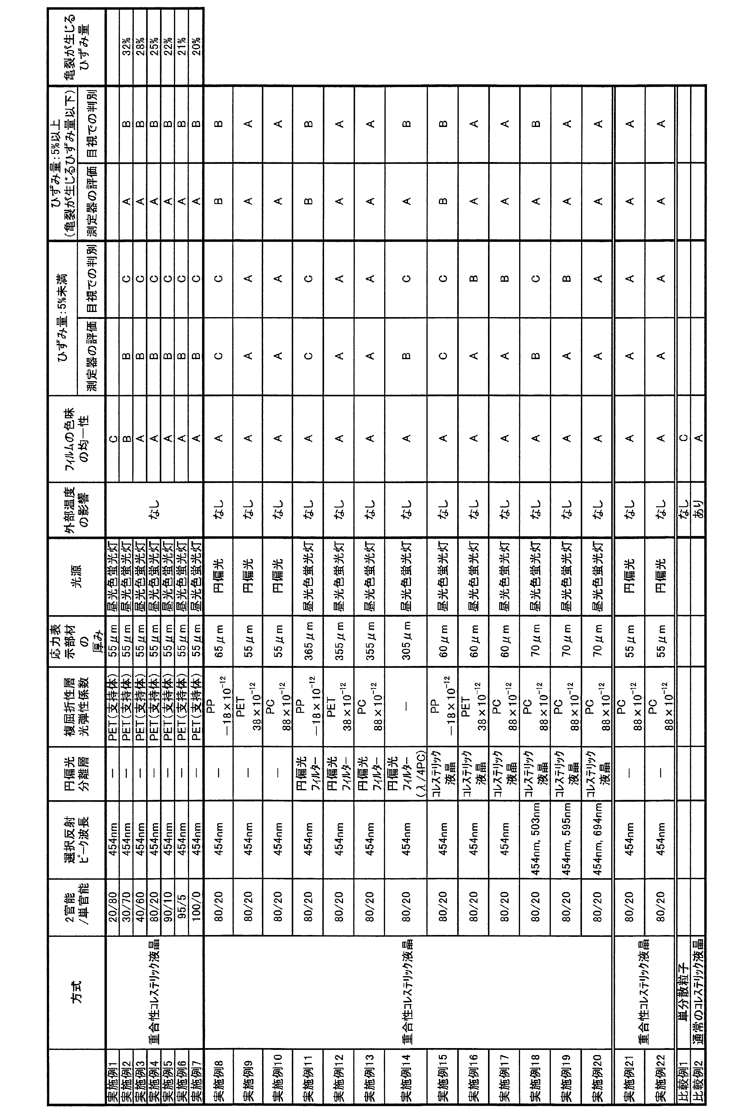
2 複屈折性層
3 支持体
4 円偏光分離層(コレステリック液晶層)
5 直線偏光分離層
6 λ/4位相差層
7 遮光層
8 接着層
Claims (22)
- 選択反射層を含み、
前記選択反射層は重合性液晶化合物を含む液晶組成物の硬化により得られるコレステリック液晶層を1層以上含み、
前記選択反射層は選択反射波長で右円偏光または左円偏光のいずれか一方のセンスの円偏光を選択的に反射する層である応力表示部材。 - 前記重合性液晶化合物が、重合性基を2つ以上有する多官能性液晶化合物と、重合性基を1つのみ有する単官能性液晶化合物とを含み、前記多官能性液晶化合物と前記単官能性液晶化合物との質量比率が30/70~99/1である、請求項1に記載の応力表示部材。
- 複屈折性層をさらに含み、前記複屈折性層は応力が加わると複屈折性が変化する層である、請求項1または2に記載の応力表示部材。
- 複屈折性層の、単位Pa-1で表される光弾性係数の絶対値が20×10-12以上1×10⁻⁶以下である、請求項3に記載の応力表示部材。
- 円偏光分離層をさらに含み、前記円偏光分離層は前記選択反射波長を含む波長域で円偏光を選択的に透過させる層である、請求項3または4に記載の応力表示部材。
- 前記円偏光分離層が透過させる円偏光のセンスが、前記選択反射層が選択的に反射する円偏光のセンスと同一である、請求項5に記載の応力表示部材。
- 前記円偏光分離層が透過させる円偏光のセンスが、前記選択反射層が選択的に反射する円偏光のセンスと逆である、請求項5に記載の応力表示部材。
- 前記選択反射層、前記複屈折性層、前記円偏光分離層をこの順に含む、請求項5~7のいずれか一項に記載の応力表示部材。
- 前記円偏光分離層が、直線偏光分離層とλ/4位相差層とを含む積層体からなる層である請求項5~8のいずれか一項に記載の応力表示部材。
- 前記λ/4位相差層の、単位Pa-1で表される光弾性係数の絶対値が20×10-12以上1×10-6以下である請求項9に記載の応力表示部材。
- 前記円偏光分離層が、重合性液晶化合物を含む液晶組成物の硬化により得られるコレステリック液晶層を含む請求項5~8のいずれか一項に記載の応力表示部材。
- 前記選択反射層に含まれる一層以上のコレステリック液晶層の螺旋ピッチと前記円偏光分離層に含まれる一層以上のコレステリック液晶層の螺旋ピッチとが同一である請求項11に記載の応力表示部材。
- 前記選択反射層が重合性液晶化合物を含む液晶組成物の硬化により得られるコレステリック液晶層を2層以上含み、前記2層以上のコレステリック液晶層の螺旋ピッチが異なっている、請求項3~12のいずれか一項に記載の応力表示部材。
- 前記の2層以上のコレステリック液晶層が円偏光を選択的に反射するピーク波長の差が50nm以上である、請求項13に記載の応力表示部材。
- 1000μm以下の膜厚のフィルムである、請求項1~14のいずれか一項に記載の応力表示部材。
- 接着層を最外層に含む、請求項1~15のいずれか一項に記載の応力表示部材。
- 遮光層を含む、請求項1~16のいずれか一項に記載の応力表示部材。
- 請求項1~17のいずれか一項に記載の応力表示部材を対象物に接着させること、および前記応力表示部材に前記選択反射波長を含む波長域の光を照射して得られる反射光または透過光を測定することを含む、前記対象物のひずみ測定方法。
- 請求項1~16のいずれか一項に記載の応力表示部材、遮光フィルムおよび対象物をこの順となるように配置して前記応力表示部材と前記遮光フィルムと前記対象物とを接着させること、および前記応力表示部材に光を照射して得られる反射光を測定することを含む、前記対象物のひずみ測定方法。
- 請求項3~14のいずれか一項に記載の応力表示部材を対象物に接着させること、および前記選択反射波長を含む波長域の円偏光を前記応力表示部材に照射して得られる反射光を測定することを含む、前記対象物のひずみ測定方法。
- 請求項1~17のいずれか一項に記載の応力表示部材を対象物に接着させること、および前記応力表示部材に光を照射して得られる反射光または透過光を測定することを含み、照射される前記光のピーク波長が前記選択反射層が選択的に光を反射する波長域内にあり、照射される前記光の波長域が前記選択反射層が選択的に光を反射する波長域よりも小さい、前記対象物のひずみ測定方法。
- 視野角制限フィルムを介して前記測定を行う、請求項18~21のいずれか一項に記載のひずみ測定方法。
Priority Applications (4)
| Application Number | Priority Date | Filing Date | Title |
|---|---|---|---|
| KR1020167005259A KR20160035070A (ko) | 2013-08-30 | 2014-08-29 | 응력 표시 부재 및 응력 표시 부재를 이용한 스트레인 측정 방법 |
| CN201480047602.0A CN105492938A (zh) | 2013-08-30 | 2014-08-29 | 应力显示部件及使用应力显示部件的应变测定方法 |
| JP2015534328A JPWO2015030176A1 (ja) | 2013-08-30 | 2014-08-29 | 応力表示部材および応力表示部材を用いたひずみ測定方法 |
| US15/047,861 US20160169664A1 (en) | 2013-08-30 | 2016-02-19 | Stress display member and strain measurement method using stress display member |
Applications Claiming Priority (2)
| Application Number | Priority Date | Filing Date | Title |
|---|---|---|---|
| JP2013179403 | 2013-08-30 | ||
| JP2013-179403 | 2013-08-30 |
Related Child Applications (1)
| Application Number | Title | Priority Date | Filing Date |
|---|---|---|---|
| US15/047,861 Continuation US20160169664A1 (en) | 2013-08-30 | 2016-02-19 | Stress display member and strain measurement method using stress display member |
Publications (1)
| Publication Number | Publication Date |
|---|---|
| WO2015030176A1 true WO2015030176A1 (ja) | 2015-03-05 |
Family
ID=52586723
Family Applications (1)
| Application Number | Title | Priority Date | Filing Date |
|---|---|---|---|
| PCT/JP2014/072743 Ceased WO2015030176A1 (ja) | 2013-08-30 | 2014-08-29 | 応力表示部材および応力表示部材を用いたひずみ測定方法 |
Country Status (5)
| Country | Link |
|---|---|
| US (1) | US20160169664A1 (ja) |
| JP (1) | JPWO2015030176A1 (ja) |
| KR (1) | KR20160035070A (ja) |
| CN (1) | CN105492938A (ja) |
| WO (1) | WO2015030176A1 (ja) |
Cited By (7)
| Publication number | Priority date | Publication date | Assignee | Title |
|---|---|---|---|---|
| CN105547541A (zh) * | 2016-01-05 | 2016-05-04 | 太原理工大学 | 一种单向力监测装置及监测方法 |
| JP2017024376A (ja) * | 2015-07-28 | 2017-02-02 | 大日本印刷株式会社 | 積層体 |
| WO2020022434A1 (ja) * | 2018-07-27 | 2020-01-30 | 富士フイルム株式会社 | 光学素子およびセンサー |
| JPWO2020230700A1 (ja) * | 2019-05-10 | 2020-11-19 | ||
| JPWO2020262474A1 (ja) * | 2019-06-27 | 2020-12-30 | ||
| WO2023026671A1 (ja) * | 2021-08-26 | 2023-03-02 | 富士フイルム株式会社 | 加飾用材料、加飾用材料の製造方法、成型物、加飾用パネル及び電子デバイス |
| US12228645B2 (en) | 2019-05-10 | 2025-02-18 | Fujifilm Corporation | Distance-measuring sensor |
Families Citing this family (11)
| Publication number | Priority date | Publication date | Assignee | Title |
|---|---|---|---|---|
| JP6321418B2 (ja) * | 2014-03-20 | 2018-05-09 | スリーエム イノベイティブ プロパティズ カンパニー | シート及び建造物変形評価用物品 |
| CN106643539B (zh) * | 2016-10-25 | 2019-03-22 | 扬州大学 | 一种基于led彩色发光阵列的结构表面应变直观评价方法 |
| US10247970B2 (en) | 2016-12-20 | 2019-04-02 | Microsoft Technology Licensing, Llc | Measuring strain on display device |
| US10352789B2 (en) | 2017-02-09 | 2019-07-16 | Microsoft Technology Licensing, Llc | Measuring strain on display device |
| CN110476480B (zh) * | 2017-03-30 | 2022-03-15 | 富士胶片株式会社 | 有机el图像显示装置 |
| CN108871219B (zh) * | 2017-05-16 | 2020-12-11 | 北京纳米能源与系统研究所 | 应变传感材料、制备方法及应变传感系统 |
| US10228237B2 (en) * | 2017-07-12 | 2019-03-12 | The Boeing Company | Non-destructive optical method for determining minimum bond strength and proving bond efficacy |
| CN109414200B (zh) * | 2017-12-25 | 2019-12-24 | 深圳市得道健康管理有限公司 | 表面应变检测装置及其表面应变传感器 |
| WO2021020024A1 (ja) * | 2019-07-31 | 2021-02-04 | 日本ゼオン株式会社 | 表示媒体、表示物品及び表示セット |
| CN116953913A (zh) * | 2022-04-18 | 2023-10-27 | 苏州大学 | 一种大口径的薄膜成像器件及其制备方法 |
| CN117554185B (zh) * | 2024-01-11 | 2024-03-15 | 江苏满星测评信息技术有限公司 | 一种薄膜材料力学性能监测方法及系统 |
Citations (2)
| Publication number | Priority date | Publication date | Assignee | Title |
|---|---|---|---|---|
| JPS5531402B2 (ja) * | 1975-04-25 | 1980-08-18 | ||
| JP2009175550A (ja) * | 2008-01-25 | 2009-08-06 | Nippon Zeon Co Ltd | 輝度向上フィルム及び液晶表示装置 |
Family Cites Families (14)
| Publication number | Priority date | Publication date | Assignee | Title |
|---|---|---|---|---|
| US6104448A (en) * | 1991-05-02 | 2000-08-15 | Kent State University | Pressure sensitive liquid crystalline light modulating device and material |
| JPH072050U (ja) * | 1993-06-17 | 1995-01-13 | 株式会社神戸製鋼所 | 色覚型張り合わせフィルム |
| JPH10319235A (ja) * | 1997-05-16 | 1998-12-04 | Nitto Denko Corp | 偏光素子、照明装置及び液晶表示装置 |
| US7218398B2 (en) * | 2003-11-26 | 2007-05-15 | Smith Matthew H | Method and apparatus for determining liquid crystal cell parameters from full Mueller matrix measurements |
| JP4390540B2 (ja) * | 2003-12-02 | 2009-12-24 | 大日本印刷株式会社 | 光学素子及びその製造方法、並びに液晶配向用基板及び液晶表示装置 |
| JP3874200B2 (ja) * | 2004-11-22 | 2007-01-31 | 日東電工株式会社 | 光学補償層付偏光板、液晶パネル、液晶表示装置および光学補償層付偏光板の製造方法 |
| CN100468008C (zh) * | 2006-05-26 | 2009-03-11 | 北京交通大学 | 写有光栅的光子晶体光纤的横向应力传感系统及实现方法 |
| JP5459944B2 (ja) * | 2006-11-13 | 2014-04-02 | 大日本スクリーン製造株式会社 | 表面形状測定装置および応力測定装置、並びに、表面形状測定方法および応力測定方法 |
| JP4905695B2 (ja) * | 2007-03-28 | 2012-03-28 | 学校法人慶應義塾 | 光弾性測定方法およびその装置 |
| JP5493629B2 (ja) * | 2008-11-07 | 2014-05-14 | Jnc株式会社 | 重合性液晶組成物 |
| JP5267066B2 (ja) * | 2008-11-20 | 2013-08-21 | 富士ゼロックス株式会社 | 液晶表示装置 |
| JP5259501B2 (ja) * | 2009-06-11 | 2013-08-07 | 富士フイルム株式会社 | 赤外光反射板、赤外光反射性合わせガラス、並びにコレステリック液晶層を有する積層体及び合わせガラス |
| WO2011092922A1 (ja) * | 2010-01-28 | 2011-08-04 | 日本発條株式会社 | 識別媒体およびその識別方法 |
| JP5457982B2 (ja) * | 2010-08-24 | 2014-04-02 | 富士フイルム株式会社 | 赤外光反射板 |
-
2014
- 2014-08-29 KR KR1020167005259A patent/KR20160035070A/ko not_active Ceased
- 2014-08-29 CN CN201480047602.0A patent/CN105492938A/zh active Pending
- 2014-08-29 WO PCT/JP2014/072743 patent/WO2015030176A1/ja not_active Ceased
- 2014-08-29 JP JP2015534328A patent/JPWO2015030176A1/ja active Pending
-
2016
- 2016-02-19 US US15/047,861 patent/US20160169664A1/en not_active Abandoned
Patent Citations (2)
| Publication number | Priority date | Publication date | Assignee | Title |
|---|---|---|---|---|
| JPS5531402B2 (ja) * | 1975-04-25 | 1980-08-18 | ||
| JP2009175550A (ja) * | 2008-01-25 | 2009-08-06 | Nippon Zeon Co Ltd | 輝度向上フィルム及び液晶表示装置 |
Cited By (13)
| Publication number | Priority date | Publication date | Assignee | Title |
|---|---|---|---|---|
| JP2017024376A (ja) * | 2015-07-28 | 2017-02-02 | 大日本印刷株式会社 | 積層体 |
| CN105547541A (zh) * | 2016-01-05 | 2016-05-04 | 太原理工大学 | 一种单向力监测装置及监测方法 |
| JPWO2020022434A1 (ja) * | 2018-07-27 | 2021-07-01 | 富士フイルム株式会社 | 光学素子およびセンサー |
| WO2020022434A1 (ja) * | 2018-07-27 | 2020-01-30 | 富士フイルム株式会社 | 光学素子およびセンサー |
| US11460729B2 (en) | 2018-07-27 | 2022-10-04 | Fujifilm Corporation | Optical element and sensor |
| JP7015392B2 (ja) | 2018-07-27 | 2022-02-15 | 富士フイルム株式会社 | 光学素子およびセンサー |
| JPWO2020230700A1 (ja) * | 2019-05-10 | 2020-11-19 | ||
| WO2020230700A1 (ja) * | 2019-05-10 | 2020-11-19 | 富士フイルム株式会社 | 光学素子、波長選択フィルタおよびセンサー |
| JP7367010B2 (ja) | 2019-05-10 | 2023-10-23 | 富士フイルム株式会社 | 光学素子、波長選択フィルタおよびセンサー |
| US12228645B2 (en) | 2019-05-10 | 2025-02-18 | Fujifilm Corporation | Distance-measuring sensor |
| JPWO2020262474A1 (ja) * | 2019-06-27 | 2020-12-30 | ||
| JP7317113B2 (ja) | 2019-06-27 | 2023-07-28 | 富士フイルム株式会社 | 成型用加飾フィルム、成型物、及びディスプレイ |
| WO2023026671A1 (ja) * | 2021-08-26 | 2023-03-02 | 富士フイルム株式会社 | 加飾用材料、加飾用材料の製造方法、成型物、加飾用パネル及び電子デバイス |
Also Published As
| Publication number | Publication date |
|---|---|
| KR20160035070A (ko) | 2016-03-30 |
| CN105492938A (zh) | 2016-04-13 |
| JPWO2015030176A1 (ja) | 2017-03-02 |
| US20160169664A1 (en) | 2016-06-16 |
Similar Documents
| Publication | Publication Date | Title |
|---|---|---|
| WO2015030176A1 (ja) | 応力表示部材および応力表示部材を用いたひずみ測定方法 | |
| JP6132678B2 (ja) | 偏光フィルターおよびその応用 | |
| US7393570B2 (en) | Broad-band-cholesteric liquid-crystal film, process for producing the same, circularly polarizing plate, linearly polarizing element, illiminator, and liquid-crystal display | |
| JP6166977B2 (ja) | 円偏光フィルターおよびその応用 | |
| US9874669B2 (en) | Reflection film, optical member, and display | |
| JP6321988B2 (ja) | 遮熱用途に使用可能な反射部材および反射部材を含むプロジェクター | |
| JP6479699B2 (ja) | 車両用画像表示機能付きミラーおよびその製造方法 | |
| JP6254768B2 (ja) | 光を利用した検知システムおよび検知方法 | |
| WO2014181799A1 (ja) | 円偏光分離フィルム、円偏光分離フィルムの製造方法、赤外線センサー、ならびに光を利用した検知システムおよび検知方法 | |
| WO2015025909A1 (ja) | 円偏光フィルターおよびその応用 | |
| JPWO2015159836A1 (ja) | 応力測定方法、応力測定用部材、および応力測定用セット | |
| WO2015050203A1 (ja) | 投映像表示用ハーフミラーおよびその製造方法、ならびに投映像表示システム | |
| WO2015050202A1 (ja) | 投映像表示用ハーフミラーおよび投映像表示システム | |
| JP6286440B2 (ja) | 投映像表示用ハーフミラーおよび投映像表示システム | |
| JP6193471B2 (ja) | 投映像表示用部材および投映像表示用部材を含む投映システム | |
| JP2016004487A (ja) | 光学的パターン読み取り方法、光学的パターン読み取りシステム、光学的パターン読み取り装置、および光学的パターンを含む光学部材 | |
| JP6254770B2 (ja) | 円偏光分離フィルムおよび円偏光分離フィルムの製造方法、ならびに赤外線センサー | |
| JP6254769B2 (ja) | 円偏光分離フィルムおよび円偏光分離フィルムの製造方法、ならびに赤外線センサー | |
| US9910197B2 (en) | Optical member and display including the optical member | |
| WO2016171218A1 (ja) | 検知方法および検知システム | |
| JP2017227924A (ja) | 円偏光分離フィルムおよび円偏光分離フィルムの製造方法、ならびに赤外線センサー | |
| JP2018116308A (ja) | 遮熱用途に使用可能な反射部材および反射部材を含むプロジェクター | |
| JP6588517B2 (ja) | 円偏光分離フィルムおよび円偏光分離フィルムの製造方法、ならびに赤外線センサー | |
| WO2016088709A1 (ja) | 車両用画像表示機能付きミラー |
Legal Events
| Date | Code | Title | Description |
|---|---|---|---|
| WWE | Wipo information: entry into national phase |
Ref document number: 201480047602.0 Country of ref document: CN |
|
| 121 | Ep: the epo has been informed by wipo that ep was designated in this application |
Ref document number: 14840695 Country of ref document: EP Kind code of ref document: A1 |
|
| ENP | Entry into the national phase |
Ref document number: 2015534328 Country of ref document: JP Kind code of ref document: A |
|
| ENP | Entry into the national phase |
Ref document number: 20167005259 Country of ref document: KR Kind code of ref document: A |
|
| NENP | Non-entry into the national phase |
Ref country code: DE |
|
| 122 | Ep: pct application non-entry in european phase |
Ref document number: 14840695 Country of ref document: EP Kind code of ref document: A1 |