WO2015029705A1 - Elément détecteur de faisceau d'énergie à semi-conducteurs - Google Patents
Elément détecteur de faisceau d'énergie à semi-conducteurs Download PDFInfo
- Publication number
- WO2015029705A1 WO2015029705A1 PCT/JP2014/070482 JP2014070482W WO2015029705A1 WO 2015029705 A1 WO2015029705 A1 WO 2015029705A1 JP 2014070482 W JP2014070482 W JP 2014070482W WO 2015029705 A1 WO2015029705 A1 WO 2015029705A1
- Authority
- WO
- WIPO (PCT)
- Prior art keywords
- semiconductor
- semiconductor region
- region
- conductivity type
- main surface
- Prior art date
Links
- 239000004065 semiconductor Substances 0.000 title claims abstract description 457
- 238000001514 detection method Methods 0.000 title claims abstract description 64
- 239000000758 substrate Substances 0.000 claims abstract description 101
- 239000012535 impurity Substances 0.000 claims abstract description 39
- 238000002161 passivation Methods 0.000 claims description 24
- 239000000463 material Substances 0.000 claims description 16
- 229910004298 SiO 2 Inorganic materials 0.000 claims description 6
- 229910018072 Al 2 O 3 Inorganic materials 0.000 claims description 5
- 239000012528 membrane Substances 0.000 claims 1
- 230000004048 modification Effects 0.000 description 21
- 238000012986 modification Methods 0.000 description 21
- 238000000034 method Methods 0.000 description 15
- 238000010586 diagram Methods 0.000 description 11
- 238000009825 accumulation Methods 0.000 description 6
- 230000004888 barrier function Effects 0.000 description 6
- 238000005468 ion implantation Methods 0.000 description 6
- 238000004519 manufacturing process Methods 0.000 description 6
- ZOXJGFHDIHLPTG-UHFFFAOYSA-N Boron Chemical compound [B] ZOXJGFHDIHLPTG-UHFFFAOYSA-N 0.000 description 4
- 229910052796 boron Inorganic materials 0.000 description 4
- 238000009792 diffusion process Methods 0.000 description 3
- 230000008569 process Effects 0.000 description 3
- OAICVXFJPJFONN-UHFFFAOYSA-N Phosphorus Chemical compound [P] OAICVXFJPJFONN-UHFFFAOYSA-N 0.000 description 2
- 229910052787 antimony Inorganic materials 0.000 description 2
- WATWJIUSRGPENY-UHFFFAOYSA-N antimony atom Chemical compound [Sb] WATWJIUSRGPENY-UHFFFAOYSA-N 0.000 description 2
- 229910052785 arsenic Inorganic materials 0.000 description 2
- RQNWIZPPADIBDY-UHFFFAOYSA-N arsenic atom Chemical compound [As] RQNWIZPPADIBDY-UHFFFAOYSA-N 0.000 description 2
- 238000000231 atomic layer deposition Methods 0.000 description 2
- 238000005229 chemical vapour deposition Methods 0.000 description 2
- 229910052698 phosphorus Inorganic materials 0.000 description 2
- 239000011574 phosphorus Substances 0.000 description 2
- 238000000623 plasma-assisted chemical vapour deposition Methods 0.000 description 2
- 230000005855 radiation Effects 0.000 description 2
- 239000011347 resin Substances 0.000 description 2
- 229920005989 resin Polymers 0.000 description 2
- XUIMIQQOPSSXEZ-UHFFFAOYSA-N Silicon Chemical compound [Si] XUIMIQQOPSSXEZ-UHFFFAOYSA-N 0.000 description 1
- 229910020836 Sn-Ag Inorganic materials 0.000 description 1
- 229910020988 Sn—Ag Inorganic materials 0.000 description 1
- XAGFODPZIPBFFR-UHFFFAOYSA-N aluminium Chemical compound [Al] XAGFODPZIPBFFR-UHFFFAOYSA-N 0.000 description 1
- 229910052782 aluminium Inorganic materials 0.000 description 1
- 230000008859 change Effects 0.000 description 1
- 239000012141 concentrate Substances 0.000 description 1
- 239000013078 crystal Substances 0.000 description 1
- 230000007547 defect Effects 0.000 description 1
- 230000005684 electric field Effects 0.000 description 1
- 239000007772 electrode material Substances 0.000 description 1
- 230000003647 oxidation Effects 0.000 description 1
- 238000007254 oxidation reaction Methods 0.000 description 1
- 229910052710 silicon Inorganic materials 0.000 description 1
- 239000010703 silicon Substances 0.000 description 1
- 229910000679 solder Inorganic materials 0.000 description 1
- 238000004544 sputter deposition Methods 0.000 description 1
Images


Classifications
-
- G—PHYSICS
- G01—MEASURING; TESTING
- G01T—MEASUREMENT OF NUCLEAR OR X-RADIATION
- G01T1/00—Measuring X-radiation, gamma radiation, corpuscular radiation, or cosmic radiation
- G01T1/16—Measuring radiation intensity
- G01T1/24—Measuring radiation intensity with semiconductor detectors
-
- H—ELECTRICITY
- H01—ELECTRIC ELEMENTS
- H01L—SEMICONDUCTOR DEVICES NOT COVERED BY CLASS H10
- H01L27/00—Devices consisting of a plurality of semiconductor or other solid-state components formed in or on a common substrate
- H01L27/14—Devices consisting of a plurality of semiconductor or other solid-state components formed in or on a common substrate including semiconductor components sensitive to infrared radiation, light, electromagnetic radiation of shorter wavelength or corpuscular radiation and specially adapted either for the conversion of the energy of such radiation into electrical energy or for the control of electrical energy by such radiation
- H01L27/144—Devices controlled by radiation
- H01L27/1446—Devices controlled by radiation in a repetitive configuration
-
- H—ELECTRICITY
- H01—ELECTRIC ELEMENTS
- H01L—SEMICONDUCTOR DEVICES NOT COVERED BY CLASS H10
- H01L27/00—Devices consisting of a plurality of semiconductor or other solid-state components formed in or on a common substrate
- H01L27/14—Devices consisting of a plurality of semiconductor or other solid-state components formed in or on a common substrate including semiconductor components sensitive to infrared radiation, light, electromagnetic radiation of shorter wavelength or corpuscular radiation and specially adapted either for the conversion of the energy of such radiation into electrical energy or for the control of electrical energy by such radiation
- H01L27/144—Devices controlled by radiation
- H01L27/146—Imager structures
- H01L27/14601—Structural or functional details thereof
- H01L27/14634—Assemblies, i.e. Hybrid structures
Definitions
- the present invention relates to a semiconductor energy ray detecting element for detecting energy rays including high energy radiation such as ⁇ rays or X rays, ultraviolet rays, visible light, infrared rays and the like.
- a semiconductor substrate having a first main surface and a second main surface facing each other, wherein the semiconductor substrate is on a first main surface side of the first conductivity type located on the first main surface side;
- a second semiconductor region of a first conductivity type that is located and has a higher impurity concentration than the first semiconductor region, and is located on the first main surface side and constitutes an energy beam sensitive region with the second semiconductor region;
- a semiconductor energy ray detecting element having a conductive third semiconductor region is known (for example, see Patent Document 1).
- the semiconductor substrate further includes a first conductivity type outer edge semiconductor region which is located along the outer edge of the semiconductor substrate on the first main surface side and has a higher impurity concentration than the first semiconductor region. The outer edge semiconductor region suppresses the depletion layer from reaching the side surface.
- a high bias voltage for example, about several hundred to one thousand volts
- the first semiconductor region needs to be in a fully depleted state in which a depletion layer extending from the third semiconductor region reaches the interface with the second semiconductor region from the first main surface side.
- a high bias voltage is applied to the semiconductor energy ray detection element, the following problems may occur.
- a ROIC (Read-out IC) chip that reads a signal from the semiconductor energy ray detection element is connected to the semiconductor energy ray detection element.
- the semiconductor energy ray detection element and the ROIC chip are arranged close to each other because the corresponding electrodes are bump-connected.
- the outer edge semiconductor region has the same conductivity type as the first semiconductor region, so that the potential of the outer edge semiconductor region is as high as the first semiconductor region. Become. For this reason, the potential difference between the ROIC chip and the outer edge semiconductor region is large, and electric discharge tends to occur between the outer edge semiconductor region and the ROIC chip.
- the electric field tends to concentrate due to the shape (angular shape) of the outer edge of the semiconductor substrate, and electric discharge is likely to occur. If a discharge is generated between the ROIC chip and the semiconductor energy ray detecting element, the element may be destroyed.
- An object of the present invention is to provide a semiconductor energy ray detection element capable of suppressing the occurrence of discharge.
- One aspect of the present invention is a semiconductor energy beam detection element including a semiconductor substrate having a first main surface and a second main surface facing each other, the semiconductor substrate being a first main surface located on the first main surface side.
- the first semiconductor region of the conductivity type and the second semiconductor region located on the second main surface side and having a higher impurity concentration than the first semiconductor region, the first semiconductor region located on the first main surface side, the first The second conductivity type, which is located so as to surround the periphery of the region where the third semiconductor region is located on the first main surface side, and the third semiconductor region of the second conductivity type constituting the energy ray sensitive region with the semiconductor region A fourth semiconductor region, and a fifth semiconductor region of the second conductivity type located along the outer edge of the semiconductor substrate on the first main surface side.
- the semiconductor substrate has a fifth semiconductor region located along the outer edge of the semiconductor substrate on the first main surface side. Since the fifth semiconductor region has a second conductivity type different from the conductivity type of the first semiconductor region, a PN barrier is formed between the first semiconductor region and the fifth semiconductor region.
- a high bias voltage is applied to the semiconductor energy ray detection element, a voltage drop occurs due to the PN barrier formed between the first semiconductor region and the fifth semiconductor region, and the potential of the fifth semiconductor region becomes the first semiconductor region. It falls below the potential of the region. Therefore, the potential difference between the semiconductor substrate (fifth semiconductor region) and the ROIC chip is small, and electric discharge is unlikely to occur between the semiconductor substrate and the ROIC chip.
- discharge is likely to occur at the outer edge of the semiconductor substrate, and a discharge path (current path) is likely to be formed along the side surface of the semiconductor substrate.
- a discharge path current path
- the PN barrier formed between the first semiconductor region and the fifth semiconductor region is located on this current path, it is difficult for current to flow through the current path. This also makes it difficult for discharge to occur between the semiconductor substrate and the ROIC chip.
- the semiconductor substrate is located between the fourth semiconductor region and the fifth semiconductor region so as to surround the fourth semiconductor region on the first main surface side, and has a higher impurity concentration than the first semiconductor region.
- a semiconductor region of the first conductivity type may be further included. In this case, the depletion layer is prevented from reaching the side surface of the semiconductor substrate in a state where the first semiconductor region is completely depleted.
- the semiconductor substrate further includes a first conductivity type semiconductor region located on the side surface so that the first semiconductor region is not exposed on the side surface of the semiconductor substrate and having a higher impurity concentration than the first semiconductor region. May be.
- the depletion layer is prevented from reaching the side surface of the semiconductor substrate in a state where the first semiconductor region is completely depleted.
- the semiconductor energy ray detection element is disposed so as to cover the surface of the first semiconductor region exposed as the side surface of the semiconductor substrate, and a fixed charge having a predetermined polarity exists on the surface side of the covered first semiconductor region.
- a film made of a passivation material may be further provided.
- a fixed charge having a predetermined polarity exists on the surface side of the first semiconductor region covered with the film made of the passivation material.
- the region on the surface side of the first semiconductor region where a fixed charge of a predetermined polarity exists functions as an accumulation layer. Since the film made of the passivation material is positioned on the side surface so that the first semiconductor region is not exposed to the side surface, the depletion layer is reliably suppressed from reaching the side surface of the semiconductor substrate.
- the first conductivity type is P-type
- the second conductivity type is N-type
- passivation material may be Al 2 O 3.
- positive fixed charges exist on the surface side of the first semiconductor region covered with the film made of the passivation material.
- the semiconductor energy ray detection element is disposed so as to cover the surface of the first semiconductor region exposed in the region between the second semiconductor region and the third semiconductor region as the first main surface of the semiconductor substrate.
- a film made of a passivation material for allowing a fixed charge having a predetermined polarity to exist on the surface side of the first semiconductor region may be further provided.
- a fixed charge having a predetermined polarity exists on the surface side of the first semiconductor region covered with the film made of the passivation material.
- the region on the surface side of the first semiconductor region where a fixed charge of a predetermined polarity exists functions as an accumulation layer. Since the film made of the passivation material is disposed so as to cover the surface of the first semiconductor region exposed in the region between the second semiconductor region and the third semiconductor region, the depletion layer reaches the side surface of the semiconductor substrate. To be suppressed.
- the first conductivity type may be N type
- the second conductivity type may be P type
- the passivation material may be SiO 2 or Si 3 N 4 .
- a negative fixed charge exists on the surface side of the first semiconductor region covered with the film made of the passivation material.
- FIG. 1 is a diagram for explaining a cross-sectional configuration of a semiconductor energy ray detection element according to an embodiment.
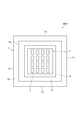
- FIG. 2 is a plan view of the semiconductor energy ray detection element according to the present embodiment.
- FIG. 3 is a diagram for explaining a cross-sectional configuration of the semiconductor energy ray detection element according to the first modification of the present embodiment.
- FIG. 4 is a diagram for explaining a cross-sectional configuration of a semiconductor energy ray detection element according to a second modification of the present embodiment.
- FIG. 5 is a plan view of a semiconductor energy ray detection element according to the second modification.
- FIG. 6 is a diagram for explaining a cross-sectional configuration of a semiconductor energy ray detection element according to a third modification of the present embodiment.
- FIG. 1 is a diagram for explaining a cross-sectional configuration of a semiconductor energy ray detection element according to an embodiment.
- FIG. 2 is a plan view of the semiconductor energy ray detection element according to the present embodiment.
- FIG. 3 is
- FIG. 7 is a diagram for explaining a cross-sectional configuration of a semiconductor energy ray detection element according to a fourth modification of the present embodiment.
- FIG. 8 is a diagram for explaining a cross-sectional configuration of a semiconductor energy beam detection element according to a fifth modification of the present embodiment.
- FIG. 1 is a diagram for explaining a cross-sectional configuration of the semiconductor energy beam detection element according to the present embodiment.
- FIG. 2 is a plan view of the semiconductor energy ray detection element according to the present embodiment. In FIG. 2, illustration of an insulating film 13, electrodes 15, 17, 19, a passivation film 21, and a bump electrode 23 described later is omitted.
- the semiconductor energy ray detection element ED1 includes a semiconductor substrate 1 as shown in FIG.
- the semiconductor substrate 1 is a first conductivity type (for example, P type) silicon substrate having a pair of main surfaces 1a and 1b and a side surface 1c facing each other.
- the side surface 1c extends in the opposing direction of the pair of main surfaces 1a and 1b so as to connect the pair of main surfaces 1a and 1b.
- the semiconductor substrate 1 has a rectangular shape in plan view and has four side surfaces 1c.
- the semiconductor substrate 1 includes a first semiconductor region 3 of a first conductivity type (for example, P type) located on the main surface 1a side and a second of a first conductivity type (for example, P type) located on the main surface 1b side. And a semiconductor region 5.
- the second semiconductor region 5 is a region to which a first conductivity type impurity (such as boron) is added, and has an impurity concentration higher than that of the first semiconductor region 3.
- the second semiconductor region 5 is formed by adding a first conductivity type impurity from the main surface 1b side to the semiconductor substrate 1 by, for example, ion implantation or diffusion.
- the semiconductor substrate 1 has a plurality of second conductivity type (for example, N-type) third semiconductor regions 7 on the main surface 1a side of the semiconductor substrate 1 (first semiconductor region 3). A part of the first semiconductor region 3 is interposed between the third semiconductor regions 7. That is, the third semiconductor regions 7 are separated from each other.
- Each third semiconductor region 7 is a region to which a second conductivity type impurity (such as antimony, arsenic, or phosphorus) is added, and has a higher impurity concentration than the first semiconductor region 3.
- a second conductivity type impurity such as antimony, arsenic, or phosphorus
- a PN junction is formed by the first semiconductor region 3 and each third semiconductor region 7. That is, each third semiconductor region 7 forms an energy ray sensitive region with the first semiconductor region 3.
- the semiconductor substrate 1 has fourth and fifth semiconductor regions 9 and 11 of the second conductivity type (for example, N type) on the main surface 1a side of the semiconductor substrate 1 (first semiconductor region 3).
- the fourth and fifth semiconductor regions 9 and 11 are regions to which a second conductivity type impurity (such as antimony, arsenic, or phosphorus) is added, and the impurity concentration is higher than that of the first semiconductor region 3.
- a second conductivity type impurity such as antimony, arsenic, or phosphorus
- the fourth semiconductor region 9 is positioned so as to surround the periphery of the region where the plurality of third semiconductor regions 7 are located when viewed from the opposing direction of the main surface 1a and the main surface 1b. Yes.
- the fourth semiconductor region 9 functions as a guard ring.
- a partial region of the first semiconductor region 3 is interposed between the third semiconductor region 7 and the fourth semiconductor region 9. That is, the third semiconductor region 7 and the fourth semiconductor region 9 are separated from each other.
- the fifth semiconductor region 11 is located along the outer edge of the semiconductor substrate 1 on the main surface 1a side.
- the fourth semiconductor region 9 is located between the region where the plurality of third semiconductor regions 7 are located and the fifth semiconductor region 11. That is, the fifth semiconductor region 11 is positioned so as to surround the fourth semiconductor region 9 when viewed from the opposing direction of the main surface 1a and the main surface 1b.
- Part of the first semiconductor region 3 is interposed between the fourth semiconductor region 9 and the fifth semiconductor region 11. That is, the fourth semiconductor region 9 and the fifth semiconductor region 11 are separated from each other.
- the third, fourth, and fifth semiconductor regions 7, 9, and 11 are formed by adding a second conductivity type impurity from the main surface 1a side to the semiconductor substrate 1 by, for example, an ion implantation method or a diffusion method.
- an insulating film 13 and electrodes 15, 17, 19 are disposed on the semiconductor substrate 1.
- the insulating film 13 is disposed on the main surface 1 a side of the semiconductor substrate 1 so as to cover the main surface 1 a of the semiconductor substrate 1.
- the insulating film 13 is made of, for example, SiO 2 .
- the insulating film 13 is formed by, for example, a thermal oxidation method, a sputtering method, or a PECVD (Plasma-enhanced Chemical Vapor Deposition) method.
- the electrodes 15, 17, 19 are formed for the corresponding semiconductor regions 7, 9, 11 after removing a part of the insulating film 13 formed on the semiconductor regions 7, 9, 11.
- the electrode 15 is connected to the third semiconductor region 7
- the electrode 17 is connected to the fourth semiconductor region 9
- the electrode 19 is connected to the fifth semiconductor region 11.
- the electrodes 15, 17, 19 are made of an electrode material such as aluminum.
- an electrode connected to the second semiconductor region 5 is also formed on the main surface 1 b side of the semiconductor substrate 1.
- the semiconductor substrate 1 is further provided with a passivation film 21 and a bump electrode 23.
- the passivation film 21 is disposed on the main surface 1 a side of the semiconductor substrate 1 so as to cover the insulating film 13 and the electrodes 15, 17, 19.
- the passivation film 21 is made of SiN, for example.
- the passivation film 21 is formed by, for example, a CVD (Chemical Vapor Deposition) method.
- the bump electrode 23 is formed for each corresponding third semiconductor region 7 after removing a part of the passivation film 21 formed on the third semiconductor region 7.
- the bump electrode 23 is electrically connected to the corresponding electrode 15.
- the bump electrode 23 is made of, for example, Sn—Ag. As a method for forming the bump electrode 23, a method of mounting a solder ball or a printing method can be used.
- the electrodes 17 and 19 are covered with a passivation film 21.
- the semiconductor energy ray detection element ED1 is mounted on the ROIC chip RC as shown in FIG. Specifically, the semiconductor energy ray detection element ED1 is bump-connected to the ROIC chip RC.
- the ROIC chip RC includes a plurality of pad electrodes 25, and the corresponding pad electrodes 25 and bump electrodes 23 are connected.
- the semiconductor energy ray detection element ED1 and the ROIC chip RC are arranged close to each other.
- the main surface 1a of the semiconductor substrate 1 faces the ROIC chip RC.
- a depletion is performed from the third semiconductor region 7 to the first semiconductor region 3 by applying a bias voltage (reverse bias voltage) between the second semiconductor region 5 and the third semiconductor region 7.
- the layer expands.
- a state where the depletion layer reaches the second semiconductor region 5 is a completely depleted state.
- the semiconductor substrate 1 has the fifth semiconductor region 11 positioned along the outer edge of the semiconductor substrate 1 on the main surface 1a side. Since the fifth semiconductor region 11 has a second conductivity type different from the conductivity type of the first semiconductor region 3, a PN barrier is formed between the first semiconductor region 3 and the fifth semiconductor region.
- a high bias voltage for example, about several hundred to one thousand volts
- the voltage is caused by the PN barrier formed between the first semiconductor region 3 and the fifth semiconductor region 11.
- a drop occurs, and the potential of the fifth semiconductor region 11 falls below the potential of the first semiconductor region 3. Therefore, the potential difference between the semiconductor substrate 1 (fifth semiconductor region 11) and the ROIC chip RC is small, and electric discharge is unlikely to occur between the semiconductor substrate 1 and the ROIC chip RC.
- the semiconductor energy beam detection element ED1 can suppress the occurrence of discharge. It is possible to suppress the depletion layer from reaching the side surface 1c by setting the distance between the fourth semiconductor region 9 and the fifth semiconductor region 11 to a predetermined value.
- a configuration for suppressing discharge between the semiconductor substrate and the ROIC chip a configuration in which the potential difference between the semiconductor substrate and the ROIC chip is reduced is conceivable.
- a double-sided structure in which the potential on the pair of main surfaces is approximately the same as the potential of the ROIC chip at the end of the semiconductor substrate may be adopted for the semiconductor energy ray detection element.
- the above-described manufacturing process can be prevented from becoming complicated and expensive.
- a configuration in which an insulating resin is filled between the end portion of the semiconductor substrate and the ROIC chip can be considered as a countermeasure against discharge.
- the step of filling the insulating resin needs to be added when the semiconductor energy ray detection is mounted on the ROIC chip or after the mounting, the manufacturing process becomes complicated as a result. Inevitable.
- the semiconductor energy ray detection element ED1 of the present embodiment since the semiconductor substrate 1 has the fifth semiconductor region 11, the occurrence of discharge is suppressed, so that the manufacturing process is complicated and the cost is high. There is no inconvenience.
- FIG. 3 is a diagram for explaining a cross-sectional configuration of the semiconductor energy ray detection element according to the first modification of the present embodiment.
- the semiconductor substrate 1 has a first conductivity type (for example, P-type) semiconductor region 31 on the main surface 1a side of the semiconductor substrate 1 (first semiconductor region 3).
- the semiconductor region 31 is located between the fourth semiconductor region 9 and the fifth semiconductor region 11 so as to surround the fourth semiconductor region 9 when viewed from the opposing direction of the main surface 1a and the main surface 1b.
- the semiconductor region 31 is a region to which an impurity of the first conductivity type (boron or the like) is added, and has an impurity concentration higher than that of the first semiconductor region 3.
- the semiconductor region 31 is in contact with the fourth semiconductor region 9 and the fifth semiconductor region 11. For this reason, the impurity concentration in the semiconductor region 31 is preferably lower than the impurity concentration in the third, fourth, and fifth semiconductor regions 7, 9, 11.
- the thickness of the semiconductor region 31 is smaller than the thickness of the third, fourth, and fifth semiconductor regions 7, 9, 11.
- the semiconductor region 31 is formed by, for example, an ion implantation method.
- the semiconductor region 31 is formed by an ion implantation method without using a mask in which a predetermined opening is formed, the first semiconductor region 3 exposed as the main surface 1a of the semiconductor substrate 1 is exposed on the surface side of the first semiconductor region 3.
- a conductive type (for example, P type) semiconductor region 33 is also formed.
- the semiconductor regions 33 are formed between the third semiconductor regions 7 and between the third semiconductor region 7 and the fourth semiconductor region 9, respectively.
- a region where impurities of the first conductivity type (for example, P-type) exist also on the surface side of the third, fourth, and fifth semiconductor regions 7, 9, 11 exposed as the main surface 1a of the semiconductor substrate 1 35 is formed.
- the impurity concentrations in the semiconductor regions 31 and 33 are set lower than the impurity concentrations in the third, fourth, and fifth semiconductor regions 7, 9, and 11, so that the third, fourth, and fifth. It is possible to suppress the occurrence of trouble in the functions of the semiconductor regions 7, 9, and 11.
- the semiconductor substrate 1 is located between the fourth semiconductor region 9 and the fifth semiconductor region 11 so as to surround the periphery of the fourth semiconductor region 9 on the main surface 1 a side, and from the first semiconductor region 3.
- the semiconductor region 31 of the first conductivity type having a high impurity concentration This suppresses the depletion layer from reaching the side surface 1c of the semiconductor substrate 1 in a state where the first semiconductor region 3 is completely depleted.
- FIG. 4 is a diagram for explaining a cross-sectional configuration of a semiconductor energy ray detection element according to a second modification of the present embodiment.
- FIG. 5 is a plan view of a semiconductor energy ray detection element according to the second modification.
- illustration of the insulating film 13, the electrodes 15, 17, 19, the passivation film 21, and the bump electrode 23 is omitted.
- the semiconductor substrate 1 has a first conductivity type (for example, P-type) semiconductor region 37 on the main surface 1a side of the semiconductor substrate 1 (first semiconductor region 3).
- the semiconductor region 37 is located between the fourth semiconductor region 9 and the fifth semiconductor region 11 so as to surround the fourth semiconductor region 9 when viewed from the opposing direction of the main surface 1a and the main surface 1b.
- the semiconductor region 37 is a region to which a first conductivity type impurity (such as boron) is added, and has an impurity concentration higher than that of the first semiconductor region 3.
- the semiconductor region 37 is formed by adding a first conductivity type impurity from the main surface 1a side to the semiconductor substrate 1 by, for example, an ion implantation method or a diffusion method.
- a part of the first semiconductor region 3 is interposed between the fourth semiconductor region 9 and the semiconductor region 37, and the first semiconductor region 3 is also interposed between the fifth semiconductor region 11 and the semiconductor region 37. Is partly intervened. That is, the fourth semiconductor region 9 and the semiconductor region 37 are separated from each other, and the fifth semiconductor region 11 and the semiconductor region 37 are separated from each other. Therefore, the impurity concentration of the semiconductor region 37 can be set higher than the impurity concentration of the semiconductor region 31 described above.
- the impurity concentration in the semiconductor region 37 may be approximately the same as the impurity concentration in the third, fourth, and fifth semiconductor regions 7, 9, and 11.
- the thickness of the semiconductor region 37 is smaller than the thicknesses of the third, fourth, and fifth semiconductor regions 7, 9, 11.
- the semiconductor substrate 1 is located between the fourth semiconductor region 9 and the fifth semiconductor region 11 so as to surround the periphery of the fourth semiconductor region 9 on the main surface 1 a side, and from the first semiconductor region 3. Also has a first conductivity type semiconductor region 37 having a high impurity concentration. This suppresses the depletion layer from reaching the side surface 1c of the semiconductor substrate 1 in a state where the first semiconductor region 3 is completely depleted.
- FIG. 6 is a diagram for explaining a cross-sectional configuration of a semiconductor energy ray detection element according to a third modification of the present embodiment.
- the semiconductor substrate 1 has a semiconductor region 39 located on the side surface 1c side so that the first semiconductor region 3 is not exposed to the side surface 1c.
- the semiconductor region 39 extends in the opposing direction of the pair of main surfaces 1a and 1b so that the first semiconductor region 3 is not exposed to the side surface 1c.
- the edge on the main surface 1 a side in the semiconductor region 39 is in contact with the fifth semiconductor region 11.
- the edge on the main surface 1 b side in the semiconductor region 39 is in contact with the second semiconductor region 5.
- the semiconductor region 39 is a region to which a first conductivity type impurity (such as boron) is added, and has an impurity concentration higher than that of the first semiconductor region 3. Since the semiconductor region 39 is in contact with the fifth semiconductor region 11, the impurity concentration in the semiconductor region 39 is preferably lower than the impurity concentration in the fifth semiconductor region 11.
- the semiconductor region 39 is formed by, for example, an ion implantation method.
- the semiconductor substrate 1 is located on the side surface 1c side so that the first semiconductor region 3 is not exposed to the side surface 1c, and the first conductivity type semiconductor region 39 having a higher impurity concentration than the first semiconductor region 3 is formed. Have. This suppresses the depletion layer from reaching the side surface 1c of the semiconductor substrate 1 in a state where the first semiconductor region 3 is completely depleted.
- the semiconductor substrate 1 does not necessarily have the semiconductor region 37.
- the semiconductor substrate 1 since the impurity concentration of the semiconductor region 39 is set to be relatively low, in order to reliably suppress the depletion layer from reaching the side surface 1c of the semiconductor substrate 1, the semiconductor substrate 1 is made of a semiconductor. It is preferable to have the region 37.
- FIG. 7 is a diagram for explaining a cross-sectional configuration of a semiconductor energy ray detection element according to a fourth modification of the present embodiment.
- the semiconductor energy ray detection element ED5 includes a film 41 made of Al 2 O 3 .
- the film 41 is disposed so as to cover the surface of the first semiconductor region 3 exposed as the side surface 1 c of the semiconductor substrate 1.
- Al 2 O 3 is a passivation material for allowing positive fixed charges to exist on the surface side of the covered first semiconductor region 3.
- the film 41 is formed on the side surface 1 c of the semiconductor substrate 1, and the side surface 1 c is covered with the film 41. That is, not only the first semiconductor region 3 but also the surfaces of the second semiconductor region 5 and the fifth semiconductor region 11 exposed as the side surface 1 c of the semiconductor substrate 1 are covered with the film 41.
- the film 41 is formed by, for example, an ALD (Atomic Layer Deposition) method.
- a fixed charge (positive fixed charge) having a predetermined polarity exists on the surface side of the first semiconductor region 3 covered with the film 41 made of Al 2 O 3 .
- the region on the surface side of the first semiconductor region 3 where positive fixed charges are present functions as an accumulation layer 43.
- the film 41 extends in the thickness direction of the semiconductor substrate 1 across the interface with the fifth semiconductor region 11 and the interface with the second semiconductor region 5 on the surface of the first semiconductor region 3. This suppresses the depletion layer from reaching the side surface 1c of the semiconductor substrate 1 in a state where the first semiconductor region 3 is completely depleted.
- the film 41 covers not only the surface of the first semiconductor region 3 but also the surfaces of the second semiconductor region 5 and the fifth semiconductor region 11 on the side surface 1 c of the semiconductor substrate 1. Thereby, since the surface of the first semiconductor region 3 is reliably covered with the film 41, the depletion layer can more reliably reach the surface of the first semiconductor region 3 (side surface 1c of the semiconductor substrate 1). Can be suppressed.
- the semiconductor substrate 1 does not necessarily have the semiconductor region 37.
- the semiconductor substrate 1 in order to reliably suppress the depletion layer from reaching the side surface 1 c of the semiconductor substrate 1, the semiconductor substrate 1 preferably has the semiconductor region 37.
- the first conductivity type may be an N type and the second conductivity type may be a P type.
- the insulating film 13 is preferably made of the above-described SiO 2 or Si 3 N 4 .
- SiO 2 or Si 3 N 4 is a passivation material for causing negative fixed charges to exist on the surface side of the covered N-type first semiconductor region 3.
- the insulating film 13 is disposed so as to cover the surface of the first semiconductor region 3 exposed as the main surface 1 a of the semiconductor substrate 1. Therefore, the insulating film 13, when formed of SiO 2 or Si 3 N 4, on the surface side of the first semiconductor region 3 which is covered with the insulating film 13, a predetermined polarity fixed charge (negative charge) is present To do.
- the region on the surface side of the first semiconductor region 3 where the negative fixed charge exists functions as an accumulation layer 45 as shown in FIG.
- a region located between the fourth semiconductor region 9 and the fifth semiconductor region 11 electrically isolates the fourth semiconductor region 9 and the fifth semiconductor region 11. This suppresses the depletion layer from reaching the side surface 1c of the semiconductor substrate 1 in a state where the first semiconductor region 3 is completely depleted.
- the shape of the semiconductor substrate 1, the number and shape of the third semiconductor regions 7, and the shapes of the fourth and fifth semiconductor regions 9 and 11 are not limited to the above-described embodiments and modifications.
- the present invention can be used for a semiconductor energy ray detection element that detects energy rays including high energy radiation such as ⁇ rays or X rays, ultraviolet rays, visible light, or infrared rays.
- SYMBOLS 1 Semiconductor substrate, 1a, 1b ... Main surface, 1c ... Side surface, 3 ... First semiconductor region, 5 ... Second semiconductor region, 7 ... Third semiconductor region, 9 ... Fourth semiconductor region, 11 ... Fifth semiconductor region , 13 ... Insulating film, 31, 37, 39 ... Semiconductor region, 41 ... Film, 43, 45 ... Accumulation layer, ED1, ED2, ED3, ED4, ED5 ... Semiconductor energy beam detecting element.
Landscapes
- Physics & Mathematics (AREA)
- Engineering & Computer Science (AREA)
- Power Engineering (AREA)
- General Physics & Mathematics (AREA)
- Computer Hardware Design (AREA)
- Condensed Matter Physics & Semiconductors (AREA)
- Electromagnetism (AREA)
- Microelectronics & Electronic Packaging (AREA)
- Health & Medical Sciences (AREA)
- Life Sciences & Earth Sciences (AREA)
- High Energy & Nuclear Physics (AREA)
- Molecular Biology (AREA)
- Spectroscopy & Molecular Physics (AREA)
- Light Receiving Elements (AREA)
- Measurement Of Radiation (AREA)
Abstract
La présente invention concerne un élément (ED1) détecteur de faisceau d'énergie à semi-conducteur qui est doté d'un substrat (1) à semi-conducteur ayant une surface (1a) principale et une surface (1b) principale se faisant face. Le substrat (1) à semi-conducteur possède : une première zone (3) à semi-conducteur d'un premier type de conductivité, la première zone (3) à semi-conducteur étant disposée côté surface (1a) principale ; une deuxième zone (5) à semi-conducteur du premier type de conductivité ayant une concentration plus élevée en impuretés que celle de la première zone (3) à semi-conducteur, la deuxième zone (5) à semi-conducteur étant positionnée côté surface (1b) principale ; une troisième zone (7) à semi-conducteur d'un second type de conductivité et constituant une zone sensible au faisceau d'énergie dotée de la première zone (3) à semi-conducteur, la troisième zone (7) à semi-conducteur étant positionnée côté surface (1a) principale ; une quatrième zone (9) à semi-conducteur du second type de conductivité, la quatrième zone (9) à semi-conducteur étant positionnée côté surface (1a) principale pour entourer la zone dans laquelle la troisième zone (7) à semi-conducteur est positionnée ; et une cinquième zone (11) à semi-conducteur du second type de conductivité, la cinquième zone (11) à semi-conducteur étant positionnée côté surface (1a) principale pour suivre le bord extérieur du substrat (1) à semi-conducteur.
Applications Claiming Priority (2)
| Application Number | Priority Date | Filing Date | Title |
|---|---|---|---|
| JP2013-179147 | 2013-08-30 | ||
| JP2013179147A JP6170379B2 (ja) | 2013-08-30 | 2013-08-30 | 半導体エネルギー線検出素子 |
Publications (1)
| Publication Number | Publication Date |
|---|---|
| WO2015029705A1 true WO2015029705A1 (fr) | 2015-03-05 |
Family
ID=52586277
Family Applications (1)
| Application Number | Title | Priority Date | Filing Date |
|---|---|---|---|
| PCT/JP2014/070482 WO2015029705A1 (fr) | 2013-08-30 | 2014-08-04 | Elément détecteur de faisceau d'énergie à semi-conducteurs |
Country Status (2)
| Country | Link |
|---|---|
| JP (1) | JP6170379B2 (fr) |
| WO (1) | WO2015029705A1 (fr) |
Cited By (1)
| Publication number | Priority date | Publication date | Assignee | Title |
|---|---|---|---|---|
| CN111066156A (zh) * | 2017-09-08 | 2020-04-24 | 浜松光子学株式会社 | 半导体晶片的制造方法、半导体能量线检测元件的制造方法及半导体晶片 |
Families Citing this family (2)
| Publication number | Priority date | Publication date | Assignee | Title |
|---|---|---|---|---|
| WO2017150616A1 (fr) * | 2016-03-03 | 2017-09-08 | 浜松ホトニクス株式会社 | Élément semi-conducteur de détection de lumière |
| US11215698B2 (en) | 2016-08-29 | 2022-01-04 | Hamamatsu Photonics K.K. | Distance sensor and distance image sensor |
Citations (7)
| Publication number | Priority date | Publication date | Assignee | Title |
|---|---|---|---|---|
| JPH01216581A (ja) * | 1988-02-25 | 1989-08-30 | Fuji Electric Co Ltd | 半導体装置 |
| JPH05275731A (ja) * | 1992-03-25 | 1993-10-22 | Sharp Corp | フォトダイオード |
| JP2002314120A (ja) * | 2001-04-18 | 2002-10-25 | Hamamatsu Photonics Kk | ホトダイオード |
| JP2007335596A (ja) * | 2006-06-14 | 2007-12-27 | Hamamatsu Photonics Kk | フォトダイオードアレイ |
| JP2010239005A (ja) * | 2009-03-31 | 2010-10-21 | Kinki Univ | 裏面照射型撮像素子の製造方法、その製造方法により製造された裏面照射型撮像素子及びそれを備えた撮像装置 |
| JP2011138905A (ja) * | 2009-12-28 | 2011-07-14 | Toshiba Corp | 固体撮像装置 |
| WO2012117931A1 (fr) * | 2011-03-02 | 2012-09-07 | ソニー株式会社 | Dispositif d'imagerie à semi-conducteurs et son procédé de fabrication, et instrument électronique |
Family Cites Families (1)
| Publication number | Priority date | Publication date | Assignee | Title |
|---|---|---|---|---|
| GB0921053D0 (en) * | 2009-12-01 | 2010-01-13 | Selex Sensors & Airborne Sys | Infra red detectors and methods of manufacture |
-
2013
- 2013-08-30 JP JP2013179147A patent/JP6170379B2/ja not_active Expired - Fee Related
-
2014
- 2014-08-04 WO PCT/JP2014/070482 patent/WO2015029705A1/fr active Application Filing
Patent Citations (7)
| Publication number | Priority date | Publication date | Assignee | Title |
|---|---|---|---|---|
| JPH01216581A (ja) * | 1988-02-25 | 1989-08-30 | Fuji Electric Co Ltd | 半導体装置 |
| JPH05275731A (ja) * | 1992-03-25 | 1993-10-22 | Sharp Corp | フォトダイオード |
| JP2002314120A (ja) * | 2001-04-18 | 2002-10-25 | Hamamatsu Photonics Kk | ホトダイオード |
| JP2007335596A (ja) * | 2006-06-14 | 2007-12-27 | Hamamatsu Photonics Kk | フォトダイオードアレイ |
| JP2010239005A (ja) * | 2009-03-31 | 2010-10-21 | Kinki Univ | 裏面照射型撮像素子の製造方法、その製造方法により製造された裏面照射型撮像素子及びそれを備えた撮像装置 |
| JP2011138905A (ja) * | 2009-12-28 | 2011-07-14 | Toshiba Corp | 固体撮像装置 |
| WO2012117931A1 (fr) * | 2011-03-02 | 2012-09-07 | ソニー株式会社 | Dispositif d'imagerie à semi-conducteurs et son procédé de fabrication, et instrument électronique |
Cited By (2)
| Publication number | Priority date | Publication date | Assignee | Title |
|---|---|---|---|---|
| CN111066156A (zh) * | 2017-09-08 | 2020-04-24 | 浜松光子学株式会社 | 半导体晶片的制造方法、半导体能量线检测元件的制造方法及半导体晶片 |
| CN111066156B (zh) * | 2017-09-08 | 2023-08-29 | 浜松光子学株式会社 | 半导体晶片的制造方法、半导体能量线检测元件的制造方法及半导体晶片 |
Also Published As
| Publication number | Publication date |
|---|---|
| JP6170379B2 (ja) | 2017-07-26 |
| JP2015050223A (ja) | 2015-03-16 |
Similar Documents
| Publication | Publication Date | Title |
|---|---|---|
| TWI614882B (zh) | 光檢測裝置 | |
| JP2012182381A (ja) | 半導体装置 | |
| TW201434142A (zh) | 光二極體陣列 | |
| TWI704686B (zh) | 光檢測裝置 | |
| US8981439B2 (en) | Solid-state imaging device and image capturing system | |
| EP2808705B1 (fr) | Détecteur à semi-conducteur avec protection contre le rayonnement | |
| US20150008544A1 (en) | Physical quantity sensor | |
| US9780140B2 (en) | X-ray image sensor substrate | |
| KR100850289B1 (ko) | 적층 구조의 이미지센서 및 그 제조방법 | |
| WO2015029705A1 (fr) | Elément détecteur de faisceau d'énergie à semi-conducteurs | |
| KR20180119628A (ko) | 반도체 광검출 소자 | |
| JP2008172217A (ja) | 固体撮像装置 | |
| TW201804629A (zh) | 放射線檢測器及其製造方法 | |
| US10461115B2 (en) | Photodiode array | |
| TWI591808B (zh) | Photo diode array | |
| JP4816603B2 (ja) | 固体撮像素子の製造方法 | |
| TWI806960B (zh) | 光檢測裝置 | |
| JP4858367B2 (ja) | 固体撮像素子の製造方法 | |
| EP2573814B1 (fr) | Capteur d'image à semi-conducteur | |
| JP2013145180A (ja) | 放射線検出器,放射線検出装置及びそれらの動作方法 | |
| JP2020085498A (ja) | 湿度検出装置及び温度検出装置 | |
| US11398572B2 (en) | Semiconductor wafer manufacturing method, method of manufacturing semiconductor energy beam detecting element, and semiconductor wafer | |
| JP2017157736A (ja) | 受光素子を有する半導体装置 | |
| JP2001274450A (ja) | β線検出器 | |
| JP4816602B2 (ja) | 固体撮像素子の製造方法 |
Legal Events
| Date | Code | Title | Description |
|---|---|---|---|
| 121 | Ep: the epo has been informed by wipo that ep was designated in this application |
Ref document number: 14840862 Country of ref document: EP Kind code of ref document: A1 |
|
| NENP | Non-entry into the national phase |
Ref country code: DE |
|
| 122 | Ep: pct application non-entry in european phase |
Ref document number: 14840862 Country of ref document: EP Kind code of ref document: A1 |